JP5399608B2 - Method for manufacturing thin film transistor substrate - Google Patents
Method for manufacturing thin film transistor substrate Download PDFInfo
- Publication number
- JP5399608B2 JP5399608B2 JP2006209726A JP2006209726A JP5399608B2 JP 5399608 B2 JP5399608 B2 JP 5399608B2 JP 2006209726 A JP2006209726 A JP 2006209726A JP 2006209726 A JP2006209726 A JP 2006209726A JP 5399608 B2 JP5399608 B2 JP 5399608B2
- Authority
- JP
- Japan
- Prior art keywords
- semiconductor layer
- region
- ion implantation
- lightly doped
- thin film
- Prior art date
- Legal status (The legal status is an assumption and is not a legal conclusion. Google has not performed a legal analysis and makes no representation as to the accuracy of the status listed.)
- Expired - Fee Related
Links
- 239000000758 substrate Substances 0.000 title claims description 91
- 239000010409 thin film Substances 0.000 title claims description 87
- 238000000034 method Methods 0.000 title claims description 27
- 238000004519 manufacturing process Methods 0.000 title claims description 19
- 239000010408 film Substances 0.000 claims description 178
- 239000004065 semiconductor Substances 0.000 claims description 112
- 239000012535 impurity Substances 0.000 claims description 46
- 150000002500 ions Chemical class 0.000 claims description 41
- 238000005468 ion implantation Methods 0.000 claims description 30
- 229910021420 polycrystalline silicon Inorganic materials 0.000 claims description 21
- 238000005530 etching Methods 0.000 claims description 12
- 229920002120 photoresistant polymer Polymers 0.000 claims description 12
- 230000000903 blocking effect Effects 0.000 claims description 11
- 238000000059 patterning Methods 0.000 claims description 11
- 238000004380 ashing Methods 0.000 claims description 5
- 239000007943 implant Substances 0.000 claims description 5
- 239000010410 layer Substances 0.000 description 126
- 239000011229 interlayer Substances 0.000 description 23
- 229910052581 Si3N4 Inorganic materials 0.000 description 6
- VYPSYNLAJGMNEJ-UHFFFAOYSA-N Silicium dioxide Chemical compound O=[Si]=O VYPSYNLAJGMNEJ-UHFFFAOYSA-N 0.000 description 6
- 229910021417 amorphous silicon Inorganic materials 0.000 description 6
- 239000003990 capacitor Substances 0.000 description 6
- HQVNEWCFYHHQES-UHFFFAOYSA-N silicon nitride Chemical compound N12[Si]34N5[Si]62N3[Si]51N64 HQVNEWCFYHHQES-UHFFFAOYSA-N 0.000 description 6
- 239000002356 single layer Substances 0.000 description 6
- 238000002425 crystallisation Methods 0.000 description 5
- 230000008025 crystallization Effects 0.000 description 5
- 229910052814 silicon oxide Inorganic materials 0.000 description 5
- 238000002513 implantation Methods 0.000 description 4
- 239000004973 liquid crystal related substance Substances 0.000 description 4
- 238000000206 photolithography Methods 0.000 description 4
- XLOMVQKBTHCTTD-UHFFFAOYSA-N Zinc monoxide Chemical compound [Zn]=O XLOMVQKBTHCTTD-UHFFFAOYSA-N 0.000 description 3
- 229910044991 metal oxide Inorganic materials 0.000 description 3
- 150000004706 metal oxides Chemical class 0.000 description 3
- 238000003860 storage Methods 0.000 description 3
- QVGXLLKOCUKJST-UHFFFAOYSA-N atomic oxygen Chemical compound [O] QVGXLLKOCUKJST-UHFFFAOYSA-N 0.000 description 2
- 238000000151 deposition Methods 0.000 description 2
- 238000010586 diagram Methods 0.000 description 2
- 238000010438 heat treatment Methods 0.000 description 2
- AMGQUBHHOARCQH-UHFFFAOYSA-N indium;oxotin Chemical compound [In].[Sn]=O AMGQUBHHOARCQH-UHFFFAOYSA-N 0.000 description 2
- 239000011810 insulating material Substances 0.000 description 2
- 238000010030 laminating Methods 0.000 description 2
- 239000011159 matrix material Substances 0.000 description 2
- 229910052751 metal Inorganic materials 0.000 description 2
- 239000002184 metal Substances 0.000 description 2
- 229910052760 oxygen Inorganic materials 0.000 description 2
- 239000001301 oxygen Substances 0.000 description 2
- 238000001259 photo etching Methods 0.000 description 2
- 238000000623 plasma-assisted chemical vapour deposition Methods 0.000 description 2
- VYZAMTAEIAYCRO-UHFFFAOYSA-N Chromium Chemical compound [Cr] VYZAMTAEIAYCRO-UHFFFAOYSA-N 0.000 description 1
- ZOKXTWBITQBERF-UHFFFAOYSA-N Molybdenum Chemical compound [Mo] ZOKXTWBITQBERF-UHFFFAOYSA-N 0.000 description 1
- 206010034972 Photosensitivity reaction Diseases 0.000 description 1
- WZMARNWNQFFBKK-UHFFFAOYSA-N [In+3].[O-2].[Zn+2].[In+3].[O-2].[O-2].[O-2] Chemical compound [In+3].[O-2].[Zn+2].[In+3].[O-2].[O-2].[O-2] WZMARNWNQFFBKK-UHFFFAOYSA-N 0.000 description 1
- 230000003213 activating effect Effects 0.000 description 1
- 229910045601 alloy Inorganic materials 0.000 description 1
- 239000000956 alloy Substances 0.000 description 1
- 229910052782 aluminium Inorganic materials 0.000 description 1
- XAGFODPZIPBFFR-UHFFFAOYSA-N aluminium Chemical compound [Al] XAGFODPZIPBFFR-UHFFFAOYSA-N 0.000 description 1
- 230000015572 biosynthetic process Effects 0.000 description 1
- 229910052804 chromium Inorganic materials 0.000 description 1
- 239000011651 chromium Substances 0.000 description 1
- 230000000295 complement effect Effects 0.000 description 1
- 239000004020 conductor Substances 0.000 description 1
- 230000005684 electric field Effects 0.000 description 1
- 239000011521 glass Substances 0.000 description 1
- 238000009413 insulation Methods 0.000 description 1
- 238000005224 laser annealing Methods 0.000 description 1
- 229910052750 molybdenum Inorganic materials 0.000 description 1
- 239000011733 molybdenum Substances 0.000 description 1
- 239000011368 organic material Substances 0.000 description 1
- 230000036211 photosensitivity Effects 0.000 description 1
- 239000010453 quartz Substances 0.000 description 1
- 229910052594 sapphire Inorganic materials 0.000 description 1
- 239000010980 sapphire Substances 0.000 description 1
- 238000007711 solidification Methods 0.000 description 1
- 230000008023 solidification Effects 0.000 description 1
- YVTHLONGBIQYBO-UHFFFAOYSA-N zinc indium(3+) oxygen(2-) Chemical compound [O--].[Zn++].[In+3] YVTHLONGBIQYBO-UHFFFAOYSA-N 0.000 description 1
- 239000011787 zinc oxide Substances 0.000 description 1
Images


Classifications
-
- G—PHYSICS
- G02—OPTICS
- G02F—OPTICAL DEVICES OR ARRANGEMENTS FOR THE CONTROL OF LIGHT BY MODIFICATION OF THE OPTICAL PROPERTIES OF THE MEDIA OF THE ELEMENTS INVOLVED THEREIN; NON-LINEAR OPTICS; FREQUENCY-CHANGING OF LIGHT; OPTICAL LOGIC ELEMENTS; OPTICAL ANALOGUE/DIGITAL CONVERTERS
- G02F1/00—Devices or arrangements for the control of the intensity, colour, phase, polarisation or direction of light arriving from an independent light source, e.g. switching, gating or modulating; Non-linear optics
- G02F1/01—Devices or arrangements for the control of the intensity, colour, phase, polarisation or direction of light arriving from an independent light source, e.g. switching, gating or modulating; Non-linear optics for the control of the intensity, phase, polarisation or colour
- G02F1/13—Devices or arrangements for the control of the intensity, colour, phase, polarisation or direction of light arriving from an independent light source, e.g. switching, gating or modulating; Non-linear optics for the control of the intensity, phase, polarisation or colour based on liquid crystals, e.g. single liquid crystal display cells
- G02F1/133—Constructional arrangements; Operation of liquid crystal cells; Circuit arrangements
- G02F1/136—Liquid crystal cells structurally associated with a semi-conducting layer or substrate, e.g. cells forming part of an integrated circuit
-
- H—ELECTRICITY
- H01—ELECTRIC ELEMENTS
- H01L—SEMICONDUCTOR DEVICES NOT COVERED BY CLASS H10
- H01L27/00—Devices consisting of a plurality of semiconductor or other solid-state components formed in or on a common substrate
- H01L27/02—Devices consisting of a plurality of semiconductor or other solid-state components formed in or on a common substrate including semiconductor components specially adapted for rectifying, oscillating, amplifying or switching and having at least one potential-jump barrier or surface barrier; including integrated passive circuit elements with at least one potential-jump barrier or surface barrier
- H01L27/12—Devices consisting of a plurality of semiconductor or other solid-state components formed in or on a common substrate including semiconductor components specially adapted for rectifying, oscillating, amplifying or switching and having at least one potential-jump barrier or surface barrier; including integrated passive circuit elements with at least one potential-jump barrier or surface barrier the substrate being other than a semiconductor body, e.g. an insulating body
- H01L27/1214—Devices consisting of a plurality of semiconductor or other solid-state components formed in or on a common substrate including semiconductor components specially adapted for rectifying, oscillating, amplifying or switching and having at least one potential-jump barrier or surface barrier; including integrated passive circuit elements with at least one potential-jump barrier or surface barrier the substrate being other than a semiconductor body, e.g. an insulating body comprising a plurality of TFTs formed on a non-semiconducting substrate, e.g. driving circuits for AMLCDs
- H01L27/1259—Multistep manufacturing methods
- H01L27/1288—Multistep manufacturing methods employing particular masking sequences or specially adapted masks, e.g. half-tone mask
-
- H—ELECTRICITY
- H01—ELECTRIC ELEMENTS
- H01L—SEMICONDUCTOR DEVICES NOT COVERED BY CLASS H10
- H01L27/00—Devices consisting of a plurality of semiconductor or other solid-state components formed in or on a common substrate
- H01L27/02—Devices consisting of a plurality of semiconductor or other solid-state components formed in or on a common substrate including semiconductor components specially adapted for rectifying, oscillating, amplifying or switching and having at least one potential-jump barrier or surface barrier; including integrated passive circuit elements with at least one potential-jump barrier or surface barrier
- H01L27/12—Devices consisting of a plurality of semiconductor or other solid-state components formed in or on a common substrate including semiconductor components specially adapted for rectifying, oscillating, amplifying or switching and having at least one potential-jump barrier or surface barrier; including integrated passive circuit elements with at least one potential-jump barrier or surface barrier the substrate being other than a semiconductor body, e.g. an insulating body
- H01L27/1214—Devices consisting of a plurality of semiconductor or other solid-state components formed in or on a common substrate including semiconductor components specially adapted for rectifying, oscillating, amplifying or switching and having at least one potential-jump barrier or surface barrier; including integrated passive circuit elements with at least one potential-jump barrier or surface barrier the substrate being other than a semiconductor body, e.g. an insulating body comprising a plurality of TFTs formed on a non-semiconducting substrate, e.g. driving circuits for AMLCDs
- H01L27/1259—Multistep manufacturing methods
- H01L27/127—Multistep manufacturing methods with a particular formation, treatment or patterning of the active layer specially adapted to the circuit arrangement
-
- H—ELECTRICITY
- H01—ELECTRIC ELEMENTS
- H01L—SEMICONDUCTOR DEVICES NOT COVERED BY CLASS H10
- H01L29/00—Semiconductor devices adapted for rectifying, amplifying, oscillating or switching, or capacitors or resistors with at least one potential-jump barrier or surface barrier, e.g. PN junction depletion layer or carrier concentration layer; Details of semiconductor bodies or of electrodes thereof ; Multistep manufacturing processes therefor
- H01L29/66—Types of semiconductor device ; Multistep manufacturing processes therefor
- H01L29/66007—Multistep manufacturing processes
- H01L29/66075—Multistep manufacturing processes of devices having semiconductor bodies comprising group 14 or group 13/15 materials
- H01L29/66227—Multistep manufacturing processes of devices having semiconductor bodies comprising group 14 or group 13/15 materials the devices being controllable only by the electric current supplied or the electric potential applied, to an electrode which does not carry the current to be rectified, amplified or switched, e.g. three-terminal devices
- H01L29/66409—Unipolar field-effect transistors
- H01L29/66477—Unipolar field-effect transistors with an insulated gate, i.e. MISFET
- H01L29/66742—Thin film unipolar transistors
- H01L29/6675—Amorphous silicon or polysilicon transistors
- H01L29/66757—Lateral single gate single channel transistors with non-inverted structure, i.e. the channel layer is formed before the gate
Description
本発明は、薄膜トランジスタ基板及びその製造方法に関し、より詳細には、工程効率に優れた薄膜トランジスタ基板及びその製造方法に関する。 The present invention relates to a thin film transistor substrate and a manufacturing method thereof, and more particularly to a thin film transistor substrate having excellent process efficiency and a manufacturing method thereof.
最近、ノート型パソコンや携帯機器などの表示装置として利用される液晶表示装置において、その駆動方式は単純マトリックス方式からアクティブマトリックス方式に移行していく方向であり、特にガラス基板上に多数の薄膜トランジスタ(Thin Film Transistor;TFT)を形成した薄膜トランジスタクアティブマトリックス駆動方式が主流をなしている。
薄膜トランジスタは、ゲート線の一部であるゲート電極とチャンネルを形成する半導体層、データ線の一部であるソース電極と半導体層を中心にソース電極と向い合うドレーン電極などで構成される。薄膜トランジスタは、ゲート線を通じて伝達される走査信号によってスイッチング動作を行い、データ線を通じて伝達される画像信号を画素電極に伝達または遮断するスイッチング素子である。
Recently, in a liquid crystal display device used as a display device such as a notebook personal computer or a portable device, the driving method is a direction to shift from a simple matrix method to an active matrix method. Thin film transistor (QFT) thin film transistor (TFT) is mainly used.
A thin film transistor includes a gate electrode that is part of a gate line and a semiconductor layer that forms a channel, a source electrode that is part of a data line, and a drain electrode that faces the source electrode with the semiconductor layer as a center. The thin film transistor is a switching element that performs a switching operation according to a scanning signal transmitted through a gate line and transmits or blocks an image signal transmitted through a data line to a pixel electrode.
この時、半導体層は、非晶質ケイ素または多結晶ケイ素などからなり、ゲート電極との相対的な位置によって薄膜トランジスタは、トップゲート(top gate)方式とボトムゲート(bottom gate)方式とに分類することができる。多結晶ケイ素薄膜トランジスタの場合、ゲート電極が半導体層の上部に位置するトップゲート方式が主に利用される。
多結晶ケイ素薄膜トランジスタの駆動速度は、非晶質ケイ素薄膜トランジスタよりずっと早いために画素の薄膜トランジスタと共にこれを動作させるための駆動回路を一緒に形成できる長所がある一方、パンチスルーなどの問題点が発生することから、半導体層のチャンネル領域とソース及びドレーン領域との間に低濃度ドーピング領域を形成することが望ましい。
At this time, the semiconductor layer is made of amorphous silicon or polycrystalline silicon, and the thin film transistor is classified into a top gate type and a bottom gate type according to a relative position with respect to the gate electrode. be able to. In the case of a polycrystalline silicon thin film transistor, a top gate method in which a gate electrode is located above the semiconductor layer is mainly used.
Since the driving speed of the polycrystalline silicon thin film transistor is much faster than that of the amorphous silicon thin film transistor, there is an advantage that the driving circuit for operating the pixel thin film transistor can be formed together with the pixel thin film transistor. Therefore, it is desirable to form a lightly doped region between the channel region of the semiconductor layer and the source and drain regions.
しかし、従来技術では、半導体層内に低濃度ドーピング領域を形成するために、低濃度ドーピング領域を形成するための写真蝕刻工程を行い、ソース及びドレーン領域を形成するために、高濃度ドーピング領域を形成するための写真蝕刻工程を行う必要がある。そして、写真蝕刻工程の時、ミスアラインによるソース領域とドレーン領域に隣接した低濃度ドーピング領域の大きさが変わって薄膜トランジスタの特性が低下するおそれがある。
本発明が解決使用とする技術的課題は、工程効率に優れた薄膜トランジスタ基板の製造方法を提供することである。
本発明が解決しようとする他の技術的課題は、 前述したような薄膜トランジスタ基板の製造方法によって製造された薄膜トランジスタを提供することである。
本発明の技術的課題は、前述した技術的課題に制限されず、言及されなかったさらなる技術的課題は、下記の記載から当業者に明確に理解されるであろう。
A technical problem to be solved and used by the present invention is to provide a method of manufacturing a thin film transistor substrate having excellent process efficiency.
Another technical problem to be solved by the present invention is to provide a thin film transistor manufactured by the method of manufacturing a thin film transistor substrate as described above.
The technical problems of the present invention are not limited to the technical problems described above, and further technical problems not mentioned will be clearly understood by those skilled in the art from the following description.
前記技術的課題を解決するための本発明の一実施形態による薄膜トランジスタ基板の製造方法は、チャンネル領域両側にそれぞれ隣接する低濃度ドーピング領域及び前記低濃度ドーピング領域にそれぞれ隣接するソース/ドレーン領域を含む半導体層が形成されている基板を提供する段階及び前記基板上にゲート絶縁膜及び導電膜を順に形成した後、前記導電膜をパターニングしてゲート電極を形成する段階を含む。 A method of manufacturing a thin film transistor substrate according to an embodiment of the present invention for solving the technical problem includes a lightly doped region adjacent to both sides of a channel region and a source / drain region adjacent to the lightly doped region. Providing a substrate on which a semiconductor layer is formed and sequentially forming a gate insulating film and a conductive film on the substrate and then patterning the conductive film to form a gate electrode.
前記技術的課題を解決するための本発明の他の実施形態による薄膜トランジスタ基板の製造方法は、チャンネル領域両側にそれぞれ隣接する第1導電型低濃度ドーピング領域及び前記第1導電型低濃度ドーピング領域にそれぞれ隣接する第1導電型ソース/ドレーン領域を含む第1半導体層及び両端に第1導電型低濃度ドーピング領域を含む第2半導体層が形成された基板を提供する段階、前記基板上にゲート絶縁膜及び導電膜を順に形成して、前記導電膜上に前記第1半導体層と重畳する感光膜パターン及び前記第2半導体層内に形成されるチャンネル領域と重畳する感光膜パターンを形成する段階、前記各感光膜パターンを蝕刻マスクとして使って、前記導電膜をパターニングして第1ゲートパターン及び第2ゲート電極を形成する段階及び前記結果物をイオン注入マスクとして使って、高濃度第2不純物イオンを前記第2半導体層内に注入してソース/ドレーン領域を形成する段階を含む。 A method of manufacturing a thin film transistor substrate according to another embodiment of the present invention for solving the technical problem includes a first conductivity type lightly doped region and a first conductivity type lightly doped region adjacent to both sides of a channel region, respectively. Providing a substrate having a first semiconductor layer including first conductive type source / drain regions adjacent to each other and a second semiconductor layer including first conductive type lightly doped regions at both ends; and gate insulation on the substrate. Forming a film and a conductive film in order, and forming a photosensitive film pattern overlapping the first semiconductor layer and a photosensitive film pattern overlapping the channel region formed in the second semiconductor layer on the conductive film; Forming the first gate pattern and the second gate electrode by patterning the conductive film using the photoresist pattern as an etching mask; And using the resultant as an ion implantation mask to implant high concentration second impurity ions into the second semiconductor layer to form a source / drain region.
前記他の技術的課題を解決するための本発明の一実施形態による薄膜トランジスタ基板は、基板上に形成されて、チャンネル領域両側にそれぞれ隣接する第1導電型低濃度ドーピング領域及び前記第1導電型低濃度ドーピング領域に各々隣接した第1導電型ソース/ドレーン領域を含む第1半導体層及びチャンネル領域両側にそれぞれ隣接して、低濃度の第1導電型不純物イオンを含む第2導電型ソース/ドレーン領域を含む第2半導体層、前記第1及び第2半導体層上に形成されているゲート絶縁膜及び前記ゲート絶縁膜上に前記第1半導体層の一部と重畳する第1ゲート電極及び前記第2半導体層内に形成された前記チャンネル領域と重畳する第2ゲート電極を含む。 A thin film transistor substrate according to an embodiment of the present invention for solving the other technical problem is formed on the substrate and adjacent to both sides of the channel region, the first conductivity type lightly doped region and the first conductivity type. A first semiconductor layer including a first conductivity type source / drain region adjacent to the low concentration doping region and a second conductivity type source / drain including a low concentration first conductivity type impurity ion adjacent to both sides of the channel region. A second semiconductor layer including a region, a gate insulating film formed on the first and second semiconductor layers, a first gate electrode overlapping with a part of the first semiconductor layer on the gate insulating film, and the first And a second gate electrode overlapping with the channel region formed in the semiconductor layer.
その他の実施形態の具体的な事項は、詳細な説明及び図面に含まれている。 Specific matters of other embodiments are included in the detailed description and the drawings.
本発明の実施形態による薄膜トランジスタ基板の製造方法は、1つのマスクを使って 半導体層内に低濃度ドーピング領域とソース領域及びドレーン領域を形成することが可能である。また、半導体層に直接高濃度不純物イオンを注入してソース領域及びドレーン領域を形成するので、低いイオン注入エネルギーでイオン注入工程を実施できる。また、工程を追加することなく、GOLDD構造の薄膜トランジスタを製造できる。したがって、工程を単純化することにより収率の改善及び原価節減に効果的である。 In the method of manufacturing the thin film transistor substrate according to the embodiment of the present invention, it is possible to form the lightly doped region, the source region, and the drain region in the semiconductor layer using one mask. In addition, since the source region and the drain region are formed by implanting high-concentration impurity ions directly into the semiconductor layer, the ion implantation process can be performed with low ion implantation energy. In addition, a thin film transistor having a GOLDD structure can be manufactured without adding a process. Therefore, simplification of the process is effective in improving yield and reducing costs.
本発明の利点及び特徴、そしてそれらの達成方法は、添付図面と共に詳細に後述されている実施形態を参照すれば、明確になる。しかし、本発明は、以下で開示される実施形態に限定されず、相異なる多様な形態で具現でき、単に本実施形態は本発明の開示を完全にし、当業者に発明の範ちゅうを完全に知らせるために提供され、本発明は請求項の範ちゅうにより定義されるだけである。明細書全体にわたって同一の参照符号は、同一の構成要素を示す。図面で層または領域の大きさや相対的な大きさは、説明の明確性のために誇張した記載になっている。 Advantages and features of the present invention and how to achieve them will become apparent with reference to the embodiments described in detail below in conjunction with the accompanying drawings. However, the present invention is not limited to the embodiments disclosed below, and can be embodied in various different forms. The present embodiments merely complete the disclosure of the present invention, and complete the scope of the invention to those skilled in the art. Provided for notification, the invention is only defined by the scope of the claims. Like reference numerals refer to like elements throughout the specification. In the drawings, the sizes and relative sizes of layers or regions are exaggerated for the sake of clarity of explanation.
本明細書で使用した用語は、実施形態を説明するためのものであり、本発明を制限するものではない。本明細書で、単数型で表現したものについては、特に言及しない限り複数型も含む。本明細書で使用する"含む(comprises)"及び/または"含む(comprising)"は言及された構成要素、段階、動作及び/または素子に1つ以上の他の構成要素、段階、動作及び/または素子の存在または追加を排除しない。また、本明細書で層または膜の "上" または"下"と表現する場合、中間に他の層または膜が介在する場合を含む。また、本明細書で使用する"重畳"は層を異にする2つ以上の構造物のうち、何れか1つを他の構造物と同じレベルで垂直移動した時、1つの構造物が他の1つの構造物に実質的に含まれる場合を表す。この場合、2つ以上の構造物の間に他の構造物が介在している場合を排除しない。また、本明細書で使用する用語について他の定義がなければ、使用するすべての用語(技術及び科学的用語を含み)は、当業者に共通に理解されうる意味で使用する。また、一般的に使われる事前に定義されている用語は、明白に特別に定義しない限り理想的にまたは過度に解釈されない。 The terms used in the present specification are for describing the embodiments and are not intended to limit the present invention. In this specification, what is expressed in a singular form includes plural forms unless otherwise specified. As used herein, “comprises” and / or “comprising” refers to one or more other components, stages, operations and / or elements referred to. Or does not exclude the presence or addition of elements. In addition, in this specification, the expression “above” or “below” a layer or film includes the case where another layer or film is interposed therebetween. Also, as used in this specification, “superposition” means that when one of two or more structures having different layers is vertically moved at the same level as another structure, one structure is the other. The case where it is substantially contained in one structure of is represented. In this case, the case where another structure is interposed between two or more structures is not excluded. Unless otherwise defined, the terms used in this specification are used in a meaning that can be commonly understood by those skilled in the art, including all technical and scientific terms. Also, commonly used predefined terms are not to be interpreted ideally or unduly unless explicitly defined otherwise.
以下、本発明の一実施形態による薄膜トランジスタ基板を図1を参照して説明する。図1は、本発明の一実施形態による薄膜トランジスタ基板の概略構成図である。薄膜トランジスタ基板は、図1に示したように、画素部10、ゲート駆動部20及びデータ駆動部30を含む。
画素部10は、多数のゲート線G1〜Gnと多数のデータ線D1〜Dmに接続されている多数の画素を含み、各画素は、多数のゲート線G1〜Gnと多数のデータ線D1〜Dmに接続されたスイッチング素子Mと、これに接続された液晶キャパシタClc及びストレージキャパシタCstを含む。
Hereinafter, a thin film transistor substrate according to an embodiment of the present invention will be described with reference to FIG. FIG. 1 is a schematic configuration diagram of a thin film transistor substrate according to an embodiment of the present invention. The thin film transistor substrate includes a
The
行方向に形成されている多数のゲート線G1〜Gnは、スイッチング素子Mに走査信号を伝達し、列方向に形成されている多数のデータ線D1〜Dmは、スイッチング素子Mに画像信号に該当する階調電圧を伝達する。そして、スイッチング素子Mは三端子素子であって、制御端子はゲート線G1〜Gnに接続されていて、入力端子はデータ線D1〜Dmに接続されており、出力端子は液晶キャパシタClc及びストレージキャパシタCstの一端子に接続されている。液晶キャパシタClcは、スイッチング素子Mの出力端子と共通電極(図示せず)との間に接続されて、ストレージキャパシタCstは、スイッチング素子Mの出力端子と共通電極との間に接続(独立配線方式)されるか、スイッチング素子Mの出力端子と直上のゲート線G1〜Gnとの間に接続(前端ゲート方式)されうる。 A large number of gate lines G1 to Gn formed in the row direction transmit scanning signals to the switching elements M, and a large number of data lines D1 to Dm formed in the column direction correspond to image signals to the switching elements M. The gradation voltage to be transmitted is transmitted. The switching element M is a three-terminal element, the control terminal is connected to the gate lines G1 to Gn, the input terminal is connected to the data lines D1 to Dm, the output terminal is the liquid crystal capacitor Clc and the storage capacitor Connected to one terminal of Cst. The liquid crystal capacitor Clc is connected between the output terminal of the switching element M and a common electrode (not shown), and the storage capacitor Cst is connected between the output terminal of the switching element M and the common electrode (independent wiring method). Or connected between the output terminal of the switching element M and the immediately above gate lines G1 to Gn (front end gate system).
ゲート駆動部20は、多数のゲート線G1〜Gnに接続されていて、スイッチング素子Mを活性化させる走査信号を多数のゲート線G1〜Gnに提供し、データ駆動部30は多数のデータ線D1〜Dmに接続されている。
ここで、スイッチング素子MはMOSトランジスタを利用することができ、このようなMOSトランジスタは、多結晶ケイ素をチャンネル領域にする薄膜トランジスタで具現することができる。そして、ゲート駆動部20やデータ駆動部30もMOSトランジスタで構成することができ、このようなMOSトランジスタは、多結晶ケイ素をチャンネル領域にする薄膜トランジスタで具現することができる。
The
Here, the switching element M can use a MOS transistor, and such a MOS transistor can be implemented by a thin film transistor having polycrystalline silicon as a channel region. The
図2及び図3を参照して、多結晶ケイ素をチャンネル領域にする本発明の一実施形態による薄膜トランジスタ基板についてを説明する。図2は、本発明の一実施形態による薄膜トランジスタ基板での画素部の断面図であり、図3は、本発明の一実施形態による薄膜トランジスタ基板でのPMOS(P-channel Metal-Oxide Semiconductor)とNMOS(N-channel Metal-Oxide Semiconductor)を有するCMOS(Complementary Metal-Oxide Semiconductor) 素子の構造を示した駆動部の断面図である。 A thin film transistor substrate according to an embodiment of the present invention in which polycrystalline silicon is used as a channel region will be described with reference to FIGS. FIG. 2 is a cross-sectional view of a pixel portion of a thin film transistor substrate according to an embodiment of the present invention, and FIG. 3 illustrates a PMOS (P-channel Metal-Oxide Semiconductor) and an NMOS with a thin film transistor substrate according to an embodiment of the present invention. It is sectional drawing of the drive part which showed the structure of the CMOS (Complementary Metal-Oxide Semiconductor) element which has (N-channel Metal-Oxide Semiconductor).
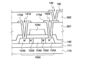
図2及び図3に示したように、透明な絶縁基板110上に酸化ケイ素または窒化ケイ素からなる遮断膜111が形成されている。
図2に示すように、画素部の遮断膜111上にはn型不純物イオンが高濃度でドーピングされているソース領域153dとドレーン領域155d及びこれらの間に位置し、不純物イオンがドーピングされないチャンネル領域154dを含む多結晶ケイ素からなる半導体層150dが形成されている。
As shown in FIGS. 2 and 3, a blocking
As shown in FIG. 2, a
また、駆動部にもn型及びp型不純物イオンが高濃度で各々ドーピングされているソース領域153n、153pとドレーン領域155n、155p及び不純物イオンがドーピングされないチャンネル領域154n、154pを各々含むNMOS及びPMOSで構成されるCMOS素子の多結晶ケイ素からなる半導体層150n、150pが各々形成されている。NMOSの場合、ソース領域153nとチャンネル領域154nとの間、ドレーン領域155nとチャンネル領域154nとの間に、n型不純物イオンが低濃度で注入されている低濃度ドーピング領域152nが各々形成されている。一方、PMOSの場合、半導体層150pのソース領域153p及びドレーン領域155pに、n型不純物イオンが低濃度で注入されている。このような低濃度のn型不純物イオンは例えば、PMOS半導体層150pの両端に含まれる。
Further, NMOS and PMOS each including
多結晶ケイ素からなる半導体層150d、150n、150pを含む基板110の上には、ゲート絶縁膜140が形成されている。このようなゲート絶縁膜140は、例えば、酸化ケイ素または窒化ケイ素の単一膜で構成することができ、酸化ケイ素と窒化ケイ素が連続的に積層された多重膜(図示せず)で構成することもできる。
ゲート絶縁膜140は、半導体層150d、150n、150p全体を覆って形成されている。このゲート絶縁膜140には、画素部の半導体層150dのソース領域153d及びドレーン領域155dと、後述するソース電極173d及びドレーン電極175dとをそれぞれ電気的に接続するための第1コンタクトホール141dおよび第2コンタクトホール142dが形成されている。
A
The
同様に、ゲート絶縁膜140には、駆動部の半導体層150nのソース領域153n及びドレーン領域155nと、ソース電極173nおよびドレーン電極175nとをそれぞれ電気的に接続するための第1コンタクトホール141n及び第2コンタクトホール142nが形成されている。さらに、ゲート絶縁膜140には、駆動部の半導体150pのソース領域153p及びドレーン領域155pと、ソース電極173n及びドレーン電極175pとをそれぞれ電気的に接続するための第1コンタクトホール141p及び第2コンタクトホール142pが形成されている。
Similarly, the
画素部のゲート絶縁膜140上には、一方向に延長されてゲート線(図示せず)が形成されており、このゲート線の一部が分岐して半導体層150d内に形成されているチャンネル領域154d及び低濃度ドーピング領域152dと重畳され、薄膜トランジスタのゲート電極124dを構成している。ゲート線の一端部分は外部回路と接続するためにゲート線より幅を拡張して形成することができ、ゲート駆動回路の出力端に直接接続するように構成できる。
On the
また、駆動部のゲート絶縁膜140上に形成されているNMOSのゲート電極124nは、半導体層150n内に形成されているチャンネル領域154n及び低濃度ドーピング領域152nと重畳されており、PMOSのゲート電極124pは半導体層150p 内に形成されているチャンネル領域154pと重畳されている。ゲート電極が低濃度ドーピング領域の少なくとも一部と重畳する構造を、GOLDD(Gate OverLapped Lightly Doped Drain)構造と言う。このようなGOLDD構造を含む薄膜トランジスタは、ソース領域のジャンクションやドレーン領域のジャンクションに印加される電界を緩和させうる。したがって、チャンネル領域内から発生する可能性がある熱電子を効果的に分散して熱電子による薄膜トランジスタの温度上昇を効果的に改善できる。
Further, the
ゲート電極124d、124n、124pが形成されている構造物上に、層間絶縁膜601が形成されている。このような第1層間絶縁膜601は、ソース領域153d、153n、153p及びドレーン領域155d、155n、155pを各々ソース電極173d、173n、173p及びドレーン電極175d、175n、175pと電気的に接続するためにゲート絶縁膜140に形成されている第1及び第2コンタクトホール141d、141n、141p、142d、142n、142pとそれぞれ連続して形成されるコンタクトホールを含む。
An interlayer insulating
画素部の第1層間絶縁膜601上には、ゲート線と交差して画素領域を定義するデータ線(図示せず)が形成されている。データ線の一部分または分岐する部分が、第1コンタクトホール141dを通じてソース領域153dと接続されている。ソース領域153dと接続されているデータ線の一部分または分岐する部分は、薄膜トランジスタのソース電極173dを構成する。このようなソース電極173と同一レベルであって、ソース電極173dと一定距離離間する位置に、第2コンタクトホール142dを通じてドレーン領域155dと接続されるドレーン電極175dが形成されている。データ線の一端部分は、外部回路と接続するためにデータ線より幅を拡張して形成(図示せず)することができ、データ駆動回路の出力端に直接接続することができる。
On the first
駆動部の第1層間絶縁膜601には、NMOSとPMOSのソース電極173n、173pが形成されて第1コンタクトホール141n、141pを通じてソース領域153n、153pにそれぞれ電気的に接続されている。また、チャンネル領域154n、154pを中心にソース電極173n、173pの反対側には、第2コンタクトホール142n、142pを通じてドレーン領域155n、155pにそれぞれ接続されているドレーン電極175n、175pが形成されている。この際、NMOS薄膜トランジスタのドレーン電極175nは、PMOS薄膜トランジスタのソース電極173pと接続される。
NMOS and
ソース電極173d、173n、173p及びドレーン電極175d、175n、175p及びデータ線が形成されている第1層間絶縁膜601上に第2層間絶縁膜602が形成されている。画素部の第2層間絶縁膜602上には、第3コンタクトホール143を通じてドレーン電極175dと接続される画素電極190が各画素領域に形成されている。
次いで、図4及び図5を参照して、多結晶ケイ素をチャンネル領域にする本発明の他の実施形態による薄膜トランジスタ基板について説明する。図4は、本発明の他の実施形態による薄膜トランジスタ基板での画素部の断面図であり、図5は、本発明の他の実施形態による薄膜トランジスタ基板でのPMOSとNMOSを有するCMOS素子の構造を示した駆動部の断面図である。
A second
A thin film transistor substrate according to another embodiment of the present invention in which polycrystalline silicon is used as a channel region will now be described with reference to FIGS. FIG. 4 is a cross-sectional view of a pixel portion of a thin film transistor substrate according to another embodiment of the present invention, and FIG. 5 illustrates a structure of a CMOS device having PMOS and NMOS in the thin film transistor substrate according to another embodiment of the present invention. It is sectional drawing of the drive part shown.
図4及び図5に示したように本発明の他の実施形態による薄膜トランジスタ基板は、画素部のゲート電極125d及びNMOSのゲート電極125nが各半導体層150d、150n内に形成されているチャンネル領域154d、154nと重畳する構造を有するということを除いては、本発明の一実施形態による薄膜トランジスタ基板と同一なので重複する説明は省略する。
前述した本発明の実施形態による薄膜トランジスタ基板の製造方法を添付した図面を参照して詳しく説明する。図6、図8、図10、図12、図14、図16、図18及び図20は、本発明の一実施形態による薄膜トランジスタ基板の画素部の各段階別工程の中間構造物の断面図であり、図7、図9、図11、図13、図15、図17、図19及び図21は、本発明の一実施形態による薄膜トランジスタ基板の駆動部の各段階別工程の中間構造物の断面図である。
4 and 5, the thin film transistor substrate according to another embodiment of the present invention includes a
A method of manufacturing the thin film transistor substrate according to the embodiment of the present invention will be described in detail with reference to the accompanying drawings. 6, 8, 10, 12, 12, 14, 16, 18 and 20 are cross-sectional views of intermediate structures in respective steps of a pixel portion of a thin film transistor substrate according to an embodiment of the present invention. 7, 9, 11, 13, 15, 17, 19, and 21 are cross-sectional views of an intermediate structure in each step of the driving part of the thin film transistor substrate according to an embodiment of the present invention FIG.
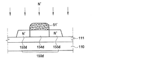
図6及び図7に示すように、まず透明な絶縁基板110上に遮断膜111を形成する。基板110としては、ガラス、石英またはサファイアなどを使用できる。基板110上に形成される遮断膜111は、基板110から遮断膜111上部に形成される半導体層150d、150n、150pに不純物などが拡散することを防止するためのもので、例えば酸化ケイ素(SiO2) または窒化ケイ素(SiNx)を蒸着して形成する。この際、遮断膜111の厚さは、例えば約5000Åの厚さに形成することができる。
As shown in FIGS. 6 and 7, first, a blocking
続いて、 遮断膜111上に非晶質ケイ素を例えば、500Åの厚さに蒸着して非晶質ケイ素層を形成する。非晶質ケイ素膜は、エキシマレーザーアニーリング(Excimer Laser Annealing;ELA)、連続側面固化(Sequential Lateral Solidification;SLS)、金属誘導結晶化(Metal Induced Crystallization;MIC)または金属誘導側面結晶化(Matal Induced Lateral Crystallization;MILC)法を使って結晶化を行い、多結晶ケイ素膜を構成する。
Subsequently, amorphous silicon is deposited on the
次に、結晶化された多結晶ケイ素膜上に感光膜を形成して、スリットマスクまたはハーフトーンマスク(図示せず)を用いて写真工程で感光膜を露光及び現像して、所定形状の感光膜パターン51,52,53を形成する。感光膜パターン51,52,53は例えば、 感光膜を所定の形状にパターニングした後、加熱収縮してその断面が台形になるようにすることもでき、融溶型感光膜を使って加熱してその断面が半球型にするなど目的するところのよって多様な形状を有するように形成できる。このような感光膜パターン51,52,53は、多結晶ケイ素膜を半導体層にパターニングするための蝕刻マスクとして使われるだけでなく、n型不純物イオンを注入するためのイオン注入マスクとしても使うことができる。
Next, a photosensitive film is formed on the crystallized polycrystalline silicon film, and the photosensitive film is exposed and developed in a photographic process using a slit mask or a halftone mask (not shown), so that a photosensitive film having a predetermined shape is obtained.
画素部の多結晶ケイ素膜上に形成された感光膜パターン51は、第1厚さ(d1)を有する高層部51aと高層部51aの両側に各々隣接した第2厚さ(d2)の低層部51b、51cを含む2層構造を有する。このような感光膜パターン51の高層部51aの幅(w1)は、半導体層(図2の150d)内に形成しようとするチャンネル領域(図2の154d)及び低濃度ドーピング領域152dの幅によって変わる。また、感光膜パターン51の全体幅(w1+w2+w3)は、形成しようとする半導体層(図2の150d)の幅によって変わる。
The
駆動部の多結晶ケイ素膜上に形成された感光膜パターン52,53のうち、NMOSの半導体層をパターニングするための感光膜パターン52は、第1厚さ(d1)を有する高層部52aと高層部52aの両側に各々隣接した第2厚さ(d2)の低層部52b、52cを含む2層構造を有し、PMOSの半導体層をパターニングするための感光膜パターン53は、第1厚さ(d1)の単層構造とすることができる。2層構造の感光膜パターン52の高層部52aの幅(w4)は、画素部と同様にNMOSの半導体層(図3の150n)内に形成しようとするチャンネル領域(図3の154n)及び低濃度ドーピング領域152nの幅によって変わる。また、2層構造の感光膜パターン52の全体幅(w4+w5+w6)は、形成しようとするNMOSの半導体層(図3の150n)の幅によって変わる。また、単層構造の感光膜パターン53の幅(w7)も形成しようとするPMOSの半導体層(図3の150p)の幅によって変わる。
Among the
引き続き、多結晶ケイ素膜上に形成された感光膜パターン51,52,53を各々蝕刻マスクとして使って、多結晶ケイ素膜をパターニングして半導体層150d、150n、150pを形成する。
次いで、図8及び図9に示したように感光膜パターン(図6の51、図7の52、53)を酸素プラズマを用いて感光膜パターン(図6の51、図7の52)の低層部(図6の51b、51c、図7の52b、52c)が所定の高さに除去されるまでアッシングする。
Subsequently, using the
Next, as shown in FIGS. 8 and 9, the photosensitive film pattern (51 in FIG. 6, 52 and 53 in FIG. 7) is formed by using oxygen plasma as the lower layer of the photosensitive film pattern (51 in FIG. Ashing is performed until the portions (51b and 51c in FIG. 6 and 52b and 52c in FIG. 7) are removed to a predetermined height.
引き続き、アッシングされた感光膜パターン51',52',53'をイオン注入マスクにして、高濃度のn型不純物イオン(N+)を画素部及びNMOSの半導体層150d、150n内に注入してソース領域153d、153n、ドレーン領域155d、155n及びチャンネル領域154d、154nを形成する。この際、チャンネル領域154d、154nは、感光膜パターン51',52'と重畳する領域に位置した半導体層150d、150nに該当して不純物イオンが注入されず、ソース領域153d、153nとドレーン領域155d、155nを分離する。
Subsequently, high-concentration n-type impurity ions (N + ) are implanted into the pixel portion and the
また、感光膜パターン53'と重畳する領域に位置するPMOSの半導体層150pには、感光膜パターン53'によって不純物イオンが注入されることが遮断される。
不純物イオン注入にPH3などを使うことができ、ドーズ量及びイオン注入エネルギーは、各素子の特性に適するように調節する。従来では、半導体層上にゲート絶縁膜が形成されている状態で高濃度のn型不純物イオン(N+)を注入したが、本発明の一実施形態による薄膜トランジスタ基板の製造方法では、半導体層に上部膜が形成されない状態で高濃度不純物イオン注入が実施されるので、相対的に低いイオン注入エネルギーによっても不純物イオンの注入が可能である。
Further, the implantation of impurity ions into the
PH 3 or the like can be used for impurity ion implantation, and the dose and ion implantation energy are adjusted to suit the characteristics of each element. Conventionally, high-concentration n-type impurity ions (N + ) are implanted in a state where a gate insulating film is formed on a semiconductor layer. However, in the method of manufacturing a thin film transistor substrate according to an embodiment of the present invention, a semiconductor layer is formed. Since high-concentration impurity ion implantation is performed in a state where the upper film is not formed, impurity ions can be implanted even with relatively low ion implantation energy.
次いで、図10及び図11に示したように感光膜パターン(図8の51'、図9の52'、53')を酸素プラズマを用いて各々の両側壁の所定部分を除去する。この際、所定部分と言うことは半導体層150d、150n内に形成しようとする低濃度ドーピング領域152d、152n,152pの幅に該当する。
引き続き、アッシングされた感光膜パターン51"',52"',53"'をイオン注入マスクにして低濃度のn型不純物イオン(N-)を半導体層150d、150n、150p内部に注入して低濃度ドーピング領域152d、152n、152pを形成する。結局、アッシングされた感光膜パターン51"',52"',53"'の両側壁は、半導体層150d、150n、150p内に形成される低濃度ドーピング領域152d、152n、152pとチャンネル領域154d、154n、154pとの境界に実質的に整列される。低濃度のn型の不純物イオン注入には、PH3などを使うことができ、ドーズ量及びイオン注入エネルギーは各素子の特性に適するように調節する。
Next, as shown in FIGS. 10 and 11, the photosensitive film pattern (51 ′ in FIG. 8, 52 ′ and 53 ′ in FIG. 9) is removed from the predetermined portions of both side walls using oxygen plasma. At this time, the predetermined portion corresponds to the width of the lightly doped
Subsequently, low concentration n-type impurity ions (N − ) are implanted into the semiconductor layers 150d, 150n, and 150p by using the ashed
この際、PMOSの半導体層150pの両端に形成されたn型の低濃度ドーピング領域152pは、後述するPMOSのソース領域(図3の153p)及びドレーン領域(図3の155p)を形成する際に、高濃度のp型不純物イオン(P+)が注入される。すなわち、PMOSの半導体層150pの低濃度ドーピング領域152pに注入されたn型不純物イオンの注入濃度より約10倍以上の濃度を有するp型不純物イオン(P+)が注入される。このようなn型不純物イオンの注入濃度とp型不純物イオンの注入濃度との差が大きいので、PMOSに形成される低濃度ドーピング領域152pは、CMOS素子特性に影響を及ぼさない。
At this time, the n-type lightly doped
次いで、図12及び図13に示したように半導体層150d、150n、150p上に形成された感光膜パターン(図10の51"'、図11の52"'、53"')を除去した後、半導体層150d、150n、150p が形成された基板110全体を覆うようにゲート絶縁膜140を形成する。ゲート絶縁膜140は、例えば酸化ケイ素または窒化ケイ素の単一膜で構成することができ、酸化ケイ素及び窒化ケイ素が連続的に積層されている多重膜(図示せず)で構成することもできる。この際、ゲート絶縁膜140は、例えば約600〜1200Åとすることができるが、これに限定されるものではない。
Next, after removing the photoresist pattern (51 "'in FIG. 10, 52"', 53 "'in FIG. 11) formed on the semiconductor layers 150d, 150n, and 150p as shown in FIGS. The
引き続き、ゲート絶縁膜140上にアルミニウム、クロム、モリブデンまたはこれらの合金からなる単一膜または多層膜を蒸着して、ゲート用導電膜を形成する。この際、ゲート用導電膜は、例えば3200Åの厚さに形成することができるが、これに限定されず、素子特性によって多様な厚さを有しうる。
次に、ゲート用導電膜上に感光膜を形成して、スリットマスクまたはハーフトーンマスク(図示せず)を用いて写真工程で感光膜を露光及び現像して、所定形状の感光膜パターン61,62,63を形成する。感光膜パターン61,62,63は、例えば感光膜を所定の形状にパターニングした後、加熱収縮してその断面が台形になるようにすることもでき、融溶型感光膜を使って加熱して、その断面が半球型にするなど目的するところによって多様な形状を有するように形成できる。このような感光膜パターン61,62,63は、ゲート用導電膜をゲート電極にパターニングするための蝕刻マスクとして使われるだけでなく、p型不純物イオンを注入するためのイオン注入マスクとしても使うこともできる。
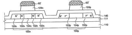
Subsequently, a single film or a multilayer film made of aluminum, chromium, molybdenum, or an alloy thereof is deposited on the
Next, a photosensitive film is formed on the gate conductive film, and the photosensitive film is exposed and developed in a photographic process using a slit mask or a halftone mask (not shown) to form a
画素部のゲート用導電膜上に形成された感光膜パターン61は、第3厚さ(d3)を有する高層部61aと高層部61aの両側に隣接する第4厚さ(d4)の低層部61b、61cを含む2層構造を有する。このような感光膜パターン61の高層部61aは、半導体層150d 内に形成されるチャンネル領域154d及び低濃度ドーピング領域152dと重畳し、低層部61b、61c はそれぞれ半導体層150d内に形成されるソース領域153d及びドレーン領域155dと重畳する。
The
駆動部のゲート用導電膜上に形成された感光膜パターン62,63のうち、NMOSの半導体層150nと重畳して形成される感光膜パターン62は、第3厚さ(d3)を有する高層部62aと高層部62aの両側に隣接した第4厚さ(d4)の低層部62b、62cを含む2層構造を有し、PMOSの半導体層150pの一部と重畳する感光膜パターン63は、第3厚さ(d3)の単層構造で構成される。
2層構造の感光膜パターン62の高層部62aは、NMOSの半導体層150n内に形成されるチャンネル領域154n及び低濃度ドーピング領域152nと重畳する。また、単層構造の感光膜パターン63は、PMOSの半導体層150p内に形成しようとする最終的なチャンネル領域154pの幅によって変わる。
Of the
The high layer portion 62a of the
引き続き、ゲート用導電膜上に形成された感光膜パターン61,62,63を各々蝕刻マスクにしてゲート用導電膜をパターニングして、画素部ではゲートパターン120dを形成し、駆動部ではNMOSのゲートパターン120n及びPMOSのゲート電極124pを形成する。この際、ゲートパターン120d、120n及びゲート電極124pの側壁は、以後に形成される上部膜との密着性を増加させるために傾斜を有するテーパー構造に形成できる。
Subsequently, the gate conductive film is patterned using each of the
次に、前述したような結果物をイオン注入マスクとして使って、高濃度のp型不純物イオン(P+)をPMOSの半導体層150p内に注入してソース領域153p及びドレーン領域155pを形成する。画素部の半導体層150dは、上部に形成された2層構造の感光膜パターン61によって不純物イオンが注入されることが遮断され、駆動部のNMOSの半導体層150n及びPMOSの半導体層150p内に形成されるチャンネル領域154pも上部に各々形成されている2層構造の感光膜パターン62及び単層構造の感光膜パターン63によって不純物イオンが注入されることが遮断される。この際、不純物イオン注入にB2H6などを使うことができ、ドーズ量及びイオン注入エネルギーは各素子の特性に適するように調節する。
Next, using the resultant as described above as an ion implantation mask, high-concentration p-type impurity ions (P + ) are implanted into the
次いで、図14及び図15に示したように感光膜パターン(図12の61、図13の 62、63)を酸素プラズマを用いて感光膜パターン(図12の61、図13の62)の低層部(図12の 61b、61c、図13の62b、62c)が所定高さまで除去されるようにアッシングする。
引き続き、アッシングされた感光膜パターン61',62',63'を各々蝕刻マスクにしてゲートパターン(図12の120d、図13の120n)をパターニングして画素部及びNMOSのゲート電極124d、124nを形成する。この際、ゲート電極124d、124nは、ゲート電極124d、124nの下部に形成されている各半導体層150d、150n 内に形成されているチャンネル領域154d、154nと重畳して、その側壁は以後に形成される上部膜との密着性を増加させるために傾斜を有するテーパー構造に形成できる。
Next, as shown in FIGS. 14 and 15, the photosensitive film pattern (61 in FIG. 12, 62, 63 in FIG. 13) is converted into a lower layer of the photosensitive film pattern (61 in FIG. 12, 62 in FIG. Ashing is performed so that the parts (61b and 61c in FIG. 12, 62b and 62c in FIG. 13) are removed to a predetermined height.
Subsequently, the gate pattern (120d in FIG. 12, 120n in FIG. 13) is patterned using the ashed
次いで、図16及び図17に示したようにゲート電極124d、124n、124p上に形成された感光膜パターン(図14の61'、図15の62'、63')を除去した後、ゲート電極124d、124n、124pが形成された基板110全体を覆うように絶縁物質を積層して第1層間絶縁膜601を形成する。
以後、第1層間絶縁膜601をマスクを利用した写真蝕刻工程にパターニングして、ソース領域153n、153p及びドレーン領域155n、155pを露出する第1コンタクトホール141n、141p及び第2コンタクトホール142n、142pを形成する。
Next, as shown in FIGS. 16 and 17, after removing the photosensitive film patterns (61 ′ in FIG. 14, 62 ′ and 63 ′ in FIG. 15) formed on the
Thereafter, the first
次いで、図18及び図19に示したように第1層間絶縁膜601上にデータ線用導電膜を形成した後、マスクを利用した写真蝕刻工程にパターニングして、データ線(図示せず)とソース電極173d、173n、173p及びドレーン電極175d、175n、175pを形成する。ソース電極173n、173pは、第1コンタクトホール141n、141pを通じてソース領域153n、153pとそれぞれ接続され、ドレーン電極175n、175pは、第2コンタクトホール142n、142pを通じてドレーン領域155n、155pとそれぞれ接続される。
Next, as shown in FIGS. 18 and 19, a data line conductive film is formed on the first
次いで、図20及び図21に示したように、データ線、ソース電極173d、173n、173p及びドレーン電極175d、175n、175pが形成されている第1層間絶縁膜601上に、平坦化特性に優れ感光性(photosensitivity)を有する有機物質またはプラズマ化学気相蒸着(plasma enhanced chemical vapor deposition,PECVD)で形成されるa-Si:C:O、
a-Si:O:Fなどの低誘電率絶縁物質を積層して、第2層間絶縁膜602を形成する。以後、所定のマスクを利用して、第2層間絶縁膜602を写真蝕刻工程でパターニングして、画素部のドレーン電極175dを露出する第3コンタクトホール143を形成する。
Next, as shown in FIGS. 20 and 21, the planarization characteristic is excellent on the first
A second
最後に、図2及び図3に示したように第3コンタクトホール143を含む第2層間絶縁膜602上に透明導電性物質であるインジウムチンオキシド(Indium Tin Oxide;ITO)またはインジウムジンクオキシド(Indium Zinc Oxide;IZO)などを蒸着した後、これをパターニングして画素電極190と多数の信号線を電気的に接続するための補助パッド(図示せず)を形成する。画素電極190は、第3コンタクトホール143を通じてドレーン電極175dと接続される。補助パッドは、第1層間絶縁膜601及び第2層間絶縁膜602にかけて形成されている第4コンタクトホール(図示せず)は、第1層間絶縁膜601及び第2層間絶縁膜602とゲート絶縁膜140にかけて形成されている第5コンタクトホール(図示せず)を通じて各々データ線及びゲート線に電気的に接続されている連結部と接続する。
Finally, as shown in FIGS. 2 and 3, a transparent conductive material such as indium tin oxide (ITO) or indium zinc oxide (Indium) is formed on the second
以下、本発明の他の実施形態による薄膜トランジスタ基板の製造方法を説明する。本発明の他の実施形態による薄膜トランジスタ基板の製造方法は、画素部のゲート電極と駆動部のNMOSのゲート電極が各々の半導体層内に形成されるチャンネル領域と重畳するように形成するということを除いては、本発明の一実施形態による薄膜トランジスタ基板の製造方法と同一なので、図4〜図11、図22〜図31を参照して、本発明の一実施形態との差を中心に説明する。図22、図24、図26、図28及び図30は、本発明の他の実施形態による薄膜トランジスタ基板の画素部の各段階別工程の中間構造物の断面図であり、図23、図25、図27、図29及び図31は、本発明の他の実施形態による薄膜トランジスタ基板の駆動部の各段階別工程の中間構造物の断面図である。 Hereinafter, a method of manufacturing a thin film transistor substrate according to another embodiment of the present invention will be described. A method of manufacturing a thin film transistor substrate according to another embodiment of the present invention includes forming a gate electrode of a pixel unit and an NMOS gate electrode of a driving unit so as to overlap with a channel region formed in each semiconductor layer. Except for this, it is the same as the method of manufacturing the thin film transistor substrate according to the embodiment of the present invention, so that the difference from the embodiment of the present invention will be mainly described with reference to FIGS. . 22, FIG. 24, FIG. 26, FIG. 28 and FIG. 30 are cross-sectional views of intermediate structures of respective steps of a pixel portion of a thin film transistor substrate according to another embodiment of the present invention. 27, 29, and 31 are cross-sectional views of an intermediate structure in each step of a driving unit of a thin film transistor substrate according to another embodiment of the present invention.
まず、図6〜図11に示したような工程により、透明絶縁基板110上に遮断膜111が形成されており、画素部及び駆動部のNMOSの遮断膜111上には、チャンネル領域154d、154nの両側に各々n型の不純物イオンが低濃度で注入されている低濃度ドーピング領域152d、152nが形成されており、このような低濃度ドーピング領域152d、152nとそれぞれ接続してn型の不純物イオンが高濃度で注入されているソース領域153d、153n及びドレーン領域155d、155nをそれぞれ含む半導体層150d、150nが形成されている。
First, the blocking
また、駆動部のPMOSの遮断膜111上には、チャンネル領域154pの両側にそれぞれp型の不純物イオンが高濃度で注入されているソース領域153p及びドレーン領域155pが形成されており、このようなソース領域153p及びドレーン領域155pとそれぞれ接続してn型の不純物イオンが低濃度でドーピングされている低濃度ドーピング領域152pを含む半導体層150pが形成されている。
Further, on the
次いで、図22に示したように半導体層150d、150n、150pが形成された基板110全体を覆うようにゲート絶縁膜140及びゲート用導電膜を順に形成する。
続いて、ゲート用導電膜導上に感光膜を形成して、スリットマスクまたはハーフトーンマスク(図示せず)を用いて写真工程で感光膜を露光及び現像して、所定形状の感光膜パターン71,72,73を形成する。
Next, as illustrated in FIG. 22, a
Subsequently, a photosensitive film is formed on the conductive film for gate, and the photosensitive film is exposed and developed in a photographic process using a slit mask or a halftone mask (not shown) to form a
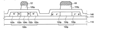
画素部のゲート用導電膜上に形成された感光膜パターン71は、第3厚さ(d3)を有する高層部71aと高層部71aの両側に隣接した第4厚さ(d4)の低層部71b、71cを含む2層構造を有する。このような感光膜パターン71の高層部71aは、半導体層150d内に形成されるチャンネル領域154dと重畳して、低層部71b、71cはそれぞれ半導体層150d 内に形成される低濃度ドーピング領域152d、ソース領域153d及びドレーン領域155dと重畳する。
The
駆動部のゲート用導電膜上に形成された感光膜パターン72,73のうち、NMOSの半導体層150nと重畳して形成される感光膜パターン72は、第3厚さ(d3)を有する高層部72aと高層部72aの両側に隣接した第4厚さ(d4)の低層部72b、72cを含む2層構造を有し、PMOSの半導体層150pの一部と重畳する感光膜パターン73は、第3厚さ(d3)を有する高層部を含む単層構造を有する。2層構造の感光膜パターン72の高層部72aは、NMOSの半導体層150n内に形成されるチャンネル領域154nと重畳して、低層部72b、72cはそれぞれ半導体層150n内に形成される低濃度ドーピング領域152n、ソース領域153n及びドレーン領域155nと重畳する。また、単層構造の感光膜パターン63は、PMOSの半導体層150p内に形成しようとする最終的なチャンネル領域154pの幅によって変わる。
Of the
続いて、ゲート用導電膜上に形成された感光膜パターン71,72,73を蝕刻マスクにしてゲート用導電膜をパターニングして、画素部ではゲートパターン120dを形成し、駆動部ではNMOSのゲートパターン120n及びPMOSのゲート電極124pを形成する。この際、ゲートパターン120d、120n及びゲート電極124pの側壁は、以後に形成される上部膜との密着性を増加させるために傾斜を有するテーパー構造に形成できる。
Subsequently, the gate conductive film is patterned using the
次に、前述したような結果物をイオン注入マスクとして使って、高濃度のp型不純物イオン(P+)をPMOSの半導体層150pに注入してソース領域153pとドレーン領域153pとを形成する。
次いで、図24及び図25に示したように感光膜パターン(図22の71、図23の72、73)を酸素プラズマを用いて感光膜パターン(図22の71、図23の72)の低層部(図22の 71b、71c、図23の72b、72c)が所定高さまで除去されるようにアッシングする。
Next, using the resultant as described above as an ion implantation mask, high-concentration p-type impurity ions (P + ) are implanted into the
Next, as shown in FIG. 24 and FIG. 25, the photosensitive film pattern (71 in FIG. 22, 72, 73 in FIG. 23) is a low layer of the photosensitive film pattern (71 in FIG. 22, 72 in FIG. Ashing is performed so that the parts (71b and 71c in FIG. 22 and 72b and 72c in FIG. 23) are removed to a predetermined height.
続いて、アッシングされた感光膜パターン71',72',73'をそれぞれ蝕刻マスクとして使って、ゲートパターン(図22の120d、図23の120n)をパターニングして画素部及びNMOSのゲート電極125d、125nを形成する。この際、ゲート電極125d、125nは、ゲート電極125d、125nの下部に形成されている各半導体層150d、150n内に形成されているチャンネル領域154d、154nと重畳して、その側壁は以後に形成される上部膜との密着性を増加させるために傾斜を有するテーパー構造に形成できる。
Subsequently, using the ashed
次いで、図26及び図27に示したように感光膜パターン(図24の71'、図25の 72'、73')が除去されたゲート電極125d、125n、124p上に第1層間絶縁膜601を形成した後、第1コンタクトホール141n、141p及び第2コンタクトホール142n、142pを形成する。
次いで、図28及び図29に示したように第1層間絶縁膜601上にデータ用導電膜を形成した後、これをパターニングしてデータ線(図示せず)と第1コンタクトホール141n、141pを通じてソース領域153n、153pと電気的に接続されるソース電極173d、173n、173p及び第2コンタクトホール142n、142pを通じてドレーン領域155n、155pと電気的に接続されるドレーン電極175d、175n、175pを形成する。
Next, as shown in FIGS. 26 and 27, the first
Next, as shown in FIGS. 28 and 29, a data conductive film is formed on the first
次いで、図30及び図31に示したようにデータ線、ソース電極173d、173n、173p及びドレーン電極175d、175n、175pが形成されている第1層間絶縁膜601上に第2層間絶縁膜602を形成した後、これをパターニングして画素部のドレーン電極175dを露出する第3コンタクトホール143を形成する。
最後に、図4及び図5に示したように第3コンタクトホール143を含む第2層間絶縁膜602上にインジウムチンオキシドまたはインジウムジンクオキシドなどを蒸着した後、これをパターニングして画素電極190と多数の信号線を電気的に接続するための補助パッド(図示せず)を形成する。
Next, as shown in FIGS. 30 and 31, a second
Finally, as shown in FIGS. 4 and 5, after depositing indium tin oxide, indium zinc oxide or the like on the second
本明細書では、画素部及びNMOSの半導体層の低濃度ドーピング領域、ソース領域及びドレーン領域には、n型不純物イオンを注入して、PMOSの半導体層のソース領域及びドレーン領域には、p型不純物イオンを注入する場合について説明したが、これは例示的なものに過ぎず、各々反対の導電型不純物イオン、すなわちp型不純物イオンを注入する場合についても適用可能であるということは言うまでもない。 In this specification, n-type impurity ions are implanted into the lightly doped region, the source region, and the drain region of the pixel portion and the NMOS semiconductor layer, and the p-type is implanted into the source region and the drain region of the PMOS semiconductor layer. Although the case of implanting impurity ions has been described, this is merely an example, and it goes without saying that the present invention can also be applied to the case of implanting opposite conductivity type impurity ions, that is, p-type impurity ions.
以上、添付された図面を参照して、本発明の実施形態を説明したが、当業者ならば本発明がその技術的思想や必須な特徴を変更せずとも、他の具体的な形態に実施できるということを理解できるであろう。したがって、前述した実施形態は、あらゆる面で例示的なものであり、限定的ではないと理解せねばならない。 The embodiments of the present invention have been described above with reference to the accompanying drawings. However, those skilled in the art can implement the present invention in other specific forms without changing the technical idea and the essential features. You will understand that you can. Accordingly, it should be understood that the above-described embodiments are illustrative in all aspects and are not limiting.
本発明の薄膜トランジスタ基板の製造方法は、工程単純化を通じる収率の改善及び原価節減に效果的であり、また、GOLDD構造の薄膜トランジスタ製造工程において追加工程を省略できる。 The method of manufacturing a thin film transistor substrate according to the present invention is effective in improving yield and cost reduction through process simplification, and can omit an additional step in the manufacturing process of a thin film transistor having a GOLDD structure.
110:基板 150d,150n,150p:半導体層
150n:低濃度ドーピング領域 153d,153n,153p:ソース領域
154d,154n,154p:チャンネル領域 155d,155n,155p:ドレーン領域
140:ゲート絶縁膜
110:
Claims (6)
前記基板上にゲート絶縁膜及び導電膜を順に形成した後、前記導電膜をパターニングしてゲート電極を形成する段階と、
を含み、
前記基板を提供する段階は、
多結晶ケイ素膜が形成されている基板上に、前記半導体層の前記チャンネル領域及び前記低濃度ドーピング領域と重畳する高層部及び前記高層部の両側にそれぞれ隣接して、前記半導体層の前記ソース/ドレーン領域とそれぞれ重畳する低層部を含む感光膜パターンを形成する段階と、
前記感光膜パターンを蝕刻マスクとして使って、前記多結晶ケイ素膜をパターニングして前記半導体層を形成する段階と、
前記感光膜パターンの前記低層部を除去して第1イオン注入マスク構造を形成する段階と、
前記第1イオン注入マスク構造をイオン注入マスクとして使って、前記半導体層内に高濃度不純物イオンを注入して前記ソース/ドレーン領域を形成する段階と、
前記低層部が除去された前記感光膜パターンの両側壁を前記半導体層の前記低濃度ドーピング領域と前記チャンネル領域との境界に実質的に整列して、第2イオン注入マスク構造を形成する段階と、
前記第2イオン注入マスク構造をイオン注入マスクとして使って、前記半導体層内に低濃度不純物イオンを注入して前記低濃度ドーピング領域を形成する段階と、
を含むことを特徴とする薄膜トランジスタ基板の製造方法。 Providing a substrate on which a semiconductor layer including a lightly doped region adjacent to both sides of a channel region and a source / drain region adjacent to the lightly doped region is formed;
Forming a gate insulating film and a conductive film on the substrate in order, and then patterning the conductive film to form a gate electrode;
Including
Providing the substrate comprises:
On the substrate on which the polycrystalline silicon film is formed, the source layer of the semiconductor layer is adjacent to the channel region of the semiconductor layer and the high layer portion overlapping the lightly doped region and both sides of the high layer portion, respectively. Forming a photosensitive film pattern including a lower layer part overlapping with the drain region,
Using the photosensitive film pattern as an etching mask to pattern the polycrystalline silicon film to form the semiconductor layer;
Removing the lower layer portion of the photoresist pattern to form a first ion implantation mask structure;
Using the first ion implantation mask structure as an ion implantation mask to implant high-concentration impurity ions into the semiconductor layer to form the source / drain region;
Forming a second ion implantation mask structure by substantially aligning both side walls of the photoresist pattern from which the low layer portion is removed with a boundary between the lightly doped region and the channel region of the semiconductor layer; ,
Using the second ion implantation mask structure as an ion implantation mask to implant lightly doped impurity ions into the semiconductor layer to form the lightly doped region;
A method for manufacturing a thin film transistor substrate, comprising:
前記基板上にゲート絶縁膜及び導電膜を順に形成して、前記導電膜上に前記第1半導体層と重畳する感光膜パターン及び前記第2半導体層内に形成されるチャンネル領域と重畳する感光膜パターンを形成する段階と、
前記各感光膜パターンを蝕刻マスクとして使って、前記導電膜をパターニングして第1ゲートパターン及び第2ゲート電極を形成する段階と、
前記結果物をイオン注入マスクとして使って、高濃度第2不純物イオンを前記第2半導体層内に注入してソース/ドレーン領域を形成する段階と、
を含み、
前記基板を提供する段階は、
多結晶ケイ素膜が形成されている基板上に、前記第1半導体層の前記チャンネル領域及び前記第1導電型低濃度ドーピング領域と重畳する高層部及び前記高層部の両側にそれぞれ隣接して、前記第1半導体層の前記第1導電型ソース/ドレーン領域とそれぞれ重畳する低層部を含む第1感光膜パターン及び前記第2半導体層と重畳する第2感光膜パターンを形成する段階と、
前記第1及び第2感光膜パターンをそれぞれ蝕刻マスクとして使って、前記多結晶ケイ素膜をパターニングして前記第1及び第2半導体層を形成する段階と、
前記第1及び第2感光膜パターンを前記第1感光膜パターンの前記低層部が除去されるまでアッシングして、第1イオン注入マスク構造を形成する段階と、
前記第1イオン注入マスク構造をイオン注入マスクとして使って、前記第1半導体層内に高濃度の第1導電型不純物イオンを注入して前記第1第導電型ソース/ドレーン領域を形成する段階と、
前記アッシングされた第1及び第2感光膜パターンを前記アッシングされた第1感光膜パターンの両側壁が前記第1半導体層の前記第1導電型低濃度ドーピング領域と前記チャンネル領域との境界に実質的に整列するまでアッシングして、第2イオン注入マスク構造を形成する段階と、
前記第2イオン注入マスク構造をイオン注入マスクとして使って、前記第1及び第2半導体層内に低濃度の前記第1導電型不純物イオンを注入してそれぞれ前記低濃度ドーピング領域を形成する段階と、
を含むことを特徴とする薄膜トランジスタ基板の製造方法。 A first conductive type lightly doped region adjacent to both sides of the channel region, a first semiconductor layer including a first conductive type source / drain region adjacent to the first conductive type lightly doped region, and a second conductive type at both ends. Providing a substrate on which a second semiconductor layer including a lightly doped region is formed;
A gate insulating film and a conductive film are sequentially formed on the substrate, and a photosensitive film pattern overlapping with the first semiconductor layer and a photosensitive film overlapping with a channel region formed in the second semiconductor layer are formed on the conductive film. Forming a pattern; and
Patterning the conductive film using the photoresist patterns as an etching mask to form a first gate pattern and a second gate electrode;
Using the resultant as an ion implantation mask to implant high concentration second impurity ions into the second semiconductor layer to form a source / drain region;
Including
Providing the substrate comprises:
On the substrate on which the polycrystalline silicon film is formed, adjacent to both the channel region of the first semiconductor layer and the high layer portion overlapping the first conductivity type low concentration doping region and both sides of the high layer portion, Forming a first photosensitive film pattern including a lower layer part overlapping with the first conductivity type source / drain region of the first semiconductor layer and a second photosensitive film pattern overlapping with the second semiconductor layer;
Patterning the polycrystalline silicon film to form the first and second semiconductor layers using the first and second photoresist patterns as etching masks, respectively.
Ashing the first and second photoresist patterns until the lower portion of the first photoresist pattern is removed to form a first ion implantation mask structure;
Using the first ion implantation mask structure as an ion implantation mask to implant high-concentration first conductivity type impurity ions into the first semiconductor layer to form the first conductivity type source / drain region; ,
Both side walls of the ashed first and second photoresist patterns are substantially at the boundary between the first conductivity type lightly doped region and the channel region of the first semiconductor layer. Ashing until they are aligned to form a second ion implantation mask structure;
Using the second ion implantation mask structure as an ion implantation mask, implanting the low-concentration first conductivity type impurity ions into the first and second semiconductor layers to form the low-concentration doping regions, respectively; ,
A method for manufacturing a thin film transistor substrate, comprising:
Applications Claiming Priority (2)
| Application Number | Priority Date | Filing Date | Title |
|---|---|---|---|
| KR10-2005-0075690 | 2005-08-18 | ||
| KR1020050075690A KR101267499B1 (en) | 2005-08-18 | 2005-08-18 | Method for fabricating thin film transistor plate and thin film transistor plate fabricated by the same |
Publications (3)
| Publication Number | Publication Date |
|---|---|
| JP2007053356A JP2007053356A (en) | 2007-03-01 |
| JP2007053356A5 JP2007053356A5 (en) | 2009-09-10 |
| JP5399608B2 true JP5399608B2 (en) | 2014-01-29 |
Family
ID=37738104
Family Applications (1)
| Application Number | Title | Priority Date | Filing Date |
|---|---|---|---|
| JP2006209726A Expired - Fee Related JP5399608B2 (en) | 2005-08-18 | 2006-08-01 | Method for manufacturing thin film transistor substrate |
Country Status (5)
| Country | Link |
|---|---|
| US (1) | US7759178B2 (en) |
| JP (1) | JP5399608B2 (en) |
| KR (1) | KR101267499B1 (en) |
| CN (1) | CN1917155B (en) |
| TW (1) | TWI434419B (en) |
Families Citing this family (31)
| Publication number | Priority date | Publication date | Assignee | Title |
|---|---|---|---|---|
| KR101343435B1 (en) * | 2006-08-09 | 2013-12-20 | 삼성디스플레이 주식회사 | Method of making a array substrate and array substrate made by the method |
| KR100796609B1 (en) * | 2006-08-17 | 2008-01-22 | 삼성에스디아이 주식회사 | Fabricating method for cmos thin film transistor and cmos thin film transistor using the same |
| KR101752400B1 (en) | 2010-09-03 | 2017-06-30 | 삼성디스플레이 주식회사 | Method of forming polycrystalline silicon layer and thin film transistor and organic light emitting device including the polycrystalline silicon layer |
| JP5807352B2 (en) * | 2011-03-18 | 2015-11-10 | セイコーエプソン株式会社 | Manufacturing method of semiconductor device and manufacturing method of electro-optical device |
| US20140051238A1 (en) * | 2011-05-09 | 2014-02-20 | Sharp Kabushiki Kaisha | Method for producing semiconductor device |
| TWI419336B (en) * | 2011-08-26 | 2013-12-11 | Au Optronics Corp | Semiconductor device and method of making the same |
| KR101856221B1 (en) * | 2011-09-20 | 2018-05-09 | 엘지디스플레이 주식회사 | Method of fabricating a thin film transistor and method of fabricating an organic light-emitting display device |
| CN103165482B (en) * | 2011-12-13 | 2015-06-17 | 颀邦科技股份有限公司 | Bump technology |
| TW201413825A (en) * | 2012-09-17 | 2014-04-01 | Ying-Jia Xue | Method of producing thin film transistor |
| CN104701175A (en) * | 2013-12-10 | 2015-06-10 | 昆山国显光电有限公司 | Thin-film transistor manufacturing method |
| CN103700707B (en) * | 2013-12-18 | 2018-12-11 | 京东方科技集团股份有限公司 | Thin film transistor (TFT), array substrate and preparation method thereof, display device |
| KR102060377B1 (en) * | 2014-01-27 | 2020-02-11 | 한국전자통신연구원 | A Display device, method of fabricating the same, and method of fabricating an image sensor device |
| CN104064472B (en) | 2014-06-13 | 2017-01-25 | 京东方科技集团股份有限公司 | Thin film transistor, manufacturing method thereof and display device |
| CN104409512A (en) * | 2014-11-11 | 2015-03-11 | 深圳市华星光电技术有限公司 | Low-temperature polycrystalline silicon thin-film transistor based on dual-gate structure and preparation method thereof |
| US9437435B2 (en) * | 2014-11-11 | 2016-09-06 | Shenzhen China Star Optoelectronics Technology Co., Ltd. | LTPS TFT having dual gate structure and method for forming LTPS TFT |
| CN105097668A (en) * | 2015-06-30 | 2015-11-25 | 京东方科技集团股份有限公司 | Display substrate and manufacturing method thereof and display device |
| CN105140124B (en) * | 2015-07-29 | 2018-12-11 | 武汉华星光电技术有限公司 | A kind of production method of polycrystalline SiTFT |
| CN105097552A (en) * | 2015-08-14 | 2015-11-25 | 京东方科技集团股份有限公司 | Manufacturing methods of thin film transistor and array substrate, array substrate and display device |
| CN105161459B (en) * | 2015-09-07 | 2019-01-29 | 武汉华星光电技术有限公司 | Low temperature polycrystalline silicon array substrate and preparation method thereof |
| CN105206568B (en) * | 2015-10-16 | 2018-06-05 | 京东方科技集团股份有限公司 | A kind of preparation method and its array substrate of low temperature polycrystalline silicon tft array substrate |
| CN105470197B (en) * | 2016-01-28 | 2018-03-06 | 武汉华星光电技术有限公司 | The preparation method of low temperature polycrystalline silicon array base palte |
| CN106024633A (en) * | 2016-06-23 | 2016-10-12 | 京东方科技集团股份有限公司 | Preparation methods of thin film transistor and array substrate, array substrate and display device |
| CN106128961A (en) * | 2016-08-30 | 2016-11-16 | 深圳市华星光电技术有限公司 | A kind of manufacture method of LTPS thin film transistor (TFT) |
| CN106169473A (en) * | 2016-08-31 | 2016-11-30 | 深圳市华星光电技术有限公司 | A kind of COMS device based on LTPS and preparation method thereof |
| CN106128962B (en) * | 2016-09-08 | 2019-11-05 | 京东方科技集团股份有限公司 | A kind of thin film transistor and its manufacturing method, array substrate, display device |
| CN106449521B (en) | 2016-10-31 | 2018-06-15 | 京东方科技集团股份有限公司 | Display base plate and preparation method thereof, display device |
| CN106952824A (en) * | 2017-03-08 | 2017-07-14 | 深圳市华星光电技术有限公司 | A kind of preparation method of low-temperature polysilicon film transistor |
| CN107818948B (en) * | 2017-10-31 | 2020-04-17 | 京东方科技集团股份有限公司 | Preparation method of array substrate |
| CN108807422B (en) * | 2018-06-12 | 2020-08-04 | 武汉华星光电技术有限公司 | Array substrate manufacturing method, array substrate and display panel |
| TWI759751B (en) * | 2020-05-29 | 2022-04-01 | 逢甲大學 | Short-channel polycrystalline silicon thin film transistor and method therefor |
| CN114792694A (en) * | 2021-01-08 | 2022-07-26 | 华为技术有限公司 | Thin film transistor array substrate, preparation method thereof and display panel |
Family Cites Families (21)
| Publication number | Priority date | Publication date | Assignee | Title |
|---|---|---|---|---|
| JP2794678B2 (en) * | 1991-08-26 | 1998-09-10 | 株式会社 半導体エネルギー研究所 | Insulated gate semiconductor device and method of manufacturing the same |
| JP3621151B2 (en) * | 1994-06-02 | 2005-02-16 | 株式会社半導体エネルギー研究所 | Method for manufacturing semiconductor device |
| TW374196B (en) * | 1996-02-23 | 1999-11-11 | Semiconductor Energy Lab Co Ltd | Semiconductor thin film and method for manufacturing the same and semiconductor device and method for manufacturing the same |
| JP3659005B2 (en) | 1998-07-31 | 2005-06-15 | 日産自動車株式会社 | Fuel tank evaporative fuel treatment device |
| US6512271B1 (en) * | 1998-11-16 | 2003-01-28 | Semiconductor Energy Laboratory Co., Ltd. | Semiconductor device |
| US6518594B1 (en) * | 1998-11-16 | 2003-02-11 | Semiconductor Energy Laboratory Co., Ltd. | Semiconductor devices |
| US6277679B1 (en) * | 1998-11-25 | 2001-08-21 | Semiconductor Energy Laboratory Co., Ltd. | Method of manufacturing thin film transistor |
| JP4578609B2 (en) * | 1999-03-19 | 2010-11-10 | 株式会社半導体エネルギー研究所 | Electro-optic device |
| JP4115654B2 (en) * | 1999-04-30 | 2008-07-09 | 株式会社半導体エネルギー研究所 | Method for manufacturing semiconductor device |
| KR100355713B1 (en) * | 1999-05-28 | 2002-10-12 | 삼성전자 주식회사 | Top gate type TFT LCD and Method of forming it |
| JP4627822B2 (en) * | 1999-06-23 | 2011-02-09 | 株式会社半導体エネルギー研究所 | Display device |
| TW541605B (en) * | 2000-07-07 | 2003-07-11 | Hitachi Ltd | Fabrication method of semiconductor integrated circuit device |
| JP4954401B2 (en) * | 2000-08-11 | 2012-06-13 | 株式会社半導体エネルギー研究所 | Manufacturing method of semiconductor device |
| JP2002134756A (en) * | 2000-10-26 | 2002-05-10 | Matsushita Electric Ind Co Ltd | Semiconductor device and manufacturing method therefor |
| JP4312420B2 (en) * | 2001-05-18 | 2009-08-12 | 株式会社半導体エネルギー研究所 | Semiconductor device and manufacturing method thereof |
| JP2003282880A (en) * | 2002-03-22 | 2003-10-03 | Hitachi Displays Ltd | Display |
| TW579604B (en) * | 2002-12-17 | 2004-03-11 | Ind Tech Res Inst | Method of forming a top-gate type thin film transistor device |
| KR100585410B1 (en) * | 2003-11-11 | 2006-06-07 | 엘지.필립스 엘시디 주식회사 | Method for switching and driving device for liquid crystal display device with driving circuit |
| JP4321486B2 (en) * | 2004-07-12 | 2009-08-26 | セイコーエプソン株式会社 | Semiconductor device and manufacturing method of semiconductor device |
| KR101153297B1 (en) * | 2004-12-22 | 2012-06-07 | 엘지디스플레이 주식회사 | Liquid crystal display device and method of fabricating the same |
| KR101239889B1 (en) * | 2005-08-13 | 2013-03-06 | 삼성디스플레이 주식회사 | Thin film transistor plate and method of fabricating the same |
-
2005
- 2005-08-18 KR KR1020050075690A patent/KR101267499B1/en active IP Right Grant
-
2006
- 2006-07-04 TW TW095124361A patent/TWI434419B/en not_active IP Right Cessation
- 2006-08-01 JP JP2006209726A patent/JP5399608B2/en not_active Expired - Fee Related
- 2006-08-03 CN CN2006101092561A patent/CN1917155B/en not_active Expired - Fee Related
- 2006-08-18 US US11/506,740 patent/US7759178B2/en active Active
Also Published As
| Publication number | Publication date |
|---|---|
| TWI434419B (en) | 2014-04-11 |
| US7759178B2 (en) | 2010-07-20 |
| JP2007053356A (en) | 2007-03-01 |
| CN1917155A (en) | 2007-02-21 |
| CN1917155B (en) | 2010-12-22 |
| KR20070021436A (en) | 2007-02-23 |
| KR101267499B1 (en) | 2013-05-31 |
| TW200715562A (en) | 2007-04-16 |
| US20070040174A1 (en) | 2007-02-22 |
Similar Documents
| Publication | Publication Date | Title |
|---|---|---|
| JP5399608B2 (en) | Method for manufacturing thin film transistor substrate | |
| JP5348362B2 (en) | Method for manufacturing thin film transistor substrate | |
| JP5144903B2 (en) | Method for manufacturing thin film transistor substrate | |
| US8309960B2 (en) | Display device | |
| JP4546444B2 (en) | Liquid crystal display device and manufacturing method thereof | |
| KR101710179B1 (en) | Flat panel display apparatus and manufacturing method of the same | |
| US9024323B2 (en) | Array substrate and method of fabricating the same | |
| JP5138276B2 (en) | Manufacturing method of display device | |
| KR101006439B1 (en) | Method for manufacturing of Thin film transistor array panel | |
| JP2006093714A (en) | Thin-film transistor display panel, and method of manufacturing the same | |
| KR101226975B1 (en) | Array substrate for liquid crystal display device with driving circuit and method for fabricating of the same | |
| KR101224049B1 (en) | Method of fabricating liquid crystal display device | |
| KR20060028072A (en) | Thin film transistor array panel and method for manufacturing the same | |
| US11081507B2 (en) | Semiconductor device and method for manufacturing same | |
| JP2009200528A (en) | Thin film transistor device, and manufacturing method thereof | |
| US11121262B2 (en) | Semiconductor device including thin film transistor and method for manufacturing the same | |
| KR20060028520A (en) | Thin film transistor array panel and method for manufacturing the same | |
| KR20070002778A (en) | Thin film transistor plate and method of fabricating the same | |
| KR20050063014A (en) | Thin film transistor array panel and method for manufacturing the same | |
| JP2005345972A (en) | Method for manufacturing active matrix liquid crystal display | |
| KR20060028073A (en) | Thin film transistor array panel and method for manufacturing the same | |
| KR20050117055A (en) | Thin film transistor array panel and method for manufacturing the same | |
| KR20130021285A (en) | Method of manufacturing a thin film transistor and method of manufacturing a display device | |
| KR20050058822A (en) | Thin film transistor array panel, and manufacturing method thereof |
Legal Events
| Date | Code | Title | Description |
|---|---|---|---|
| A521 | Request for written amendment filed |
Free format text: JAPANESE INTERMEDIATE CODE: A523 Effective date: 20090727 |
|
| A621 | Written request for application examination |
Free format text: JAPANESE INTERMEDIATE CODE: A621 Effective date: 20090727 |
|
| A521 | Request for written amendment filed |
Free format text: JAPANESE INTERMEDIATE CODE: A523 Effective date: 20100705 |
|
| A131 | Notification of reasons for refusal |
Free format text: JAPANESE INTERMEDIATE CODE: A131 Effective date: 20120821 |
|
| A977 | Report on retrieval |
Free format text: JAPANESE INTERMEDIATE CODE: A971007 Effective date: 20120823 |
|
| A521 | Request for written amendment filed |
Free format text: JAPANESE INTERMEDIATE CODE: A523 Effective date: 20121002 |
|
| RD02 | Notification of acceptance of power of attorney |
Free format text: JAPANESE INTERMEDIATE CODE: A7422 Effective date: 20121002 |
|
| A711 | Notification of change in applicant |
Free format text: JAPANESE INTERMEDIATE CODE: A712 Effective date: 20121213 |
|
| A521 | Request for written amendment filed |
Free format text: JAPANESE INTERMEDIATE CODE: A523 Effective date: 20130322 |
|
| A131 | Notification of reasons for refusal |
Free format text: JAPANESE INTERMEDIATE CODE: A131 Effective date: 20130409 |
|
| A521 | Request for written amendment filed |
Free format text: JAPANESE INTERMEDIATE CODE: A523 Effective date: 20130520 |
|
| TRDD | Decision of grant or rejection written | ||
| A01 | Written decision to grant a patent or to grant a registration (utility model) |
Free format text: JAPANESE INTERMEDIATE CODE: A01 Effective date: 20131008 |
|
| A61 | First payment of annual fees (during grant procedure) |
Free format text: JAPANESE INTERMEDIATE CODE: A61 Effective date: 20131024 |
|
| R150 | Certificate of patent or registration of utility model |
Ref document number: 5399608 Country of ref document: JP Free format text: JAPANESE INTERMEDIATE CODE: R150 Free format text: JAPANESE INTERMEDIATE CODE: R150 |
|
| R250 | Receipt of annual fees |
Free format text: JAPANESE INTERMEDIATE CODE: R250 |
|
| R250 | Receipt of annual fees |
Free format text: JAPANESE INTERMEDIATE CODE: R250 |
|
| R250 | Receipt of annual fees |
Free format text: JAPANESE INTERMEDIATE CODE: R250 |
|
| R250 | Receipt of annual fees |
Free format text: JAPANESE INTERMEDIATE CODE: R250 |
|
| R250 | Receipt of annual fees |
Free format text: JAPANESE INTERMEDIATE CODE: R250 |
|
| LAPS | Cancellation because of no payment of annual fees |