JP5337714B2 - Euv投影露光装置 - Google Patents
Euv投影露光装置 Download PDFInfo
- Publication number
- JP5337714B2 JP5337714B2 JP2009549381A JP2009549381A JP5337714B2 JP 5337714 B2 JP5337714 B2 JP 5337714B2 JP 2009549381 A JP2009549381 A JP 2009549381A JP 2009549381 A JP2009549381 A JP 2009549381A JP 5337714 B2 JP5337714 B2 JP 5337714B2
- Authority
- JP
- Japan
- Prior art keywords
- mirror
- facet
- projection exposure
- exposure apparatus
- facets
- Prior art date
- Legal status (The legal status is an assumption and is not a legal conclusion. Google has not performed a legal analysis and makes no representation as to the accuracy of the status listed.)
- Expired - Fee Related
Links
- 239000000463 material Substances 0.000 claims description 23
- 238000005286 illumination Methods 0.000 claims description 15
- 230000003746 surface roughness Effects 0.000 claims description 8
- 238000001816 cooling Methods 0.000 claims description 7
- 229910000679 solder Inorganic materials 0.000 claims description 6
- 229910052814 silicon oxide Inorganic materials 0.000 claims description 5
- PXHVJJICTQNCMI-UHFFFAOYSA-N Nickel Chemical compound [Ni] PXHVJJICTQNCMI-UHFFFAOYSA-N 0.000 claims description 4
- 229910000831 Steel Inorganic materials 0.000 claims description 4
- 230000008878 coupling Effects 0.000 claims description 4
- 238000010168 coupling process Methods 0.000 claims description 4
- 238000005859 coupling reaction Methods 0.000 claims description 4
- 239000010959 steel Substances 0.000 claims description 4
- 229910001374 Invar Inorganic materials 0.000 claims description 2
- 229910052782 aluminium Inorganic materials 0.000 claims description 2
- 229910052802 copper Inorganic materials 0.000 claims description 2
- 229910052759 nickel Inorganic materials 0.000 claims description 2
- 238000000034 method Methods 0.000 description 40
- 239000000758 substrate Substances 0.000 description 35
- 210000001747 pupil Anatomy 0.000 description 26
- 239000010410 layer Substances 0.000 description 25
- 238000004519 manufacturing process Methods 0.000 description 21
- 238000005498 polishing Methods 0.000 description 19
- 239000002585 base Substances 0.000 description 13
- 238000001900 extreme ultraviolet lithography Methods 0.000 description 11
- 229910052710 silicon Inorganic materials 0.000 description 11
- 230000003287 optical effect Effects 0.000 description 10
- XUIMIQQOPSSXEZ-UHFFFAOYSA-N Silicon Chemical compound [Si] XUIMIQQOPSSXEZ-UHFFFAOYSA-N 0.000 description 9
- 239000010703 silicon Substances 0.000 description 9
- 239000000243 solution Substances 0.000 description 8
- 241000264877 Hippospongia communis Species 0.000 description 6
- 238000009826 distribution Methods 0.000 description 6
- 238000012986 modification Methods 0.000 description 6
- 230000004048 modification Effects 0.000 description 6
- XEEYBQQBJWHFJM-UHFFFAOYSA-N Iron Chemical compound [Fe] XEEYBQQBJWHFJM-UHFFFAOYSA-N 0.000 description 4
- 230000008569 process Effects 0.000 description 4
- 229910004298 SiO 2 Inorganic materials 0.000 description 3
- 239000007769 metal material Substances 0.000 description 3
- 230000005855 radiation Effects 0.000 description 3
- 239000011265 semifinished product Substances 0.000 description 3
- 239000003637 basic solution Substances 0.000 description 2
- 239000011248 coating agent Substances 0.000 description 2
- 238000000576 coating method Methods 0.000 description 2
- 239000002826 coolant Substances 0.000 description 2
- 230000001419 dependent effect Effects 0.000 description 2
- 230000000694 effects Effects 0.000 description 2
- 230000001771 impaired effect Effects 0.000 description 2
- 229910052742 iron Inorganic materials 0.000 description 2
- 238000005259 measurement Methods 0.000 description 2
- 239000004065 semiconductor Substances 0.000 description 2
- 230000006978 adaptation Effects 0.000 description 1
- 239000012790 adhesive layer Substances 0.000 description 1
- 238000003491 array Methods 0.000 description 1
- 230000008901 benefit Effects 0.000 description 1
- 230000005540 biological transmission Effects 0.000 description 1
- 230000015572 biosynthetic process Effects 0.000 description 1
- 230000008859 change Effects 0.000 description 1
- 230000006835 compression Effects 0.000 description 1
- 238000007906 compression Methods 0.000 description 1
- 238000007796 conventional method Methods 0.000 description 1
- 239000013078 crystal Substances 0.000 description 1
- 230000002950 deficient Effects 0.000 description 1
- 238000013461 design Methods 0.000 description 1
- 230000006866 deterioration Effects 0.000 description 1
- 238000011161 development Methods 0.000 description 1
- 230000018109 developmental process Effects 0.000 description 1
- 230000003628 erosive effect Effects 0.000 description 1
- 208000028333 fixed pupil Diseases 0.000 description 1
- 238000003384 imaging method Methods 0.000 description 1
- 229910052738 indium Inorganic materials 0.000 description 1
- APFVFJFRJDLVQX-UHFFFAOYSA-N indium atom Chemical compound [In] APFVFJFRJDLVQX-UHFFFAOYSA-N 0.000 description 1
- 238000005304 joining Methods 0.000 description 1
- 238000001459 lithography Methods 0.000 description 1
- 238000003754 machining Methods 0.000 description 1
- 239000002184 metal Substances 0.000 description 1
- 229910052751 metal Inorganic materials 0.000 description 1
- 238000003801 milling Methods 0.000 description 1
- 229910052750 molybdenum Inorganic materials 0.000 description 1
- 238000012545 processing Methods 0.000 description 1
- 208000022749 pupil disease Diseases 0.000 description 1
- 230000009467 reduction Effects 0.000 description 1
- 238000002310 reflectometry Methods 0.000 description 1
- 238000007493 shaping process Methods 0.000 description 1
- 239000007787 solid Substances 0.000 description 1
- 238000012546 transfer Methods 0.000 description 1
- XLYOFNOQVPJJNP-UHFFFAOYSA-N water Substances O XLYOFNOQVPJJNP-UHFFFAOYSA-N 0.000 description 1
Images


Classifications
-
- B—PERFORMING OPERATIONS; TRANSPORTING
- B29—WORKING OF PLASTICS; WORKING OF SUBSTANCES IN A PLASTIC STATE IN GENERAL
- B29D—PRODUCING PARTICULAR ARTICLES FROM PLASTICS OR FROM SUBSTANCES IN A PLASTIC STATE
- B29D11/00—Producing optical elements, e.g. lenses or prisms
- B29D11/00596—Mirrors
-
- G—PHYSICS
- G02—OPTICS
- G02B—OPTICAL ELEMENTS, SYSTEMS OR APPARATUS
- G02B5/00—Optical elements other than lenses
- G02B5/08—Mirrors
-
- G—PHYSICS
- G02—OPTICS
- G02B—OPTICAL ELEMENTS, SYSTEMS OR APPARATUS
- G02B5/00—Optical elements other than lenses
- G02B5/08—Mirrors
- G02B5/09—Multifaceted or polygonal mirrors, e.g. polygonal scanning mirrors; Fresnel mirrors
-
- G—PHYSICS
- G03—PHOTOGRAPHY; CINEMATOGRAPHY; ANALOGOUS TECHNIQUES USING WAVES OTHER THAN OPTICAL WAVES; ELECTROGRAPHY; HOLOGRAPHY
- G03F—PHOTOMECHANICAL PRODUCTION OF TEXTURED OR PATTERNED SURFACES, e.g. FOR PRINTING, FOR PROCESSING OF SEMICONDUCTOR DEVICES; MATERIALS THEREFOR; ORIGINALS THEREFOR; APPARATUS SPECIALLY ADAPTED THEREFOR
- G03F7/00—Photomechanical, e.g. photolithographic, production of textured or patterned surfaces, e.g. printing surfaces; Materials therefor, e.g. comprising photoresists; Apparatus specially adapted therefor
- G03F7/70—Microphotolithographic exposure; Apparatus therefor
- G03F7/70058—Mask illumination systems
- G03F7/702—Reflective illumination, i.e. reflective optical elements other than folding mirrors, e.g. extreme ultraviolet [EUV] illumination systems
-
- G—PHYSICS
- G03—PHOTOGRAPHY; CINEMATOGRAPHY; ANALOGOUS TECHNIQUES USING WAVES OTHER THAN OPTICAL WAVES; ELECTROGRAPHY; HOLOGRAPHY
- G03F—PHOTOMECHANICAL PRODUCTION OF TEXTURED OR PATTERNED SURFACES, e.g. FOR PRINTING, FOR PROCESSING OF SEMICONDUCTOR DEVICES; MATERIALS THEREFOR; ORIGINALS THEREFOR; APPARATUS SPECIALLY ADAPTED THEREFOR
- G03F7/00—Photomechanical, e.g. photolithographic, production of textured or patterned surfaces, e.g. printing surfaces; Materials therefor, e.g. comprising photoresists; Apparatus specially adapted therefor
- G03F7/70—Microphotolithographic exposure; Apparatus therefor
- G03F7/708—Construction of apparatus, e.g. environment aspects, hygiene aspects or materials
- G03F7/70808—Construction details, e.g. housing, load-lock, seals or windows for passing light in or out of apparatus
- G03F7/70825—Mounting of individual elements, e.g. mounts, holders or supports
Description
Claims (13)
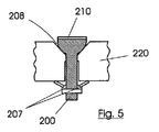
- 運搬素子(200)上に配置されたミラー素子(210)を有する投影露光装置であって、
前記ミラー素子(210)は、HSFR(High Spatial Frequency)の範囲において、表面粗さを0.5nm rms未満とすることができる、光学研磨可能な素材により構成され、
前記運搬素子(200)は、少なくとも100W/(mk)の熱伝導を有する素材により構成され、かつ、
前記ミラー素子(210)は、0.2〜5mmの厚みを有し、
溝として形成される空洞が、前記ミラー素子(210)と前記運搬素子(200)との間の領域に形成されることを特徴とする、EUV投影露光装置。 - 前記ミラー素子(210)は、前記装置の照明システム内に配置されたファセットミラーの部品として形成されたミラーファセット(210)であることを特徴とする、請求項1に記載のEUV投影露光装置。
- 前記ミラー素子(210)は、Siを含有することを特徴とする、請求項1または2に記載のEUV投影露光装置。
- 前記ミラー素子(210)は、ニッケル被覆鋼鉄体として形成されることを特徴とする、請求項1または2に記載のEUV投影露光装置。
- 前記運搬素子(200)は運搬体(220)上に配置され、前記運搬体(220)に対して可動に設けられることを特徴とする、請求項1〜4のいずれか一項に記載のEUV投影露光装置。
- 前記運搬素子(200)及び前記運搬体(220)は、同一の素材から形成されることを特徴とする、請求項5に記載のEUV投影露光装置。
- 前記運搬素子(200)は、インバー、CuまたはAl、から形成されることを特徴とする、請求項1〜6のいずれか一項に記載のEUV投影露光装置。
- 前記ミラー素子(210)及び前記運搬素子(200)は相互に半田結合で結合されることを特徴とする、請求項1〜7のいずれか一項に記載のEUV投影露光装置。
- 前記ミラー素子(210)は、前記運搬素子(200)に、シリコン酸化物ブリッジを含む無機層により結合されることを特徴とする、請求項1〜7のいずれか一項に記載のEUV投影露光装置。
- 前記空洞は、冷却線(235)に結合されることを特徴とする、請求項1〜9の何れか一項に記載のEUV投影露光装置。
- 前記ミラー素子(210)は、V字状または球状に形成されることを特徴とする、請求項1〜10のいずれか一項に記載のEUV投影露光装置。
- 前記ミラー素子(210)は、2mm〜15mmの直径を有する略環状の薄層であることを特徴とする、請求項1〜10のいずれか一項に記載のEUV投影露光装置。
- 前記ミラー素子(210)及び前記運搬素子(200)は、70MPa未満の弾性係数を有する結合素材により構成された結合層によって相互に結合されることを特徴とする、請求項1〜12のいずれか一項に記載のEUV投影露光装置。
Applications Claiming Priority (3)
| Application Number | Priority Date | Filing Date | Title |
|---|---|---|---|
| DE102007008448.1 | 2007-02-19 | ||
| DE102007008448A DE102007008448A1 (de) | 2007-02-19 | 2007-02-19 | Verfahren zur Herstellung von Spiegelfacetten für einen Facettenspiegel |
| PCT/EP2008/001247 WO2008101656A2 (en) | 2007-02-19 | 2008-02-18 | Method for producing facet mirrors and projection exposure apparatus |
Publications (2)
| Publication Number | Publication Date |
|---|---|
| JP2010519725A JP2010519725A (ja) | 2010-06-03 |
| JP5337714B2 true JP5337714B2 (ja) | 2013-11-06 |
Family
ID=39564764
Family Applications (1)
| Application Number | Title | Priority Date | Filing Date |
|---|---|---|---|
| JP2009549381A Expired - Fee Related JP5337714B2 (ja) | 2007-02-19 | 2008-02-18 | Euv投影露光装置 |
Country Status (5)
| Country | Link |
|---|---|
| US (2) | US20100007866A1 (ja) |
| EP (1) | EP2122393B1 (ja) |
| JP (1) | JP5337714B2 (ja) |
| DE (1) | DE102007008448A1 (ja) |
| WO (1) | WO2008101656A2 (ja) |
Cited By (1)
| Publication number | Priority date | Publication date | Assignee | Title |
|---|---|---|---|---|
| WO2024022899A1 (de) * | 2022-07-25 | 2024-02-01 | Carl Zeiss Smt Gmbh | Facettenspiegel-baugruppe |
Families Citing this family (21)
| Publication number | Priority date | Publication date | Assignee | Title |
|---|---|---|---|---|
| DE102008049586A1 (de) * | 2008-09-30 | 2010-04-08 | Carl Zeiss Smt Ag | Feldfacettenspiegel zum Einsatz in einer Beleuchtungsoptik einer Projektionsbelichtungsanlage für die EUV-Mikrolithographie |
| DE102008049585A1 (de) * | 2008-09-30 | 2010-04-08 | Carl Zeiss Smt Ag | Feldfacettenspiegel zum Einsatz in einer Beleuchtungsoptik einer Projektionsbelichtungsanlage für die EUV-Mikrolithographie |
| KR101769157B1 (ko) * | 2008-10-20 | 2017-08-17 | 칼 짜이스 에스엠테 게엠베하 | 방사선 빔 안내를 위한 광학 모듈 |
| DE102009025664A1 (de) | 2008-11-18 | 2010-05-20 | Carl Zeiss Smt Ag | Facettenelement zum Aufbau eines Facettenspiegels |
| DE102009006685A1 (de) | 2009-01-29 | 2010-08-05 | Carl Zeiss Smt Ag | Beleuchtungssystem für die Mikro-Lithographie |
| JP2012181220A (ja) * | 2009-07-02 | 2012-09-20 | Asahi Glass Co Ltd | ArFリソグラフィ用ミラー、およびArFリソグラフィ用光学部材 |
| DE102009054888A1 (de) * | 2009-12-17 | 2011-06-22 | Carl Zeiss SMT GmbH, 73447 | Optisches Element mit einer Mehrzahl von refletiven Facettenelementen |
| US8810775B2 (en) * | 2010-04-16 | 2014-08-19 | Media Lario S.R.L. | EUV mirror module with a nickel electroformed curved mirror |
| WO2012013227A1 (en) * | 2010-07-28 | 2012-02-02 | Carl Zeiss Smt Gmbh | Facet mirror device |
| DE102010039965B4 (de) * | 2010-08-31 | 2019-04-25 | Carl Zeiss Smt Gmbh | EUV-Kollektor |
| WO2012063852A1 (ja) * | 2010-11-09 | 2012-05-18 | 株式会社 ニコン | 反射光学部材、光学系、露光装置及びデバイスの製造方法 |
| DE102011005778A1 (de) | 2011-03-18 | 2012-09-20 | Carl Zeiss Smt Gmbh | Optisches Element |
| DE102011087323A1 (de) | 2011-11-29 | 2012-12-13 | Carl Zeiss Smt Gmbh | Zwangsgeformtes optisches Element und Verfahren zu seiner Herstellung |
| DE102011087331A1 (de) | 2011-11-29 | 2013-01-10 | Carl Zeiss Smt Gmbh | Temperaturempfindliches optisches Element aus SiSiC-Verbund und Halterung hierfür sowie Verfahren zu seiner Herstellung |
| DE102012209412A1 (de) | 2012-06-04 | 2013-12-05 | Carl Zeiss Smt Gmbh | Optisches Verfahren und optische Messvorrichtung zum Messen von Winkellagen von Facetten zumindest eines Facettenspiegels für EUV-Anwendungen |
| DE102012223754A1 (de) * | 2012-12-19 | 2014-05-15 | Carl Zeiss Smt Gmbh | Verfahren und Vorrichtung zur automatisierten Montage von Facettenspiegeln und entsprechend hergestellte Facettenspiegel |
| DE102015200531A1 (de) | 2015-01-15 | 2016-02-18 | Carl Zeiss Smt Gmbh | Optisches Modul |
| DE102015209176A1 (de) * | 2015-05-20 | 2016-11-24 | Carl Zeiss Smt Gmbh | Beleuchtungsoptik für die EUV-Projektionslithographie |
| DE102016205624B4 (de) * | 2016-04-05 | 2017-12-28 | Carl Zeiss Smt Gmbh | Beleuchtungsoptik für die EUV-Projektionslithografie, Beleuchtungssystem, Projektionsbelichtungsanlage und Verfahren zur Projektionsbelichtung |
| JP6357505B2 (ja) * | 2016-06-23 | 2018-07-11 | カール・ツァイス・エスエムティー・ゲーエムベーハー | ファセットミラーデバイス |
| EP3640687A1 (en) * | 2018-10-18 | 2020-04-22 | Essilor International | Optical article having an interferential coating with a high abrasion-resistance |
Family Cites Families (22)
| Publication number | Priority date | Publication date | Assignee | Title |
|---|---|---|---|---|
| US420265A (en) * | 1890-01-28 | Fare-box | ||
| US4202605A (en) * | 1979-04-05 | 1980-05-13 | Rockwell International Corporation | Active segmented mirror |
| JPH0772318A (ja) * | 1993-04-28 | 1995-03-17 | Canon Inc | 反射装置とこれを用いた照明装置や露光装置、並びにデバイス製造方法 |
| JPH09217039A (ja) * | 1996-02-08 | 1997-08-19 | Toshiba Corp | 無機接着剤及びそれを用いた半導体装置及びその製造方法 |
| AU3137097A (en) * | 1996-05-16 | 1997-12-05 | Lockheed Martin Energy Systems, Inc. | Low temperature material bonding technique |
| US6438199B1 (en) | 1998-05-05 | 2002-08-20 | Carl-Zeiss-Stiftung | Illumination system particularly for microlithography |
| EP0955565A3 (en) * | 1998-05-08 | 2001-05-30 | Nikon Corporation | Mirror for soft x-ray exposure apparatus |
| JP2000098114A (ja) * | 1998-09-22 | 2000-04-07 | Nikon Corp | 多光源形成反射鏡の製造方法及び該反射鏡を用いた光学装置 |
| JP2001348243A (ja) * | 2000-06-01 | 2001-12-18 | Noboru Mikami | スランピング硝子形成方法 |
| DE10030495A1 (de) | 2000-06-21 | 2002-01-03 | Zeiss Carl | Verfahren zum Verbinden einer Vielzahl von optischen Elementen mit einem Grundkörper |
| WO2002067021A1 (fr) * | 2001-02-23 | 2002-08-29 | Nikon Corporation | Reflecteur polygone, et systeme optique d'eclairage et dispositif d'exposition a semi-conducteurs utilisant le reflecteur polygone |
| US7843632B2 (en) * | 2006-08-16 | 2010-11-30 | Cymer, Inc. | EUV optics |
| WO2003040796A1 (en) * | 2001-11-09 | 2003-05-15 | Carl Zeiss Smt Ag | Tilting mirror |
| AU2002356606A1 (en) * | 2001-12-12 | 2003-06-23 | Carl Zeiss Smt Ag | Mirror facet and facetted mirror |
| DE10204249A1 (de) * | 2002-02-02 | 2003-08-14 | Zeiss Carl Smt Ag | Spiegelfacette für einen Facettenspiegel |
| JP4387198B2 (ja) * | 2002-02-09 | 2009-12-16 | カール・ツァイス・エスエムティー・アーゲー | 多数の鏡面を有する面鏡 |
| DE10302664A1 (de) * | 2003-01-24 | 2004-07-29 | Carl Zeiss Smt Ag | Verfahren zur Herstellung eines Facettenspiegels |
| US7246909B2 (en) * | 2003-01-24 | 2007-07-24 | Carl Zeiss Smt Ag | Method for the production of a facetted mirror |
| EP1642173A1 (en) | 2003-07-09 | 2006-04-05 | Carl Zeiss SMT AG | Facet mirrors and a method for producing mirror facets |
| US7522335B2 (en) * | 2004-03-29 | 2009-04-21 | Intel Corporation | Broad-angle multilayer mirror design |
| WO2006050891A2 (en) * | 2004-11-09 | 2006-05-18 | Carl Zeiss Smt Ag | A high-precision optical surface prepared by sagging from a masterpiece |
| US7591561B2 (en) * | 2005-10-13 | 2009-09-22 | Nikon Corporation | Liquid cooled mirror for use in extreme ultraviolet lithography |
-
2007
- 2007-02-19 DE DE102007008448A patent/DE102007008448A1/de not_active Withdrawn
-
2008
- 2008-02-18 WO PCT/EP2008/001247 patent/WO2008101656A2/en active Application Filing
- 2008-02-18 EP EP08707756A patent/EP2122393B1/en not_active Not-in-force
- 2008-02-18 JP JP2009549381A patent/JP5337714B2/ja not_active Expired - Fee Related
-
2009
- 2009-07-17 US US12/504,844 patent/US20100007866A1/en not_active Abandoned
-
2012
- 2012-11-21 US US13/683,138 patent/US20130100426A1/en not_active Abandoned
Cited By (1)
| Publication number | Priority date | Publication date | Assignee | Title |
|---|---|---|---|---|
| WO2024022899A1 (de) * | 2022-07-25 | 2024-02-01 | Carl Zeiss Smt Gmbh | Facettenspiegel-baugruppe |
Also Published As
| Publication number | Publication date |
|---|---|
| US20100007866A1 (en) | 2010-01-14 |
| WO2008101656A3 (en) | 2009-03-12 |
| JP2010519725A (ja) | 2010-06-03 |
| US20130100426A1 (en) | 2013-04-25 |
| DE102007008448A1 (de) | 2008-08-21 |
| EP2122393B1 (en) | 2013-04-03 |
| WO2008101656A2 (en) | 2008-08-28 |
| EP2122393A2 (en) | 2009-11-25 |
| WO2008101656A8 (en) | 2008-11-20 |
Similar Documents
| Publication | Publication Date | Title |
|---|---|---|
| JP5337714B2 (ja) | Euv投影露光装置 | |
| US6765712B2 (en) | Lithographic apparatus, device manufacturing method, and device manufactured thereby | |
| US8810775B2 (en) | EUV mirror module with a nickel electroformed curved mirror | |
| US6542224B2 (en) | Silica-based light-weight EUV lithography stages | |
| US20110043779A1 (en) | Grazing incidence collector optical systems for euv and x-ray applications | |
| WO1999026278A1 (fr) | Dispositif d'exposition, procede de fabrication associe, et procede d'exposition | |
| KR20120018085A (ko) | Uv 또는 euv 리소그래피용 광학 소자 | |
| WO2017153152A1 (en) | Multilayer reflector, method of manufacturing a multilayer reflector and lithographic apparatus | |
| NL2012204A (en) | Lithographic apparatus and method. | |
| TWI459047B (zh) | 組合反射鏡裝置、光學成像系統、與用以支撐組合反射鏡裝置之琢面元件之方法 | |
| US9645388B2 (en) | Facet mirror device | |
| US20240012334A1 (en) | Projection exposure apparatus for semiconductor lithography | |
| JP5220136B2 (ja) | 照明光学系、露光装置およびデバイス製造方法 | |
| JP7061666B2 (ja) | 半導体フォトリソグラフィで使用するためのアセンブリ及び同一のものを製造する方法 | |
| JP2013533632A5 (ja) | ||
| TW202349134A (zh) | 用於半導體微影的投影曝光設備的組件及投影曝光設備 | |
| US5975709A (en) | Reflecting system | |
| TW202311805A (zh) | 光學元件、投影光學單元及投影曝光裝置 | |
| JP2000162415A (ja) | 反射鏡の製造方法又は反射型照明装置又は半導体露光装置 | |
| JP3301249B2 (ja) | 反射用光学素子及びその製造方法 | |
| JP2023522747A (ja) | ファセットミラー用のファセットアセンブリ | |
| JP2000162414A (ja) | 反射鏡の製造方法又は反射型照明装置又は半導体露光装置 | |
| CN107003623B (zh) | 光刻系统的连接配置 | |
| US20240159988A1 (en) | Support for an optical element | |
| US20230393485A1 (en) | Optical assembly, method for deforming an optical element, and projection exposure system |
Legal Events
| Date | Code | Title | Description |
|---|---|---|---|
| A621 | Written request for application examination |
Free format text: JAPANESE INTERMEDIATE CODE: A621 Effective date: 20101008 |
|
| A977 | Report on retrieval |
Free format text: JAPANESE INTERMEDIATE CODE: A971007 Effective date: 20120620 |
|
| A131 | Notification of reasons for refusal |
Free format text: JAPANESE INTERMEDIATE CODE: A131 Effective date: 20120626 |
|
| A601 | Written request for extension of time |
Free format text: JAPANESE INTERMEDIATE CODE: A601 Effective date: 20120926 |
|
| A602 | Written permission of extension of time |
Free format text: JAPANESE INTERMEDIATE CODE: A602 Effective date: 20121003 |
|
| A521 | Request for written amendment filed |
Free format text: JAPANESE INTERMEDIATE CODE: A523 Effective date: 20121025 |
|
| TRDD | Decision of grant or rejection written | ||
| A01 | Written decision to grant a patent or to grant a registration (utility model) |
Free format text: JAPANESE INTERMEDIATE CODE: A01 Effective date: 20130716 |
|
| A61 | First payment of annual fees (during grant procedure) |
Free format text: JAPANESE INTERMEDIATE CODE: A61 Effective date: 20130805 |
|
| R150 | Certificate of patent or registration of utility model |
Ref document number: 5337714 Country of ref document: JP Free format text: JAPANESE INTERMEDIATE CODE: R150 Free format text: JAPANESE INTERMEDIATE CODE: R150 |
|
| R250 | Receipt of annual fees |
Free format text: JAPANESE INTERMEDIATE CODE: R250 |
|
| R250 | Receipt of annual fees |
Free format text: JAPANESE INTERMEDIATE CODE: R250 |
|
| R250 | Receipt of annual fees |
Free format text: JAPANESE INTERMEDIATE CODE: R250 |
|
| R250 | Receipt of annual fees |
Free format text: JAPANESE INTERMEDIATE CODE: R250 |
|
| LAPS | Cancellation because of no payment of annual fees |