JP5322467B2 - Manufacturing method of display device and manufacturing method of circuit including transistor - Google Patents
Manufacturing method of display device and manufacturing method of circuit including transistor Download PDFInfo
- Publication number
- JP5322467B2 JP5322467B2 JP2008072639A JP2008072639A JP5322467B2 JP 5322467 B2 JP5322467 B2 JP 5322467B2 JP 2008072639 A JP2008072639 A JP 2008072639A JP 2008072639 A JP2008072639 A JP 2008072639A JP 5322467 B2 JP5322467 B2 JP 5322467B2
- Authority
- JP
- Japan
- Prior art keywords
- layer
- substrate
- soi
- insulating layer
- soi layer
- Prior art date
- Legal status (The legal status is an assumption and is not a legal conclusion. Google has not performed a legal analysis and makes no representation as to the accuracy of the status listed.)
- Expired - Fee Related
Links
Images


Classifications
-
- H—ELECTRICITY
- H10—SEMICONDUCTOR DEVICES; ELECTRIC SOLID-STATE DEVICES NOT OTHERWISE PROVIDED FOR
- H10D—INORGANIC ELECTRIC SEMICONDUCTOR DEVICES
- H10D86/00—Integrated devices formed in or on insulating or conducting substrates, e.g. formed in silicon-on-insulator [SOI] substrates or on stainless steel or glass substrates
- H10D86/01—Manufacture or treatment
- H10D86/021—Manufacture or treatment of multiple TFTs
- H10D86/0214—Manufacture or treatment of multiple TFTs using temporary substrates
-
- H—ELECTRICITY
- H10—SEMICONDUCTOR DEVICES; ELECTRIC SOLID-STATE DEVICES NOT OTHERWISE PROVIDED FOR
- H10D—INORGANIC ELECTRIC SEMICONDUCTOR DEVICES
- H10D86/00—Integrated devices formed in or on insulating or conducting substrates, e.g. formed in silicon-on-insulator [SOI] substrates or on stainless steel or glass substrates
- H10D86/40—Integrated devices formed in or on insulating or conducting substrates, e.g. formed in silicon-on-insulator [SOI] substrates or on stainless steel or glass substrates characterised by multiple TFTs
- H10D86/60—Integrated devices formed in or on insulating or conducting substrates, e.g. formed in silicon-on-insulator [SOI] substrates or on stainless steel or glass substrates characterised by multiple TFTs wherein the TFTs are in active matrices
-
- H—ELECTRICITY
- H10—SEMICONDUCTOR DEVICES; ELECTRIC SOLID-STATE DEVICES NOT OTHERWISE PROVIDED FOR
- H10D—INORGANIC ELECTRIC SEMICONDUCTOR DEVICES
- H10D30/00—Field-effect transistors [FET]
- H10D30/01—Manufacture or treatment
- H10D30/021—Manufacture or treatment of FETs having insulated gates [IGFET]
- H10D30/031—Manufacture or treatment of FETs having insulated gates [IGFET] of thin-film transistors [TFT]
- H10D30/0321—Manufacture or treatment of FETs having insulated gates [IGFET] of thin-film transistors [TFT] comprising silicon, e.g. amorphous silicon or polysilicon
- H10D30/0323—Manufacture or treatment of FETs having insulated gates [IGFET] of thin-film transistors [TFT] comprising silicon, e.g. amorphous silicon or polysilicon comprising monocrystalline silicon
Landscapes
- Thin Film Transistor (AREA)
- Liquid Crystal (AREA)
- Metal-Oxide And Bipolar Metal-Oxide Semiconductor Integrated Circuits (AREA)
- Element Separation (AREA)
Abstract
Description
本発明は、SOI(Silicon on Insulator)基板及びそれにより製造される表示装置に関する。特に貼り合わせSOI技術に関するものであって、ガラス等の絶縁表面を有する基板に単結晶若しくは多結晶の半導体層を接合させたSOI基板及び当該SOI基板を用いて製造される表示装置に関する。 The present invention relates to an SOI (Silicon on Insulator) substrate and a display device manufactured thereby. In particular, the present invention relates to a bonded SOI technology, and relates to an SOI substrate in which a single crystal or polycrystalline semiconductor layer is bonded to a substrate having an insulating surface such as glass, and a display device manufactured using the SOI substrate.
近年、VLSI技術が飛躍的な進歩を遂げる中で、高速化、低消費電力化を実現できるSOI構造が注目されている。この技術は、従来バルク単結晶シリコンで形成されていた電界効果トランジスタ(FET;Field Effect Transistor)の活性領域(チャネル形成領域)を、単結晶シリコン薄膜とする技術である。SOI構造を用いてMOS型電界効果トランジスタを作製すると、従来のバルク単結晶シリコン基板を用いる場合よりも寄生容量を小さくでき、高速化に有利になることが知られている。 In recent years, an SOI structure capable of realizing high speed and low power consumption has attracted attention as VLSI technology has made great progress. This technique is a technique in which an active region (channel formation region) of a field effect transistor (FET) that has been conventionally formed of bulk single crystal silicon is a single crystal silicon thin film. It is known that when a MOS field effect transistor is manufactured using an SOI structure, the parasitic capacitance can be made smaller than when a conventional bulk single crystal silicon substrate is used, which is advantageous for high speed operation.
従来のSOI基板を製造する方法としては、水素イオン注入剥離法が知られている(例えば、特許文献1参照)。水素イオン注入剥離法は、シリコンウェハに水素イオンを注入することによって表面から所定の深さに微小気泡層を形成し、該微小気泡層を劈開面とすることで、別のシリコンウェハに薄い単結晶シリコン層(SOI層)を接合する。さらにSOI層を剥離する加熱処理を行うことに加え、酸化性雰囲気下での加熱処理によりSOI層に酸化膜を形成した後に該酸化膜を除去し、次に1000℃乃至1300℃の還元性雰囲気下で加熱処理を行って接合強度を高める必要があるとされている。 As a conventional method for manufacturing an SOI substrate, a hydrogen ion implantation separation method is known (see, for example, Patent Document 1). In the hydrogen ion implantation separation method, hydrogen ions are implanted into a silicon wafer to form a microbubble layer at a predetermined depth from the surface, and the microbubble layer is used as a cleavage plane to form a thin single wafer on another silicon wafer. A crystalline silicon layer (SOI layer) is bonded. In addition to performing heat treatment for peeling the SOI layer, an oxide film is formed on the SOI layer by heat treatment in an oxidizing atmosphere, and then the oxide film is removed, and then a reducing atmosphere at 1000 ° C. to 1300 ° C. It is said that it is necessary to increase the bonding strength by performing a heat treatment below.
SOI基板を用いた半導体装置の一例として、本出願人によるものが知られている(特許文献2参照)。この場合にも、SOI層において応力に起因する準位や欠陥を除去するために1050℃乃至1150℃の加熱処理が必要であることが開示されている。
従来のSOI基板の製造方法では、SOI層の接合強度を強固なものとするために1000℃以上の高温で加熱処理する必要があった。そのため、液晶パネル等の表示装置の製造に用いられるガラス基板のように、耐熱温度が600℃程度の基板にSOI層を形成することが困難であった。仮に水素イオン注入剥離法でSOI層をガラス基板上に設けたとしても、高温の加熱処理を適用することができないために、SOI層の接合強度が弱いといった問題があった。さらに、従来の水素イオン注入剥離法を利用したSOI基板は、1枚のシリコンウェハに対し1枚のシリコンウェハを貼りあわせてその内の1枚のシリコンウェハを薄膜化することによりSOI構造を得ていた。そのため、シリコンウェハの大きさに依存しており、大面積化を図ることは難しかった。 In a conventional method for manufacturing an SOI substrate, it is necessary to perform heat treatment at a high temperature of 1000 ° C. or higher in order to increase the bonding strength of the SOI layer. Therefore, it has been difficult to form an SOI layer on a substrate having a heat resistant temperature of about 600 ° C. like a glass substrate used for manufacturing a display device such as a liquid crystal panel. Even if the SOI layer is provided on the glass substrate by the hydrogen ion implantation separation method, there is a problem that the bonding strength of the SOI layer is weak because high-temperature heat treatment cannot be applied. Furthermore, an SOI substrate using a conventional hydrogen ion implantation separation method is obtained by bonding one silicon wafer to one silicon wafer and thinning one of the silicon wafers to obtain an SOI structure. It was. Therefore, depending on the size of the silicon wafer, it is difficult to increase the area.
上記問題に鑑み、本発明はSOI基板の大面積化を図り、当該SOI基板を用いた表示装置の製造の生産性を向上させることを目的の一とする。また、表示装置の高性能化を目的の一とする。 In view of the above problems, an object of the present invention is to increase the area of an SOI substrate and improve the productivity of manufacturing a display device using the SOI substrate. Another object is to improve the performance of the display device.
絶縁表面を有する基板上に複数の単結晶半導体層を接合させ、当該単結晶半導体層によりトランジスタを含む回路を形成して表示装置を製造することを要旨とする。 The gist is to manufacture a display device by bonding a plurality of single crystal semiconductor layers to a substrate having an insulating surface and forming a circuit including a transistor using the single crystal semiconductor layers.
当該単結晶半導体層は、単結晶半導体基板から剥離されたものが適用される。単結晶半導体基板に替えて多結晶半導体基板を適用しても良い。単結晶半導体層は、一つの表示パネルに相当する大きさ(パネルサイズ)、具体的には一のパネルを含む面積に分割され、絶縁表面を有する基板上に接合される。 As the single crystal semiconductor layer, a layer separated from a single crystal semiconductor substrate is used. A polycrystalline semiconductor substrate may be used instead of the single crystal semiconductor substrate. The single crystal semiconductor layer is divided into a size corresponding to one display panel (panel size), specifically, an area including one panel, and is bonded to a substrate having an insulating surface.
単結晶半導体基板から複数の単結晶半導体層を転置する場合には、一のアライメントマーカーに複数の単結晶半導体層が属するようにしても良い。 In the case where a plurality of single crystal semiconductor layers are transferred from a single crystal semiconductor substrate, the plurality of single crystal semiconductor layers may belong to one alignment marker.
本発明の一は、絶縁表面を有する基板上に、一のパネルを含む面積に分割された複数の単結晶半導体層を絶縁層を介して接合し、複数の単結晶半導体層から選択された一のまとまりを同時に露光して回路パターンを転写し形成することにより、個々の単結晶半導体層を用いてトランジスタを含む回路を形成する表示装置の製造方法である。 According to one embodiment of the present invention, a plurality of single crystal semiconductor layers divided into an area including one panel are joined to a substrate having an insulating surface through an insulating layer, and one selected from the plurality of single crystal semiconductor layers. This is a method for manufacturing a display device in which a circuit including a transistor is formed using individual single crystal semiconductor layers by simultaneously exposing and forming a circuit pattern to form a circuit pattern.
本発明の一は、絶縁表面を有する基板上に、一のパネルを含む面積に分割された複数の単結晶半導体層を、有機シランを原料ガスとして化学気相成長法により成膜する酸化シリコン層を介して接合し、複数の単結晶半導体層から選択された一のまとまりを同時に露光して回路パターンを転写し形成することにより、個々の単結晶半導体層を用いてトランジスタを含む回路を形成する表示装置の製造方法である。 One embodiment of the present invention is a silicon oxide layer in which a plurality of single crystal semiconductor layers divided into an area including one panel are formed on a substrate having an insulating surface by a chemical vapor deposition method using organosilane as a source gas. And forming a circuit including a transistor using each single crystal semiconductor layer by transferring and forming a circuit pattern by simultaneously exposing a group selected from a plurality of single crystal semiconductor layers. It is a manufacturing method of a display device.
また、本発明の一は、複数の単結晶半導体層から選択された一のまとまりは、露光装置で1回に露光できる範囲、つまり露光装置が1回に露光する範囲のまとまりとしてもよい。また、一のまとまりには、一のアライメントマーカーに複数の前記単結晶半導体層が属していてもよい。 Further, according to one aspect of the present invention, one group selected from a plurality of single crystal semiconductor layers may be a range that can be exposed at one time by the exposure apparatus, that is, a range that is exposed by the exposure apparatus at one time. In one unit, a plurality of single crystal semiconductor layers may belong to one alignment marker.
また、本発明の一は、絶縁表面を有する基板上にトランジスタを含む回路を有し、トランジスタに、単結晶半導体を含むチャネル形成領域を有し、トランジスタのチャネル形成領域と前記絶縁表面を有する基板との間には、有機シランを原料ガスとして化学気相成長法により成膜された酸化シリコン層が設けられている表示装置である。 Another embodiment of the present invention includes a circuit including a transistor over a substrate having an insulating surface, the transistor including a channel formation region including a single crystal semiconductor, and the substrate including the channel formation region of the transistor and the insulating surface The display device is provided with a silicon oxide layer formed by chemical vapor deposition using organosilane as a source gas.
また、本発明の一は、有機シランとしては、テトラエトキシシラン、トリメチルシラン、テトラメチルシラン、テトラメチルシクロテトラシロキサン、オクタメチルシクロテトラシロキサン、ヘキサメチルジシラザン、トリエトキシシラン、又はトリスジメチルアミノシランを用いることができる。 Further, according to one aspect of the present invention, as the organic silane, tetraethoxysilane, trimethylsilane, tetramethylsilane, tetramethylcyclotetrasiloxane, octamethylcyclotetrasiloxane, hexamethyldisilazane, triethoxysilane, or trisdimethylaminosilane is used. Can be used.
また、本発明の一は、絶縁表面を有する基板として、アルミノシリケートガラス、アルミノホウケイ酸ガラス、又はバリウムホウケイ酸ガラス、石英基板、サファイヤ基板、又はセラミック基板を用いることができる。 In one embodiment of the present invention, an aluminosilicate glass, an aluminoborosilicate glass, a barium borosilicate glass, a quartz substrate, a sapphire substrate, or a ceramic substrate can be used as the substrate having an insulating surface.
なお、本明細書において、表示装置とは、液晶素子、発光素子、又は電気泳動素子などの表示素子を用いたデバイス、すなわち画像表示デバイスを示す。また、表示パネル(液晶パネル、発光パネル)に外部入力端子、例えばフレキシブルプリント配線(FPC:Flexible Printed Circuit)もしくはTAB(Tape Automated Bonding)テープもしくはTCP(Tape Carrier Package)が取り付けられたモジュール、TABテープやTCPの先にプリント配線板が設けられたモジュール、または表示パネルにCOG(Chip On Glass)方式によりIC(集積回路)やCPU(中央演算処理装置)が直接実装されたモジュールも全て表示装置に含むものとする。 Note that in this specification, a display device refers to a device using a display element such as a liquid crystal element, a light-emitting element, or an electrophoretic element, that is, an image display device. In addition, a module in which an external input terminal such as a flexible printed circuit (FPC), a TAB (Tape Automated Bonding) tape, or a TCP (Tape Carrier Package) is attached to a display panel (liquid crystal panel, light emitting panel), a TAB tape Also, a module in which a printed wiring board is provided at the end of TCP or TCP, or a module in which an IC (Integrated Circuit) or CPU (Central Processing Unit) is directly mounted on a display panel by a COG (Chip On Glass) method Shall be included.
本発明を適用することで、SOI基板の大面積化が可能となり、当該SOI基板を用いた表示装置の製造における生産性を向上させることができる。また、SOI基板を用いた表示装置の高性能化を図ることができる。 By applying the present invention, an SOI substrate can be increased in area, and productivity in manufacturing a display device using the SOI substrate can be improved. In addition, high performance of a display device using an SOI substrate can be achieved.
本発明の実施の形態について、図面を用いて以下に説明する。但し、本発明は以下の説明に限定されず、本発明の趣旨及びその範囲から逸脱することなく、その形態及び詳細を様々に変更しうることは、当業者であれば容易に理解される。したがって、本発明は以下に示す実施の形態の記載内容に限定して解釈されるものではない。なお、以下に説明する本発明の構成において、同じものを指す符号は異なる図面間で共通して用いる場合がある。 Embodiments of the present invention will be described below with reference to the drawings. However, the present invention is not limited to the following description, and it is easily understood by those skilled in the art that modes and details can be variously changed without departing from the spirit and scope of the present invention. Therefore, the present invention should not be construed as being limited to the description of the embodiments below. Note that in the structures of the present invention described below, the same reference numerals may be used in common in different drawings.
(実施の形態1)
本実施の形態に係るSOI基板は、単結晶半導体基板から、異種基板(以下、「ベース基板」ともいう)に転置して形成する。以下、本実施の形態に係るSOI基板及びその製造方法の一形態について説明する。
(Embodiment 1)
The SOI substrate according to this embodiment is formed by being transferred from a single crystal semiconductor substrate to a different substrate (hereinafter also referred to as a “base substrate”). Hereinafter, an embodiment of an SOI substrate and a manufacturing method thereof according to the present embodiment will be described.
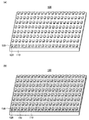
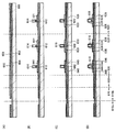
図1(A)、図1(B)に、本発明に係るSOI基板の構成を示す斜視図の例を示す。また、図2(A)、(B)及び図3(A)、(B)に、本発明に係るSOI基板の断面図の例を示す。 FIG. 1A and FIG. 1B show examples of perspective views illustrating a structure of an SOI substrate according to the present invention. 2A and 2B and FIGS. 3A and 3B show examples of cross-sectional views of an SOI substrate according to the present invention.
図1(A)及び図2(A)、(B)において、SOI基板100は、ベース基板110の一表面上に、絶縁層120及び単結晶半導体層130(以下、SOI層ともいう)が順次積層された積層体が複数設けられた構成を有する。SOI層130は、絶縁層120を介してベース基板110上に設けられており、いわゆるSOI構造を形成している。つまり、1枚のベース基板110上に複数のSOI層130が設けられて、1枚のSOI基板100を形成している。なお、図2では、便宜上1枚のベース基板110に2つのSOI層130が設けられている例を示す。
1A, 2A, and 2B, an SOI substrate 100 includes an
SOI層130は単結晶半導体であり、代表的には単結晶シリコンが適用される。その他、水素イオン注入剥離法を利用して単結晶半導体基板若しくは多結晶半導体基板から剥離可能であるシリコン、ゲルマニウムや、ガリウムヒ素、インジウムリンなどの化合物半導体である結晶性半導体層を適用することもできる。
The
本発明に係るSOI基板は、当該SOI基板を構成するSOI層130のサイズを、所望のパネルサイズとすることを特徴の1つとしている。SOI層130は、所望のパネルサイズである一のパネルを含む面積に分割されている。なお、本明細書における「パネルサイズ」とは、表示パネルの表示部及びその周辺の額縁部(非表示部)を合わせたサイズを示す。また、「サイズ」とは、面積を示すものとする。本発明に係るSOI基板は、ベース基板110上に、所望のパネルサイズである一のパネルを含む面積に分割された複数のSOI層130が絶縁層120を介して接合している。
One feature of the SOI substrate according to the present invention is that the size of the
パネルサイズは用途により適宜選択すればよいが、例えば対角10インチ未満の中小型パネルサイズとすることができる。中小型パネルとして携帯電話機を想定する場合、表示部のサイズ(画面サイズ)としては、例えば対角2.2インチ(56mm)、対角2.4インチ(61mm)、対角2.6インチ(66mm)等が知られている。これらのパネルサイズとする場合は、画面サイズに表示部周辺の額縁部のサイズ(画面額縁サイズ)を考慮したサイズとすればよい。 The panel size may be appropriately selected depending on the application, but for example, it can be a small and medium panel size of less than 10 inches diagonal. When a mobile phone is assumed as a small-to-medium-sized panel, the display unit size (screen size) is, for example, 2.2 inches diagonal (56 mm), 2.4 inches diagonal (61 mm), 2.6 inches diagonal ( 66 mm). When these panel sizes are used, the screen size may be a size that takes into account the size of the frame portion around the display portion (screen frame size).
SOI層130の形状は特に限定されないが、矩形状(正方形を含む)とすると加工が容易になり、ベース基板110にも集積度良く貼り合わせることができ好ましい。また、ディスプレイ等の表示装置のパネルとする場合は、SOI層130のアスペクト比が4:3となるようにすることが好ましい。SOI層130を所望の一のパネルを含む面積、つまり所望のパネルサイズ程度とすることで、完成するSOI基板を用いて製造した表示パネルを組み込んで各種表示装置を製造する際に、パネル毎に歩留まりを管理することが可能となる。また、個々のパネルを分断する際に、素子にダメージが入るのを防止することができる。よって、歩留まりの向上を図ることができる。さらに、SOI層130を所望の一のパネルを含む面積に分割する、つまりSOI層130を所望のパネルサイズ程度とすることで、各パネルの素子を1つのSOI層で形成することができ、特性のばらつきを抑えることが可能になる。
The shape of the
ベース基板110は絶縁表面を有する基板または絶縁基板を用いる。具体的には、アルミノシリケートガラス、アルミノホウケイ酸ガラス、バリウムホウケイ酸ガラスのような電子工業用に使われる各種ガラス基板、石英基板、セラミック基板、サファイヤ基板が挙げられる。好ましくはベース基板110としてガラス基板を用いるのがよく、例えば第6世代(1500mm×1850mm)、第7世代(1870mm×2200mm)、第8世代(2200mm×2400mm)といわれる大面積のマザーガラス基板を用いる。大面積のマザーガラス基板をベース基板110として用い、本発明を適用してSOI基板を製造することで、SOI基板の大面積化が実現できる。また、絶縁表面を有する基板であるベース基板上に、一のパネルを含む面積に分割された複数のSOI層、具体的には所望のパネルサイズに分割された複数のSOI層を絶縁層を介して接合したSOI基板は、個々のSOI層が所望のパネルサイズであるため、1枚のベース基板で製造できる表示パネルの数(面取り数)を増大させることができる。したがって、該表示パネルを組み込んで製造する最終製品(表示装置)の生産性を向上させることができる。
As the
ベース基板110とSOI層130の間には、絶縁層120が設けられている。絶縁層120は単層構造としても積層構造としてもよいが、ベース基板110と接合する面(以下、「接合面」ともいう)は、平滑面を有し親水性表面となるようにする。以下、本明細書では、接合面に形成する層を接合層ともいう。図2(A)は絶縁層120として接合層122を形成する例を示している。平滑面を有し親水性表面を形成できる接合層122としては、酸化シリコン層が適している。特に、有機シランを原料ガスに用いて化学気相成長法により作製される酸化シリコン層が好ましい。有機シランとしては、テトラエトキシシラン(略称;TEOS:化学式Si(OC2H5)4)、テトラメチルシラン(TMS:化学式Si(CH3)4)、トリメチルシラン((CH3)3SIH)、テトラメチルシクロテトラシロキサン(TMCTS)、オクタメチルシクロテトラシロキサン(OMCTS)、ヘキサメチルジシラザン(HMDS)、トリエトキシシラン(SiH(OC2H5)3)、トリスジメチルアミノシラン(SiH(N(CH3)2)3)等のシリコン含有化合物を用いることができる。
An insulating
上記平滑面を有し親水性表面を形成する接合層122は、膜厚5nm乃至500nmの範囲で設けることが好ましい。接合層122の膜厚を上記範囲内とすることで、被成膜表面の表面荒れを平滑化すると共に、当該膜の成長表面の平滑性を確保することが可能である。また、接合する基板(図2(A)ではベース基板110)との歪みを緩和することができる。なお、ベース基板110にも、接合層122と同様の酸化シリコン層を設けてもよい。本発明に係るSOI基板は、絶縁表面を有する基板若しくは絶縁基板であるベース基板110にSOI層130を接合するに際し、接合を形成する面の一方若しくは双方に、好ましくは有機シランを原料ガスとして成膜した酸化シリコン層でなる接合層を設けることで強固な接合を形成することができる。
The
図2(B)は絶縁層120を積層構造とする例を示している。具体的には、絶縁層120として接合層122及び窒素含有絶縁層124の積層構造を形成する例を示している。なお、ベース基板110との接合面には接合層122が形成されるようにするため、SOI層130と接合層122との間に窒素含有絶縁層124が設けられた構成とする。窒素含有絶縁層124は、窒化シリコン層、窒化酸化シリコン層又は酸化窒化シリコン層を用いて単層構造又は積層構造で形成する。例えば、SOI層130側から酸化窒化シリコン層、窒化酸化シリコン層を積層して窒素含有絶縁層124とすることができる。接合層122はベース基板110と接合を形成するために設けるのに対し、窒素含有絶縁層124は、可動イオンや水分等の不純物がSOI層130に拡散して汚染されることを防ぐために設けることが好ましい。
FIG. 2B illustrates an example in which the insulating
なお、酸化窒化シリコン層とは、その組成として、窒素よりも酸素の含有量が多いものを示し、ラザフォード後方散乱法(RBS:Rutherford Backscattering Spectrometry)及び水素前方散乱法(HFS:Hydrogen Forward Scattering)を用いて測定した場合に、濃度範囲として酸素が50原子%〜70原子%、窒素が0.5原子%〜15原子%、Siが25原子%〜35原子%、水素が0.1原子%〜10原子%の範囲で含まれるものをいう。また、窒化酸化シリコン層とは、その組成として、酸素よりも窒素の含有量が多いものを示し、RBS及びHFSを用いて測定した場合に、濃度範囲として酸素が5原子%〜30原子%、窒素が20原子%〜55原子%、Siが25原子%〜35原子%、水素が10原子%〜30原子%の範囲で含まれるものをいう。但し、酸化窒化シリコンまたは窒化酸化シリコンを構成する原子の合計を100原子%としたとき、窒素、酸素、Si及び水素の含有比率が上記の範囲内に含まれるものとする。 Note that the silicon oxynitride layer has a composition that contains more oxygen than nitrogen, and includes Rutherford Backscattering (RBS) and Hydrogen Forward Scattering (HFS). As a concentration range, oxygen ranges from 50 atomic% to 70 atomic%, nitrogen from 0.5 atomic% to 15 atomic%, Si from 25 atomic% to 35 atomic%, and hydrogen from 0.1 atomic% to The thing contained in the range of 10 atomic%. In addition, the silicon nitride oxide layer has a composition containing more nitrogen than oxygen, and when measured using RBS and HFS, the concentration range of oxygen is 5 atomic% to 30 atomic%, Nitrogen is included in a range of 20 atomic% to 55 atomic%, Si is included in a range of 25 atomic% to 35 atomic% and hydrogen is included in a range of 10 atomic% to 30 atomic%. However, when the total number of atoms constituting silicon oxynitride or silicon nitride oxide is 100 atomic%, the content ratio of nitrogen, oxygen, Si, and hydrogen is included in the above range.
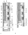
図1(B)及び図3(A)、(B)は、ベース基板110に接合層を含む絶縁層150を形成する例を示している。絶縁層150は、単層構造でも積層構造でもよいが、SOI層130との接合面は平滑面を有し親水性表面を形成するようにする。なお、ベース基板110と接合層との間には、ベース基板110として用いられるガラス基板からアルカリ金属若しくはアルカリ土類金属などの可動イオンの拡散を防ぐため、バリア層が設けられていることが好ましい。
1B and 3A and 3B illustrate an example in which an insulating
図3(A)は、絶縁層150としてバリア層152、接合層154の積層構造を形成する例を示している。接合層154としては、前記接合層122と同様の酸化シリコン層を設ければよい。また、SOI層130に適宜接合層を設けてもよい。図3(A)では、SOI層130にも接合層122を設ける例を示している。このような構成とすることで、ベース基板110及びSOI層130を接合させる際に接合層同士で接合を形成するため、より強固な接合を形成することができる。バリア層152は、酸化シリコン層、窒化シリコン層、酸化窒化シリコン層又は窒化酸化シリコン層を用いて単層構造又は積層構造で形成する。好ましくは、窒素を含有する絶縁層を用いて形成する。
FIG. 3A illustrates an example in which a stacked structure of a
図3(B)は、ベース基板110に接合層を設ける例を示している。具体的には、ベース基板110に絶縁層150としてバリア層152と接合層154の積層構造を設けている。また、SOI層130には酸化シリコン層126を設けている。ベース基板110にSOI層130を接合する際には、酸化シリコン層126が接合層154と接合を形成する。酸化シリコン層126は、熱酸化法により形成されたものが好ましい。また、酸化シリコン層126としてケミカルオキサイドを適用することもできる。ケミカルオキサイドは、例えばオゾン含有水で半導体基板表面を処理することで形成することができる。ケミカルオキサイドは半導体基板の表面の平坦性を反映して形成されるので好ましい。
FIG. 3B illustrates an example in which a bonding layer is provided over the
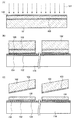
次に、本発明に係るSOI基板の製造方法について説明する。ここでは、図2(A)に示すSOI基板の製造方法の例について、図4乃至図6を用いて説明する。 Next, a method for manufacturing an SOI substrate according to the present invention will be described. Here, an example of a method for manufacturing the SOI substrate illustrated in FIG. 2A will be described with reference to FIGS.
まず、半導体基板101を準備する(図4(A)、図6(A)参照)。半導体基板101としては、市販の半導体基板、例えば、単結晶半導体基板や多結晶半導体基板を用いればよい。具体的には、シリコン基板やゲルマニウム基板などの半導体基板、ガリウムヒ素やインジウムリンなどの化合物半導体基板が挙げられる。市販のシリコン基板としては、直径5インチ(125mm)、直径6インチ(150mm)、直径8インチ(200mm)、直径12インチ(300mm)サイズのものが代表的であり、その形状は円形のものがほとんどである。また、膜厚は1.5mm程度まで適宜選択できる。
First, the
次に、半導体基板101の表面から電界で加速されたイオン104を注入し、所定の深さの領域にイオンドーピング層103を形成する(図4(A)、図6(A)参照)。なお、本明細書におけるイオンの注入は、加速されたイオンを照射して、該照射したイオンを構成する元素を半導体基板中に含ませることを指す。また、イオンドーピング層とは、半導体基板へイオンを照射し、イオンの照射により微小な空洞を有するように脆弱化された領域であり、以下、「イオンドーピング層」を「分離層」という。後の熱処理によって分離層で分断することで、ベース基板上にSOI層を形成することができる。イオン104の照射は、後にベース基板に転置するSOI層の膜厚を考慮して行われる。好ましくは、SOI層の膜厚が5nm乃至500nm、より好ましくは10nm乃至200nmの厚さとなるようにする。イオンを照射する際の加速電圧及びイオンのドーズ量は、転置するSOI層の膜厚を考慮して適宜選択する。イオン104は、水素、ヘリウム、又はフッ素等のハロゲンのイオンを用いることができる。なお、イオン104としては、水素、ヘリウム、又はハロゲン元素から選ばれたソースガスをプラズマ励起して生成された一の原子又は複数の同一の原子からなるイオン種を照射することが好ましい。水素を注入する場合には、H+、H2 +、H3 +イオンを含ませると共に、H3 +イオンの割合を高めておくとイオンの照射効率を高めることができ、照射時間を短縮することができるため好ましい。また、このような構成とすることで、剥離を容易に行うことができる。
Next,
なお、所定の深さに分離層103を形成するために、イオン104を高ドーズ条件で照射する必要がある場合がある。このとき、条件によっては半導体基板101の表面が粗くなってしまう。そのため、半導体基板のイオンが照射される表面に、保護層として窒化シリコン層又は窒化酸化シリコン層などを膜厚50nm乃至200nmの範囲で設けておいてもよい。
Note that in order to form the
次に、半導体基板101に接合層122を形成する(図4(B)、図6(B)参照)。接合層122は、半導体基板101がベース基板と接合を形成する面に形成する。ここで形成する接合層122としては、上述のように有機シランを原料ガスに用いた化学気相成長法により成膜される酸化シリコン層が好ましい。その他に、シランを原料ガスに用いた化学気相成長法により成膜される酸化シリコン層を適用することもできる。化学気相成長法による成膜では、半導体基板101に形成した分離層103から脱ガスが起こらない程度の温度が適用される。例えば、350℃以下の成膜温度が適用される。なお、単結晶半導体基板または多結晶半導体基板などの半導体基板からSOI層を剥離する加熱処理は、化学気相成長法による成膜温度よりも高い加熱処理温度が適用される。
Next, the
次に、半導体基板101を所望の大きさ、形状に加工する(図4(C)、図6(C)参照)。具体的には、所望のパネルサイズとなるように加工する。図6(C)では、円形の半導体基板101を分断して、矩形の半導体基板102を形成する例を示している。この際、接合層122及び分離層103も分断される。つまり、所望のパネルサイズであり、所定の深さに分離層103が形成され、表面(ベース基板との接合面)に接合層122が形成された半導体基板102が得られる。
Next, the
半導体基板102は、各種表示装置のパネルサイズとすることが好ましい。パネルサイズは組み込まれる最終製品等によって適宜選択すればよいが、例えば対角10インチ未満の中小型パネルのパネルサイズとすることができる。例えば、画面サイズ対角2.4インチの携帯電話機に適用する場合、画面サイズ対角2.4インチに画面額縁サイズを考慮したパネルサイズとする。また、半導体基板102の形状も最終製品等、用途によって適宜選択すればよいが、ディスプレイ等の表示装置に適用する場合、アスペクト比3:4程度の矩形とすることが好ましい。また、半導体基板102を矩形状にすると、後の製造工程における加工が容易になり、さらに半導体基板101から効率的に切り出すことも可能になるため好ましい。半導体基板101の分断は、ダイサー或いはワイヤソー等の切断装置、レーザ切断、プラズマ切断、電子ビーム切断、その他任意の切断手段を用いることができる。
The
なお、半導体基板表面に接合層を形成するまでの工程順序は、適宜入れ替えることが可能である。図4及び図6では半導体基板に分離層を形成し、前記半導体基板の表面に接合層を形成した後、前記半導体基板を所望のパネルサイズに加工する例を示している。これに対し、例えば、半導体基板を所望のパネルサイズに加工した後、前記所望のパネルサイズの半導体基板に分離層を形成し、前記所望のパネルサイズの半導体基板の表面に接合層を形成することもできる。 Note that the order of steps until the bonding layer is formed on the surface of the semiconductor substrate can be changed as appropriate. 4 and 6 show an example in which a separation layer is formed on a semiconductor substrate, a bonding layer is formed on the surface of the semiconductor substrate, and then the semiconductor substrate is processed into a desired panel size. On the other hand, for example, after a semiconductor substrate is processed into a desired panel size, a separation layer is formed on the semiconductor substrate having the desired panel size, and a bonding layer is formed on the surface of the semiconductor substrate having the desired panel size. You can also.
次に、ベース基板110と半導体基板102を貼り合わせる。図5(A)には、ベース基板110と半導体基板102の接合層122が形成された面とを密着させ、ベース基板110と接合層122を接合させて、ベース基板110と半導体基板102を貼り合わせる例を示す。なお、接合を形成する面(接合面)は十分に清浄化しておくことが好ましい。ベース基板110と接合層122を密着させることにより接合が形成される。この接合はファンデルワールス力が作用しており、ベース基板110と半導体基板102とを圧接することで、水素結合による強固な接合を形成することが可能である。
Next, the
また、ベース基板110と接合層122との良好な接合を形成するために、接合面を活性化しておいてもよい。例えば、接合を形成する面の一方又は双方に原子ビーム若しくはイオンビームを照射する。原子ビーム若しくはイオンビームを利用する場合には、アルゴン等の不活性ガス中性原子ビーム若しくは不活性ガスイオンビームを用いることができる。その他に、プラズマ照射若しくはラジカル処理を行うことで接合面を活性化することもできる。このような表面処理により、400℃以下の温度であっても異種材料間の接合を形成することが容易となる。
Further, in order to form a favorable bond between the
また、接合層122を介してベース基板110と半導体基板102を貼り合わせた後は、加熱処理又は加圧処理を行うことが好ましい。加熱処理又は加圧処理を行うことで接合強度を向上させることが可能となる。加熱処理の温度は、ベース基板110の耐熱温度以下であることが好ましい。加圧処理においては、接合面に垂直な方向に圧力が加わるように行い、ベース基板110及び半導体基板102の耐圧性を考慮して行う。
In addition, after the
次に、加熱処理を行い、分離層103を劈開面として半導体基板102の一部をベース基板110から剥離する(図5(B)参照)。加熱処理の温度は接合層122の成膜温度以上、ベース基板110の耐熱温度以下で行うことが好ましい。例えば、400℃乃至600℃の加熱処理を行うことにより、分離層103に形成された微小な空洞の体積変化が起こり、分離層103に沿って劈開することが可能となる。接合層122はベース基板110と接合しているので、ベース基板110上には半導体基板102と同じ結晶性のSOI層130が残存することとなる。なお、本明細書における劈開とは、水素、ヘリウム、又はフッ素等のハロゲンのイオンを照射することで微小な空洞を有するように脆弱化された分離層で、半導体基板の一部を剥離してベース基板上にSOI層を形成することを指す。また、劈開面とは、剥離によりベース基板上に設けられたSOI層の分離面(ベース基板と逆側の面)を指す。
Next, heat treatment is performed, and part of the
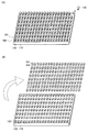
以上で、ベース基板110上に接合層122を介してSOI層130が設けられたSOI構造が形成される。なお、本発明に係るSOI基板は、1枚のベース基板上に接合層を介して複数のSOI層が設けられた構造であることを特徴の1つとする。例えば、分離層が形成され、且つ表面に接合層が形成され、所望のパネルサイズに加工された半導体基板102を、所望の個数準備する。そして、図8(A)に示すようにベース基板110に半導体基板102を所望の個数貼り合わせた後、図8(B)に示すように加熱処理により一括で剥離を行うことで、SOI基板を製造することができる。なお、加熱処理による剥離を一括に行わず、1つ又はある程度の個数の半導体基板102を貼り合わせ、剥離する工程を繰り返して、SOI基板を製造することもできる。
Thus, an SOI structure in which the
また、半導体基板102は、ベース基板110に規則的に配列させると、後の工程が容易になり好ましい。例えば、CCDカメラやコンピュータ等の制御装置を用いることで、規則的に半導体基板102を配列させて貼り合わせていくことが可能になる。また、ベース基板110や半導体基板102にマーカ等を形成して、位置合わせを行ってもよい。なお、図8では隣接するSOI層間はある程度隙間を空けるような構成としているが、極力隙間を空けないように敷き詰めて設ける構成としてもよい。
In addition, it is preferable that the
なお、剥離により得られるSOI層は、その表面を平坦化するため、化学的機械的研磨(Chemical Mechanical Polishing:CMP)を行うことが好ましい。また、CMP等の物理的研磨手段を用いず、SOI層の表面にレーザビームを照射して平坦化を行ってもよい。なお、レーザビームを照射する際は、酸素濃度が10ppm以下の窒素雰囲気下で行うことが好ましい。これは、酸素雰囲気下でレーザビームの照射を行うとSOI層表面が荒れる恐れがあるからである。また、得られたSOI層の薄膜化を目的として、CMP等を行ってもよい。 Note that the SOI layer obtained by peeling is preferably subjected to chemical mechanical polishing (CMP) in order to planarize the surface. Further, planarization may be performed by irradiating the surface of the SOI layer with a laser beam without using physical polishing means such as CMP. Note that the laser beam irradiation is preferably performed in a nitrogen atmosphere with an oxygen concentration of 10 ppm or less. This is because the surface of the SOI layer may be roughened when laser beam irradiation is performed in an oxygen atmosphere. Further, CMP or the like may be performed for the purpose of thinning the obtained SOI layer.
また、図7にベース基板側に接合層を設けてSOI層を形成する工程を示す。ここでは、図3(B)に示すSOI基板の製造方法の例を説明する。 FIG. 7 shows a step of forming an SOI layer by providing a bonding layer on the base substrate side. Here, an example of a method for manufacturing the SOI substrate illustrated in FIG. 3B will be described.
図7(A)は酸化シリコン層126が形成された半導体基板101に電界で加速されたイオン104を照射し、所定の深さに分離層103を形成する工程を示している。酸化シリコン層126は、CVD法やスパッタリング法を用いて形成することもできるが、好ましくは熱酸化法により形成する。また、酸化シリコン層126として、オゾン含有水等で半導体基板表面を処理することにより形成されるケミカルオキサイドを適用してもよい。半導体基板101は、上述の図4(A)の場合と同様のものを適用できる。また、水素、ヘリウム又はフッ素等のハロゲンのイオンの照射も、上述の図4(A)の場合と同様である。半導体基板101の表面に酸化シリコン層126を形成しておくことで、イオンの照射の際に半導体基板表面がダメージを受け、平坦性が損なわれるのを防ぐことができる。
FIG. 7A shows a step of irradiating the
図7(B)は、バリア層152及び接合層154が形成されたベース基板110と、半導体基板102の酸化シリコン層126が形成された面を密着させて接合を形成する工程を示している。ベース基板110上の接合層154と半導体基板102の酸化シリコン層126を密着させることによって接合が形成される。なお、半導体基板102は、分離層103が形成され、表面に酸化シリコン層126が形成された半導体基板101を所望のパネルサイズに加工したものである。バリア層152は、CVD法やスパッタリング法により、酸化シリコン層、窒化シリコン層、酸化窒化シリコン層又は窒化酸化シリコン層を用いて単層構造又は積層構造で形成すればよい。接合層154は、上述の接合層122と同様の酸化シリコン層を形成すればよい。
FIG. 7B illustrates a step of forming a bond by bringing the
そして、図7(C)に示すように半導体基板102の一部を剥離する。剥離のための加熱処理は図5(B)の場合と同様に行い、分離層103を劈開面としてベース基板110から剥離する。剥離処理後、ベース基板110上に半導体基板102と同じ結晶性のSOI層130が残存し、図1(B)に示すようなSOI基板を得ることができる。図7に示すSOI基板は、ベース基板110上にバリア層152、接合層154、酸化シリコン層126を介してSOI層130が設けられた構造を有する。なお、剥離処理後、得られたSOI層を平坦化又は薄膜化するため、CMPやレーザビームの照射等を行ってもよい。
Then, as shown in FIG. 7C, part of the
本発明に係るSOI基板の製造方法は、ガラス基板等の耐熱温度が600℃以下のベース基板110であっても接合部の接着力が強固なSOI層130を得ることができる。また、600℃以下の温度プロセスを適用すればよいため、ベース基板110として、アルミノシリケートガラス、アルミノホウケイ酸ガラス、バリウムホウケイ酸ガラスの如き無アルカリガラスと呼ばれる電子工業用に使われる各種ガラス基板を適用することが可能となる。もちろん、セラミック基板、サファイヤ基板、石英基板等を適用することも可能である。すなわち、一辺が1メートルを超える基板上に単結晶半導体層を形成することができる。このような大面積基板を使って液晶ディスプレイのような表示装置や、半導体集積回路を製造することができる。
With the method for manufacturing an SOI substrate according to the present invention, an
また、本発明に係るSOI基板は、ベース基板上にパネルサイズのSOI層を設ける構成である。このようにすることで、1つのSOI層で所望の表示パネルを形成することができ、歩留まりの向上を図ることができる。また、1つのSOI層で所望の表示パネルを形成することができるため、表示パネルを形成する素子のばらつきを抑制することが可能である。 The SOI substrate according to the present invention has a structure in which a panel-sized SOI layer is provided over a base substrate. In this manner, a desired display panel can be formed using one SOI layer, and yield can be improved. In addition, since a desired display panel can be formed using one SOI layer, variation in elements forming the display panel can be suppressed.
さらに、ベース基板にSOI層を転置して形成する際にSOI層の結晶に欠陥が生じても、パネル毎に歩留まりを管理することができる。また、ベース基板へのSOI層の転置をパネルサイズで行うため、異種材料を貼り合わせる場合も応力等のストレスが緩和でき、歩留まりの向上を図ることができる。 Furthermore, even if a defect occurs in the crystal of the SOI layer when the SOI layer is transferred to the base substrate, the yield can be managed for each panel. In addition, since the SOI layer is transferred to the base substrate in a panel size, stress such as stress can be reduced even when different materials are bonded to each other, and the yield can be improved.
また、本発明に係るSOI基板は、ベース基板上に複数のSOI層を設けることで大面積化を実現できる。よって、一度の製造プロセスで多数の表示パネルを製造することが可能となり、当該表示パネルを組み込んで製造する最終製品の生産性を向上させることができる。 Further, the SOI substrate according to the present invention can realize a large area by providing a plurality of SOI layers on a base substrate. Therefore, a large number of display panels can be manufactured in a single manufacturing process, and productivity of a final product manufactured by incorporating the display panel can be improved.
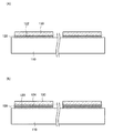
以上のように製造したSOI基板を用いて表示装置を製造することができる。例えば、図9に本発明に係る表示装置の一例の模式図を示す。ここでは、液晶表示装置を形成する一例を示す。図9(A)は上面の模式図の一例を示し、図9(B)は図9(A)の線分OPにおける断面図の一例を示し、図9(C)は表示装置の斜視図の一例を示す。 A display device can be manufactured using the SOI substrate manufactured as described above. For example, FIG. 9 shows a schematic diagram of an example of a display device according to the present invention. Here, an example of forming a liquid crystal display device is shown. FIG. 9A illustrates an example of a schematic top view, FIG. 9B illustrates an example of a cross-sectional view taken along the line OP in FIG. 9A, and FIG. 9C illustrates a perspective view of the display device. An example is shown.
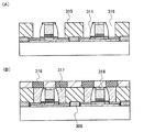
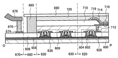
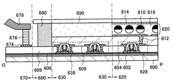
本実施の形態に係る液晶表示装置は、第1の基板600上に設けられた表示部620と、第1の駆動回路部630と、第2の駆動回路部650と、を有する。表示部620、第1の駆動回路部630及び第2の駆動回路部650は、シール材680によって、第1の基板600と第2の基板690との間に封止されている。また、第1の基板600上には、第1の駆動回路部630及び第2の駆動回路部650に外部からの信号や電位を伝達する外部入力端子が接続される端子領域670が設けられる。
The liquid crystal display device according to this embodiment includes a
図9(B)に示すように、表示部620にはトランジスタを有する画素回路部628が設けられている。また、第1の駆動回路部630にはトランジスタを有する周辺回路部638が設けられている。第1の基板600と、画素回路部628及び周辺回路部638との間には、下地絶縁層として機能する絶縁層602、絶縁層604、接合層606が順次積層されている。画素回路部628及び周辺回路部638、或いはその上層には層間絶縁層として機能する絶縁層608、絶縁層609が設けられている。画素回路部628に形成されたトランジスタのソース電極又はドレイン電極は、絶縁層609に形成された開口を介して、画素電極660と電気的に接続される。なお、画素回路部628はトランジスタを用いた回路が集積されているが、ここでは便宜上1つのトランジスタの断面図を示している。同様に、周辺回路部638にもトランジスタを用いた回路が集積されているが、便宜上2つのトランジスタの断面図を示している。
As shown in FIG. 9B, the
画素回路部628及び周辺回路部638上には、画素電極660を覆うように形成された配向膜682と、配向膜687とで挟持された液晶層684が設けられている。液晶層684は、スペーサ686により距離(セルギャップ)が制御されている。配向膜687上には、対向電極688、カラーフィルター689を介して第2基板690が設けられている。第1の基板600及び第2の基板690はシール材680によって固着されている。
Over the
また、第2の基板690の外側には、偏光板692が配設されている。なお、本実施の形態では反射型の液晶表示装置を示すため、第2の基板690に偏光板を設ける例を示す。例えば透過型の液晶表示装置とする場合は、第1の基板600及び第2の基板690の双方に偏光板を設ければよい。
In addition, a
また、端子領域670には、端子電極674が設けられている。該端子電極674は、異方性導電層676によって、外部入力端子678と電気的に接続されている。
A
次に、図9で示した液晶表示装置の製造方法の一例に関して説明する。 Next, an example of a manufacturing method of the liquid crystal display device shown in FIG. 9 will be described.
まず、本発明に係るSOI基板を準備する(図11(A)参照)。ここでは、図2(A)に示すものと類似したSOI基板を適用する例を示す。 First, an SOI substrate according to the present invention is prepared (see FIG. 11A). Here, an example in which an SOI substrate similar to that shown in FIG.
ベース基板である基板600上には、絶縁層602、絶縁層604及び接合層606を介して複数のSOI層610が設けられている。SOI層610は所望のパネルサイズに加工されている。ここでは、便宜的に1つのSOI層を含むパネル形成領域610bを用いて表示装置を製造する例を説明するが、隣接するパネル形成領域610aにも同時に表示装置を製造することが可能である。
A plurality of SOI layers 610 are provided over the
基板600は、絶縁表面を有する基板または絶縁基板を用いる。例えば、アルミノシリケートガラス、アルミノホウケイ酸ガラス、バリウムホウケイ酸ガラスのような電子工業用に使われる各種ガラス基板、石英基板、セラミック基板、サファイヤ基板等を用いる。ここでは、ガラス基板を用いるものとする。
As the
絶縁層602、絶縁層604は、ガラス基板からアルカリ金属若しくはアルカリ土類金属などの可動イオンの拡散を防ぐために設ける。具体的には、上述のバリア層と同様の絶縁層を設ければよい。なお、絶縁層602及び絶縁層604の少なくとも一層は、窒化シリコン層又は窒化酸化シリコン層のなどの窒素を含有する絶縁層を設けることが好ましい。また、接合層606は、上述の接合層122と同様の酸化シリコン層を設ければよい。
The insulating
本実施の形態では、基板600上に絶縁層602、絶縁層604を形成し、SOI層を剥離する半導体基板側に接合層606を形成し、基板600及び前記半導体基板を貼り合わせた後、前記半導体基板の一部を剥離してSOI層610を形成する例を示している。具体的には、基板600に形成された絶縁層604と、半導体基板に形成された接合層606とを密着させ、絶縁層604と接合層606とを接合させて、基板600と半導体基板を貼り合わせる。半導体基板には、所定の深さに水素、ヘリウム又はハロゲンのイオンを照射し分離層を形成しておく。そして、加熱処理を行い、半導体基板に形成された分離層を劈開面として前記半導体基板の一部を剥離し、SOI層610を得る。ここでは、半導体基板側に接合層606を形成するため、該接合層606はSOI層610と同程度の大きさとなる。つまり、隣接するパネル形成領域610a及びパネル形成領域610bとの間で、SOI層610と同様に接合層606も分離している。また、絶縁層602、絶縁層604はベース基板である基板600上に形成するため、隣接するパネル形成領域610a及びパネル形成領域610bで連続する層となる。なお、適用するSOI基板は本発明に係るいずれの構造でもよく、上述の図2(A)乃至図3(B)のいずれの構造を適用してもよい。例えば、ベース基板側に接合層を設けてもよいし、半導体基板と接合層との間に熱酸化膜等の絶縁層を設けてもよい。
In this embodiment, the insulating
SOI層610を選択的にエッチングして、表示部620に第1のSOI層621と、第1の駆動回路部630に第2のSOI層631と、第3のSOI層641と、を形成する。そして、第1のSOI層621、第2のSOI層631及び第3のSOI層641上に、ゲート絶縁層612を介してゲート電極614を形成する(図11(B)参照)。
The
第1のSOI層621、第2のSOI層631及び第3のSOI層641は、SOI層610を選択的にエッチングして所望の形状に加工する。ここではSOI層610を複数の島状に加工し、分離させる。準備したSOI基板のSOI層よりも、第1のSOI層621、第2のSOI層631及び第3のSOI層641の膜厚を薄くしたい場合には、該SOI層をエッチングして薄膜化してもよい。また、SOI層の一部を変質させて、該変質した部分を選択的にエッチングして薄膜化してもよい。ここでSOI層の変質とは、例えば酸化処理、窒化処理等を示す。また、第1のSOI層621、第2のSOI層631及び第3のSOI層641は、適宜エッチング条件等を制御して、端部が垂直に近いテーパ形状となるように形成してもよいし、緩やかなテーパ形状となるように形成してもよい。例えば、テーパ角が45°以上95°未満、好ましくは60°以上95°未満となるような形状としてもよいし、テーパ角が45°未満の緩やかな形状としてもよい。
The
なお、完成するトランジスタの閾値電圧を制御するため、第1のSOI層621、第2のSOI層631及び第3のSOI層641に低濃度の一導電型を付与する不純物元素を添加してもよい。この場合、トランジスタのチャネル形成領域にも不純物元素が添加されることになる。なお、ここで添加する不純物元素は、ソース領域又はドレイン領域として機能する高濃度不純物領域及びLDD領域として機能する低濃度不純物領域よりも低い濃度で添加する。
Note that an impurity element imparting one conductivity type at a low concentration may be added to the
ゲート電極614は、基板全面に導電層を形成した後、該導電層を選択的にエッチングして所望の形状に加工する。ここでは、ゲート電極614として導電層の積層構造を形成した後、選択的にエッチングして、分離した導電層が第1のSOI層621、第2のSOI層631及び第3のSOI層641をそれぞれ横断するように加工している。
The
ゲート電極614を形成する導電層は、CVD法やスパッタリング法により、タンタル(Ta)、タングステン(W)、チタン(Ti)、モリブデン(Mo)、クロム(Cr)、アルミニウム(Al)、銅(Cu)、又はニオブ(Nb)等の金属元素、又は当該金属元素を含む合金材料若しくは化合物材料を用いて基板全面に導電層を形成した後、当該導電層を選択的にエッチングして形成することができる。また、リン等の一導電型を付与する不純物元素が添加された多結晶シリコンに代表される半導体材料を用いて形成することもできる。
The conductive layer forming the
なお、ここではゲート電極614を2層の導電層の積層構造で形成する例を図示するが、ゲート電極は単層構造でも3層以上の積層構造でもよい。また、導電層の側面をテーパ形状としてもよい。ゲート電極を導電層の積層構造とする場合、下層の導電層の幅を大きくしてもよいし、各層の側面を異なる角度のテーパ形状としてもよい。
Note that although an example in which the
第1のSOI層621、第2のSOI層631及び第3のSOI層641と、ゲート電極614との間には、ゲート絶縁層612を形成する。ゲート絶縁層612は、CVD法、スパッタリング法、ALD法等を用いて、酸化シリコン、酸化窒化シリコン、酸化ハフニウム、酸化アルミニウム、酸化タンタルなどの材料を用いて形成することができる。また、第1のSOI層621、第2のSOI層631及び第3のSOI層641をプラズマ処理により固相酸化又は固相窒化して形成することもできる。その他、CVD法等により絶縁層を形成した後、当該絶縁層をプラズマ処理により固相酸化又は固相窒化して形成してもよい。
A
固相酸化処理若しくは固相窒化処理は、マイクロ波(代表的には2.45GHz)等の高周波により励起されたプラズマを用いて行うことが好ましい。具体的には、高周波を用いて励起された電子密度が1×1011cm−3以上1×1013cm−3以下、且つ電子温度が0.5eV以上1.5eV以下のプラズマを利用してプラズマ処理を行うことが好ましい。これは、固相酸化処理若しくは固相窒化処理において、500℃以下の温度において、緻密な絶縁層を形成すると共に実用的な反応速度を得るためである。
The solid-phase oxidation treatment or solid-phase nitridation treatment is preferably performed using plasma excited by a high frequency such as a microwave (typically 2.45 GHz). Specifically, an electron density excited using high frequency is 1 × 10 11
プラズマ処理により第1のSOI層621、第2のSOI層631及び第3のSOI層641の表面を酸化する場合には、酸素を含む雰囲気下(例えば、酸素、オゾン、亜酸化窒素、一酸化窒素若しくは二酸化窒素、及び希ガス(ヘリウム(He)、ネオン(Ne)、アルゴン(Ar)、クリプトン(Kr)、キセノン(Xe)の少なくとも1つを含む)を含む雰囲気下、又は酸素、オゾン、亜酸化窒素、一酸化窒素若しくは二酸化窒素と、水素と、希ガスとを含む雰囲気下)で行う。また、プラズマ処理により第1のSOI層621、第2のSOI層631及び第3のSOI層641上に形成された絶縁層の表面を窒化する場合には、窒素を含む雰囲気下(例えば、窒素と希ガス(He、Ne、Ar、Kr、Xeの少なくとも一つを含む)を含む雰囲気下、窒素と水素と希ガスを含む雰囲気下、又はNH3と希ガスを含む雰囲気下)でプラズマ処理を行う。希ガスとしては、例えばArを用いることが好ましい。また、ArとKrを混合したガスを用いてもよい。
In the case where the surfaces of the
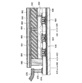
ここで、プラズマ処理を行うためのプラズマ処理装置1080の構成例を図16に示す。当該プラズマ処理装置1080は、支持台1088と、ガスを供給するためのガス供給部1084、ガスを排気するために真空ポンプに接続する排気口1086、アンテナ1098、誘電体板1082、プラズマ発生用の高周波を入力する高周波供給部1092を有している。被処理体1010は、支持台1088によって保持される。また、支持台1088に温度制御部1090を設けることによって、被処理体1010の温度を制御することも可能である。被処理体1010は、プラズマ処理をする基体であり、本実施の形態では基板600上に絶縁層602、絶縁層604、接合層606、第1のSOI層621、第2のSOI層631及び第3のSOI層641が積層形成されたものに相当する。或いは、第1のSOI層621、第2のSOI層631及び第3のSOI層641上に絶縁層が形成されたものに相当する。
Here, FIG. 16 shows a configuration example of a
以下、図16に示すプラズマ処理装置1080を用いてSOI層表面に絶縁層を形成する具体例を述べる。なお、プラズマ処理とは、基板、半導体層(SOI層)、絶縁層、導電層に対する酸化処理、窒化処理、酸化窒化処理、及び水素化処理などの表面改質処理を範疇に含んでいる。これらの処理は、その目的に応じて、ガス供給部1084から供給するガスを選択すれば良い。
Hereinafter, a specific example in which an insulating layer is formed on the surface of the SOI layer using the
まず、図16に示すプラズマ処理装置1080の処理室内を真空にする。そして、ガス供給部1084から希ガス、酸素又は窒素を含むガスを供給する。被処理体1010は室温、若しくは温度制御部1090により100℃以上550℃以下の範囲で加熱する。被処理体1010と誘電体板1082との間隔(以下、電極間隔ともいう)は、20mm以上200mm以下(好ましくは20mm以上60mm以下)程度である。
First, the processing chamber of the
次に、高周波供給部1092からアンテナ1098に高周波を入力する。ここでは、高周波としてマイクロ波(周波数2.45GHz)を入力する。そしてマイクロ波をアンテナ1098から誘電体板1082を通して処理室内に入力することによって、プラズマ1094を生成し、当該プラズマ1094によって酸素ラジカル(OHラジカルを含む場合もある)又は窒素ラジカル(NHラジカルを含む場合もある)を生成する。このとき、プラズマ1094は、供給されたガスによって生成される。
Next, a high frequency is input from the high
マイクロ波等の高周波の入力によりプラズマ1094を生成すると、低電子温度(3eV以下、好ましくは1.5eV以下)で高電子密度(1×1011cm−3以上)のプラズマを生成することができる。具体的には、電子温度が0.5eV以上1.5eV以下、且つ電子密度が1×1011cm−3以上1×1013cm以下のプラズマ生成することが好ましい。なお、本明細書では、マイクロ波の入力により生成された低電子温度で高電子密度のプラズマを高密度プラズマともいう。また、高密度プラズマを利用してプラズマ処理を行うことを高密度プラズマ処理ともいう。
When the
プラズマ1094により生成された酸素ラジカル(OHラジカルを含む場合もある)又は窒素ラジカル(NHラジカルを含む場合もある)によって、被処理体1010に形成されたSOI層の表面が酸化されて絶縁層が形成される。或いは、SOI層上に形成された絶縁層の表面又は表面近傍が酸化又は窒化される。このとき、供給するガスにアルゴンなどの希ガスを混合させると、希ガスの励起種により酸素ラジカルや窒素ラジカルを効率良く生成することができる。なお、供給ガスに希ガスを用いる場合、形成された絶縁層に希ガスが含まれる場合がある。この方法は、プラズマで励起した活性なラジカルを有効に使うことにより、500℃以下の低温で固相反応による酸化、窒化を行うことができる。
The surface of the SOI layer formed on the object to be processed 1010 is oxidized by oxygen radicals (which may include OH radicals) or nitrogen radicals (which may include NH radicals) generated by the
本実施の形態において、ゲート絶縁層612をプラズマ処理により形成する好適な作製方法の一例は、酸素を含む雰囲気下で第1のSOI層621、第2のSOI層631及び第3のSOI層641をプラズマ処理して酸化シリコン層を形成した後、窒素を含む雰囲気下で酸化シリコン層の表面を窒化プラズマ処理して窒素プラズマ処理層を形成する。具体的には、まず酸素を含む雰囲気下でプラズマ処理を行い、第1のSOI層621、第2のSOI層631及び第3のSOI層641上に3nm乃至6nmの厚さで酸化シリコン層を形成する。続けて、窒素を含む雰囲気下でプラズマ処理を行い、酸化シリコン層の表面又は表面近傍に窒素濃度の高い窒素プラズマ処理層を形成する。なお、表面近傍とは、酸化シリコン層の表面から概略0.25nm乃至1.5nmの深さをいう。例えば、酸化シリコン層を形成した後、窒素を含む雰囲気下でプラズマ処理を行うことによって、酸化シリコン層の表面から概略1nmの深さに窒素を20原子%乃至50原子%の割合で含有した窒素プラズマ処理層を形成することができる。窒素プラズマ処理層は、プラズマ処理の条件によって、窒化シリコン又は窒化酸化シリコンで形成される。
In this embodiment, an example of a preferable manufacturing method for forming the
いずれにしても、上記のようなプラズマ処理による固相酸化処理若しくは固相窒化処理を用いることで、基板600として耐熱温度が600℃以下のガラス基板を用いても、950℃乃至1050℃の範囲で形成される熱酸化膜と同等な絶縁層を得ることができる。すなわち、半導体素子、特にトランジスタや不揮発性記憶素子のゲート絶縁層として機能する絶縁層として信頼性の高い絶縁層を形成することができる。
In any case, by using the solid-phase oxidation treatment or solid-phase nitridation treatment by the plasma treatment as described above, even if a glass substrate having a heat resistant temperature of 600 ° C. or less is used as the
なお、図11(B)では、ゲート絶縁層612とゲート電極614の側端部が揃うように加工される例を示すが、特に限定されず、ゲート電極614のエッチングにおいてゲート絶縁層612を残すように加工してもよい。
Note that FIG. 11B illustrates an example in which the side end portions of the
また、ゲート絶縁層612に高誘電率物質(high−k材料といわれる)を用いる場合には、ゲート電極614を多結晶シリコン、シリサイド、金属若しくは金属窒化物で形成する。好ましくは金属若しくは金属窒化物で形成することが望ましい。例えば、ゲート電極614のうちゲート絶縁層612と接する導電層を金属窒化物材料で形成し、その上の導電層を金属材料で形成する。この組み合わせを用いることによって、ゲート絶縁層を薄膜化した場合でもゲート電極に空乏層が広がってしまうことを防止でき、微細化した場合にもトランジスタの駆動能力を損なうことを防止できる。
In the case where a high dielectric constant material (referred to as a high-k material) is used for the
次に、ゲート電極614上に絶縁層616を形成する。そして、ゲート電極614をマスクとして一導電型を付与する不純物元素を添加する(図11(C)参照)。ここでは、第1の駆動回路部630に形成された第2のSOI層631及び第3のSOI層641に相異なる導電型を付与する不純物元素を添加する例を示す。また、表示部620に形成された第1のSOI層621には第2のSOI層631と同じ導電型を付与する不純物元素を添加する例を示す。
Next, an insulating
表示部620に形成された第1のSOI層621には、ゲート電極614をマスクとして自己整合的に一対の不純物領域623と、当該一対の不純物領域623の間に位置するチャネル形成領域622が形成される。
In the
第1の駆動回路部630に形成された第2のSOI層631には、ゲート電極614をマスクとして自己整合的に一対の不純物領域633と、当該一対の不純物領域633の間に位置するチャネル形成領域632が形成される。第3のSOI層641には、ゲート電極614をマスクとして自己整合的に一対の不純物領域643と、当該一対の不純物領域643の間に位置するチャネル形成領域642が形成される。不純物領域633及び不純物領域643は、相異なる導電型の不純物元素が添加されている。
In the
一導電型を付与する不純物元素としては、ボロン(B)、アルミニウム(Al)、ガリウム(Ga)等のp型を付与する元素、リン(P)、ヒ素(As)等のn型を付与する元素を用いることができる。本実施の形態では、表示部620に形成された第1のSOI層621、第1の駆動回路部630に形成された第2のSOI層631にn型を付与する元素、例えばリンを添加する。また、第3のSOI層641にp型を付与する元素、例えばボロンを添加する。なお、第1のSOI層621、第2のSOI層631に不純物元素を添加する際は、レジストマスク等を用いて第3のSOI層641を選択的に覆えばよい。同様に、第3のSOI層641に不純物元素を添加する際は、レジストマスク等を用いて第1のSOI層621、第2のSOI層631を選択的に覆えばよい。
As an impurity element imparting one conductivity type, an element imparting p-type such as boron (B), aluminum (Al), or gallium (Ga), or n-type such as phosphorus (P) or arsenic (As) is imparted. Elements can be used. In this embodiment mode, an element imparting n-type conductivity, for example, phosphorus is added to the
絶縁層616は、CVD法、スパッタリング法、ALD法等を用いて、酸化シリコン或いは酸化窒化シリコン、又は窒化シリコン或いは窒化酸化シリコンなどの材料を用いて形成することができる。一導電型を付与する不純物元素を添加する際に、絶縁層616を通過させて添加する構成とすることで、SOI層に与えるダメージを低減することができる。
The insulating
次に、ゲート電極614の側面にサイドウォール絶縁層618を形成する。そして、ゲート電極614及びサイドウォール絶縁層618をマスクとして一導電型を付与する不純物元素を添加する(図11(D)参照)。なお、第1のSOI層621、第2のSOI層631及び第3のSOI層641には、それぞれ先の工程(不純物領域623、不純物領域633及び不純物領域643を形成する工程)で添加した不純物元素と同じ導電型の不純物元素を添加する。また、先の工程で添加した不純物元素よりも高い濃度で添加する。
Next, a
第1のSOI層621には、ゲート電極614及びサイドウォール絶縁層618をマスクとして自己整合的に一対の高濃度不純物領域626と、一対の低濃度不純物領域624が形成される。ここで形成される高濃度不純物領域626はソース領域又はドレイン領域として機能し、低濃度不純物領域624はLDD(Lightly Doped Drain)領域として機能する。
In the
第2のSOI層631には、ゲート電極614及びサイドウォール絶縁層618をマスクとして自己整合的に一対の高濃度不純物領域636と、一対の低濃度不純物領域634が形成される。ここで形成される高濃度不純物領域636はソース領域又はドレイン領域として機能し、低濃度不純物領域634はLDD領域として機能する。第3のSOI層641には、ゲート電極614及びサイドウォール絶縁層618をマスクとして自己整合的に一対の高濃度不純物領域646と、一対の低濃度不純物領域644が形成される。なお、第1のSOI層621、第2のSOI層631に不純物元素を添加する際は、レジストマスク等を用いて第3のSOI層641を選択的に覆えばよい。同様に、第3のSOI層641に不純物元素を添加する際は、レジストマスク等を用いて第1のSOI層621、第2のSOI層631を選択的に覆えばよい。
In the
サイドウォール絶縁層618は、絶縁層616を介してゲート電極614の側面に設けられる。例えば、ゲート電極614を埋め込むように形成した絶縁層を、垂直方向を主体とした異方性エッチングを行うことによって、ゲート電極614の側面に自己整合的に形成することができる。サイドウォール絶縁層618は、窒化シリコン或いは窒化酸化シリコン、又は酸化シリコン或いは酸化窒化シリコンなどの材料を用いて形成することができる。なお、絶縁層616を酸化シリコン又は酸化窒化シリコンを用いて形成する場合、サイドウォール絶縁層618を窒化シリコン又は窒化酸化シリコンを用いて形成することで、絶縁層616をエッチングストッパーとして機能させることができる。また、絶縁層616を窒化シリコン又は窒化酸化シリコンを用いて形成する場合は、サイドウォール絶縁層618を酸化シリコン又は酸化窒化シリコンを用いて形成すればよい。このように、エッチングストッパーとして機能しうる絶縁層を設けることで、サイドウォール絶縁層を形成する際のオーバーエッチングによりSOI層がエッチングされてしまうのを防ぐことができる。
The
次に、絶縁層616の露出部をエッチングする(図12(A)参照)。絶縁層616は、サイドウォール絶縁層618及びゲート電極614の間、サイドウォール絶縁層618及び第1のSOI層621の間、サイドウォール絶縁層618及び第2のSOI層631の間、並びにサイドウォール絶縁層618及び第3のSOI層641の間に残る。
Next, the exposed portion of the insulating
なお、ソース領域又はドレイン領域として機能する高濃度不純物領域を低抵抗化するため、シリサイド層を形成してもよい。シリサイド層としては、コバルトシリサイド若しくはニッケルシリサイドを適用すれば良い。SOI層の膜厚が薄い場合には、高濃度不純物領域が形成されたSOI層の底部までシリサイド反応を進めてフルシリサイド化しても良い。 Note that a silicide layer may be formed in order to reduce resistance of the high-concentration impurity region functioning as a source region or a drain region. As the silicide layer, cobalt silicide or nickel silicide may be applied. When the thickness of the SOI layer is small, the silicide reaction may be advanced to the bottom of the SOI layer in which the high concentration impurity region is formed to form a full silicide.
次に、基板600全面に絶縁層608を形成した後、該絶縁層608を選択的にエッチングして、表示部620の第1のSOI層621に形成された高濃度不純物領域626に達する開口を形成する。また、第1の駆動回路部630の第2のSOI層631、第3のSOI層641に形成された高濃度不純物領域636、高濃度不純物領域646にそれぞれ達する開口を形成する。そして、該開口を埋め込むように導電層619を形成する。また、端子領域670に端子電極674を形成する(図12(B)参照)。
Next, after an
絶縁層608は、CVD法やスパッタリング法、ALD法、又は塗布法等により、単層構造又は積層構造で形成する。例えば、絶縁層608は、CVD法、スパッタリング法、又はALD法により、酸化シリコン、窒化シリコン、酸化窒化シリコン、窒化酸化シリコン等の酸素若しくは窒素を含む無機絶縁材料や、DLC(ダイヤモンドライクカーボン)等の炭素を含む絶縁材料を用いて形成することもできるし、塗布法により、エポキシ、ポリイミド、ポリアミド、ポリビニルフェノール、ベンゾシクロブテン、アクリル等の有機絶縁材料またはシロキサン樹脂等のシロキサン材料を用いて形成することもできる。また、無機絶縁材料や炭素を含む絶縁材料を用いて形成した層と、有機絶縁材料やシロキサン材料を用いて形成した層の積層構造とすることもできる。なお、シロキサン材料とは、Si−O−Si結合を含む材料に相当する。シロキサンは、シリコン(Si)と酸素(O)との結合で骨格構造が構成される。置換基として、少なくとも水素を含む有機基(例えばアルキル基、芳香族炭化水素)が用いられる。置換基として、フルオロ基を用いることもできる。または置換基として、少なくとも水素を含む有機基と、フルオロ基とを用いてもよい。また、絶縁層608は、CVD法やスパッタリング法、ALD法を用いて絶縁層を形成した後、当該絶縁層に酸素雰囲気下又は窒素雰囲気下でプラズマ処理を行ってもよい。ここでは絶縁層608は単層構造の例を示すが、2層以上の積層構造としてもよい。また、無機絶縁層や、有機絶縁層を組み合わせて形成してもよい。例えば、基板600全面にパッシベーション層として機能できる窒化シリコン膜や窒化酸化シリコン膜を形成し、その上層に平坦化層として機能できるリンシリケートガラス(PSG)やボロンリンシリケートガラス(BPSG)を材料に用いた絶縁層を形成することができる。
The insulating
導電層619は、ソース電極又はドレイン電極として機能する電極として機能する。ソース電極又はドレイン電極として機能する導電層619は、絶縁層608に形成された開口を介して、第1のSOI層621、第2のSOI層631又は第3のSOI層641と電気的に接続される。
The
導電層619は、CVD法やスパッタリング法を用いて、アルミニウム(Al)、タングステン(W)、チタン(Ti)、タンタル(Ta)、モリブデン(Mo)、ニッケル(Ni)、白金(Pt)、銅(Cu)、金(Au)、銀(Ag)、マンガン(Mn)、ネオジム(Nd)、炭素(C)、シリコン(Si)等の金属元素、又は当該金属元素を含む合金材料若しくは化合物材料を用いて基板全面に導電層を単層構造又は積層構造で形成した後、当該導電層を選択的にエッチングして形成することができる。アルミニウムを含む合金材料としては、例えば、アルミニウムを主成分としニッケルを含む材料、又は、アルミニウムを主成分とし、ニッケルと、炭素とシリコンの一方又は両方とを含む合金材料があげられる。また、タングステンを含む化合物材料としては、例えばタングステンシリサイドが挙げられる。導電層619は、例えば、バリア層とアルミニウムシリコン層とバリア層の積層構造、バリア層とアルミニウムシリコン層と窒化チタン層とバリア層の積層構造を採用することができる。なお、バリア層とは、チタン、チタンの窒化物、モリブデン、又はモリブデンの窒化物からなる薄膜に相当する。アルミニウムやアルミニウムシリコンは抵抗値が低く、安価であるため、ソース電極又はドレイン電極として機能する導電層を形成する材料として最適である。また、ソース電極又はドレイン電極として機能する導電層を、上層と下層にバリア層を設けた積層構造とすると、アルミニウムやアルミニウムシリコンのヒロックの発生を防止することができるため好ましい。
The
端子領域670に形成される端子電極674は、後に形成されるFPC等の外部入力端子と第1の駆動回路部630及び第2の駆動回路部650とを電気的に接続させるための電極として機能する。ここでは、導電層619と同一の材料を用いた同一層で端子電極674を形成する例を示している。
The
以上で、表示部620に第1のSOI層621を有するトランジスタが形成された画素回路部628が形成される。また、第1の駆動回路部630に第2のSOI層631を有するトランジスタ及び第3のSOI層641を有するトランジスタが形成された周辺回路部638が形成される。
Through the above steps, the
次に、表示部620及び第1の駆動回路部630上に絶縁層609を形成する。次に、表示部620上に形成された絶縁層609を選択的にエッチングして、画素回路部628に形成されたトランジスタの導電層619に達する開口を形成する。そして、該開口を埋め込むように画素電極660を形成する(図12(C)参照)。
Next, an insulating
絶縁層609は、表示部620及び第1の駆動回路部630の凹凸を平滑化して、平坦な表面を形成できる平坦化層を形成することが好ましい。例えば、エポキシ、ポリイミド、ポリアミド、ポリビニルフェノール、ベンゾシクロブテン、アクリル等の有機絶縁材料またはシロキサン樹脂等のシロキサン材料を用いて形成することができる。ここでは絶縁層609は単層構造の例を示すが、2層以上の積層構造としてもよい。積層構造にする場合、例えば、有機樹脂などを上層にし、酸化シリコン、窒化シリコンまたは酸化窒化シリコン等の無機絶縁層を下層にした積層構造、又は無機絶縁層で有機絶縁層を挟持する構造とすることができる。なお、絶縁層609は基板全面に形成した後、所望の領域(ここでは表示部620及び第1の駆動回路部630)以外を選択的にエッチングして形成することができる。また、絶縁層609は、各種印刷法(スクリーン印刷、平版印刷、凸版印刷、グラビア印刷等)、液滴吐出法、ディスペンサ法等を用いて選択的に形成することもできる。
The insulating
画素電極660は、本実施の形態では反射電極として機能する。よって、反射性のある導電性材料を用いて形成する。このような材料としては、タンタル(Ta)、タングステン(W)、チタン(Ti)、モリブデン(Mo)、アルミニウム(Al)、クロム(Cr)、銀(Ag)等の金属元素、又は当該金属元素を含む合金材料若しくは化合物材料を用いることができる。なお、他に反射層を形成する場合、若しくは透過型液晶表示装置とする場合には、透光性を有する導電材料を用いて画素電極660を形成すればよい。透光性を有する導電性材料としては、インジウム錫酸化物(ITO)、酸化シリコンを含むインジウム錫酸化物(ITSO)、酸化亜鉛(ZnO)、酸化インジウム亜鉛(IZO)、又はガリウムを添加した酸化亜鉛(GZO)等を用いることができる。
The
次に、スペーサ686を形成した後、画素電極660及びスペーサ686を覆うように配向膜682を形成する。次に、表示部620及び第1の駆動回路部630、第2の駆動回路部650を囲うようにシール材680を形成する(図13(A)参照)。
Next, after the
スペーサ686は、エポキシ、ポリイミド、ポリアミド、ポリイミドアミド、アクリル等の有機絶縁材料、若しくは酸化シリコン、窒化シリコン、酸化窒化シリコン、窒化酸化シリコン等の無機絶縁材料を用いて、単層構造又は積層構造で形成することができる。本実施の形態ではスペーサ686として柱状スペーサを形成するため、基板全面に絶縁層を形成した後、エッチング加工して所望の形状のスペーサを得る。なお、スペーサ686の形状は特に限定されず、球状のスペーサを散布してもよい。スペーサ686により、セルギャップを保持することができる。
The
配向膜682は、利用する液晶の動作モードに対応して材料を選択すればよく、液晶を一定方向に配列させることが可能な層を形成する。例えばポリイミド、ポリアミド等の材料を用いて形成し、配向処理を行うことで配向膜として機能させることができる。配向処理としては、ラビングや、紫外線等の光照射などを行えばよい。配向膜682の形成方法は特に限定されないが、各種印刷法や液滴吐出法を用いると、絶縁層609上に選択的に形成することができる。
For the
シール材680は、表示装置完成後、少なくとも表示領域を囲うように形成する。本実施の形態では、表示部620、第1の駆動回路部630及び第2の駆動回路部650の周辺を囲うように枠状のシールパターンを形成する。シール材680としては、熱硬化樹脂や光硬化樹脂を用いることができる。なお、シール材にフィラーを含ませることでセルギャップを保持させることもできる。シール材680は、後に対向電極、カラーフィルター等設けられた基板と封止する際に、光照射、加熱処理等を行って硬化を行う。
The
シール材680に囲まれた領域に液晶層684を形成する。また、カラーフィルター689、対向電極688、配向膜687が順次積層された第2の基板690と第1の基板600を貼り合わせる(図13(B)参照)。
A
液晶層684は、所望の液晶材料を用いて形成する。例えば、液晶層684は、シール材680で形成された枠状のシールパターン内に液晶材料を滴下して形成することができる。液晶材料の滴下は、ディスペンサ法や液滴吐出法を用いて行えばよい。なお、液晶材料は予め減圧下で脱気しておくか、滴下後に減圧下で脱気することが好ましい。また、液晶材料の滴下の際に不純物等混入しないように、不活性雰囲気下で行うことが好ましい。また、液晶材料を滴下して液晶層684を形成した後、第1の基板600及び第2の基板690を貼り合わせるまでは、液晶層684に気泡等入らないように減圧下で行うことが好ましい。
The
また、液晶層684は、第1の基板600と第2の基板690を貼り合わせた後、シール材680の枠状パターン内に、毛細管現象を利用して液晶材料を注入して形成することもできる。この場合、あらかじめシール材等に液晶の注入口となる部分を形成しておく。なお、液晶材料は、減圧下で注入を行うことが好ましい。
Alternatively, the
第1の基板600と第2の基板690は、対向させて密着させた後、シール材680を硬化させて貼り合わせることができる。このとき、第2の基板690に設けられた配向膜687と、第1の基板600に設けられた配向膜682とで、液晶層684が挟持される構造となるように貼り合わせる。なお、第1の基板600と第2の基板690の貼り合わせ及び液晶層684の形成を行った後、加熱処理を行って液晶層684の配向乱れを修正することも可能である。
The
第2の基板690は、透光性を有する基板を用いる。例えば、アルミノシリケートガラス、アルミノホウケイ酸ガラス、バリウムホウケイ酸ガラス等の各種ガラス基板、石英基板、セラミック基板、サファイヤ基板等を用いることができる。
As the
第2の基板690上には、貼り合わせる前に、カラーフィルター689、対向電極688、配向膜687を順に形成しておく。なお、第2の基板690には、カラーフィルター689の他にブラックマトリクスを設けてもよい。また、カラーフィルター689は第2の基板690の外側に設けてもよい。また、モノカラー表示とする場合は、カラーフィルター689を設けなくともよい。また、シール材を第2の基板690側に設けてもよい。なお、シール材を第2の基板690側に設ける場合は、液晶材料は第2の基板690に設けられたシール材の枠状パターン内に滴下する。
On the
対向電極688は、インジウム錫酸化物(ITO)、酸化シリコンを含むインジウム錫酸化物(ITSO)、酸化亜鉛(ZnO)、酸化インジウム亜鉛(IZO)、又はガリウムを添加した酸化亜鉛(GZO)等の透光性を有する導電材料を用いて形成することができる。配向膜687は、上記配向膜682と同様に形成することができる。
The
以上により、第1の基板600と第2の基板690との間に、液晶層684を含む表示部620、第1の駆動回路部630及び第2の駆動回路部650が封止された構造が得られる。なお、表示部620及び第1の駆動回路部630、第2の駆動回路部650に形成される回路部には、トランジスタの他、抵抗や、コンデンサなどを同時に作製してもよい。また、トランジスタの構造は特に限定されない。例えば、1つのSOI層に対して複数のゲートを設けたマルチゲート構造とすることもできる。
Thus, a structure in which the
次に、貼り合わせた第1の基板600及び第2の基板690を分断して、所望のパネルサイズに加工する(図14(A)参照)。ここでは、パネル形成領域610a、パネル形成領域610bが分離するように分断する。分断面では、端子電極674が露出する。なお、液晶層684を含む表示部620や第1の駆動回路部630は、シール材680によって封止されている。第1の基板600及び第2の基板690の分断は、スクライバー装置、ブレイカー装置、ロールカッターなどの切断装置を用いて行うことができる。
Next, the bonded
次に、端子領域670上の第2の基板690を分断する(図14(B)参照)。ここでは、端子電極674上の第2の基板690、カラーフィルター689、対向電極688及び配向膜687を除去するように分断する。以上で、所望のパネルサイズを有する表示パネルを得ることができる。
Next, the
ここで、貼り合わせた基板の分断について、図10に示す上面の模式図を用いて詳しく説明する。 Here, the division of the bonded substrates will be described in detail with reference to a schematic diagram of an upper surface shown in FIG.
図10(A)は、図11(A)に示すSOI基板に相当する上面の模式図を示している。ここでは、一枚の基板600上に、それぞれ分離されたSOI層610を有するパネル形成領域610a、パネル形成領域610b、パネル形成領域610c、パネル形成領域610dが設けられている例を示している。パネル形成領域610a、610b、610c、610dにそれぞれ設けられているSOI層610は、所望のパネルサイズとなっている。
FIG. 10A is a schematic diagram of an upper surface corresponding to the SOI substrate illustrated in FIG. Here, an example is shown in which a
図10(B)は、図11(B)乃至図13(A)に示す工程を経て、図13(B)に示すような第1の基板600及び第2の基板690の貼り合わせの工程まで終了した上面の模式図を示している。それぞれのパネル形成領域610a、610b、610c、610d毎に、表示部620、第1の駆動回路部630、第2の駆動回路部650が設けられシール材680によって封止されている。なお、図13(B)は図10(B)の線分QRの断面図に相当する。
In FIG. 10B, the process shown in FIGS. 11B to 13A is performed and the process of bonding the
次に、貼り合わせた第1の基板600及び第2の基板690を図10(B)の矢印6002、矢印6004に沿って分断し、図10(C)に示すようにパネル形成領域毎に分離する。なお、図14(A)は図10(C)の線分Q’R’の断面図に相当する。
Next, the bonded
次に、第2の基板690を図10(C)の矢印6012、矢印6014に沿って分断し、図10(D)に示すように端子領域670を露出させる。端子領域670には端子電極674が設けられており、後に形成される外部入力端子と異方性導電層等を用いて接続される。なお、図14(B)は図10(D)の線分Q’’R’’の断面図に相当する。以上で、表示パネル6100a、表示パネル6100b、表示パネル6100c、表示パネル6100dを得ることができる。表示パネル6100aを構成する素子は、パネル形成領域610aに設けられた1つのSOI層で形成される。同様に、他の表示パネルを構成する素子も、それぞれのパネル形成領域に設けられた1つのSOI層で形成される。よって、特性のばらつきを抑えることができる。
Next, the
なお、ここでは貼り合わせた第1の基板600及び第2の基板690を分断した後、さらに第2の基板690を分断する例を示したが、予め所望のサイズに加工しておいた第2の基板690を貼り合わせる構成としてもよい。
Note that, here, an example in which the
また、ここでは便宜的に1枚のベース基板から4枚の表示パネルを製造する例を示したが、本発明は特に限定されない。上述したように、本発明に係るSOI基板は所望のパネルサイズのSOI層が複数設けられており、個々のSOI層を用いて同時に複数の表示パネルを製造することが可能である。よって、ベース基板上に設けられたSOI層の数に比例して面取り数も増大するため、生産性が飛躍的に向上する。 Although an example in which four display panels are manufactured from one base substrate is shown here for convenience, the present invention is not particularly limited. As described above, the SOI substrate according to the present invention includes a plurality of SOI layers having a desired panel size, and a plurality of display panels can be manufactured simultaneously using individual SOI layers. Accordingly, the number of chamfers increases in proportion to the number of SOI layers provided on the base substrate, so that productivity is dramatically improved.
次に、第2の基板690に偏光板692を設ける。また、端子電極674に異方性導電層676を介して外部入力端子678を接続し、表示パネルを外部と電気的に接続させる構成とする(図15参照)。
Next, a
偏光板692は、第2の基板690の外側(液晶層684等を封止していない面側)に設ける。なお、透過型の液晶表示装置とする場合は、第1の基板600の外側(液晶層684等を封止していない面側)にも偏光板を設ければよい。また、偏光板の他、位相差板、反射防止膜などの光学フィルムなどを設けてもよい。
The
外部入力端子678は外部からの信号(例えばビデオ信号、クロック信号、スタート信号、リセット信号等)や電位を伝達する役目を担う。ここでは、外部入力端子678としてFPCを接続する。なお、端子電極674は、第1の駆動回路部630及び第2の駆動回路部650と電気的に接続されているものとする。
The
以上により表示装置を得ることができる。なお、反射型の液晶表示装置の場合、外光(太陽光や室内光)などを利用して表示を行うことができるが、冷陰極管又はLED素子等の光源や導光板等で構成されるフロントライトや反射シート等を設けてもよい。フロントライトは表示装置の視認側に設けることができる。フロントライトを設けることで、十分な外光が得られない場合でも、鮮明な表示を行うことができる。 Thus, a display device can be obtained. In the case of a reflective liquid crystal display device, display can be performed using outside light (sunlight or room light), but it is composed of a light source such as a cold cathode tube or an LED element, a light guide plate, or the like. A front light, a reflection sheet, or the like may be provided. The front light can be provided on the viewing side of the display device. By providing the front light, clear display can be performed even when sufficient external light cannot be obtained.
また、透過型の液晶表示装置若しくは半透過型の液晶表示装置とする場合は、冷陰極管又はLED素子等の光源や導光板や反射シート等で構成されるバックライトを設ける。バックライトは、表示装置の視認側と反対側(背面側)に設ける。透過型の液晶表示装置の場合は、光源からの光を視認側に透過させて、表示を行うことができる。 In the case of a transmissive liquid crystal display device or a transflective liquid crystal display device, a backlight including a light source such as a cold cathode tube or an LED element, a light guide plate, a reflection sheet, or the like is provided. The backlight is provided on the opposite side (back side) of the display device. In the case of a transmissive liquid crystal display device, display can be performed by transmitting light from a light source to the viewing side.
ここでは、基板600上に所望のパネルサイズであるSOI層610を複数設けたSOI基板を用いている。そして、1つの表示装置を構成する表示パネル毎に、素子を形成するSOI層が分離している。よって、分断して個々の表示パネルに分ける際に、SOI層にダメージが入るのを防ぐことができ、歩留まりの向上を図ることができる。また、1つの表示装置を形成する素子が、1つのSOI層を用いて形成されるため、特性のばらつきを抑えることができる。
Here, an SOI substrate in which a plurality of SOI layers 610 having a desired panel size are provided over the
なお、図9乃至図15では、表示素子として液晶素子を用いる表示装置を製造する例を示したが、本発明は特に限定されない。例えば発光素子を用いることもできるし、電気泳動素子を用いることも可能である。図21に発光素子を用いる表示装置(発光装置、EL表示装置ともいわれる)の例を示す。また、図22に電気泳動素子を用いる表示装置(電子ペーパ、電気泳動表示装置ともいわれる)の例を示す。なお、表示素子以外の構成は図9乃至図15で示したものと同様であるため、説明は省略する。 9 to 15 show an example of manufacturing a display device using a liquid crystal element as a display element, the present invention is not particularly limited. For example, a light emitting element can be used, and an electrophoretic element can also be used. FIG. 21 illustrates an example of a display device using a light-emitting element (also referred to as a light-emitting device or an EL display device). FIG. 22 illustrates an example of a display device using an electrophoretic element (also referred to as electronic paper or an electrophoretic display device). Since the configuration other than the display element is the same as that shown in FIGS.
図21では、液晶素子の代わりに発光素子710を用いた表示装置を示している。ここでは、画素電極(陰極)712と対向電極(陽極)716との間に挟持された有機化合物層714が設けられている例を示す。有機化合物層714は、少なくとも発光層を含み、その他電子注入層、電子輸送層、正孔輸送層、正孔注入層等を含んでいてもよい。また、画素電極712の端部は隔壁層718に覆われている。隔壁層718は絶縁材料を用いて基板全面に成膜した後に画素電極712の一部が露出するように加工するか、液滴吐出法等用いて選択的に形成すればよい。画素電極712及び隔壁層718上に、有機化合物層714、対向電極716が順に積層される。発光素子710と第2の基板690の間の空間720は、不活性気体等を充填してもよいし、樹脂等を形成してもよい。
FIG. 21 illustrates a display device using a light-emitting
図22では、液晶素子の代わりに電気泳動素子を用いた表示装置を示している。ここでは、画素電極812と対向電極(共通電極)814との間に挟持された電気泳動層820が設けられている例を示す。電気泳動層820は、バインダ816によって固定された複数のマイクロカプセル810を含んでいる。マイクロカプセル810は直径10μm乃至200μm程度であり、透明な液体と、正に帯電した白い微粒子と、負に帯電した黒い微粒子とを封入した構成となっている。当該マイクロカプセル810は、画素電極812と対向電極814によって電場が与えられると、白い微粒子と、黒い微粒子が逆の方向に移動し、白または黒を表示することができる。この原理を応用した表示素子が電気泳動素子である。電気泳動素子は、液晶素子に比べて反射率が高いため、補助ライト(例えばフロントライト)が無くとも、薄暗い場所で表示部を認識することが可能である。また、消費電力も小さい。さらに、表示部に電源が供給されない場合であっても、一度表示した像を保持することが可能である。
FIG. 22 shows a display device using an electrophoretic element instead of a liquid crystal element. Here, an example in which an
次に、本発明に係る表示装置(表示パネル)を適用した電子機器の例について説明する。具体的には、図17を用いて携帯電話機に適用する例を説明する。 Next, examples of electronic devices to which the display device (display panel) according to the present invention is applied will be described. Specifically, an example applied to a mobile phone will be described with reference to FIG.
図17で示す携帯電話機は、操作スイッチ類1904、マイクロフォン1905などが備えられた本体(A)1901と、表示パネル(A)1908、バックライト部1911、表示パネル(B)1909、スピーカ1906などが備えられた本体(B)1902とが、蝶番1910で開閉可能に連結されている。表示パネル(A)1908と表示パネル(B)1909は、回路基板1907やバックライト部1911と共に本体(B)1902の筐体1903の中に収納される。表示パネル(A)1908及び表示パネル(B)1909の表示部は筐体1903に形成された開口窓から視認できるように配置される。ここでは、バックライト部1911と表示パネル(A)1908とが重なるように配置して透過型の液晶表示装置としている。バックライト部1911としては、冷陰極管を用いてもよいし、LED素子を用いてもよい。また、バックライト部として、導光板とLED素子との組み合わせを用いてもよい。
A cellular phone shown in FIG. 17 includes a main body (A) 1901 provided with
表示パネル(A)1908と表示パネル(B)1909は、本発明に係るSOI基板を用いて製造される。よって、歩留まり良く製造することができる。 The display panel (A) 1908 and the display panel (B) 1909 are manufactured using the SOI substrate according to the present invention. Therefore, it can be manufactured with high yield.
また、表示パネル(A)1908と表示パネル(B)1909は、その携帯電話機1900の機能に応じて画素数などの仕様を適宜設定することができる。例えば、表示パネル(A)1908を主画面とし、表示パネル(B)1909を副画面として組み合わせることができる。
In addition, the display panel (A) 1908 and the display panel (B) 1909 can appropriately set specifications such as the number of pixels depending on the function of the
本実施の形態に係る携帯電話機は、その機能や用途に応じてさまざまな態様に変容し得る。例えば、蝶番1910の部位に撮像素子を組み込んで、カメラ付きの携帯電話機としても良い。また、操作スイッチ類1904、表示パネル(A)1908、表示パネル(B)1909を一つの筐体内に納めさせた構成としてもよい。
The mobile phone according to the present embodiment can be transformed into various modes depending on the function and application. For example, an image pickup device may be incorporated in the
また、図18(A)に表示パネル(A)1908の構成の一例を示す。表示パネル(A)1908は、画素電極が設けられた第1の基板1920と、第1の基板と対向する第2の基板1923をシール材1922で貼り合わせている。また、シール材1922は表示部1921を囲むように形成されていて、第1の基板1920と第2の基板1923とシール材1922で囲まれた領域(枠状シールパターン内)に液晶層が設けられている。
FIG. 18A illustrates an example of a structure of the display panel (A) 1908. In the display panel (A) 1908, a
また、図18(B)に図18(A)とは異なる表示パネル構成の例を示す。なお、図18(B)において、図18(A)と共通な部分には同じ符号を用いる。図18(B)のパネルは、表示部を駆動させるための駆動IC1927が第1の基板1920に搭載されている。駆動IC1927を第1の基板1920に搭載することで回路の集積化を行っている。
FIG. 18B illustrates an example of a display panel structure which is different from that in FIG. Note that in FIG. 18B, the same reference numerals are used for portions common to FIG. In the panel in FIG. 18B, a
また、図18(C)に図18(A)とは異なる表示パネル構成の例を示す。なお、図18(C)において、図18(A)と共通な部分には同じ符号を用いる。図18(C)の表示パネルは、表示部1929を駆動させるための駆動回路部1928が第1の基板1920と同一基板上に形成されている。また、駆動回路だけでなく、その他の回路(光センサ回路、CPUなど)を同一基板上に形成してもよい。
FIG. 18C illustrates an example of a display panel structure which is different from that in FIG. Note that in FIG. 18C, the same reference numerals are used for portions common to FIG. In the display panel in FIG. 18C, a
図18(A)、図18(B)、及び図18(C)で示した表示パネルに所望の光学フィルム、例えば、偏光板、反射防止フィルム、カラーフィルターなどを重ねて設けてもよい。なお、図18(A)、図18(B)、及び図18(C)で示したFPC1924は第1の基板1920に接続されている。
A desired optical film, for example, a polarizing plate, an antireflection film, a color filter, or the like may be provided over the display panel illustrated in FIGS. 18A, 18B, and 18C. Note that the
このように、本発明に係るSOI基板を利用して表示装置(表示パネル)を製造することで、大面積基板を用いて一度に製造プロセスを流すことができ、生産性を向上させることができる。また、複数のSOI層によりSOI基板を製造するが、個々のSOI層の大きさを所望のパネルサイズ程度とすることで、表示パネル等の表示装置の製造において、歩留まりの向上を図ることができる。 Thus, by manufacturing a display device (display panel) using the SOI substrate according to the present invention, a manufacturing process can be performed at once using a large-area substrate, and productivity can be improved. . In addition, an SOI substrate is manufactured using a plurality of SOI layers. By making the size of each SOI layer about a desired panel size, it is possible to improve yield in manufacturing a display device such as a display panel. .
(実施の形態2)
本実施の形態では、上記実施の形態と異なる方法でSOI基板を製造する例を示す。
(Embodiment 2)
In this embodiment, an example in which an SOI substrate is manufactured by a method different from that in the above embodiment is described.
まず、半導体基板200を準備する(図23(A)参照)。半導体基板200は、上述の半導体基板101と同様のものを用いればよく、シリコン基板やゲルマニウム基板、ガリウムヒ素やインジウムリンなどの化合物半導体基板等を用いればよい。
First, the
半導体基板200の一表面上には、窒素含有絶縁層202を設けることが好ましい。窒素含有絶縁層202は、窒化シリコン層、窒化酸化シリコン層又は酸化窒化シリコン層を用いて単層構造又は積層構造で形成すればよい。窒素含有絶縁層202を設けることで、可動イオンや水分等の不純物がSOI層に拡散して汚染されることを防ぐことができる。また、分離層を形成するためのイオンを照射する際に、保護層としても機能することができる。
A nitrogen-containing
次に、半導体基板200を選択的にエッチングする(図23(B)参照)。本実施の形態では、エッチングにより半導体基板に溝(以下、「凹部」ともいう)を形成し、凸状に残存する部分(以下、「凸部」ともいう)が所望のパネルサイズである一のパネルを含む面積となるようにする。なお、本明細書では、半導体基板を選択的にエッチングして溝を形成する加工を「溝加工」ともいう。
Next, the
なお、溝加工により形成される凸部は所望のパネルサイズである一のパネルを含む面積となるように形成し、例えば対角10インチ未満の中小型パネルのパネルサイズとすることが好ましい。携帯電話機に適用する場合は、画面サイズが対角2.4インチ乃至対角3インチ程度が知られており、これらの画面サイズに画面額縁サイズを考慮したサイズとすればよい。半導体基板200に残存する凸部は、後にベース基板に転置されるSOI層を形成する。つまり、溝加工により、一のパネルを含む面積となるように凸部を形成することで、ベース基板に、一のパネルを含む面積に分割されたSOI層を転置することができる。また、溝加工により、複数の分割された凸部を形成することで、ベース基板に複数のSOI層を転置することができる。
In addition, it is preferable to form the convex part formed by groove processing so that it may become an area including one panel which is a desired panel size, for example, a panel size of a small and medium-sized panel having a diagonal of less than 10 inches. When applied to a cellular phone, the screen size is known to be about 2.4 inches diagonal to 3 inches diagonal, and the screen frame size may be taken into consideration for these screen sizes. The protrusions remaining on the
半導体基板200は、残存させたい部分を選択的にマスクで覆ってエッチングすることで、所望のパネルサイズである一のパネルを含む面積を有する凸部を得ることができる。マスクとしては、レジストマスクや絶縁層で形成したハードマスクを適用すればよい。エッチング後、不要になったマスクは適宜除去すればよい。また、本実施の形態では、半導体基板200上に窒素含有絶縁層202が設けられているため、該窒素含有絶縁層202も選択的にエッチングされるものとする。よって、溝加工後、窒素含有絶縁層202は凸部に残存する。
The
また、半導体基板200をエッチングする深さ(溝加工の深さ)は、後にベース基板に転置するSOI層の膜厚を考慮して適宜選択する。なお、SOI層の膜厚は、イオンを照射し、該照射したイオンを構成する元素を添加する深さで設定することが可能である。本実施の形態において、半導体基板200の溝加工の深さ(形成する溝の深さ)は、分離層よりも深くなるようにすることが好ましい。半導体基板200の溝加工において、溝の深さを分離層よりも深くすることで、後にSOI層をベース基板に転置する際に、半導体基板200の凸部のみ、容易に転置することが可能になる。
In addition, the depth at which the
次に、半導体基板200の表面から電界で加速されたイオンを所定の深さに照射して、分離層204を形成する(図23(C)参照)。分離層204は、上述の図4(A)の場合と同様に形成すればよく、例えば水素、ヘリウム又はフッ素等のハロゲンのイオンを照射して形成することができる。なお、イオンの照射は、半導体基板200が溝加工された面側(本実施の形態では窒素含有絶縁層202が設けられた面側)から行う。
Next, the
半導体基板200は、予め分離層204よりも深くなるように溝が形成されているため、所望のSOI層がベース基板に転置されるよう、分離層204を形成することが可能である。具体的には、半導体基板200の凸部と凹部で、分離層204が段違いになるように形成される。なお、半導体基板200の凹部及び凸部で、半導体基板200表面からの分離層の深さは同程度である。
Since the
次に、半導体基板200に接合層222を形成する(図23(D)参照)。接合層222は、半導体基板200がベース基板と接合を形成する面に形成する。本実施の形態では、半導体基板200の窒素含有絶縁層202が設けられた側全面を覆うように、接合層222を形成する。接合層222は、上述の接合層122と同様に形成すればよく、好ましくは有機シランを原料ガスに用いた化学気相成長法により酸化シリコン層を形成する。
Next, the
次に、半導体基板200をベース基板224に貼り合わせる(図24(A)参照)。ここでは、ベース基板224と半導体基板200の接合層222が設けられた面とを密着させ、ベース基板224と半導体基板200を貼り合わせる例を示す。なお、ベース基板224及び半導体基板200ともに、接合を形成する面は十分に清浄化しておくことが好ましい。ベース基板224と接合層222を密着させることにより接合が形成される。この接合はファンデルワールス力が作用しており、ベース基板224と半導体基板200とを圧接することで、水素結合による強固な接合を形成することが可能である。本実施の形態において、半導体基板200には溝加工がされているので、凸部がベース基板224と接することとなる。
Next, the
なお、上記実施の形態1と同様に、接合面(本実施の形態では接合層222又はベース基板224の表面)は原子ビームやイオンビームの照射、又はプラズマやラジカル処理を行うことにより、活性化させておいても構わない。予め、接合面を活性化させておくことで、異種材料間の接合を容易にすることができる。また、接合層222を間に介してベース基板224及び半導体基板200を貼り合わせた後は、加熱処理又は加圧処理を行うことが好ましい。
Note that as in the first embodiment, the bonding surface (the surface of the
次に、加熱処理を行い、分離層204を劈開面として、半導体基板200の一部をベース基板224から剥離する。本実施の形態において、半導体基板200は溝の深さが分離層204よりも深くなるように溝加工されており、分離層204は段違いに形成されている。また、半導体基板200に設けられた接合層222は、ベース基板224と凸部のみ接している。そのため、ベース基板224上に半導体基板200の凸部のみSOI層として残存させることができる。よって、ベース基板224上は、所望のパネルサイズを有し、半導体基板200と同じ結晶性を有するSOI層が残存することとなる。半導体基板200に所望のパネルサイズである凸部を複数形成しておけば、ベース基板上に複数のSOI層を形成することができる。図24Bでは、便宜上、ベース基板224上に4つのSOI層226、SOI層228、SOI層230、SOI層232が残存する例を示している。
Next, heat treatment is performed, and part of the
なお、剥離のための加熱処理は、接合層222の成膜温度以上、ベース基板224の耐熱温度以下で行うことが好ましい。例えば、400℃乃至600℃の加熱処理を行うことにより、分離層204に形成された微小な空洞の体積変化が起こり、分離層204に沿って劈開することが可能となる。
Note that heat treatment for separation is preferably performed at a temperature higher than or equal to the deposition temperature of the
また、剥離により得られたSOI層を平坦化又は薄膜化するため、CMPやレーザビームの照射等を行ってもよい。 Further, in order to flatten or thin the SOI layer obtained by peeling, CMP, laser beam irradiation, or the like may be performed.
以上で、ベース基板224上に接合層222を介して複数のSOI層が設けられたSOI基板を得ることができる。図24Bでは、便宜上、ベース基板224上に接合層222を介してSOI層226、SOI層228、SOI層230、SOI層232が設けられたSOI基板を示している。
Through the above steps, an SOI substrate in which a plurality of SOI layers are provided over the
なお、SOI層は、露光装置の一回の露光範囲程度を1つのまとまりとして、ベース基板に転置することが好ましい。具体的には、ベース基板に複数のSOI層を転置してSOI基板を形成する際に、露光装置の一回の露光範囲程度を一のまとまりとしてSOI層を転置することが好ましい。つまり、転置されたSOI層の一のまとまりが、一回の露光範囲程度の面積であることが好ましい。以下、本明細書では露光装置の一回の露光範囲を「1ショットサイズ」という。また、SOI層と一緒にアライメントマーカーを転置することが好ましい。 Note that the SOI layer is preferably transferred to the base substrate with a single exposure range of the exposure apparatus as one unit. Specifically, when forming a SOI substrate by transferring a plurality of SOI layers to a base substrate, it is preferable to transfer the SOI layer with a single exposure range of the exposure apparatus as a unit. That is, it is preferable that a group of the transferred SOI layers has an area of about one exposure range. Hereinafter, in this specification, one exposure range of the exposure apparatus is referred to as “one shot size”. Moreover, it is preferable to transpose the alignment marker together with the SOI layer.
ここで、溝加工後の半導体基板200の上面の模式図を図25(A)に示す。なお、図25(A)の線分AA’の断面図が、図23(B)に相当するものとする。
Here, a schematic view of the upper surface of the
半導体基板200は選択的にエッチングされており、図23(B)の凸部に相当する部分に窒素含有絶縁層202が残っている。半導体基板200に形成された凸部は、上面から見ると、その表面が所望のパネルサイズである一のパネルを含む面積を有している。ここでは、上面から見て、半導体基板200上に窒素含有絶縁層202が所望のパネルサイズである一のパネルを含む面積に分割されて残ることになる。窒素含有絶縁層202下には、半導体基板200に形成された凸部が位置することになる。
The
表示装置、半導体装置等の製造分野において、微細なパターン等形成する際は、フォトリソグラフィが適用されることが多い。フォトリソグラフィでは、ステッパーに代表される露光装置を用いて、基板上に塗布したレジスト層に所望のパターン形状を転写して形成した後、当該パターン形状を利用して基板上に所望のパターンを形成する。例えば、所望のパターン形状として回路パターンを基板上に塗布したレジスト層に形成し、当該回路パターンを利用して基板上にトランジスタを含む回路を形成する。露光装置の1ショットサイズは装置に依存するが、既存のステッパーを利用する場合、1ショットサイズは25mm角、100mm角、113mm角、132mm角、又は144mm角程度であり、一辺が1メートルを超えるような大面積の基板を一括で露光することは難しい。よって、予め露光装置の1ショットサイズのSOI層群を1つのまとまりとして転置することで、所望の回路パターンを効率的に形成することができる。これは、1ショットサイズのSOI層群を一のまとまりとして転置することで、前記SOI層群の一のまとまりを同時に露光して所望のパターン、例えば回路パターンを形成することができるからである。回路パターンは前記SOI層群を構成する個々のSOI層に形成され、例えば個々のSOI層にトランジスタを含む回路パターンを形成することができる。なお、一のまとまりを形成するSOI層群の個々のSOI層は、所望のパネルサイズである一のパネルを含む面積に分割されている。 In the field of manufacturing display devices, semiconductor devices, and the like, photolithography is often applied when forming fine patterns. In photolithography, an exposure apparatus typified by a stepper is used to transfer and form a desired pattern shape on a resist layer applied on the substrate, and then the desired pattern is formed on the substrate using the pattern shape. To do. For example, a circuit pattern is formed as a desired pattern shape on a resist layer coated on a substrate, and a circuit including a transistor is formed on the substrate using the circuit pattern. Although one shot size of the exposure apparatus depends on the apparatus, when using an existing stepper, the one shot size is about 25 mm square, 100 mm square, 113 mm square, 132 mm square, or 144 mm square, and one side exceeds 1 meter. It is difficult to expose such a large area substrate in a lump. Therefore, a desired circuit pattern can be efficiently formed by transposing the SOI layer group of one shot size of the exposure apparatus as one unit in advance. This is because by transferring a single shot size SOI layer group as a unit, it is possible to simultaneously expose the group of SOI layers to form a desired pattern, for example, a circuit pattern. The circuit pattern is formed in each individual SOI layer constituting the SOI layer group. For example, a circuit pattern including a transistor can be formed in each individual SOI layer. Note that each SOI layer of the SOI layer group forming one unit is divided into areas including one panel having a desired panel size.
図25(A)では、ステッパーの1ショットサイズの領域250を破線で囲んでいる。半導体基板200は、SOI層として転置される領域が、ステッパーの1ショットサイズの領域250を一のまとまりとして効率的に配列されるように、選択的にエッチングされている。
In FIG. 25A, a one
また、領域250内には、アライメントマーカーとなる部分240も残存している。該アライメントマーカーとなる部分240は、SOI層となる部分を選択的にマスクで覆う際に、一緒にマスクで覆っておくことで残すことができる。図25(A)に示す半導体基板200には、アライメントマーカーとなる部分240にも窒素含有絶縁層202が残っている。なお、アライメントマーカーとなる部分240は断面図では省略する。
In the
図25(B)は、SOI層が転置されたベース基板224の上面の模式図を示している。なお、図25(B)の線分AA’の断面図が、図24(B)に相当するものとする。
FIG. 25B is a schematic view of the top surface of the
ベース基板224には、ステッパーの1ショットサイズの領域250を一単位として、SOI層群がひとまとまりになり、規則的に配列している。また、SOI層と同じ結晶性のアライメントマーカー260も形成されている。
On the
図25(B)において、一のステッパーの1ショットサイズの領域250に、一のアライメントマーカーと、複数のSOI層が設けられている。つまり、一のアライメントマーカーに複数の単結晶半導体層が属するように、ベース基板に転置されている。
In FIG. 25B, one alignment marker and a plurality of SOI layers are provided in one
図25(B)に示すSOI基板を用いて、上記実施の形態1と同様に表示装置を製造する場合、アライメントマーカー260で位置のアライメントを取り、1ショットサイズの領域250に位置するSOI層を同時に露光し、フォトリソグラフィを行うことができる。また、ステッパーの1ショットサイズを考慮してSOI層を配列させており、且つSOI層が所望のパネルサイズであるため、効率的にパターンを形成することができる。
In the case where a display device is manufactured using the SOI substrate illustrated in FIG. 25B as in
例えば、図26(A)、(B)において、ベース基板224におけるステッパーの1ショットサイズの領域250の1つを用いて説明する。図26(A)において、領域250aに、一のアライメントマーカー260aに対して、SOI層226a、SOI層226b、SOI層228a、SOI層228bが配列されている。SOI層226a、SOI層226b、SOI層228a、SOI層228bは、所望のパネルサイズの大きさである。該SOI層226a、SOI層226b、SOI層228a、SOI層228bは領域250aに位置しており、一のまとまりを形成している。
For example, in FIGS. 26A and 26B, description will be given using one of the stepper one-shot
図26(B)において、アライメントマーカー260aを用いて位置合わせを行い、SOI層226a、SOI層226b、SOI層228a、SOI層228bを選択的にエッチングして、所望のパターンを形成する例を示す。例えば、SOI層226a、SOI層226b、SOI層228a、SOI層228bからなる一のまとまりを同時に露光して回路パターンを転写して形成する。このとき、アライメントマーカー260aを形成しておくことで、フォトリソグラフィの際に、位置合わせ等容易に行うことができる。なお、エッチング後の個々のSOI層のパターンは、例えば回路部に形成されるトランジスタのチャネル部を形成することができる。そして、その他の工程を経て、個々のSOI層を用いてトランジスタを含む回路を形成することができる。
FIG. 26B shows an example in which alignment is performed using the
また、同時に露光して転写し形成した回路パターンを用いて、SOI層を選択的にエッチングし、トランジスタのチャネル部等を形成する所望のSOI層パターンを形成する際、後のパターン形成(ゲート電極等)のためのアライメントマーカーを形成することが好ましい。例えば、図26(B)には、それぞれのパネル形成領域毎に、アライメントマーカー271a、アライメントマーカー271b、アライメントマーカー272a、アライメントマーカー272bを形成する例を示している。先に形成したアライメントマーカー260aで後のパターン形成の際の位置合わせを行うことも可能であるが、より微細なパターン形状に対応するために、新たにアライメントマーカーを形成することが好ましい。このようにすることで、微細なパターン形状を形成する際も、位置合わせ等、容易に行うことができる。
In addition, when the SOI layer is selectively etched using the circuit pattern formed by exposure and transfer at the same time to form a desired SOI layer pattern for forming a channel portion or the like of the transistor, a subsequent pattern formation (gate electrode) Etc.) is preferably formed. For example, FIG. 26B shows an example in which the
なお、ここでは、便宜的に4つのSOI層を一のまとまりとして、ステッパーの1ショットサイズの一単位とする例を示すが、本発明は特に限定されるものではない。一単位を構成するSOI層の数は任意である。つまり、転置された複数のSOI層から、任意の個数のSOI層を選択して一のまとまりとすることができる。 Here, for the sake of convenience, an example is shown in which four SOI layers are grouped as a unit and one unit of the stepper shot size, but the present invention is not particularly limited. The number of SOI layers constituting one unit is arbitrary. In other words, an arbitrary number of SOI layers can be selected from a plurality of transferred SOI layers to form one unit.
なお、本実施の形態は、上記実施の形態1と自由に組み合わせて行うことができる。
Note that this embodiment mode can be freely combined with
(実施の形態3)
本実施の形態では、本発明に係るSOI基板を用いて、上記実施の形態と異なる構成の素子を作製する例を示す。具体的には、素子分離構造としてSOI層間に絶縁層を埋め込んだ構成について図19と図20を参照して説明する。
(Embodiment 3)
In this embodiment, an example in which an element having a structure different from that of the above embodiment is manufactured using an SOI substrate according to the present invention will be described. Specifically, a structure in which an insulating layer is embedded between SOI layers as an element isolation structure will be described with reference to FIGS.
図19(A)において、ベース基板300に接合層304を介してSOI層302が設けられている。SOI層302は所望のパネルサイズの大きさを有する。SOI層302上には、素子形成領域に合わせて窒化シリコン層305、酸化シリコン層306を形成する。酸化シリコン層306は、素子分離のためにSOI層302をエッチングするときのハードマスクとして用いる。窒化シリコン層305はエッチングストッパーである。
In FIG. 19A, an
SOI層302の膜厚は5nm乃至500nm、好ましくは10nm乃至200nmの厚さとすることが好ましい。SOI層302の厚さは、上記実施の形態で説明した分離層の深さを制御することにより適宜設定できる。SOI層302にはしきい値電圧を制御するために、ボロン、アルミニウム、ガリウムなどのp型不純物を添加する。例えば、p型不純物としてボロンを5×1017cm−3以上1×1018cm−3以下の濃度で添加されていても良い。
The thickness of the
図19(B)は、酸化シリコン層306をマスクとしてSOI層302、接合層304をエッチングする工程である。酸化シリコン層306、窒化シリコン層305、SOI層302及び接合層304の露出した端面に対してプラズマ処理により窒化する。この窒化処理により、酸化シリコン層306、窒化シリコン層305、SOI層302及び接合層304の周辺端部には窒化処理層307が形成される。また、窒化処理層307として、少なくともSOI層302の周辺端部には窒化シリコン層が形成される。SOI層302の周辺端部に形成される窒化シリコン層は絶縁性であり、SOI層302の端面でのリーク電流が流れるのを防止する効果がある。また、耐酸化作用があるので、SOI層302と接合層304との間に、端面から酸化膜が成長してバーズビークが形成されるのを防ぐことができる。
FIG. 19B shows a step of etching the
図19(C)は、素子分離絶縁層308を堆積する工程である。素子分離絶縁層308はTEOSを原料ガスに用いて酸化シリコン層を化学気相成長法で堆積する。素子分離絶縁層308はSOI層302が埋め込まれるように厚く堆積する。
FIG. 19C shows a step of depositing an element
図19(D)は窒化シリコン層305が露出するまで素子分離絶縁層308を除去する工程を示している。この除去工程は、ドライエッチングによって行うこともできるし、化学的機械研磨によって行っても良い。窒化シリコン層305はエッチングストッパーとなる。素子分離絶縁層308はSOI層302の間に埋め込まれるように残存する。窒化シリコン層305はその後除去する。
FIG. 19D shows a step of removing the element
図19(E)において、SOI層302が露出した後、ゲート絶縁層309、ゲート電極310、サイドウォール絶縁層311を形成し、高濃度不純物領域312、低濃度不純物領域313を形成する。絶縁層314は窒化シリコンで形成し、ゲート電極310をエッチングするときのハードマスクとして用いる。
In FIG. 19E, after the
図20(A)において、層間絶縁層315を形成する。層間絶縁層315はBPSG(Boron Phosphorus Silicon Glass)層を形成してリフローにより平坦化させる。また、TEOSを原料ガスに用いて酸化シリコン層を形成し化学的機械研磨処理によって平坦化しても良い。平坦化処理においてゲート電極310上の絶縁層314はエッチングストッパーとして機能する。層間絶縁層315にはコンタクトホール316を形成する。コンタクトホール316は、サイドウォール絶縁層311を利用してセルフアラインコンタクトの構成となっている。
In FIG. 20A, an
その後、図20(B)で示すように、六フッ化タングステンを用い、CVD法でコンタクトプラグ317を形成する。さらに絶縁層318を形成し、コンタクトプラグ317に合わせて開口を形成して配線319を設ける。配線319はアルミニウム若しくはアルミニウム合金で形成し、上層と下層にはバリアメタルとしてモリブデン、クロム、チタンなどの金属膜で形成する。
After that, as shown in FIG. 20B, a
このようにして、ベース基板300に接合されたSOI層302を用いてトランジスタを作製することができる。本実施の形態で示すトランジスタは、本発明に係る表示装置の画素回路部、周辺回路部等に適用することができる。本実施の形態によれば、上記実施の形態1又は形態2で製造されたSOI基板を用いることにより、1つのSOI層で1つの表示パネルを構成する素子を形成できるため、特性のばらつきを抑えることができる。また、複数のSOI層によりSOI基板を製造するが、個々のSOI層の大きさを所望のパネルサイズ程度とすることで、表示装置の製造において歩留まりの向上を図ることができる。
In this manner, a transistor can be manufactured using the
なお、本実施の形態は、上記実施の形態1又は実施の形態2と自由に組み合わせて行うことができる。
Note that this embodiment mode can be freely combined with
100 SOI基板
101 半導体基板
102 半導体基板
103 分離層
104 イオン
110 ベース基板
120 絶縁層
122 接合層
124 窒素含有絶縁層
126 酸化シリコン層
130 SOI層
150 絶縁層
152 バリア層
154 接合層
100
Claims (3)
前記複数の単結晶半導体層から選択された一のまとまりを同時に露光して回路パターンを形成することにより、個々の前記単結晶半導体層を用いてトランジスタを含む回路を形成し、
前記複数の単結晶半導体層から選択された一のまとまりは、露光装置が1回に露光する範囲のまとまりとすることを特徴とする表示装置の製造方法。 Bonding a plurality of single crystal semiconductor layers divided into an area including one panel over a substrate having an insulating surface through an insulating layer;
By forming a circuit pattern by simultaneously exposing a group selected from the plurality of single crystal semiconductor layers, a circuit including a transistor is formed using each of the single crystal semiconductor layers ,
The method for manufacturing a display device, characterized in that one unit selected from the plurality of single crystal semiconductor layers is a unit of a range in which the exposure apparatus exposes at one time .
前記露光装置が1回に露光する範囲のまとまりは、アライメントマーカーを有し、
前記アライメントマーカーを用いて、前記単結晶半導体層の位置合わせを行うことを特徴とする表示装置の製造方法。 In claim 1 ,
A group of ranges in which the exposure apparatus exposes at a time has an alignment marker,
A method for manufacturing a display device, wherein the alignment of the single crystal semiconductor layer is performed using the alignment marker.
前記複数の単結晶半導体層から選択された一のまとまりを同時に露光して回路パターンを形成することにより、個々の前記単結晶半導体層を用いてトランジスタを含む回路を形成し、By forming a circuit pattern by simultaneously exposing a group selected from the plurality of single crystal semiconductor layers, a circuit including a transistor is formed using each of the single crystal semiconductor layers,
前記複数の単結晶半導体層から選択された一のまとまりは、露光装置が1回に露光する範囲のまとまりとすることを特徴とするトランジスタを含む回路の製造方法。The method for manufacturing a circuit including a transistor is characterized in that one unit selected from the plurality of single crystal semiconductor layers is a unit of a range in which an exposure apparatus exposes at one time.
Priority Applications (1)
| Application Number | Priority Date | Filing Date | Title |
|---|---|---|---|
| JP2008072639A JP5322467B2 (en) | 2007-04-13 | 2008-03-20 | Manufacturing method of display device and manufacturing method of circuit including transistor |
Applications Claiming Priority (3)
| Application Number | Priority Date | Filing Date | Title |
|---|---|---|---|
| JP2007106578 | 2007-04-13 | ||
| JP2007106578 | 2007-04-13 | ||
| JP2008072639A JP5322467B2 (en) | 2007-04-13 | 2008-03-20 | Manufacturing method of display device and manufacturing method of circuit including transistor |
Publications (3)
| Publication Number | Publication Date |
|---|---|
| JP2008283171A JP2008283171A (en) | 2008-11-20 |
| JP2008283171A5 JP2008283171A5 (en) | 2011-04-14 |
| JP5322467B2 true JP5322467B2 (en) | 2013-10-23 |
Family
ID=39854077
Family Applications (1)
| Application Number | Title | Priority Date | Filing Date |
|---|---|---|---|
| JP2008072639A Expired - Fee Related JP5322467B2 (en) | 2007-04-13 | 2008-03-20 | Manufacturing method of display device and manufacturing method of circuit including transistor |
Country Status (6)
| Country | Link |
|---|---|
| US (2) | US8048728B2 (en) |
| JP (1) | JP5322467B2 (en) |
| CN (2) | CN101657882B (en) |
| SG (1) | SG178762A1 (en) |
| TW (1) | TWI447816B (en) |
| WO (1) | WO2008132894A1 (en) |
Families Citing this family (36)
| Publication number | Priority date | Publication date | Assignee | Title |
|---|---|---|---|---|
| WO2008123116A1 (en) * | 2007-03-26 | 2008-10-16 | Semiconductor Energy Laboratory Co., Ltd. | Soi substrate and method for manufacturing soi substrate |
| JP5498670B2 (en) | 2007-07-13 | 2014-05-21 | 株式会社半導体エネルギー研究所 | Method for manufacturing semiconductor substrate |
| US8232598B2 (en) * | 2007-09-20 | 2012-07-31 | Semiconductor Energy Laboratory Co., Ltd. | Display device and method for manufacturing the same |
| JP5250228B2 (en) * | 2007-09-21 | 2013-07-31 | 株式会社半導体エネルギー研究所 | Method for manufacturing semiconductor device |
| JP5452900B2 (en) * | 2007-09-21 | 2014-03-26 | 株式会社半導体エネルギー研究所 | Method for manufacturing substrate with semiconductor film |
| JP2009094488A (en) | 2007-09-21 | 2009-04-30 | Semiconductor Energy Lab Co Ltd | Method for manufacturing substrate with semiconductor film |
| TWI493609B (en) * | 2007-10-23 | 2015-07-21 | 半導體能源研究所股份有限公司 | Semiconductor substrate, display panel, and method of manufacturing display device |
| JP5304232B2 (en) * | 2008-02-01 | 2013-10-02 | セイコーエプソン株式会社 | Manufacturing method of electro-optical device |
| US8193071B2 (en) * | 2008-03-11 | 2012-06-05 | Semiconductor Energy Laboratory Co., Ltd. | Method for manufacturing semiconductor device |
| US7939389B2 (en) | 2008-04-18 | 2011-05-10 | Semiconductor Energy Laboratory Co., Ltd. | Semiconductor device and method for manufacturing the same |
| US8182633B2 (en) * | 2008-04-29 | 2012-05-22 | Samsung Electronics Co., Ltd. | Method of fabricating a flexible display device |
| KR101345172B1 (en) * | 2008-07-18 | 2013-12-27 | 엘지디스플레이 주식회사 | Electrophoretic display deivce |
| US20100081251A1 (en) * | 2008-09-29 | 2010-04-01 | Semiconductor Energy Laboratory Co., Ltd. | Method for manufacturing soi substrate |
| FR2942801B1 (en) * | 2009-03-05 | 2012-03-23 | Quertech Ingenierie | PROCESS FOR PROCESSING ELASTOMERIC PIECE BY HE + AND HE2 + MULTI-ENERGY IONS TO REDUCE FRICTION |
| JP5607399B2 (en) * | 2009-03-24 | 2014-10-15 | 株式会社半導体エネルギー研究所 | Method for manufacturing SOI substrate |
| US20100327902A1 (en) * | 2009-06-25 | 2010-12-30 | Uniram Technology, Inc. | Power saving termination circuits for dram modules |
| US8735263B2 (en) | 2011-01-21 | 2014-05-27 | Semiconductor Energy Laboratory Co., Ltd. | Method for manufacturing SOI substrate |
| US9006733B2 (en) | 2012-01-26 | 2015-04-14 | Semiconductor Energy Laboratory Co., Ltd. | Semiconductor device and method for manufacturing thereof |
| US8735219B2 (en) | 2012-08-30 | 2014-05-27 | Ziptronix, Inc. | Heterogeneous annealing method and device |
| US9236369B2 (en) * | 2013-07-18 | 2016-01-12 | Taiwan Semiconductor Manufacturing Co., Ltd. | Bonded semiconductor structures |
| KR102314467B1 (en) * | 2014-10-13 | 2021-10-20 | 삼성디스플레이 주식회사 | Display apparatus and method of manufacturing the same |
| CN105118838B (en) * | 2015-09-22 | 2017-11-07 | 京东方科技集团股份有限公司 | A kind of array base palte and preparation method thereof, display panel, display device |
| US9806025B2 (en) | 2015-12-29 | 2017-10-31 | Globalfoundries Inc. | SOI wafers with buried dielectric layers to prevent Cu diffusion |
| US9716088B1 (en) | 2016-06-30 | 2017-07-25 | International Business Machines Corporation | 3D bonded semiconductor structure with an embedded capacitor |
| US9941241B2 (en) | 2016-06-30 | 2018-04-10 | International Business Machines Corporation | Method for wafer-wafer bonding |
| US9620479B1 (en) * | 2016-06-30 | 2017-04-11 | International Business Machines Corporation | 3D bonded semiconductor structure with an embedded resistor |
| CN108493321A (en) * | 2018-03-26 | 2018-09-04 | 华灿光电(浙江)有限公司 | A kind of light-emitting diode chip for backlight unit and preparation method thereof |
| CN108565353B (en) * | 2018-04-20 | 2020-03-06 | 京东方科技集团股份有限公司 | Display back plate and display device |
| WO2020010056A1 (en) * | 2018-07-03 | 2020-01-09 | Invensas Bonding Technologies, Inc. | Techniques for joining dissimilar materials in microelectronics |
| US11210048B2 (en) * | 2019-10-04 | 2021-12-28 | Semiconductor Energy Laboratory Co., Ltd. | Display device, display module, and electronic device |
| CN111261577B (en) * | 2020-02-04 | 2022-11-25 | 武汉华星光电技术有限公司 | Array substrate, display panel and manufacturing method of array substrate |
| CN116577003A (en) * | 2023-03-03 | 2023-08-11 | 武汉飞恩微电子有限公司 | Shaft force sensor |
| CN116576998A (en) * | 2023-03-03 | 2023-08-11 | 武汉飞恩微电子有限公司 | A shaft force sensor |
| CN116858408A (en) * | 2023-03-03 | 2023-10-10 | 武汉飞恩微电子有限公司 | Shaft force sensor |
| CN116576997A (en) * | 2023-03-03 | 2023-08-11 | 武汉飞恩微电子有限公司 | A shaft force sensor |
| CN116769266B (en) * | 2023-07-13 | 2024-01-23 | 上海芯密科技有限公司 | Semiconductor sealing ring rubber material and its preparation method and application |
Family Cites Families (59)
| Publication number | Priority date | Publication date | Assignee | Title |
|---|---|---|---|---|
| US4566175A (en) * | 1982-08-30 | 1986-01-28 | Texas Instruments Incorporated | Method of making insulated gate field effect transistor with a lightly doped drain using oxide sidewall spacer and double implantations |
| US4669177A (en) * | 1985-10-28 | 1987-06-02 | Texas Instruments Incorporated | Process for making a lateral bipolar transistor in a standard CSAG process |
| USRE38296E1 (en) * | 1987-04-24 | 2003-11-04 | Hitachi, Ltd. | Semiconductor memory device with recessed array region |
| JPS6461943A (en) | 1987-09-02 | 1989-03-08 | Seiko Epson Corp | Semiconductor device and manufacture thereof |
| US5618739A (en) * | 1990-11-15 | 1997-04-08 | Seiko Instruments Inc. | Method of making light valve device using semiconductive composite substrate |
| FR2681472B1 (en) * | 1991-09-18 | 1993-10-29 | Commissariat Energie Atomique | PROCESS FOR PRODUCING THIN FILMS OF SEMICONDUCTOR MATERIAL. |
| JPH05235312A (en) * | 1992-02-19 | 1993-09-10 | Fujitsu Ltd | Semiconductor substrate and its manufacture |
| FR2715501B1 (en) * | 1994-01-26 | 1996-04-05 | Commissariat Energie Atomique | Method for depositing semiconductor wafers on a support. |
| US5524339A (en) * | 1994-09-19 | 1996-06-11 | Martin Marietta Corporation | Method for protecting gallium arsenide mmic air bridge structures |
| US5567654A (en) * | 1994-09-28 | 1996-10-22 | International Business Machines Corporation | Method and workpiece for connecting a thin layer to a monolithic electronic module's surface and associated module packaging |
| DE69502709T2 (en) * | 1994-10-18 | 1998-12-24 | Philips Electronics N.V., Eindhoven | METHOD AND PRODUCTION OF A THIN SILICON OXIDE LAYER |
| FR2748851B1 (en) * | 1996-05-15 | 1998-08-07 | Commissariat Energie Atomique | PROCESS FOR PRODUCING A THIN FILM OF SEMICONDUCTOR MATERIAL |
| FR2748850B1 (en) * | 1996-05-15 | 1998-07-24 | Commissariat Energie Atomique | PROCESS FOR MAKING A THIN FILM OF SOLID MATERIAL AND APPLICATIONS OF THIS PROCESS |
| JP4103968B2 (en) * | 1996-09-18 | 2008-06-18 | 株式会社半導体エネルギー研究所 | Insulated gate type semiconductor device |
| US6159824A (en) * | 1997-05-12 | 2000-12-12 | Silicon Genesis Corporation | Silicon-on-silicon wafer bonding process using a thin film blister-separation method |
| JPH1145862A (en) * | 1997-07-24 | 1999-02-16 | Denso Corp | Manufacture of semiconductor substrate |
| US6388652B1 (en) * | 1997-08-20 | 2002-05-14 | Semiconductor Energy Laboratory Co., Ltd. | Electrooptical device |
| US6686623B2 (en) * | 1997-11-18 | 2004-02-03 | Semiconductor Energy Laboratory Co., Ltd. | Nonvolatile memory and electronic apparatus |
| JPH11163363A (en) | 1997-11-22 | 1999-06-18 | Semiconductor Energy Lab Co Ltd | Semiconductor device and its forming method |
| JP2000012864A (en) * | 1998-06-22 | 2000-01-14 | Semiconductor Energy Lab Co Ltd | Method for manufacturing semiconductor device |
| JP3385972B2 (en) * | 1998-07-10 | 2003-03-10 | 信越半導体株式会社 | Manufacturing method of bonded wafer and bonded wafer |
| US6271101B1 (en) * | 1998-07-29 | 2001-08-07 | Semiconductor Energy Laboratory Co., Ltd. | Process for production of SOI substrate and process for production of semiconductor device |
| JP4476390B2 (en) * | 1998-09-04 | 2010-06-09 | 株式会社半導体エネルギー研究所 | Method for manufacturing semiconductor device |
| JP2000124092A (en) | 1998-10-16 | 2000-04-28 | Shin Etsu Handotai Co Ltd | Method of manufacturing SOI wafer by hydrogen ion implantation separation method and SOI wafer manufactured by this method |
| KR20000040104A (en) * | 1998-12-17 | 2000-07-05 | 김영환 | Method for manufacturing silicon-on-insulator wafer |
| US6337288B1 (en) * | 1999-06-28 | 2002-01-08 | Mitsubishi Gas Chemical Co., Inc. | Process for the production of electronic parts |
| JP4780828B2 (en) * | 2000-11-22 | 2011-09-28 | 三井化学株式会社 | Adhesive tape for wafer processing, method for producing the same and method for using the same |
| FR2818010B1 (en) * | 2000-12-08 | 2003-09-05 | Commissariat Energie Atomique | METHOD OF MAKING A THIN LAYER INVOLVING THE INTRODUCTION OF GAS SPECIES |
| JP2002198328A (en) * | 2000-12-25 | 2002-07-12 | Nec Corp | Method for manufacturing semiconductor device and its manufacturing apparatus |
| JP2003282885A (en) | 2002-03-26 | 2003-10-03 | Sharp Corp | Semiconductor device and method of manufacturing the same |
| US7119365B2 (en) * | 2002-03-26 | 2006-10-10 | Sharp Kabushiki Kaisha | Semiconductor device and manufacturing method thereof, SOI substrate and display device using the same, and manufacturing method of the SOI substrate |
| JP4103447B2 (en) | 2002-04-30 | 2008-06-18 | 株式会社Ihi | Manufacturing method of large area single crystal silicon substrate |
| US6908797B2 (en) * | 2002-07-09 | 2005-06-21 | Semiconductor Energy Laboratory Co., Ltd. | Method of manufacturing a semiconductor device |
| US6818529B2 (en) * | 2002-09-12 | 2004-11-16 | Applied Materials, Inc. | Apparatus and method for forming a silicon film across the surface of a glass substrate |
| US7508034B2 (en) * | 2002-09-25 | 2009-03-24 | Sharp Kabushiki Kaisha | Single-crystal silicon substrate, SOI substrate, semiconductor device, display device, and manufacturing method of semiconductor device |
| JP2004134675A (en) * | 2002-10-11 | 2004-04-30 | Sharp Corp | SOI substrate, display device, and method of manufacturing SOI substrate |
| US7399681B2 (en) * | 2003-02-18 | 2008-07-15 | Corning Incorporated | Glass-based SOI structures |
| US7176528B2 (en) * | 2003-02-18 | 2007-02-13 | Corning Incorporated | Glass-based SOI structures |
| US6759277B1 (en) * | 2003-02-27 | 2004-07-06 | Sharp Laboratories Of America, Inc. | Crystalline silicon die array and method for assembling crystalline silicon sheets onto substrates |
| JP2004356537A (en) | 2003-05-30 | 2004-12-16 | Canon Inc | Semiconductor device and manufacturing method thereof |
| JP3970814B2 (en) | 2003-08-05 | 2007-09-05 | シャープ株式会社 | Manufacturing method of semiconductor device |
| US7253040B2 (en) * | 2003-08-05 | 2007-08-07 | Sharp Kabushiki Kaisha | Fabrication method of semiconductor device |
| JP4610982B2 (en) * | 2003-11-11 | 2011-01-12 | シャープ株式会社 | Manufacturing method of semiconductor device |
| JP5110772B2 (en) | 2004-02-03 | 2012-12-26 | 株式会社半導体エネルギー研究所 | Manufacturing method of substrate having semiconductor thin film layer |
| JP4744820B2 (en) * | 2004-07-12 | 2011-08-10 | シャープ株式会社 | Semiconductor device manufacturing method and semiconductor device manufacturing apparatus |
| US7473969B2 (en) | 2004-08-18 | 2009-01-06 | Corning Incorporated | High strain glass/glass-ceramic containing semiconductor-on-insulator structures |
| JP4387269B2 (en) * | 2004-08-23 | 2009-12-16 | 株式会社テクニスコ | Glass substrate with vias and method for forming vias |
| US7247545B2 (en) * | 2004-11-10 | 2007-07-24 | Sharp Laboratories Of America, Inc. | Fabrication of a low defect germanium film by direct wafer bonding |
| DE602004013163T2 (en) * | 2004-11-19 | 2009-05-14 | S.O.I. Tec Silicon On Insulator Technologies S.A. | Method of Making a Germanium On Insulator Wafer (GeOI) |
| JP2006191102A (en) * | 2004-12-30 | 2006-07-20 | Samsung Electronics Co Ltd | Substrate on which single crystal silicon layer is locally integrated and method for manufacturing the same |
| KR100612885B1 (en) | 2004-12-30 | 2006-08-14 | 삼성전자주식회사 | Method of manufacturing a substrate in which a single monocrystalline silicon layer is integrated |
| JP4776994B2 (en) * | 2005-07-04 | 2011-09-21 | 浜松ホトニクス株式会社 | Processing object cutting method |
| FR2888663B1 (en) * | 2005-07-13 | 2008-04-18 | Soitec Silicon On Insulator | METHOD OF REDUCING THE ROUGHNESS OF A THICK LAYER OF INSULATION |
| WO2007046290A1 (en) * | 2005-10-18 | 2007-04-26 | Semiconductor Energy Laboratory Co., Ltd. | Semiconductor device and manufacturing method thereof |
| FR2911430B1 (en) | 2007-01-15 | 2009-04-17 | Soitec Silicon On Insulator | "METHOD OF MANUFACTURING A HYBRID SUBSTRATE" |
| WO2008123117A1 (en) * | 2007-03-26 | 2008-10-16 | Semiconductor Energy Laboratory Co., Ltd. | Soi substrate and method for manufacturing soi substrate |
| EP1975998A3 (en) * | 2007-03-26 | 2013-12-04 | Semiconductor Energy Laboratory Co., Ltd. | Method for manufacturing a plurality of island-shaped SOI structures |
| WO2008123116A1 (en) * | 2007-03-26 | 2008-10-16 | Semiconductor Energy Laboratory Co., Ltd. | Soi substrate and method for manufacturing soi substrate |
| CN101281912B (en) * | 2007-04-03 | 2013-01-23 | 株式会社半导体能源研究所 | Soi substrate and manufacturing method thereof, and semiconductor device |
-
2008
- 2008-03-14 CN CN2008800119013A patent/CN101657882B/en not_active Expired - Fee Related
- 2008-03-14 CN CN201210081386.4A patent/CN102623400B/en not_active Expired - Fee Related
- 2008-03-14 SG SG2012008785A patent/SG178762A1/en unknown
- 2008-03-14 WO PCT/JP2008/055172 patent/WO2008132894A1/en not_active Ceased
- 2008-03-20 JP JP2008072639A patent/JP5322467B2/en not_active Expired - Fee Related
- 2008-03-21 TW TW097110078A patent/TWI447816B/en not_active IP Right Cessation
- 2008-03-24 US US12/076,789 patent/US8048728B2/en not_active Expired - Fee Related
-
2011
- 2011-09-30 US US13/249,308 patent/US8748243B2/en not_active Expired - Fee Related
Also Published As
| Publication number | Publication date |
|---|---|
| JP2008283171A (en) | 2008-11-20 |
| WO2008132894A1 (en) | 2008-11-06 |
| US20120021544A1 (en) | 2012-01-26 |
| US20080254560A1 (en) | 2008-10-16 |
| US8748243B2 (en) | 2014-06-10 |
| CN101657882B (en) | 2012-05-30 |
| US8048728B2 (en) | 2011-11-01 |
| CN101657882A (en) | 2010-02-24 |
| CN102623400A (en) | 2012-08-01 |
| TWI447816B (en) | 2014-08-01 |
| SG178762A1 (en) | 2012-03-29 |
| TW200903658A (en) | 2009-01-16 |
| CN102623400B (en) | 2015-05-20 |
Similar Documents
| Publication | Publication Date | Title |
|---|---|---|
| JP5322467B2 (en) | Manufacturing method of display device and manufacturing method of circuit including transistor | |
| JP5352122B2 (en) | Method for manufacturing semiconductor device | |
| CN101393920B (en) | Semiconductor device and method for manufacturing the same | |
| US7638408B2 (en) | Manufacturing method of substrate provided with semiconductor films | |
| TWI362231B (en) | Display device | |
| CN101393859B (en) | Substrate provided with semiconductor films and manufacturing method thereof | |
| CN102280409B (en) | For the manufacture of the method for semiconductor equipment | |
| JP4970354B2 (en) | Method for manufacturing semiconductor device | |
| CN101471349A (en) | Semiconductor device and method of manufacturing semiconductor device | |
| US8324077B2 (en) | Semiconductor device and manufacturing method thereof | |
| CN101874294A (en) | Method for manufacturing semiconductor device, and display device |
Legal Events
| Date | Code | Title | Description |
|---|---|---|---|
| A521 | Request for written amendment filed |
Free format text: JAPANESE INTERMEDIATE CODE: A523 Effective date: 20110301 |
|
| A621 | Written request for application examination |
Free format text: JAPANESE INTERMEDIATE CODE: A621 Effective date: 20110301 |
|
| A977 | Report on retrieval |
Free format text: JAPANESE INTERMEDIATE CODE: A971007 Effective date: 20130327 |
|
| A131 | Notification of reasons for refusal |
Free format text: JAPANESE INTERMEDIATE CODE: A131 Effective date: 20130409 |
|
| A521 | Request for written amendment filed |
Free format text: JAPANESE INTERMEDIATE CODE: A523 Effective date: 20130514 |
|
| TRDD | Decision of grant or rejection written | ||
| A01 | Written decision to grant a patent or to grant a registration (utility model) |
Free format text: JAPANESE INTERMEDIATE CODE: A01 Effective date: 20130625 |
|
| A61 | First payment of annual fees (during grant procedure) |
Free format text: JAPANESE INTERMEDIATE CODE: A61 Effective date: 20130716 |
|
| R150 | Certificate of patent or registration of utility model |
Free format text: JAPANESE INTERMEDIATE CODE: R150 |
|
| R250 | Receipt of annual fees |
Free format text: JAPANESE INTERMEDIATE CODE: R250 |
|
| R250 | Receipt of annual fees |
Free format text: JAPANESE INTERMEDIATE CODE: R250 |
|
| LAPS | Cancellation because of no payment of annual fees |