JP5250228B2 - Method for manufacturing semiconductor device - Google Patents
Method for manufacturing semiconductor device Download PDFInfo
- Publication number
- JP5250228B2 JP5250228B2 JP2007244624A JP2007244624A JP5250228B2 JP 5250228 B2 JP5250228 B2 JP 5250228B2 JP 2007244624 A JP2007244624 A JP 2007244624A JP 2007244624 A JP2007244624 A JP 2007244624A JP 5250228 B2 JP5250228 B2 JP 5250228B2
- Authority
- JP
- Japan
- Prior art keywords
- single crystal
- crystal semiconductor
- film
- substrate
- layer
- Prior art date
- Legal status (The legal status is an assumption and is not a legal conclusion. Google has not performed a legal analysis and makes no representation as to the accuracy of the status listed.)
- Expired - Fee Related
Links
- 239000004065 semiconductor Substances 0.000 title claims description 417
- 238000000034 method Methods 0.000 title claims description 101
- 238000004519 manufacturing process Methods 0.000 title claims description 35
- 239000000758 substrate Substances 0.000 claims description 348
- 239000013078 crystal Substances 0.000 claims description 251
- 238000005530 etching Methods 0.000 claims description 32
- 230000009467 reduction Effects 0.000 claims description 9
- 239000010408 film Substances 0.000 description 346
- 239000010410 layer Substances 0.000 description 207
- 239000002585 base Substances 0.000 description 74
- 239000012535 impurity Substances 0.000 description 58
- 239000007789 gas Substances 0.000 description 51
- 238000010438 heat treatment Methods 0.000 description 50
- 229910052581 Si3N4 Inorganic materials 0.000 description 38
- HQVNEWCFYHHQES-UHFFFAOYSA-N silicon nitride Chemical group N12[Si]34N5[Si]62N3[Si]51N64 HQVNEWCFYHHQES-UHFFFAOYSA-N 0.000 description 38
- 230000008569 process Effects 0.000 description 31
- 238000011282 treatment Methods 0.000 description 29
- 150000002500 ions Chemical class 0.000 description 28
- VYPSYNLAJGMNEJ-UHFFFAOYSA-N silicon dioxide Inorganic materials O=[Si]=O VYPSYNLAJGMNEJ-UHFFFAOYSA-N 0.000 description 25
- 229910052710 silicon Inorganic materials 0.000 description 23
- XUIMIQQOPSSXEZ-UHFFFAOYSA-N Silicon Chemical compound [Si] XUIMIQQOPSSXEZ-UHFFFAOYSA-N 0.000 description 22
- 239000010703 silicon Substances 0.000 description 22
- 229910052814 silicon oxide Inorganic materials 0.000 description 22
- 239000011521 glass Substances 0.000 description 21
- -1 oxygen ions Chemical class 0.000 description 21
- 239000001257 hydrogen Substances 0.000 description 20
- 229910052739 hydrogen Inorganic materials 0.000 description 20
- 229910052782 aluminium Inorganic materials 0.000 description 19
- 229910052751 metal Inorganic materials 0.000 description 19
- 239000002184 metal Substances 0.000 description 19
- UFHFLCQGNIYNRP-UHFFFAOYSA-N Hydrogen Chemical compound [H][H] UFHFLCQGNIYNRP-UHFFFAOYSA-N 0.000 description 17
- XAGFODPZIPBFFR-UHFFFAOYSA-N aluminium Chemical compound [Al] XAGFODPZIPBFFR-UHFFFAOYSA-N 0.000 description 17
- 229920005989 resin Polymers 0.000 description 17
- 239000011347 resin Substances 0.000 description 17
- 229910021421 monocrystalline silicon Inorganic materials 0.000 description 16
- 229910052760 oxygen Inorganic materials 0.000 description 16
- 239000012298 atmosphere Substances 0.000 description 15
- 238000010884 ion-beam technique Methods 0.000 description 15
- 239000000463 material Substances 0.000 description 15
- 239000001301 oxygen Substances 0.000 description 14
- 239000010936 titanium Substances 0.000 description 14
- 230000004888 barrier function Effects 0.000 description 13
- 239000000203 mixture Substances 0.000 description 13
- IJGRMHOSHXDMSA-UHFFFAOYSA-N Atomic nitrogen Chemical compound N#N IJGRMHOSHXDMSA-UHFFFAOYSA-N 0.000 description 12
- KRHYYFGTRYWZRS-UHFFFAOYSA-N Fluorane Chemical compound F KRHYYFGTRYWZRS-UHFFFAOYSA-N 0.000 description 12
- 230000006870 function Effects 0.000 description 12
- PXHVJJICTQNCMI-UHFFFAOYSA-N Nickel Chemical compound [Ni] PXHVJJICTQNCMI-UHFFFAOYSA-N 0.000 description 11
- CSDREXVUYHZDNP-UHFFFAOYSA-N alumanylidynesilicon Chemical compound [Al].[Si] CSDREXVUYHZDNP-UHFFFAOYSA-N 0.000 description 11
- 238000004140 cleaning Methods 0.000 description 11
- 230000007547 defect Effects 0.000 description 11
- 230000003647 oxidation Effects 0.000 description 11
- 238000007254 oxidation reaction Methods 0.000 description 11
- 238000000623 plasma-assisted chemical vapour deposition Methods 0.000 description 11
- QVGXLLKOCUKJST-UHFFFAOYSA-N atomic oxygen Chemical compound [O] QVGXLLKOCUKJST-UHFFFAOYSA-N 0.000 description 10
- 239000000460 chlorine Substances 0.000 description 10
- 229920001940 conductive polymer Polymers 0.000 description 10
- 238000005468 ion implantation Methods 0.000 description 10
- 239000004973 liquid crystal related substance Substances 0.000 description 10
- 210000002381 plasma Anatomy 0.000 description 10
- 238000000926 separation method Methods 0.000 description 10
- 229910052719 titanium Inorganic materials 0.000 description 10
- RTAQQCXQSZGOHL-UHFFFAOYSA-N Titanium Chemical compound [Ti] RTAQQCXQSZGOHL-UHFFFAOYSA-N 0.000 description 9
- PMHQVHHXPFUNSP-UHFFFAOYSA-M copper(1+);methylsulfanylmethane;bromide Chemical compound Br[Cu].CSC PMHQVHHXPFUNSP-UHFFFAOYSA-M 0.000 description 9
- 230000001590 oxidative effect Effects 0.000 description 9
- 239000002356 single layer Substances 0.000 description 9
- 239000000126 substance Substances 0.000 description 9
- 239000010409 thin film Substances 0.000 description 9
- 229910052721 tungsten Inorganic materials 0.000 description 9
- XLYOFNOQVPJJNP-UHFFFAOYSA-N water Substances O XLYOFNOQVPJJNP-UHFFFAOYSA-N 0.000 description 9
- ZAMOUSCENKQFHK-UHFFFAOYSA-N Chlorine atom Chemical compound [Cl] ZAMOUSCENKQFHK-UHFFFAOYSA-N 0.000 description 8
- 230000015572 biosynthetic process Effects 0.000 description 8
- 229910052801 chlorine Inorganic materials 0.000 description 8
- 229910052736 halogen Inorganic materials 0.000 description 8
- 150000002367 halogens Chemical class 0.000 description 8
- 229910052750 molybdenum Inorganic materials 0.000 description 8
- 239000011733 molybdenum Substances 0.000 description 8
- 239000010937 tungsten Substances 0.000 description 8
- ZOKXTWBITQBERF-UHFFFAOYSA-N Molybdenum Chemical compound [Mo] ZOKXTWBITQBERF-UHFFFAOYSA-N 0.000 description 7
- NRTOMJZYCJJWKI-UHFFFAOYSA-N Titanium nitride Chemical compound [Ti]#N NRTOMJZYCJJWKI-UHFFFAOYSA-N 0.000 description 7
- 230000001133 acceleration Effects 0.000 description 7
- 150000001875 compounds Chemical class 0.000 description 7
- 238000009832 plasma treatment Methods 0.000 description 7
- BASFCYQUMIYNBI-UHFFFAOYSA-N platinum Chemical compound [Pt] BASFCYQUMIYNBI-UHFFFAOYSA-N 0.000 description 7
- 238000004151 rapid thermal annealing Methods 0.000 description 7
- 239000002904 solvent Substances 0.000 description 7
- WFKWXMTUELFFGS-UHFFFAOYSA-N tungsten Chemical compound [W] WFKWXMTUELFFGS-UHFFFAOYSA-N 0.000 description 7
- 238000004506 ultrasonic cleaning Methods 0.000 description 7
- VEXZGXHMUGYJMC-UHFFFAOYSA-N Hydrochloric acid Chemical compound Cl VEXZGXHMUGYJMC-UHFFFAOYSA-N 0.000 description 6
- XLOMVQKBTHCTTD-UHFFFAOYSA-N Zinc monoxide Chemical compound [Zn]=O XLOMVQKBTHCTTD-UHFFFAOYSA-N 0.000 description 6
- 229910045601 alloy Inorganic materials 0.000 description 6
- 239000000956 alloy Substances 0.000 description 6
- 238000005520 cutting process Methods 0.000 description 6
- 229910052731 fluorine Inorganic materials 0.000 description 6
- 150000002894 organic compounds Chemical class 0.000 description 6
- 150000001282 organosilanes Chemical class 0.000 description 6
- 238000005498 polishing Methods 0.000 description 6
- 238000004544 sputter deposition Methods 0.000 description 6
- ZOXJGFHDIHLPTG-UHFFFAOYSA-N Boron Chemical compound [B] ZOXJGFHDIHLPTG-UHFFFAOYSA-N 0.000 description 5
- YCKRFDGAMUMZLT-UHFFFAOYSA-N Fluorine atom Chemical compound [F] YCKRFDGAMUMZLT-UHFFFAOYSA-N 0.000 description 5
- OAICVXFJPJFONN-UHFFFAOYSA-N Phosphorus Chemical compound [P] OAICVXFJPJFONN-UHFFFAOYSA-N 0.000 description 5
- 229910052796 boron Inorganic materials 0.000 description 5
- 238000005229 chemical vapour deposition Methods 0.000 description 5
- 239000011651 chromium Substances 0.000 description 5
- 239000004020 conductor Substances 0.000 description 5
- 239000010949 copper Substances 0.000 description 5
- 238000010586 diagram Methods 0.000 description 5
- KPUWHANPEXNPJT-UHFFFAOYSA-N disiloxane Chemical class [SiH3]O[SiH3] KPUWHANPEXNPJT-UHFFFAOYSA-N 0.000 description 5
- 230000000694 effects Effects 0.000 description 5
- 239000011737 fluorine Substances 0.000 description 5
- 229910052734 helium Inorganic materials 0.000 description 5
- 238000009616 inductively coupled plasma Methods 0.000 description 5
- 229910052759 nickel Inorganic materials 0.000 description 5
- 150000004767 nitrides Chemical class 0.000 description 5
- 229910052757 nitrogen Inorganic materials 0.000 description 5
- 230000002093 peripheral effect Effects 0.000 description 5
- 229910052698 phosphorus Inorganic materials 0.000 description 5
- 239000011574 phosphorus Substances 0.000 description 5
- 238000001020 plasma etching Methods 0.000 description 5
- 229910021332 silicide Inorganic materials 0.000 description 5
- FVBUAEGBCNSCDD-UHFFFAOYSA-N silicide(4-) Chemical compound [Si-4] FVBUAEGBCNSCDD-UHFFFAOYSA-N 0.000 description 5
- 229910052715 tantalum Inorganic materials 0.000 description 5
- GUVRBAGPIYLISA-UHFFFAOYSA-N tantalum atom Chemical compound [Ta] GUVRBAGPIYLISA-UHFFFAOYSA-N 0.000 description 5
- BOTDANWDWHJENH-UHFFFAOYSA-N Tetraethyl orthosilicate Chemical compound CCO[Si](OCC)(OCC)OCC BOTDANWDWHJENH-UHFFFAOYSA-N 0.000 description 4
- 238000001994 activation Methods 0.000 description 4
- 229910052784 alkaline earth metal Inorganic materials 0.000 description 4
- 150000001342 alkaline earth metals Chemical class 0.000 description 4
- 238000006243 chemical reaction Methods 0.000 description 4
- 238000001312 dry etching Methods 0.000 description 4
- 230000005684 electric field Effects 0.000 description 4
- 230000005281 excited state Effects 0.000 description 4
- 230000005283 ground state Effects 0.000 description 4
- 239000001307 helium Substances 0.000 description 4
- SWQJXJOGLNCZEY-UHFFFAOYSA-N helium atom Chemical compound [He] SWQJXJOGLNCZEY-UHFFFAOYSA-N 0.000 description 4
- AMGQUBHHOARCQH-UHFFFAOYSA-N indium;oxotin Chemical compound [In].[Sn]=O AMGQUBHHOARCQH-UHFFFAOYSA-N 0.000 description 4
- 238000002347 injection Methods 0.000 description 4
- 239000007924 injection Substances 0.000 description 4
- 238000005121 nitriding Methods 0.000 description 4
- 239000011368 organic material Substances 0.000 description 4
- 238000005268 plasma chemical vapour deposition Methods 0.000 description 4
- 229920001721 polyimide Polymers 0.000 description 4
- VZGDMQKNWNREIO-UHFFFAOYSA-N tetrachloromethane Chemical compound ClC(Cl)(Cl)Cl VZGDMQKNWNREIO-UHFFFAOYSA-N 0.000 description 4
- WGTYBPLFGIVFAS-UHFFFAOYSA-M tetramethylammonium hydroxide Chemical compound [OH-].C[N+](C)(C)C WGTYBPLFGIVFAS-UHFFFAOYSA-M 0.000 description 4
- ZWEHNKRNPOVVGH-UHFFFAOYSA-N 2-Butanone Chemical compound CCC(C)=O ZWEHNKRNPOVVGH-UHFFFAOYSA-N 0.000 description 3
- CSCPPACGZOOCGX-UHFFFAOYSA-N Acetone Chemical compound CC(C)=O CSCPPACGZOOCGX-UHFFFAOYSA-N 0.000 description 3
- LFQSCWFLJHTTHZ-UHFFFAOYSA-N Ethanol Chemical compound CCO LFQSCWFLJHTTHZ-UHFFFAOYSA-N 0.000 description 3
- GYHNNYVSQQEPJS-UHFFFAOYSA-N Gallium Chemical compound [Ga] GYHNNYVSQQEPJS-UHFFFAOYSA-N 0.000 description 3
- OKKJLVBELUTLKV-UHFFFAOYSA-N Methanol Chemical compound OC OKKJLVBELUTLKV-UHFFFAOYSA-N 0.000 description 3
- ZMXDDKWLCZADIW-UHFFFAOYSA-N N,N-Dimethylformamide Chemical compound CN(C)C=O ZMXDDKWLCZADIW-UHFFFAOYSA-N 0.000 description 3
- MWUXSHHQAYIFBG-UHFFFAOYSA-N Nitric oxide Chemical compound O=[N] MWUXSHHQAYIFBG-UHFFFAOYSA-N 0.000 description 3
- CBENFWSGALASAD-UHFFFAOYSA-N Ozone Chemical compound [O-][O+]=O CBENFWSGALASAD-UHFFFAOYSA-N 0.000 description 3
- KDLHZDBZIXYQEI-UHFFFAOYSA-N Palladium Chemical compound [Pd] KDLHZDBZIXYQEI-UHFFFAOYSA-N 0.000 description 3
- 239000004642 Polyimide Substances 0.000 description 3
- YXFVVABEGXRONW-UHFFFAOYSA-N Toluene Chemical compound CC1=CC=CC=C1 YXFVVABEGXRONW-UHFFFAOYSA-N 0.000 description 3
- 239000002253 acid Substances 0.000 description 3
- 229910052783 alkali metal Inorganic materials 0.000 description 3
- 150000001340 alkali metals Chemical class 0.000 description 3
- 238000004458 analytical method Methods 0.000 description 3
- 125000004429 atom Chemical group 0.000 description 3
- 230000008859 change Effects 0.000 description 3
- 229910052804 chromium Inorganic materials 0.000 description 3
- 238000004891 communication Methods 0.000 description 3
- 238000011109 contamination Methods 0.000 description 3
- 238000010168 coupling process Methods 0.000 description 3
- 210000002858 crystal cell Anatomy 0.000 description 3
- 238000009826 distribution Methods 0.000 description 3
- 239000002019 doping agent Substances 0.000 description 3
- 238000005516 engineering process Methods 0.000 description 3
- 229910052733 gallium Inorganic materials 0.000 description 3
- 229910052732 germanium Inorganic materials 0.000 description 3
- GNPVGFCGXDBREM-UHFFFAOYSA-N germanium atom Chemical compound [Ge] GNPVGFCGXDBREM-UHFFFAOYSA-N 0.000 description 3
- 125000002887 hydroxy group Chemical group [H]O* 0.000 description 3
- 239000011261 inert gas Substances 0.000 description 3
- 229910010272 inorganic material Inorganic materials 0.000 description 3
- 238000005499 laser crystallization Methods 0.000 description 3
- 230000008018 melting Effects 0.000 description 3
- 238000002844 melting Methods 0.000 description 3
- 150000002739 metals Chemical class 0.000 description 3
- 239000010955 niobium Substances 0.000 description 3
- 239000012299 nitrogen atmosphere Substances 0.000 description 3
- TWNQGVIAIRXVLR-UHFFFAOYSA-N oxo(oxoalumanyloxy)alumane Chemical compound O=[Al]O[Al]=O TWNQGVIAIRXVLR-UHFFFAOYSA-N 0.000 description 3
- 229910052697 platinum Inorganic materials 0.000 description 3
- 150000003254 radicals Chemical class 0.000 description 3
- 238000004064 recycling Methods 0.000 description 3
- 230000008054 signal transmission Effects 0.000 description 3
- 229910052709 silver Inorganic materials 0.000 description 3
- FAQYAMRNWDIXMY-UHFFFAOYSA-N trichloroborane Chemical compound ClB(Cl)Cl FAQYAMRNWDIXMY-UHFFFAOYSA-N 0.000 description 3
- WZJUBBHODHNQPW-UHFFFAOYSA-N 2,4,6,8-tetramethyl-1,3,5,7,2$l^{3},4$l^{3},6$l^{3},8$l^{3}-tetraoxatetrasilocane Chemical compound C[Si]1O[Si](C)O[Si](C)O[Si](C)O1 WZJUBBHODHNQPW-UHFFFAOYSA-N 0.000 description 2
- QENGPZGAWFQWCZ-UHFFFAOYSA-N 3-Methylthiophene Chemical compound CC=1C=CSC=1 QENGPZGAWFQWCZ-UHFFFAOYSA-N 0.000 description 2
- QGZKDVFQNNGYKY-UHFFFAOYSA-N Ammonia Chemical compound N QGZKDVFQNNGYKY-UHFFFAOYSA-N 0.000 description 2
- XKRFYHLGVUSROY-UHFFFAOYSA-N Argon Chemical compound [Ar] XKRFYHLGVUSROY-UHFFFAOYSA-N 0.000 description 2
- JBRZTFJDHDCESZ-UHFFFAOYSA-N AsGa Chemical compound [As]#[Ga] JBRZTFJDHDCESZ-UHFFFAOYSA-N 0.000 description 2
- LSNNMFCWUKXFEE-UHFFFAOYSA-M Bisulfite Chemical compound OS([O-])=O LSNNMFCWUKXFEE-UHFFFAOYSA-M 0.000 description 2
- OKTJSMMVPCPJKN-UHFFFAOYSA-N Carbon Chemical compound [C] OKTJSMMVPCPJKN-UHFFFAOYSA-N 0.000 description 2
- VYZAMTAEIAYCRO-UHFFFAOYSA-N Chromium Chemical compound [Cr] VYZAMTAEIAYCRO-UHFFFAOYSA-N 0.000 description 2
- RYGMFSIKBFXOCR-UHFFFAOYSA-N Copper Chemical compound [Cu] RYGMFSIKBFXOCR-UHFFFAOYSA-N 0.000 description 2
- 229910001218 Gallium arsenide Inorganic materials 0.000 description 2
- 239000002841 Lewis acid Substances 0.000 description 2
- 229910052779 Neodymium Inorganic materials 0.000 description 2
- GQPLMRYTRLFLPF-UHFFFAOYSA-N Nitrous Oxide Chemical compound [O-][N+]#N GQPLMRYTRLFLPF-UHFFFAOYSA-N 0.000 description 2
- NBIIXXVUZAFLBC-UHFFFAOYSA-N Phosphoric acid Chemical compound OP(O)(O)=O NBIIXXVUZAFLBC-UHFFFAOYSA-N 0.000 description 2
- QAOWNCQODCNURD-UHFFFAOYSA-N Sulfuric acid Chemical compound OS(O)(=O)=O QAOWNCQODCNURD-UHFFFAOYSA-N 0.000 description 2
- 230000004913 activation Effects 0.000 description 2
- 125000000217 alkyl group Chemical group 0.000 description 2
- 239000005407 aluminoborosilicate glass Substances 0.000 description 2
- 239000005354 aluminosilicate glass Substances 0.000 description 2
- 239000007864 aqueous solution Substances 0.000 description 2
- 229910052786 argon Inorganic materials 0.000 description 2
- 150000004945 aromatic hydrocarbons Chemical class 0.000 description 2
- 229910052785 arsenic Inorganic materials 0.000 description 2
- RQNWIZPPADIBDY-UHFFFAOYSA-N arsenic atom Chemical compound [As] RQNWIZPPADIBDY-UHFFFAOYSA-N 0.000 description 2
- 229910052788 barium Inorganic materials 0.000 description 2
- DSAJWYNOEDNPEQ-UHFFFAOYSA-N barium atom Chemical compound [Ba] DSAJWYNOEDNPEQ-UHFFFAOYSA-N 0.000 description 2
- 230000000903 blocking effect Effects 0.000 description 2
- ILAHWRKJUDSMFH-UHFFFAOYSA-N boron tribromide Chemical compound BrB(Br)Br ILAHWRKJUDSMFH-UHFFFAOYSA-N 0.000 description 2
- WTEOIRVLGSZEPR-UHFFFAOYSA-N boron trifluoride Chemical compound FB(F)F WTEOIRVLGSZEPR-UHFFFAOYSA-N 0.000 description 2
- 239000005388 borosilicate glass Substances 0.000 description 2
- 229910052794 bromium Inorganic materials 0.000 description 2
- 229910052799 carbon Inorganic materials 0.000 description 2
- 150000001732 carboxylic acid derivatives Chemical class 0.000 description 2
- 239000000969 carrier Substances 0.000 description 2
- 239000000919 ceramic Substances 0.000 description 2
- 238000000576 coating method Methods 0.000 description 2
- 239000010941 cobalt Substances 0.000 description 2
- 229910017052 cobalt Inorganic materials 0.000 description 2
- GUTLYIVDDKVIGB-UHFFFAOYSA-N cobalt atom Chemical compound [Co] GUTLYIVDDKVIGB-UHFFFAOYSA-N 0.000 description 2
- 229920001577 copolymer Polymers 0.000 description 2
- 229910052802 copper Inorganic materials 0.000 description 2
- JHIVVAPYMSGYDF-UHFFFAOYSA-N cyclohexanone Chemical compound O=C1CCCCC1 JHIVVAPYMSGYDF-UHFFFAOYSA-N 0.000 description 2
- 229910001873 dinitrogen Inorganic materials 0.000 description 2
- 230000005674 electromagnetic induction Effects 0.000 description 2
- 230000005669 field effect Effects 0.000 description 2
- 238000005247 gettering Methods 0.000 description 2
- 239000010931 gold Substances 0.000 description 2
- 229910000449 hafnium oxide Inorganic materials 0.000 description 2
- WIHZLLGSGQNAGK-UHFFFAOYSA-N hafnium(4+);oxygen(2-) Chemical compound [O-2].[O-2].[Hf+4] WIHZLLGSGQNAGK-UHFFFAOYSA-N 0.000 description 2
- 150000002366 halogen compounds Chemical class 0.000 description 2
- 230000005525 hole transport Effects 0.000 description 2
- 238000005984 hydrogenation reaction Methods 0.000 description 2
- 150000002484 inorganic compounds Chemical class 0.000 description 2
- 239000012212 insulator Substances 0.000 description 2
- 150000007517 lewis acids Chemical class 0.000 description 2
- 239000007791 liquid phase Substances 0.000 description 2
- 238000004020 luminiscence type Methods 0.000 description 2
- 239000011572 manganese Substances 0.000 description 2
- 239000011159 matrix material Substances 0.000 description 2
- QEFYFXOXNSNQGX-UHFFFAOYSA-N neodymium atom Chemical compound [Nd] QEFYFXOXNSNQGX-UHFFFAOYSA-N 0.000 description 2
- RUFLMLWJRZAWLJ-UHFFFAOYSA-N nickel silicide Chemical compound [Ni]=[Si]=[Ni] RUFLMLWJRZAWLJ-UHFFFAOYSA-N 0.000 description 2
- 229910021334 nickel silicide Inorganic materials 0.000 description 2
- 125000004433 nitrogen atom Chemical group N* 0.000 description 2
- GVGCUCJTUSOZKP-UHFFFAOYSA-N nitrogen trifluoride Chemical compound FN(F)F GVGCUCJTUSOZKP-UHFFFAOYSA-N 0.000 description 2
- RNVCVTLRINQCPJ-UHFFFAOYSA-N o-toluidine Chemical compound CC1=CC=CC=C1N RNVCVTLRINQCPJ-UHFFFAOYSA-N 0.000 description 2
- HMMGMWAXVFQUOA-UHFFFAOYSA-N octamethylcyclotetrasiloxane Chemical compound C[Si]1(C)O[Si](C)(C)O[Si](C)(C)O[Si](C)(C)O1 HMMGMWAXVFQUOA-UHFFFAOYSA-N 0.000 description 2
- 230000003287 optical effect Effects 0.000 description 2
- 230000010355 oscillation Effects 0.000 description 2
- 125000004430 oxygen atom Chemical group O* 0.000 description 2
- BPUBBGLMJRNUCC-UHFFFAOYSA-N oxygen(2-);tantalum(5+) Chemical compound [O-2].[O-2].[O-2].[O-2].[O-2].[Ta+5].[Ta+5] BPUBBGLMJRNUCC-UHFFFAOYSA-N 0.000 description 2
- 238000000059 patterning Methods 0.000 description 2
- 230000035515 penetration Effects 0.000 description 2
- VLTRZXGMWDSKGL-UHFFFAOYSA-N perchloric acid Chemical compound OCl(=O)(=O)=O VLTRZXGMWDSKGL-UHFFFAOYSA-N 0.000 description 2
- 239000012071 phase Substances 0.000 description 2
- 229920000767 polyaniline Polymers 0.000 description 2
- 229920000128 polypyrrole Polymers 0.000 description 2
- 229920000123 polythiophene Polymers 0.000 description 2
- 239000010453 quartz Substances 0.000 description 2
- 229910052594 sapphire Inorganic materials 0.000 description 2
- 239000010980 sapphire Substances 0.000 description 2
- FDNAPBUWERUEDA-UHFFFAOYSA-N silicon tetrachloride Chemical compound Cl[Si](Cl)(Cl)Cl FDNAPBUWERUEDA-UHFFFAOYSA-N 0.000 description 2
- 239000007790 solid phase Substances 0.000 description 2
- 238000003746 solid phase reaction Methods 0.000 description 2
- 239000000243 solution Substances 0.000 description 2
- 238000005507 spraying Methods 0.000 description 2
- 239000010935 stainless steel Substances 0.000 description 2
- 229910001220 stainless steel Inorganic materials 0.000 description 2
- 125000001424 substituent group Chemical group 0.000 description 2
- SFZCNBIFKDRMGX-UHFFFAOYSA-N sulfur hexafluoride Chemical compound FS(F)(F)(F)(F)F SFZCNBIFKDRMGX-UHFFFAOYSA-N 0.000 description 2
- 229960000909 sulfur hexafluoride Drugs 0.000 description 2
- MZLGASXMSKOWSE-UHFFFAOYSA-N tantalum nitride Chemical compound [Ta]#N MZLGASXMSKOWSE-UHFFFAOYSA-N 0.000 description 2
- 229910001936 tantalum oxide Inorganic materials 0.000 description 2
- TXEYQDLBPFQVAA-UHFFFAOYSA-N tetrafluoromethane Chemical compound FC(F)(F)F TXEYQDLBPFQVAA-UHFFFAOYSA-N 0.000 description 2
- CZDYPVPMEAXLPK-UHFFFAOYSA-N tetramethylsilane Chemical compound C[Si](C)(C)C CZDYPVPMEAXLPK-UHFFFAOYSA-N 0.000 description 2
- 229920001187 thermosetting polymer Polymers 0.000 description 2
- 238000001039 wet etching Methods 0.000 description 2
- YVTHLONGBIQYBO-UHFFFAOYSA-N zinc indium(3+) oxygen(2-) Chemical compound [O--].[Zn++].[In+3] YVTHLONGBIQYBO-UHFFFAOYSA-N 0.000 description 2
- 239000011787 zinc oxide Substances 0.000 description 2
- ZPOROQKDAPEMOL-UHFFFAOYSA-N 1h-pyrrol-3-ol Chemical compound OC=1C=CNC=1 ZPOROQKDAPEMOL-UHFFFAOYSA-N 0.000 description 1
- UCDCWSBXWOGCKR-UHFFFAOYSA-N 2-(2-methylpropyl)aniline Chemical compound CC(C)CC1=CC=CC=C1N UCDCWSBXWOGCKR-UHFFFAOYSA-N 0.000 description 1
- ZMCHBSMFKQYNKA-UHFFFAOYSA-N 2-aminobenzenesulfonic acid Chemical compound NC1=CC=CC=C1S(O)(=O)=O ZMCHBSMFKQYNKA-UHFFFAOYSA-N 0.000 description 1
- RUUWTSREEUTULQ-UHFFFAOYSA-N 2-octylaniline Chemical compound CCCCCCCCC1=CC=CC=C1N RUUWTSREEUTULQ-UHFFFAOYSA-N 0.000 description 1
- LGPVKMIWERPYIJ-UHFFFAOYSA-N 3,4-dibutyl-1h-pyrrole Chemical compound CCCCC1=CNC=C1CCCC LGPVKMIWERPYIJ-UHFFFAOYSA-N 0.000 description 1
- OJFOWGWQOFZNNJ-UHFFFAOYSA-N 3,4-dimethyl-1h-pyrrole Chemical compound CC1=CNC=C1C OJFOWGWQOFZNNJ-UHFFFAOYSA-N 0.000 description 1
- JSOMPMRZESLPSM-UHFFFAOYSA-N 3-(2-methylpropyl)aniline Chemical compound CC(C)CC1=CC=CC(N)=C1 JSOMPMRZESLPSM-UHFFFAOYSA-N 0.000 description 1
- ZAJAQTYSTDTMCU-UHFFFAOYSA-N 3-aminobenzenesulfonic acid Chemical compound NC1=CC=CC(S(O)(=O)=O)=C1 ZAJAQTYSTDTMCU-UHFFFAOYSA-N 0.000 description 1
- ATWNFFKGYPYZPJ-UHFFFAOYSA-N 3-butyl-1h-pyrrole Chemical compound CCCCC=1C=CNC=1 ATWNFFKGYPYZPJ-UHFFFAOYSA-N 0.000 description 1
- KPOCSQCZXMATFR-UHFFFAOYSA-N 3-butylthiophene Chemical compound CCCCC=1C=CSC=1 KPOCSQCZXMATFR-UHFFFAOYSA-N 0.000 description 1
- FFRZVVFLHHGORC-UHFFFAOYSA-N 3-decyl-1h-pyrrole Chemical compound CCCCCCCCCCC=1C=CNC=1 FFRZVVFLHHGORC-UHFFFAOYSA-N 0.000 description 1
- JAYBIBLZTQMCAY-UHFFFAOYSA-N 3-decylthiophene Chemical compound CCCCCCCCCCC=1C=CSC=1 JAYBIBLZTQMCAY-UHFFFAOYSA-N 0.000 description 1
- RFKWIEFTBMACPZ-UHFFFAOYSA-N 3-dodecylthiophene Chemical compound CCCCCCCCCCCCC=1C=CSC=1 RFKWIEFTBMACPZ-UHFFFAOYSA-N 0.000 description 1
- KEAYXGHOGPUYPB-UHFFFAOYSA-N 3-ethoxy-1h-pyrrole Chemical compound CCOC=1C=CNC=1 KEAYXGHOGPUYPB-UHFFFAOYSA-N 0.000 description 1
- OTODBDQJLMYYKQ-UHFFFAOYSA-N 3-methoxy-1h-pyrrole Chemical compound COC=1C=CNC=1 OTODBDQJLMYYKQ-UHFFFAOYSA-N 0.000 description 1
- FEKWWZCCJDUWLY-UHFFFAOYSA-N 3-methyl-1h-pyrrole Chemical compound CC=1C=CNC=1 FEKWWZCCJDUWLY-UHFFFAOYSA-N 0.000 description 1
- YIRWZHZOCIDDAH-UHFFFAOYSA-N 3-octoxy-1h-pyrrole Chemical compound CCCCCCCCOC=1C=CNC=1 YIRWZHZOCIDDAH-UHFFFAOYSA-N 0.000 description 1
- AUVZKIJQGLYISA-UHFFFAOYSA-N 3-octoxythiophene Chemical compound CCCCCCCCOC=1C=CSC=1 AUVZKIJQGLYISA-UHFFFAOYSA-N 0.000 description 1
- WFHVTZRAIPYMMO-UHFFFAOYSA-N 3-octyl-1h-pyrrole Chemical compound CCCCCCCCC=1C=CNC=1 WFHVTZRAIPYMMO-UHFFFAOYSA-N 0.000 description 1
- PRPLKAUMELMCKP-UHFFFAOYSA-N 4-methyl-1h-pyrrol-3-ol Chemical compound CC1=CNC=C1O PRPLKAUMELMCKP-UHFFFAOYSA-N 0.000 description 1
- FXPOCCDGHHTZAO-UHFFFAOYSA-N 4-methyl-1h-pyrrole-3-carboxylic acid Chemical compound CC1=CNC=C1C(O)=O FXPOCCDGHHTZAO-UHFFFAOYSA-N 0.000 description 1
- LRFIHWGUGBXFEC-UHFFFAOYSA-N 4-methylthiophene-3-carboxylic acid Chemical compound CC1=CSC=C1C(O)=O LRFIHWGUGBXFEC-UHFFFAOYSA-N 0.000 description 1
- 229920000178 Acrylic resin Polymers 0.000 description 1
- 239000004925 Acrylic resin Substances 0.000 description 1
- 229910021630 Antimony pentafluoride Inorganic materials 0.000 description 1
- BSYNRYMUTXBXSQ-UHFFFAOYSA-N Aspirin Chemical compound CC(=O)OC1=CC=CC=C1C(O)=O BSYNRYMUTXBXSQ-UHFFFAOYSA-N 0.000 description 1
- 229910015900 BF3 Inorganic materials 0.000 description 1
- WKBOTKDWSSQWDR-UHFFFAOYSA-N Bromine atom Chemical compound [Br] WKBOTKDWSSQWDR-UHFFFAOYSA-N 0.000 description 1
- 239000004215 Carbon black (E152) Substances 0.000 description 1
- KZBUYRJDOAKODT-UHFFFAOYSA-N Chlorine Chemical compound ClCl KZBUYRJDOAKODT-UHFFFAOYSA-N 0.000 description 1
- 239000004593 Epoxy Substances 0.000 description 1
- 229910052691 Erbium Inorganic materials 0.000 description 1
- GPXJNWSHGFTCBW-UHFFFAOYSA-N Indium phosphide Chemical compound [In]#P GPXJNWSHGFTCBW-UHFFFAOYSA-N 0.000 description 1
- QZRGKCOWNLSUDK-UHFFFAOYSA-N Iodochlorine Chemical compound ICl QZRGKCOWNLSUDK-UHFFFAOYSA-N 0.000 description 1
- PWHULOQIROXLJO-UHFFFAOYSA-N Manganese Chemical compound [Mn] PWHULOQIROXLJO-UHFFFAOYSA-N 0.000 description 1
- 229920000877 Melamine resin Polymers 0.000 description 1
- NTIZESTWPVYFNL-UHFFFAOYSA-N Methyl isobutyl ketone Chemical compound CC(C)CC(C)=O NTIZESTWPVYFNL-UHFFFAOYSA-N 0.000 description 1
- UIHCLUNTQKBZGK-UHFFFAOYSA-N Methyl isobutyl ketone Natural products CCC(C)C(C)=O UIHCLUNTQKBZGK-UHFFFAOYSA-N 0.000 description 1
- FXHOOIRPVKKKFG-UHFFFAOYSA-N N,N-Dimethylacetamide Chemical compound CN(C)C(C)=O FXHOOIRPVKKKFG-UHFFFAOYSA-N 0.000 description 1
- SECXISVLQFMRJM-UHFFFAOYSA-N N-Methylpyrrolidone Chemical compound CN1CCCC1=O SECXISVLQFMRJM-UHFFFAOYSA-N 0.000 description 1
- GRYLNZFGIOXLOG-UHFFFAOYSA-N Nitric acid Chemical compound O[N+]([O-])=O GRYLNZFGIOXLOG-UHFFFAOYSA-N 0.000 description 1
- 229920000571 Nylon 11 Polymers 0.000 description 1
- 229920000299 Nylon 12 Polymers 0.000 description 1
- 229920002292 Nylon 6 Polymers 0.000 description 1
- 229920002302 Nylon 6,6 Polymers 0.000 description 1
- CTQNGGLPUBDAKN-UHFFFAOYSA-N O-Xylene Chemical compound CC1=CC=CC=C1C CTQNGGLPUBDAKN-UHFFFAOYSA-N 0.000 description 1
- 239000002033 PVDF binder Substances 0.000 description 1
- 229920001609 Poly(3,4-ethylenedioxythiophene) Polymers 0.000 description 1
- 229920000280 Poly(3-octylthiophene) Polymers 0.000 description 1
- 239000004952 Polyamide Substances 0.000 description 1
- 239000004962 Polyamide-imide Substances 0.000 description 1
- 229920002396 Polyurea Polymers 0.000 description 1
- 239000004372 Polyvinyl alcohol Substances 0.000 description 1
- BLRPTPMANUNPDV-UHFFFAOYSA-N Silane Chemical compound [SiH4] BLRPTPMANUNPDV-UHFFFAOYSA-N 0.000 description 1
- BQCADISMDOOEFD-UHFFFAOYSA-N Silver Chemical compound [Ag] BQCADISMDOOEFD-UHFFFAOYSA-N 0.000 description 1
- 229910002808 Si–O–Si Inorganic materials 0.000 description 1
- 229910052769 Ytterbium Inorganic materials 0.000 description 1
- LEVVHYCKPQWKOP-UHFFFAOYSA-N [Si].[Ge] Chemical compound [Si].[Ge] LEVVHYCKPQWKOP-UHFFFAOYSA-N 0.000 description 1
- NIXOWILDQLNWCW-UHFFFAOYSA-N acrylic acid group Chemical group C(C=C)(=O)O NIXOWILDQLNWCW-UHFFFAOYSA-N 0.000 description 1
- 230000009471 action Effects 0.000 description 1
- 239000003513 alkali Substances 0.000 description 1
- PNEYBMLMFCGWSK-UHFFFAOYSA-N aluminium oxide Inorganic materials [O-2].[O-2].[O-2].[Al+3].[Al+3] PNEYBMLMFCGWSK-UHFFFAOYSA-N 0.000 description 1
- 229910000147 aluminium phosphate Inorganic materials 0.000 description 1
- 229910021529 ammonia Inorganic materials 0.000 description 1
- VBVBHWZYQGJZLR-UHFFFAOYSA-I antimony pentafluoride Chemical compound F[Sb](F)(F)(F)F VBVBHWZYQGJZLR-UHFFFAOYSA-I 0.000 description 1
- 239000004760 aramid Substances 0.000 description 1
- 229920003235 aromatic polyamide Polymers 0.000 description 1
- 239000003849 aromatic solvent Substances 0.000 description 1
- YBGKQGSCGDNZIB-UHFFFAOYSA-N arsenic pentafluoride Chemical compound F[As](F)(F)(F)F YBGKQGSCGDNZIB-UHFFFAOYSA-N 0.000 description 1
- BHVMAFDNFMTYLQ-UHFFFAOYSA-N azanylidyne(azanylidynegermyloxy)germane Chemical compound N#[Ge]O[Ge]#N BHVMAFDNFMTYLQ-UHFFFAOYSA-N 0.000 description 1
- GPBUGPUPKAGMDK-UHFFFAOYSA-N azanylidynemolybdenum Chemical compound [Mo]#N GPBUGPUPKAGMDK-UHFFFAOYSA-N 0.000 description 1
- UMIVXZPTRXBADB-UHFFFAOYSA-N benzocyclobutene Chemical compound C1=CC=C2CCC2=C1 UMIVXZPTRXBADB-UHFFFAOYSA-N 0.000 description 1
- 238000007664 blowing Methods 0.000 description 1
- 239000005380 borophosphosilicate glass Substances 0.000 description 1
- GDTBXPJZTBHREO-UHFFFAOYSA-N bromine Substances BrBr GDTBXPJZTBHREO-UHFFFAOYSA-N 0.000 description 1
- 229910052792 caesium Inorganic materials 0.000 description 1
- 229910052791 calcium Inorganic materials 0.000 description 1
- 150000001805 chlorine compounds Chemical class 0.000 description 1
- 230000008878 coupling Effects 0.000 description 1
- 238000005859 coupling reaction Methods 0.000 description 1
- 125000004093 cyano group Chemical group *C#N 0.000 description 1
- 230000007423 decrease Effects 0.000 description 1
- 238000000151 deposition Methods 0.000 description 1
- 238000009792 diffusion process Methods 0.000 description 1
- 238000007598 dipping method Methods 0.000 description 1
- 238000007599 discharging Methods 0.000 description 1
- PZPGRFITIJYNEJ-UHFFFAOYSA-N disilane Chemical compound [SiH3][SiH3] PZPGRFITIJYNEJ-UHFFFAOYSA-N 0.000 description 1
- 239000000428 dust Substances 0.000 description 1
- 238000005401 electroluminescence Methods 0.000 description 1
- 238000010894 electron beam technology Methods 0.000 description 1
- 239000003822 epoxy resin Substances 0.000 description 1
- JBTWLSYIZRCDFO-UHFFFAOYSA-N ethyl methyl carbonate Chemical compound CCOC(=O)OC JBTWLSYIZRCDFO-UHFFFAOYSA-N 0.000 description 1
- 230000005284 excitation Effects 0.000 description 1
- BIXHRBFZLLFBFL-UHFFFAOYSA-N germanium nitride Chemical compound N#[Ge]N([Ge]#N)[Ge]#N BIXHRBFZLLFBFL-UHFFFAOYSA-N 0.000 description 1
- YBMRDBCBODYGJE-UHFFFAOYSA-N germanium oxide Inorganic materials O=[Ge]=O YBMRDBCBODYGJE-UHFFFAOYSA-N 0.000 description 1
- PCHJSUWPFVWCPO-UHFFFAOYSA-N gold Chemical compound [Au] PCHJSUWPFVWCPO-UHFFFAOYSA-N 0.000 description 1
- 229910052737 gold Inorganic materials 0.000 description 1
- 238000000227 grinding Methods 0.000 description 1
- 229910021480 group 4 element Inorganic materials 0.000 description 1
- 229910052735 hafnium Inorganic materials 0.000 description 1
- VBJZVLUMGGDVMO-UHFFFAOYSA-N hafnium atom Chemical compound [Hf] VBJZVLUMGGDVMO-UHFFFAOYSA-N 0.000 description 1
- LNEPOXFFQSENCJ-UHFFFAOYSA-N haloperidol Chemical compound C1CC(O)(C=2C=CC(Cl)=CC=2)CCN1CCCC(=O)C1=CC=C(F)C=C1 LNEPOXFFQSENCJ-UHFFFAOYSA-N 0.000 description 1
- FFUAGWLWBBFQJT-UHFFFAOYSA-N hexamethyldisilazane Chemical compound C[Si](C)(C)N[Si](C)(C)C FFUAGWLWBBFQJT-UHFFFAOYSA-N 0.000 description 1
- 229930195733 hydrocarbon Natural products 0.000 description 1
- 150000002430 hydrocarbons Chemical class 0.000 description 1
- 150000002431 hydrogen Chemical class 0.000 description 1
- QOSATHPSBFQAML-UHFFFAOYSA-N hydrogen peroxide;hydrate Chemical compound O.OO QOSATHPSBFQAML-UHFFFAOYSA-N 0.000 description 1
- GPRLSGONYQIRFK-UHFFFAOYSA-N hydron Chemical compound [H+] GPRLSGONYQIRFK-UHFFFAOYSA-N 0.000 description 1
- 230000001771 impaired effect Effects 0.000 description 1
- 239000007943 implant Substances 0.000 description 1
- 238000002513 implantation Methods 0.000 description 1
- 239000011147 inorganic material Substances 0.000 description 1
- PNDPGZBMCMUPRI-UHFFFAOYSA-N iodine Chemical compound II PNDPGZBMCMUPRI-UHFFFAOYSA-N 0.000 description 1
- CBEQRNSPHCCXSH-UHFFFAOYSA-N iodine monobromide Chemical compound IBr CBEQRNSPHCCXSH-UHFFFAOYSA-N 0.000 description 1
- PDJAZCSYYQODQF-UHFFFAOYSA-N iodine monofluoride Chemical compound IF PDJAZCSYYQODQF-UHFFFAOYSA-N 0.000 description 1
- 230000001678 irradiating effect Effects 0.000 description 1
- 238000005304 joining Methods 0.000 description 1
- 150000002576 ketones Chemical class 0.000 description 1
- 229910052743 krypton Inorganic materials 0.000 description 1
- 238000003698 laser cutting Methods 0.000 description 1
- 239000007788 liquid Substances 0.000 description 1
- 229910052744 lithium Inorganic materials 0.000 description 1
- 229910052749 magnesium Inorganic materials 0.000 description 1
- 229910052748 manganese Inorganic materials 0.000 description 1
- 239000007769 metal material Substances 0.000 description 1
- 150000007522 mineralic acids Chemical class 0.000 description 1
- 239000012046 mixed solvent Substances 0.000 description 1
- 150000002751 molybdenum Chemical class 0.000 description 1
- 230000007935 neutral effect Effects 0.000 description 1
- 229910052758 niobium Inorganic materials 0.000 description 1
- GUCVJGMIXFAOAE-UHFFFAOYSA-N niobium atom Chemical compound [Nb] GUCVJGMIXFAOAE-UHFFFAOYSA-N 0.000 description 1
- 229910017604 nitric acid Inorganic materials 0.000 description 1
- 150000002831 nitrogen free-radicals Chemical class 0.000 description 1
- 229960001730 nitrous oxide Drugs 0.000 description 1
- 235000013842 nitrous oxide Nutrition 0.000 description 1
- 230000006911 nucleation Effects 0.000 description 1
- 238000010899 nucleation Methods 0.000 description 1
- 238000007645 offset printing Methods 0.000 description 1
- 150000007524 organic acids Chemical class 0.000 description 1
- 235000005985 organic acids Nutrition 0.000 description 1
- 239000003960 organic solvent Substances 0.000 description 1
- 150000002902 organometallic compounds Chemical class 0.000 description 1
- YWXLYZIZWVOMML-UHFFFAOYSA-N oxirane-2,2,3,3-tetracarbonitrile Chemical compound N#CC1(C#N)OC1(C#N)C#N YWXLYZIZWVOMML-UHFFFAOYSA-N 0.000 description 1
- PVADDRMAFCOOPC-UHFFFAOYSA-N oxogermanium Chemical compound [Ge]=O PVADDRMAFCOOPC-UHFFFAOYSA-N 0.000 description 1
- 229910052763 palladium Inorganic materials 0.000 description 1
- 230000003071 parasitic effect Effects 0.000 description 1
- 239000002245 particle Substances 0.000 description 1
- 239000005011 phenolic resin Substances 0.000 description 1
- OBCUTHMOOONNBS-UHFFFAOYSA-N phosphorus pentafluoride Chemical compound FP(F)(F)(F)F OBCUTHMOOONNBS-UHFFFAOYSA-N 0.000 description 1
- 229920002849 poly(3-ethoxythiophene) polymer Polymers 0.000 description 1
- 229920002850 poly(3-methoxythiophene) polymer Polymers 0.000 description 1
- 229920002493 poly(chlorotrifluoroethylene) Polymers 0.000 description 1
- 229920003207 poly(ethylene-2,6-naphthalate) Polymers 0.000 description 1
- 229920002037 poly(vinyl butyral) polymer Polymers 0.000 description 1
- 229920002647 polyamide Polymers 0.000 description 1
- 229920006122 polyamide resin Polymers 0.000 description 1
- 229920002312 polyamide-imide Polymers 0.000 description 1
- 229920001707 polybutylene terephthalate Polymers 0.000 description 1
- 239000005023 polychlorotrifluoroethylene (PCTFE) polymer Substances 0.000 description 1
- 229910021420 polycrystalline silicon Inorganic materials 0.000 description 1
- 229920000647 polyepoxide Polymers 0.000 description 1
- 229920001225 polyester resin Polymers 0.000 description 1
- 239000004645 polyester resin Substances 0.000 description 1
- 229920000570 polyether Polymers 0.000 description 1
- 239000011112 polyethylene naphthalate Substances 0.000 description 1
- 229920000139 polyethylene terephthalate Polymers 0.000 description 1
- 239000005020 polyethylene terephthalate Substances 0.000 description 1
- 239000009719 polyimide resin Substances 0.000 description 1
- 239000002952 polymeric resin Substances 0.000 description 1
- 229920005749 polyurethane resin Polymers 0.000 description 1
- 229920002689 polyvinyl acetate Polymers 0.000 description 1
- 239000011118 polyvinyl acetate Substances 0.000 description 1
- 229920002451 polyvinyl alcohol Polymers 0.000 description 1
- 239000004800 polyvinyl chloride Substances 0.000 description 1
- 229920000915 polyvinyl chloride Polymers 0.000 description 1
- 229920001289 polyvinyl ether Polymers 0.000 description 1
- 229920002620 polyvinyl fluoride Polymers 0.000 description 1
- 229920002981 polyvinylidene fluoride Polymers 0.000 description 1
- 239000011148 porous material Substances 0.000 description 1
- 239000002244 precipitate Substances 0.000 description 1
- 238000007639 printing Methods 0.000 description 1
- RUOJZAUFBMNUDX-UHFFFAOYSA-N propylene carbonate Chemical compound CC1COC(=O)O1 RUOJZAUFBMNUDX-UHFFFAOYSA-N 0.000 description 1
- 230000001681 protective effect Effects 0.000 description 1
- DOYOPBSXEIZLRE-UHFFFAOYSA-N pyrrole-3-carboxylic acid Chemical compound OC(=O)C=1C=CNC=1 DOYOPBSXEIZLRE-UHFFFAOYSA-N 0.000 description 1
- 238000001953 recrystallisation Methods 0.000 description 1
- 230000002040 relaxant effect Effects 0.000 description 1
- 238000007650 screen-printing Methods 0.000 description 1
- VSZWPYCFIRKVQL-UHFFFAOYSA-N selanylidenegallium;selenium Chemical compound [Se].[Se]=[Ga].[Se]=[Ga] VSZWPYCFIRKVQL-UHFFFAOYSA-N 0.000 description 1
- 125000005372 silanol group Chemical group 0.000 description 1
- 239000004332 silver Substances 0.000 description 1
- 239000010944 silver (metal) Substances 0.000 description 1
- 238000009751 slip forming Methods 0.000 description 1
- 238000004528 spin coating Methods 0.000 description 1
- 239000007858 starting material Substances 0.000 description 1
- 238000005728 strengthening Methods 0.000 description 1
- 229910052712 strontium Inorganic materials 0.000 description 1
- 238000000859 sublimation Methods 0.000 description 1
- 230000008022 sublimation Effects 0.000 description 1
- 229920003002 synthetic resin Polymers 0.000 description 1
- NLDYACGHTUPAQU-UHFFFAOYSA-N tetracyanoethylene Chemical group N#CC(C#N)=C(C#N)C#N NLDYACGHTUPAQU-UHFFFAOYSA-N 0.000 description 1
- PCCVSPMFGIFTHU-UHFFFAOYSA-N tetracyanoquinodimethane Chemical compound N#CC(C#N)=C1C=CC(=C(C#N)C#N)C=C1 PCCVSPMFGIFTHU-UHFFFAOYSA-N 0.000 description 1
- 238000007725 thermal activation Methods 0.000 description 1
- 238000002230 thermal chemical vapour deposition Methods 0.000 description 1
- 229920005992 thermoplastic resin Polymers 0.000 description 1
- YNVOMSDITJMNET-UHFFFAOYSA-N thiophene-3-carboxylic acid Chemical compound OC(=O)C=1C=CSC=1 YNVOMSDITJMNET-UHFFFAOYSA-N 0.000 description 1
- 238000002834 transmittance Methods 0.000 description 1
- QQQSFSZALRVCSZ-UHFFFAOYSA-N triethoxysilane Chemical compound CCO[SiH](OCC)OCC QQQSFSZALRVCSZ-UHFFFAOYSA-N 0.000 description 1
- WQJQOUPTWCFRMM-UHFFFAOYSA-N tungsten disilicide Chemical compound [Si]#[W]#[Si] WQJQOUPTWCFRMM-UHFFFAOYSA-N 0.000 description 1
- 229910021342 tungsten silicide Inorganic materials 0.000 description 1
- 229910052720 vanadium Inorganic materials 0.000 description 1
- GPPXJZIENCGNKB-UHFFFAOYSA-N vanadium Chemical compound [V]#[V] GPPXJZIENCGNKB-UHFFFAOYSA-N 0.000 description 1
- 238000007740 vapor deposition Methods 0.000 description 1
- 239000012808 vapor phase Substances 0.000 description 1
- 125000000391 vinyl group Chemical group [H]C([*])=C([H])[H] 0.000 description 1
- 229920002554 vinyl polymer Polymers 0.000 description 1
- 238000005406 washing Methods 0.000 description 1
- 239000008096 xylene Substances 0.000 description 1
- ZVWKZXLXHLZXLS-UHFFFAOYSA-N zirconium nitride Chemical compound [Zr]#N ZVWKZXLXHLZXLS-UHFFFAOYSA-N 0.000 description 1
Images


Classifications
-
- H—ELECTRICITY
- H01—ELECTRIC ELEMENTS
- H01L—SEMICONDUCTOR DEVICES NOT COVERED BY CLASS H10
- H01L21/00—Processes or apparatus adapted for the manufacture or treatment of semiconductor or solid state devices or of parts thereof
- H01L21/02—Manufacture or treatment of semiconductor devices or of parts thereof
- H01L21/04—Manufacture or treatment of semiconductor devices or of parts thereof the devices having at least one potential-jump barrier or surface barrier, e.g. PN junction, depletion layer or carrier concentration layer
- H01L21/18—Manufacture or treatment of semiconductor devices or of parts thereof the devices having at least one potential-jump barrier or surface barrier, e.g. PN junction, depletion layer or carrier concentration layer the devices having semiconductor bodies comprising elements of Group IV of the Periodic System or AIIIBV compounds with or without impurities, e.g. doping materials
- H01L21/26—Bombardment with radiation
- H01L21/263—Bombardment with radiation with high-energy radiation
- H01L21/268—Bombardment with radiation with high-energy radiation using electromagnetic radiation, e.g. laser radiation
-
- H—ELECTRICITY
- H01—ELECTRIC ELEMENTS
- H01L—SEMICONDUCTOR DEVICES NOT COVERED BY CLASS H10
- H01L21/00—Processes or apparatus adapted for the manufacture or treatment of semiconductor or solid state devices or of parts thereof
- H01L21/02—Manufacture or treatment of semiconductor devices or of parts thereof
- H01L21/04—Manufacture or treatment of semiconductor devices or of parts thereof the devices having at least one potential-jump barrier or surface barrier, e.g. PN junction, depletion layer or carrier concentration layer
- H01L21/18—Manufacture or treatment of semiconductor devices or of parts thereof the devices having at least one potential-jump barrier or surface barrier, e.g. PN junction, depletion layer or carrier concentration layer the devices having semiconductor bodies comprising elements of Group IV of the Periodic System or AIIIBV compounds with or without impurities, e.g. doping materials
- H01L21/30—Treatment of semiconductor bodies using processes or apparatus not provided for in groups H01L21/20 - H01L21/26
- H01L21/302—Treatment of semiconductor bodies using processes or apparatus not provided for in groups H01L21/20 - H01L21/26 to change their surface-physical characteristics or shape, e.g. etching, polishing, cutting
- H01L21/306—Chemical or electrical treatment, e.g. electrolytic etching
- H01L21/3065—Plasma etching; Reactive-ion etching
-
- H—ELECTRICITY
- H01—ELECTRIC ELEMENTS
- H01L—SEMICONDUCTOR DEVICES NOT COVERED BY CLASS H10
- H01L21/00—Processes or apparatus adapted for the manufacture or treatment of semiconductor or solid state devices or of parts thereof
- H01L21/02—Manufacture or treatment of semiconductor devices or of parts thereof
- H01L21/04—Manufacture or treatment of semiconductor devices or of parts thereof the devices having at least one potential-jump barrier or surface barrier, e.g. PN junction, depletion layer or carrier concentration layer
- H01L21/18—Manufacture or treatment of semiconductor devices or of parts thereof the devices having at least one potential-jump barrier or surface barrier, e.g. PN junction, depletion layer or carrier concentration layer the devices having semiconductor bodies comprising elements of Group IV of the Periodic System or AIIIBV compounds with or without impurities, e.g. doping materials
- H01L21/20—Deposition of semiconductor materials on a substrate, e.g. epitaxial growth solid phase epitaxy
-
- H—ELECTRICITY
- H01—ELECTRIC ELEMENTS
- H01L—SEMICONDUCTOR DEVICES NOT COVERED BY CLASS H10
- H01L21/00—Processes or apparatus adapted for the manufacture or treatment of semiconductor or solid state devices or of parts thereof
- H01L21/70—Manufacture or treatment of devices consisting of a plurality of solid state components formed in or on a common substrate or of parts thereof; Manufacture of integrated circuit devices or of parts thereof
- H01L21/71—Manufacture of specific parts of devices defined in group H01L21/70
- H01L21/76—Making of isolation regions between components
- H01L21/762—Dielectric regions, e.g. EPIC dielectric isolation, LOCOS; Trench refilling techniques, SOI technology, use of channel stoppers
- H01L21/7624—Dielectric regions, e.g. EPIC dielectric isolation, LOCOS; Trench refilling techniques, SOI technology, use of channel stoppers using semiconductor on insulator [SOI] technology
- H01L21/76251—Dielectric regions, e.g. EPIC dielectric isolation, LOCOS; Trench refilling techniques, SOI technology, use of channel stoppers using semiconductor on insulator [SOI] technology using bonding techniques
- H01L21/76254—Dielectric regions, e.g. EPIC dielectric isolation, LOCOS; Trench refilling techniques, SOI technology, use of channel stoppers using semiconductor on insulator [SOI] technology using bonding techniques with separation/delamination along an ion implanted layer, e.g. Smart-cut, Unibond
-
- H—ELECTRICITY
- H01—ELECTRIC ELEMENTS
- H01L—SEMICONDUCTOR DEVICES NOT COVERED BY CLASS H10
- H01L21/00—Processes or apparatus adapted for the manufacture or treatment of semiconductor or solid state devices or of parts thereof
- H01L21/70—Manufacture or treatment of devices consisting of a plurality of solid state components formed in or on a common substrate or of parts thereof; Manufacture of integrated circuit devices or of parts thereof
- H01L21/77—Manufacture or treatment of devices consisting of a plurality of solid state components or integrated circuits formed in, or on, a common substrate
- H01L21/78—Manufacture or treatment of devices consisting of a plurality of solid state components or integrated circuits formed in, or on, a common substrate with subsequent division of the substrate into plural individual devices
- H01L21/82—Manufacture or treatment of devices consisting of a plurality of solid state components or integrated circuits formed in, or on, a common substrate with subsequent division of the substrate into plural individual devices to produce devices, e.g. integrated circuits, each consisting of a plurality of components
- H01L21/84—Manufacture or treatment of devices consisting of a plurality of solid state components or integrated circuits formed in, or on, a common substrate with subsequent division of the substrate into plural individual devices to produce devices, e.g. integrated circuits, each consisting of a plurality of components the substrate being other than a semiconductor body, e.g. being an insulating body
-
- H—ELECTRICITY
- H01—ELECTRIC ELEMENTS
- H01L—SEMICONDUCTOR DEVICES NOT COVERED BY CLASS H10
- H01L29/00—Semiconductor devices adapted for rectifying, amplifying, oscillating or switching, or capacitors or resistors with at least one potential-jump barrier or surface barrier, e.g. PN junction depletion layer or carrier concentration layer; Details of semiconductor bodies or of electrodes thereof ; Multistep manufacturing processes therefor
- H01L29/66—Types of semiconductor device ; Multistep manufacturing processes therefor
- H01L29/66007—Multistep manufacturing processes
- H01L29/66075—Multistep manufacturing processes of devices having semiconductor bodies comprising group 14 or group 13/15 materials
- H01L29/66227—Multistep manufacturing processes of devices having semiconductor bodies comprising group 14 or group 13/15 materials the devices being controllable only by the electric current supplied or the electric potential applied, to an electrode which does not carry the current to be rectified, amplified or switched, e.g. three-terminal devices
- H01L29/66409—Unipolar field-effect transistors
- H01L29/66477—Unipolar field-effect transistors with an insulated gate, i.e. MISFET
- H01L29/66742—Thin film unipolar transistors
- H01L29/66772—Monocristalline silicon transistors on insulating substrates, e.g. quartz substrates
Description
本発明は、SOI(Silicon on Insulator)構造の半導体基板の作製方法に関する。また、当該半導体基板が用いられた半導体装置の作製方法に関する。なお、本明細書中において半導体装置とは半導体特性を利用することで機能しうる装置全般を示す。 The present invention relates to a method for manufacturing a semiconductor substrate having an SOI (Silicon on Insulator) structure. Further, the present invention relates to a method for manufacturing a semiconductor device using the semiconductor substrate. Note that in this specification, a semiconductor device refers to any device that can function by utilizing semiconductor characteristics.
近年、VLSI技術が飛躍的な進歩を遂げる中で、高速化、低消費電力化を実現できるSOI構造が注目されている。この技術は、従来バルク単結晶シリコンで形成されていた電界効果トランジスタ(FET:Field Effect Transistor)の活性領域(チャネル形成領域)を、単結晶シリコン薄膜とする技術である。SOI構造を用いてMOS型電界効果トランジスタを作製すると、従来のバルク単結晶シリコン基板を用いる場合よりも寄生容量を小さくでき、高速化に有利になることが知られている。 In recent years, an SOI structure capable of realizing high speed and low power consumption has attracted attention as VLSI technology has made great progress. This technology is a technology in which an active region (channel formation region) of a field effect transistor (FET) conventionally formed of bulk single crystal silicon is a single crystal silicon thin film. It is known that when a MOS field effect transistor is manufactured using an SOI structure, the parasitic capacitance can be made smaller than when a conventional bulk single crystal silicon substrate is used, which is advantageous for high speed operation.
SOI基板としては、SIMOX基板、貼り合わせ基板が挙げられる。例えばSIMOX基板は、単結晶シリコン基板に酸素イオンを注入し、1300℃以上で熱処理して埋め込み酸化膜(BOX:Buried Oxide)層を形成することにより、表面に単結晶シリコン薄膜を形成してSOI構造を得ている。SIMOX基板は、酸素イオンの注入を精密に制御できるため単結晶シリコン薄膜を均一な膜厚で高精度に形成できるが、酸素イオンの注入に長時間を要するため、コストに問題がある。また、酸素イオン注入の際に単結晶シリコン薄膜にダメージが入りやすいという問題もある。 Examples of the SOI substrate include a SIMOX substrate and a bonded substrate. For example, in a SIMOX substrate, oxygen ions are implanted into a single crystal silicon substrate, and heat treatment is performed at 1300 ° C. or higher to form a buried oxide (BOX) layer, thereby forming a single crystal silicon thin film on the surface. The structure is gained. Since the SIMOX substrate can precisely control the implantation of oxygen ions, a single crystal silicon thin film can be formed with a uniform film thickness and high accuracy, but there is a problem in cost because it takes a long time to implant oxygen ions. There is also a problem that the single crystal silicon thin film is easily damaged during oxygen ion implantation.
貼り合わせ基板は、酸化膜を介して2枚の単結晶シリコン基板(ベース基板及びボンド基板)を貼り合わせ、一方の単結晶シリコン基板(ボンド基板)を裏面(貼り合わせた面ではない面)から薄膜化することにより、単結晶シリコン薄膜を形成してSOI構造を得ている。薄膜化する手段は、研削・研磨では均一で薄い単結晶シリコン薄膜を形成することが難しいため、スマートカット(登録商標)と呼ばれる水素イオン注入を利用する技術が提案されている(例えば、特許文献1参照)。
しかしながら、従来のSOI基板は単結晶シリコンウエハの大きさに依存しており、大面積化を図ることは難しかった。したがって、本発明は、単結晶シリコン基板よりも大面積な基板に、複数の単結晶半導体層を貼り付けた半導体基板を提供することを課題の1つとする。また、複数の単結晶半導体層を効率良く大面積基板に貼り付けることを可能にする半導体基板の作製方法を提供することを課題とする。 However, the conventional SOI substrate depends on the size of the single crystal silicon wafer, and it is difficult to increase the area. Therefore, an object of the present invention is to provide a semiconductor substrate in which a plurality of single crystal semiconductor layers are attached to a substrate having a larger area than the single crystal silicon substrate. It is another object of the present invention to provide a method for manufacturing a semiconductor substrate that enables a plurality of single crystal semiconductor layers to be efficiently attached to a large-area substrate.
本発明の第1の構成では、複数の単結晶半導体基板を配列させた後、配列されたままの状態の複数の単結晶半導体基板に一のベース基板を重ね合わせることで、一のベース基板と該複数の単結晶半導体基板とを貼り合わせる。そして、複数の各単結晶半導体基板を分割することで、ベース基板上に複数の単結晶半導体層を形成する。なお、本発明の一の構成では、複数の単結晶半導体基板を配列させて一時的に収容するための容器(トレイ)を用意し、複数の単結晶半導体基板をトレイ内に配列させたまま、上記貼り合わせを行う。次に、複数の単結晶半導体層内に存在する結晶欠陥を低減させるために、複数の単結晶半導体層にレーザビームを照射するが、本発明の第1の構成では、レーザビームの照射前或いは照射後に、複数の単結晶半導体層をエッチングにより薄膜化する。 In the first configuration of the present invention, after arranging a plurality of single crystal semiconductor substrates, one base substrate is overlaid on the plurality of single crystal semiconductor substrates in the arranged state, The plurality of single crystal semiconductor substrates are attached to each other. Then, a plurality of single crystal semiconductor layers are formed on the base substrate by dividing the plurality of single crystal semiconductor substrates. In one configuration of the present invention, a container (tray) for arranging and temporarily storing a plurality of single crystal semiconductor substrates is prepared, and the plurality of single crystal semiconductor substrates are arranged in the tray. The above bonding is performed. Next, in order to reduce crystal defects existing in the plurality of single crystal semiconductor layers, the plurality of single crystal semiconductor layers are irradiated with a laser beam. In the first configuration of the present invention, After irradiation, the plurality of single crystal semiconductor layers are thinned by etching.
また、本発明の第2の構成では、複数の単結晶半導体基板をトレイ内に配列させた状態で、複数の単結晶半導体基板に絶縁膜を形成する。そして、トレイ内に配列させた複数の単結晶半導体基板に、上記絶縁膜を間に挟むように一のベース基板を重ね合わせることで、一のベース基板と該複数の単結晶半導体基板とを貼り合わせる。次に、複数の各単結晶半導体基板を分割することで、ベース基板上に複数の単結晶半導体層を形成する。なお、絶縁膜を形成する際に用いるトレイと、一のベース基板と該複数の単結晶半導体基板とを貼り合わせる際に用いるトレイとは、必ずしも同じである必要はない。工程ごとにトレイを変えるようにしても良い。次に、複数の単結晶半導体層内に存在する結晶欠陥を低減させるために、複数の単結晶半導体層にレーザビームを照射するが、本発明の第2の構成では、レーザビームの照射前或いは照射後に、複数の単結晶半導体層をエッチングにより薄膜化する。 In the second structure of the present invention, the insulating films are formed on the plurality of single crystal semiconductor substrates in a state where the plurality of single crystal semiconductor substrates are arranged in the tray. Then, one base substrate and the plurality of single crystal semiconductor substrates are attached to each other by superimposing one base substrate on the plurality of single crystal semiconductor substrates arranged in the tray with the insulating film interposed therebetween. Match. Next, a plurality of single crystal semiconductor layers are formed on the base substrate by dividing the plurality of single crystal semiconductor substrates. Note that the tray used when the insulating film is formed and the tray used when the base substrate and the plurality of single crystal semiconductor substrates are bonded to each other are not necessarily the same. You may make it change a tray for every process. Next, in order to reduce crystal defects existing in the plurality of single crystal semiconductor layers, the plurality of single crystal semiconductor layers are irradiated with a laser beam. In the second configuration of the present invention, before laser beam irradiation or After irradiation, the plurality of single crystal semiconductor layers are thinned by etching.
また、本発明の第3の構成では、複数の単結晶半導体基板をトレイ内に配列させた状態で、複数の単結晶半導体基板にドーピングを行うことで、複数の各単結晶半導体基板の所定の深さの領域に、損傷領域を形成する。そして、トレイ内に配列させた複数の単結晶半導体基板に一のベース基板を重ね合わせることで、一のベース基板と該複数の単結晶半導体基板とを貼り合わせる。次に、複数の各単結晶半導体基板を上記損傷領域において分割することで、ベース基板上に複数の単結晶半導体層を形成する。なお、損傷領域を形成する際に用いるトレイと、一のベース基板と該複数の単結晶半導体基板とを貼り合わせる際に用いるトレイとは、必ずしも同じである必要はない。工程ごとにトレイを変えるようにしても良い。次に、複数の単結晶半導体層内に存在する結晶欠陥を低減させるために、複数の単結晶半導体層にレーザビームを照射するが、本発明の第3の構成では、レーザビームの照射前或いは照射後に、複数の単結晶半導体層をエッチングにより薄膜化する。 Further, in the third configuration of the present invention, the plurality of single crystal semiconductor substrates are doped in a state where the plurality of single crystal semiconductor substrates are arranged in the tray, so that a predetermined number of each of the plurality of single crystal semiconductor substrates is determined. A damaged region is formed in the depth region. Then, one base substrate is overlaid on the plurality of single crystal semiconductor substrates arranged in the tray, whereby the one base substrate and the plurality of single crystal semiconductor substrates are bonded to each other. Next, a plurality of single crystal semiconductor layers are formed on the base substrate by dividing the plurality of single crystal semiconductor substrates in the damaged region. Note that the tray used for forming the damaged region and the tray used for attaching the single base substrate and the plurality of single crystal semiconductor substrates are not necessarily the same. You may make it change a tray for every process. Next, in order to reduce crystal defects existing in the plurality of single crystal semiconductor layers, the plurality of single crystal semiconductor layers are irradiated with a laser beam. In the third configuration of the present invention, before laser beam irradiation or After irradiation, the plurality of single crystal semiconductor layers are thinned by etching.
Siウエハなどのバルク状単結晶半導体基板よりも大面積な半導体基板(半導体膜付き基板)を提供することが可能になる。よって、本発明に係る半導体基板を用いることで、例えば半導体集積回路等の半導体装置の生産性を向上させることができる。 It becomes possible to provide a semiconductor substrate (substrate with a semiconductor film) having a larger area than a bulk single crystal semiconductor substrate such as a Si wafer. Therefore, by using the semiconductor substrate according to the present invention, the productivity of a semiconductor device such as a semiconductor integrated circuit can be improved.
以下に、本発明を説明する。本発明は多くの異なる態様で実施することが可能であり、本発明の趣旨およびその範囲から逸脱することなく、その形態および詳細を様々に変更し得ることは当業者であれば容易に理解される。従って、本発明は実施の形態および実施例の記載内容に限定して解釈されるものではない。また、異なる図面間で同じ参照符号が付されている要素は同じ要素を表しており、材料、形状、作製方法などについて繰り返しになる説明は省略している。 The present invention is described below. It will be readily appreciated by those skilled in the art that the present invention can be implemented in many different forms, and that various changes in form and details can be made without departing from the spirit and scope of the present invention. The Therefore, the present invention should not be construed as being limited to the description of the embodiments and examples. In addition, elements denoted by the same reference numerals in different drawings represent the same elements, and repeated descriptions of materials, shapes, manufacturing methods, and the like are omitted.
(実施の形態1)
本実施の形態では、複数の単結晶半導体層を基板上に有するSOI構造を有する半導体基板およびその作製方法について説明する。
(Embodiment 1)
In this embodiment, a semiconductor substrate having an SOI structure including a plurality of single crystal semiconductor layers over a substrate and a manufacturing method thereof will be described.
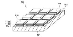
図1は、半導体基板100の構成例を示す斜視図である。半導体基板100は、1枚のベース基板101に複数の単結晶半導体層116が貼り付けられている。各単結晶半導体層116は絶縁層102を介してベース基板101に設けられており、半導体基板100は、いわゆるSOI構造の基板である。
FIG. 1 is a perspective view illustrating a configuration example of the
絶縁層102は、単層構造でも積層構造でもよい。本実施の形態では絶縁層102は3層構造であり、ベース基板101側から、接合層114、窒化酸化シリコン層である絶縁膜112b、酸化窒化シリコン層である絶縁膜112aが積層されている。
The
単結晶半導体層116は、単結晶半導体基板を薄膜化することで形成される層である。単結晶半導体基板には、市販の半導体基板を用いることができ、例えば、単結晶シリコン基板、単結晶ゲルマニウム基板、単結晶シリコンゲルマニウム基板など、第4族元素でなる単結晶半導体基板を用いることができる。また、ガリウムヒ素やインジウムリン等の化合物半導体基板も用いることができる。
The single
ベース基板101は、絶縁表面を有する基板を用いる。具体的には、アルミノシリケートガラス、アルミノホウケイ酸ガラス、バリウムホウケイ酸ガラスのような電子工業用に使われる各種ガラス基板、石英基板、セラミック基板、サファイア基板が挙げられる。好ましくはベース基板101としてガラス基板を用いるのがよい。ガラス基板には、熱膨張係数が25×10−7/℃以上50×10−7/℃以下(好ましくは、30×10−7/℃以上40×10−7/℃以下)であり、歪み点が580℃以上680℃以下(好ましくは、600℃以上680℃以下)である基板を用いることが好ましい。また、半導体装置の汚染を抑えるため、ガラス基板は無アルカリガラス基板が好ましい。無アルカリガラス基板の材料には、、例えば、アルミノシリケートガラス、アルミノホウケイ酸ガラス、バリウムホウケイ酸ガラスなどのガラス材料などがある。また、ベース基板101には、ガラス基板の他、セラミック基板、石英基板やサファイア基板などの絶縁体でなる絶縁性基板、金属やステンレスなどの導電体でなる導電性基板、シリコンやガリウムヒ素など半導体でなる半導体基板などを用いることができる。
As the
ガラス基板としては、液晶パネルの製造用に開発されたマザーガラス基板を用いることが好ましい。マザーガラスとしては、例えば、第3世代(550mm×650mm)、第3.5世代(600mm×720mm)、第4世代(680mm×880mmまたは、730mm×920mm)、第5世代(1100mm×1300mm)第6世代(1500mm×1850mm)、第7世代(1870mm×2200mm)、第8世代(2200mm×2400mm)などのサイズの基板が知られている。大面積のマザーガラス基板をベース基板101として用いてSOI基板を製造することで、SOI基板の大面積化が実現できる。
As the glass substrate, it is preferable to use a mother glass substrate developed for manufacturing liquid crystal panels. As the mother glass, for example, the third generation (550 mm × 650 mm), the third generation (600 mm × 720 mm), the fourth generation (680 mm × 880 mm or 730 mm × 920 mm), the fifth generation (1100 mm × 1300 mm) Substrates of sizes such as 6th generation (1500 mm × 1850 mm), 7th generation (1870 mm × 2200 mm), 8th generation (2200 mm × 2400 mm) are known. By manufacturing an SOI substrate using a large-area mother glass substrate as the
マザーガラス基板のような大面積な基板をベース基板101として用いることで、SOI基板の大面積化が実現できる。SOI基板の大面積化が実現すれば、一度に多数のIC、LSI等のチップを製造することができ、1枚の基板から製造されるチップ数が増加するので、生産性を飛躍的に向上させることができる。
By using a large substrate such as a mother glass substrate as the
以下、図2〜図10を参照して、図1に示す半導体基板100の作製方法を説明する。
A method for manufacturing the
まず、単結晶半導体基板110を準備する。単結晶半導体基板110は、所望の大きさ、形状に加工されている。図2は、単結晶半導体基板110の構成の一例を示す斜視図である。矩形状のベース基板101に貼り合わせること、および縮小投影型露光装置などの露光装置の露光領域が矩形であること等を考慮すると、図2に示すように単結晶半導体基板110の形状は矩形であることが好ましい。なお、特段の断りが無い限り、矩形には正方形が含まれることとする。例えば、矩形状の単結晶半導体基板110の長辺の長さは、縮小投影型露光装置の1ショットの露光領域の一辺のn倍(nは任意の正の整数で、n≧1)を満たすように加工することが好ましい。
First, a single
矩形の単結晶半導体基板110は、市販の円形状のバルク単結晶半導体基板を切断することで形成することができる。基板の切断には、ダイサー或いはワイヤソー等の切断装置、レーザ切断、プラズマ切断、電子ビーム切断、その他任意の切断手段を用いることができる。また、基板として薄片化する前の半導体基板製造用のインゴットを、その断面が矩形になるように直方体状に加工し、この直方体状のインゴットを薄片化することでも、矩形状の単結晶半導体基板110を製造することができる。
The rectangular single
単結晶半導体基板110を洗浄した後、トレイ10に複数の単結晶半導体基板110を配置する。図3は、トレイ10の構成の一例を示す斜視図である。トレイ10は、板状の部材であり、単結晶半導体基板110を保持するための複数の凹部11が形成されている。図3は、図1の半導体基板100を製造するためのトレイであり、3行3列に凹部11が形成されている。図4に示すように、凹部11に収めるように単結晶半導体基板110をトレイ10に並べる。
After the single
トレイ10は、半導体基板100の基板の作製工程での熱処理で変質、変形しない材料で作製される。特に、熱処理での熱膨張が少ない材料を選択することが好ましい。例えば、石英ガラス、ステンレス、無アルカリガラスなどでトレイ10を作製することができる。
The
トレイ10の厚さは、1.1mm以上2mm以下とすることができる。凹部11の深さは、0.2mm以上0.6mm以下とすることができ、0.3mm以上0.5mm以下が好ましい。トレイ10のサイズは、ベース基板101と同じサイズとすることが好ましい。凹部11のサイズは、半導体基板100が収まるサイズであればよい。なお本実施の形態の作製方法では、図4に示すように、凹部11のサイズおよび配列によって、半導体基板100の単結晶半導体層116のサイズ、配列が制約される。
The thickness of the
図5、図6は、トレイ10の構成例を示す上面図である。図5は、ベース基板101に、サイズが600mm×720mmであるマザーガラス基板を用いる場合のトレイ10の平面図であり、トレイ10のサイズは600mm×720mmである。図6は、ベース基板101に、サイズが730mm×920mmである第4世代のマザーガラス基板を用いる場合のトレイ10の平面図であり、トレイ10のサイズは730mm×920mmである。
5 and 6 are top views showing examples of the configuration of the
図5(A)は、露光領域のサイズが4インチ角の縮小投影型露光装置に対応するように、凹部11のサイズおよび配置を考慮したトレイ10の平面図である。トレイ10は4つのブロックに区分されており、各ブロックには3行3列に配置された9つの凹部11が形成されている。各凹部11のサイズは1ショットの露光領域に収まる102mm×82mmである。1ブロックにおいて、凹部11どうしの間隔は、縦、横共に11mmであり、トレイ10の縁から凹部11までの距離は、縦、横共に16mmである。
FIG. 5A is a plan view of the
図5(B)は、露光領域のサイズが5インチ角の縮小投影型露光装置に対応するように、凹部11のサイズおよび配置を考慮したトレイ10の平面図である。トレイ10は4つのブロックに区分されており、各ブロックには3行2列に配置された6つの凹部11が形成されている。各凹部11のサイズは1ショットの露光領域に収まる102mm×130mmである。一ブロックにおいて、凹部11どうしの間隔は、縦は11mmであり横は10mmであり、トレイ10の縁から凹部11までの距離は、縦、横共に16mmである。
FIG. 5B is a plan view of the
図6(A)は、露光領域のサイズが4インチ角の縮小投影型露光装置に対応するように、凹部11のサイズおよび配置を考慮したトレイ10の平面図である。トレイ10は6つのブロックに区分されており、各ブロックには3行3列に配置された9つの凹部11が形成されている。各凹部11のサイズは1ショットの露光領域に収まる105mm×84mmである。一ブロックにおいて、凹部11どうしの間隔は、縦は11mmであり、横は10mmであり、トレイ10の縁から凹部11までの距離は、縦は16mmであり、横は15mmである。
FIG. 6A is a plan view of the
図6(B)は、露光領域のサイズが5インチ角の縮小投影型露光装置に対応するように、凹部11のサイズおよび配置を考慮したトレイ10の平面図である。トレイ10は6つのブロックに区分されており、各ブロックには2行3列に配置された6つの凹部11が形成されている。各凹部11のサイズは1ショットの露光領域に収まる132mm×105mmである。一ブロックにおいて、凹部11の間隔は、縦は13mmであり横は10mmであり、トレイ10の縁から凹部11までの距離は、縦、横共に15mmである。
FIG. 6B is a plan view of the
図3に示すように、トレイ10に単結晶半導体基板110を配置した後、次に、図7(A)に示すように、単結晶半導体基板110上に絶縁層112を形成する。絶縁層112は単層構造、2層以上の多層構造とすることができる。その厚さは5nm以上400nm以下とすることができる。絶縁層112を構成する膜には、酸化シリコン膜、窒化シリコン膜、酸化窒化シリコン膜、窒化酸化シリコン膜、酸化ゲルマニウム、窒化ゲルマニウム膜、酸化窒化ゲルマニウム膜、窒化酸化ゲルマニウム膜などのシリコンまたはゲルマニウムを組成に含む絶縁膜を用いることができる。また、酸化アルミニウム、酸化タンタル、酸化ハフニウムなどの金属の酸化物でなる絶縁膜、窒化アルミニウムなどの金属の窒化物でなる絶縁膜、酸化窒化アルミニウム膜などの金属の酸化窒化物でなる絶縁膜、窒化酸化アルミニウム膜などの金属の窒化酸化物でなる絶縁膜を用いることもできる。
As shown in FIG. 3, after the single
なお、本明細書において、酸化窒化物とは、その組成として、窒素原子よりも酸素原子の数が多い物質とし、また、窒化酸化物とは、その組成として、酸素原子より窒素原子の数が多い物質とする。例えば、酸化窒化シリコンとは、酸素が55〜65原子%、窒素が1〜20原子%、Siが25〜35原子%、水素が0.1〜10原子%の範囲で含まれる物質とする。また、窒化酸化シリコンとは、酸素が15〜30原子%、窒素が20〜35原子%、Siが25〜35原子%、水素が15〜25原子%の範囲で含まれる物質とする。 Note that in this specification, oxynitride is a substance having a larger number of oxygen atoms than nitrogen atoms, and nitride oxide is a composition having a number of nitrogen atoms greater than oxygen atoms. Use many substances. For example, silicon oxynitride is a substance containing oxygen in the range of 55 to 65 atomic%, nitrogen in the range of 1 to 20 atomic%, Si in the range of 25 to 35 atomic%, and hydrogen in the range of 0.1 to 10 atomic%. Silicon nitride oxide is a substance containing 15 to 30 atomic% of oxygen, 20 to 35 atomic% of nitrogen, 25 to 35 atomic% of Si, and 15 to 25 atomic% of hydrogen.
絶縁層112を構成する絶縁膜は、CVD法、スパッタ法、単結晶半導体基板110を酸化するまたは窒化するなどの方法により形成することができる。
The insulating film included in the insulating
ベース基板101にアルカリ金属若しくはアルカリ土類金属などの半導体装置の信頼性を低下させる不純物を含むような基板を用いた場合、このような不純物がベース基板101から、SOI基板の半導体層に拡散することを防止できるような膜を少なくとも1層以上、絶縁層112に設けることが好ましい。このような膜には、窒化シリコン膜、窒化酸化シリコン膜、窒化アルミニウム膜、または窒化酸化アルミニウム膜などがある。このような膜を含ませることで、絶縁層112をバリア層として機能させることができる。
In the case where a substrate containing an impurity such as an alkali metal or an alkaline earth metal that decreases the reliability of a semiconductor device is used as the
例えば、絶縁層112を単層構造のバリア層として形成する場合、厚さ5nm以上200nm以下の窒化シリコン膜、窒化酸化シリコン膜、窒化アルミニウム膜、または窒化酸化アルミニウム膜で形成することができる。
For example, when the insulating
絶縁層112を、バリア層として機能する2層構造の膜とする場合は、上層は、バリア機能の高い絶縁膜で構成する。上層は、厚さ5nm〜200nmの窒化シリコン膜、窒化酸化シリコン膜、窒化アルミニウム膜、または窒化酸化アルミニウム膜で形成することができる。これらの膜は、不純物の拡散を防止するブロッキング効果が高いが、内部応力が高い。そのため、単結晶半導体基板110と接する下層の絶縁膜には、上層の絶縁膜の応力を緩和する効果のある膜を選択することが好ましい。このような絶縁膜には、酸化シリコン膜および酸化シリコン膜、および単結晶半導体基板110を熱酸化して形成した熱酸化膜などがある。下層の絶縁膜の厚さは5nm以上300nm以下とすることができる。
In the case where the insulating
本実施の形態では、絶縁層112を絶縁膜112aと絶縁膜112bでなる2層構造とする。絶縁層112をブロッキング膜として機能させる絶縁膜112aと絶縁膜112bの組み合わせは、例えば、酸化シリコン膜と窒化シリコン膜、酸化窒化シリコン膜と窒化シリコン膜、酸化シリコン膜と窒化酸化シリコン膜、酸化窒化シリコン膜と窒化酸化シリコン膜などがある。
In this embodiment, the insulating
例えば、下層の絶縁膜112aは、プロセスガスにSiH4およびN2Oを用いてプラズマ励起CVD法(以下、「PECVD法」という。)で形成した酸化窒化シリコン膜で形成することができる。また、絶縁膜112aとして、プロセスガスに有機シランガスと酸素を用いて、PECVD法で酸化シリコン膜を形成することもできる。また、単結晶半導体基板110を酸化した、酸化膜で絶縁膜112aを形成することもできる。
For example, the lower insulating
有機シランとは、珪酸エチル(TEOS:化学式Si(OC2H5)4)、テトラメチルシラン(TMS:化学式Si(CH3)4)、テトラメチルシクロテトラシロキサン(TMCTS)、オクタメチルシクロテトラシロキサン(OMCTS)、ヘキサメチルジシラザン(HMDS)、トリエトキシシラン(SiH(OC2H5)3)、またはトリスジメチルアミノシラン(SiH(N(CH3)2)3)などの化合物である。 Organosilanes are ethyl silicate (TEOS: chemical formula Si (OC 2 H 5 ) 4 ), tetramethylsilane (TMS: chemical formula Si (CH 3 ) 4 ), tetramethylcyclotetrasiloxane (TMCTS), octamethylcyclotetrasiloxane. (OMCTS), hexamethyldisilazane (HMDS), triethoxysilane (SiH (OC 2 H 5 ) 3 ), or trisdimethylaminosilane (SiH (N (CH 3 ) 2 ) 3 ).
上層の絶縁膜112bは、プロセスガスにSiH4、N2O、NH3およびH2を用いてPECVD法で形成した窒化酸化シリコン膜で形成することができる。プロセスガスにSiH4、N2、NH3およびH2を用いてPECVD法で形成した窒化シリコン膜で形成することができる。
The upper
例えば、PECVD法で、窒化酸化シリコンでなる絶縁膜112a、酸化窒化シリコンでなる絶縁膜112aを形成する場合、トレイ10に配置された複数の単結晶半導体基板110をPECVD装置の処理室に搬入し、SiH4、N2O、NH3およびH2のガスのプラズマを生成し、窒化酸化シリコン膜を単結晶半導体基板110上に形成する。次いで、処理室に導入するガスをSiH4およびN2Oに変更し、これらの混合ガスのプラズマを生成して、窒化酸化シリコン膜上に酸化窒化シリコン膜を連続して形成する。また、複数の処理室を有するPECVD装置を用いる場合は、窒化酸化シリコン膜と酸化窒化シリコン膜と異なる処理室で形成することもできる。もちろん、処理室に導入するガスを変更することで、下層に酸化シリコン膜を形成することもできるし、上層に窒化シリコン膜を形成することもできる。
For example, when the insulating
上記のように絶縁膜112aおよび絶縁膜112bを形成することで、スループット良く、複数の単結晶半導体基板110に絶縁層112を形成することができる。また、大気に触れさせることなく絶縁膜112a、絶縁膜112bを形成できるので、絶縁膜112aと絶縁膜112bの界面が大気によって汚染されることを防止することができる。
By forming the insulating
また、絶縁膜112aを、単結晶半導体基板110を酸化処理することで得られる酸化膜で形成することができる。この酸化膜を形成するための、熱酸化処理には、ドライ酸化でも良いが、酸化雰囲気中にハロゲンを含むガスを添加することが好ましい。ハロゲンを含むガスとして、HCl、HF、NF3、HBr、Cl、ClF、BCl3、F、Br2などから選ばれた一種又は複数種ガスを用いることができる。
The insulating
例えば、酸素に対しHClを0.5〜10体積%(好ましくは3体積%)の割合で含む雰囲気中で、700℃以上の温度で熱処理を行う。950℃以上1100℃以下の加熱温度で熱酸化を行うとよい。処理時間は0.1〜6時間、好ましくは0.5〜1時間とすればよい。形成される酸化膜の膜厚は、10nm〜1000nm(好ましくは50nm〜200nm)、例えば100nmの厚さとすることができる。 For example, heat treatment is performed at a temperature of 700 ° C. or higher in an atmosphere containing HCl at 0.5 to 10% by volume (preferably 3% by volume) with respect to oxygen. Thermal oxidation may be performed at a heating temperature of 950 ° C. or higher and 1100 ° C. or lower. The treatment time may be 0.1 to 6 hours, preferably 0.5 to 1 hour. The thickness of the oxide film to be formed can be 10 nm to 1000 nm (preferably 50 nm to 200 nm), for example, 100 nm.
このような温度範囲で酸化処理を行うことで、ハロゲン元素によるゲッタリング効果を得ることができる。ゲッタリングとしては、特に、金属不純物を除去する効果がある。すなわち、塩素の作用により、金属などの不純物が揮発性の塩化物となって気相中へ離脱して、単結晶半導体基板110から除去される。また、酸化処理に含まれるハロゲン元素により、単結晶半導体基板110の表面の欠陥が終端化されるため、酸化膜と単結晶半導体基板110との界面の局在準位密度が低減できる。
By performing oxidation treatment in such a temperature range, a gettering effect by a halogen element can be obtained. Gettering is particularly effective in removing metal impurities. In other words, due to the action of chlorine, impurities such as metals are converted into volatile chlorides and separated into the gas phase, and are removed from the single
このハロゲンを含む雰囲気での熱酸化処理により、酸化膜にハロゲンを含ませることができる。ハロゲン元素を1×10¹⁷atoms/cm3〜5×1020atoms/cm3の濃度で含ませることにより、半導体基板100において、金属などの不純物を捕獲して単結晶半導体層116の汚染を防止する保護膜としての機能を発現させることができる。
By thermal oxidation treatment in an atmosphere containing halogen, the oxide film can contain halogen. By containing a halogen element at a concentration of 1 × 10 17 atoms / cm 3 to 5 × 10 20 atoms / cm 3 , the
熱酸化処理で下層の絶縁膜112aを形成し、PECVD法などの気相法で上層の絶縁膜112bを形成する場合は、単結晶半導体基板110をトレイ10に配置するまえに、熱酸化処理で絶縁膜112aを形成し、酸化膜でなる絶縁膜112aが形成された単結晶半導体基板110をトレイ10に並べ、しかる後に絶縁膜112bを形成することもできる。
In the case where the lower insulating
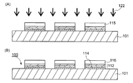
次に、図7(B)に示すように、絶縁層112を介して、電界で加速されたイオンでなるイオンビーム121を単結晶半導体基板110にドーピングして、注入して、単結晶半導体基板110の表面から所定の深さの領域に、損傷領域113を形成する。損傷領域113が形成される領域の深さは、イオンビーム121の加速エネルギーとイオンビーム121の入射角によって調節することができる。加速エネルギーは加速電圧、ドーズ量などにより調節できる。イオンの平均侵入深さとほぼ同じ深さの領域に損傷領域113が形成される。イオンを注入する深さで、単結晶半導体基板110から分離される半導体層の厚さが決定される。損傷領域113が形成される深さは50nm以上500nm以下であり、好ましい深さの範囲は50nm以上200nm以下である。
Next, as illustrated in FIG. 7B, an
イオンを単結晶半導体基板110にドーピングするには、質量分離を伴うイオン注入法よりも、素子量分離を伴わないイオンドーピング法が好ましい。これにより、大面積なトレイ10に配置された複数の単結晶半導体基板110に損傷領域113を形成するタクトタイムを短縮できるからである。
In order to dope ions into the single
トレイ10に収められた単結晶半導体基板110を、イオンドーピング装置の処理室に搬入する。プロセスガスを励起しプラズマを生成し、そのプラズマから所望のイオンを引き出し、加速してイオンビーム121生成し、そのイオンビーム121を、複数の単結晶半導体基板110に照射することで、所定の深さにイオンが高濃度に導入され、損傷領域113が形成される。
The single
ソースガスに水素(H2)を用いる場合、水素ガスを励起してH+、H2 +、H3 +を生成することができる。ソースガスから生成されるイオン種の割合は、プラズマの励起方法、プラズマを発生させる雰囲気の圧力、ソースガスの供給量などを調節することで、変化させることができる。イオンドーピング法でイオン注入を行う場合、イオンビーム121に、H+、H2 +、H3 +の総量に対してH3 +が70%以上含まれるようにすることが好ましく、H3 +の割合は80%以上がより好ましい。H3 +の割合を70%以上とすることで、イオンビーム121に含まれるH2 +イオンの割合が相対的に小さくなるため、イオンビーム121に含まれる水素イオンの平均侵入深さのばらつきが小さくなるので、イオンの注入効率が向上し、タクトタイムを短縮することができる。
When hydrogen (H 2 ) is used for the source gas, the hydrogen gas can be excited to generate H + , H 2 + , and H 3 + . The ratio of ion species generated from the source gas can be changed by adjusting the plasma excitation method, the pressure of the atmosphere in which the plasma is generated, the supply amount of the source gas, and the like. When performing ion implantation by an ion doping method, an ion beam 121, H +, H 2 + , preferably the amount of H 3 + to be included more than 70% of the total amount of H 3 +, H 3 + in The ratio is more preferably 80% or more. By setting the ratio of H 3 + to 70% or more, the ratio of H 2 + ions contained in the
また、H3 +はH+、H2 +に比べて質量が大きい。そのため、イオンビーム121において、H3 +の割合が多い場合と、H+、H2 +の割合が多い場合とでは、ドーピングの際の加速電圧が同じであっても、前者の場合の方が、単結晶半導体基板110の浅い領域に水素を注入することができる。また前者の場合、単結晶半導体基板110に注入される水素の、厚さ方向における濃度分布が急峻となるため、損傷領域113の厚さ自体も薄くすることができる。
Further, H 3 + has a larger mass than H + and H 2 + . Therefore, in the
水素ガスを用いて、イオンドーピング法でイオン注入を行う場合、加速電圧10kV以上200kV以下、ドーズ量1×10¹⁶ions/cm2以上6×1016ions/cm2以下とすることができる。この条件で水素イオンを注入することで、イオンビーム121に含まれるイオン種および、その割合にもよるが、損傷領域113を単結晶半導体基板110の深さ50nm以上500nm以下の領域に形成することができる。
When ion implantation is performed using hydrogen gas by an ion doping method, an acceleration voltage of 10 kV to 200 kV and a dose of 1 × 10 16 ions / cm 2 to 6 × 10 16 ions / cm 2 can be set. By implanting hydrogen ions under these conditions, the damaged
例えば、単結晶半導体基板110が単結晶シリコン基板であり、絶縁膜112aが厚さ50nmの酸化窒化シリコン膜であり、絶縁膜112bが厚さ50nmの窒化酸化シリコン膜の場合、ソースガスが水素であり、加速電圧40kV、ドーズ量2.2×10¹⁶ions/cm2の条件では、単結晶半導体基板110から厚さ120nm程度の単結晶半導体層を剥離することができる。また、絶縁膜112aを厚さ100nmの酸化窒化シリコン膜とし、他は同じ条件で水素イオンをドープすると、単結晶半導体基板110から厚さ70nm程度の半導体層を剥離することができる。
For example, when the single
イオンビーム121のソースガスにヘリウム(He)を用いることもできる。ヘリウムを励起して生成されるイオン種がHe+が殆どであるため、質量分離を伴わないイオンドーピング法でも、He+を主たるイオンとして単結晶半導体基板110に注入することができる。よって、イオンドーピング法で、効率良く、微小な空孔を損傷領域113に形成することができる。ヘリウムを用いて、イオンドーピング法でイオン注入を行う場合、加速電圧10kV以上200kV以下、ドーズ量1×10¹⁶ions/cm2以上6×1016ions/cm2以下とすることができる。
Helium (He) can also be used for the source gas of the
ソースガスに塩素ガス(Cl2ガス)、フッ素ガス(F2ガス)などのハロゲンガスを用いることもできる。 A halogen gas such as chlorine gas (Cl 2 gas) or fluorine gas (F 2 gas) can also be used as the source gas.
なお、イオンドーピング法では質量分離を行わずにイオンを電界で加速して半導体に打ち込むので、イオンドーピングを行う装置内の金属、化合物などの不純物がイオンと共に半導体に打ち込まれてしまうことがある。よって、イオンドーピング法で単結晶半導体基板110にイオン注入を行う場合、上記不純物が最表面の絶縁膜112bに存在する可能性がある。この場合、絶縁膜112bの表面をエッチングし、不純物を除去しても良い。
In the ion doping method, ions are accelerated by an electric field without mass separation and are implanted into the semiconductor, so that impurities such as metals and compounds in the apparatus for performing ion doping may be implanted into the semiconductor together with the ions. Therefore, when ion implantation is performed on the single
損傷領域113を形成した後、絶縁層112の上面に、図7(C)に示すように、接合層114を形成する。接合層114を形成する工程では、単結晶半導体基板110の加熱温度は。損傷領域113に注入した元素または分子が析出しない温度とし、その加熱温度は350℃以下が好ましい。言い換えると、この加熱温度は損傷領域113からガスが抜けない温度である。なお、接合層114は、イオン注入工程を行う前に形成することもできる。この場合は、接合層114を形成するときのプロセス温度は、350℃以上にすることができる。
After the damaged
接合層114は、平滑で親水性の接合面を単結晶半導体基板110の表面に形成するため層である。そのため、接合層114の平均粗さRaが0.7nm以下、より好ましくは、0.4nm以下が好ましい。また、接合層114の厚さは10nm以上200nm以下とすることができる。好ましい厚さは5nm以上500nm以下であり、より好ましくは10nm以上200nm以下である。
The
接合層114には、化学的気相反応により形成される絶縁膜が好ましく、酸化シリコン膜が好ましい。接合層114として、プラズマ励起CVD法で酸化シリコン膜を形成する場合には、ソースガスに有機シランガスおよび酸素(O2)ガスを用いることが好ましい。ソースガスに有機シランを用いることで、プロセス温度が350℃以下で、平滑な表面を有する酸化シリコン膜を形成することができる。また、熱CVD法で、加熱温度が500℃以下200℃以上で形成されるLTO(低温酸化物、low temperature oxide)で形成することができる。LTOの形成には、シリコンソースガスにモノシラン(SiH4)またはジシラン(Si2H6)などを用い、酸素ソースガスに一酸化二窒素(N2O)などを用いることができる。
The
例えば、ソースガスにTEOSとO2を用いて、酸化シリコン膜でなる接合層114を形成するための条件例としては、処理室に、流量15sccmでTEOSを導入し、流量750sccmでO2を導入する。成膜圧力は100Pa、成膜温度300℃、RF出力300W、電源周波数13.56MHzが挙げられる。
For example, as a condition example for forming the
なお、有機シランを用いて形成された酸化シリコン膜、または低温で成膜した窒化酸化シリコン膜などの、比較的低温で成膜された接合層は、表面にOH基を多く有する。OH基は水分子と水素結合することでシラノール基を形成して、ベース基板と接合層とを低温で接合する。そして、最終的には共有結合であるシロキサン結合が、ベース基板と接合層との間に形成される。よって、上記の有機シランを用いて形成された酸化シリコン膜または低温で成膜した窒化酸化シリコン膜などの比較的低温で成膜された接合層は、Smart Cutなどで用いられているOH基を内在しない或いは飛躍的に少ない熱酸化膜よりも、低温での接合に向いていると言える。 Note that a bonding layer formed at a relatively low temperature such as a silicon oxide film formed using organosilane or a silicon nitride oxide film formed at a low temperature has many OH groups on the surface. The OH group forms a silanol group by hydrogen bonding with a water molecule, and bonds the base substrate and the bonding layer at a low temperature. Finally, a siloxane bond that is a covalent bond is formed between the base substrate and the bonding layer. Therefore, a bonding layer formed at a relatively low temperature such as a silicon oxide film formed using organosilane or a silicon nitride oxide film formed at a low temperature has an OH group used in Smart Cut or the like. It can be said that it is suitable for bonding at a low temperature rather than a thermal oxide film that is not inherently or drastically reduced.
次に、絶縁層112および接合層114が形成された単結晶半導体基板110をトレイ10からはずし、複数の単結晶半導体基板110を洗浄する。この洗浄工程は、純水による超音波洗浄で行うことができる。超音波洗浄はメガヘルツ超音波洗浄(メガソニック洗浄)が好ましい。超音波洗浄の後、単結晶半導体基板110をオゾン水で洗浄してもよい。オゾン水で洗浄することで、有機物の除去と、接合層114表面の親水性を向上させる表面活性化処理を行うことができる。洗浄処理、および表面活性化処理の終了後、図7(D)に示すように単結晶半導体基板110をトレイ10の凹部11に配置する。
Next, the single
接合層114の表面の活性化処理には、オゾン水による洗浄の他原子ビーム若しくはイオンビームの照射処理、プラズマ処理、若しくはラジカル処理で行うことができる。原子ビーム若しくはイオンビームを利用する場合には、アルゴン等の不活性ガス中性原子ビーム若しくは不活性ガスイオンビームを用いることができる。これらの処理は、単結晶半導体基板110をトレイ10に配置した状態で行うこともできる。
The surface activation treatment of the
次に、トレイ10に配置された単結晶半導体基板110とベース基板101を貼り合わせる。貼り合わせる前に、ベース基板101も洗浄する。塩酸と過酸化水素水を用いた洗浄や、メガヘルツ超音波洗浄で行うことができる。また、ベース基板101の接合面となる表面を、接合層114と同様な処理で、表面活性化処理を行うことが好ましい。
Next, the single
また、EAGLE2000(コーニング社製)等のように、加熱処理を加えることで大きくシュリンクするようなガラス基板をベース基板101として用いる場合、接合工程後に貼り合わせの不良が生じる場合がある。よって、シュリンクに起因する貼り合わせの不良を回避するために、次に示す接合工程に移る前に、ベース基板101に予め加熱処理を施しておいても良い。
In addition, when a glass substrate that shrinks greatly by applying heat treatment, such as EAGLE 2000 (manufactured by Corning), is used as the
図8(A)は接合工程を説明する断面図である。複数の単結晶半導体基板110が配置されたトレイ10の上方からベース基板101を載置する。ベース基板101の端の一箇所に300〜15000N/cm2程度の圧力を加える。この圧力は、1000〜5000N/cm2が好ましい。圧力をかけた部分から接合層114とベース基板101とが密着し始める。やがて1枚のベース基板101に対して、トレイ10上の全ての単結晶半導体基板110が密着する。この接合工程は、加熱処理を伴わず、常温で行うことができるため、ベース基板101に、ガラス基板など耐熱性の低い基板を用いることが可能である。
FIG. 8A is a cross-sectional view illustrating a bonding process. A
複数の単結晶半導体基板110基板をトレイ10に並べているため、単結晶半導体基板110の厚さの違いにより、接合層114の表面がベース基板101と接触しない単結晶半導体基板110が生じる場合がある。そのため、圧力をかける場所は一箇所ではなく、各単結晶半導体基板110に圧力をかけるようにすることが好ましい。また、トレイ10に配置された状態で、接合層114表面の高さが多少違っていても、ベース基板101のたわみにより接合層114の一部分がベース基板101と密着すれば、接合層114表面全体に接合が進行することが可能である。
Since the plurality of single
また、図8(A)のようにベース基板101をトレイ10に載せた後、図9のように、ベース基板101を下側に入れ替え得ることで、単結晶半導体基板110の厚さの違いが相殺され、接合層114の表面全体をベース基板101の表面に容易に接触させることができる。
Further, after the
ベース基板101に単結晶半導体基板110を貼り合わせた後、ベース基板101と接合層114との接合界面での結合力を増加させるための加熱処理を行うことが好ましい。この処理温度は、損傷領域113に亀裂を発生させない温度とし、200℃以上450℃以下の温度範囲で処理することができる。また、この温度範囲で加熱しながら、ベース基板101に単結晶半導体基板110を貼り合わせることで、ベース基板101と接合層114との接合界面での結合力を強固にすることができる。
After the single
図8(A)に示すように、トレイ10に配置された単結晶半導体基板110上にベース基板101を載置するときに、接合面にゴミなどにより汚染されてしまうと、汚染部分は接合されなくなる。そのため、接合面の汚染を防ぐため、ベース基板101を載置するときは、気密な処理室内で行うことが好ましい。また、処理室内を5.0×10⁻³Pa程度の減圧状態とし、接合処理の雰囲気を清浄にすることが好ましい。
As shown in FIG. 8A, when the
次いで、加熱処理を行い、損傷領域113で剥離を生じさせて、単結晶半導体基板110から単結晶半導体層115を分離する。図8(B)は、単結晶半導体基板110から単結晶半導体層115を分離する分離工程を説明する図である。117を付した要素は、単結晶半導体層115が分離された単結晶半導体基板110を示している。
Next, heat treatment is performed to cause separation in the damaged
なお、図8(B)に示すように、単結晶半導体基板110の周辺部がベース基板101に接合しない場合が多くある。これは、単結晶半導体基板110の周辺部が面取りされている、或いは周辺部が曲率を有しているため、ベース基板101と接合層104とが密着しない、単結晶半導体基板110の周辺部では損傷領域113が分割しにくいなどの理由によるものと考えられる。また、その他の理由として、単結晶半導体基板110を作製する際に行われるCMPなどの研磨が、単結晶半導体基板110の周辺部で不十分であり、中央部に比べて周辺部では表面が荒れていることが挙げられる。また、単結晶半導体基板110をトレイ10に並べる際に、キャリア等で単結晶半導体基板110の周辺部に傷が入ってしまった場合、該傷も、周辺部がベース基板101に接合しにくい理由になると考えられる。そのため、ベース基板101には、単結晶半導体基板110よりもサイズが小さい単結晶半導体層115が貼り付けられ、また、単結晶半導体基板117の周囲には凸部が形成され、その凸部上に、ベース基板101に貼り付けられなかった、絶縁膜112b、絶縁膜112aおよび接合層114が残っている。
Note that as illustrated in FIG. 8B, the periphery of the single
加熱処理を行うことで、温度上昇によって、損傷領域113に形成されている微小な孔には、イオンドーピングで添加した元素が析出し、内部の圧力が上昇する。圧力の上昇により、損傷領域113の微小な孔に体積変化が起こり、損傷領域113に亀裂が生じるので、損傷領域113沿って単結晶半導体基板110が劈開される。接合層114はベース基板101に接合しているので、ベース基板101上には単結晶半導体基板110から分離された単結晶半導体層115が固定される。単結晶半導体層115を単結晶半導体基板110から分離するための加熱処理の温度は、ベース基板101の歪み点を越えない温度とする。
By performing the heat treatment, the element added by ion doping is deposited in the minute hole formed in the damaged
この加熱処理には、RTA(Rapid Thermal Anneal)装置、抵抗加熱炉、マイクロ波加熱装置を用いることができる。RTA装置には、GRTA(Gas Rapid Thermal Anneal)装置、LRTA(Lamp Rapid Thermal Anneal)装置を用いることができる。 For this heat treatment, a rapid thermal annealing (RTA) device, a resistance heating furnace, or a microwave heating device can be used. As the RTA apparatus, a GRTA (Gas Rapid Thermal Anneal) apparatus or an LRTA (Lamp Rapid Thermal Anneal) apparatus can be used.
GRTA装置を用いる場合は、加熱温度550℃以上650℃以下、処理時間0.5分以上60分以内とすることができる。抵抗加熱装置を用いる場合は、加熱温度200℃以上650℃以下、処理時間2時間以上4時間以内とすることができる。マイクロ波処理装置を用いる場合は、マイクロ波周波数2.45GHzとし、処理時間10分以上20分以内とすることができる。 When a GRTA apparatus is used, the heating temperature can be 550 ° C. or higher and 650 ° C. or lower, and the treatment time can be 0.5 minutes or longer and 60 minutes or less. In the case of using a resistance heating device, the heating temperature can be 200 ° C. or more and 650 ° C. or less, and the treatment time can be 2 hours or more and 4 hours or less. In the case of using a microwave processing apparatus, the microwave frequency can be set to 2.45 GHz, and the processing time can be 10 minutes or more and 20 minutes or less.
抵抗加熱を有する縦型炉を用いた加熱処理の具体的な処理方法を説明する。トレイ10に配置された単結晶半導体基板110が貼り付けられたベース基板101を、縦型炉のボートに載置する。ボートを縦型炉のチャンバーに搬入する。単結晶半導体基板110の酸化を抑制するため、まずチャンバー内を排気して真空状態とする。真空度は、5×10⁻³Pa程度とする。真空状態にした後、窒素をチャンバー内に供給して、チャンバー内を大気圧の窒素雰囲気にする。この間、加熱温度を200℃に上昇させる。
A specific treatment method of heat treatment using a vertical furnace having resistance heating will be described. The
チャンバー内を大気圧の窒素雰囲気にした後、温度200℃で2時間加熱する。その後、1時間かけて400℃に温度上昇させる。加熱温度400℃の状態が安定したら、1時間かけて600℃に温度上昇させる。加熱温度600℃の状態が安定したら、600℃で2時間加熱処理する。その後、1時間かけて、加熱温度400℃まで下げ、10分〜30分間後に、チャンバー内からボートを搬出する。大気雰囲気下で、ボート上のトレイ10に並べられた単結晶半導体基板117、および単結晶半導体層115が貼り付けられたベース基板101を冷却する。
After making the inside of a chamber into nitrogen atmosphere of atmospheric pressure, it heats at 200 degreeC for 2 hours. Thereafter, the temperature is raised to 400 ° C. over 1 hour. When the heating temperature is stabilized at 400 ° C., the temperature is raised to 600 ° C. over 1 hour. When the state of the heating temperature of 600 ° C. is stabilized, heat treatment is performed at 600 ° C. for 2 hours. Thereafter, the heating temperature is lowered to 400 ° C. over 1 hour, and after 10 to 30 minutes, the boat is unloaded from the chamber. In an air atmosphere, the single
上記の抵抗加熱炉を用いた加熱処理は、接合層114とベース基板101との結合力を強化するための加熱処理と、損傷領域113を分割させる加熱処理が連続して行われる。この2つの加熱処理を異なる装置で行う場合は、例えば、抵抗加熱炉において、処理温度200℃、処理時間2時間の加熱処理を行った後、貼り合わされたベース基板101と単結晶半導体基板110を炉から搬出する。次いで、RTA装置で、処理温度600℃以上700℃以下、処理時間1分以上30分以下の加熱処理を行い、単結晶半導体基板110を損傷領域113で分割させる。
In the heat treatment using the resistance heating furnace, the heat treatment for strengthening the bonding force between the
次に本発明では、図8(C)に示すように、単結晶半導体層115をエッチングし、損傷領域113の分割により荒れてしまった単結晶半導体層115の表面を平坦化する。本実施の形態では、例えば反応性イオンエッチング(RIE:Reactive Ion Etching)法、ICP(Inductively Coupled Plasma)エッチング法、ECR(Electron Cyclotron Resonance)エッチング法、平行平板型(容量結合型)エッチング法、マグネトロンプラズマエッチング法、2周波プラズマエッチング法またはヘリコン波プラズマエッチング法等のドライエッチング法を用いる。
Next, in the present invention, as shown in FIG. 8C, the single
例えばICPエッチング法を用いる場合、エッチングガスである塩素の流量40sccm〜100sccm、コイル型の電極に投入する電力100W〜200W、下部電極(バイアス側)に投入する電力40W〜100W、反応圧力0.5Pa〜1.0Paとすれば良い。本実施の形態では、エッチングガスである塩素の流量100sccm、反応圧力1.0Pa、下部電極の温度70℃、コイル型の電極に投入するRF(13.56MHz)電力150W、下部電極(バイアス側)に投入する電力40W、エッチング時間25sec〜27secとし、単結晶半導体層115を50nm乃至60nm程度にまで薄膜化する。エッチングガスには、塩素、塩化硼素、塩化珪素または四塩化炭素などの塩素系ガス、四弗化炭素、弗化硫黄または弗化窒素などのフッ素系ガス、酸素などを適宜用いることができる。
For example, when using the ICP etching method, the flow rate of chlorine as an etching gas is 40 sccm to 100 sccm, the power is 100 W to 200 W applied to the coil-type electrode, the power is 40 W to 100 W applied to the lower electrode (bias side), and the reaction pressure is 0.5 Pa. It should just be set to -1.0Pa. In this embodiment, the flow rate of chlorine, which is an etching gas, is 100 sccm, the reaction pressure is 1.0 Pa, the temperature of the lower electrode is 70 ° C., the RF (13.56 MHz) power input to the coil electrode is 150 W, and the lower electrode (bias side) The single
上記エッチングにより、後に形成される半導体素子にとって最適となる膜厚まで単結晶半導体層115を薄膜化できるのみならず、単結晶半導体層115の表面を平坦化することができる。
By the etching, the single
なお、ベース基板101に密着された単結晶半導体層115は、損傷領域113の分離、および損傷領域113の形成によって、結晶欠陥が形成されている。また、その表面は平坦性が損なわれている。結晶欠陥を低減、および平坦性を向上するために、図10(A)に示す様に、単結晶半導体層115にレーザビーム122を照射する。
Note that the single
レーザビーム122を単結晶半導体層115側から照射することで、単結晶半導体層115上面から溶融させる。溶融した後、単結晶半導体層115が冷却、固化することで、図10(B)に示すように、その上面の平坦性が向上された単結晶半導体層116が形成される。図10(B)の斜視図が図1に対応する。
By irradiation with the
なお、レーザビーム122を照射する前に、ドライエッチングにより単結晶半導体層115の表面を平坦化している場合、ドライエッチングにより単結晶半導体層115の表面付近で結晶欠陥などの損傷が生じていることがある。しかし上記レーザビーム122の照射により、ドライエッチングにより生じる損傷をも補修することが可能である。
Note that in the case where the surface of the single
このレーザビームの照射工程では、レーザビーム122を用いているため、ベース基板101の温度上昇が抑えられるため、ガラス基板のような耐熱性の低い基板をベース基板101に用いることが可能になる。レーザビーム122の照射によって単結晶半導体層115は部分溶融させることが好ましい。完全溶融させると、液相となった単結晶半導体層115での無秩序な核発生により、単結晶半導体層115が再結晶化することとなり、単結晶半導体層115の結晶性が低下するからである。部分溶融させることで、単結晶半導体層115では、溶融されていない固相部分から結晶成長が進行する、いわゆる縦成長が起こる。縦成長による再結晶化によって、単結晶半導体層115の結晶欠陥が減少され、結晶性が回復される。なお、単結晶半導体層115が完全溶融状態であるとは、図10(A)の積層構造では、単結晶半導体層115が接合層114との界面まで溶融され、液体状態になっていることをいう。他方、単結晶半導体層115が部分溶融状態であるとは、上層が溶融して液相であり、下層が固相である状態をいう。
In this laser beam irradiation step, since the
レーザビーム122を発振するレーザ発振器は、その発振波長が、紫外光域乃至可視光域にあるものが選択される。レーザビームの122の波長は、単結晶半導体層115に吸収される波長とする。その波長は、レーザ光の表皮深さ(skin depth)などを考慮して決定することができる。例えば、波長は250nm以上700nm以下の範囲とすることができる。
As the laser oscillator that oscillates the
このレーザ発振器には、連続発振レーザ、疑似連続発振レーザ及びパルス発振レーザを用いることができる。部分溶融させるためパルス発振レーザが好ましい。例えば、パルス発振レーザの場合は、繰り返し周波数1MHz以下、パルス幅10n秒以上500n秒以下である。例えば、繰り返し周波数10Hz〜300Hz、パルス幅25n秒、波長308nmのXeClエキシマレーザを用いることができる。 As this laser oscillator, a continuous wave laser, a pseudo continuous wave laser, and a pulsed laser can be used. A pulsed laser is preferable for partial melting. For example, in the case of a pulsed laser, the repetition frequency is 1 MHz or less and the pulse width is 10 nsec or more and 500 nsec or less. For example, a XeCl excimer laser having a repetition frequency of 10 Hz to 300 Hz, a pulse width of 25 nsec, and a wavelength of 308 nm can be used.
また、レーザビーム122のエネルギーは、レーザビーム122の波長、レーザ光の表皮深さ、単結晶半導体層115の膜厚などを考慮して決定することができる。レーザビーム122のエネルギーは、例えば、300mJ/cm2以上800mJ/cm2以下の範囲とすることができ例えば、単結晶半導体層115の厚さが120nm程度であり、レーザ発振器にパルス発振レーザを用い、レーザビーム122の波長が308nmの場合は、レーザビーム122のエネルギー密度は600mJ/cm2〜700mJ/cm2とすることができる。
The energy of the
レーザビーム122の照射の雰囲気は、希ガスまたは窒素雰囲気のような不活性雰囲気、または真空状態で行うことが好ましい。できる。不活性雰囲気中でレーザビーム122を照射するには、気密性のあるチャンバー内でレーザビーム122を照射し、このチャンバー内の雰囲気を制御すればよい。チャンバーを用いない場合は、レーザビーム122の被照射面に窒素ガスなど不活性ガスを吹き付けることで不活性雰囲気でのレーザビーム122の照射を実現することができる。
The irradiation atmosphere of the
窒素などの不活性雰囲気や真空状態のほうが、大気雰囲気よりも単結晶半導体層116の平坦性を向上させる効果が高く、また、これらの雰囲気のほうが大気雰囲気よりもクラックやリッジの発生を抑える効果が高くなるため、レーザビーム122の使用可能なエネルギー範囲が広くなる。
An inert atmosphere such as nitrogen or a vacuum state has a higher effect of improving the flatness of the single
光学系により、レーザビーム122は、エネルギー分布を均一にし、かつ断面の形状を線状にすることが好ましい。このことにより、スループット良く、かつレーザビーム122の照射を均一に行うことができる。レーザビーム122のビーム長は、ベース基板101の1辺より長くすることで、1回の走査で、ベース基板101に貼り付けられた全ての単結晶半導体層115にレーザビーム122を照射することができる。レーザビーム122のビーム長がベース基板101の1辺より短い場合は、複数回の走査で、ベース基板101に貼り付けられた全ての単結晶半導体層115にレーザビーム122を照射することができるような、長さにすればよい。
By the optical system, it is preferable that the
なお、レーザビーム122を単結晶半導体層115に照射する前に、単結晶半導体層115の表面に形成されている自然酸化膜などの酸化膜を除去する処理を行う。酸化膜を除去するのは、単結晶半導体層115表面に酸化膜が残存した状態で、レーザビーム122を照射しても、平坦化の効果が十分に得られないからである。酸化膜の除去処理は、フッ酸水溶液で単結晶半導体層115を処理することで行うことができる。フッ酸による処理は、単結晶半導体層115の表面が撥水性を示すまで行うことが望ましい。撥水性を示すことで、単結晶半導体層115から酸化膜が除去されたことが確認できる。
Note that before the single
図10(A)のレーザビーム122の照射工程は、次のように行うことができる。まず、単結晶半導体層115を1/100に希釈されたフッ酸水溶液で110秒間処理して、表面の酸化膜を除去する。レーザビーム122のレーザ発振器として、XeClエキシマレーザ(波長:308nm、パルス幅:25n秒、繰り返し周波数60Hz)を用いる。光学系により、レーザビーム122の断面を300mm×0.34mmの線状に整形する。レーザビーム122の走査速度を2.0mm/秒とし、スキャンピッチを33μm、ビームショット数を約10ショットで、レーザビーム122を単結晶半導体層115に照射する。照射面に窒素ガスを吹き付けながら、レーザビーム122を走査する。ベース基板101が730mm×920mmの場合は、レーザビーム122のビーム長が300mmであるので、レーザビーム122の照射領域を3分割することで、ベース基板101に貼り付けられた全ての単結晶半導体層115にレーザビーム122を照射することができる。
The irradiation step with the
次に本発明では、図8(C)の場合と同様に、単結晶半導体層116の表面をエッチングしても良い。レーザビームの照射後に単結晶半導体層116の表面をエッチングする場合は、必ずしもレーザビームの照射を行う前に単結晶半導体層115の表面をエッチングする必要はない。また、レーザビームの照射を行う前に単結晶半導体層115の表面をエッチングした場合は、必ずしもレーザビームの照射後に単結晶半導体層116の表面をエッチングする必要はない。また本発明では、レーザビームの照射前と照射後の両方のタイミングでエッチングを行っても良い。
Next, in the present invention, as in the case of FIG. 8C, the surface of the single
上記エッチングにより、後に形成される半導体素子にとって最適となる膜厚まで単結晶半導体層116を薄膜化できるのみならず、単結晶半導体層116の表面を平坦化することができる。
By the etching, the single
レーザビーム122を照射した後、単結晶半導体層116に500℃以上650℃以下の加熱処理を行うことが好ましい。この加熱処理によって、レーザビーム122の照射で回復されなかった、単結晶半導体層116欠陥の消滅、単結晶半導体層116の歪みの緩和をすることができる。この加熱処理には、RTA(Rapid Thermal Anneal)装置、抵抗加熱炉、マイクロ波加熱装置を用いることができる。RTA装置には、GRTA(Gas Rapid Thermal Anneal)装置、LRTA(Lamp Rapid Thermal Anneal)装置を用いることができる。例えば、抵抗加熱炉を用いた場合は、500℃の温度で1時間加熱した後、550℃で4時間加熱するとよい。
After irradiation with the
以上の工程により、図1および図10(B)に示す半導体基板100を作成することができる。本実施の形態では、絶縁層112の形成、接合層114の形成、損傷領域113の形成および接合層114の形成を、複数の単結晶半導体基板110をトレイ10に載置して行うため、複数の単結晶半導体基板110を一括処理できるため、スループットよく、半導体基板100を形成することができる。また、トレイ10に単結晶半導体基板110載置した状態で、ベース基板101と単結晶半導体基板110とを貼り合わせているため、複数の単結晶半導体層115をスループット良く、かつ容易にベース基板101に形成することができる。
Through the above steps, the
なお、図7(A)から図7(C)までの工程では、単結晶半導体基板110を別のトレイ10に移動することなく行ったが、工程毎にその工程で使用する装置の専用のトレイ10に単結晶半導体基板110を移しかえてもよい。例えば、図7(A)の絶縁層112の形成工程では、PECVD装置専用のトレイ10を使用し、図7(B)の工程ではドーピング装置専用のトレイ10を使用してもよい。
7A to 7C was performed without moving the single
また、図7(A)の絶縁層112の形成工程の後、絶縁層112が形成された単結晶半導体基板110をトレイ10から取り出し、この単結晶半導体基板110を超音波洗浄などの洗浄処理を行い、洗浄処理後、清浄な別のトレイ10に単結晶半導体基板110を配置することもできる。
7A, the single
また、図7(B)の損傷領域113の形成工程の後、損傷領域113が形成された単結晶半導体基板110をトレイ10から取り出し、この単結晶半導体基板110を超音波洗浄などの洗浄処理を行い、洗浄処理後、清浄な別のトレイ10に単結晶半導体基板110を配置することもできる。
7B, after the step of forming the damaged
(実施の形態2)
本実施の形態では、単結晶半導体基板の再生処理について説明する。図8(B)に示す単結晶半導体層115が分離された単結晶半導体基板117を再生処理する。図11を用いて、単結晶半導体基板の再生処理を説明する。
(Embodiment 2)
In this embodiment, a process for recycling a single crystal semiconductor substrate is described. The single
図8(B)の工程の後、図11に示すように、単結晶半導体基板117の周囲には凸部117aが形成され、その凸部117a上に、ベース基板101に貼り付けられなかった、絶縁膜112b、絶縁膜112aおよび接合層114が残っている。
After the step of FIG. 8B, as shown in FIG. 11, a
まず、絶縁膜112b、絶縁膜112aおよび接合層114を除去するエッチング処理を行う。これらの膜が、酸化シリコン、酸化窒化シリコン、窒化酸化シリコンで形成されている場合、フッ酸水溶液を用いたウエットエッチング処理を行う。このエッチング処理により、図11(B)に示すように、単結晶半導体基板117が得られる。図11(C)は、図11(B)の鎖線XYによる断面図である。
First, an etching process for removing the insulating
次に、図11(B)および図11(C)に示す単結晶半導体基板117をエッチング処理して、凸部117aおよび単結晶半導体層115の分離面117bを除去する。図11(C)の波線で囲った部分は、このエッチング処理によって、除去すべき部分を示している。このエッチングにより、単結晶半導体基板117に残っている損傷領域113のような水素を過剰に含んでいる領域を除去する。単結晶半導体基板117のエッチング処理はウエットエッチング処理が好ましく、エッチング液には、水酸化テトラメチルアンモニウム(tetramethylammonium hydroxide、略称:TMAH)溶液を用いることができる。
Next, the single
単結晶半導体基板117をエッチング処理して、図11(C)に示す凸部117a、分離面117b、及び損傷領域113を除去した後、その表面を研磨し、図11(D)に示すような平滑な表面を有する単結晶半導体基板118する。この単結晶半導体基板118を図2に示す単結晶半導体基板110として再利用することができる。
The single
研磨処理には、化学機械研磨(Chemical Mechanical Polishing、略称:CMP)を用いることができる。単結晶半導体基板118の表面を平滑にするため、1μm〜10μm程度研磨することが望ましい。研磨後は、単結晶半導体基板118表面に研磨粒子などが残るため、フッ酸洗浄やRCA洗浄を行う。
For the polishing treatment, chemical mechanical polishing (abbreviation: CMP) can be used. In order to smooth the surface of the single
単結晶半導体基板118を再利用することで、半導体基板100の材料コストを削減することができる。
By reusing the single
(実施の形態3)
本実施の形態では、半導体基板100を用いた半導体装置の作製方法の一例として、半導体素子の一つである薄膜トランジスタを作製する方法を説明する。複数の薄膜トランジスタを組み合わせることで、各種の半導体装置が形成される。本実施の形態では、実施の形態2の作製方法で作製した半導体基板100を用いることにする。
(Embodiment 3)
In this embodiment, as an example of a method for manufacturing a semiconductor device using the
まず図12(A)に示すように、ベース基板101上の単結晶半導体層116をエッチングにより所望の形状に加工(パターニング)することで、半導体膜603と半導体膜604とを形成する。
First, as illustrated in FIG. 12A, the single
半導体膜603と半導体膜604には、閾値電圧を制御するために、硼素、アルミニウム、ガリウムなどのp型不純物、若しくはリン、砒素などのn型不純物が添加されていても良い。例えば、p型を付与する不純物としてボロンを添加する場合、5×1016cm−3以上1×1017cm−3以下の濃度で添加すれば良い。閾値電圧を制御するための不純物の添加は、単結晶半導体層116に対して行っても良いし、半導体膜603と半導体膜604に対して行っても良い。また、閾値電圧を制御するための不純物の添加を、単結晶半導体基板110に対して行っても良い。若しくは、不純物の添加を、閾値電圧を大まかに調整するために単結晶半導体基板110に対して行った上で、閾値電圧を微調整するために、単結晶半導体層116に対して、または半導体膜603及び半導体膜604に対しても行うようにしても良い。
The
また半導体膜603と半導体膜604を形成した後、ゲート絶縁膜606を形成する前に水素化処理を行っても良い。水素化処理は、例えば、水素雰囲気中において350℃、2時間程度行う。
Alternatively, hydrogen treatment may be performed after the
次に図12(B)に示すように、半導体膜603と半導体膜604を覆うように、ゲート絶縁膜606を形成する。ゲート絶縁膜606は、高密度プラズマ処理を行うことにより半導体膜603と半導体膜604の表面を酸化または窒化することで形成することができる。高密度プラズマ処理は、例えばHe、Ar、Kr、Xeなどの希ガスと酸素、酸化窒素、アンモニア、窒素、水素などの混合ガスとを用いて行う。この場合プラズマの励起をマイクロ波の導入により行うことで、低電子温度で高密度のプラズマを生成することができる。このような高密度のプラズマで生成された酸素ラジカル(OHラジカルを含む場合もある)や窒素ラジカル(NHラジカルを含む場合もある)によって、半導体膜の表面を酸化または窒化することにより、1〜20nm、望ましくは5〜10nmの絶縁膜が半導体膜に接するように形成される。この5〜10nmの絶縁膜をゲート絶縁膜606として用いる。
Next, as illustrated in FIG. 12B, a
上述した高密度プラズマ処理による半導体膜の酸化または窒化は固相反応で進むため、ゲート絶縁膜606と半導体膜603及び半導体膜604との界面準位密度をきわめて低くすることができる。また高密度プラズマ処理により半導体膜を直接酸化または窒化することで、形成される絶縁膜の厚さのばらつきを抑えることが出来る。また半導体膜が結晶性を有する場合、高密度プラズマ処理を用いて半導体膜の表面を固相反応で酸化させることにより、結晶粒界においてのみ酸化が速く進んでしまうのを抑え、均一性が良く、界面準位密度の低いゲート絶縁膜を形成することができる。高密度プラズマ処理により形成された絶縁膜を、ゲート絶縁膜の一部または全部に含んで形成されるトランジスタは、特性のばらつきを抑えることができる。
Since the oxidation or nitridation of the semiconductor film by the high-density plasma treatment described above proceeds by a solid phase reaction, the interface state density between the
或いは、半導体膜603と半導体膜604を熱酸化させることで、ゲート絶縁膜606を形成するようにしても良い。また、プラズマCVD法またはスパッタリング法などを用い、酸化珪素、窒化酸化珪素、窒化珪素、酸化ハフニウム、酸化アルミニウムまたは酸化タンタルを含む膜を、単層で、または積層させることで、ゲート絶縁膜606を形成しても良い。
Alternatively, the
或いは、水素を含んだゲート絶縁膜606を形成した後、350℃以上450℃以下の温度による加熱処理を行うことで、ゲート絶縁膜606中に含まれる水素を半導体膜603及び半導体膜604中に拡散させるようにしても良い。この場合、ゲート絶縁膜606は、プロセス温度を350℃以下で、プラズマCVD法で窒化シリコン又は窒化酸化シリコンを堆積することで、形成すれば良い。半導体膜603及び半導体膜604に水素を供給することで、半導体膜603及び半導体膜604中、及びゲート絶縁膜606と半導体膜603及び半導体膜604の界面での、捕獲中心となるような欠陥を効果的に低減することができる。
Alternatively, after the
次に図12(C)に示すように、ゲート絶縁膜606上に導電膜を形成した後、該導電膜を所定の形状に加工(パターニング)することで、半導体膜603と半導体膜604の上方に電極607を形成する。導電膜の形成にはCVD法、スパッタリング法等を用いることが出来る。導電膜は、タンタル(Ta)、タングステン(W)、チタン(Ti)、モリブデン(Mo)、アルミニウム(Al)、銅(Cu)、クロム(Cr)、ニオブ(Nb)等を用いることが出来る。また上記金属を主成分とする合金を用いても良いし、上記金属を含む化合物を用いても良い。または、半導体膜に導電性を付与するリン等の不純物元素をドーピングした、多結晶珪素などの半導体を用いて形成しても良い。
Next, as illustrated in FIG. 12C, after a conductive film is formed over the
2つの導電膜の組み合わせとして、1層目に窒化タンタルまたはタンタル(Ta)を、2層目にタングステン(W)を用いることが出来る。上記例の他に、窒化タングステンとタングステン、窒化モリブデンとモリブデン、アルミニウムとタンタル、アルミニウムとチタン等が挙げられる。タングステンや窒化タンタルは、耐熱性が高いため、2層の導電膜を形成した後の工程において、熱活性化を目的とした加熱処理を行うことができる。また、2層目の導電膜の組み合わせとして、例えば、n型を付与する不純物がドーピングされた珪素とニッケルシリサイド、n型を付与する不純物がドーピングされたSiとWSix等も用いることが出来る。 As a combination of two conductive films, tantalum nitride or tantalum (Ta) can be used for the first layer, and tungsten (W) can be used for the second layer. In addition to the above examples, tungsten nitride and tungsten, molybdenum nitride and molybdenum, aluminum and tantalum, aluminum and titanium, and the like can be given. Since tungsten and tantalum nitride have high heat resistance, heat treatment for thermal activation can be performed in the step after forming the two-layer conductive film. As the combination of the second conductive films, for example, silicon and nickel silicide doped with an impurity imparting n-type, Si and WSix doped with an impurity imparting n-type, and the like can be used.
また、本実施の形態では電極607を単層の導電膜で形成しているが、本実施の形態はこの構成に限定されない。電極607は積層された複数の導電膜で形成されていても良い。3つ以上の導電膜を積層する3層構造の場合は、モリブデン膜とアルミニウム膜とモリブデン膜の積層構造を採用するとよい。
In this embodiment mode, the
なお電極607を形成する際に用いるマスクとして、レジストの代わりに酸化珪素、窒化酸化珪素等をマスクとして用いてもよい。この場合、パターニングして酸化珪素、窒化酸化珪素等のマスクを形成する工程が加わるが、エッチング時におけるマスクの膜減りがレジストよりも少ないため、所望の幅を有する電極607を形成することができる。またマスクを用いずに、液滴吐出法を用いて選択的に電極607を形成しても良い。
Note that as a mask used when the
なお液滴吐出法とは、所定の組成物を含む液滴を細孔から吐出または噴出することで所定のパターンを形成する方法を意味し、インクジェット法などがその範疇に含まれる。 The droplet discharge method means a method of forming a predetermined pattern by discharging or ejecting droplets containing a predetermined composition from the pores, and includes an ink jet method and the like in its category.
また電極607は、導電膜を形成後、ICP(Inductively Coupled Plasma:誘導結合型プラズマ)エッチング法を用い、エッチング条件(コイル型の電極層に印加される電力量、基板側の電極層に印加される電力量、基板側の電極温度等)を適宜調節することにより、所望のテーパー形状を有するようにエッチングすることができる。また、テーパー形状は、マスクの形状によっても角度等を制御することができる。なお、エッチング用ガスとしては、塩素、塩化硼素、塩化珪素もしくは四塩化炭素などの塩素系ガス、四弗化炭素、弗化硫黄もしくは弗化窒素などのフッ素系ガス又は酸素を適宜用いることができる。
The
次に図12(D)に示すように、電極607をマスクとして一導電型を付与する不純物元素を半導体膜603、半導体膜604に添加する。本実施の形態では、半導体膜604にp型を付与する不純物元素(例えばボロン)を、半導体膜603にn型を付与する不純物元素(例えばリンまたはヒ素)を添加する。なお、p型を付与する不純物元素を半導体膜604に添加する際、n型の不純物が添加される半導体膜603はマスク等で覆い、p型を付与する不純物元素の添加が選択的に行われるようにする。逆にn型を付与する不純物元素を半導体膜603に添加する際、p型の不純物が添加される半導体膜604はマスク等で覆い、n型を付与する不純物元素の添加が選択的に行われるようにする。或いは、先に半導体膜603及び半導体膜604にp型もしくはn型のいずれか一方を付与する不純物元素を添加した後、一方の半導体膜のみに選択的により高い濃度でp型もしくはn型のうちの他方を付与する不純物元素のいずれか一方を添加するようにしても良い。上記不純物の添加により、半導体膜603に不純物領域608、半導体膜604に不純物領域609が形成される。
Next, as illustrated in FIG. 12D, an impurity element imparting one conductivity type is added to the
次に、図13(A)に示すように、電極607の側面にサイドウォール610を形成する。サイドウォール610は、例えば、ゲート絶縁膜606及び電極607を覆うように新たに絶縁膜を形成し、垂直方向を主体とした異方性エッチングにより、新たに形成された該絶縁膜を部分的にエッチングすることで、形成することが出来る。上記異方性エッチングにより、新たに形成された絶縁膜が部分的にエッチングされて、電極607の側面にサイドウォール610が形成される。なお上記異方性エッチングにより、ゲート絶縁膜606も部分的にエッチングしても良い。サイドウォール610を形成するための絶縁膜は、プラズマCVD法やスパッタリング法等により、珪素膜、酸化珪素膜、窒化酸化珪素膜や、有機樹脂などの有機材料を含む膜を、単層または積層して形成することができる。本実施の形態では、膜厚100nmの酸化珪素膜をプラズマCVD法によって形成する。またエッチングガスとしては、CHF3とヘリウムの混合ガスを用いることができる。なお、サイドウォール610を形成する工程は、これらに限定されるものではない。
Next, as shown in FIG. 13A, sidewalls 610 are formed on the side surfaces of the
次に図13(B)に示すように、電極607及びサイドウォール610をマスクとして、半導体膜603、半導体膜604に一導電型を付与する不純物元素を添加する。なお、半導体膜603、半導体膜604には、それぞれ先の工程で添加した不純物元素と同じ導電型の不純物元素をより高い濃度で添加する。なお、p型を付与する不純物元素を半導体膜604に添加する際、n型の不純物が添加される半導体膜603はマスク等で覆い、p型を付与する不純物元素の添加が選択的に行われるようにする。逆にn型を付与する不純物元素を半導体膜603に添加する際、p型の不純物が添加される半導体膜604はマスク等で覆い、n型を付与する不純物元素の添加が選択的に行われるようにする。
Next, as illustrated in FIG. 13B, an impurity element imparting one conductivity type is added to the
上記不純物元素の添加により、半導体膜603に、一対の高濃度不純物領域611と、一対の低濃度不純物領域612と、チャネル形成領域613とが形成される。また上記不純物元素の添加により、半導体膜604に、一対の高濃度不純物領域614と、一対の低濃度不純物領域615と、チャネル形成領域616とが形成される。高濃度不純物領域611、614はソース又はドレインとして機能し、低濃度不純物領域612、615はLDD(Lightly Doped Drain)領域として機能する。
By the addition of the impurity element, a pair of high-
なお、半導体膜604上に形成されたサイドウォール610と、半導体膜603上に形成されたサイドウォール610は、キャリアが移動する方向における幅が同じになるように形成しても良いが、該幅が異なるように形成しても良い。p型トランジスタとなる半導体膜604上のサイドウォール610の幅は、n型トランジスタとなる半導体膜603上のサイドウォール610の幅よりも長くすると良い。なぜならば、p型トランジスタにおいてソース及びドレインを形成するために注入されるボロンは拡散しやすく、短チャネル効果を誘起しやすいためである。p型トランジスタにおいて、サイドウォール610の幅より長くすることで、ソース及びドレインに高濃度のボロンを添加することが可能となり、ソース及びドレインを低抵抗化することができる。
Note that the
次に、ソース及びドレインをさらに低抵抗化するために、半導体膜603、半導体膜604をシリサイド化することで、シリサイド層を形成しても良い。シリサイド化は、半導体膜に金属を接触させ、加熱処理、GRTA法、LRTA法等により、半導体層中の珪素と金属とを反応させて行う。シリサイド層としては、コバルトシリサイド若しくはニッケルシリサイドを用いれば良い。半導体膜603、半導体膜604の厚さが薄い場合には、この領域の半導体膜603、半導体膜604の底部までシリサイド反応を進めても良い。シリサイド化に用いる金属の材料として、チタン(Ti)、ニッケル(Ni)、タングステン(W)、モリブデン(Mo)、コバルト(Co)、ジルコニウム(Zr)、Ha(ハフニウム)、タンタル(Ta)、バナジウム(V)、ネオジム(Nb)、クロム(Cr)、白金(Pt)、パラジウム(Pd)等を用いることができる。また、レーザ照射やランプなどの光照射によってシリサイドを形成しても良い。
Next, a silicide layer may be formed by siliciding the
上述した一連の工程により、nチャネル型トランジスタ617と、pチャネル型トランジスタ618とが形成される。
Through the series of steps described above, an n-
次に図13(C)に示すように、トランジスタ617、トランジスタ618を覆うように絶縁膜619を形成する。絶縁膜619は必ずしも設ける必要はないが、絶縁膜619を形成することで、アルカリ金属やアルカリ土類金属などの不純物がトランジスタ617、トランジスタ618へ侵入するのを防ぐことが出来る。具体的に絶縁膜619として、窒化珪素、窒化酸化珪素、窒化アルミニウム、酸化アルミニウム、酸化珪素などを用いるのが望ましい。本実施の形態では、膜厚600nm程度の窒化酸化珪素膜を、絶縁膜619として用いる。この場合、上記水素化の工程は、該窒化酸化珪素膜形成後に行っても良い。
Next, as illustrated in FIG. 13C, an insulating
次に、トランジスタ617、トランジスタ618を覆うように、絶縁膜619上に絶縁膜620を形成する。絶縁膜620は、ポリイミド、アクリル、ポリイミド、ベンゾシクロブテン、ポリアミド、エポキシ等の、耐熱性を有する有機材料を用いることができる。また上記有機材料の他に、低誘電率材料(low−k材料)、シロキサン系樹脂、酸化珪素、窒化珪素、窒化酸化珪素、PSG(リンガラス)、BPSG(リンボロンガラス)、アルミナ等を用いることができる。シロキサン系樹脂は、置換基に水素の他、フッ素、アルキル基、または芳香族炭化水素のうち少なくとも1種を有していても良い。なお、これらの材料で形成される絶縁膜を複数積層させることで、絶縁膜620を形成しても良い。絶縁膜620は、その表面をCMP法などにより平坦化させても良い。
Next, an insulating
なおシロキサン系樹脂とは、シロキサン系材料を出発材料として形成されたSi−O−Si結合を含む樹脂に相当する。シロキサン系樹脂は、置換基に水素の他、フッ素、アルキル基、または芳香族炭化水素のうち、少なくとも1種を有していても良い。 Note that the siloxane-based resin corresponds to a resin including a Si—O—Si bond formed using a siloxane-based material as a starting material. The siloxane-based resin may have at least one of fluorine, alkyl groups, and aromatic hydrocarbons in addition to hydrogen as a substituent.
絶縁膜620の形成には、その材料に応じて、CVD法、スパッタ法、SOG法、スピンコート、ディップ、スプレー塗布、液滴吐出法(インクジェット法、スクリーン印刷、オフセット印刷等)、ドクターナイフ、ロールコーター、カーテンコーター、ナイフコーター等を用いることができる。
In order to form the insulating
次に図14に示すように、半導体膜603と半導体膜604がそれぞれ一部露出するように絶縁膜619及び絶縁膜620にコンタクトホールを形成する。そして、該コンタクトホールを介して半導体膜603と半導体膜604に接する導電膜621、622を形成する。コンタクトホール開口時のエッチングに用いられるガスは、CHF3とHeの混合ガスを用いたが、これに限定されるものではない。
Next, as shown in FIG. 14, contact holes are formed in the insulating
導電膜621、622は、CVD法やスパッタリング法等により形成することができる。具体的に導電膜621、622として、アルミニウム(Al)、タングステン(W)、チタン(Ti)、タンタル(Ta)、モリブデン(Mo)、ニッケル(Ni)、白金(Pt)、銅(Cu)、金(Au)、銀(Ag)、マンガン(Mn)、ネオジウム(Nd)、炭素(C)、珪素(Si)等を用いることが出来る。また上記金属を主成分とする合金を用いても良いし、上記金属を含む化合物を用いても良い。導電膜621、622は、上記金属が用いられた膜を単層または複数積層させて形成することが出来る。
The
アルミニウムを主成分とする合金の例として、アルミニウムを主成分としニッケルを含むものが挙げられる。また、アルミニウムを主成分とし、ニッケルと、炭素または珪素の一方または両方とを含むものも例として挙げることが出来る。アルミニウムやアルミニウムシリコンは抵抗値が低く、安価であるため、導電膜621、622を形成する材料として最適である。特にアルミニウムシリコン(Al−Si)膜は、導電膜621、622をパターニングで形成するとき、レジストベークにおけるヒロックの発生をアルミニウム膜に比べて防止することができる。また、珪素(Si)の代わりに、アルミニウム膜に0.5%程度のCuを混入させても良い。
As an example of an alloy containing aluminum as a main component, an alloy containing aluminum as a main component and containing nickel can be given. In addition, a material containing aluminum as a main component and containing nickel and one or both of carbon and silicon can be given as an example. Aluminum and aluminum silicon are optimal materials for forming the
導電膜621、622は、例えば、バリア膜とアルミニウムシリコン(Al−Si)膜とバリア膜の積層構造、バリア膜とアルミニウムシリコン(Al−Si)膜と窒化チタン膜とバリア膜の積層構造を採用するとよい。なお、バリア膜とは、チタン、チタンの窒化物、モリブデンまたはモリブデンの窒化物を用いて形成された膜である。アルミニウムシリコン(Al−Si)膜を間に挟むようにバリア膜を形成すると、アルミニウムやアルミニウムシリコンのヒロックの発生をより防止することができる。また、還元性の高い元素であるチタンを用いてバリア膜を形成すると、半導体膜603と半導体膜604上に薄い酸化膜ができていたとしても、バリア膜に含まれるチタンがこの酸化膜を還元し、導電膜621、622と、半導体膜603及び半導体膜604とがそれぞれ良好なコンタクトをとることができる。またバリア膜を複数積層するようにして用いても良い。その場合、例えば、導電膜621、622を下層からTi、窒化チタン、Al−Si、Ti、窒化チタンの5層構造とすることが出来る。
For the
また導電膜621、622として、WF6ガスとSiH4ガスから化学気相成長法で形成したタングステンシリサイドを用いても良い。また、WF6を水素還元して形成したタングステンを、導電膜621、622として用いても良い。
As the
なお、導電膜621はnチャネル型トランジスタ617の高濃度不純物領域611に接続されている。導電膜622はpチャネル型トランジスタ618の高濃度不純物領域614に接続されている。
Note that the
図14には、nチャネル型トランジスタ617及びpチャネル型トランジスタ618の上面図が示されている。ただし図14では導電膜621、622、絶縁膜619、絶縁膜620を省略した図を示している。
FIG. 14 shows a top view of an n-
また本実施の形態では、nチャネル型トランジスタ617とpチャネル型トランジスタ618が、それぞれゲートとして機能する電極607を1つずつ有する場合を例示しているが、本発明はこの構成に限定されない。本発明で作製されるトランジスタは、ゲートとして機能する電極を複数有し、なおかつ該複数の電極が電気的に接続されているマルチゲート構造を有していても良い。
In this embodiment, the case where each of the n-
また本発明で作製される半導体装置が有するトランジスタは、ゲートプレナー構造を有していても良い。 In addition, the transistor included in the semiconductor device manufactured according to the present invention may have a gate planar structure.
なお、SOI基板が有する半導体膜は、ほぼ単結晶に近いものが得られる。そのため、多結晶の半導体膜と比べて、配向のばらつきが小さいのでトランジスタの閾値電圧のばらつきを小さくすることができる。また、多結晶の半導体膜とは異なり結晶粒界が殆ど見られないので、結晶粒界に起因するリーク電流を抑え、半導体装置の省電力化を実現することができる。そしてレーザ結晶化により得られる多結晶の半導体膜では、ビームスポット内のエネルギー密度の分布に起因して、半導体膜の表面に突起(リッジ)が現れやすい。しかし、SOI基板が有する半導体膜は、レーザ光を照射する必要がない、或いは、貼り合わせにより生じた半導体膜内の欠陥を修復できる程度に、低いエネルギー密度で照射すれば良い。よって、SOI基板が有する半導体膜の表面の平坦性は、レーザ結晶化により得られる多結晶の半導体膜に比べて飛躍的に高いため、SOI基板が有する半導体膜上に形成されるゲート絶縁膜の膜厚を5nm乃至50nm程度まで薄くすることが可能である。よって、ゲート電圧を抑えつつも高いオン電流を得ることができる。また、レーザ結晶化により得られる多結晶の半導体膜を用いる場合、高い移動度を得るために、レーザ光の走査方向に沿ってトランジスタが有する半導体膜の配置を決める必要があったが、SOI基板が有する半導体膜ではその必要がないため、半導体装置の設計における制約が少なくなる。 Note that a semiconductor film included in the SOI substrate can be obtained that is almost similar to a single crystal. Therefore, since the variation in orientation is small compared to a polycrystalline semiconductor film, the variation in threshold voltage of the transistor can be reduced. Further, unlike a polycrystalline semiconductor film, almost no crystal grain boundary is observed, so that leakage current caused by the crystal grain boundary can be suppressed and power saving of the semiconductor device can be realized. In a polycrystalline semiconductor film obtained by laser crystallization, protrusions (ridges) tend to appear on the surface of the semiconductor film due to the energy density distribution in the beam spot. However, the semiconductor film included in the SOI substrate does not need to be irradiated with laser light, or may be irradiated with a low energy density to the extent that defects in the semiconductor film generated by bonding can be repaired. Therefore, the planarity of the surface of the semiconductor film included in the SOI substrate is significantly higher than that of a polycrystalline semiconductor film obtained by laser crystallization. Therefore, the gate insulating film formed over the semiconductor film included in the SOI substrate is used. The film thickness can be reduced to about 5 nm to 50 nm. Therefore, a high on-current can be obtained while suppressing the gate voltage. Further, in the case of using a polycrystalline semiconductor film obtained by laser crystallization, in order to obtain high mobility, it is necessary to determine the arrangement of the semiconductor film included in the transistor along the scanning direction of the laser beam. This is not necessary in the semiconductor film that the semiconductor device has, so that there are fewer restrictions on the design of the semiconductor device.
本実施例では、本発明の半導体装置が有する各種回路の具体的な構成について、インバータを例に挙げて説明する。インバータの回路図を図15(A)に、また図15(A)に示すインバータの上面図を図15(B)に、一例として示す。 In this embodiment, specific structures of various circuits included in the semiconductor device of the present invention will be described using an inverter as an example. FIG. 15A shows a circuit diagram of the inverter, and FIG. 15B shows a top view of the inverter shown in FIG. 15A as an example.
図15(A)に示すインバータは、pチャネル型のトランジスタ2001と、nチャネル型のトランジスタ2002とを有する。トランジスタ2001とトランジスタ2002は直列に接続されている。具体的には、トランジスタ2001のドレインと、トランジスタ2002のドレインが接続されている。そして、トランジスタ2001のドレイン及びトランジスタ2002のドレインの電位は、出力端子OUTに与えられる。
The inverter illustrated in FIG. 15A includes a p-
またトランジスタ2001のゲートとトランジスタ2002のゲートは接続されている。そして、入力端子INに入力された信号の電位は、トランジスタ2001のゲート及びトランジスタ2002のゲートに与えられる。トランジスタ2001のソースにはハイレベルの電圧VDDが与えられ、トランジスタ2002のソースにはローレベルの電圧VSSが与えられる。
The gate of the
図15(B)に示すインバータでは、トランジスタ2001のドレインと、トランジスタ2002のドレインは、配線2003を介して電気的に接続されている。そして配線2003は配線2004に接続されている。よって、トランジスタ2001のドレイン及びトランジスタ2002のドレインの電位は、配線2003及び配線2004を介して、出力端子OUTの電位として後段の回路に与えられる。
In the inverter illustrated in FIG. 15B, the drain of the
また図15(B)に示すインバータでは、配線2005の一部がトランジスタ2001のゲート及びトランジスタ2002のゲートとして機能している。そして配線2005に与えられた電位が、入力端子INの電位としてトランジスタ2001のゲート及びトランジスタ2002のゲートに与えられる。そしてトランジスタ2001のソースには、配線2006を介して電圧VDDが与えられ、トランジスタ2002のソースには、配線2007を介して電圧VSSが与えられている。
In the inverter illustrated in FIG. 15B, part of the
本実施例は、上記実施の形態と適宜組み合わせて実施することが可能である。 This example can be implemented in combination with any of the above embodiments as appropriate.
本実施例では、本発明の半導体装置が有する各種回路の具体的な構成について、NANDを例に挙げて説明する。NANDの回路図を図16(A)に、また図16(A)に示すNANDの上面図を図16(B)に、一例として示す。 In this embodiment, specific structures of various circuits included in the semiconductor device of the present invention will be described using NAND as an example. A circuit diagram of the NAND is shown in FIG. 16A, and a top view of the NAND shown in FIG. 16A is shown in FIG. 16B as an example.
図16(A)に示すNANDは、pチャネル型のトランジスタ3001と、pチャネル型のトランジスタ3002と、nチャネル型のトランジスタ3003と、nチャネル型のトランジスタ3004とを有する。トランジスタ3001と、トランジスタ3003と、トランジスタ3004とは、順に直列に接続されている。またトランジスタ3001と、トランジスタ3002とは並列に接続されている。
The NAND illustrated in FIG. 16A includes a p-
具体的にトランジスタ3001のソースとドレインは、一方にはハイレベルの電圧VDDが与えられ、他方は出力端子OUTに接続されている。トランジスタ3002のソースとドレインは、一方にはハイレベルの電圧VDDが与えられ、他方は出力端子OUTに接続されている。トランジスタ3004のソースとドレインは、一方にはローレベルの電圧VSSが与えられている。トランジスタ3003のソースとドレインは、一方は出力端子OUTに接続されている。そして、トランジスタ3003のソースとドレインの他方と、トランジスタ3003のソースとドレインの他方とが接続されている。トランジスタ3001のゲートと、トランジスタ3003のゲートには、入力端子IN1の電位が与えられる。またトランジスタ3002のゲートと、トランジスタ3004のゲートには、入力端子IN2の電位が与えられる。
Specifically, one of the source and the drain of the
図16(B)に示すNANDでは、直列に接続されているトランジスタ3001とトランジスタ3002とが、半導体膜3005を共有している。また直列に接続されているトランジスタ3003とトランジスタ3004とが、半導体膜3006を共有している。また配線3007の一部はトランジスタ3001のゲート及びトランジスタ3003のゲートとして機能している。そして配線3007に与えられた電位が、入力端子IN1の電位としてトランジスタ3001のゲート及びトランジスタ3003のゲートに与えられる。配線3008の一部はトランジスタ3002のゲート及びトランジスタ3004のゲートとして機能している。そして配線3008に与えられた電位が、入力端子IN2の電位としてトランジスタ3002のゲート及びトランジスタ3004のゲートに与えられる。
In the NAND illustrated in FIG. 16B, the
ハイレベルの電圧VDDは、配線3009を介してトランジスタ3001のソースとドレインの一方、及びトランジスタ3002のソースとドレインの一方に与えられる。またローレベルの電圧VSSは、配線3010を介してトランジスタ3004のソースとドレインの一方に与えられる。トランジスタ3001のソースとドレインの他方、トランジスタ3002のソースとドレインの他方、及びトランジスタ3003のソースとドレインの一方は、その電位が配線3011及び配線3012を介して出力端子OUTの電位として後段の回路に与えられる。
The high-level voltage VDD is supplied to one of a source and a drain of the
本実施例は、上記実施の形態または実施例と適宜組み合わせて実施することが可能である。 This example can be implemented in combination with any of the above embodiment modes or examples as appropriate.
本実施例では、本発明の半導体装置の一つであるRFタグの構成について説明する。図17(A)は本発明のRFタグの一形態を示すブロック図である。図17(A)においてRFタグ500は、アンテナ501と、集積回路502とを有している。集積回路502は、電源回路503、復調回路504、変調回路505、レギュレータ506、制御回路507、メモリ509を有している。本発明の整流回路は、電源回路503、復調回路504において用いることができる。
In this embodiment, a structure of an RF tag which is one of semiconductor devices of the present invention will be described. FIG. 17A is a block diagram illustrating one mode of an RF tag of the present invention. In FIG. 17A, an RF tag 500 includes an
質問器から電波が送られてくると、アンテナ501において該電波が交流電圧に変換される。電源回路503では、アンテナ501からの交流電圧を整流し、電源用の電圧を生成する。電源回路503において生成された電源用の電圧は、制御回路507とレギュレータ506に与えられる。レギュレータ506は、電源回路503からの電源用の電圧を安定化させるか、またはその高さを調整した後、集積回路502内の復調回路504、変調回路505、制御回路507またはメモリ509などの各種回路に供給する。
When a radio wave is sent from the interrogator, the radio wave is converted into an AC voltage by the
復調回路504は、アンテナ501が受信した交流信号を復調して、後段の制御回路507に出力する。制御回路507は復調回路504から入力された信号に従って演算処理を行い、別途信号を生成する。上記演算処理を行う際に、メモリ509は一次キャッシュメモリまたは二次キャッシュメモリとして用いることが出来る。また制御回路507は、復調回路504から入力された信号を解析し、質問器から送られてきた命令の内容に従って、メモリ509内の情報の出力、またはメモリ509内における命令の内容の保存を行う。制御回路507から出力される信号は符号化され、変調回路505に送られる。変調回路505は該信号に従ってアンテナ501が受信している電波を変調する。アンテナ501において変調された電波は質問器で受け取られる。そしてRFタグ500から出力された情報を知ることができる。
このようにRFタグ500と質問器との通信は、キャリア(搬送波)として用いる電波を変調することで行われる。キャリアは、125kHz、13.56MHz、950MHzなど規格により様々である。また変調の方式も規格により振幅変調、周波数変調、位相変調など様々な方式があるが、規格に即した変調方式であればどの変調方式を用いても良い。 As described above, communication between the RF tag 500 and the interrogator is performed by modulating a radio wave used as a carrier (carrier wave). Carriers vary depending on standards such as 125 kHz, 13.56 MHz, and 950 MHz. There are various modulation methods such as amplitude modulation, frequency modulation, and phase modulation depending on the standard. Any modulation method may be used as long as the modulation method conforms to the standard.
信号の伝送方式は、キャリアの波長によって電磁結合方式、電磁誘導方式、マイクロ波方式など様々な種類に分類することが出来る。電磁結合方式や電磁誘導方式の場合、強い電波にRFタグがさらされることで、アンテナに過度に大きい交流電圧が生じてしまう恐れがある。本発明の整流回路を用いることは、過度に大きい交流電圧によって集積回路内の、集積回路において半導体素子が劣化または破壊されるのを防止することができるので、電磁結合方式や電磁誘導方式の場合は特に有効である。 The signal transmission method can be classified into various types such as an electromagnetic coupling method, an electromagnetic induction method, and a microwave method depending on the wavelength of the carrier. In the case of the electromagnetic coupling method or the electromagnetic induction method, there is a possibility that an excessively large AC voltage is generated in the antenna when the RF tag is exposed to strong radio waves. The use of the rectifier circuit of the present invention can prevent the semiconductor element in the integrated circuit from being deteriorated or destroyed in the integrated circuit by an excessively large AC voltage. Is particularly effective.
メモリ509は不揮発性メモリであっても揮発性メモリであってもどちらでも良い。メモリ509として、例えばSRAM、DRAM、フラッシュメモリ、EEPROM、FeRAMなどを用いることが出来る。
The
本実施例では、アンテナ501を有するRFタグ500の構成について説明しているが、本発明のRFタグは必ずしもアンテナを有していなくとも良い。また図17(A)に示したRFタグに、発振回路または二次電池を設けても良い。
In this embodiment, the configuration of the RF tag 500 having the
また図17(A)では、アンテナを1つだけ有するRFタグの構成について説明したが、本発明はこの構成に限定されない。電力を受信するためのアンテナと、信号を受信するためのアンテナとの、2つのアンテナを有していても良い。アンテナが1つだと、例えば950MHzの電波で電力の供給と信号の伝送を両方行う場合、遠方まで大電力が伝送され、他の無線機器の受信妨害を起こす可能性がある。そのため、電力の供給は電波の周波数を下げて近距離にて行う方が望ましいが、この場合通信距離は必然的に短くなってしまう。しかしアンテナが2つあると、電力を供給する電波の周波数と、信号を送るための電波の周波数とを使い分けることができる。例えば電力を送る際は電波の周波数を13.56MHzとして磁界を用い、信号を送る際は電波の周波数を950MHzとして電界を用いることができる。このように機能合わせてアンテナを使い分けることによって、電力の供給は近距離のみの通信とし、信号の伝送は遠距離も可能なものとすることができる。 In FIG. 17A, the structure of an RF tag having only one antenna is described; however, the present invention is not limited to this structure. You may have two antennas, the antenna for receiving electric power, and the antenna for receiving a signal. If there is only one antenna, for example, when both power supply and signal transmission are performed using radio waves of 950 MHz, a large amount of power may be transmitted far away, which may cause interference with reception of other wireless devices. For this reason, it is desirable to supply power at a short distance by lowering the frequency of radio waves. In this case, however, the communication distance is inevitably shortened. However, if there are two antennas, the frequency of the radio wave for supplying power and the frequency of the radio wave for sending signals can be used properly. For example, when sending power, a magnetic field can be used with a radio wave frequency of 13.56 MHz, and when sending a signal, an electric field can be used with a radio wave frequency of 950 MHz. By properly using the antennas in accordance with the functions in this way, power can be supplied only for short distance communication, and signal transmission can be performed over long distances.
本発明の半導体装置の一つであるRFタグは、絶縁表面を有する基板もしくは絶縁基板上に接合された単結晶半導体層(SOI層)によって集積回路502を形成できるので、処理速度の高速化のみならず低消費電力化を図ることができる。また、本発明ではベース基板を大型化しながら生産性を高めることができるので、RFタグ一つあたりの価格を抑えることが可能となる。 In an RF tag which is one of the semiconductor devices of the present invention, an integrated circuit 502 can be formed using a substrate having an insulating surface or a single crystal semiconductor layer (SOI layer) bonded to the insulating substrate, so that only the processing speed is increased. Thus, low power consumption can be achieved. Further, in the present invention, productivity can be improved while increasing the size of the base substrate, so that the price per RF tag can be suppressed.
本実施例は、上記実施の形態または実施例と適宜組み合わせて実施することが可能である。 This example can be implemented in combination with any of the above embodiment modes or examples as appropriate.
次に、本発明の半導体装置の一つであるCPU(central processing unit)の構成について説明する。 Next, the configuration of a CPU (central processing unit) which is one of the semiconductor devices of the present invention will be described.
図17(B)に、本実施例のCPUの構成をブロック図で示す。図17(B)に示すCPUは、基板800上に、演算回路(ALU:Arithmetic logic unit)801、演算回路用制御部(ALU Controller)802、命令解析部(Instruction Decoder)803、割り込み制御部(Interrupt Controller)804、タイミング制御部(Timing Controller)805、レジスタ(Register)806、レジスタ制御部(Register Controller)807、バスインターフェース(Bus I/F)808、メモリ809、メモリ用インターフェース820を主に有している。メモリ809及びメモリ用インターフェース820は、別チップに設けても良い。勿論、図17(B)に示すCPUは、その構成を簡略化して示した一例にすぎず、実際のCPUはその用途によって多種多様な構成を有している。
FIG. 17B is a block diagram showing the configuration of the CPU of this embodiment. 17B, an arithmetic circuit (ALU) 801, an arithmetic circuit controller (ALU Controller) 802, an instruction analyzer (Instruction Decoder) 803, an interrupt controller (803) It mainly has an interrupt
バスインターフェース808を介してCPUに入力された命令は、命令解析部803においてデコードされた後、演算回路用制御部802、割り込み制御部804、レジスタ制御部807、タイミング制御部805に入力される。演算回路用制御部802、割り込み制御部804、レジスタ制御部807、タイミング制御部805は、デコードされた命令にもとづき、各種制御を行なう。具体的に演算回路用制御部802は、演算回路801の動作を制御するための信号を生成する。また、割り込み制御部804は、CPUのプログラム実行中に、外部の入出力装置や、周辺回路からの割り込み要求を、その優先度やマスク状態から判断し、処理する。レジスタ制御部807は、レジスタ806のアドレスを生成し、CPUの状態に応じてレジスタ806の読み出しや書き込みを行なう。
An instruction input to the CPU via the bus interface 808 is decoded by the
またタイミング制御部805は、演算回路801、演算回路用制御部802、命令解析部803、割り込み制御部804、レジスタ制御部807の動作のタイミングを制御する信号を生成する。例えばタイミング制御部805は、基準クロック信号をもとに、内部クロック信号を生成する内部クロック生成部を備えており、内部クロック信号を上記各種回路に供給する。
The
本発明の半導体装置の一つであるCPUは、絶縁表面を有する基板もしくは絶縁基板上に接合された単結晶半導体層(SOI層)によって集積回路を形成できるので、処理速度の高速化のみならず低消費電力化を図ることができる。また、本発明ではベース基板を大型化しながら生産性を高めることができるので、CPU一つあたりの価格を抑えることが可能となる。 The CPU which is one of the semiconductor devices of the present invention can form an integrated circuit with a substrate having an insulating surface or a single crystal semiconductor layer (SOI layer) bonded to the insulating substrate. Low power consumption can be achieved. Further, in the present invention, productivity can be increased while increasing the size of the base substrate, so that the price per CPU can be suppressed.
本実施例は、上記実施の形態または実施例と適宜組み合わせて実施することが可能である。 This example can be implemented in combination with any of the above embodiment modes or examples as appropriate.
本実施例では、本発明で作製される半導体装置の一つである、アクティブマトリクス型の半導体表示装置の構成について説明する。 In this embodiment, a structure of an active matrix semiconductor display device which is one of semiconductor devices manufactured according to the present invention will be described.
アクティブマトリクス型の発光装置は、各画素に表示素子に相当する発光素子が設けられている。発光素子は自ら発光するため視認性が高く、液晶表示装置で必要なバックライトが要らず薄型化に最適であると共に、視野角にも制限が無い。本実施例では、発光素子の1つである有機発光素子(OLED:Organic Light Emitting Diode)を用いた発光装置について説明するが、本発明で作製される半導体表示装置は、他の発光素子を用いた発光装置であっても良い。 In an active matrix light-emitting device, each pixel is provided with a light-emitting element corresponding to a display element. Since the light emitting element emits light by itself, the visibility is high, the backlight necessary for the liquid crystal display device is not necessary, and it is optimal for thinning, and the viewing angle is not limited. In this example, a light-emitting device using an organic light-emitting element (OLED) which is one of light-emitting elements is described; however, the semiconductor display device manufactured in the present invention uses another light-emitting element. The light emitting device may be used.
OLEDは、電場を加えることで発生するルミネッセンス(Electroluminescence)が得られる材料を含む層(以下、電界発光層と記す)と、陽極層と、陰極層とを有している。エレクトロルミネッセンスには、一重項励起状態から基底状態に戻る際の発光(蛍光)と三重項励起状態から基底状態に戻る際の発光(リン光)とがあるが、本発明で作製される発光装置は、上述した発光のうちの、いずれか一方の発光を用いていても良いし、または両方の発光を用いていても良い。 The OLED has a layer (hereinafter, referred to as an electroluminescent layer) containing a material from which luminescence generated by applying an electric field is obtained, an anode layer, and a cathode layer. Electroluminescence includes light emission (fluorescence) when returning from the singlet excited state to the ground state and light emission (phosphorescence) when returning from the triplet excited state to the ground state. The light emitting device manufactured in the present invention May use any one of the above-mentioned light emission, or may use both light emission.
図18(A)に、本実施例の発光装置の断面図を示す。図18(A)に示す発光装置は、駆動回路に用いられるトランジスタ1601、トランジスタ1602と、画素に用いられる駆動用トランジスタ1604、スイッチング用トランジスタ1603とを素子基板1600上に有している。また図18(A)に示す発光装置は、素子基板1600上において、画素に発光素子1605を有している。
FIG. 18A shows a cross-sectional view of the light-emitting device of this example. A light-emitting device illustrated in FIG. 18A includes a
発光素子1605は、画素電極1606と、電界発光層1607と、対向電極1608とを有している。画素電極1606と対向電極1608は、いずれか一方が陽極であり、他方が陰極である。
The
陽極は、酸化珪素を含むインジウム錫酸化物(ITSO)、インジウム錫酸化物(ITO)、酸化亜鉛(ZnO)、酸化インジウム亜鉛(IZO)、ガリウムを添加した酸化亜鉛(GZO)などの透光性酸化物導電材料を用いることができる。また陽極は、透光性酸化物導電材料の他に、例えば窒化チタン、窒化ジルコニウム、Ti、W、Ni、Pt、Cr、Ag、Al等の1つまたは複数からなる単層膜の他、窒化チタンとアルミニウムを主成分とする膜との積層、窒化チタン膜とアルミニウムを主成分とする膜と窒化チタン膜との三層構造等を用いることができる。ただし透光性酸化物導電材料以外の材料で陽極側から光を取り出す場合、光が透過する程度の膜厚(好ましくは、5nm〜30nm程度)で形成する。 The anode is translucent, such as indium tin oxide containing silicon oxide (ITSO), indium tin oxide (ITO), zinc oxide (ZnO), indium zinc oxide (IZO), zinc oxide added with gallium (GZO), etc. An oxide conductive material can be used. In addition to the light-transmitting oxide conductive material, the anode is made of, for example, a single layer film made of one or more of titanium nitride, zirconium nitride, Ti, W, Ni, Pt, Cr, Ag, Al, etc. A stack of a film mainly containing titanium and aluminum, a three-layer structure including a titanium nitride film, a film mainly containing aluminum, and a titanium nitride film can be used. However, when light is extracted from the anode side with a material other than the light-transmitting oxide conductive material, the light-transmitting oxide film is formed to have a film thickness that allows light to pass (preferably, about 5 nm to 30 nm).
なお、陽極として導電性高分子(導電性ポリマーともいう)を含む導電性組成物を用いることもできる。導電性組成物は、陽極となる導電膜のシート抵抗が10000Ω/□以下、波長550nmにおける透光率が70%以上であることが好ましい。また、含まれる導電性高分子の抵抗率が0.1Ω・cm以下であることが好ましい。 Note that a conductive composition including a conductive high molecule (also referred to as a conductive polymer) can be used as the anode. The conductive composition preferably has a sheet resistance of 10,000 Ω / □ or less and a light transmittance of 70% or more at a wavelength of 550 nm of the conductive film serving as the anode. Moreover, it is preferable that the resistivity of the conductive polymer contained is 0.1 Ω · cm or less.
導電性高分子としては、いわゆるπ電子共役系導電性高分子を用いることができる。例えばπ電子共役系導電性高分子として、ポリアニリン及びまたはその誘導体、ポリピロール及びまたはその誘導体、ポリチオフェン及びまたはその誘導体、これらの2種以上の共重合体などがあげられる。 As the conductive polymer, a so-called π-electron conjugated conductive polymer can be used. For example, examples of the π-electron conjugated conductive polymer include polyaniline and / or a derivative thereof, polypyrrole and / or a derivative thereof, polythiophene and / or a derivative thereof, and a copolymer of two or more thereof.
共役導電性高分子の具体例としては、ポリピロ−ル、ポリ(3−メチルピロ−ル)、ポリ(3−ブチルピロ−ル)、ポリ(3−オクチルピロ−ル)、ポリ(3−デシルピロ−ル)、ポリ(3,4−ジメチルピロ−ル)、ポリ(3,4−ジブチルピロ−ル)、ポリ(3−ヒドロキシピロ−ル)、ポリ(3−メチル−4−ヒドロキシピロ−ル)、ポリ(3−メトキシピロ−ル)、ポリ(3−エトキシピロ−ル)、ポリ(3−オクトキシピロ−ル)、ポリ(3−カルボキシルピロ−ル)、ポリ(3−メチル−4−カルボキシルピロ−ル)、ポリN−メチルピロール、ポリチオフェン、ポリ(3−メチルチオフェン)、ポリ(3−ブチルチオフェン)、ポリ(3−オクチルチオフェン)、ポリ(3−デシルチオフェン)、ポリ(3−ドデシルチオフェン)、ポリ(3−メトキシチオフェン)、ポリ(3−エトキシチオフェン)、ポリ(3−オクトキシチオフェン)、ポリ(3−カルボキシルチオフェン)、ポリ(3−メチル−4−カルボキシルチオフェン)、ポリ(3,4−エチレンジオキシチオフェン)、ポリアニリン、ポリ(2−メチルアニリン)、ポリ(2−オクチルアニリン)、ポリ(2−イソブチルアニリン)、ポリ(3−イソブチルアニリン)、ポリ(2−アニリンスルホン酸)、ポリ(3−アニリンスルホン酸)等が挙げられる。 Specific examples of the conjugated conductive polymer include polypyrrole, poly (3-methylpyrrole), poly (3-butylpyrrole), poly (3-octylpyrrole), and poly (3-decylpyrrole). , Poly (3,4-dimethylpyrrole), poly (3,4-dibutylpyrrole), poly (3-hydroxypyrrole), poly (3-methyl-4-hydroxypyrrole), poly (3 -Methoxypyrrole), poly (3-ethoxypyrrole), poly (3-octoxypyrrole), poly (3-carboxylpyrrole), poly (3-methyl-4-carboxylpyrrole), polyN -Methylpyrrole, polythiophene, poly (3-methylthiophene), poly (3-butylthiophene), poly (3-octylthiophene), poly (3-decylthiophene), poly (3-dodecylthiophene) ), Poly (3-methoxythiophene), poly (3-ethoxythiophene), poly (3-octoxythiophene), poly (3-carboxylthiophene), poly (3-methyl-4-carboxylthiophene), poly (3 , 4-ethylenedioxythiophene), polyaniline, poly (2-methylaniline), poly (2-octylaniline), poly (2-isobutylaniline), poly (3-isobutylaniline), poly (2-anilinesulfonic acid) ), Poly (3-anilinesulfonic acid) and the like.
上記導電性高分子を、単独で導電性組成物として陽極に使用してもよいし、導電性組成物の膜の厚さの均一性、膜強度等の膜特性を調整するために有機樹脂を添加して使用することができる。 The conductive polymer may be used alone for the anode as a conductive composition, or an organic resin may be used to adjust film characteristics such as film thickness uniformity and film strength of the conductive composition. It can be used by adding.
有機樹脂としては、導電性高分子と相溶または混合分散可能であれば熱硬化性樹脂であってもよく、熱可塑性樹脂であってもよく、光硬化性樹脂であってもよい。例えば、ポリエチレンテレフタレ−ト、ポリブチレンテレフタレ−ト、ポリエチレンナフタレ−ト等のポリエステル系樹脂、ポリイミド、ポリアミドイミド等のポリイミド系樹脂、ポリアミド6、ポリアミド6,6、ポリアミド12、ポリアミド11等のポリアミド樹脂、ポリフッ化ビニリデン、ポリフッ化ビニル、ポリテトラフルオロエチレン、エチレンテトラフルオロエチレンコポリマ−、ポリクロロトリフルオロエチレン等のフッ素樹脂、ポリビニルアルコ−ル、ポリビニルエ−テル、ポリビニルブチラ−ル、ポリ酢酸ビニル、ポリ塩化ビニル等のビニル樹脂、エポキシ樹脂、キシレン樹脂、アラミド樹脂、ポリウレタン系樹脂、ポリウレア系樹脂、メラミン樹脂、フェノ−ル系樹脂、ポリエ−テル、アクリル系樹脂及びこれらの共重合体等が挙げられる。
The organic resin may be a thermosetting resin, may be a thermoplastic resin, or may be a photocurable resin as long as it is compatible or mixed and dispersed with the conductive polymer. For example, polyester resins such as polyethylene terephthalate, polybutylene terephthalate, polyethylene naphthalate, polyimide resins such as polyimide and polyamideimide, polyamide 6, polyamide 6,6, polyamide 12,
さらに、導電性組成物の電気伝導度を調整するために、導電性組成物にアクセプタ性またはドナー性ド−パントをド−ピングすることにより、共役導電性高分子の共役電子の酸化還元電位を変化させてもよい。 Further, in order to adjust the electric conductivity of the conductive composition, an acceptor or donor dopant is doped into the conductive composition, thereby reducing the redox potential of the conjugated electron of the conjugated conductive polymer. It may be changed.
アクセプタ性ド−パントとしては、ハロゲン化合物、ルイス酸、プロトン酸、有機シアノ化合物、有機金属化合物等を使用することができる。ハロゲン化合物としては、塩素、臭素、ヨウ素、塩化ヨウ素、臭化ヨウ素、フッ化ヨウ素等が挙げられる。ルイス酸としては五フッ化燐、五フッ化ヒ素、五フッ化アンチモン、三フッ化硼素、三塩化硼素、三臭化硼素等が挙げられる。プロトン酸としては、塩酸、硫酸、硝酸、リン酸、ホウフッ化水素酸、フッ化水素酸、過塩素酸等の無機酸と、有機カルボン酸、有機スルホン酸等の有機酸を挙げることができる。有機カルボン酸及び有機スルホン酸としては、前記カルボン酸化合物及びスルホン酸化合物を使用することができる。有機シアノ化合物としては、共役結合に二つ以上のシアノ基を含む化合物が使用できる。例えば、テトラシアノエチレン、テトラシアノエチレンオキサイド、テトラシアノベンゼン、テトラシアノキノジメタン、テトラシアノアザナフタレン等を挙げられる。 As the acceptor dopant, a halogen compound, a Lewis acid, a proton acid, an organic cyano compound, an organometallic compound, or the like can be used. Examples of the halogen compound include chlorine, bromine, iodine, iodine chloride, iodine bromide, and iodine fluoride. Examples of the Lewis acid include phosphorus pentafluoride, arsenic pentafluoride, antimony pentafluoride, boron trifluoride, boron trichloride, boron tribromide and the like. Examples of the protic acid include inorganic acids such as hydrochloric acid, sulfuric acid, nitric acid, phosphoric acid, borohydrofluoric acid, hydrofluoric acid, and perchloric acid, and organic acids such as organic carboxylic acid and organic sulfonic acid. As the organic carboxylic acid and organic sulfonic acid, the carboxylic acid compound and sulfonic acid compound can be used. As the organic cyano compound, a compound containing two or more cyano groups in a conjugated bond can be used. Examples thereof include tetracyanoethylene, tetracyanoethylene oxide, tetracyanobenzene, tetracyanoquinodimethane, and tetracyanoazanaphthalene.
ドナー性ドーパントとしては、アルカリ金属、アルカリ土類金属、4級アミン化合物等を挙げることができる。 Examples of the donor dopant include alkali metals, alkaline earth metals, quaternary amine compounds, and the like.
導電性組成物を、水または有機溶剤(アルコール系溶剤、ケトン系溶剤、エステル系溶剤、炭化水素系溶剤、芳香族系溶剤など)に溶解させて、湿式法により陽極となる薄膜を形成することができる。 Dissolving the conductive composition in water or an organic solvent (alcohol solvent, ketone solvent, ester solvent, hydrocarbon solvent, aromatic solvent, etc.) to form a thin film that becomes an anode by a wet method. Can do.
導電性組成物を溶解する溶媒としては、特に限定することはなく、上記した導電性高分子及び有機樹脂などの高分子樹脂化合物を溶解するものを用いればよく、例えば、水、メタノール、エタノール、プロピレンカーボネート、N‐メチルピロリドン、ジメチルホルムアミド、ジメチルアセトアミド、シクロヘキサノン、アセトン、メチルエチルケトン、メチルイソブチルケトン、トルエンなどの単独もしくは混合溶剤に溶解すればよい。 The solvent that dissolves the conductive composition is not particularly limited, and a solvent that dissolves a polymer resin compound such as the above-described conductive polymer and organic resin may be used. For example, water, methanol, ethanol, What is necessary is just to melt | dissolve in single or mixed solvents, such as propylene carbonate, N-methylpyrrolidone, dimethylformamide, dimethylacetamide, cyclohexanone, acetone, methyl ethyl ketone, methyl isobutyl ketone, toluene.
導電性組成物の成膜は上述のように溶媒に溶解した後、塗布法、コーティング法、液滴吐出法(インクジェット法ともいう)、印刷法等の湿式法を用いて成膜することができる。溶媒の乾燥は、熱処理を行ってもよいし、減圧下で行ってもよい。また、有機樹脂が熱硬化性の場合は、さらに加熱処理を行い、光硬化性の場合は、光照射処理を行えばよい。 The conductive composition can be formed by dissolving in a solvent as described above and then using a wet method such as a coating method, a coating method, a droplet discharge method (also referred to as an inkjet method), or a printing method. . The solvent may be dried by heat treatment or under reduced pressure. In addition, when the organic resin is thermosetting, heat treatment is further performed. When the organic resin is photocurable, light irradiation treatment may be performed.
陰極は、一般的に仕事関数の小さい金属、合金、電気伝導性化合物、およびこれらの混合物などを用いることができる。具体的には、LiやCs等のアルカリ金属、およびMg、Ca、Sr等のアルカリ土類金属、およびこれらを含む合金(Mg:Ag、Al:Liなど)の他、YbやEr等の希土類金属を用いて形成することもできる。また、電子注入性の高い材料を含む層を陰極に接するように形成することで、アルミニウムや、透光性酸化物導電材料等を用いた、通常の導電膜も用いることができる。 As the cathode, a metal, an alloy, an electrically conductive compound, a mixture thereof, or the like generally having a low work function can be used. Specifically, in addition to alkaline metals such as Li and Cs, alkaline earth metals such as Mg, Ca and Sr, and alloys containing these (Mg: Ag, Al: Li, etc.), rare earths such as Yb and Er It can also be formed using a metal. In addition, a normal conductive film using aluminum, a light-transmitting oxide conductive material, or the like can be used by forming a layer containing a material having a high electron-injecting property so as to be in contact with the cathode.
電界発光層1607は、単数の層で構成されていても、複数の層が積層されるように構成されていてもどちらでも良く、各層には有機材料のみならず無機材料が含まれていても良い。電界発光層1607におけるルミネッセンスには、一重項励起状態から基底状態に戻る際の発光(蛍光)と三重項励起状態から基底状態に戻る際の発光(リン光)とが含まれる。複数の層で構成されている場合、画素電極1606が陰極だとすると、画素電極1606上に電子注入層、電子輸送層、発光層、ホール輸送層、ホール注入層の順に積層する。なお画素電極1606が陽極に相当する場合は、電界発光層1607を、ホール注入層、ホール輸送層、発光層、電子輸送層、電子注入層の順に積層して形成する。
The
また電界発光層1607は、高分子系有機化合物、中分子系有機化合物(昇華性を有さず、連鎖する分子の長さが10μm以下の有機化合物)、低分子系有機化合物、無機化合物のいずれを用いていても、液滴吐出法で形成することが可能である。また中分子系有機化合物、低分子系有機化合物、無機化合物は蒸着法で形成しても良い。
The
なお、スイッチング用トランジスタ1603、駆動用トランジスタ1604は、シングルゲート構造ではなく、ダブルゲート構造、やトリプルゲート構造などのマルチゲート構造を有していても良い。
Note that the switching
次に図18(B)に、本実施例の液晶表示装置の断面図を示す。図18(B)に示す液晶表示装置は、駆動回路に用いられるトランジスタ1611、トランジスタ1612と、画素においてスイッチング素子として機能するトランジスタ1613とを素子基板1610上に有している。また図18(B)に示す液晶表示装置は、素子基板1610と対向基板1614の間に液晶セル1615を有している。
Next, FIG. 18B is a cross-sectional view of the liquid crystal display device of this example. A liquid crystal display device illustrated in FIG. 18B includes a
液晶セル1615は、素子基板1610に形成された画素電極1616と、対向基板1614に形成された対向電極1617と、画素電極1616と対向電極1617の間に設けられた液晶1618とを有している。画素電極1616には、例えば酸化インジウムスズ(ITSO)、酸化インジウムスズ(ITO)、酸化亜鉛(ZnO)、酸化インジウム亜鉛(IZO)、ガリウムを添加した酸化亜鉛(GZO)などを用いることができる。
The
本実施例は、上記実施の形態または実施例と適宜組み合わせて実施することが可能である。 This example can be implemented in combination with any of the above embodiment modes or examples as appropriate.
本発明の半導体装置を用いることができる電子機器として、携帯電話、携帯型ゲーム機または電子書籍、ビデオカメラ、デジタルスチルカメラ、ゴーグル型ディスプレイ(ヘッドマウントディスプレイ)、ナビゲーションシステム、音響再生装置(カーオーディオ、オーディオコンポ等)、ノート型パーソナルコンピュータ、記録媒体を備えた画像再生装置(代表的にはDVD:Digital Versatile Disc等の記録媒体を再生し、その画像を表示しうるディスプレイを有する装置)などが挙げられる。これら電子機器の具体例を図19に示す。 As an electronic device that can use the semiconductor device of the present invention, a mobile phone, a portable game machine or an electronic book, a video camera, a digital still camera, a goggle type display (head-mounted display), a navigation system, a sound reproduction device (car audio) , Audio components, etc.), notebook personal computers, image playback devices equipped with recording media (typically devices having a display that can play back recording media such as a DVD: Digital Versatile Disc, and display the images). Can be mentioned. Specific examples of these electronic devices are shown in FIGS.
図19(A)は携帯電話であり、本体2101、表示部2102、音声入力部2103、音声出力部2104、操作キー2105を有する。表示部2102またはその他の信号処理回路に本発明の作製方法で形成された半導体装置を用いることで、コストを抑えた携帯電話が得られる。
FIG. 19A illustrates a mobile phone, which includes a
図19(B)はビデオカメラであり、本体2601、表示部2602、筐体2603、外部接続ポート2604、リモコン受信部2605、受像部2606、バッテリー2607、音声入力部2608、操作キー2609、接眼部2610等を有する。表示部2602またはその他の信号処理回路に本発明の作製方法で形成された半導体装置を用いることで、コストを抑えたビデオカメラが得られる。
FIG. 19B illustrates a video camera, which includes a
図19(C)は映像表示装置であり、筐体2401、表示部2402、スピーカー部2403等を有する。表示部2402またはその他の信号処理回路に本発明の作製方法で形成された半導体装置を用いることで、コストを抑えた映像表示装置が得られる。なお、映像表示装置には、パーソナルコンピュータ用、TV放送受信用、広告表示用などの、映像を表示するための全ての映像表示装置が含まれる。
FIG. 19C illustrates a video display device which includes a
以上の様に、本発明の適用範囲は極めて広く、あらゆる分野の電子機器に用いることが可能である。 As described above, the applicable range of the present invention is so wide that it can be used for electronic devices in various fields.
本実施例は、上記実施の形態または上記実施例と適宜組み合わせて実施することができる。 This example can be implemented in combination with any of the above embodiment modes and the above example as appropriate.
100 半導体基板
101 ベース基板
102 絶縁層
104 接合層
110 単結晶半導体基板
112 絶縁層
112a 絶縁膜
112b 絶縁膜
113 損傷領域
114 接合層
115 単結晶半導体層
116 単結晶半導体層
117 単結晶半導体基板
117a 凸部
117b 分離面
118 単結晶半導体基板
121 イオンビーム
122 レーザビーム
500 RFタグ
501 アンテナ
502 集積回路
503 電源回路
504 復調回路
505 変調回路
506 レギュレータ
507 制御回路
509 メモリ
603 半導体膜
604 半導体膜
606 ゲート絶縁膜
607 電極
608 不純物領域
609 不純物領域
610 サイドウォール
611 高濃度不純物領域
612 低濃度不純物領域
613 チャネル形成領域
614 高濃度不純物領域
615 低濃度不純物領域
616 チャネル形成領域
617 トランジスタ
618 トランジスタ
619 絶縁膜
620 絶縁膜
621 導電膜
622 導電膜
800 基板
801 演算回路
802 演算回路用制御部
803 命令解析部
804 制御部
805 タイミング制御部
806 レジスタ
807 レジスタ制御部
808 バスインターフェース
809 メモリ
820 メモリ用インターフェース
1600 素子基板
1601 トランジスタ
1602 トランジスタ
1603 スイッチング用トランジスタ
1604 駆動用トランジスタ
1605 発光素子
1606 画素電極
1607 電界発光層
1608 対向電極
1610 素子基板
1611 トランジスタ
1612 トランジスタ
1613 トランジスタ
1614 対向基板
1615 液晶セル
1616 画素電極
1617 対向電極
1618 液晶
2001 トランジスタ
2002 トランジスタ
2003 配線
2004 配線
2005 配線
2006 配線
2007 配線
2101 本体
2102 表示部
2103 音声入力部
2104 音声出力部
2105 操作キー
2401 筐体
2402 表示部
2403 スピーカー部
2601 本体
2602 表示部
2603 筐体
2604 外部接続ポート
2605 リモコン受信部
2606 受像部
2607 バッテリー
2608 音声入力部
2609 操作キー
2610 接眼部
3001 トランジスタ
3002 トランジスタ
3003 トランジスタ
3004 トランジスタ
3005 半導体膜
3006 半導体膜
3007 配線
3008 配線
3009 配線
3010 配線
3011 配線
3012 配線
100 semiconductor substrate 101 base substrate 102 insulating layer 104 bonding layer 110 single crystal semiconductor substrate 112 insulating layer 112a insulating film 112b insulating film 113 damaged region 114 bonding layer 115 single crystal semiconductor layer 116 single crystal semiconductor layer 117 single crystal semiconductor substrate 117a convex portion 117b Separation surface 118 Single crystal semiconductor substrate 121 Ion beam 122 Laser beam 500 RF tag 501 Antenna 502 Integrated circuit 503 Power supply circuit 504 Demodulation circuit 505 Modulation circuit 506 Regulator 507 Control circuit 509 Memory 603 Semiconductor film 604 Semiconductor film 606 Gate insulating film 607 Electrode 608 Impurity region 609 Impurity region 610 Side wall 611 High concentration impurity region 612 Low concentration impurity region 613 Channel formation region 614 High concentration impurity region 615 Low concentration impurity region 61 Channel formation region 617 Transistor 618 Transistor 619 Insulating film 620 Insulating film 621 Conductive film 622 Conductive film 800 Substrate 801 Arithmetic circuit 802 Arithmetic circuit control unit 803 Instruction analysis unit 804 Control unit 805 Timing control unit 806 Register 807 Register control unit 808 Bus interface 809 Memory 820 Memory interface 1600 Element substrate 1601 Transistor 1602 Transistor 1603 Switching transistor 1604 Driving transistor 1605 Light emitting element 1606 Pixel electrode 1607 Electroluminescent layer 1608 Counter electrode 1610 Element substrate 1611 Transistor 1612 Transistor 1613 Transistor 1614 Counter substrate 1615 Liquid crystal cell 1616 Pixel electrode 1617 Counter electrode 1618 Liquid crystal 2001 Transistor 2002 Transistor 2004 Wiring 2004 Wiring 2005 Wiring 2006 Wiring 2007 Wiring 2101 Main body 2102 Display section 2103 Audio input section 2104 Audio output section 2105 Operation key 2401 Housing 2402 Display section 2403 Speaker section 2601 Main body 2602 Display section 2603 Housing 2604 External connection port 2605 Remote control receiver 2606 Image receiver 2607 Battery 2608 Audio input unit 2609 Operation key 2610 Eyepiece 3001 Transistor 3002 Transistor 3003 Transistor 3004 Transistor 3005 Semiconductor film 3006 Semiconductor film 3007 Wiring 3008 Wiring 3009 Wiring 3010 Wiring 3011 Wiring 3012 Wiring
Claims (2)
前記絶縁層を介して前記複数の単結晶半導体基板にドーピングを行うことで、前記複数の単結晶半導体基板のそれぞれに損傷領域を形成し、
前記複数の単結晶半導体基板を前記容器内に配列させた状態で、前記複数の単結晶半導体基板とベース基板とを貼り合わせ、
前記複数の単結晶半導体基板のそれぞれを前記損傷領域において分離することで、前記ベース基板上に複数の単結晶半導体層を形成し、
前記複数の単結晶半導体層にレーザビームを照射する前或いは照射した後に、前記複数の単結晶半導体層をエッチングにより薄膜化する半導体装置の作製方法であって、
前記凹部は縮小投影型露光装置による1ショットの露光領域に収まるサイズであることを特徴とする半導体装置の作製方法。 In a state where a plurality of single crystal semiconductor substrates are respectively arranged in a plurality of recesses in a container, an insulating layer is formed on the plurality of single crystal semiconductor substrates,
Doping the plurality of single crystal semiconductor substrates through the insulating layer to form a damaged region in each of the plurality of single crystal semiconductor substrates,
In a state where the plurality of single crystal semiconductor substrates are arranged in the container, the plurality of single crystal semiconductor substrates and a base substrate are bonded together,
By separating each of the plurality of single crystal semiconductor substrates in the damaged region, to form a plurality of single crystal semiconductor layers on the base substrate,
A method for manufacturing a semiconductor device in which the plurality of single crystal semiconductor layers are thinned by etching before or after the plurality of single crystal semiconductor layers are irradiated with a laser beam,
The method of manufacturing a semiconductor device , wherein the recess has a size that can be accommodated in an exposure area of one shot by a reduction projection type exposure apparatus.
前記複数の単結晶半導体基板のそれぞれに損傷領域を形成し、Forming a damaged region in each of the plurality of single crystal semiconductor substrates;
前記複数の単結晶半導体基板を前記容器内に配列させた状態で、前記複数の単結晶半導体基板とベース基板とを貼り合わせ、In a state where the plurality of single crystal semiconductor substrates are arranged in the container, the plurality of single crystal semiconductor substrates and a base substrate are bonded together,
前記複数の単結晶半導体基板のそれぞれを前記損傷領域において分離することで、前記ベース基板上に複数の単結晶半導体層を形成する半導体装置の作製方法であって、A method for manufacturing a semiconductor device, wherein a plurality of single crystal semiconductor layers are formed on the base substrate by separating each of the plurality of single crystal semiconductor substrates in the damaged region,
前記凹部は縮小投影型露光装置による1ショットの露光領域に収まるサイズであることを特徴とする半導体装置の作製方法。The method of manufacturing a semiconductor device, wherein the recess has a size that can be accommodated in an exposure area of one shot by a reduction projection type exposure apparatus.
Priority Applications (3)
| Application Number | Priority Date | Filing Date | Title |
|---|---|---|---|
| JP2007244624A JP5250228B2 (en) | 2007-09-21 | 2007-09-21 | Method for manufacturing semiconductor device |
| US12/211,933 US8309429B2 (en) | 2007-09-21 | 2008-09-17 | Method for manufacturing semiconductor substrate and semiconductor device |
| KR20080091688A KR101494627B1 (en) | 2007-09-21 | 2008-09-18 | Method for manufacturing semiconductor substrate and semiconductor device |
Applications Claiming Priority (1)
| Application Number | Priority Date | Filing Date | Title |
|---|---|---|---|
| JP2007244624A JP5250228B2 (en) | 2007-09-21 | 2007-09-21 | Method for manufacturing semiconductor device |
Publications (3)
| Publication Number | Publication Date |
|---|---|
| JP2009076706A JP2009076706A (en) | 2009-04-09 |
| JP2009076706A5 JP2009076706A5 (en) | 2010-08-19 |
| JP5250228B2 true JP5250228B2 (en) | 2013-07-31 |
Family
ID=40472111
Family Applications (1)
| Application Number | Title | Priority Date | Filing Date |
|---|---|---|---|
| JP2007244624A Expired - Fee Related JP5250228B2 (en) | 2007-09-21 | 2007-09-21 | Method for manufacturing semiconductor device |
Country Status (3)
| Country | Link |
|---|---|
| US (1) | US8309429B2 (en) |
| JP (1) | JP5250228B2 (en) |
| KR (1) | KR101494627B1 (en) |
Families Citing this family (14)
| Publication number | Priority date | Publication date | Assignee | Title |
|---|---|---|---|---|
| JP5498670B2 (en) * | 2007-07-13 | 2014-05-21 | 株式会社半導体エネルギー研究所 | Method for manufacturing semiconductor substrate |
| JP5452900B2 (en) | 2007-09-21 | 2014-03-26 | 株式会社半導体エネルギー研究所 | Method for manufacturing substrate with semiconductor film |
| JP2009094488A (en) * | 2007-09-21 | 2009-04-30 | Semiconductor Energy Lab Co Ltd | Method of manufacturing substrate provided with semiconductor film |
| TWI437696B (en) | 2007-09-21 | 2014-05-11 | Semiconductor Energy Lab | Semiconductor device and method for manufacturing the same |
| TWI493609B (en) * | 2007-10-23 | 2015-07-21 | Semiconductor Energy Lab | Method for manufacturing semiconductor substrate, display panel, and display device |
| US8432021B2 (en) * | 2009-05-26 | 2013-04-30 | Semiconductor Energy Laboratory Co., Ltd. | Manufacturing method of SOI substrate |
| WO2011017179A2 (en) | 2009-07-28 | 2011-02-10 | Gigasi Solar, Inc. | Systems, methods and materials including crystallization of substrates via sub-melt laser anneal, as well as products produced by such processes |
| JP2011077504A (en) * | 2009-09-02 | 2011-04-14 | Semiconductor Energy Lab Co Ltd | Method for manufacturing semiconductor device |
| JP5713603B2 (en) * | 2009-09-02 | 2015-05-07 | 株式会社半導体エネルギー研究所 | Method for manufacturing SOI substrate |
| WO2011066485A2 (en) * | 2009-11-25 | 2011-06-03 | Gigasi Solar, Inc. | Systems, methods and products including features of laser irradiation and/or cleaving of silicon with other substrates or layers |
| US8741785B2 (en) | 2011-10-27 | 2014-06-03 | Applied Materials, Inc. | Remote plasma radical treatment of silicon oxide |
| KR20130104546A (en) | 2012-03-14 | 2013-09-25 | 삼성디스플레이 주식회사 | Tray for donor film |
| JP6245791B2 (en) * | 2012-03-27 | 2017-12-13 | 日亜化学工業株式会社 | Vertical nitride semiconductor device and manufacturing method thereof |
| FR3041364B1 (en) * | 2015-09-18 | 2017-10-06 | Soitec Silicon On Insulator | PROCESS FOR TRANSFERRING SINGLE CRYSTAL PAVES |
Family Cites Families (34)
| Publication number | Priority date | Publication date | Assignee | Title |
|---|---|---|---|---|
| FR2681472B1 (en) | 1991-09-18 | 1993-10-29 | Commissariat Energie Atomique | PROCESS FOR PRODUCING THIN FILMS OF SEMICONDUCTOR MATERIAL. |
| US6146979A (en) | 1997-05-12 | 2000-11-14 | Silicon Genesis Corporation | Pressurized microbubble thin film separation process using a reusable substrate |
| JP3324469B2 (en) | 1997-09-26 | 2002-09-17 | 信越半導体株式会社 | Method for producing SOI wafer and SOI wafer produced by this method |
| US6287941B1 (en) | 1999-04-21 | 2001-09-11 | Silicon Genesis Corporation | Surface finishing of SOI substrates using an EPI process |
| US6653209B1 (en) | 1999-09-30 | 2003-11-25 | Canon Kabushiki Kaisha | Method of producing silicon thin film, method of constructing SOI substrate and semiconductor device |
| US6583440B2 (en) | 2000-11-30 | 2003-06-24 | Seiko Epson Corporation | Soi substrate, element substrate, semiconductor device, electro-optical apparatus, electronic equipment, method of manufacturing the soi substrate, method of manufacturing the element substrate, and method of manufacturing the electro-optical apparatus |
| FR2835097B1 (en) * | 2002-01-23 | 2005-10-14 | OPTIMIZED METHOD FOR DEFERRING A THIN LAYER OF SILICON CARBIDE ON A RECEPTACLE SUBSTRATE | |
| JP4182323B2 (en) | 2002-02-27 | 2008-11-19 | ソニー株式会社 | Composite substrate, substrate manufacturing method |
| US7119365B2 (en) | 2002-03-26 | 2006-10-10 | Sharp Kabushiki Kaisha | Semiconductor device and manufacturing method thereof, SOI substrate and display device using the same, and manufacturing method of the SOI substrate |
| JP4091338B2 (en) * | 2002-05-17 | 2008-05-28 | 株式会社日立ハイテクインスツルメンツ | Semiconductor chip transfer device |
| KR100511656B1 (en) | 2002-08-10 | 2005-09-07 | 주식회사 실트론 | Method of fabricating nano SOI wafer and nano SOI wafer fabricated by the same |
| US6818529B2 (en) * | 2002-09-12 | 2004-11-16 | Applied Materials, Inc. | Apparatus and method for forming a silicon film across the surface of a glass substrate |
| TWI301641B (en) | 2002-09-19 | 2008-10-01 | Ind Tech Res Inst | |
| TW200415726A (en) | 2002-12-05 | 2004-08-16 | Adv Lcd Tech Dev Ct Co Ltd | Plasma processing apparatus and plasma processing method |
| US6759277B1 (en) | 2003-02-27 | 2004-07-06 | Sharp Laboratories Of America, Inc. | Crystalline silicon die array and method for assembling crystalline silicon sheets onto substrates |
| US7253040B2 (en) | 2003-08-05 | 2007-08-07 | Sharp Kabushiki Kaisha | Fabrication method of semiconductor device |
| JP4581348B2 (en) | 2003-08-26 | 2010-11-17 | 信越半導体株式会社 | Method for manufacturing bonded wafer and SOI wafer |
| JP4759919B2 (en) * | 2004-01-16 | 2011-08-31 | セイコーエプソン株式会社 | Manufacturing method of electro-optical device |
| JP4407384B2 (en) | 2004-05-28 | 2010-02-03 | 株式会社Sumco | Manufacturing method of SOI substrate |
| US6987063B2 (en) | 2004-06-10 | 2006-01-17 | Freescale Semiconductor, Inc. | Method to reduce impurity elements during semiconductor film deposition |
| JP4934966B2 (en) | 2005-02-04 | 2012-05-23 | 株式会社Sumco | Manufacturing method of SOI substrate |
| KR20080042095A (en) * | 2005-07-27 | 2008-05-14 | 실리콘 제너시스 코포레이션 | Method and structure for fabricating multiple tile regions onto a plate using a controlled cleaving process |
| US7691730B2 (en) | 2005-11-22 | 2010-04-06 | Corning Incorporated | Large area semiconductor on glass insulator |
| WO2007118121A2 (en) * | 2006-04-05 | 2007-10-18 | Silicon Genesis Corporation | Method and structure for fabricating solar cells using a layer transfer process |
| US7579654B2 (en) * | 2006-05-31 | 2009-08-25 | Corning Incorporated | Semiconductor on insulator structure made using radiation annealing |
| US8153513B2 (en) * | 2006-07-25 | 2012-04-10 | Silicon Genesis Corporation | Method and system for continuous large-area scanning implantation process |
| US8124499B2 (en) * | 2006-11-06 | 2012-02-28 | Silicon Genesis Corporation | Method and structure for thick layer transfer using a linear accelerator |
| WO2008123117A1 (en) | 2007-03-26 | 2008-10-16 | Semiconductor Energy Laboratory Co., Ltd. | Soi substrate and method for manufacturing soi substrate |
| WO2008123116A1 (en) | 2007-03-26 | 2008-10-16 | Semiconductor Energy Laboratory Co., Ltd. | Soi substrate and method for manufacturing soi substrate |
| CN101657882B (en) | 2007-04-13 | 2012-05-30 | 株式会社半导体能源研究所 | Display device, method for manufacturing display device, and SOI substrate |
| JP5460984B2 (en) | 2007-08-17 | 2014-04-02 | 株式会社半導体エネルギー研究所 | Method for manufacturing semiconductor device |
| TWI437696B (en) | 2007-09-21 | 2014-05-11 | Semiconductor Energy Lab | Semiconductor device and method for manufacturing the same |
| JP5452900B2 (en) | 2007-09-21 | 2014-03-26 | 株式会社半導体エネルギー研究所 | Method for manufacturing substrate with semiconductor film |
| JP2009094488A (en) | 2007-09-21 | 2009-04-30 | Semiconductor Energy Lab Co Ltd | Method of manufacturing substrate provided with semiconductor film |
-
2007
- 2007-09-21 JP JP2007244624A patent/JP5250228B2/en not_active Expired - Fee Related
-
2008
- 2008-09-17 US US12/211,933 patent/US8309429B2/en not_active Expired - Fee Related
- 2008-09-18 KR KR20080091688A patent/KR101494627B1/en not_active IP Right Cessation
Also Published As
| Publication number | Publication date |
|---|---|
| KR20090031263A (en) | 2009-03-25 |
| KR101494627B1 (en) | 2015-02-23 |
| US8309429B2 (en) | 2012-11-13 |
| US20090081844A1 (en) | 2009-03-26 |
| JP2009076706A (en) | 2009-04-09 |
Similar Documents
| Publication | Publication Date | Title |
|---|---|---|
| JP5250228B2 (en) | Method for manufacturing semiconductor device | |
| JP5619474B2 (en) | Method for manufacturing SOI substrate | |
| US8101501B2 (en) | Method of manufacturing semiconductor device | |
| JP5523693B2 (en) | Method for manufacturing semiconductor substrate | |
| US8211780B2 (en) | Method for manufacturing SOI substrate | |
| US7851332B2 (en) | Semiconductor device and method for manufacturing the same | |
| US7638408B2 (en) | Manufacturing method of substrate provided with semiconductor films | |
| US8318587B2 (en) | Method for manufacturing semiconductor device | |
| JP2009135430A (en) | Method of manufacturing semiconductor device | |
| US20100022070A1 (en) | Method for manufacturing soi substrate | |
| US7816234B2 (en) | Method for manufacturing semiconductor device | |
| JP2009071287A (en) | Manufacturing method and manufacturing apparatus of semiconductor device | |
| US20110045655A1 (en) | Manufacturing method of semiconductor device and manufacturing apparatus of the same | |
| JP2009135454A (en) | Manufacturing method of semiconductor device | |
| JP5255801B2 (en) | Method for manufacturing semiconductor device |
Legal Events
| Date | Code | Title | Description |
|---|---|---|---|
| A521 | Request for written amendment filed |
Free format text: JAPANESE INTERMEDIATE CODE: A523 Effective date: 20100706 |
|
| A621 | Written request for application examination |
Free format text: JAPANESE INTERMEDIATE CODE: A621 Effective date: 20100706 |
|
| A977 | Report on retrieval |
Free format text: JAPANESE INTERMEDIATE CODE: A971007 Effective date: 20121225 |
|
| A131 | Notification of reasons for refusal |
Free format text: JAPANESE INTERMEDIATE CODE: A131 Effective date: 20130108 |
|
| A521 | Request for written amendment filed |
Free format text: JAPANESE INTERMEDIATE CODE: A523 Effective date: 20130114 |
|
| TRDD | Decision of grant or rejection written | ||
| A01 | Written decision to grant a patent or to grant a registration (utility model) |
Free format text: JAPANESE INTERMEDIATE CODE: A01 Effective date: 20130409 |
|
| A61 | First payment of annual fees (during grant procedure) |
Free format text: JAPANESE INTERMEDIATE CODE: A61 Effective date: 20130415 |
|
| R150 | Certificate of patent or registration of utility model |
Free format text: JAPANESE INTERMEDIATE CODE: R150 |
|
| FPAY | Renewal fee payment (event date is renewal date of database) |
Free format text: PAYMENT UNTIL: 20160419 Year of fee payment: 3 |
|
| R250 | Receipt of annual fees |
Free format text: JAPANESE INTERMEDIATE CODE: R250 |
|
| R250 | Receipt of annual fees |
Free format text: JAPANESE INTERMEDIATE CODE: R250 |
|
| LAPS | Cancellation because of no payment of annual fees |