JP5304232B2 - Manufacturing method of electro-optical device - Google Patents
Manufacturing method of electro-optical device Download PDFInfo
- Publication number
- JP5304232B2 JP5304232B2 JP2008332755A JP2008332755A JP5304232B2 JP 5304232 B2 JP5304232 B2 JP 5304232B2 JP 2008332755 A JP2008332755 A JP 2008332755A JP 2008332755 A JP2008332755 A JP 2008332755A JP 5304232 B2 JP5304232 B2 JP 5304232B2
- Authority
- JP
- Japan
- Prior art keywords
- substrate
- electro
- along
- tape
- outline
- Prior art date
- Legal status (The legal status is an assumption and is not a legal conclusion. Google has not performed a legal analysis and makes no representation as to the accuracy of the status listed.)
- Expired - Fee Related
Links
Images


Classifications
-
- G—PHYSICS
- G02—OPTICS
- G02F—OPTICAL DEVICES OR ARRANGEMENTS FOR THE CONTROL OF LIGHT BY MODIFICATION OF THE OPTICAL PROPERTIES OF THE MEDIA OF THE ELEMENTS INVOLVED THEREIN; NON-LINEAR OPTICS; FREQUENCY-CHANGING OF LIGHT; OPTICAL LOGIC ELEMENTS; OPTICAL ANALOGUE/DIGITAL CONVERTERS
- G02F1/00—Devices or arrangements for the control of the intensity, colour, phase, polarisation or direction of light arriving from an independent light source, e.g. switching, gating or modulating; Non-linear optics
- G02F1/01—Devices or arrangements for the control of the intensity, colour, phase, polarisation or direction of light arriving from an independent light source, e.g. switching, gating or modulating; Non-linear optics for the control of the intensity, phase, polarisation or colour
- G02F1/13—Devices or arrangements for the control of the intensity, colour, phase, polarisation or direction of light arriving from an independent light source, e.g. switching, gating or modulating; Non-linear optics for the control of the intensity, phase, polarisation or colour based on liquid crystals, e.g. single liquid crystal display cells
- G02F1/133—Constructional arrangements; Operation of liquid crystal cells; Circuit arrangements
- G02F1/1333—Constructional arrangements; Manufacturing methods
- G02F1/133351—Manufacturing of individual cells out of a plurality of cells, e.g. by dicing
-
- Y—GENERAL TAGGING OF NEW TECHNOLOGICAL DEVELOPMENTS; GENERAL TAGGING OF CROSS-SECTIONAL TECHNOLOGIES SPANNING OVER SEVERAL SECTIONS OF THE IPC; TECHNICAL SUBJECTS COVERED BY FORMER USPC CROSS-REFERENCE ART COLLECTIONS [XRACs] AND DIGESTS
- Y10—TECHNICAL SUBJECTS COVERED BY FORMER USPC
- Y10T—TECHNICAL SUBJECTS COVERED BY FORMER US CLASSIFICATION
- Y10T225/00—Severing by tearing or breaking
- Y10T225/10—Methods
- Y10T225/12—With preliminary weakening
Landscapes
- Physics & Mathematics (AREA)
- Nonlinear Science (AREA)
- Engineering & Computer Science (AREA)
- Manufacturing & Machinery (AREA)
- Mathematical Physics (AREA)
- Chemical & Material Sciences (AREA)
- Crystallography & Structural Chemistry (AREA)
- General Physics & Mathematics (AREA)
- Optics & Photonics (AREA)
- Liquid Crystal (AREA)
- Devices For Indicating Variable Information By Combining Individual Elements (AREA)
Abstract
Description
本発明は、例えば、液晶装置等の電気光学装置の製造方法に用いられるODF(One Drop Filling)法に応用可能な電気光学装置の製造方法、及びそのような製造方法で製造された電気光学装置、並びに、液晶プロジェクタ等の電子機器の技術分野に関する。 The present invention relates to a method for manufacturing an electro-optical device applicable to an ODF (One Drop Filling) method used in a method for manufacturing an electro-optical device such as a liquid crystal device, and the electro-optical device manufactured by such a manufacturing method. Further, the present invention relates to the technical field of electronic equipment such as a liquid crystal projector.
この種の電気光学装置の製造方法では、相互に対向するように貼り合わせられた一対の基板間に液晶等の電気光学層が形成された大型の複合基板を複数の液晶装置に分離することによって、一枚の複合基板から複数の液晶装置を製造することができる。一枚の複合基板から複数の液晶装置を分離する際には、複合基板に作り込まれた複数の液晶装置が相互に分断される(例えば、特許文献1及び2参照。)。
In this type of method of manufacturing an electro-optical device, a large composite substrate in which an electro-optical layer such as a liquid crystal is formed between a pair of substrates bonded so as to face each other is separated into a plurality of liquid crystal devices. A plurality of liquid crystal devices can be manufactured from a single composite substrate. When separating a plurality of liquid crystal devices from a single composite substrate, the plurality of liquid crystal devices built in the composite substrate are separated from each other (see, for example,
また、液晶装置の製造方法では、一対の基板を貼り合わせた後にこれら基板間に液晶を注入するのではなく、一対の基板の一方に液晶を滴下した後、当該液晶を封止するように他方の基板を一方の基板に貼り合わせるODF法も用いられている。 Further, in the method of manufacturing a liquid crystal device, the liquid crystal is not injected between the substrates after the pair of substrates are bonded together, but the liquid crystal is dropped on one of the pair of substrates and then the liquid crystal is sealed. An ODF method in which the substrate is bonded to one substrate is also used.
しかしながら、特許文献1及び2に開示された技術によれば、液晶装置等の電気光学装置の外形精度を高めることが困難である。加えて、基板の分離面が切り立った面であるため、相互に分離された液晶装置等の電気光学装置を搬送する際に当該分離面にダメージを受け易く、クラックが発生し易い。クラックが発生した場合には、電気光学装置の外形が損傷を受けるだけでなく、クラックの発生に起因して配線が損傷を受ける場合もあり、電気光学装置が画像を表示する際の表示性能が低下してしまう。
However, according to the techniques disclosed in
よって、本発明は上記問題点等に鑑みてなされたものであり、例えば、液晶装置等の電気光学装置の外形精度を高めることによってその歩留まりを向上させることができ、且つ電気光学装置の表示性能も向上させることが可能な電気光学装置の製造方法、及び電気光学装置、並びに、液晶プロジェクタ等の電子機器を提供することを課題とする。 Therefore, the present invention has been made in view of the above-described problems. For example, the yield can be improved by increasing the external accuracy of an electro-optical device such as a liquid crystal device, and the display performance of the electro-optical device. It is an object of the present invention to provide an electro-optical device manufacturing method, an electro-optical device, and an electronic apparatus such as a liquid crystal projector.
本発明に係る第1の電気光学装置の製造方法は上記課題を解決するために、第1基板と、該第1基板に電気光学層を介して対向する第2基板とが貼り合わされてなる複合基板を、相互に交差する複数の第1外形線及び複数の第2外形線によってそれぞれ切断し、複数の電気光学装置を製造する電気光学装置の製造方法であって、前記第2基板の前記電気光学層とは反対側の切り込み面から、前記第1外形線に沿って第1切り込み部を形成する第1工程と、前記第1基板の前記電気光学層とは反対側の貼り付け面に第1テープを貼り付ける第2工程と、前記第1テープの前記貼り付け面と反対側の面から前記第1切り込み部に向かって力を加えることによって、前記第1切り込み部を起点として、前記第2基板の前記電気光学層側の第1面まで延びる第1分離面を形成する第3工程と、前記切り込み面において、前記第1外形線に沿って、且つ前記第1分離面とは異なる位置から前記第2基板にダイシング処理を施すことによって、前記切り込み面から前記第1面まで延びる第1分離溝を形成すると共に、前記第2外形線に沿って前記切り込み面から前記第2基板にダイシング処理を施すことによって、前記第2外形線に沿って延びる第2分離溝を前記第2基板に形成する第4工程と、前記第2基板のうち前記第1分離面、前記第1分離溝、前記第2分離溝及び前記第1面に囲まれた部分を除去する第5工程と、前記第1テープを前記貼り付け面から取り除いた後、前記切り込み面に第2テープを貼り付ける第6工程と、前記第2テープが貼り付けられた面と反対側の面に、前記第1及び第2外形線に沿って第2及び第3切り込み部をそれぞれ形成する第7工程と、前記第2テープの前記貼り付け面と反対側の面から前記第2切り込み部に向かって力を加えることによって、前記第2切り込み部を起点として、前記第1基板の前記電気光学層側の第2面まで延びる第2分離面を形成すると共に、前記第3切り込み部を起点として、前記第2外形線に沿って延びる前記第3分離面を形成する第8工程と、前記第8工程によって相互に分離された前記複数の電気光学装置を前記第2テープから分離する第9工程とを備える。
In order to solve the above problem, a first electro-optical device manufacturing method according to the present invention is a composite in which a first substrate and a second substrate facing the first substrate through an electro-optical layer are bonded together. An electro-optical device manufacturing method for manufacturing a plurality of electro-optical devices by cutting a substrate with a plurality of first outlines and a plurality of second outlines intersecting each other, wherein the electric of the second substrate A first step of forming a first cut portion along the first outline from a cut surface opposite to the optical layer, and a bonding surface of the first substrate opposite to the electro-optical layer A second step of affixing one tape, and applying a force from a surface opposite to the affixing surface of the first tape toward the first notch, with the first notch as a starting point, Up to the first surface of the two substrates on the electro-optic layer side By applying a dicing process to the second substrate along the first outline and from a position different from the first separation surface in the third step of forming the first separation surface, A first separation groove extending from the cut surface to the first surface is formed, and a dicing process is performed from the cut surface to the second substrate along the second contour line, thereby along the second contour line. A second step of forming a second separation groove extending in the second substrate, and the first separation surface, the first separation groove , the second separation groove, and the first surface of the second substrate surrounded by the first separation surface. A fifth step of removing the part, a sixth step of pasting the second tape on the cut surface after removing the first tape from the pasting surface, and a surface on which the second tape is pasted. on the opposite side, the first And a seventh step of forming the second and third cut portions along the second outline, respectively, and applying a force toward the second cut portion from the surface of the second tape opposite to the attachment surface Accordingly, a second separation surface extending from the second cut portion to the second surface on the electro-optic layer side of the first substrate is formed, and the second outer shape is formed from the third cut portion. An eighth step of forming the third separation surface extending along the line, and a ninth step of separating the plurality of electro-optical devices separated from each other by the eighth step from the second tape.
本発明に係る第1の電気光学装置の製造方法によれば、ガラス基板等で各々構成される第1基板及び第2基板の夫々は、最終的に製造される電気光学装置のサイズより大きい大型の基板であり、シール材等の接着剤から構成されるシール部を介して相互に貼り合わせられている。液晶層等の電気光学物質から構成される電気光学層は、前記第1基板上で相互に交差する複数の第1外形線及び複数の第2外形線によって囲まれた前記第1基板上の複数の領域の夫々における画像表示領域となるべき領域において、前記第1基板及び前記第2基板間に封止されている。第1外形線及び第2外形線とは、第1基板及び第2基板、並びに、これら基板間に封止される電気光学層を含んで構成される複合基板のうち最終的に電気光学装置となるべき部分、即ち、第1基板上において電気光学装置となるべき領域を規定するために製造プロセス上便宜的に設定される仮想的な線であり、複合基板のうちこれら外形線によって囲まれた複数の領域の夫々に対応した部分が最終的に複数の電気光学装置となる。 According to the first electro-optical device manufacturing method of the present invention, each of the first substrate and the second substrate each formed of a glass substrate or the like is larger than the size of the finally manufactured electro-optical device. The substrates are bonded to each other via a seal portion made of an adhesive such as a seal material. A plurality of electro-optic layers composed of an electro-optic material such as a liquid crystal layer are formed on the first substrate surrounded by a plurality of first outlines and a plurality of second outlines intersecting each other on the first substrate. In each of the regions, the region to be an image display region is sealed between the first substrate and the second substrate. The first outline and the second outline are the first and second substrates, and the electro-optical device of the composite substrate configured to include the electro-optic layer sealed between the substrates. This is a virtual line that is set for convenience in the manufacturing process in order to define a portion to be formed, that is, a region to be an electro-optical device on the first substrate, and is surrounded by the outline of the composite substrate. A portion corresponding to each of the plurality of regions finally becomes a plurality of electro-optical devices.
第1基板上の複数の領域では、例えば、第1基板及び第2基板を相互に接着するシール材によって囲まれた領域が、最終的に製造される電気光学装置の画像表示領域を含んでいる。電気光学層は、例えば、第1基板及び第2基板が相互に貼り合わせられる前に各々がシール材によって囲まれた複数の領域に塗布された状態で、複合基板のうち複数の電気光学装置となるべき部分の一部を構成するように封止されている。 In the plurality of regions on the first substrate, for example, the region surrounded by the sealant that bonds the first substrate and the second substrate to each other includes the image display region of the electro-optical device to be finally manufactured. . For example, the electro-optic layer may be applied to a plurality of electro-optic devices in the composite substrate in a state where the electro-optic layer is applied to a plurality of regions surrounded by a sealing material before the first substrate and the second substrate are bonded to each other. It is sealed so as to constitute a part of the portion to be formed.
したがって、本発明に係る第1の電気光学装置の製造方法は、液晶装置等の電気光学装置の製造方法に汎用されるODF法によって形成された複合基板、即ち最終的に製造される電気光学装置のサイズより大型の複合基板から、複数の電気光学装置を製造する製造方法に応用可能である。 Therefore, the first electro-optical device manufacturing method according to the present invention is a composite substrate formed by an ODF method widely used in a manufacturing method of an electro-optical device such as a liquid crystal device, that is, an electro-optical device finally manufactured. The present invention can be applied to a manufacturing method for manufacturing a plurality of electro-optical devices from a composite substrate larger than the above size.
第1工程では、前記第2基板の両面のうち前記電気光学層に面しない側の切り込み面から、前記第1外形線に沿って第1切り込み部を形成する。したがって、第1切り込み部は、切り込み面において、第1外形線に沿って不連続に、或いは部分的に形成されるのではなく、第1外形線に沿って連続的に延びるように形成される。このような第1切り込み部は、電気光学装置が完成した際には、電気光学装置を構成する基板部分の縁における面取り部となる。したがって、切り立った端面に起因して生じるクラックを低減することも可能になる。 In the first step, a first cut portion is formed along the first outline from a cut surface on the side of the second substrate that does not face the electro-optic layer. Therefore, the first cut portion is not formed discontinuously or partially along the first outline on the cut surface, but is formed so as to continuously extend along the first outline. . Such a first cut portion becomes a chamfered portion at the edge of the substrate portion constituting the electro-optical device when the electro-optical device is completed. Therefore, it is possible to reduce cracks caused by the sharp end face.
第2工程では、前記第1基板の両面のうち前記電気光学層に面しない貼り付け面に第1テープを貼り付ける。このような第1テープは、後述する第3工程において複合基板をブレイクすることを目的として貼り付けられているため、貼り付け面全体に貼り付けられているほうが好ましい。 In the second step, the first tape is attached to the attachment surface that does not face the electro-optic layer among both surfaces of the first substrate. Since such a 1st tape is affixed for the purpose of breaking a composite board | substrate in the 3rd process mentioned later, it is more preferable to affix on the whole affixing surface.
第3工程では、前記第1テープの両面のうち前記貼り付け面と反対側の面から前記第1切り込み部に向かって力を加えることによって、前記第1切り込み部を起点として、前記第2基板の両面のうち前記電気光学層に面する側の第1面まで延びる第1分離面を形成する。即ち、第3工程によれば、第1外形線に沿って延びる第1分離面によって、第2基板は、第2外形線に沿って相互に分離されるようにスクライブされる。 In the third step, the second substrate starts from the first cut portion by applying a force from the opposite surface of the first tape to the first cut portion on both surfaces of the first tape. A first separation surface extending to the first surface on the side facing the electro-optic layer is formed. That is, according to the third step, the second substrate is scribed so as to be separated from each other along the second outline by the first separation surface extending along the first outline.
第4工程では、前記切り込み面において、前記第1外形線に沿って、且つ前記第1分離面とは異なる位置から前記第2基板にダイシング処理を施すことによって、前記切り込み面から前記第1面まで延びる第1分離溝を形成する。このような第1分離溝は、例えば、第1基板の両面のうち電気光学層に面する側の面を規定する複数の縁のうち外部回路接続用端子が形成されている側の縁に沿って当該縁に重なるように形成される。これと並行して、或いは相前後して、第4工程では、前記第2外形線に沿って前記切り込み面から前記第2基板にダイシング処理を施すことによって、前記第2外形線に沿って延びる第2分離溝を前記第2基板に形成する。即ち、第2分離溝は、第1分離溝とは相互に交差するように延びており、第1外形線が延びる方向に沿って第2基板を複数の部分に相互に分離する際の起点となる。このような第2分離溝は、第2基板の厚み方向に沿って当該基板の途中まで延びていてもよいし、第1面までに延びるように形成されてもよい。 In the fourth step, the first surface is cut from the cut surface by dicing the second substrate from the position along the first outline and different from the first separation surface on the cut surface. Forming a first separation groove extending up to. Such a first separation groove is, for example, along the edge on the side where the external circuit connection terminal is formed among the plurality of edges defining the surface facing the electro-optic layer of both surfaces of the first substrate. So as to overlap the edge. In parallel with or in parallel with this, in the fourth step, the dicing process is performed on the second substrate from the cut surface along the second outline, thereby extending along the second outline. A second separation groove is formed in the second substrate. That is, the second separation groove extends so as to intersect with the first separation groove, and a starting point when the second substrate is separated into a plurality of portions along the direction in which the first outline extends. Become. Such a second separation groove may extend to the middle of the substrate along the thickness direction of the second substrate, or may be formed to extend to the first surface.
第5工程では、前記第2基板のうち前記第1分離面、前記第1分離溝、及び前記第1面に囲まれた部分を除去する。当該囲まれた部分は、例えば、最終的に製造される電気光学装置において、外部接続用端子と重なる部分であるため、当該工程で予め除去しておく。 In the fifth step, the portion surrounded by the first separation surface, the first separation groove, and the first surface is removed from the second substrate. For example, in the finally manufactured electro-optical device, the enclosed portion is a portion that overlaps with the external connection terminal, and is thus removed in advance in the step.
第6工程では、前記第1テープを前記貼り付け面から取り除いた後、前記切り込み面に第2テープを貼り付ける。これにより、切り込み面側から複合基板が第2テープに固定される。尚、第2テープは、第1テープと同様に、切り込み面の全体、より具体的には、上述の囲まれた部分が除去された後の切り込み面全体に貼り付けられているほうが好ましい。 In the sixth step, after removing the first tape from the application surface, the second tape is applied to the cut surface. Thereby, the composite substrate is fixed to the second tape from the cut surface side. In addition, like the 1st tape, it is more preferable that the 2nd tape is affixed on the whole cutting surface, more specifically, the whole cutting surface after the above-mentioned enclosed part was removed.
第7工程では、前記貼り付け面に、前記第1及び第2外形線に沿って第2及び第3切り込み部をそれぞれ形成する。これにより、第1基板を第2外形線に沿って電気光学装置に対応する部分毎に分離する準備が整う。 In the seventh step, second and third cut portions are formed on the attachment surface along the first and second outlines, respectively. Accordingly, preparations for separating the first substrate along the second outer shape line for each portion corresponding to the electro-optical device are completed.
第8工程では、前記第2テープの両面のうち前記貼り付け面と反対側の面から前記第2切り込み部に向かって力を加えることによって、前記第2切り込み部を起点として、前記第1基板の両面のうち前記電気光学層に面する側の第2面まで延びる第2分離面を形成すると共に、前記第3切り込み部を起点として、前記第2外形線に沿って延びる前記第3分離面を形成する。第2切り込み部は、第1基板をスクライブする際の起点となる切り込み部である。したがって、前記第2テープの両面のうち前記貼り付け面に面しない裏面の側から前記第2切り込み部に向かって力を加えることによって第2分離面が形成され、第1基板がスクライブされる。これと並行して、或いは相前後して、第2分離溝を起点として、第2外形線に沿って第3分離面が形成される。このような第3分離面は、第1外形線に沿って複数の電気光学装置を相互に分離し、電気光学装置が完成した際には、当該電気光学装置を構成する基板部分の端面となる。 In the eighth step, by applying a force from the surface opposite to the affixing surface of both surfaces of the second tape toward the second cut portion, the first substrate starts from the second cut portion. Forming a second separation surface extending to a second surface on the side facing the electro-optic layer, and extending along the second outline from the third cut portion as a starting point Form. The second cut portion is a cut portion serving as a starting point when scribing the first substrate. Therefore, a second separation surface is formed by applying a force from the back surface side of the second tape that does not face the attachment surface toward the second cut portion, and the first substrate is scribed. In parallel or in parallel with this, the third separation surface is formed along the second outline starting from the second separation groove. Such a third separation surface separates a plurality of electro-optical devices from each other along the first outline, and when the electro-optical device is completed, it becomes an end surface of the substrate portion constituting the electro-optical device. .
尚、第2切り込み部も第1切り込み部と同様に面取り部となるため、クラックの発生を低減できる利点がある。 In addition, since the 2nd cut part becomes a chamfering part similarly to the 1st cut part, there exists an advantage which can reduce generation | occurrence | production of a crack.
第9工程では、前記第8工程によって相互に分離された前記複数の電気光学装置を前記第2テープから分離する。複数の電気光学装置を第2テープから取り除く際、言い換えれば、第2テープからはがす際には、ソータ装置等の吸引手段によって複数の電気光学装置を吸引する。 In the ninth step, the plurality of electro-optical devices separated from each other in the eighth step are separated from the second tape. When removing a plurality of electro-optical devices from the second tape, in other words, when removing them from the second tape, the plurality of electro-optical devices are sucked by suction means such as a sorter device.
本発明に係る第1の電気光学装置の製造方法によれば、第1外形線及び第2外形線に沿って、複合基板から複数の電気光学装置が相互に分離されるため、外形精度が高い電気光学装置を製造可能である。加えて、第1切り込み部及び第2切り込み部が、電気光学装置の基板部分の縁における面取り部となるため、例えば、電気光学装置の搬送時に基板部分の縁に加わる衝撃に起因してクラックが発生することを低減できるため、外形精度を高めることができることに加えて、クラックの発生に起因して配線が損傷を受けることを低減できる。したがって、電気光学装置が画像を表示する際の表示性能が低下することを抑制することも可能である。 According to the first electro-optical device manufacturing method of the present invention, the plurality of electro-optical devices are separated from each other along the first outline and the second outline, so that the outline accuracy is high. An electro-optical device can be manufactured. In addition, since the first cut portion and the second cut portion are chamfered portions at the edge of the substrate portion of the electro-optical device, for example, cracks are generated due to an impact applied to the edge of the substrate portion during transportation of the electro-optical device. Since generation | occurrence | production can be reduced, in addition to improving an external precision, it can reduce that a wiring is damaged by generation | occurrence | production of a crack. Therefore, it is also possible to suppress a decrease in display performance when the electro-optical device displays an image.
本発明に係る第1の電気光学装置の製造方法の一の態様では、前記第1工程の後、ガスを用いて前記複合基板を洗浄してもよい。 In one aspect of the first electro-optical device manufacturing method according to the present invention, the composite substrate may be cleaned with a gas after the first step.
この態様によれば、ガラス等のくずを除去することができ、例えば、くずが端子部に付着することによって発生する当該端子部における電気的な接触不良を低減できる。 According to this aspect, it is possible to remove waste such as glass, and it is possible to reduce poor electrical contact in the terminal portion that occurs when, for example, the waste adheres to the terminal portion.
本発明に係る第1の電気光学装置の製造方法の他の態様では、前記第4工程の後、前記複合基板を乾燥させてもよい。 In another aspect of the method of manufacturing the first electro-optical device according to the invention, the composite substrate may be dried after the fourth step.
この態様によれば、例えば、ダイシング処理の際に複合基板に供給した切削水を蒸発させ、最終的に製造される電気光学装置に残留する切削水の残留量を低減できる。 According to this aspect, for example, the cutting water supplied to the composite substrate during the dicing process is evaporated, and the remaining amount of the cutting water remaining in the finally produced electro-optical device can be reduced.
本発明に係る第1の電気光学装置の製造方法の他の態様では、前記第8工程の後、ガスを用いて前記複合基板を洗浄してもよい。 In another aspect of the method of manufacturing the first electro-optical device according to the invention, the composite substrate may be cleaned using a gas after the eighth step.
この態様によれば、ガラス等のくずを除去することができ、例えば、くずが端子部に付着することによって発生する当該端子部における電気的な接触不良を低減できる。 According to this aspect, it is possible to remove waste such as glass, and it is possible to reduce poor electrical contact in the terminal portion that occurs when, for example, the waste adheres to the terminal portion.
本件の参考発明に係る第1の電気光学装置は上記課題を解決するために、素子基板と、前記素子基板に対向するように前記貼り合わせられた対向基板と、前記素子基板上の画像表示領域において、前記素子基板及び前記対向基板間に挟持された電気光学層と、前記素子基板の端部に配列された接続端子とを備え、前記対向基板の両面のうち前記電気光学層に面しない側の面は、少なくとも前記接続端子に沿って縁が面取りされている。
In order to solve the above-described problem, a first electro-optical device according to the reference invention of the present application includes an element substrate, the counter substrate bonded to face the element substrate, and an image display area on the element substrate. And the electro-optical layer sandwiched between the element substrate and the counter substrate, and a connection terminal arranged at an end of the element substrate, the side of the counter substrate not facing the electro-optical layer The surface is chamfered at least along the connection terminal.
本件の参考発明に係る第1の電気光学装置によれば、基板の端面が切り立った面である場合に比べて、クラックの発生を低減でき、例えば、当該電気光学装置の搬送時に電気光学装置の外形が損傷を受けることを低減できる。加えて、クラックの発生が低減できるため、クラックの発生に起因して配線が受ける損傷も低減でき、電気光学装置が画像を表示する際の表示性能が低下することを防止できる。
According to the first electro-optical device according to the reference invention of the present invention , it is possible to reduce the occurrence of cracks compared to the case where the end surface of the substrate is an upright surface. For example, when the electro-optical device is transported, Damage to the outer shape can be reduced. In addition, since the occurrence of cracks can be reduced, damage to the wiring due to the occurrence of cracks can be reduced, and the display performance when the electro-optical device displays an image can be prevented from being lowered.
本件の参考発明に係る電子機器は上記課題を解決するために、上述した本発明の電気光学装置を具備してなる。
In order to solve the above problems, an electronic apparatus according to the reference invention of the present case includes the above-described electro-optical device of the present invention.
本件の参考発明に係る電子機器によれば、上述した本発明に係る電気光学装置を具備してなるので、高品位の表示が可能な、LCOS型等のプロジェクタ、直視型ディスプレイ装置、携帯電話、カーナビゲーションシステムに適用されるディスプレイ装置、電子手帳、ワードプロセッサ、ビューファインダ型又はモニタ直視型のビデオテープレコーダ等の小型情報機器、ワークステーション、テレビ電話、POS端末、タッチパネル等の各種電子機器を実現できる。
According to the electronic apparatus according to the reference invention of the present invention, since the electro-optical device according to the present invention described above is provided, a projector such as an LCOS type capable of high-quality display, a direct-view display device, a mobile phone, Various electronic devices such as display devices, electronic notebooks, word processors, viewfinder-type or monitor direct-view type video tape recorders applied to car navigation systems, workstations, videophones, POS terminals, touch panels, etc. can be realized. .
本件の参考発明に係る電気光学装置の製造方法は上記課題を解決するために、第1基板と、該第1基板に電気光学層を介して対向する第2基板とが貼り合わされてなる複合基板を、相互に交差する複数の第1外形線及び複数の第2外形線によってそれぞれ切断し、複数の電気光学装置を製造する電気光学装置の製造方法であって、前記第2基板の両面のうち前記電気光学層に面しない側の第2基板外面に、前記第1外形線に対して所定領域を隔てて且つ前記第1外形線に沿って規定された切断予定線に沿ってスクライブ処理を施すことにより第1のスクライブ溝を形成する第1工程と、前記第1基板の両面のうち前記電気光学層に面しない側の第1基板外面に、第1テープを貼り付ける第2工程と、前記第1テープの両面のうち前記第1基板に面しない側の第1テープ外面から前記第1テープ及び前記第1基板を介して前記第2基板を押圧することにより、前記第1のスクライブ溝を起点として、前記第2基板にブレイク処理を施す第3工程と、前記第2基板に対して、前記第2基板外面側から、(i)前記切断予定線に沿って所定の深さまでダイシング処理を施すことによりダイシング溝を形成すると共に、(ii)前記第1外形線に沿って、ダイシング処理を、前記第2基板を貫通して、前記第1基板の両面のうち前記電気光学層に面する側の第1基板内面に切り込み部が形成されるように施すことにより前記第2基板を前記第1外形線に沿って切断する第4工程と、前記第2基板に対して、前記第2基板外面側から、前記第2外形線に沿ってダイシング処理を施すことにより、前記第2基板を前記第2外形線に沿って切断する第5工程と、前記第2基板のうち、前記第2基板上で平面的に見て前記第1外形線及び前記切断予定線によって挟まれる、前記所定領域に位置する小片部分を除去する第6工程と、前記第1テープを前記第1基板外面から取り除いた後、前記第2基板外面に第2テープを貼り付ける第7工程と、前記第1基板外面に、前記第1及び第2外形線に沿ってスクライブ処理を施すことにより、第2及び第3のスクライブ溝を夫々形成する第8工程と、前記第2テープの両面のうち前記第2基板に面しない側の第2テープ外面から前記第2テープ及び前記第2基板を介して前記第1基板を押圧することにより、前記第2のスクライブ溝を起点として前記切り込み部まで延びる切断面を形成して、前記第1基板に前記第1外形線に沿ってブレイク処理を施す第9工程と、前記第2テープ外面から前記第2テープ及び前記第2基板を介して前記第1基板を押圧することにより、前記第3のスクライブ溝を起点として、前記第1基板に前記第2外形線に沿ってブレイク処理を施す第10工程と、前記第1工程から前記第10工程までの工程によって相互に分離された前記複数の電気光学装置を前記第2テープから分離する第11工程とを備える。 In order to solve the above problems, a method for manufacturing an electro-optical device according to a reference invention of the present application is a composite substrate in which a first substrate and a second substrate facing the first substrate with an electro-optical layer interposed therebetween are bonded together. Are cut by a plurality of first outlines and a plurality of second outlines intersecting each other to produce a plurality of electro-optic devices, of both surfaces of the second substrate A scribing process is performed on the outer surface of the second substrate that does not face the electro-optic layer, along a predetermined cutting line that is defined along the first outline with a predetermined area from the first outline. A first step of forming a first scribe groove thereby, a second step of affixing a first tape to an outer surface of the first substrate that does not face the electro-optic layer of both surfaces of the first substrate, The first substrate of both sides of the first tape The second substrate is subjected to a break process from the first scribe groove by pressing the second substrate through the first tape and the first substrate from the non-facing first tape outer surface. (I) forming a dicing groove on the second substrate from the outer surface side of the second substrate to a predetermined depth along the planned cutting line, and (ii) A cutting portion is formed on the inner surface of the first substrate on the side facing the electro-optic layer out of both surfaces of the first substrate through the second substrate along the first outline. And a fourth step of cutting the second substrate along the first outline, and the second substrate from the outer surface side of the second substrate along the second outline. By applying a dicing process, A fifth step of cutting two substrates along the second contour line, and sandwiched between the first contour line and the planned cutting line as viewed in plan on the second substrate of the second substrate, A sixth step of removing a small piece portion located in the predetermined area; a seventh step of attaching a second tape to the outer surface of the second substrate after removing the first tape from the outer surface of the first substrate; An eighth step of forming second and third scribe grooves by applying a scribing process to the outer surface of one substrate along the first and second outlines, and the second of the two surfaces of the second tape; A cut surface extending from the second tape outer surface on the side not facing the two substrates to the notch portion starting from the second scribe groove by pressing the first substrate via the second tape and the second substrate Forming the first group A third step of performing a break treatment along the first outline, and pressing the first substrate from the outer surface of the second tape through the second tape and the second substrate, thereby The plurality of electrical currents separated from each other by the tenth step of subjecting the first substrate to a break treatment along the second outline from the scribe groove and the steps from the first step to the tenth step. And an eleventh step of separating the optical device from the second tape.
本件の参考発明に係る電気光学装置の製造方法によれば、ガラス基板等で各々構成される第1基板及び第2基板の夫々は、最終的に製造される電気光学装置のサイズより大きい大型の基板であり、シール材等の接着剤から構成されるシール部を介して相互に貼り合わせられている。液晶層等の電気光学物質から構成される電気光学層は、前記第1基板上で相互に交差する複数の第1外形線及び複数の第2外形線によって囲まれた前記第1基板上の複数の領域の夫々における画像表示領域となるべき領域において、前記第1基板及び前記第2基板間に封止されている。第1外形線及び第2外形線とは、第1基板及び第2基板、並びに、これら基板間に封止される電気光学層を含んで構成される複合基板のうち最終的に電気光学装置となるべき部分、即ち、第1基板上において電気光学装置となるべき領域を規定するために製造プロセス上便宜的に設定される仮想的な線であり、複合基板のうちこれら外形線によって囲まれた複数の領域の夫々に対応した部分が最終的に複数の電気光学装置となる。 According to the method for manufacturing an electro-optical device according to the reference invention of the present application , each of the first substrate and the second substrate each formed of a glass substrate or the like is larger than the size of the finally manufactured electro-optical device. It is a board | substrate and it bonds together through the seal | sticker part comprised from adhesive agents, such as a sealing material. A plurality of electro-optic layers composed of an electro-optic material such as a liquid crystal layer are formed on the first substrate surrounded by a plurality of first outlines and a plurality of second outlines intersecting each other on the first substrate. In each of the regions, the region to be an image display region is sealed between the first substrate and the second substrate. The first outline and the second outline are the first and second substrates, and the electro-optical device of the composite substrate configured to include the electro-optic layer sealed between the substrates. This is a virtual line that is set for convenience in the manufacturing process in order to define a portion to be formed, that is, a region to be an electro-optical device on the first substrate, and is surrounded by the outline of the composite substrate. A portion corresponding to each of the plurality of regions finally becomes a plurality of electro-optical devices.
第1基板上の複数の領域では、例えば、第1基板及び第2基板を相互に接着するシール材によって囲まれた領域が、最終的に製造される電気光学装置の画像表示領域を含んでいる。電気光学層は、例えば、第1基板及び第2基板が相互に貼り合わせられる前に各々がシール材によって囲まれた複数の領域に塗布された状態で、複合基板のうち複数の電気光学装置となるべき部分の一部を構成するように封止されている。 In the plurality of regions on the first substrate, for example, the region surrounded by the sealant that bonds the first substrate and the second substrate to each other includes the image display region of the electro-optical device to be finally manufactured. . For example, the electro-optic layer may be applied to a plurality of electro-optic devices in the composite substrate in a state where the electro-optic layer is applied to a plurality of regions surrounded by a sealing material before the first substrate and the second substrate are bonded to each other. It is sealed so as to constitute a part of the portion to be formed.
したがって、本件の参考発明に係る電気光学装置の製造方法は、液晶装置等の電気光学装置の製造方法に汎用されるODF法によって形成された複合基板、即ち最終的に製造される電気光学装置のサイズより大型の複合基板から、複数の電気光学装置を製造する製造方法に応用可能である。 Accordingly, the electro-optical device manufacturing method according to the present invention is a composite substrate formed by an ODF method that is widely used in a manufacturing method of an electro-optical device such as a liquid crystal device, that is, an electro-optical device finally manufactured. The present invention can be applied to a manufacturing method for manufacturing a plurality of electro-optical devices from a composite substrate larger than the size.
第1工程では、第2基板の両面のうち電気光学層に面しない側の第2基板外面に、切断予定線に沿ってスクライブ処理を施すことにより第1のスクライブ溝(即ち、スクライブライン或いはV字状の切溝)を形成する。ここで、切断予定線は、第1及び第2外形線と同様に製造プロセス上便宜的に設定される仮想的な線であり、第1外形線に対して例えば第1基板上における接続端子が形成される領域等の所定領域を隔てて且つ第1外形線に沿って規定される。スクライブ処理は、例えばダイヤモンドチップなどのカッタを第2基板外面に当接させたまま、このカッタを切断予定線に沿って相対移動させることにより行う。第1のスクライブ溝は、切断予定線に沿って連続的に延びるように形成される。 In the first step, a first scribe groove (i.e., a scribe line or a V Character-shaped kerf). Here, the planned cutting line is a virtual line that is set for convenience in the manufacturing process in the same manner as the first and second outlines. For example, the connection terminals on the first substrate are connected to the first outline. A predetermined region such as a region to be formed is defined along the first outline. The scribing process is performed, for example, by relatively moving the cutter along a planned cutting line while keeping a cutter such as a diamond tip in contact with the outer surface of the second substrate. The first scribe groove is formed so as to continuously extend along the planned cutting line.
第2工程では、第1基板の両面のうち電気光学層に面しない側の第1基板外面に、第1テープを貼り付ける。第1テープは、後述する第3工程において第2基板にブレイク処理を施すことを目的として貼り付けられているため、第1基板外面全体に貼り付けられているほうが好ましい。 In the second step, the first tape is affixed to the outer surface of the first substrate that does not face the electro-optic layer of both surfaces of the first substrate. Since the 1st tape is affixed on the 2nd board | substrate in order to give a break process in the 3rd process mentioned later, it is more preferable to affix on the whole outer surface of a 1st board | substrate.
第3工程では、第1テープの両面のうち第1基板に面しない側の第1テープ外面から第1テープ及び第1基板を介して第2基板を押圧することにより、第1のスクライブ溝を起点として、第2基板にブレイク処理を施す。第3工程によれば、第1のスクライブ溝を起点とするクラックによって、第2基板が相互に分断される。ここで、第1のスクライブ溝は、切断予定線に沿って形成されているので、第2基板は、切断予定線に沿ってブレイク(即ち、相互に分断)される。 In the third step, the first scribe groove is formed by pressing the second substrate through the first tape and the first substrate from the outer surface of the first tape that faces the first substrate out of both surfaces of the first tape. As a starting point, a break treatment is performed on the second substrate. According to the third step, the second substrate is separated from each other by the crack starting from the first scribe groove. Here, since the first scribe groove is formed along the planned cutting line, the second substrate is broken along the planned cutting line (that is, separated from each other).
第4工程では、第2基板に対して、第2基板外面側から、(i)切断予定線に沿って(即ち、第1のスクライブ溝及び該第1のスクライブ溝を起点とするクラックに重ねて)所定の深さまでダイシング処理を施すことによりダイシング溝を形成すると共に、(ii)第1外形線に沿って、ダイシング処理を、第2基板を貫通して第1基板の両面のうち電気光学層に面する側の第1基板内面に切り込み部(或いは切溝)が形成されるように、施すことにより第2基板を第1外形線に沿って切断する。即ち、第4工程では、第2基板に対して、第2基板外面側から、切断予定線及び第1外形線に沿ってダイシング処理を施すが、切断予定線に沿ってダイシング処理を施す際には、第2基板を完全には切断しないように、ダイシング処理を、第2基板の厚さよりも小さい所定の深さまで施すことによりダイシング溝を形成し、第1外形線に沿ってダイシング処理を施す際には、第2基板を完全に切断すると共に第1基板内面に切り込み部を形成するように、ダイシング処理を施す。ここで、ダイシング処理は、高速回転させた例えばダイヤモンド製等の円形回転刃(即ち、ダイシングブレード)を、第2基板外面に押し当てることにより行う。 In the fourth step, (i) the first scribe groove and the crack starting from the first scribe groove are overlapped along the planned cutting line (i) from the outer surface side of the second substrate with respect to the second substrate. And) forming a dicing groove by performing a dicing process to a predetermined depth, and (ii) performing a dicing process along the first outer shape line through the second substrate and out of both surfaces of the first substrate. The second substrate is cut along the first outline by applying so that a cut portion (or a cut groove) is formed on the inner surface of the first substrate facing the layer. That is, in the fourth step, the dicing process is performed on the second substrate from the outer surface side of the second substrate along the planned cutting line and the first outline, but when the dicing process is performed along the planned cutting line. The dicing process is performed to a predetermined depth smaller than the thickness of the second substrate so that the second substrate is not completely cut to form a dicing groove, and the dicing process is performed along the first outline. At this time, the dicing process is performed so that the second substrate is completely cut and a cut portion is formed on the inner surface of the first substrate. Here, the dicing process is performed by pressing a circular rotary blade (that is, a dicing blade) made of diamond or the like rotated at a high speed against the outer surface of the second substrate.
よって、第4工程によって、第2基板における切断予定線に沿った切断面を、ダイシング溝の側面によって規定される部分を含むように形成できる。即ち、第2基板における切断予定線に沿った切断面のうち、第2基板外面から所定の深さまでの部分を、ダイシング溝の側面によって規定されるように、第2基板を切断することができる。このようなダイシング溝の側面によって規定される切断面は、例えば第1のスクライブ溝を起点とするクラックにより規定される切断面と比較して、平滑性が高く、所望の切断面を高精度に形成できる。また、第4工程では、第2基板における第1外形線に沿った切断面を、ダイシング処理によって形成するので、第2基板における第1外形線に沿った切断面を、平滑性の高い所望の切断面として高精度に形成できる。従って、第2基板における第1外形線に沿った切断面や、切断予定線に沿った切断面のうちダイシング溝の側面によって規定される部分を、例えば、電気光学装置を実装ケースに収容する際の位置決め手段として好適に用いることができる。つまり、電気光学装置を実装ケースに収容する際、第2基板における第1外形線に沿った切断面や、切断予定線に沿った切断面のうちダイシング溝の側面によって規定される部分を位置決め手段として用いることで、実装ケース内における電気光学装置の位置ずれの発生を殆ど或いは完全に無くすことができる、或いは、実装ケース内に電気光学装置を収容できなくなる事態を回避できる。 Therefore, by the fourth step, the cut surface along the planned cutting line in the second substrate can be formed so as to include a portion defined by the side surface of the dicing groove. That is, the second substrate can be cut so that a portion from the outer surface of the second substrate to a predetermined depth among the cut surfaces along the planned cutting line in the second substrate is defined by the side surface of the dicing groove. . The cut surface defined by the side surface of such a dicing groove has high smoothness and a desired cut surface with high accuracy compared to, for example, a cut surface defined by a crack starting from the first scribe groove. Can be formed. Further, in the fourth step, the cut surface along the first contour line in the second substrate is formed by dicing, so that the cut surface along the first contour line in the second substrate is desired to have a high smoothness. The cut surface can be formed with high accuracy. Accordingly, when the electro-optical device is accommodated in the mounting case, for example, a portion defined by the side surface of the dicing groove in the cut surface along the first outline of the second substrate and the cut surface along the planned cutting line is used. It can be suitably used as a positioning means. That is, when the electro-optical device is accommodated in the mounting case, the positioning unit defines the portion defined by the side surface of the dicing groove in the cut surface along the first outline of the second substrate and the cut surface along the planned cutting line. As a result, the occurrence of displacement of the electro-optical device in the mounting case can be almost or completely eliminated, or a situation where the electro-optical device cannot be accommodated in the mounting case can be avoided.
更に、第4工程では、切断予定線に沿ってダイシング処理を施す際には、第2基板を完全には切断しないように、ダイシング処理を、第2基板の厚さよりも小さい所定の深さまで施すので、後述する第5工程において、第2基板に対してダイシング処理を施すことにより、第2基板を第2外形線に沿って切断する際、第2基板のうち第1外形線及び切断予定線によって挟まれる小片部分(即ち、第2基板のうち所定領域に位置する部分)が、周辺に飛び散ってしまう或いは散乱してしまうことを低減或いは防止できる。 Further, in the fourth step, when the dicing process is performed along the planned cutting line, the dicing process is performed to a predetermined depth smaller than the thickness of the second substrate so as not to completely cut the second substrate. Therefore, when the second substrate is cut along the second outline by performing a dicing process on the second substrate in a fifth step to be described later, the first outline and the planned cutting line of the second substrate. It is possible to reduce or prevent the small piece portion sandwiched between the layers (that is, the portion located in the predetermined region of the second substrate) from being scattered or scattered around the periphery.
加えて、第4工程によって、第1基板内面に第1外形線に沿って切り込み部が形成されるので、後述する第9工程において、第1基板に第1外形線に沿ってブレイク処理を施した際の切断面の面精度を高めることができる。 In addition, since the cut portion is formed along the first outline on the inner surface of the first substrate by the fourth step, the break treatment is performed on the first substrate along the first outline in the ninth step described later. It is possible to improve the surface accuracy of the cut surface at the time.
第5工程では、第2基板に対して、第2基板外面側から、第2外形線に沿ってダイシング処理を施すことにより、第2基板を第2外形線に沿って切断する。よって、第2基板における第2外形線に沿った切断面を、平滑性の高い所望の切断面として高精度に形成できる。 In the fifth step, the second substrate is cut along the second outline by subjecting the second substrate to dicing processing along the second outline from the outer surface side of the second substrate. Therefore, the cut surface along the second outline of the second substrate can be formed with high accuracy as a desired cut surface having high smoothness.
第6工程では、第2基板のうち、第2基板上で平面的に見て第1外形線及び切断予定線によって挟まれる、所定領域に位置する小片部分を除去する。小片部分は、例えば、最終的に製造される電気光学装置において、接続端子(或いは外部回路接続端子)と重なる部分であるため、当該工程で予め除去しておく。 In the sixth step, of the second substrate, a small piece portion located in a predetermined region, which is sandwiched between the first outer shape line and the planned cutting line as viewed in plan on the second substrate, is removed. For example, in the finally manufactured electro-optical device, the small piece portion is a portion that overlaps with the connection terminal (or the external circuit connection terminal), and is thus removed in advance in this process.
第7工程では、第1テープを第1基板外面から取り除いた後、第2基板外面に第2テープを貼り付ける。これにより、第2基板外面側から複合基板が第2テープに固定される。尚、第2テープは、第1テープと同様に、第2基板外面の全体、より具体的には、上述した小片部分が除去された後の第2基板外面全体に貼り付けられているほうが好ましい。 In the seventh step, after removing the first tape from the outer surface of the first substrate, the second tape is attached to the outer surface of the second substrate. Thereby, the composite substrate is fixed to the second tape from the outer surface side of the second substrate. In addition, like the 1st tape, it is more preferable that the 2nd tape is affixed on the whole 2nd board | substrate outer surface, more specifically, the 2nd board | substrate outer surface after removing the small piece part mentioned above. .
第8工程では、第1基板外面に、第1及び第2外形線に沿ってスクライブ処理を施すことにより、第2及び第3のスクライブ溝を夫々形成する。即ち、第8工程では、第1基板外面に、第1外形線に沿ってスクライブ処理を施すことにより、第2のスクライブ溝を形成すると共に、第2外形線に沿ってスクライブ処理を施すことにより、第3のスクライブ溝を形成する。これにより、第1基板を第1及び第2外形線に沿って電気光学装置に対応する部分毎に分離する準備が整う。 In the eighth step, the second and third scribe grooves are formed on the outer surface of the first substrate by performing a scribe process along the first and second outlines. That is, in the eighth step, the second scribe groove is formed on the outer surface of the first substrate along the first outline, thereby forming the second scribe groove, and the scribe process is performed along the second outline. A third scribe groove is formed. Accordingly, preparations for separating the first substrate along the first and second outlines for each portion corresponding to the electro-optical device are completed.
第9工程では、第2テープの両面のうち第2基板に面しない側の第2テープ外面から第2テープ及び第2基板を介して第1基板を押圧することにより、第2のスクライブ溝を起点として切り込み部まで延びる切断面を形成して、第1基板に第1外形線に沿ってブレイク処理を施す。ここで、第9工程において、第1基板に第1外形線に沿ってブレイク処理を施す際には、上述したように、第4工程によって、第1基板内面に第1外形線に沿って切り込み部が形成されているので、第1基板に第1外形線に沿ってブレイク処理を施した際の切断面の面精度を高めることができる。 In the ninth step, the second scribe groove is formed by pressing the first substrate through the second tape and the second substrate from the outer surface of the second tape that does not face the second substrate out of both surfaces of the second tape. A cut surface extending to the cut portion as a starting point is formed, and the first substrate is subjected to a break process along the first outline. Here, in the ninth step, when the break treatment is performed on the first substrate along the first outline, as described above, the fourth step is cut along the first outline on the inner surface of the first substrate as described above. Since the part is formed, it is possible to improve the surface accuracy of the cut surface when the first substrate is subjected to the break treatment along the first outline.
第10工程では、第2テープ外面から第2テープ及び第2基板を介して第1基板を押圧することにより、第3のスクライブ溝を起点として、第1基板に第2外形線に沿ってブレイク処理を施す。 In the tenth step, the first substrate is pressed from the outer surface of the second tape via the second tape and the second substrate, so that the first substrate breaks along the second outline starting from the third scribe groove. Apply processing.
第11工程では、上述した第1工程から第10工程までの一連の工程によって相互に分離された複数の電気光学装置を第2テープから分離する。複数の電気光学装置を第2テープから取り除く際、言い換えれば、第2テープからはがす際には、ソータ装置等の吸引手段によって複数の電気光学装置を吸引する。 In the eleventh step, the plurality of electro-optical devices separated from each other by the series of steps from the first step to the tenth step are separated from the second tape. When removing a plurality of electro-optical devices from the second tape, in other words, when removing them from the second tape, the plurality of electro-optical devices are sucked by suction means such as a sorter device.
本件の参考発明に係る電気光学装置の製造方法によれば、外形精度が高い電気光学装置を製造することができる。よって、歩留りを向上させることも可能である。 According to the method for manufacturing an electro-optical device according to the reference invention of the present application, an electro-optical device with high external accuracy can be manufactured. Therefore, the yield can be improved.
本発明のこのような作用及び他の利得は次に説明する実施形態から明らかにされる。 Such an operation and other advantages of the present invention will become apparent from the embodiments described below.
以下、図面を参照しながら、本発明に係る電気光学装置、及び、電気光学装置の製造方法、並びに電子機器の各実施形態を説明する。本実施形態では、本発明に係る電気光学装置の一例としてアクティブマトリクス駆動方式を採用した液晶装置を挙げる。 Hereinafter, embodiments of an electro-optical device, a method of manufacturing the electro-optical device, and an electronic apparatus according to the present invention will be described with reference to the drawings. In the present embodiment, a liquid crystal device adopting an active matrix driving method is taken as an example of an electro-optical device according to the present invention.
<第1実施形態>
<1:電気光学装置>
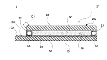
図1及び図2を参照しながら、本実施形態に係る液晶装置の構成を説明する。図1は、本実施形態に係る液晶装置を対向基板側から見た平面図であり、図2は、図1のII−II´断面図である。図3は、図2に一部を部分的に拡大して示した部分拡大図である。
<First Embodiment>
<1: Electro-optical device>
The configuration of the liquid crystal device according to the present embodiment will be described with reference to FIGS. 1 and 2. FIG. 1 is a plan view of the liquid crystal device according to the present embodiment as viewed from the counter substrate side, and FIG. 2 is a cross-sectional view taken along the line II-II ′ of FIG. FIG. 3 is a partial enlarged view showing a part of FIG. 2 partially enlarged.
図1及び図2において、液晶装置1では、本発明の「素子基板」の一例であるTFTアレイ基板10と、対向基板20とが対向配置されている。TFTアレイ基板10と対向基板20との間に、本発明の「電気光学層」の一例である液晶層50が封入されており、TFTアレイ基板10と対向基板20とは、画像表示領域10aの周囲に位置するシール領域に設けられたシール材52により相互に接着されている。液晶層50は、その駆動時に応じて画像のコントラスト及び液晶装置1の透過率が可変となるように構成されている。
1 and 2, in the
シール材52は、両基板を貼り合わせるための、例えば紫外線硬化樹脂、熱硬化樹脂等からなり、液晶装置1の製造プロセスにおいてTFTアレイ基板10上に塗布された後、紫外線照射、加熱等により硬化させられたものである。シール材52中には、TFTアレイ基板10と対向基板20との間隔(基板間ギャップ)を所定値とするためのグラスファイバ或いはガラスビーズ等のギャップ材56が散布されている。
The sealing
シール材52が配置されたシール領域の内側に並行して、画像表示領域10aの額縁領域を規定する遮光性の額縁遮光膜53が、対向基板20側に設けられている。但し、このような額縁遮光膜53の一部又は全部は、対向基板20上において、電極より上層側に配置されて形成されてもよいし、TFTアレイ基板10側に内蔵遮光膜として形成されてもよい。
A light-shielding frame light-shielding
画像表示領域10aの周辺に位置する周辺領域のうち、シール材52が配置されたシール領域の外側に位置する領域には、データ線駆動回路101、及び接続端子としての外部回路接続端子102がTFTアレイ基板10の一辺に沿って複数設けられている。液晶装置1を駆動させるための電源及び各種信号は、外部回路に電気的に接続された外部回路端子102を介して液晶装置1に供給される。これにより液晶装置1が動作状態となる。
In the peripheral region located around the
走査線駆動回路104は、この一辺に隣接する2辺のいずれかに沿い、且つ、額縁遮光膜53に覆われるようにして設けられている。尚、走査線駆動回路104を、データ線駆動回路101及び外部回路接続端子102が設けられたTFTアレイ基板10の一辺に隣接する2辺に沿って設けるようにしてもよい。この場合、TFTアレイ基板10の残る一辺に沿って設けられた複数の配線によって、二つの走査線駆動回路104は互いに接続されるようにする。
The scanning
対向基板20の4つのコーナー部には、両基板間の上下導通端子として機能する上下導通材106が配置されている。他方、TFTアレイ基板10にはこれらのコーナー部に対向する領域において上下導通端子が設けられている。これらにより、TFTアレイ基板10と対向基板20との間で電気的な導通をとることができる。
Vertical
図2において、TFTアレイ基板10上には、画素スイッチング用のスイッチング素子としてのTFT(Thin Film Transistor;以下適宜、“TFT”と称する。)や走査線、データ線等の配線が形成された後の画素電極9a上に、配向膜16が形成されている。他方、詳細な構成については省略するが、液晶装置1において、対向基板20に形成された電極が、画素電極9aと対向するように配置されており、その上に配向膜22が形成されている。尚、TFTアレイ基板10及び対向基板20には、液晶装置1の表示方式、より具体的には、透過型表示方式或いは反射型表示方式の違いに応じて、ガラス基板、石英、プラスチック基板、或いはシリコン基板等の各種基板が用いられる。
In FIG. 2, after a TFT (Thin Film Transistor; hereinafter referred to as “TFT” as appropriate), a scanning line, a data line, and the like are formed on the
次に、図3を参照しながら、TFTアレイ基板10の縁の形状を詳細に説明する。図3は、図2中の範囲C1を拡大して示した拡大図である。
Next, the shape of the edge of the
図3において、対向基板20の両面のうち液晶層50に面しない側の面20Sを規定する複数の縁の少なくとも一つの縁である縁27は、面取り部27aを有している。したがって、対向基板20の端面が切り立った面である場合に比べて、例えば、液晶装置1の搬送時において発生する可能性があるクラックを低減でき、液晶装置1の外形が損傷を受けることを低減できる。加えて、クラックの発生が低減できるため、走査線駆動回路104、データ線駆動回路101及び外部回路接続端子102を相互に電気的に接続する配線が受ける損傷も低減でき、液晶装置1が画像を表示する際の表示性能が低下することを抑制できる。
In FIG. 3, the
尚、本実施形態に係る液晶装置1では、縁27だけでなく、TFTアレイ基板10及び対向基板20の夫々における他の縁も面取り部を有していてもよい。面取り部が多く設けられていることによって、TFTアレイ基板10及び対向基板20の夫々におけるクラックの発生を効果的に低減でき、液晶装置1の外形精度を面取り部が設けられていない場合に比べて高めることができると共に、その表示性能も向上させることが可能である。
In the
<2:電気光学装置の製造方法>
次に、図4乃至図10を参照しながら、本実施形態に係る電気光学装置の製造方法を説明する。図4は、本実施形態に係る電気光学装置の製造方法に用いられる複合基板を図式的に示した平面図である。図5は、図4の一部を拡大して示した拡大平面図である。図6乃至図8の夫々は、本実施形態に係る電気光学装置の製造方法の主要な工程を順に示した工程断面図である。図9は、図6(a)に示した切り込み工程に対応する工程平面図であり、図10は、図7及び図8において対応する各工程の工程平面図である。
<2: Manufacturing method of electro-optical device>
Next, a method for manufacturing the electro-optical device according to the present embodiment will be described with reference to FIGS. FIG. 4 is a plan view schematically showing a composite substrate used in the method for manufacturing an electro-optical device according to this embodiment. FIG. 5 is an enlarged plan view showing a part of FIG. 4 in an enlarged manner. 6 to 8 are process cross-sectional views sequentially showing main processes of the method of manufacturing the electro-optical device according to this embodiment. 9 is a process plan view corresponding to the cutting process shown in FIG. 6A, and FIG. 10 is a process plan view of each process corresponding to FIG. 7 and FIG.
尚、以下で説明する電気光学装置の製造方法は、上述の液晶装置1を製造する製造方法である。以下では、説明の便宜上、上述の液晶装置1と共通する部分に共通の参照符号を付し、詳細な説明を省略する。加えて、液晶装置1を構成する構成要素であるシール材52及び液晶層50の図示を省略する。
The electro-optical device manufacturing method described below is a manufacturing method for manufacturing the
図4に示すように、複合基板230は、第1基板210と、第1基板210に対向するように第1基板210に貼り合わせられた第2基板220とを有している。第1基板210及び第2基板220は、最終的に製造される液晶装置1のサイズより大きい大型の基板である。第1基板210及び第2基板220は、シール材等の接着剤から構成されるシール部を介して相互に貼り合わせられている。第1基板210上で図中X方向及びY方向に延び、且つ相互に交差する複数の第1外形線250X及び複数の第2外形線250Yによって囲まれた第1基板210上の複数の領域rの夫々における画像表示領域10aとなるべき領域において、液晶層50(図2参照)は第1基板210及び第2基板220間に封止されている。第1外形線250X及び第2外形線250Yは、第1基板210及び第2基板220、並びに、これら基板間に封止される液晶層50を含んで構成される複合基板230のうち最終的に複数の液晶装置1となるべき部分、即ち、第1基板210上において液晶装置1となるべき複数の領域rを規定するために製造プロセス上便宜的に設定される仮想的な線である。
As shown in FIG. 4, the
複数の領域rのうち第1基板210及び第2基板220を相互に接着するシール材によって囲まれた領域が、最終的に製造される液晶装置1の画像表示領域10aになる領域を含んでいる。液晶層50は、第1基板210及び第2基板220が相互に貼り合わせられる前に、各々がシール材によって囲まれた複数の領域rに塗布された状態で、複合基板230のうち複数の液晶装置1となるべき部分の一部を構成するように封止されている。
Of the plurality of regions r, a region surrounded by a sealing material that bonds the
したがって、本実施形態に係る電気光学装置の製造方法は、ODF法によって形成された複合基板230、即ち最終的に製造される液晶装置1のサイズより大型の複合基板230から、後述各工程を経て複数の液晶装置1を製造する。
Therefore, the electro-optical device manufacturing method according to the present embodiment is performed from the
次に、図5を参照しながら、図4中の領域Rにおける複合基板230の詳細な構成を説明する。尚、図5では、第1基板210及び第2基板220が相互に重なっているため、これら基板を区別可能なように図示していない。
Next, a detailed configuration of the
図5に示すように、領域Rでは、第1基板210の複数の領域rの夫々には、外部回路接続用端子102が形成されていると共に、シール材52に囲まれた領域に画像表示領域10aが設定されている。このような画像表示領域10aは、液晶装置1において遮光膜53(図1参照)等の遮光部によってその外縁が規定される。第1基板210のうち第1外形線250X及び第2外形線250Yで規定された領域r(斜線で図示)に重なる部分が、液晶装置1におけるTFTアレイ基板10に相当する。
As shown in FIG. 5, in the region R, the external
次に、図6乃至図10を参照しながら、本実施形態に係る電気光学装置の製造方法を詳細に説明する。 Next, the method for manufacturing the electro-optical device according to the present embodiment will be described in detail with reference to FIGS.
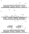
図6(a)及び図9に示すように、第2基板220の両面のうち液晶層50に面しない側の切り込み面220aから、第1外形線250Xに沿って第1切り込み部221を形成する(第1工程)。したがって、第1切り込み部221は、切り込み面220aにおいて、第1外形線250Xに沿って不連続に、或いは部分的に形成されるのではなく、第1外形線250Xに沿って連続的に延びるように形成される。より具体的には、第1切り込み部221は、シール材52の複数の縁のうちY方向に沿って外部回路接続用端子102に近い側でX方向に延びる縁の近い位置に形成される。第1切り込み部221は、液晶装置1が完成した際には、面取り部27aとなる。よって、対向基板20における切り立った端面に起因して生じるクラックを低減することが可能である。
As shown in FIGS. 6A and 9, the
次に、図6(b)に示すように、第1基板210の両面のうち液晶層50に面しない貼り付け面210aに第1テープ261を貼り付ける(第2工程)。第1テープ261は、後述する第3工程において複合基板230をブレイクすることを目的として貼り付けられているため、貼り付け面210a全体に貼り付けられる。尚、第1テープ261には、後述する第3工程を安定して実行するために、平面的に見て複合基板230を囲むようにリング270が配置されている。
Next, as illustrated in FIG. 6B, the
本実施形態では、第1工程及び第2工程の間において、CO2等のガス又はドライアイスを用いて複合基板230を洗浄する。したがって、第1切り込み部221を形成する際に生じたガラス等のくずを除去することができる。よって、後の工程で第1切り込み部221を形成する際に生じた削りくずが外部接続用端子102に付着する低減でき、当該端子部を外部回路に接続した際に生じる可能性がある電気的な接触不良を低減できる。
In the present embodiment, the
次に、図6(c)に示すように、第1テープ261の両面のうち貼り付け面210aに接しない裏面261aの側から第1切り込み部221に向かって力F1を加えることによって、第1切り込み部221を起点として、第2基板220の両面のうち液晶層50に面する側の第1面220bまで延びる第1分離面222を形成する(第3工程)。即ち、第3工程によれば、第1外形線250Xに沿って延びる第1分離面222によって、第2基板220は、第2外形線250Yに沿って相互に分離されるようにブレイクされる。
Next, as shown in FIG. 6C, by applying a force F1 from the back surface 261a side that does not contact the
次に、図7(d)及び図10に示すように、切り込み面220aにおいて、第1外形線250Xに沿って、且つ前記第1分離面222とずれた位置から第2基板220にダイシング処理を施すことによって、切り込み面220aから第1面220bまで延びる第1分離溝223を形成する(第4工程)。第1分離溝223は、第1基板210の両面のうち液晶層50に面する側の面を規定する複数の縁のうち外部回路接続用端子102が形成されている側の縁に沿って当該縁に重なるように形成される。このように外部回路接続用端子102上では、ダイシング処理のみを行なうので、外部回路接続用端子102及び外部回路接続用端子102に電気的に接続された配線を傷付けることが無い。また、第1切り込み部221に沿ってハーフダイシング処理を行なうことにより対向基板20の外形寸法精度を向上させる。この際に、対向基板20の面取り部27aが形成される。
Next, as shown in FIGS. 7D and 10, the dicing process is performed on the
これと並行して、或いは相前後して、第4工程では、第2外形線250Yに沿って切り込み面220aから第2基板220にダイシング処理を施すことによって、第2外形線250Yに沿って延びる第2分離溝224を第2基板220に形成する。即ち、第2分離溝224は、第1分離溝223とは相互に交差するように延びており、第1外形線250Xが延びる方向に沿って第2基板220を複数の部分、即ち複数の液晶装置1の夫々に対応する部分に相互に分離する際の起点となる。このような第2分離溝224は、第2基板220の厚み方向に沿って当該基板の途中まで延びていてもよいし、第1面220bまでに延びるように形成されてもよい。
In parallel with or in parallel with this, in the fourth step, the
次に、図7(e)及び図10に示すよう、第2基板220のうち第1分離面222、第1分離溝223、及び第1面220bに囲まれた部分である小片部225を除去する(第5工程)。小片部225は、最終的に製造される液晶装置1において、外部回路接続用端子102と重なる部分であるため、当該工程で予め除去しておく。
Next, as shown in FIGS. 7E and 10, the
本実施形態では、第4工程及び第5工程間において、複合基板230を乾燥させ、ダイシング処理の際に複合基板230に供給された切削水を蒸発させ、最終的に製造される液晶装置1に残留する切削水の残留量を低減する。
In the present embodiment, between the fourth step and the fifth step, the
次に、図7(f)に示すように、第1テープ261を貼り付け面210aから取り除いた後、切り込み面220aに第2テープ262を貼り付ける(第6工程)。これにより、切り込み面220a側から複合基板230が第2テープ262に固定される。尚、第2テープ262は、第1テープ261と同様に、切り込み面220aの全体、より具体的には、上述の小片部225が除去された後の切り込み面220a全体に貼り付けられているほうが好ましい。
Next, as shown in FIG. 7F, after the
次に、図8(g)及び図10に示すように、貼り付け面210aにおける第1分離溝223に対応した位置に第1外形線250Xに沿って第2切り込み部211を形成する(第7工程)。これにより、第1基板210を第2外形線250Yに沿って液晶装置1に対応する部分毎に分離する準備が整う。
Next, as shown in FIG. 8G and FIG. 10, the
次に、図8(h)及び図10に示すように、第2テープ262の両面のうち貼り付け面220aに面しない裏面262aの側から第2切り込み部211に向かって力F2を加えることによって、第2切り込み部211を起点として、第1基板210の両面のうち液晶層50に面する側の第2面210bまで延びる第2分離面212を形成すると共に、2分離溝224を起点として、第2外形線250Yに沿って延びる第3分離面213を形成する(第8工程)。第2切り込み部211は、第1基板210をブレイクする際の起点となる切り込み部である。したがって、第2テープ262の両面のうち貼り付け面210aに面しない裏面262aの側から第2切り込み部211に向かって力F2を加えることによって、第1基板210がブレイクされる。これと並行して、或いは相前後して、第2分離溝224を起点として、第2外形線250Yに沿って第3分離面213が形成される。このような第3分離面213は、第1外形線250Xに沿って複数の液晶装置1を相互に分離し、液晶装置1が完成した際には、液晶装置1を構成する基板部分の端面となる。
Next, as shown in FIG. 8 (h) and FIG. 10, by applying a force F2 from the
尚、上述の第2切り込み部211も第1切り込み部221と同様に面取り部となるため、クラックの発生を低減できる利点がある。
In addition, since the above-mentioned
次に、図8(i)に示すように、第8工程によって相互に分離された複数の液晶装置1を第2テープ262から分離する(第9工程)。複数の液晶装置1を第2テープ262から取り除く際、言い換えれば、第2テープ262からはがす際には、ソータ装置等の吸引手段によって複数の液晶装置1を吸引する。
Next, as shown in FIG. 8I, the plurality of
尚、本実施形態に係る電気光学装置の製造方法によれば、前記第8工程の後、CO2等のガスを用いて複合基板230を洗浄し、第2切り込み部211を形成する際に生じた削りくずを除去することができる。したがって、削りくずが外部回路接続用端子102に付着することによって発生する電気的な接触不良を低減できる。
In addition, according to the method of manufacturing the electro-optical device according to the present embodiment, after the eighth step, the
以上説明したように、本実施形態に係る電気光学装置の製造方法によれば、第1外形線250X及び第2外形線250Yに沿って、複合基板230から複数の液晶装置1が相互に分離されるため、外形精度が高い液晶装置1を製造可能である。加えて、第1切り込み部221及び第2切り込み部211が、液晶装置1の基板部分の縁における面取り部となるため、例えば、液晶装置1の搬送時に基板部分の縁に加わる衝撃に起因してクラックが発生することを低減でき、液晶装置1の外形精度を高めることができることに加えて、クラックの発生に起因して配線が損傷を受けることを低減できる。したがって、液晶装置1が画像を表示する際の表示性能が低下することを抑制することも可能である。
As described above, according to the method of manufacturing the electro-optical device according to the present embodiment, the plurality of
<3:電子機器>
次に、上述した液晶装置を用いた電子機器の一例を説明する。本実施形態に係る電子機器は、上述した液晶装置をライトバルブに用い、当該ライトバルブの光入射側及び光出射側の夫々の側に位相差板を配置した光学系を有するプロジェクタである。図11は、本実施形態に係るプロジェクタの構成例を示す平面図である。
<3: Electronic equipment>
Next, an example of an electronic device using the above-described liquid crystal device will be described. The electronic apparatus according to the present embodiment is a projector having an optical system in which the liquid crystal device described above is used for a light valve, and a retardation plate is disposed on each of the light incident side and the light emission side of the light valve. FIG. 11 is a plan view showing a configuration example of the projector according to the present embodiment.
図11に示すように、プロジェクタ1100内部には、ハロゲンランプ等の白色光源からなるランプユニット1102が設けられている。このランプユニット1102から射出された投射光は、ライトガイド1104内に配置された4枚のミラー1106および2枚のダイクロイックミラー1108によってRGBの3原色に分離され、各原色に対応するライトバルブとしての液晶パネル1110R、1110Bおよび1110Gに入射される。
As shown in FIG. 11, a
液晶パネル1110R、1110Bおよび1110Gの構成は、上述した液晶装置と同等であり、画像信号処理回路から供給されるR、G、Bの原色信号でそれぞれ駆動されるものである。そして、これらの液晶パネルに入射する光或いは出射される光は上述の位相差膜によって光学補償されている。液晶パネル及び位相差板を含む光学系から出射された光は、ダイクロイックプリズム1112に3方向から入射される。このダイクロイックプリズム1112においては、RおよびBの光が90度に屈折する一方、Gの光が直進する。したがって、各色の画像が合成される結果、投射レンズ1114を介して、スクリーン等にカラー画像が投写されることとなる。
The configurations of the
ここで、各液晶パネル1110R、1110Bおよび1110Gによる表示像について着目すると、液晶パネル1110Gによる表示像は、液晶パネル1110R、1110Bによる表示像に対して左右反転することが必要となる。
Here, paying attention to the display images by the
尚、液晶パネル1110R、1110Bおよび1110Gには、ダイクロイックミラー1108によって、R、G、Bの各原色に対応する光が入射するので、カラーフィルタを設ける必要はない。
Since light corresponding to the primary colors R, G, and B is incident on the
尚、本実施形態に係る液晶装置は、上述した投写型表示装置に適用される場合に限定されるものではなく、直視型の液晶表示装置の一部を構成することも可能である。また、LCOS等の反射型の液晶装置を構成することも可能である。 Note that the liquid crystal device according to the present embodiment is not limited to the case where it is applied to the projection display device described above, and may constitute a part of a direct-view type liquid crystal display device. It is also possible to configure a reflective liquid crystal device such as LCOS.
<第2実施形態>
第2実施形態に係る電気光学装置の製造方法について、図12から図15を参照して説明する。尚、第2実施形態に係る電気光学装置の製造方法は、本発明に係る第2の電気光学装置の製造方法の一例である。また、図12から図15において、図1から図10に示した第1実施形態に係る構成要素と同様の構成要素に同一の参照符合を付し、それらの説明は適宜省略する。
Second Embodiment
A method for manufacturing the electro-optical device according to the second embodiment will be described with reference to FIGS. The electro-optical device manufacturing method according to the second embodiment is an example of the second electro-optical device manufacturing method according to the present invention. 12 to 15, the same reference numerals are given to the same components as the components according to the first embodiment illustrated in FIGS. 1 to 10, and description thereof will be omitted as appropriate.
図12から図14の夫々は、第2実施形態に係る電気光学装置の製造方法の主要な工程を順に示した工程断面図である。図15は、第2実施形態に係る電気光学装置の製造方法に用いられる複合基板の一部を拡大して示した拡大平面図である。 12 to 14 are process cross-sectional views sequentially showing main processes of the method for manufacturing the electro-optical device according to the second embodiment. FIG. 15 is an enlarged plan view illustrating a part of the composite substrate used in the method for manufacturing the electro-optical device according to the second embodiment.
図15において、第2実施形態に係る電気光学装置の製造方法は、ODF法によって形成された複合基板230を、後述する各工程によって複数の第1外形線250X及び複数の第2外形線250Y並びに切断予定線900に沿って切断することにより、複数の液晶装置1を製造する。
In FIG. 15, the method for manufacturing the electro-optical device according to the second embodiment uses a
図12(a)及び図15に示すように、先ず、第2基板220の両面のうち液晶層50に面しない側の切り込み面220aに、切断予定線900に沿ってスクライブ処理を施すことによりスクライブ溝1221を形成する(第1工程)。スクライブ溝1221は、切断予定線900に沿って連続的に延びるように形成される。尚、切り込み面220aは、本発明に係る第2の電気光学装置の製造方法における「第2基板外面」の一例である。
As shown in FIG. 12A and FIG. 15, first, scribing is performed on the
ここで図15に示すように、切断予定線900は、第1外形線250X及び第2外形線250Yと同様に製造プロセス上便宜的に設定される仮想的な線である。切断予定線900は、第1外形線250Xに対して第1基板210上における外部回路接続端子102が形成される領域102aを隔てて且つ第1外形線250Xに沿って規定されている。スクライブ処理は、例えばダイヤモンドチップなどのカッタを切り込み面220aに当接させたまま、このカッタを切断予定線900に沿って相対移動させることにより行う。
Here, as shown in FIG. 15, the
次に、図12(b)に示すように、第1基板210の両面のうち液晶層50に面しない側の貼り付け面210aに、第1テープ261を貼り付ける(第2工程)。尚、貼り付け面210aは、本発明に係る第2の電気光学装置の製造方法における「第1基板外面」の一例である。第1テープ261は、後述する第3工程において第2基板220にブレイク処理を施すことを目的として貼り付けられているため、貼り付け面210aに貼り付けられる。尚、第1テープ261には、後述する第3工程を安定して実行するために、平面的に見て複合基板230を囲むようにリング270が配置されている。
Next, as shown in FIG. 12B, the
次に、図12(c)及び図15に示すように、第1テープ261の両面のうち第1基板210に面しない側の裏面261aから第1テープ261及び第1基板210を介して第2基板220を押圧する(即ち、第2基板220に対して力F1を加える)ことにより、スクライブ溝1221を起点として、第2基板210にブレイク処理を施す(第3工程)。尚、裏面261aは、本発明に係る第2の電気光学装置の製造方法における「第1テープ外面」の一例である。第3工程によれば、スクライブ溝1221を起点とするクラック1222によって、第2基板220が相互に分断される。ここで、スクライブ溝1221は、切断予定線900に沿って形成されているので、第2基板220は、切断予定線900に沿ってブレイクされる。
Next, as shown in FIG. 12C and FIG. 15, the second surface 261 a on the side of the
次に、図13(d)及び図15に示すように、第2基板220に対して、切り込み面220a側から、(i)切断予定線900に沿って(即ち、スクライブ溝1221及びクラック1222に重ねて)所定の深さd1までダイシング処理を施すことによりダイシング溝1224を形成すると共に、(ii)第1外形線250Xに沿って、ダイシング処理を、第2基板220を貫通して、第1基板210の両面のうち液晶層50に面する側の第1面210bに切り込み部(或いは切溝)1223vが形成されるように、施すことにより第2基板220を第1外形線250Xに沿って切断する(第4工程)。尚、第1面210bは、本発明に係る第2の電気光学装置の製造方法における「第1基板内面」の一例である。
Next, as shown in FIG. 13D and FIG. 15, (i) along the planned cutting line 900 (i.e., to the
即ち、第4工程では、第2基板220に対して、切り込み面220a側から、切断予定線900及び第1外形線250Xに沿ってダイシング処理を施すが、切断予定線900に沿ってダイシング処理を施す際には、第2基板220を完全には切断しないように、ダイシング処理を、第2基板220の厚さよりも小さい所定の深さd1まで施すことによりダイシング溝1224を形成し、第1外形線250Xに沿ってダイシング処理を施す際には、第2基板220を完全に切断すると共に第1面210bに切り込み部1223vを形成するように、ダイシング処理を施す。ここで、ダイシング処理は、高速回転させた例えばダイヤモンド製等の円形回転刃(即ち、ダイシングブレード)を、切り込み面220a側から押し当てることにより行う。
That is, in the fourth step, dicing processing is performed on the
よって、第4工程によって、第2基板220における切断予定線900に沿った切断面を、ダイシング溝1224の側面1224aによって規定される部分を含むように形成できる。即ち、第2基板220における切断予定線900に沿った切断面のうち、切り込み面220aから所定の深さd1までの部分を、ダイシング溝1224の側面1224aによって規定されるように、第2基板220を切断することができる。このようなダイシング溝1224の側面1224aによって規定される切断面は、例えばスクライブ溝1221を起点とするクラック1222により規定される切断面と比較して、平滑性が高く、所望の切断面を高精度に形成できる。また、第4工程では、第2基板220における第1外形線250Xに沿った切断面を、ダイシング処理によって形成するので、第2基板220における第1外形線250Xに沿った切断面を、平滑性の高い所望の切断面として高精度に形成できる。従って、第2基板220における第1外形線250Xに沿った切断面や、切断予定線900に沿った切断面のうちダイシング溝1224の側面1224aによって規定される部分を、例えば、液晶装置1を実装ケースに収容する際の位置決め手段として好適に用いることができる。つまり、液晶装置1を実装ケースに収容する際、第2基板220における第1外形線250Xに沿った切断面や、切断予定線900に沿った切断面のうちダイシング溝1224の側面1224aによって規定される部分を位置決め手段として用いることで、実装ケース内における液晶装置1の位置ずれの発生を殆ど或いは完全に無くすことができる、或いは、実装ケース内に液晶装置1を収容できなくなる事態を回避できる。
Therefore, by the fourth step, the cut surface along the
更に、第4工程では、切断予定線900に沿ってダイシング処理を施す際には、第2基板220を完全には切断しないように、ダイシング処理を、第2基板220の厚さよりも小さい所定の深さd1まで施すので、後述する第5工程において、第2基板220に対してダイシング処理を施すことにより、第2基板220を第2外形線250Yに沿って切断する際、第2基板220のうち第1外形線250X及び切断予定線900によって挟まれる小片部分1225(即ち、第2基板210のうち領域102aに位置する部分)が、周辺に飛び散ってしまう或いは散乱してしまうことを防止できる。
Further, in the fourth step, when the dicing process is performed along the
加えて、第4工程によって、第1基板210の第1面210bに第1外形線250Xに沿って切り込み部1223vが形成されるので、後述する第9工程において、第1基板210に第1外形線250Xに沿ってブレイク処理を施した際の切断面の面精度を高めることができる。また、切り込み部1223vにより後述する第11工程後のTFTアレイ基板10の対向基板20側との対向面側の縁部は同時に面取りされる。これにより、液晶装置1の外形精度が向上する。
In addition, since the
次に、第2基板220に対して、切り込み面220a側から、第2外形線250Yに沿ってダイシング処理を施すことにより、第2基板220を第2外形線250Yに沿って切断する(第5工程)。よって、第2基板220における第2外形線250Yに沿った切断面を、平滑性の高い所望の切断面として高精度に形成できる。
Next, the
次に、図13(e)及び図15に示すように、第2基板220のうち、第2基板220上で平面的に見て第1外形線250X及び切断予定線900によって挟まれる、領域102aに位置する小片部分1225を除去する(第6工程)。小片部分1225は、最終的に製造される液晶装置1において、外部回路接続端子102と重なる部分であるため、当該工程で予め除去しておく。
Next, as shown in FIGS. 13E and 15, the
次に、図13(f)に示すように、第1テープ261を貼り付け面210aから取り除いた後、切り込み面220aに第2テープ262を貼り付ける(第7工程)。これにより、切り込み面220a側から複合基板230が第2テープ262に固定される。尚、第2テープ262は、第1テープ261と同様に、切り込み面220aの全体、より具体的には、上述した小片部分1225が除去された後の切り込み面220a全体に貼り付けられる。
Next, as shown in FIG. 13F, after the
次に、図14(g)及び図15に示すように、第1基板210の貼り付け面210aに、第1外形線250Xに沿ってスクライブ処理を施すことにより、スクライブ溝1226を形成すると共に、第2外形線250Yに沿ってスクライブ処理を施すことにより、スクライブ溝(図示省略)を形成する(第8工程)。これにより、第1基板210を第1外形線250X及び第2外形線250Yに沿って液晶装置1に対応する部分毎に分離する準備が整う。
Next, as shown in FIG. 14G and FIG. 15, a
次に、図14(h)及び図15に示すように、第2テープ262の両面のうち第2基板220に面しない側の裏面262aから第2テープ262及び第2基板220を介して第1基板210を押圧する(即ち、第1基板210に対して力F2を加える)ことにより、スクライブ溝1226を起点として切り込み部1223vまで延びる切断面1227を形成して、第1基板210に第1外形線250Xに沿ってブレイク処理を施す(第9工程)。尚、裏面262aは、本発明に係る第2の電気光学装置の製造方法における「第2テープ外面」の一例である。ここで、第9工程において、第1基板210に第1外形線250Xに沿ってブレイク処理を施す際には、上述したように、第4工程によって、第1基板210の第1面210bに第1外形線250Xに沿って切り込み部1223vが形成されているので、第1基板210に第1外形線250Xに沿ってブレイク処理を施した際の切断面1227の面精度を高めることができる。
Next, as shown in FIG. 14H and FIG. 15, the first surface of the
次に、第2テープ262の裏面262aから第2テープ262及び第2基板220を介して第1基板210を押圧することにより、上述した第8工程によって第2外形線250Yに沿って形成されたスクライブ溝を起点として、第1基板210に第2外形線250Yに沿ってブレイク処理を施す(第10工程)。尚、第9工程及び第10工程は、いずれが先に行われてもよい。
Next, by pressing the
次に、図14(i)に示すように、上述した第1工程から第10工程までの一連の工程によって相互に分離された複数の液晶装置1を第2テープ262から分離する(第11工程)。複数の液晶装置1を第2テープ262から取り除く際、言い換えれば、第2テープ262からはがす際には、ソータ装置等の吸引手段によって複数の液晶装置1を吸引する。
Next, as shown in FIG. 14 (i), the plurality of
以上説明したように、本実施形態に係る電気光学装置の製造方法によれば、外形精度が高い液晶装置1を製造することができる。よって、歩留りを向上させることも可能である。
As described above, according to the method of manufacturing the electro-optical device according to the present embodiment, the
1・・・液晶装置、10・・・TFTアレイ基板、20・・・対向基板、50・・・液晶層、210・・・第1基板、220・・・第2基板、230・・・複合基板
DESCRIPTION OF
Claims (4)
前記第2基板の前記電気光学層とは反対側の切り込み面から、前記第1外形線に沿って第1切り込み部を形成する第1工程と、
前記第1基板の前記電気光学層とは反対側の貼り付け面に第1テープを貼り付ける第2工程と、
前記第1テープの前記貼り付け面と反対側の面から前記第1切り込み部に向かって力を加えることによって、前記第1切り込み部を起点として、前記第2基板の前記電気光学層側の第1面まで延びる第1分離面を形成する第3工程と、
前記切り込み面において、前記第1外形線に沿って、且つ前記第1分離面とは異なる位置から前記第2基板にダイシング処理を施すことによって、前記切り込み面から前記第1面まで延びる第1分離溝を形成すると共に、前記第2外形線に沿って前記切り込み面から前記第2基板にダイシング処理を施すことによって、前記第2外形線に沿って延びる第2分離溝を前記第2基板に形成する第4工程と、
前記第2基板のうち前記第1分離面、前記第1分離溝、前記第2分離溝及び前記第1面に囲まれた部分を除去する第5工程と、
前記第1テープを前記貼り付け面から取り除いた後、前記切り込み面に第2テープを貼り付ける第6工程と、
前記第2テープが貼り付けられた面と反対側の面に、前記第1及び第2外形線に沿って第2及び第3切り込み部をそれぞれ形成する第7工程と、
前記第2テープの前記貼り付け面と反対側の面から前記第2切り込み部に向かって力を加えることによって、前記第2切り込み部を起点として、前記第1基板の前記電気光学層側の第2面まで延びる第2分離面を形成すると共に、前記第3切り込み部を起点として、前記第2外形線に沿って延びる前記第3分離面を形成する第8工程と、
前記第8工程によって相互に分離された前記複数の電気光学装置を前記第2テープから分離する第9工程と
を備えたことを特徴とする電気光学装置の製造方法。 A composite substrate in which a first substrate and a second substrate facing the first substrate via an electro-optic layer are bonded to each other by a plurality of first outlines and a plurality of second outlines that intersect each other. An electro-optical device manufacturing method for cutting and manufacturing a plurality of electro-optical devices,
A first step of forming a first cut portion along the first outline from a cut surface of the second substrate opposite to the electro-optic layer;
A second step of affixing a first tape to a surface of the first substrate opposite to the electro-optic layer;
By applying a force from the surface of the first tape on the side opposite to the attachment surface toward the first cut portion, the first cut portion as a starting point, the second substrate on the electro-optic layer side A third step of forming a first separation surface extending to one surface;
A first separation extending from the cut surface to the first surface by dicing the second substrate from a position different from the first separation surface along the first outline on the cut surface. A groove is formed, and a second separation groove extending along the second outline is formed in the second substrate by subjecting the second substrate to dicing from the cut surface along the second outline. And a fourth step to
A fifth step of removing a portion surrounded by the first separation surface, the first separation groove , the second separation groove, and the first surface of the second substrate;
A sixth step of attaching the second tape to the cut surface after removing the first tape from the application surface;
A seventh step of forming second and third cut portions along the first and second outlines on the surface opposite to the surface to which the second tape is attached ,
By applying a force from the surface opposite to the attachment surface of the second tape toward the second cut portion, the second cut portion is used as a starting point and the second substrate on the electro-optic layer side of the first substrate is used. An eighth step of forming a second separation surface extending to two surfaces, and forming the third separation surface extending along the second outline from the third cut portion as a starting point;
And a ninth step of separating the plurality of electro-optical devices separated from each other in the eighth step from the second tape.
を特徴とする請求項1に記載の電気光学装置の製造方法。 The method of manufacturing an electro-optical device according to claim 1, wherein the composite substrate is cleaned with a gas after the first step.
を特徴とする請求項1又は2に記載の電気光学装置の製造方法。 The method of manufacturing an electro-optical device according to claim 1, wherein the composite substrate is dried after the fourth step.
を特徴とする請求項1から3の何れか一項に記載の電気光学装置の製造方法。 4. The method of manufacturing an electro-optical device according to claim 1, wherein the composite substrate is cleaned with a gas after the eighth step. 5.
Priority Applications (2)
| Application Number | Priority Date | Filing Date | Title |
|---|---|---|---|
| JP2008332755A JP5304232B2 (en) | 2008-02-01 | 2008-12-26 | Manufacturing method of electro-optical device |
| US12/362,216 US7741137B2 (en) | 2008-02-01 | 2009-01-29 | Method of manufacturing electro-optical device |
Applications Claiming Priority (3)
| Application Number | Priority Date | Filing Date | Title |
|---|---|---|---|
| JP2008022422 | 2008-02-01 | ||
| JP2008022422 | 2008-02-01 | ||
| JP2008332755A JP5304232B2 (en) | 2008-02-01 | 2008-12-26 | Manufacturing method of electro-optical device |
Publications (3)
| Publication Number | Publication Date |
|---|---|
| JP2009205140A JP2009205140A (en) | 2009-09-10 |
| JP2009205140A5 JP2009205140A5 (en) | 2012-01-19 |
| JP5304232B2 true JP5304232B2 (en) | 2013-10-02 |
Family
ID=40930681
Family Applications (1)
| Application Number | Title | Priority Date | Filing Date |
|---|---|---|---|
| JP2008332755A Expired - Fee Related JP5304232B2 (en) | 2008-02-01 | 2008-12-26 | Manufacturing method of electro-optical device |
Country Status (2)
| Country | Link |
|---|---|
| US (1) | US7741137B2 (en) |
| JP (1) | JP5304232B2 (en) |
Cited By (1)
| Publication number | Priority date | Publication date | Assignee | Title |
|---|---|---|---|---|
| KR20190066752A (en) * | 2017-12-06 | 2019-06-14 | 주식회사 제우스 | Display separating method and display separating apparatus |
Families Citing this family (5)
| Publication number | Priority date | Publication date | Assignee | Title |
|---|---|---|---|---|
| US20130168147A1 (en) * | 2010-10-08 | 2013-07-04 | Yasuhiro Kohara | Electronic device |
| US8558247B2 (en) * | 2011-09-06 | 2013-10-15 | Toshiba Techno Center Inc. | GaN LEDs with improved area and method for making the same |
| US9894781B2 (en) * | 2012-06-06 | 2018-02-13 | Apple Inc. | Notched display layers |
| KR102439023B1 (en) | 2014-10-28 | 2022-08-31 | 가부시키가이샤 한도오따이 에네루기 켄큐쇼 | Display device, manufacturing method of display device, and electronic device |
| JP7127566B2 (en) * | 2019-02-07 | 2022-08-30 | 株式会社Jvcケンウッド | Liquid crystal device manufacturing method |
Family Cites Families (8)
| Publication number | Priority date | Publication date | Assignee | Title |
|---|---|---|---|---|
| JP3042192B2 (en) | 1992-07-29 | 2000-05-15 | 三星ダイヤモンド工業株式会社 | Method and apparatus for cutting laminated glass substrate |
| JP3528216B2 (en) * | 1993-10-26 | 2004-05-17 | カシオ計算機株式会社 | Glass cutting method |
| JP4502964B2 (en) | 2001-04-02 | 2010-07-14 | 三星ダイヤモンド工業株式会社 | Method for dividing bonded substrates |
| JPWO2003040049A1 (en) | 2001-11-08 | 2005-03-03 | シャープ株式会社 | Glass substrate cutting method, glass substrate cutting device, liquid crystal panel, and liquid crystal panel manufacturing apparatus |
| US6894840B2 (en) * | 2002-05-13 | 2005-05-17 | Sony Corporation | Production method of microlens array, liquid crystal display device and production method thereof, and projector |
| JP4241302B2 (en) * | 2003-09-30 | 2009-03-18 | 株式会社ルネサステクノロジ | Manufacturing method of semiconductor device |
| JP2006235010A (en) | 2005-02-23 | 2006-09-07 | Sony Corp | Electro-optical display device and method for manufacturing the same |
| CN101657882B (en) * | 2007-04-13 | 2012-05-30 | 株式会社半导体能源研究所 | Display device, method for manufacturing display device, and SOI substrate |
-
2008
- 2008-12-26 JP JP2008332755A patent/JP5304232B2/en not_active Expired - Fee Related
-
2009
- 2009-01-29 US US12/362,216 patent/US7741137B2/en not_active Expired - Fee Related
Cited By (2)
| Publication number | Priority date | Publication date | Assignee | Title |
|---|---|---|---|---|
| KR20190066752A (en) * | 2017-12-06 | 2019-06-14 | 주식회사 제우스 | Display separating method and display separating apparatus |
| KR102333110B1 (en) | 2017-12-06 | 2021-12-03 | 주식회사 제우스 | Display separating method and display separating apparatus |
Also Published As
| Publication number | Publication date |
|---|---|
| US7741137B2 (en) | 2010-06-22 |
| US20090194572A1 (en) | 2009-08-06 |
| JP2009205140A (en) | 2009-09-10 |
Similar Documents
| Publication | Publication Date | Title |
|---|---|---|
| JP5304232B2 (en) | Manufacturing method of electro-optical device | |
| US20170331076A1 (en) | Method of producing curved display panel | |
| KR20170080937A (en) | Side bonding type display device and it's manufacturing method | |
| US10620483B2 (en) | Method of producing liquid crystal panel | |
| US20180364522A1 (en) | Method of producing display panel and method of producing display device | |
| JP5066836B2 (en) | Electro-optical device and electronic apparatus | |
| JP4408192B2 (en) | Substrate for liquid crystal display device, liquid crystal display device including the same, and manufacturing method thereof | |
| KR20160011298A (en) | Method of cutting liquid crystal display pane | |
| JP5583568B2 (en) | Liquid crystal display | |
| JP2009172626A (en) | Manufacturing method of electrooptical device and electrooptical device | |
| CN104460119A (en) | Display panel and method for manufacturing the same | |
| JP2017146479A (en) | Method for manufacturing electro-optic device, electro-optic device and electronic apparatus | |
| JP2020129033A (en) | Liquid crystal device manufacturing method and liquid crystal device | |
| JP2007264249A (en) | Method for manufacturing electro-optical device, electro-optical device, and electronic equipment | |
| JP2010271347A (en) | Method of manufacturing electro-optic device | |
| JP3915425B2 (en) | Liquid crystal device, method for manufacturing liquid crystal device, and electronic apparatus | |
| JP2009069568A (en) | Electro-optical apparatus, manufacturing method thereof and electronic equipment | |
| JP2008184358A (en) | Manufacture method of electro-optical apparatus, and electro-optical apparatus | |
| JP2009175307A (en) | Manufacturing method of electrooptical device, and electrooptical device | |
| JP2009047758A (en) | Liquid crystal display panel and method for manufacturing liquid crystal display panel | |
| US10768488B2 (en) | Method for manufacturing liquid crystal display device | |
| CN209525544U (en) | Display device | |
| JP2010181696A (en) | Method of manufacturing electrooptical apparatus | |
| JP2009122309A (en) | Manufacturing method of electrooptical device, electrooptical device, and electronic device | |
| JP6763239B2 (en) | Manufacturing method of electro-optic equipment, electro-optic equipment and electronic equipment |
Legal Events
| Date | Code | Title | Description |
|---|---|---|---|
| A521 | Written amendment |
Free format text: JAPANESE INTERMEDIATE CODE: A523 Effective date: 20111125 |
|
| A621 | Written request for application examination |
Free format text: JAPANESE INTERMEDIATE CODE: A621 Effective date: 20111125 |
|
| RD01 | Notification of change of attorney |
Free format text: JAPANESE INTERMEDIATE CODE: A7421 Effective date: 20120327 |
|
| A977 | Report on retrieval |
Free format text: JAPANESE INTERMEDIATE CODE: A971007 Effective date: 20130116 |
|
| A131 | Notification of reasons for refusal |
Free format text: JAPANESE INTERMEDIATE CODE: A131 Effective date: 20130129 |
|
| A521 | Written amendment |
Free format text: JAPANESE INTERMEDIATE CODE: A523 Effective date: 20130218 |
|
| TRDD | Decision of grant or rejection written | ||
| A01 | Written decision to grant a patent or to grant a registration (utility model) |
Free format text: JAPANESE INTERMEDIATE CODE: A01 Effective date: 20130528 |
|
| A61 | First payment of annual fees (during grant procedure) |
Free format text: JAPANESE INTERMEDIATE CODE: A61 Effective date: 20130610 |
|
| R150 | Certificate of patent or registration of utility model |
Free format text: JAPANESE INTERMEDIATE CODE: R150 |
|
| S531 | Written request for registration of change of domicile |
Free format text: JAPANESE INTERMEDIATE CODE: R313531 |
|
| R350 | Written notification of registration of transfer |
Free format text: JAPANESE INTERMEDIATE CODE: R350 |
|
| LAPS | Cancellation because of no payment of annual fees |