JP5314964B2 - Manufacturing method of semiconductor device - Google Patents
Manufacturing method of semiconductor device Download PDFInfo
- Publication number
- JP5314964B2 JP5314964B2 JP2008208472A JP2008208472A JP5314964B2 JP 5314964 B2 JP5314964 B2 JP 5314964B2 JP 2008208472 A JP2008208472 A JP 2008208472A JP 2008208472 A JP2008208472 A JP 2008208472A JP 5314964 B2 JP5314964 B2 JP 5314964B2
- Authority
- JP
- Japan
- Prior art keywords
- film
- forming
- mixed
- silicon oxide
- substrate
- Prior art date
- Legal status (The legal status is an assumption and is not a legal conclusion. Google has not performed a legal analysis and makes no representation as to the accuracy of the status listed.)
- Expired - Fee Related
Links
Images


Classifications
-
- H—ELECTRICITY
- H01—ELECTRIC ELEMENTS
- H01L—SEMICONDUCTOR DEVICES NOT COVERED BY CLASS H10
- H01L21/00—Processes or apparatus adapted for the manufacture or treatment of semiconductor or solid state devices or of parts thereof
- H01L21/70—Manufacture or treatment of devices consisting of a plurality of solid state components formed in or on a common substrate or of parts thereof; Manufacture of integrated circuit devices or of parts thereof
- H01L21/77—Manufacture or treatment of devices consisting of a plurality of solid state components or integrated circuits formed in, or on, a common substrate
- H01L21/78—Manufacture or treatment of devices consisting of a plurality of solid state components or integrated circuits formed in, or on, a common substrate with subsequent division of the substrate into plural individual devices
- H01L21/82—Manufacture or treatment of devices consisting of a plurality of solid state components or integrated circuits formed in, or on, a common substrate with subsequent division of the substrate into plural individual devices to produce devices, e.g. integrated circuits, each consisting of a plurality of components
- H01L21/822—Manufacture or treatment of devices consisting of a plurality of solid state components or integrated circuits formed in, or on, a common substrate with subsequent division of the substrate into plural individual devices to produce devices, e.g. integrated circuits, each consisting of a plurality of components the substrate being a semiconductor, using silicon technology
- H01L21/8232—Field-effect technology
- H01L21/8234—MIS technology, i.e. integration processes of field effect transistors of the conductor-insulator-semiconductor type
- H01L21/8238—Complementary field-effect transistors, e.g. CMOS
- H01L21/823857—Complementary field-effect transistors, e.g. CMOS with a particular manufacturing method of the gate insulating layers, e.g. different gate insulating layer thicknesses, particular gate insulator materials or particular gate insulator implants
-
- H—ELECTRICITY
- H01—ELECTRIC ELEMENTS
- H01L—SEMICONDUCTOR DEVICES NOT COVERED BY CLASS H10
- H01L21/00—Processes or apparatus adapted for the manufacture or treatment of semiconductor or solid state devices or of parts thereof
- H01L21/02—Manufacture or treatment of semiconductor devices or of parts thereof
- H01L21/02104—Forming layers
- H01L21/02107—Forming insulating materials on a substrate
- H01L21/02109—Forming insulating materials on a substrate characterised by the type of layer, e.g. type of material, porous/non-porous, pre-cursors, mixtures or laminates
- H01L21/02112—Forming insulating materials on a substrate characterised by the type of layer, e.g. type of material, porous/non-porous, pre-cursors, mixtures or laminates characterised by the material of the layer
- H01L21/02123—Forming insulating materials on a substrate characterised by the type of layer, e.g. type of material, porous/non-porous, pre-cursors, mixtures or laminates characterised by the material of the layer the material containing silicon
- H01L21/02164—Forming insulating materials on a substrate characterised by the type of layer, e.g. type of material, porous/non-porous, pre-cursors, mixtures or laminates characterised by the material of the layer the material containing silicon the material being a silicon oxide, e.g. SiO2
-
- H—ELECTRICITY
- H01—ELECTRIC ELEMENTS
- H01L—SEMICONDUCTOR DEVICES NOT COVERED BY CLASS H10
- H01L21/00—Processes or apparatus adapted for the manufacture or treatment of semiconductor or solid state devices or of parts thereof
- H01L21/02—Manufacture or treatment of semiconductor devices or of parts thereof
- H01L21/02104—Forming layers
- H01L21/02107—Forming insulating materials on a substrate
- H01L21/02109—Forming insulating materials on a substrate characterised by the type of layer, e.g. type of material, porous/non-porous, pre-cursors, mixtures or laminates
- H01L21/02112—Forming insulating materials on a substrate characterised by the type of layer, e.g. type of material, porous/non-porous, pre-cursors, mixtures or laminates characterised by the material of the layer
- H01L21/02172—Forming insulating materials on a substrate characterised by the type of layer, e.g. type of material, porous/non-porous, pre-cursors, mixtures or laminates characterised by the material of the layer the material containing at least one metal element, e.g. metal oxides, metal nitrides, metal oxynitrides or metal carbides
- H01L21/02175—Forming insulating materials on a substrate characterised by the type of layer, e.g. type of material, porous/non-porous, pre-cursors, mixtures or laminates characterised by the material of the layer the material containing at least one metal element, e.g. metal oxides, metal nitrides, metal oxynitrides or metal carbides characterised by the metal
- H01L21/02178—Forming insulating materials on a substrate characterised by the type of layer, e.g. type of material, porous/non-porous, pre-cursors, mixtures or laminates characterised by the material of the layer the material containing at least one metal element, e.g. metal oxides, metal nitrides, metal oxynitrides or metal carbides characterised by the metal the material containing aluminium, e.g. Al2O3
-
- H—ELECTRICITY
- H01—ELECTRIC ELEMENTS
- H01L—SEMICONDUCTOR DEVICES NOT COVERED BY CLASS H10
- H01L21/00—Processes or apparatus adapted for the manufacture or treatment of semiconductor or solid state devices or of parts thereof
- H01L21/02—Manufacture or treatment of semiconductor devices or of parts thereof
- H01L21/02104—Forming layers
- H01L21/02107—Forming insulating materials on a substrate
- H01L21/02109—Forming insulating materials on a substrate characterised by the type of layer, e.g. type of material, porous/non-porous, pre-cursors, mixtures or laminates
- H01L21/02112—Forming insulating materials on a substrate characterised by the type of layer, e.g. type of material, porous/non-porous, pre-cursors, mixtures or laminates characterised by the material of the layer
- H01L21/02172—Forming insulating materials on a substrate characterised by the type of layer, e.g. type of material, porous/non-porous, pre-cursors, mixtures or laminates characterised by the material of the layer the material containing at least one metal element, e.g. metal oxides, metal nitrides, metal oxynitrides or metal carbides
- H01L21/02175—Forming insulating materials on a substrate characterised by the type of layer, e.g. type of material, porous/non-porous, pre-cursors, mixtures or laminates characterised by the material of the layer the material containing at least one metal element, e.g. metal oxides, metal nitrides, metal oxynitrides or metal carbides characterised by the metal
- H01L21/02181—Forming insulating materials on a substrate characterised by the type of layer, e.g. type of material, porous/non-porous, pre-cursors, mixtures or laminates characterised by the material of the layer the material containing at least one metal element, e.g. metal oxides, metal nitrides, metal oxynitrides or metal carbides characterised by the metal the material containing hafnium, e.g. HfO2
-
- H—ELECTRICITY
- H01—ELECTRIC ELEMENTS
- H01L—SEMICONDUCTOR DEVICES NOT COVERED BY CLASS H10
- H01L21/00—Processes or apparatus adapted for the manufacture or treatment of semiconductor or solid state devices or of parts thereof
- H01L21/02—Manufacture or treatment of semiconductor devices or of parts thereof
- H01L21/02104—Forming layers
- H01L21/02107—Forming insulating materials on a substrate
- H01L21/02109—Forming insulating materials on a substrate characterised by the type of layer, e.g. type of material, porous/non-porous, pre-cursors, mixtures or laminates
- H01L21/02112—Forming insulating materials on a substrate characterised by the type of layer, e.g. type of material, porous/non-porous, pre-cursors, mixtures or laminates characterised by the material of the layer
- H01L21/02172—Forming insulating materials on a substrate characterised by the type of layer, e.g. type of material, porous/non-porous, pre-cursors, mixtures or laminates characterised by the material of the layer the material containing at least one metal element, e.g. metal oxides, metal nitrides, metal oxynitrides or metal carbides
- H01L21/02175—Forming insulating materials on a substrate characterised by the type of layer, e.g. type of material, porous/non-porous, pre-cursors, mixtures or laminates characterised by the material of the layer the material containing at least one metal element, e.g. metal oxides, metal nitrides, metal oxynitrides or metal carbides characterised by the metal
- H01L21/02194—Forming insulating materials on a substrate characterised by the type of layer, e.g. type of material, porous/non-porous, pre-cursors, mixtures or laminates characterised by the material of the layer the material containing at least one metal element, e.g. metal oxides, metal nitrides, metal oxynitrides or metal carbides characterised by the metal the material containing more than one metal element
-
- H—ELECTRICITY
- H01—ELECTRIC ELEMENTS
- H01L—SEMICONDUCTOR DEVICES NOT COVERED BY CLASS H10
- H01L21/00—Processes or apparatus adapted for the manufacture or treatment of semiconductor or solid state devices or of parts thereof
- H01L21/02—Manufacture or treatment of semiconductor devices or of parts thereof
- H01L21/02104—Forming layers
- H01L21/02107—Forming insulating materials on a substrate
- H01L21/02109—Forming insulating materials on a substrate characterised by the type of layer, e.g. type of material, porous/non-porous, pre-cursors, mixtures or laminates
- H01L21/022—Forming insulating materials on a substrate characterised by the type of layer, e.g. type of material, porous/non-porous, pre-cursors, mixtures or laminates the layer being a laminate, i.e. composed of sublayers, e.g. stacks of alternating high-k metal oxides
-
- H—ELECTRICITY
- H01—ELECTRIC ELEMENTS
- H01L—SEMICONDUCTOR DEVICES NOT COVERED BY CLASS H10
- H01L21/00—Processes or apparatus adapted for the manufacture or treatment of semiconductor or solid state devices or of parts thereof
- H01L21/02—Manufacture or treatment of semiconductor devices or of parts thereof
- H01L21/02104—Forming layers
- H01L21/02107—Forming insulating materials on a substrate
- H01L21/02296—Forming insulating materials on a substrate characterised by the treatment performed before or after the formation of the layer
- H01L21/02318—Forming insulating materials on a substrate characterised by the treatment performed before or after the formation of the layer post-treatment
- H01L21/02321—Forming insulating materials on a substrate characterised by the treatment performed before or after the formation of the layer post-treatment introduction of substances into an already existing insulating layer
-
- H—ELECTRICITY
- H01—ELECTRIC ELEMENTS
- H01L—SEMICONDUCTOR DEVICES NOT COVERED BY CLASS H10
- H01L21/00—Processes or apparatus adapted for the manufacture or treatment of semiconductor or solid state devices or of parts thereof
- H01L21/02—Manufacture or treatment of semiconductor devices or of parts thereof
- H01L21/04—Manufacture or treatment of semiconductor devices or of parts thereof the devices having at least one potential-jump barrier or surface barrier, e.g. PN junction, depletion layer or carrier concentration layer
- H01L21/18—Manufacture or treatment of semiconductor devices or of parts thereof the devices having at least one potential-jump barrier or surface barrier, e.g. PN junction, depletion layer or carrier concentration layer the devices having semiconductor bodies comprising elements of Group IV of the Periodic System or AIIIBV compounds with or without impurities, e.g. doping materials
- H01L21/30—Treatment of semiconductor bodies using processes or apparatus not provided for in groups H01L21/20 - H01L21/26
- H01L21/31—Treatment of semiconductor bodies using processes or apparatus not provided for in groups H01L21/20 - H01L21/26 to form insulating layers thereon, e.g. for masking or by using photolithographic techniques; After treatment of these layers; Selection of materials for these layers
- H01L21/314—Inorganic layers
- H01L21/316—Inorganic layers composed of oxides or glassy oxides or oxide based glass
- H01L21/31604—Deposition from a gas or vapour
- H01L21/31608—Deposition of SiO2
- H01L21/31612—Deposition of SiO2 on a silicon body
-
- H—ELECTRICITY
- H01—ELECTRIC ELEMENTS
- H01L—SEMICONDUCTOR DEVICES NOT COVERED BY CLASS H10
- H01L21/00—Processes or apparatus adapted for the manufacture or treatment of semiconductor or solid state devices or of parts thereof
- H01L21/02—Manufacture or treatment of semiconductor devices or of parts thereof
- H01L21/04—Manufacture or treatment of semiconductor devices or of parts thereof the devices having at least one potential-jump barrier or surface barrier, e.g. PN junction, depletion layer or carrier concentration layer
- H01L21/18—Manufacture or treatment of semiconductor devices or of parts thereof the devices having at least one potential-jump barrier or surface barrier, e.g. PN junction, depletion layer or carrier concentration layer the devices having semiconductor bodies comprising elements of Group IV of the Periodic System or AIIIBV compounds with or without impurities, e.g. doping materials
- H01L21/30—Treatment of semiconductor bodies using processes or apparatus not provided for in groups H01L21/20 - H01L21/26
- H01L21/31—Treatment of semiconductor bodies using processes or apparatus not provided for in groups H01L21/20 - H01L21/26 to form insulating layers thereon, e.g. for masking or by using photolithographic techniques; After treatment of these layers; Selection of materials for these layers
- H01L21/314—Inorganic layers
- H01L21/316—Inorganic layers composed of oxides or glassy oxides or oxide based glass
- H01L21/31604—Deposition from a gas or vapour
- H01L21/31645—Deposition of Hafnium oxides, e.g. HfO2
-
- H—ELECTRICITY
- H01—ELECTRIC ELEMENTS
- H01L—SEMICONDUCTOR DEVICES NOT COVERED BY CLASS H10
- H01L21/00—Processes or apparatus adapted for the manufacture or treatment of semiconductor or solid state devices or of parts thereof
- H01L21/70—Manufacture or treatment of devices consisting of a plurality of solid state components formed in or on a common substrate or of parts thereof; Manufacture of integrated circuit devices or of parts thereof
- H01L21/77—Manufacture or treatment of devices consisting of a plurality of solid state components or integrated circuits formed in, or on, a common substrate
- H01L21/78—Manufacture or treatment of devices consisting of a plurality of solid state components or integrated circuits formed in, or on, a common substrate with subsequent division of the substrate into plural individual devices
- H01L21/82—Manufacture or treatment of devices consisting of a plurality of solid state components or integrated circuits formed in, or on, a common substrate with subsequent division of the substrate into plural individual devices to produce devices, e.g. integrated circuits, each consisting of a plurality of components
- H01L21/822—Manufacture or treatment of devices consisting of a plurality of solid state components or integrated circuits formed in, or on, a common substrate with subsequent division of the substrate into plural individual devices to produce devices, e.g. integrated circuits, each consisting of a plurality of components the substrate being a semiconductor, using silicon technology
- H01L21/8232—Field-effect technology
- H01L21/8234—MIS technology, i.e. integration processes of field effect transistors of the conductor-insulator-semiconductor type
- H01L21/8238—Complementary field-effect transistors, e.g. CMOS
- H01L21/823828—Complementary field-effect transistors, e.g. CMOS with a particular manufacturing method of the gate conductors, e.g. particular materials, shapes
- H01L21/823842—Complementary field-effect transistors, e.g. CMOS with a particular manufacturing method of the gate conductors, e.g. particular materials, shapes gate conductors with different gate conductor materials or different gate conductor implants, e.g. dual gate structures
-
- H—ELECTRICITY
- H10—SEMICONDUCTOR DEVICES; ELECTRIC SOLID-STATE DEVICES NOT OTHERWISE PROVIDED FOR
- H10B—ELECTRONIC MEMORY DEVICES
- H10B10/00—Static random access memory [SRAM] devices
-
- H—ELECTRICITY
- H10—SEMICONDUCTOR DEVICES; ELECTRIC SOLID-STATE DEVICES NOT OTHERWISE PROVIDED FOR
- H10B—ELECTRONIC MEMORY DEVICES
- H10B10/00—Static random access memory [SRAM] devices
- H10B10/12—Static random access memory [SRAM] devices comprising a MOSFET load element
Abstract
Description
本発明は、半導体装置およびその製造技術に関し、特に、nチャネル型MISFET(Metal Insulator Semiconductor Field Effect Transistor)およびpチャネル型MISFETを備えた半導体装置に適用して有効な技術に関するものである。 The present invention relates to a semiconductor device and a manufacturing technique thereof, and more particularly to a technique effective when applied to a semiconductor device including an n-channel MISFET (Metal Insulator Semiconductor Field Effect Transistor) and a p-channel MISFET.
半導体集積回路を構成するMISFET(以下、MISトランジスタという)を微細化、集積化しつつ、オン電流の増大などのトランジスタ駆動能力を向上する一つの手段として、ゲート絶縁膜の薄膜化が行われる。しかしながら、従来から用いられている酸化シリコンのみでゲート絶縁膜を構成した場合、その膜厚が薄くなり過ぎると、ダイレクトトンネリングと呼ばれる量子効果によって電子がゲート絶縁膜中を通り抜けるようになるためにリーク電流が増大し、絶縁膜として機能しなくなってしまう。 As one means for improving transistor drive capability such as an increase in on-current while miniaturizing and integrating MISFETs (hereinafter referred to as MIS transistors) constituting a semiconductor integrated circuit, a gate insulating film is thinned. However, when the gate insulating film is composed only of silicon oxide that has been used in the past, if the film thickness becomes too thin, electrons will pass through the gate insulating film due to a quantum effect called direct tunneling. An electric current increases and it does not function as an insulating film.
そこで、ゲート絶縁膜に、酸化シリコンより誘電率の高い高誘電率(high−k)材料が用いられてきている。これは、ゲート絶縁膜を高誘電率材料で構成した場合、酸化シリコン膜厚換算した絶縁容量が同じであっても、実際の物理膜厚を(高誘電率材料の誘電率/酸化シリコンの誘電率)倍だけ厚くできるので、駆動能力を維持しつつ、リーク電流を低減することができるからである。したがって、絶縁膜として機能する物理膜厚を有する高誘電率膜を用いて、ゲート絶縁膜のEOT(Equivalent Oxide Thickness、酸化シリコン膜換算膜厚)を薄く(小さく)することでトランジスタ特性の向上が図られている。 Therefore, a high dielectric constant (high-k) material having a dielectric constant higher than that of silicon oxide has been used for the gate insulating film. This is because when the gate insulating film is made of a high dielectric constant material, the actual physical film thickness (the dielectric constant of the high dielectric constant material / the dielectric constant of the silicon oxide) is the same even if the insulation capacitance in terms of the silicon oxide film thickness is the same. This is because the leakage current can be reduced while maintaining the driving capability. Therefore, by using a high dielectric constant film having a physical film thickness that functions as an insulating film, the transistor characteristics can be improved by making the EOT (Equivalent Oxide Thickness) of the gate insulating film thinner (smaller). It is illustrated.
また、従来から用いられているポリシリコンのみでゲート電極を構成した場合、ゲート絶縁膜とゲート電極の界面でポリシリコンが空乏化する現象が生じる。空乏化したポリシリコン膜は容量絶縁膜として機能することから、高誘電率材料を用いてEOTの薄膜化を進めても、空乏化したポリシリコンの分だけ実質的にゲート絶縁膜の膜厚が厚くなってしまう。このため、ゲート電極と半導体基板間の容量が小さくなってしまうので、オン電流の充分な確保が困難となる。 In addition, when the gate electrode is composed only of conventionally used polysilicon, a phenomenon occurs in which the polysilicon is depleted at the interface between the gate insulating film and the gate electrode. Since the depleted polysilicon film functions as a capacitive insulating film, even if the EOT is made thinner using a high dielectric constant material, the thickness of the gate insulating film is substantially increased by the amount of depleted polysilicon. It will be thick. For this reason, since the capacity between the gate electrode and the semiconductor substrate is reduced, it is difficult to ensure sufficient on-current.
そこで、ゲート絶縁膜に高誘電率材料を用いる場合、その上に配置されるゲート電極材料をポリシリコンではなく金属を用いることが検討されている。 Therefore, when a high dielectric constant material is used for the gate insulating film, it has been studied to use a metal instead of polysilicon as the gate electrode material disposed thereon.
さらに、トランジスタの高速性と低消費電力性を考慮した場合、低い閾値電圧が要求されるため、所望の閾値電圧に設計する必要がある。しかしながら、ゲート絶縁膜に高誘電率材料を用いた場合、絶縁膜中の電子のフェルミレベルが固定される現象(フェルミレベルピニング)によって、閾値電圧の制御性が困難となる問題がある。なお、閾値電圧は実効仕事関数に大きく依存するので、所望の閾値電圧を得るためには実効仕事関数が制御できれば良い。また、実効仕事関数は、MIS構造の様々な要因で、物性的な仕事関数とは異なるものである。 Furthermore, when considering the high speed and low power consumption of the transistor, a low threshold voltage is required, and therefore, it is necessary to design to a desired threshold voltage. However, when a high dielectric constant material is used for the gate insulating film, there is a problem that controllability of the threshold voltage becomes difficult due to a phenomenon (Fermi level pinning) in which the Fermi level of electrons in the insulating film is fixed. Since the threshold voltage greatly depends on the effective work function, it is sufficient that the effective work function can be controlled in order to obtain a desired threshold voltage. The effective work function is different from the physical work function due to various factors of the MIS structure.
そこで、高誘電率材料として例えばHf(ハフニウム)系酸化物を用いて、これに対して金属酸化物を拡散(添加)あるいは積層することによって、MISトランジスタの実効仕事関数を制御することが行われている。例えば、H.N. Alshareef et al., Symp. VLSI Tech., Dig., p.10, 2006(非特許文献1)では、HfSiOに対してLa2O2を拡散してゲート絶縁膜を構成する技術が開示されている。また、H-S. Jung, et al., Symp. VLSI Tech. Dig., p.204, 2006(非特許文献2)では、Hf(Si)Oに対し、AlOを積層してゲート絶縁膜を構成する技術が開示されている。また、T. Schram, et al., Symp. VLSI Tech. Dig., p.44, 2008(非特許文献3)では、HfSiO(N)に対し、La2O2およびAl2O3を積層してそれぞれnMISおよびpMISのゲート絶縁膜を構成する技術が開示されている。
MISトランジスタを構成するにあたり、そのゲート絶縁膜には絶縁膜が適用され、また、そのゲート電極には導電性を有し、かつゲート絶縁膜に影響を及ぼさない金属膜を含む導電性膜が適用されることが一般的である。このため、製造工程中からゲート絶縁膜およびゲート電極に最も適した材料が適用される。EOTを薄くするためにゲート絶縁膜に高誘電率材料を適用し、さらに、閾値、実効仕事関数が制御されたMISトランジスタを構成する場合も同様と考えられる。この場合、本発明者らは以下の課題があることを見出した。図30を参照して説明する。図30は本発明者らが検討したゲート絶縁膜に高誘電率材料を適用したMISトランジスタを説明するための図であり、(a)、(b)、(c)と製造工程順に示している。 In configuring the MIS transistor, an insulating film is applied to the gate insulating film, and a conductive film including a metal film that has conductivity and does not affect the gate insulating film is applied to the gate electrode. It is common to be done. For this reason, the most suitable material for the gate insulating film and the gate electrode is applied during the manufacturing process. The same applies to the case where a high dielectric constant material is applied to the gate insulating film in order to reduce the EOT, and a MIS transistor having a controlled threshold value and effective work function is configured. In this case, the present inventors have found that there are the following problems. This will be described with reference to FIG. FIG. 30 is a diagram for explaining a MIS transistor in which a high dielectric constant material is applied to a gate insulating film examined by the present inventors, and shows (a), (b), and (c) in order of the manufacturing process. .
まず、図30(a)では、例えばシリコン(Si)からなる半導体基板(以下、単に基板という)101上にゲート絶縁膜の基材となるベース絶縁膜102(高誘電率膜)を形成し、基材への混合材として薄い金属酸化膜103を積層して形成する。なお、本願において「混合材」は、他の材料(例えば基材)に混ぜる(拡散させる)材料として用いている。
First, in FIG. 30A, a base insulating film 102 (high dielectric constant film) serving as a base material of a gate insulating film is formed on a semiconductor substrate (hereinafter simply referred to as a substrate) 101 made of, for example, silicon (Si), A thin
これらベース絶縁膜および金属酸化膜103は、アニール処理(熱処理)によって基材のベース絶縁膜に混合材の金属酸化膜103の構成元素が拡散して、図30(b)に示すように、ゲート絶縁膜104(混合膜)を形成する。このように、MISトランジスタを構成するにあたり、そのゲート絶縁膜には、絶縁膜であるベース絶縁膜および金属酸化膜103を適用している。その後、図30(c)では、ゲート絶縁膜104上にゲート電極105を形成する。MISトランジスタのゲート電極105を構成するにあたり、導電性を有し、かつゲート絶縁膜に影響を及ぼさない金属膜を含む導電性膜を適用している。なお、ベース絶縁膜に金属酸化膜103の構成元素が拡散されずとも、積層した状態でゲート絶縁膜104を構成する場合も考えられる。
In these base insulating film and
例えば、非特許文献1のように、ベース絶縁膜をHfSiO、金属酸化膜103をLa2O3とし、ゲート絶縁膜104にHfLaSiO、ゲート電極105にTaNを適用することができる。また、非特許文献2のように、ベース絶縁膜をHf(Si)O、金属酸化膜103をAlOとし、ゲート絶縁膜104にそれらの積層構造、ゲート電極105にポリシリコンを適用することができる。また、非特許文献3のように、ベース絶縁膜をHfSiO(N)、金属酸化膜103をLa2O3またはAl2O3とし、ゲート絶縁膜104にそれらの積層構造を適用することができる。
For example, as in Non-Patent
このように、MISトランジスを構成するにあたり、その製造工程中から、そのゲート絶縁膜には酸化膜を含む絶縁膜(非特許文献1ではHfSiOとLa2O3)を適用し、そのゲート電極には導電性を有し、かつゲート絶縁膜に影響を及ぼさない金属膜を含む導電性膜(非特許文献1ではTaN)を適用することができる。これにより、図30を参照して説明したように、基材となる酸化膜(ベース絶縁膜)と、混合材となる別の薄い金属酸化膜とを積層した状態で、アニール処理することによって金属酸化膜の構成元素をベース絶縁膜中に拡散させて、MISトランジスタの実効仕事関数を制御することができる。 Thus, in configuring the MIS transistor, an insulating film including an oxide film (HfSiO and La 2 O 3 in Non-Patent Document 1) is applied to the gate insulating film during the manufacturing process, and the gate electrode is applied to the gate electrode. A conductive film including a metal film that has conductivity and does not affect the gate insulating film (TaN in Non-Patent Document 1) can be applied. Thus, as described with reference to FIG. 30, the metal is obtained by annealing in the state where the oxide film (base insulating film) serving as the base material and another thin metal oxide film serving as the mixed material are laminated. The effective work function of the MIS transistor can be controlled by diffusing the constituent elements of the oxide film into the base insulating film.
しかしながら、ベース絶縁膜と金属酸化膜の2つの絶縁膜を積層するため、EOTが厚くなり、絶縁容量がベース絶縁膜単独の容量値よりも小さくなってしまう可能性がある。トランジスタの微細化において、これは駆動能力などトランジスタ特性を劣化させてしまう。 However, since the two insulating films of the base insulating film and the metal oxide film are stacked, the EOT becomes thick and the insulating capacitance may be smaller than the capacitance value of the base insulating film alone. In miniaturization of a transistor, this deteriorates transistor characteristics such as driving ability.
本発明の目的は、MISトランジスタのトランジスタ特性を向上する技術を提供することにある。 An object of the present invention is to provide a technique for improving the transistor characteristics of a MIS transistor.
本発明の前記ならびにその他の目的と新規な特徴は、本明細書の記述および添付図面から明らかになるであろう。 The above and other objects and novel features of the present invention will be apparent from the description of this specification and the accompanying drawings.
本願において開示される発明のうち、代表的なものの概要を簡単に説明すれば、次のとおりである。 Of the inventions disclosed in the present application, the outline of typical ones will be briefly described as follows.
本発明の一実施の形態は、以下の工程を含むMISトランジスタを備えた半導体装置の製造方法とするものである。(a)半導体基板の主面上に、酸化シリコン膜を形成する。(b)前記酸化シリコン膜上に、第1ハフニウム系酸化膜を形成する。(c)前記第1ハフニウム系酸化膜上に、金属膜を形成する。(d)前記第1ハフニウム系酸化膜中に前記金属膜を構成する金属元素を拡散することによって、前記酸化シリコン膜上に、前記金属元素を化合物として含む第2ハフニウム系酸化膜を形成する。(e)前記工程(d)の後、前記第2ハフニウム系酸化膜上に、前記金属膜と異なる導電性膜を形成する。(f)前記工程(e)の後、前記導電性膜、前記第2ハフニウム系酸化膜および前記酸化シリコン膜を所定の形状にパターニングすることによって、前記導電性膜を含むゲート電極と、前記第2ハフニウム系酸化膜および前記酸化シリコン膜を含むゲート絶縁膜を形成する。本願において「ハフニウム系酸化膜」は、酸化シリコンより誘電率が高く、ハフニウム(Hf)、酸素(O)を含んで構成された酸化膜(高誘電率膜)をいう。ハフニウム系酸化膜には、例えば酸化ハフニウム(HfO2)膜、酸化ハフニウムマグネシウム(HfMgO)膜、酸化ハフニウムアルミニウム(HfAlO)が含まれる。 One embodiment of the present invention provides a method for manufacturing a semiconductor device including a MIS transistor including the following steps. (A) A silicon oxide film is formed on the main surface of the semiconductor substrate. (B) A first hafnium-based oxide film is formed on the silicon oxide film. (C) forming a metal film on the first hafnium-based oxide film; (D) A second hafnium oxide film containing the metal element as a compound is formed on the silicon oxide film by diffusing a metal element constituting the metal film into the first hafnium oxide film. (E) After the step (d), a conductive film different from the metal film is formed on the second hafnium-based oxide film. (F) After the step (e), by patterning the conductive film, the second hafnium-based oxide film, and the silicon oxide film into a predetermined shape, the gate electrode including the conductive film; A gate insulating film including a 2 hafnium-based oxide film and the silicon oxide film is formed. In the present application, the “hafnium-based oxide film” refers to an oxide film (high dielectric constant film) having a dielectric constant higher than that of silicon oxide and including hafnium (Hf) and oxygen (O). The hafnium-based oxide film includes, for example, a hafnium oxide (HfO 2 ) film, a hafnium magnesium oxide (HfMgO) film, and hafnium aluminum oxide (HfAlO).
また、本発明の他の実施の形態は、以下の構成を含むMISトランジスタを備えた半導体装置である。半導体基板の主面上に設けられた酸化シリコン膜と、前記酸化シリコン膜上に設けられ、酸化シリコンより誘電率が高く、ハフニウム、酸素および金属元素を含む混合膜(高誘電率膜)と、前記混合膜上に設けられた導電性膜とを備えている。ここで、前記MISトランジスタのゲート電極は、前記導電性膜から構成され、前記MISトランジスタのゲート絶縁膜は、前記酸化シリコン膜および前記混合膜で構成され、前記ゲート絶縁膜のEOTは、1.5nm以下とするものである。 Another embodiment of the present invention is a semiconductor device including a MIS transistor including the following configuration. A silicon oxide film provided on the main surface of the semiconductor substrate, a mixed film (high dielectric constant film) provided on the silicon oxide film, having a dielectric constant higher than that of silicon oxide and containing hafnium, oxygen, and a metal element; And a conductive film provided on the mixed film. Here, the gate electrode of the MIS transistor is composed of the conductive film, the gate insulating film of the MIS transistor is composed of the silicon oxide film and the mixed film, and the EOT of the gate insulating film is 1. 5 nm or less.
本願において開示される発明のうち、代表的なものによって得られる効果を簡単に説明すれば以下のとおりである。 Among the inventions disclosed in the present application, effects obtained by typical ones will be briefly described as follows.
この一実施の形態によれば、MISトランジスタのトランジスタ特性を向上することができる。 According to this embodiment, the transistor characteristics of the MIS transistor can be improved.
以下、本発明の実施の形態を図面に基づいて詳細に説明する。なお、実施の形態を説明するための全図において、同一の機能を有する部材には同一の符号を付し、その繰り返しの説明は省略する場合がある。また、以下の実施の形態を説明する図面においては、構成を分かり易くするために平面図であってもハッチングを付す場合がある。 Hereinafter, embodiments of the present invention will be described in detail with reference to the drawings. Note that components having the same function are denoted by the same reference symbols throughout the drawings for describing the embodiments, and the repetitive description thereof may be omitted. In the drawings for explaining the following embodiments, hatching may be given even in plan views for easy understanding of the configuration.
(実施の形態1)
本実施の形態では、SRAM(static random access memory)を備えた半導体装置に本発明を適用した場合について説明する。
(Embodiment 1)
In this embodiment, a case where the present invention is applied to a semiconductor device provided with SRAM (static random access memory) will be described.
図1は本実施の形態における半導体装置を構成するSRAMのメモリセルMCを示す等価回路図である。図1に示すように、このメモリセルMCは、一対の相補性データ線(データ線DL、データ線/(バー)DL)とワード線WLとの交差部に配置され、一対の駆動用MISトランジスタQd1、Qd2、一対の負荷用MISトランジスタQp1、Qp2および一対の転送用MISトランジスタQt1、Qt2により構成されている。駆動用MISトランジスタQd1、Qd2および転送用MISトランジスタQt1、Qt2はnチャネル型MISトランジスタ(以下、nMISトランジスタという)Qnで構成され、負荷用MISトランジスタQp1、Qp2はpチャネル型MISトランジスタ(以下、pMISトランジスタという)Qpで構成されている。 FIG. 1 is an equivalent circuit diagram showing an SRAM memory cell MC constituting the semiconductor device according to the present embodiment. As shown in FIG. 1, the memory cell MC is disposed at the intersection of a pair of complementary data lines (data line DL, data line / (bar) DL) and a word line WL, and a pair of driving MIS transistors. Qd1, Qd2, a pair of load MIS transistors Qp1, Qp2, and a pair of transfer MIS transistors Qt1, Qt2. The driving MIS transistors Qd1 and Qd2 and the transfer MIS transistors Qt1 and Qt2 are configured by n-channel type MIS transistors (hereinafter referred to as nMIS transistors) Qn, and the load MIS transistors Qp1 and Qp2 are configured as p-channel type MIS transistors (hereinafter referred to as pMIS transistors). Qp) (referred to as a transistor).
メモリセルMCを構成するこれら6個のMISトランジスタのうち、駆動用MISトランジスタQd1および負荷用MISトランジスタQp1は、CMIS(Complementary MIS)でインバータINV1を構成し、駆動用MISトランジスタQd2および負荷用MISトランジスタQp2は、CMISでインバータINV2を構成している。これら一対のインバータINV1、INV2の相互の入出力端子(蓄積ノードA、B)は、交差結合され、1ビットの情報を記憶する情報蓄積部としてのフリップフロップ回路を構成している。 Of these six MIS transistors constituting the memory cell MC, the driving MIS transistor Qd1 and the load MIS transistor Qp1 constitute an inverter INV1 with a CMIS (Complementary MIS), and the driving MIS transistor Qd2 and the load MIS transistor. Qp2 constitutes an inverter INV2 by CMIS. The mutual input / output terminals (storage nodes A and B) of the pair of inverters INV1 and INV2 are cross-coupled to form a flip-flop circuit as an information storage unit that stores 1-bit information.
また、このフリップフロップ回路の一方の入出力端子(蓄積ノードA)は、転送用MISトランジスタQt1のソース領域、ドレイン領域の一方に接続され、他方の入出力端子(蓄積ノードB)は、転送用MISトランジスタQt2のソース領域、ドレイン領域の一方に接続されている。さらに、転送用MISトランジスタQt1のソース領域、ドレイン領域の他方はデータ線DLに接続され、転送用MISトランジスタQt2のソース領域、ドレイン領域の他方はデータ線/DLに接続されている。 One input / output terminal (storage node A) of the flip-flop circuit is connected to one of the source region and the drain region of the transfer MIS transistor Qt1, and the other input / output terminal (storage node B) is used for transfer. The MIS transistor Qt2 is connected to one of the source region and the drain region. Further, the other of the source region and the drain region of the transfer MIS transistor Qt1 is connected to the data line DL, and the other of the source region and the drain region of the transfer MIS transistor Qt2 is connected to the data line / DL.
また、フリップフロップ回路の一端(負荷用MISトランジスタQp1、Qp2の各ソース領域)は電源電圧(Vcc)に接続され、他端(駆動用MISトランジスタQd1、Qd2の各ソース領域)は基準電圧(Vss)に接続されている。 Also, one end of the flip-flop circuit (the source regions of the load MIS transistors Qp1, Qp2) is connected to the power supply voltage (Vcc), and the other end (the source regions of the drive MIS transistors Qd1, Qd2) is the reference voltage (Vss). )It is connected to the.
この回路の動作を説明すると、一方のインバータINV1の蓄積ノードAが高電位(“H”)であるときには、駆動用MISトランジスタQd2がオンになるので、他方のインバータINV2の蓄積ノードBが低電位(“L”)になる。したがって、駆動用MISトランジスタQd1がオフになり、蓄積ノードAの高電位(“H”)が保持される。すなわち、一対のインバータINV1、INV2を交差結合させたラッチ回路によって相互の蓄積ノードA、Bの状態が保持され、電源電圧が印加されている間、情報が保存される。 The operation of this circuit will be described. When the storage node A of one inverter INV1 is at a high potential ("H"), the driving MIS transistor Qd2 is turned on, so that the storage node B of the other inverter INV2 is at a low potential. ("L"). Therefore, the driving MIS transistor Qd1 is turned off, and the high potential (“H”) of the storage node A is held. That is, the state of the mutual storage nodes A and B is held by the latch circuit in which the pair of inverters INV1 and INV2 are cross-coupled, and information is stored while the power supply voltage is applied.
転送用MISトランジスタQt1、Qt2のそれぞれのゲート電極にはワード線WLが接続され、このワード線WLによって転送用MISトランジスタQt1、Qt2の導通、非導通が制御される。すなわち、ワード線WLが高電位(“H”)であるときには、転送用MISトランジスタQt1、Qt2がオンになり、ラッチ回路と相補性データ線(データ線DL、/DL)とが電気的に接続されるので、蓄積ノードA、Bの電位状態(“H”または“L”)がデータ線DL、/DLに現れ、メモリセルMCの情報として読み出される。 A word line WL is connected to each gate electrode of the transfer MIS transistors Qt1 and Qt2, and conduction and non-conduction of the transfer MIS transistors Qt1 and Qt2 are controlled by the word line WL. That is, when the word line WL is at a high potential (“H”), the transfer MIS transistors Qt1 and Qt2 are turned on, and the latch circuit and the complementary data lines (data lines DL and / DL) are electrically connected. Therefore, the potential state (“H” or “L”) of the storage nodes A and B appears on the data lines DL and / DL and is read as information of the memory cell MC.
メモリセルMCに情報を書き込むには、ワード線WLを“H”電位レベル、転送用MISトランジスタQt1、Qt2をオン状態にしてデータ線DL、/DLの情報を蓄積ノードA、Bに伝達する。以上のようにして、SRAMを動作させることができる。 In order to write information into the memory cell MC, the word line WL is set to the “H” potential level, the transfer MIS transistors Qt1 and Qt2 are turned on, and the information on the data lines DL and / DL is transmitted to the storage nodes A and B. As described above, the SRAM can be operated.
図2は本実施の形態における半導体装置の要部(図1のメモリセルMC)を模式的に示す平面図であり、図3は図2のA−A’線における半導体装置を模式的に示す断面図、図4は図2のB−B’線における半導体装置を模式的に示す断面図である。図2では、ゲート電極Gと、活性領域を構成するnウェル3およびpウェル4との関係を明確にするために、図3、図4で示すような層間絶縁膜21など、一部を省略して示している。また、図3、図4では図示しないが、本実施の形態における半導体装置は多層配線構造であっても良く、最表面には保護膜(パッシベーション膜)が設けられている。また、図2〜図4に示すpMIS領域はpMISトランジスタが形成される領域であり、nMIS領域はnMISトランジスタが形成される領域である。
FIG. 2 is a plan view schematically showing a main part (memory cell MC of FIG. 1) of the semiconductor device according to the present embodiment, and FIG. 3 schematically shows the semiconductor device taken along line AA ′ of FIG. 4 is a cross-sectional view schematically showing the semiconductor device taken along line BB ′ of FIG. In FIG. 2, in order to clarify the relationship between the gate electrode G and the n well 3 and p well 4 constituting the active region, a part of the
まず、本実施の形態におけるSRAMのレイアウト構成について説明する。図2に示すように、基板1は素子分離領域2によって複数の活性領域A1〜A4(nウェル3、pウェル4)に区画されている。nMISトランジスタQnを形成するpウェル4(活性領域A1、A4)では、リンや砒素などのn型不純物を導入することにより、図示しない半導体領域(ソース/ドレイン)が形成されている。そして、これらソース領域とドレイン領域の間のpウェル4(活性領域A1、A4)上にゲート絶縁膜を介してゲート電極Gが形成されている。同様にpMISトランジスタQpを形成するnウェル3(活性領域A2、A3)では、ボロンなどのp型不純物を導入することにより、図示しない半導体領域(ソース/ドレイン)が形成されている。そして、これらソース領域とドレイン領域の間のnウェル3(活性領域A2、A3)上にゲート絶縁膜を介してゲート電極Gが形成されている。なお、図2では、ゲート電極Gは、活性領域の延在する第1方向(図面上下方向)とは交差する第2方向(図面左右方向)に延在している。
First, the layout configuration of the SRAM in this embodiment will be described. As shown in FIG. 2, the
例えば、図1に示したSRAMのメモリセルMCにおいて、活性領域A1に形成されているソース領域およびドレイン領域と2本のゲート電極Gにより、駆動用MISトランジスタQd1および転送用MISトランジスタQt1が同一の活性領域A1に形成されている。また、活性領域A2に形成されているソース領域およびドレイン領域とゲート電極Gにより、負荷用MISトランジスタQp1が形成され、活性領域A3に形成されているソース領域およびドレイン領域とゲート電極Gにより、負荷MISトランジスタQp2が形成されている。また、活性領域A4に形成されているソース領域およびドレイン領域とゲート電極Gにより、駆動用MISFETQd2および転送用MISFETQt2が同一のアクティブ領域A4に形成されている。 For example, in the SRAM memory cell MC shown in FIG. 1, the driving MIS transistor Qd1 and the transfer MIS transistor Qt1 are identical because of the source and drain regions formed in the active region A1 and the two gate electrodes G. It is formed in the active region A1. A load MIS transistor Qp1 is formed by the source region and drain region formed in the active region A2 and the gate electrode G, and a load is formed by the source region and drain region formed in the active region A3 and the gate electrode G. A MIS transistor Qp2 is formed. Further, due to the source and drain regions formed in the active region A4 and the gate electrode G, the driving MISFET Qd2 and the transfer MISFET Qt2 are formed in the same active region A4.
以上のようなSRAMが基板1に形成されている。さらに、SRAMにおいては、6つのMISトランジスタからなるメモリセルMCが複数形成されている以外に、SRAMの構造上電位を得るための基板電位供給部が形成され、それらはコンタクトCNTや配線を介して電気的に接続される。なお、図2、図4に示すように、駆動用MISトランジスタQd1、Qd2のゲート電極と、負荷用MISFETQp1、Qp2のゲート電極とは、1本のゲート電極Gとして形成されている。
The SRAM as described above is formed on the
次に、本実施の形態におけるnMISトランジスタQnの構成について説明する。図3、図4に示すように、例えばp型単結晶シリコンから構成される基板1のnMIS領域には、pウェル4が形成されており、そのpウェル4において、nMISトランジスタQnは、基板1上にゲート絶縁膜を介してゲート電極Gを有している。
Next, the configuration of the nMIS transistor Qn in the present embodiment will be described. As shown in FIGS. 3 and 4, a p well 4 is formed in the nMIS region of the
このnMISトランジスタQnのゲート絶縁膜は、基板1の主面(素子形成面)上に設けられた酸化シリコン膜(SiO2膜5)と、その上に設けられ、酸化シリコン(SiO2)よりも誘電率が高く、ハフニウム(Hf)、酸素(O)および金属元素のマグネシウム(Mg)を含む高誘電率膜のHfMgO膜6nとで構成される積層膜である。なお、HfMgO膜6nには窒素(N)を含む構成(HfMgON)であっても良い。
The gate insulating film of the nMIS transistor Qn is a silicon oxide film formed on the main surface of the substrate 1 (element formation surface) (SiO 2 film 5), provided thereon, than the silicon oxide (SiO 2) It is a laminated film having a high dielectric constant and a high dielectric constant
また、ゲート電極Gは、金属を含めた導電性材料から構成されており、nMISトランジスタQnのゲート絶縁膜上にTiN膜15と、TiN膜15上にポリシリコン膜16とを有している。ゲート電極G(ポリシリコン膜16)の表面にはがシリサイド化されたシリサイド膜20(例えば、ニッケルシリサイド膜、ニッケルコバルト膜)が形成されている。TiN膜15は、ゲート絶縁膜と直接接しており、主としてnMISトランジスタQnの閾値電圧を調整するために用いられるものである。一方、ポリシリコン膜16は、主としてゲート電極Gの低抵抗化のために用いられるものである。また、ゲート電極Gの両側の側壁には、サイドウォール19が形成されている。このサイドウォール19は、例えば窒化シリコン膜などの絶縁膜から形成されている。
The gate electrode G is made of a conductive material including metal, and has a
また、サイドウォール19直下のpウェル4内には、ゲート電極Gに整合して設けられたn型半導体領域(ソース/ドレイン)18が形成されている。このn型半導体領域(ソース/ドレイン)18は、基板1にリン(P)や砒素(As)などのn型不純物を導入して形成された不純物領域である。そして、n型半導体領域(ソース/ドレイン)18の表面には、コンタクトCNTとの接続性を良好とするために、サイドウォール19に整合してシリサイド膜20が形成されている。このように一対のn型半導体領域18により、nMISトランジスタQnのソース領域とドレイン領域が形成されている。
An n-type semiconductor region (source / drain) 18 provided in alignment with the gate electrode G is formed in the p-well 4 immediately below the
本実施の形態では、nMISトランジスタQnのゲート絶縁膜のEOTは、1.5nm以下としている。具体的には、SiO2膜5を0.5nmなどとし、HfMgO膜6nを2〜3nmなどとしている。これにより、ゲート絶縁膜を酸化シリコン膜のみで構成した場合と比較して、リーク電流を抑制し、MISトランジスタを微細化、集積化しつつ、オン電流の増大などのトランジスタ駆動能力を向上することができる。
In the present embodiment, the EOT of the gate insulating film of the nMIS transistor Qn is 1.5 nm or less. Specifically, the SiO 2 film 5 is 0.5 nm or the like, and the
また、本実施の形態では、nMISトランジスタQnのゲート絶縁膜に高誘電率膜のHfMgO膜6nを適用することで、ゲート絶縁膜のEOTを1.5nm以下としている。このように、HfMgO膜と同様の効果を得ることができる高誘電率膜は、酸化シリコンより誘電率が高く、ハフニウム、酸素および金属元素を含むものであって、HfLaO膜、HfGdO膜、HfYO膜などが挙げられる。これら高誘電率膜に含まれる金属元素のマグネシウム(Mg)、ランタン(La)、ガドリウム(Gd)、Y(イットリウム)は、図5の表に示すように、酸化ハフニウム(HfO2)より電気陰性度が小さい金属酸化物を構成する金属元素である。
In the present embodiment, the high dielectric constant
このように、電気陰性度が酸化ハフニウム(HfO2)より小さい金属酸化物を構成するマグネシウム(Mg)やランタン(La)などのランタノイド系金属のような金属元素を含む高誘電率膜をゲート絶縁膜に適用することで、実効仕事関数を制御することができ、nMISトランジスタQnを構成することができる。実効仕事関数をシリコンの伝導帯近傍(4.1eV近傍)に設定することで、nMISトランジスタの閾値電圧の低下を図ることができる。また、HfMgO膜と同様の効果を得ることができる高誘電率膜は、前記の他に、酸化ハフニウム膜にバリウム(Ba)が含まれたHfBaO膜などがある。 In this way, a high dielectric constant film containing a metal element such as a lanthanoid metal such as magnesium (Mg) or lanthanum (La) that constitutes a metal oxide having an electronegativity smaller than hafnium oxide (HfO 2 ) is gate-insulated. By applying to the film, the effective work function can be controlled, and the nMIS transistor Qn can be configured. By setting the effective work function in the vicinity of the silicon conduction band (near 4.1 eV), the threshold voltage of the nMIS transistor can be lowered. In addition to the above, the high dielectric constant film that can obtain the same effect as the HfMgO film includes an HfBaO film in which barium (Ba) is contained in the hafnium oxide film.
次に、本実施の形態におけるpMISトランジスタQpの構成について説明する。図3、図4に示すように、例えばp型単結晶シリコンから構成される基板1のpMIS領域には、nウェル3が形成されており、そのnウェル3において、pMISトランジスタQpは、基板1上にゲート絶縁膜を介してゲート電極Gを有している。
Next, the configuration of the pMIS transistor Qp in the present embodiment will be described. As shown in FIGS. 3 and 4, an
このpMISトランジスタQpのゲート絶縁膜は、基板1の主面上に設けられた酸化シリコン膜(SiO2膜5)と、その上に設けられ、酸化シリコン(SiO2)よりも誘電率が高く、ハフニウム(Hf)、酸素(O)および金属元素のアルミニウム(Al)を含む高誘電率膜のHfAlO膜6pとで構成される積層膜である。なお、HfAlO膜6pは窒素(N)を含む構成(HfAlON)であっても良い。
The gate insulating film of the pMIS transistor Qp has a silicon oxide film (SiO 2 film 5) provided on the main surface of the
また、ゲート電極Gは、金属を含めた導電性材料から構成されており、pMISトランジスタQpのゲート絶縁膜上にTiN膜15と、TiN膜15上にポリシリコン膜16とを有している。ゲート電極G(ポリシリコン膜16)の表面にはシリサイド化されたシリサイド膜20が形成されている。TiN膜15は、ゲート絶縁膜と直接接しており、主としてpMISトランジスタQpの閾値電圧を調整するために用いられるものである。一方、ポリシリコン膜16は、主としてゲート電極Gの低抵抗化のために用いられるものである。また、ゲート電極Gの両側の側壁には、サイドウォール19が形成されている。このサイドウォール19は、例えば窒化シリコン膜などの絶縁膜から形成されている。
The gate electrode G is made of a conductive material including metal, and has a
また、サイドウォール19直下のnウェル3内には、ゲート電極Gに整合して設けられたp型半導体領域(ソース/ドレイン)17が形成されている。このp型半導体領域(ソース/ドレイン)17は、基板1にボロン(B)などのp型不純物を導入して形成された不純物領域である。そして、p型半導体領域(ソース/ドレイン)17の表面には、コンタクトCNTとの接続性を良好とするために、サイドウォール19に整合してシリサイド膜20が形成されている。このように一対のp型半導体領域17により、pMISトランジスタQpのソース領域とドレイン領域が形成されている。
A p-type semiconductor region (source / drain) 17 provided in alignment with the gate electrode G is formed in the n-well 3 immediately below the
本実施の形態では、pMISトランジスタQpのゲート絶縁膜のEOTは、1.5nm以下としている。具体的には、SiO2膜5を0.5nmなどとし、HfAlO膜6pを2〜3nmなどとしている。これにより、ゲート絶縁膜を酸化シリコン膜のみで構成した場合と比較して、リーク電流を抑制し、MISトランジスタを微細化・集積化しつつ、オン電流の増大などのトランジスタ駆動能力を向上することができる。
In the present embodiment, the EOT of the gate insulating film of the pMIS transistor Qp is 1.5 nm or less. Specifically, the SiO 2 film 5 is 0.5 nm or the like, and the
また、本実施の形態では、pMISトランジスタQpのゲート絶縁膜に高誘電率膜のHfAlO膜6pを適用することで、ゲート絶縁膜のEOTを1.5nm以下としている。このように、HfAlO膜と同様の効果を得ることができる高誘電率膜は、酸化シリコンより誘電率が高く、ハフニウム、酸素および金属元素を含むものであって、HfTiO膜、HfTaO膜などが挙げられる。これら高誘電率膜に含まれる金属元素のアルミニウム(Al)、チタン(Ti)、タンタル(Ta)は、図5の表に示すように、酸化ハフニウム(HfO2)より電気陰性度が大きい金属酸化物を構成する金属元素である。
In the present embodiment, the high dielectric constant
このように、電気陰性度が酸化ハフニウム(HfO2)より小さい金属酸化物を構成するアルミニウム(Al)、チタン(Ti)、タンタル(Ta)のような金属元素を含む高誘電率膜をゲート絶縁膜に適用することで、実効仕事関数を制御することができ、pMISトランジスタQpを構成することができる。実効仕事関数をシリコンの伝導帯近傍(5.2eV近傍)に設定することで、pMISトランジスタの閾値電圧の低下を図ることができる。 Thus, gate insulation is performed on a high dielectric constant film containing a metal element such as aluminum (Al), titanium (Ti), and tantalum (Ta) that constitutes a metal oxide having an electronegativity smaller than hafnium oxide (HfO 2 ). By applying to the film, the effective work function can be controlled, and the pMIS transistor Qp can be configured. By setting the effective work function near the conduction band of silicon (near 5.2 eV), the threshold voltage of the pMIS transistor can be lowered.
以上のように、基板1のnMIS領域にnMISトランジスタQnが形成され、基板1のpMIS領域にpMISトランジスタQpが形成されている。このようなnMISトランジスタQnおよびpMISトランジスタQpからCMISを構成することによって、半導体装置の高性能化を図ることができる。具体的には、CMISの閾値を低減することができ、高いオン電流を有し、かつ消費電力の低いCMISを実現することができる。
As described above, the nMIS transistor Qn is formed in the nMIS region of the
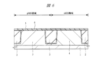
次に、本実施の形態における半導体装置を構成するnMISトランジスタQnおよびpMISトランジスタQpの製造方法について図面を参照して説明する。図6〜図18は本実施の形態における製造工程中の半導体装置の要部を模式的に示す断面図であり、図2のA−A’線におけるものである。 Next, a method for manufacturing the nMIS transistor Qn and the pMIS transistor Qp constituting the semiconductor device in the present embodiment will be described with reference to the drawings. 6 to 18 are cross-sectional views schematically showing the main part of the semiconductor device during the manufacturing process according to the present embodiment, and are taken along line A-A 'of FIG.
まず、例えばp型単結晶シリコンから構成される基板1を準備し、表面処理を施した後、図6および図2に示すように、基板1の主面(素子形成面)に活性領域を区画する素子分離領域2を形成する。本実施の形態では、素子分離領域2は、基板1に形成された例えば250nm〜400nm程度の深さの素子分離溝に、例えばCVD法を用いて埋め込まれた酸化シリコン膜から構成されるSTI(Shallow Trench Isolation)である。この素子分離領域2では、pMIS領域およびnMIS領域の境界が位置することとなる。このように、CMISの一方を構成するpMISトランジスタが形成されるpMIS領域と、CMISの他方を構成するnMISトランジスタが形成されるnMIS領域とを有する基板1を準備する。
First, a
続いて、図6および図2に示すように、基板1のpMIS領域にpMISトランジスタのpチャネルが生成されることとなるnウェル3を形成する。また、nMIS領域にnMISトランジスタのnチャネルが生成されることとなるpウェル4を形成する。nウェル3は、イオン注入法を用いて、リン(P)や砒素(As)などのn型不純物を基板1内に導入することにより形成される。また、pウェル4は、イオン注入法を用いて、ボロン(B)やフッ化ボロン(BF2)などのp型不純物を基板1内に導入することにより形成される。
Subsequently, as shown in FIGS. 6 and 2, an n-well 3 in which a p-channel of a pMIS transistor is to be generated is formed in the pMIS region of the
続いて、図6に示すように、基板1の主面上に、界面層として0.5nm程度の厚さで酸化シリコン膜(SiO2膜5)を形成する。基板1にシリコンを適用しているので、例えば、酸素雰囲気での熱処理を行うことによって、SiO2膜5が形成される。このSiO2膜5は、後の工程でSiO2膜5上に形成される高誘電率膜との界面にダイポール(電子双極子)を生成するため、MISトランジスタの実効仕事関数に影響を及ぼすものであると考えられる。
Subsequently, as shown in FIG. 6, a silicon oxide film (SiO 2 film 5) is formed on the main surface of the
続いて、図6に示すように、SiO2膜5上に、2〜3nm程度の厚さで酸化ハフニウム膜(HfO2膜6)を形成する。本実施の形態では、SiO2膜5より厚く、ハフニウム(Hf)および酸素(O)を含む膜状の基材(以下、ベース絶縁膜ともいう)としてHfO2膜6を形成している。HfO2膜6は、例えば、原子層制御成膜(ALD:Atomic Layer Deposition)法、CVD法あるいはスパッタ法を用いて形成される。このHfO2膜6は、酸化シリコンより誘電率が高いので、高誘電率膜である。後の工程で、基材であるこのHfO2膜6に金属元素が拡散(混合)されることとなる。必要に応じて製造途中、最後にHfO2膜6を窒化や熱処理しても良い。 Subsequently, as shown in FIG. 6, a hafnium oxide film (HfO 2 film 6) is formed on the SiO 2 film 5 with a thickness of about 2 to 3 nm. In the present embodiment, the HfO 2 film 6 is formed as a film-like base material (hereinafter also referred to as a base insulating film) that is thicker than the SiO 2 film 5 and contains hafnium (Hf) and oxygen (O). The HfO 2 film 6 is formed using, for example, an atomic layer control film formation (ALD: Atomic Layer Deposition) method, a CVD method, or a sputtering method. The HfO 2 film 6 is a high dielectric constant film because it has a dielectric constant higher than that of silicon oxide. In a later step, the metal element is diffused (mixed) into the HfO 2 film 6 which is a base material. If necessary, the HfO 2 film 6 may be nitrided or heat-treated at the end during the production.
続いて、図7に示すように、例えばスパッタ法を用いて、基板1上、すなわち基材であるHfO2膜6上に、0.5nm程度の厚さでアルミニウム膜(Al膜7)を形成する。本実施の形態では、基材であるHfO2膜6より薄く、かつ、金属元素のみからなる膜状の混合材(以下、金属薄膜ともいう)としてAl膜7を形成している。なお、後の工程で、混合材であるAl膜7の構成元素(金属元素)は、基材であるHfO2膜6に拡散されて、pMISトランジスタQpのゲート絶縁膜を構成することとなる。
Subsequently, as shown in FIG. 7, an aluminum film (Al film 7) is formed with a thickness of about 0.5 nm on the
本実施の形態では、pMISトランジスタQpのゲート絶縁膜を形成するために、絶縁性を示す金属酸化物や窒化物でははく、金属元素のみで構成される金属薄膜のAl膜7を用いている。金属薄膜に含まれる金属元素は、アルミニウム(Al)に限らず、チタン(Ti)、タンタル(Ta)であっても良い。これら金属元素は、図5の表に示したように、酸化ハフニウム(HfO2)より電気陰性度が大きい金属酸化物を構成するものである。このようなAl、Ti、Taのような金属元素を基材であるHfO2膜6に拡散(あるいは混合)することによって、pMISトランジスタQpのゲート絶縁膜を構成する高誘電率膜(混合膜)が形成される。
In this embodiment, in order to form the gate insulating film of the pMIS transistor Qp, a metal thin
続いて、図8に示すように、混合材であるAl膜7上に、10nm程度の窒化チタン膜(TiN膜)8を形成する。本実施の形態では、Al膜7を変質させない膜、すなわち、耐湿性および耐酸化性を有する保護膜として、また、後の工程で、混合材であるAl膜7の金属元素を、基材であるHfO2膜6に拡散させるためのアニール処理(熱処理)温度に耐える保護膜として、TiN膜8を適用している。
Subsequently, as shown in FIG. 8, a titanium nitride film (TiN film) 8 having a thickness of about 10 nm is formed on the
このように、金属薄膜(Al膜7)を変質させない膜であれば、窒化シリコン(SiN)膜も保護膜として適用することができる。しかしながら、本実施の形態では、以下の理由により、金属膜(金属保護膜)を用いている。 As described above, a silicon nitride (SiN) film can also be applied as a protective film as long as the metal thin film (Al film 7) is not altered. However, in the present embodiment, a metal film (metal protective film) is used for the following reason.
外気(O2やH2Oを含む)暴露に弱い混合材である金属薄膜を形成した同じ製造装置(例えば、スパッタ装置)において、真空度が保たれた状態で、連続成膜できることが望ましい。本実施の形態では、混合材である金属薄膜のAl膜7をスパッタ装置で形成しているので、スパッタ法を用いて連続成膜できる金属系のスパッタ膜としてAl膜7上に金属保護膜としてTiN膜8を形成している。これにより、金属薄膜のAl膜7により変質を与えることなく、安定した状態を保つことができる。
In the same manufacturing apparatus (for example, sputtering apparatus) in which a metal thin film that is a mixed material that is vulnerable to exposure to the outside air (including O 2 and H 2 O) is formed, it is desirable that continuous film formation can be performed while the degree of vacuum is maintained. In the present embodiment, the metal thin
また、金属保護膜としてTiN膜8を適用したのは、窒化チタンは、容易に除去できるウエット処理(薬液処理)材料が既知(例えばH2O2)であり、下地である金属薄膜のAl膜7にダメージを与えずに除去されるからである。なお、保護膜として、他の金属窒化物であってもウエット処理で除去することができ、下地の金属薄膜にダメージを与えないものであれば適用することができる。
The
続いて、図8に示すように、例えば450℃程度の温度でCVD法を用いて、TiN膜8上に、後のドライエッチング工程のハードマスクとして窒化シリコン膜(SiN膜)9を10nm程度形成する。次いで、フォトリソグラフィ技術を用いて、SiN膜9上にレジスト膜10を形成する(図9)。このレジスト膜10は、nMIS領域では除去されて、図9に示すように、pMIS領域のSiN膜9を覆うようなマスクとして用いられる。なお、図9で示す製造工程では、その断面状態ではSiN膜9上にレジスト膜10が設けられているように、その平面状態(図2参照)においてもpMIS領域にレジスト膜10が設けられている。
Subsequently, as shown in FIG. 8, a silicon nitride film (SiN film) 9 is formed on the
続いて、図9に示すように、レジスト膜10をマスクにしてnMIS領域のSiN膜9をドライエッチングによって除去し、ハードマスクとして機能を有するSiN膜9を形成する。その後、このレジスト膜10を例えばアッシングなどによって除去する。
Subsequently, as shown in FIG. 9, using the resist
続いて、図10に示すように、フォトリソグラフィ技術およびエッチング技術によって形成されたSiN膜9をハードマスクにしてnMIS領域のTiN膜8を、例えばH2O2および水洗によるウエットエッチングによって除去する。次いで、SiN膜9をハードマスクにしてnMIS領域のAl膜7を例えば希フッ酸(以下、dHFと記す)および水洗によるウエットエッチングによって除去する。これによって、nMIS領域のHfO2膜6が露出することとなる。このように、金属薄膜のAl膜7を保護膜のTiN膜8で覆い、そのTiN膜8と合わせてAl膜7を切り分けることによって、pMIS領域のみにpMISトランジスタのゲート電極材料を残すことができる。
Subsequently, as shown in FIG. 10, the
続いて、図11に示すように、例えばスパッタ法を用いて、基板1上、すなわち基材であるHfO2膜6上に、0.5nm程度の厚さでマグネシウム膜(Mg膜11)を形成する。本実施の形態では、基材であるHfO2膜6より薄く、かつ、金属元素のみからなる膜状の混合材(金属薄膜)としてMg膜11を形成している。これによりpMIS領域のHfO2膜6上にはAl膜7が設けられ、nMIS領域のHfO2膜6上にはpMIS領域の金属元素とは異なる金属元素のみからなるMg膜11が設けられている。なお、後の工程で、混合材であるMg膜11の構成元素(金属元素)は、基材であるHfO2膜6に拡散されて、nMISトランジスタQpのゲート絶縁膜を構成することとなる。
Subsequently, as shown in FIG. 11, a magnesium film (Mg film 11) is formed with a thickness of about 0.5 nm on the
本実施の形態では、nMISトランジスタQpのゲート絶縁膜を形成するために、絶縁性を示す金属酸化物や窒化物ではなく、金属元素のみで構成される金属薄膜のMg膜11を用いている。金属薄膜に含まれる単一の金属元素は、マグネシウム(Mg)に限らず、ランタン(La)、ガドリニウム(Gd)、イットリウム(Y)であっても良い。これら金属元素は、図5の表に示したように、酸化ハフニウム(HfO2)より電気陰性度が小さい金属酸化物を構成するものである。このようなMg、La、Gd、Yのような金属元素を基材であるHfO2膜6に拡散(あるいは混合)することによって、nMISトランジスタQpのゲート絶縁膜を構成する高誘電率膜(混合膜)が形成される。
In the present embodiment, in order to form the gate insulating film of the nMIS transistor Qp, the metal thin
続いて、図11に示すように、混合材であるMg膜11上に、10nm程度の窒化チタン膜(TiN膜)12を形成する。本実施の形態では、Mg膜11を変質させない膜、すなわち、耐湿性および耐酸化性を有する保護膜として、また、後の工程で、混合材であるMg膜11の金属元素を、基材であるHfO2膜6に拡散させるためのアニール処理(熱処理)温度に耐える保護膜として、TiN膜12を適用している。なお、本実施の形態において保護膜としてTiN膜12(金属保護膜)を用いている理由は前述したTiN膜8を用いる理由と同様である。
Subsequently, as shown in FIG. 11, a titanium nitride film (TiN film) 12 having a thickness of about 10 nm is formed on the
続いて、図11に示すように、例えば450℃程度の温度でCVD法を用いて、TiN膜12上に、後のドライエッチング工程のハードマスクとして窒化シリコン膜(SiN膜)13を10nm程度形成する。次いで、フォトリソグラフィ技術を用いて、SiN膜13上にレジスト膜14を形成する(図12参照)。このレジスト膜14は、pMIS領域では除去されて、図12に示すように、nMIS領域のSiN膜13を覆うようなマスクとして用いられる。なお、図12で示す製造工程では、その断面状態ではSiN膜13上にレジスト膜14が設けられているように、その平面状態(図2参照)においてもpMIS領域にレジスト膜14が設けられている。
Subsequently, as shown in FIG. 11, a silicon nitride film (SiN film) 13 is formed on the
続いて、図12に示すように、レジスト膜14をマスクにしてpMIS領域のSiN膜13をドライエッチングによって除去し、ハードマスクとして機能を有するSiN膜13を形成する。その後、このレジスト膜14を例えばアッシングなどによって除去する。
Subsequently, as shown in FIG. 12, the
続いて、図13に示すように、SiN膜13をハードマスクにしてpMIS領域のTiN膜12を、例えばH2O2および水洗によるウエットエッチングによって除去する。次いで、SiN膜13をハードマスクにしてpMIS領域のMg膜11を例えばdHFおよび水洗によるウエットエッチングによって除去する。これによって、pMIS領域のSiN膜9が露出することとなる。このように、金属薄膜のMg膜11を保護膜のTiN膜12で覆い、そのTiN膜12と合わせてMg膜12を切り分けることによって、nMIS領域のみにnMISトランジスタのゲート電極材料を残すことができる。
Subsequently, as shown in FIG. 13, using the
続いて、ハードマスクとして用いたSiN膜9およびSiN膜13をドライエッチングによって除去し、図14に示すように、pMIS領域ではTiN膜8を露出し、nMIS領域ではTiN膜12を露出する。なお、これらTiN膜8およびTiN膜12によって、pMIS領域ではAl膜7の表面が保護され、nMIS領域ではMg膜11の表面が保護されている。
Subsequently, the
続いて、pMIS領域では保護膜のTiN膜8を有し、nMIS領域では保護膜のTiN膜12を有する状態で、pMIS領域のHfO2膜6(ベース絶縁膜)に、Al膜7(金属薄膜)を構成する金属元素を拡散(あるいは混合)し、また、nMIS領域のHfO2膜6(ベース絶縁膜)に、Mg膜11(金属薄膜)を構成する金属元素を拡散(あるいは混合)する。
Subsequently, the pMIS region has a
これによって、図15に示すように、pMIS領域では、SiO2膜5上に、SiO2(酸化シリコン)よりも誘電率が高く、HfO2膜6(ベース絶縁膜)のハフニウム(Hf)および酸素(O)と、Al膜7(金属薄膜)の金属元素であるアルミニウム(Al)とを含む高誘電率膜(混合膜)のHfAlO膜6pを形成する。この高誘電率膜のHfAlO膜6pはpMISトランジスタQpのゲート絶縁膜を構成するものである(図3参照)。また、nMIS領域では、SiO2膜5上に、SiO2(酸化シリコン)よりも誘電率が高く、HfO2膜6(ベース絶縁膜)のハフニウム(Hf)および酸素(O)と、Mg膜11(金属薄膜)の金属元素であるマグネシウム(Mg)とを含む高誘電率膜(混合膜)のHfMgO膜6nを形成する。この高誘電率膜のHfMgO膜6nはnMISトランジスタQnのゲート絶縁膜を構成するものである(図3参照)。
Accordingly, as shown in FIG. 15, in the pMIS region, the dielectric constant is higher than that of SiO 2 (silicon oxide) on the SiO 2 film 5, and hafnium (Hf) and oxygen of the HfO 2 film 6 (base insulating film). A high dielectric constant film (mixed film)
本実施の形態では、ベース絶縁膜(HfO2膜6)に、金属元素のみからなる金属薄膜(Al膜7、Mg膜11)の金属元素を拡散させるために、ベース絶縁膜のHfO2膜6上に、金属元素のみからなる膜状の混合材、すなわち金属薄膜のAl膜7、Mg膜11を積層し、基板1に対して例えば600℃〜1000℃でアニール処理(熱処理)を行っている。これにより、高誘電率膜のHfAlO膜6p、HfMgO膜6nが形成される。
In this embodiment, the base insulating film (HfO 2 film 6), in order to diffuse the metal element of the metal thin film made of only a metal element (
図19は、本実施の形態における高誘電率膜の形成を説明するための図であり、nMISトランジスタの場合が示されている。なお、pMISトランジスタの場合も同様の工程で形成することができる。 FIG. 19 is a diagram for explaining the formation of a high dielectric constant film in the present embodiment, and shows the case of an nMIS transistor. Note that a pMIS transistor can be formed in the same process.
図19に示す構造は、前述したように、まず、シリコン(Si)からなる基板の主面上に、基板界面絶縁膜として酸化シリコン(SiO2)膜を形成し、その基板界面絶縁膜上に、ベース絶縁膜として酸化ハフニウム(HfO2)膜を形成する。次いで、スパッタ法によって、真空状態で金属薄膜としてマグネシウム(Mg)膜を形成し、同一装置内でその真空状態を保ったまま、すなわち大気開放しない状態で保護膜として窒化チタン(TiN)膜を積層形成する。その後、アニール処理をすることによって、ベース絶縁膜に金属薄膜の構成元素(金属元素)を拡散(あるいは混合)して、高誘電率膜(混合膜)としてHfMgO膜を形成する。なお、ベース絶縁膜は、ハフニウムおよび酸素を含む膜状の基材であり、金属薄膜は、ベース絶縁膜より薄く数nmあるいは1nm以下であり、かつ、金属元素のみからなる膜状の混合材である。 In the structure shown in FIG. 19, as described above, first, a silicon oxide (SiO 2 ) film is formed as a substrate interface insulating film on the main surface of a substrate made of silicon (Si), and the substrate interface insulating film is formed. Then, a hafnium oxide (HfO 2 ) film is formed as the base insulating film. Next, a magnesium (Mg) film is formed as a metal thin film in a vacuum state by sputtering, and a titanium nitride (TiN) film is laminated as a protective film while maintaining the vacuum state in the same apparatus, that is, without opening to the atmosphere. Form. Thereafter, by annealing, the constituent element (metal element) of the metal thin film is diffused (or mixed) into the base insulating film to form an HfMgO film as a high dielectric constant film (mixed film). Note that the base insulating film is a film-like base material containing hafnium and oxygen, and the metal thin film is a film-like mixed material that is thinner than the base insulating film and is several nm or 1 nm or less, and is made of only metal elements. is there.
ところで、MISトランジスを製造するにあたり、一般に、その製造工程中から、そのゲート絶縁膜には酸化膜を含む絶縁膜を適用し、そのゲート電極にはゲート絶縁膜に影響を及ぼさない金属膜を含む導電性膜が適用されている。これに対して、本実施の形態における金属元素のみからなる金属薄膜(Al膜7、Mg膜11)は、ゲート絶縁膜(高誘電率膜)の構成元素になるにも関わらず、製造工程中において、ベース絶縁膜(HfO2膜6)上に積層されている。また、金属薄膜すべてがゲート絶縁膜の構成元素になり残存しなくなる点で、金属薄膜は、ゲート電極を構成するものではない。
By the way, in manufacturing the MIS transistor, an insulating film including an oxide film is generally applied to the gate insulating film during the manufacturing process, and a metal film that does not affect the gate insulating film is included in the gate electrode. A conductive film is applied. On the other hand, the metal thin film (
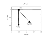
図30を参照して説明したように、基材となるベース絶縁膜102(例えば、HfO2膜)と、混合材となる別の薄い金属酸化膜103(例えば、MgO膜)とを積層した状態で、アニール処理することによって金属酸化膜103の構成元素をベース絶縁膜中に拡散させて、MISトランジスタの実効仕事関数、すなわち閾値を制御することができる。しかしながら、ベース絶縁膜102と金属酸化膜103の2つの絶縁膜を積層するため、EOTが厚くなり、絶縁容量がベース絶縁膜単独の容量値よりも小さくなってしまう。トランジスタの微細化において、これはゲート電界の制御特性を弱め、駆動能力などトランジスタ特性を劣化させてしまう。具体的に、図20を参照して説明する。
As described with reference to FIG. 30, the base insulating film 102 (for example, HfO 2 film) serving as a base material and another thin metal oxide film 103 (for example, MgO film) serving as a mixed material are stacked. Thus, by performing the annealing process, the constituent elements of the
図20は、HfO2のみのベース絶縁膜、Mg/HfO2をアニール処理してなる混合膜、およびMgO膜/HfO2をアニール処理してなる混合膜のEOTと、それらを用いたMISトランジスタの閾値(|ΔVth|)との関係を説明するための図である。なお、ベース絶縁膜のHfO2膜はEOTが1.0nmとなるものとし、金属酸化膜のMgO膜は物理膜厚が0.5nmとなるものとし、金属薄膜のMg膜は物理膜厚が0.5nmとしている。 Figure 20 is a base insulating film only HfO 2, Mg / a HfO 2 was annealed comprising mixed film, and the EOT of a mixed film of MgO film / HfO 2 formed by annealing of the MIS transistor using them It is a figure for demonstrating the relationship with a threshold value (| (DELTA) Vth |). Note that the base insulating film HfO 2 film has an EOT of 1.0 nm, the metal oxide film MgO film has a physical film thickness of 0.5 nm, and the metal thin film Mg film has a physical film thickness of 0 nm. .5 nm.
図20に示すように、基材となるベース絶縁膜のHfO2膜と、混合材となる別の薄い金属酸化膜のMgO膜とを積層した状態で、アニール処理することによって、金属酸化膜の構成元素をベース絶縁膜中に拡散させてなる混合膜(高誘電率膜)をゲート絶縁膜に用いることで、閾値を小さくすることができる。しかしながら、EOTが、HfO2膜と比較して増加してしまうため、トランジスタの微細化には好ましくない。 As shown in FIG. 20, by annealing the HfO 2 film of the base insulating film serving as the base material and the MgO film of another thin metal oxide film serving as the mixed material, the metal oxide film By using a mixed film (high dielectric constant film) formed by diffusing constituent elements in the base insulating film as the gate insulating film, the threshold value can be reduced. However, since EOT increases as compared with the HfO 2 film, it is not preferable for miniaturization of the transistor.
これに対して、本実施の形態に示すように、基材となるベース絶縁膜のHfO2膜と、混合材となる金属薄膜のMg膜とを積層した状態で、アニール処理することによって、金属薄膜の構成元素をベース絶縁膜中に拡散させてなる混合膜(高誘電率膜)をゲート絶縁膜に用いることで、閾値を小さくすることができ、またEOTもHfO2膜と比較して増加を抑制することができる。なお、図20ではベース絶縁膜のHfO2膜のEOTは1.0nmを用いたが、EOTが1.5nmのHfO2膜においても、若干傾きが変わるが、グラフの2本の直線は横軸のEOTが大きい方向に、ほぼ平行に移動し、同様の傾向を示す。 On the other hand, as shown in the present embodiment, by performing an annealing process in a state where the HfO 2 film of the base insulating film serving as the base material and the Mg film of the metal thin film serving as the mixed material are laminated, By using a mixed film (high dielectric constant film) formed by diffusing constituent elements of a thin film in the base insulating film as the gate insulating film, the threshold value can be reduced, and the EOT also increases compared to the HfO 2 film. Can be suppressed. In FIG. 20, although 1.0 nm is used for the EOT of the HfO 2 film of the base insulating film, the slope changes slightly even in the case of the HfO 2 film having an EOT of 1.5 nm. In the direction where the EOT is larger, the EOT moves almost in parallel and shows the same tendency.
従来においては、高誘電率膜を含んでゲート絶縁膜を構成する場合、EOTが増加しても、MISトランジスタの閾値を低減することは駆動させるためは重要と考えられていた。また、ゲート絶縁膜であるので、それを構成する材料も絶縁材料からなる膜でなければならないと考えられていた。これに対して、本実施の形態では、ゲート絶縁膜を構成する材料に、絶縁材料(金属酸化物)ではなく金属薄膜を用いることによって、EOTの増加を抑制しつつ、所望の閾値を制御している。 Conventionally, in the case of forming a gate insulating film including a high dielectric constant film, it has been considered to be important for driving to reduce the threshold value of the MIS transistor even if EOT increases. Moreover, since it is a gate insulating film, it was thought that the material which comprises it must also be a film | membrane which consists of insulating materials. On the other hand, in this embodiment, a desired threshold value is controlled while suppressing an increase in EOT by using a metal thin film instead of an insulating material (metal oxide) as a material constituting the gate insulating film. ing.
また、本実施の形態では、ベース絶縁膜上の金属薄膜は金属元素のみから構成されているので、酸素と結合し易い状態にある。このため、アニール処理によってベース絶縁膜を構成する酸化膜の酸素と結合するように、金属薄膜の金属元素がベース絶縁膜中に拡散しているものと考えられる。また、金属薄膜はベース絶縁膜より薄くすることによって、ゲート絶縁膜材料に金属元素のみからなる金属薄膜を用いても、その金属元素がすべてベース絶縁膜の酸素と結合する。このため、製造工程中に金属薄膜を用いたとしても、完成後にゲート絶縁膜として機能しないということはない。 In this embodiment mode, since the metal thin film over the base insulating film is composed of only the metal element, the metal thin film is likely to be bonded to oxygen. For this reason, it is considered that the metal element of the metal thin film is diffused in the base insulating film so as to be combined with oxygen of the oxide film constituting the base insulating film by the annealing treatment. Further, by making the metal thin film thinner than the base insulating film, even if a metal thin film made of only a metal element is used as the gate insulating film material, all the metal elements are bonded to oxygen of the base insulating film. For this reason, even if a metal thin film is used in the manufacturing process, it does not function as a gate insulating film after completion.
なお、ベース絶縁膜に金属元素を拡散させる方法として、ベース絶縁膜上に、その金属元素を含み、ベース絶縁膜に対して十分に厚いゲート電極材料を堆積させてアニール処理することも考えられる。このような方法ではアニール処理後であってもゲート電極材料は残存している。これに対して、本実施の形態では、ベース絶縁膜上に、それより薄い金属薄膜を堆積し、金属薄膜の金属元素をすべてベース絶縁膜中に拡散させるので、アニール処理後に金属薄膜は残存しないこととなる。また、金属薄膜の厚さを調整することでベース絶縁膜中に拡散させる金属元素の量を制御することができ、ゲート電極材料に含んだ金属元素をベース絶縁膜に拡散させる方法より制御性が優れている。 Note that as a method of diffusing a metal element into the base insulating film, it is also conceivable to deposit a gate electrode material that contains the metal element and is sufficiently thick on the base insulating film and then perform an annealing treatment. In such a method, the gate electrode material remains even after annealing. In contrast, in the present embodiment, a metal thin film thinner than that is deposited on the base insulating film, and all the metal elements of the metal thin film are diffused into the base insulating film, so that the metal thin film does not remain after annealing. It will be. In addition, the amount of metal element diffused into the base insulating film can be controlled by adjusting the thickness of the metal thin film, and the controllability is greater than the method of diffusing the metal element contained in the gate electrode material into the base insulating film. Are better.
このように、本実施の形態では、ゲート絶縁膜を構成する材料に、絶縁材料(金属酸化物)ではなく金属薄膜を用いることによって、EOTの増加を抑制しつつ、所望の閾値を制御している。したがって、金属薄膜を損傷、酸化などで変質させないことが重要となっている。そこで、本実施の形態では、金属薄膜上に保護膜を設けることによって、金属薄膜の酸化などの変質を防止している。具体的に、図21を参照して説明する。 As described above, in this embodiment, by using a metal thin film instead of an insulating material (metal oxide) as a material constituting the gate insulating film, a desired threshold value is controlled while suppressing an increase in EOT. Yes. Therefore, it is important not to alter the metal thin film due to damage, oxidation or the like. Therefore, in this embodiment, a protective film is provided on the metal thin film to prevent alteration such as oxidation of the metal thin film. Specifically, this will be described with reference to FIG.
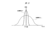
図21は、保護膜の有無によるMISトランジスタの閾値(Vth(V))のばらつきを説明するための図である。 FIG. 21 is a diagram for explaining variations in the threshold value (Vth (V)) of the MIS transistor depending on the presence or absence of the protective film.
例えばベース絶縁膜に、金属薄膜の構成元素を拡散させるために、ベース絶縁膜上に金属薄膜を積層した後、一旦、装置を換えるなどのために真空状態を脱した状態、すなわちウェハ(基板)が大気開放されることが考えられる。このため、数nmあるいは1nm以下の薄い金属薄膜は、大気暴露により酸化や膜の変質を受けやすく、トランジスタ特性のばらつきを引き起こしてしまう。 For example, in order to diffuse the constituent elements of the metal thin film into the base insulating film, the metal thin film is laminated on the base insulating film, and then the vacuum state is removed to change the device once, that is, the wafer (substrate). May be released to the atmosphere. For this reason, a thin metal thin film having a thickness of several nm or 1 nm or less is likely to be oxidized or deteriorated by exposure to the atmosphere, resulting in variations in transistor characteristics.
そこで本実施の形態では、ベース絶縁膜に金属薄膜の金属元素を拡散させるためにアニール処理を行うが、その際、それまで金属薄膜などを形成する製造装置から、アニール処理装置へ基板(ウェハ)を移動させることが考えられる。金属薄膜上に保護膜がない状態で基板を移動させた場合、O2やH2Oを含む外気暴露によって金属薄膜は酸化など変質してしまう。また、金属薄膜上に保護膜がない状態でレジスト膜を用いてパターニングした場合、そのレジスト膜を除去する際に金属薄膜の表面損傷などで変質してしまう。そこで、本実施の形態では、本実施の形態では、金属薄膜上に保護膜を設けることによって、金属薄膜の酸化などの変質を防止している。なお、図30を参照して説明したように、ベース絶縁膜に、金属酸化膜の構成元素を拡散させるなどのために、ベース絶縁膜上に金属酸化膜を積層した後、一旦、装置を換えるなどのために真空状態を脱する状態におく場合であっても、その金属酸化膜上に保護膜を設けることは、金属酸化膜の酸化などの変質を防止するために有効である。 Therefore, in this embodiment, annealing is performed to diffuse the metal element of the metal thin film into the base insulating film. At that time, from the manufacturing apparatus that forms the metal thin film or the like to the annealing processing apparatus up to that point, the substrate (wafer) Can be considered. When the substrate is moved in a state where there is no protective film on the metal thin film, the metal thin film is altered, such as oxidation, by exposure to the outside air containing O 2 and H 2 O. Further, when patterning is performed using a resist film without a protective film on the metal thin film, the resist film is altered due to surface damage of the metal thin film when the resist film is removed. Therefore, in this embodiment, in this embodiment, a protective film is provided on the metal thin film to prevent alteration such as oxidation of the metal thin film. As described with reference to FIG. 30, the metal oxide film is laminated on the base insulating film in order to diffuse the constituent elements of the metal oxide film into the base insulating film, and then the device is changed once. Even in the case of leaving the vacuum state for such reasons, it is effective to provide a protective film on the metal oxide film in order to prevent alteration such as oxidation of the metal oxide film.
また、本実施の形態では、例えば、スパッタ装置を用いて、真空状態において混合材となる金属薄膜を形成し、その真空状態を保ったままの状態(in-situ)で保護膜を形成している。このため、外気暴露によって金属薄膜の変質を抑制することができる。また、例えば、スパッタ装置を用いて、金属薄膜を形成し、その上に保護膜を形成した後、基板をアニール処理装置へ移した場合であっても、外気暴露によって金属薄膜の変質を抑制することができる。 In this embodiment, for example, a sputtering apparatus is used to form a metal thin film that becomes a mixed material in a vacuum state, and a protective film is formed in-situ while maintaining the vacuum state. Yes. For this reason, alteration of the metal thin film can be suppressed by exposure to the outside air. Further, for example, even when a metal thin film is formed using a sputtering apparatus, a protective film is formed thereon, and then the substrate is transferred to an annealing apparatus, the deterioration of the metal thin film is suppressed by exposure to the outside air. be able to.
また、例えば、スパッタ装置を用いて、真空状態において混合材となる金属薄膜を形成し、その真空状態を保ったままアニール処理を行うことによって、ベース絶縁膜に金属薄膜の金属元素を拡散し、混合膜(高誘電率膜)を形成することもできると考えられる。本実施の形態では、さらに、金属薄膜上に保護膜を設けることによって、アニール処理時に金属薄膜の金属元素が外方拡散するのを防止することができ、金属薄膜の構成元素すべてをベース絶縁膜に拡散することができるので、閾値の制御性を向上することができる。 In addition, for example, by using a sputtering apparatus, a metal thin film that is a mixed material in a vacuum state is formed, and annealing treatment is performed while maintaining the vacuum state, thereby diffusing the metal element of the metal thin film into the base insulating film, It is considered that a mixed film (high dielectric constant film) can also be formed. In the present embodiment, further, by providing a protective film on the metal thin film, it is possible to prevent the metal elements of the metal thin film from diffusing outwardly during the annealing process, and all the constituent elements of the metal thin film are made to be the base insulating film. Therefore, the controllability of the threshold can be improved.
また、本実施の形態では、金属薄膜上の保護膜として、窒化チタン(TiN)膜を適用している。TiN膜は容易に除去できる材料が既知(例えば、H2O2)であり、下地の金属薄膜にダメージを与えずに除去することができる。 In this embodiment, a titanium nitride (TiN) film is applied as a protective film on the metal thin film. A material that can be easily removed from the TiN film is known (for example, H 2 O 2 ), and can be removed without damaging the underlying metal thin film.
図21に示すように、金属薄膜上に保護膜を設けないで形成されたMISトランジスタでは閾値のばらつきに対し、金属薄膜上に保護膜を設けて形成したMISトランジスタでは閾値のばらつきを抑制することができる。 As shown in FIG. 21, the MIS transistor formed without the protective film on the metal thin film suppresses the threshold value variation, whereas the MIS transistor formed with the protective film provided on the metal thin film suppresses the threshold value variation. Can do.
本実施の形態では、ベース絶縁膜と金属薄膜を積層し、その金属薄膜上に保護膜を設けて、ベース絶縁膜に金属薄膜の構成元素を拡散させて、ゲート絶縁膜を構成する混合膜(高誘電率膜)を形成している。この保護膜を用いてMISトランジスタを形成することによって、混合膜の界面の損傷変質を抑制し、またアニール時の金属元素の外方拡散を抑制し、MISトランジスタの閾値のばらつきを抑制することができる。言い換えると、金属薄膜上に保護膜を設けることによって、金属薄膜の酸化などの変質を防止し、また、安定してベース絶縁膜に金属薄膜の金属元素を拡散することができる。 In this embodiment, a base insulating film and a metal thin film are stacked, a protective film is provided on the metal thin film, and a constituent element of the metal thin film is diffused in the base insulating film to form a mixed film that forms a gate insulating film ( High dielectric constant film). By forming a MIS transistor using this protective film, it is possible to suppress damage alteration at the interface of the mixed film, to suppress outward diffusion of metal elements during annealing, and to suppress variation in threshold values of the MIS transistor. it can. In other words, by providing a protective film on the metal thin film, alteration such as oxidation of the metal thin film can be prevented, and the metal element of the metal thin film can be stably diffused into the base insulating film.
このようなアニール処理をした後、図15に示す保護膜として用いたTiN膜8およびTiN膜12を、例えばH2O2および水洗によるウエットエッチングによって除去し、pMIS領域ではHfAlO膜6pを露出し、nMIS領域ではHfMgO膜6nを露出する。
After such annealing treatment, the
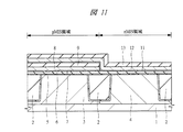
続いて、図16に示すように、ゲート電極材料を形成するにあたり、先の工程で形成されたAl膜7やMg膜11の金属膜と異なる導電性膜として、pMIS領域のHfAlO膜6p上に、およびnMIS領域のHfMgO膜6n上にTiN膜15およびポリシリコン膜16を形成する。本実施の形態では、ゲート電極材料として、まず、HfAlO膜6pおよびHfMgO膜6n上に、スパッタ法を用いて、5〜20nm程度のTiN膜15を形成し、その後、TiN膜15上に50〜100nm程度の導電性のポリシリコン膜16を形成する。なお、本実施の形態では、ゲート電極材料として窒化チタン(TiN)を適用しているが、窒化タンタル(TaN)であっても良い。
Subsequently, as shown in FIG. 16, when forming the gate electrode material, a conductive film different from the metal film of the
前述した保護膜として用いたTiN膜8、TiN膜12と、ゲート電極材料として用いたTiN膜15とは同じ窒化チタンであるため、TiN膜8、TiN膜12をアニール処理後、除去せずにゲート電極材料として用いることも考えられる。本実施の形態では、保護膜として用いたTiN膜8、TiN膜12の工程中のダメージを考慮して、ゲート電極材料として再度TiN膜15を形成している。
Since the
続いて、図17に示すように、導電性膜であるポリシリコン膜16、TiN膜15、混合膜であるHfAlO膜6p、HfMgO膜6n、基板界面絶縁膜であるSiO2膜5を、例えばフォトリソグラフィ技術およびエッチングによって所定の形状にパターニングする。これにより、pMIS領域では、ポリシリコン膜16およびTiN膜15から構成されるpMISトランジスタのゲート電極G、HfAlO膜6pおよびSiO2膜5から構成されるゲート絶縁膜を形成する。また、nMIS領域では、ポリシリコン膜16およびTiN膜15から構成されるnMISトランジスタのゲート電極G、HfMgO膜6nおよびSiO2膜5から構成されるゲート絶縁膜を形成する。なお、平面視したゲート電極Gが図2に示されている。
Subsequently, as shown in FIG. 17, a
続いて、図18に示すように、pMIS領域ではpMISトランジスタQpのp型半導体領域(ソース/ドレイン)17、nMIS領域ではnMISトランジスタQnのn型半導体領域(ソース/ドレイン)18を形成した後、ゲート電極の側面に沿ったサイドウォール19を形成し、ゲート電極G、p型半導体領域17、n型半導体領域18の表面にシリサイド膜20を形成する。
Subsequently, as shown in FIG. 18, after forming the p-type semiconductor region (source / drain) 17 of the pMIS transistor Qp in the pMIS region and the n-type semiconductor region (source / drain) 18 of the nMIS transistor Qn in the nMIS region, A
フォトリソグラフィ技術およびイオン注入技術を用いて、pMIS領域の基板1に例えばボロンなどのp型不純物を導入し、またnMIS領域の基板1に例えばリンや砒素などのn型不純物を導入した後、アニール処理を行うことによって、pMIS領域ではそのゲート電極に整合したp型半導体領域(ソース/ドレイン)17を形成し、またnMIS領域ではそのゲート電極に整合したn型半導体領域(ソース/ドレイン)18を形成する。これにより、pMIS領域ではpMISトランジスタQpが形成され、またnMIS領域ではnMISトランジスタQnが形成される。
Using a photolithography technique and an ion implantation technique, a p-type impurity such as boron is introduced into the
本実施の形態では、ベース絶縁膜に金属薄膜の構成元素を拡散させるためのアニール処理と、ソース/ドレインを形成するためのアニール処理とを別工程で行っている。なお、ベース絶縁膜に金属薄膜の構成元素を拡散させるためのアニール処理は、先の工程で行わず、このソース/ドレイン形成のためのアニール処理で兼用するができると考えられる。その場合、ゲート電極材料として適用するTiN膜が保護膜としての外方拡散防止などの機能を有する。 In the present embodiment, the annealing process for diffusing the constituent elements of the metal thin film in the base insulating film and the annealing process for forming the source / drain are performed in separate steps. Note that it is considered that the annealing process for diffusing the constituent elements of the metal thin film into the base insulating film is not performed in the previous step, but can be also used in the annealing process for forming the source / drain. In that case, a TiN film applied as a gate electrode material has a function of preventing outward diffusion as a protective film.
半導体装置の微細化によって、ソース/ドレインを構成する半導体領域の深さも、従来と比較して浅い位置で形成されるため、基板1に注入した不純物をその注入された位置で活性化する必要がある。そのため、本実施の形態では、ソース/ドレイン形成のためのアニール処理は、レーザーアニール、フラッシュアニールなどのRTA(RapidThermal Anneal)であり、1000℃程度、数ミリ秒間で行っている。これに対して、ベース絶縁膜に金属薄膜の構成元素を拡散させるためのアニール処理は、金属薄膜の構成元素すべてをベース絶縁膜に拡散させる必要があるため、RTAより時間は長いものとなる。したがって、本実施の形態では、ベース絶縁膜に金属薄膜の構成元素を拡散させるためのアニール処理と、ソース/ドレインを形成するためのアニール処理とを別工程で行っている。
Due to the miniaturization of the semiconductor device, the depth of the semiconductor region constituting the source / drain is also formed at a shallow position as compared with the conventional case. Therefore, it is necessary to activate the impurity implanted into the
サイドウォール19の形成は、nMIS領域およびpMIS領域を含む基板1上に、例えばCVD法によって窒化シリコン膜を形成し、その窒化シリコン膜を異方性エッチングすることにより、パターニングされたゲート電極Gの側壁に形成する。
The
シリサイド膜20の形成は、基板1の主面上に例えばニッケル膜を形成し、熱処理によって基板1およびゲート電極を構成するポリシリコン膜16のシリコンと反応(シリサイド化)させた後、未反応のニッケル膜を除去する。これによって、pMIS領域ではpMISトランジスタQpのゲート電極上およびp型半導体領域(ソース/ドレイン)17上にシリサイド膜20が形成され、nMIS領域ではnMISトランジスタQnのゲート電極上およびn型半導体領域(ソース/ドレイン)18上にシリサイド膜20が形成される。このシリサイド膜20により、後の工程で形成されるコンタクトとの接触抵抗を低減することができる。
The
続いて、図3に示すように、基板1の主面上に層間絶縁膜21を形成した後、所定の位置(図2参照)にコンタクトホール22を形成し、それに導電性材料を埋め込むことによってコンタクトCNTを形成する。その後、コンタクトCNTと電気的に接続した配線23を形成する。さらに、図示しないが、例えば、配線23の上層に多層配線を形成し、最表面にパッシベーション膜が形成されることによって、半導体装置が完成する。
Subsequently, as shown in FIG. 3, after an
層間絶縁膜21の形成は、例えば、CVD法を用いて酸化シリコン膜が堆積される。また、コンタクトホール22の形成は、フォトリソグラフィ技術およびエッチング技術を用いて、層間絶縁膜21を貫通し、ゲート電極G、p型半導体領域(ソース/ドレイン)17、およびn型半導体領域(ソース/ドレイン)18に達するように行われる。
The
また、コンタクトCNTの形成は、まず、コンタクトホール22の底面および内壁を含む層間絶縁膜21上に、例えばスパッタ法を用いてチタン/窒化チタン膜を形成した後、コンタクトホール22を埋め込むように基板1上に、例えばCVD法を用いてタングステン膜を形成する。次いで、層間絶縁膜21上に形成された不要なチタン/窒化チタン膜およびタングステン膜を例えばCMP法で除去することによって、コンタクトCNTが形成される。コンタクトCNTのチタン/窒化チタン膜は、タングステン膜中のタングステンがシリコン中へ拡散するのを防止する、いわゆるバリア性を有するものである。
The contact CNT is formed by first forming a titanium / titanium nitride film on the
また、配線23は、まず、層間絶縁膜21上およびコンタクトCNT上にチタン/窒化チタン膜、銅を含有するアルミニウム膜、チタン/窒化チタン膜を順次、形成する。これらの膜は、例えばスパッタ法を用いることにより形成することができる。次いで、フォトリソグラフィ技術およびエッチング技術を用いて、これらの膜のパターニングを行い、配線23を形成する。
For the
このようにして、基板1上にSRAMを含む集積回路を形成することができる。すなわち、本実施の形態では、SRAMを構成する駆動用MISトランジスタのnMISトランジスタQnと負荷用MISトランジスタのpMISトランジスタQpを図示して半導体装置の製造工程について説明したが、SRAMを構成するその他のMISトランジスタ(転送用MISトランジスタなどを含む)も基本的に同様な工程で形成される。以上のようにして、本実施の形態における半導体装置を製造することができる。
In this way, an integrated circuit including an SRAM can be formed on the
なお、pMISトランジスタQpおよびnMISトランジスタQnを製造していく工程の順番は逆になっても構わない。例えば、本実施の形態では、pMISトランジスタQpのゲート電極材料となるAl膜7を形成した後、nMISトランジスタQnのゲート電極材料となるMg膜11を形成しているが、その順番は逆であっても構わない。
Note that the order of the steps for manufacturing the pMIS transistor Qp and the nMIS transistor Qn may be reversed. For example, in this embodiment, after forming the
(実施の形態2)
前記実施の形態1では、pMISトランジスタQpのHfAlO膜6pと、nMISトランジスタQnのHfMgO膜6nの2種類の混合膜(高誘電率膜)を形成するために、それぞれに対応するAl膜7およびMg膜11の金属薄膜の切り分けに際し、レジスト膜10、14を用いたマスク合わせを2回行う場合について説明した。本実施の形態では、そのレジスト膜を用いたマスク合わせを1回省略する場合について説明する。それに伴う製造工程は前記実施の形態1と異なるが、最終構造は前記実施の形態1と同様となる。以下に、前記実施の形態1と相違する点を中心に説明する。図22〜図24は本実施の形態における製造工程中の半導体装置の要部を模式的に示す断面図である。
(Embodiment 2)
In the first embodiment, in order to form two types of mixed films (high dielectric constant films), that is, the
図10を参照して説明したように、フォトリソグラフィ技術およびエッチング技術によって形成されたSiN膜9をハードマスクにしてnMIS領域のTiN膜8、さらにはAl膜7を除去する。これによって、nMIS領域のHfO2膜6が露出することとなる。このように、金属薄膜のAl膜7を保護膜のTiN膜8で覆い、そのTiN膜8と合わせてAl膜7を切り分けることによって、pMIS領域のみにpMISトランジスタのゲート電極材料を残すことができる。その後、ハードマスクとして用いたSiN膜9をドライエッチングによって除去し、図22に示すように、pMIS領域ではTiN膜8を露出する。
As described with reference to FIG. 10, the
続いて、図23に示すように、例えばスパッタ法を用いて、基板1上、すなわち基材であるHfO2膜6上に、0.5nm程度の厚さでマグネシウム膜(Mg膜11)を形成する。本実施の形態では、基材であるHfO2膜6より薄く、かつ、金属元素のみからなる膜状の混合材(金属薄膜)としてMg膜11を形成している。これによりpMIS領域のHfO2膜6上にはAl膜7が設けられ、nMIS領域のHfO2膜6上にはpMIS領域の金属元素とは異なる金属元素のみからなるMg膜11が設けられている。
Subsequently, as shown in FIG. 23, a magnesium film (Mg film 11) is formed with a thickness of about 0.5 nm on the
続いて、図23に示すように、混合材であるMg膜11上に、10nm程度の窒化チタン膜(TiN膜)12を形成する。Mg膜11を変質させない膜、すなわち、耐湿性および耐酸化性を有する保護膜として、また、後の工程で、混合材であるMg膜11の金属元素を、基材であるHfO2膜6に拡散させるためのアニール処理(熱処理)温度に耐える保護膜として、TiN膜12を適用している。
Subsequently, as shown in FIG. 23, a titanium nitride film (TiN film) 12 of about 10 nm is formed on the
続いて、pMIS領域では保護膜のTiN膜8を有し、nMIS領域では保護膜のTiN膜12を有する状態で、pMIS領域のHfO2膜6(ベース絶縁膜)に、Al膜7(金属薄膜)を構成する金属元素を拡散(あるいは混合)し、また、nMIS領域のHfO2膜6(ベース絶縁膜)に、Mg膜11(金属薄膜)を構成する金属元素を拡散(あるいは混合)する。
Subsequently, the pMIS region has a
これによって、図24に示すように、pMIS領域では、SiO2膜5上に、SiO2(酸化シリコン)よりも誘電率が高く、HfO2膜6(ベース絶縁膜)のハフニウム(Hf)および酸素(O)と、Al膜7(金属薄膜)の金属元素であるアルミニウム(Al)とを含む高誘電率膜(混合膜)のHfAlO膜6pを形成する。この高誘電率膜のHfAlO膜6pはpMISトランジスタQpのゲート絶縁膜を構成するものである(図3参照)。また、nMIS領域では、SiO2膜5上に、SiO2(酸化シリコン)よりも誘電率が高く、HfO2膜6(ベース絶縁膜)のハフニウム(Hf)および酸素(O)と、Mg膜11(金属薄膜)の金属元素であるマグネシウム(Mg)とを含む高誘電率膜(混合膜)のHfMgO膜6nを形成する。この高誘電率膜のHfMgO膜6nはnMISトランジスタQnのゲート絶縁膜を構成するものである(図3参照)。
Accordingly, as shown in FIG. 24, in the pMIS region, the dielectric constant is higher than that of SiO 2 (silicon oxide) on the SiO 2 film 5, and hafnium (Hf) and oxygen of the HfO 2 film 6 (base insulating film). A high dielectric constant film (mixed film)
このようなアニール処理をした後、図24に示す保護膜として用いたTiN膜8およびTiN膜12を、例えばH2O2および水洗によるウエットエッチングによって除去し、pMIS領域ではHfAlO膜6pを露出し、nMIS領域ではHfMgO膜6nを露出する。その後、図16を参照して説明した工程へと続き、最終的に図3に示したような半導体装置が完成する。
After such annealing treatment, the
本実施の形態では、pMIS領域ではフォトリソグラフィ技術によるマスクを設けることによって、ベース絶縁膜(HfO2膜6)上に1つめの金属薄膜(Al膜7)を形成し、nMIS領域ではベース絶縁膜(例えばHfO2膜6)上に2つめの金属薄膜(Mg膜11)を形成した後、フォトリソグラフィ技術によるマスクを設けずにアニール処理を行い、ベース絶縁膜にそれぞれの金属薄膜の構成元素を拡散させている。 In this embodiment, a first metal thin film (Al film 7) is formed on the base insulating film (HfO 2 film 6) by providing a mask by a photolithography technique in the pMIS region, and the base insulating film in the nMIS region. After the second metal thin film (Mg film 11) is formed on (for example, the HfO 2 film 6), an annealing process is performed without providing a mask by photolithography, and the constituent elements of each metal thin film are applied to the base insulating film. It is spreading.
これにより、前記実施の形態1では、2種の高誘電率膜(HfAlO膜6p、HfMgO膜6n)を形成するために、金属薄膜の切り分けでマスク合わせが2回で形成していたものを1回にしてプロセスを簡略化し、かつ2枚マスクの境界部分が重ね合わせの程度(オーバーラップか離れれるか)によって、膜除去のしやすさが変わることにより除去条件を調整する手間が省かれ、製造コストを削減することができる。
As a result, in the first embodiment, in order to form two types of high dielectric constant films (
(実施の形態3)
前記実施の形態2では、ハードマスクとして用いたSiN膜9を除去し、pMIS領域で保護膜のTiN膜8を露出した後、nMIS領域に金属薄膜のMg膜11、保護膜のTiN膜12を形成する場合について説明した。本実施の形態では、ハードマスクとして用いたSiN膜9を除去せずに以降の工程を行う場合について説明する。それに伴う製造工程は前記実施の形態2と異なるが、最終構造は前記実施の形態2と同様となる。以下に、前記実施の形態2と相違する点を中心に説明する。図25〜図26は本実施の形態における製造工程中の半導体装置の要部を模式的に示す断面図である。
(Embodiment 3)
In the second embodiment, the
図10を参照して説明したように、フォトリソグラフィ技術およびエッチング技術によって形成されたSiN膜9をハードマスクにしてnMIS領域のTiN膜8、さらにはAl膜7を除去する。これによって、nMIS領域のHfO2膜6が露出することとなる。このように、金属薄膜のAl膜7を保護膜のTiN膜8で覆い、そのTiN膜8と合わせてAl膜7を切り分けることによって、pMIS領域のみにpMISトランジスタのゲート電極材料を残すことができる。
As described with reference to FIG. 10, the
続いて、図25に示すように、例えばスパッタ法を用いて、基板1上、すなわち基材であるHfO2膜6上に、0.5nm程度の厚さでマグネシウム膜(Mg膜11)を形成する。本実施の形態では、基材であるHfO2膜6より薄く、かつ、金属元素のみからなる膜状の混合材(金属薄膜)としてMg膜11を形成している。これによりpMIS領域のHfO2膜6上にはAl膜7が設けられ、nMIS領域のHfO2膜6上にはpMIS領域の金属元素とは異なる金属元素のみからなるMg膜11が設けられている。
Subsequently, as shown in FIG. 25, a magnesium film (Mg film 11) is formed with a thickness of about 0.5 nm on the
続いて、図25に示すように、混合材であるMg膜11上に、10nm程度の窒化チタン膜(TiN膜)12を形成する。Mg膜11を変質させない膜、すなわち、耐湿性および耐酸化性を有する保護膜として、また、後の工程で、混合材であるMg膜11の金属元素を、基材であるHfO2膜6に拡散させるためのアニール処理(熱処理)温度に耐える保護膜として、TiN膜12を適用している。
Subsequently, as shown in FIG. 25, a titanium nitride film (TiN film) 12 of about 10 nm is formed on the
続いて、pMIS領域では保護膜のTiN膜8を有し、nMIS領域では保護膜のTiN膜12を有する状態で、pMIS領域のHfO2膜6(ベース絶縁膜)に、Al膜7(金属薄膜)を構成する金属元素を拡散(あるいは混合)し、また、nMIS領域のHfO2膜6(ベース絶縁膜)に、Mg膜11(金属薄膜)を構成する金属元素を拡散(あるいは混合)する。
Subsequently, the pMIS region has a
これによって、図26に示すように、pMIS領域では、SiO2膜5上に、SiO2(酸化シリコン)よりも誘電率が高く、HfO2膜6(ベース絶縁膜)のハフニウム(Hf)および酸素(O)と、Al膜7(金属薄膜)の金属元素であるアルミニウム(Al)とを含む高誘電率膜(混合膜)のHfAlO膜6pを形成する。この高誘電率膜のHfAlO膜6pはpMISトランジスタQpのゲート絶縁膜を構成するものである(図3参照)。また、nMIS領域では、SiO2膜5上に、SiO2(酸化シリコン)よりも誘電率が高く、HfO2膜6(ベース絶縁膜)のハフニウム(Hf)および酸素(O)と、Mg膜11(金属薄膜)の金属元素であるマグネシウム(Mg)とを含む高誘電率膜(混合膜)のHfMgO膜6nを形成する。この高誘電率膜のHfMgO膜6nはnMISトランジスタQnのゲート絶縁膜を構成するものである(図3参照)。
Accordingly, as shown in FIG. 26, in the pMIS region, the dielectric constant is higher than that of SiO 2 (silicon oxide) on the SiO 2 film 5, and hafnium (Hf) and oxygen of the HfO 2 film 6 (base insulating film). A high dielectric constant film (mixed film)
このようなアニール処理をした後、図26に示す保護膜として用いたTiN膜8およびTiN膜12を、例えばH2O2および水洗によるウエットエッチングによって除去し、pMIS領域ではHfAlO膜6pを露出し、nMIS領域ではHfMgO膜6nを露出する。この際、pMIS領域では、TiN膜11/SiN膜9/TiN膜8をリフトオフで除去できる。前記実施の形態2では、図10を参照して説明したように、SiN膜9を除去する際に、nMIS領域のHfMgO膜6nの表面にダメージを与える場合があるが、本実施の形態のように、nMIS領域のTiN膜12を除去する際に、pMIS領域のTiN膜11/SiN膜9/TiN膜8を除去してしまうので、HfMgO膜6nの表面へのダメージを抑制することができる。
After such annealing treatment, the
ここで、金属保護膜としてTiN膜8、TiN膜12を適用したのは、窒化チタンは、容易に除去できるウエット処理(薬液処理)材料が既知(例えばH2O2)であり、下地であるHfAlO膜6pおよびHfMgO膜6nにダメージを与えずに除去されるからである。
Here, the
その後、図16を参照して説明した工程へと続き、最終的に図3に示したような半導体装置が完成する。 Thereafter, the process described with reference to FIG. 16 is continued, and finally the semiconductor device as shown in FIG. 3 is completed.
(実施の形態4)
前記実施の形態1では、例えば図19を参照して、大気暴露により金属薄膜の変質を抑制するために、金属薄膜(例えばMg膜)上に保護膜(例えばTiN膜)を設ける場合について、例えば図19を参照して説明した。本実施の形態では、この保護膜を設けずに、ベース絶縁膜に金属薄膜の金属元素を拡散させる場合について説明する。図27は、本実施の形態における高誘電率膜の形成を説明するための図であり、nMISトランジスタの場合が示されている。なお、前記実施の形態1とは相違する点を中心に説明し、pMISトランジスタの場合も同様の工程で形成することができるのでその説明は省略する。
(Embodiment 4)
In the first embodiment, referring to FIG. 19, for example, a case where a protective film (for example, a TiN film) is provided on a metal thin film (for example, Mg film) in order to suppress alteration of the metal thin film by exposure to the atmosphere, This has been described with reference to FIG. In this embodiment, a case where a metal element of a metal thin film is diffused into the base insulating film without providing this protective film will be described. FIG. 27 is a diagram for explaining the formation of the high dielectric constant film in the present embodiment, and shows the case of an nMIS transistor. The description will focus on differences from the first embodiment, and the description of the pMIS transistor is omitted because it can be formed in the same process.
図27に示す構造は、まず、シリコン(Si)からなる基板の主面上に、基板界面絶縁膜として酸化シリコン(SiO2)膜を形成し、その基板界面絶縁膜上に、ベース絶縁膜として酸化ハフニウム(HfO2)膜を形成する。次いで、スパッタ法によって、真空状態で金属薄膜としてマグネシウム(Mg)膜を形成する。次いで、金属薄膜の表面を窒化した後、窒素雰囲気(プラズマ状でも良い)でのアニール処理(熱処理)を行うことによって、ベース絶縁膜に金属薄膜の構成元素(金属元素)を拡散して、高誘電率膜(混合膜)としてHfMgO膜を形成する。なお、ベース絶縁膜は、ハフニウムおよび酸素を含む膜状の基材であり、金属薄膜は、ベース絶縁膜より薄く数nmあるいは1nm以下であり、かつ、金属元素のみからなる膜状の混合材である。 In the structure shown in FIG. 27, first, a silicon oxide (SiO 2 ) film is formed as a substrate interface insulating film on a main surface of a substrate made of silicon (Si), and a base insulating film is formed on the substrate interface insulating film. A hafnium oxide (HfO 2 ) film is formed. Next, a magnesium (Mg) film is formed as a metal thin film in a vacuum state by sputtering. Next, after nitriding the surface of the metal thin film, an annealing process (heat treatment) in a nitrogen atmosphere (which may be in a plasma state) is performed, so that the constituent elements (metal elements) of the metal thin film are diffused into the base insulating film. An HfMgO film is formed as a dielectric constant film (mixed film). Note that the base insulating film is a film-like base material containing hafnium and oxygen, and the metal thin film is a film-like mixed material that is thinner than the base insulating film and is several nm or 1 nm or less, and is made of only metal elements. is there.
このように金属薄膜の表面を窒化することによって、金属薄膜の変質を抑制することができる。なお、金属薄膜を形成した後、金属薄膜の表面を酸化し、さらに窒化した後、アニール処理によってベース絶縁膜に金属薄膜の構成元素(金属元素)を拡散して、高誘電率膜(混合膜)としてHfMgO膜を形成することも考えられる。金属薄膜の表面が酸化してしまうが、微量にベース絶縁膜に酸素を拡散させて、より金属薄膜の金属元素と反応させる場合に有効と考えられる。その場合であっても、酸化させた後に窒化を行うので金属薄膜の変質を抑制することができる。 By nitriding the surface of the metal thin film in this way, alteration of the metal thin film can be suppressed. After forming the metal thin film, the surface of the metal thin film is oxidized and further nitrided, and then the constituent element (metal element) of the metal thin film is diffused into the base insulating film by annealing treatment, so that the high dielectric constant film (mixed film) It is also conceivable to form an HfMgO film. Although the surface of the metal thin film is oxidized, it is considered effective when a small amount of oxygen is diffused into the base insulating film to be reacted with the metal element of the metal thin film. Even in that case, since the nitridation is performed after the oxidation, the deterioration of the metal thin film can be suppressed.
(実施の形態5)
前記実施の形態1では、例えば図19を参照して、大気暴露などにより金属薄膜の変質を抑制するために、金属薄膜(例えばMg膜)上のみに保護膜(例えばTiN膜)を設けた場合について説明した。本実施の形態では金属薄膜を保護膜で挟んで金属薄膜を保護する場合について説明する。図28は、本実施の形態における高誘電率膜の形成を説明するための図であり、nMISトランジスタの場合が示されている。なお、前記実施の形態1とは相違する点を中心に説明し、pMISトランジスタの場合も同様の工程で形成することができるのでその説明は省略する。
(Embodiment 5)
In the first embodiment, referring to FIG. 19, for example, a protective film (for example, a TiN film) is provided only on a metal thin film (for example, an Mg film) in order to suppress deterioration of the metal thin film due to atmospheric exposure or the like. Explained. In this embodiment, a case where a metal thin film is protected by sandwiching the metal thin film with a protective film will be described. FIG. 28 is a diagram for explaining the formation of a high dielectric constant film in the present embodiment, and shows the case of an nMIS transistor. The description will focus on differences from the first embodiment, and the description of the pMIS transistor is omitted because it can be formed in the same process.
図28に示す構造は、まず、シリコン(Si)からなる基板の主面上に基板界面絶縁膜として酸化シリコン(SiO2)膜を形成し、その基板界面絶縁膜上にベース絶縁膜(HfO2膜)を形成する。次いで、例えば、スパッタ法を用いて、ベース絶縁膜上に第1保護膜(TiN膜)を形成し、その真空状態を保ったまま、スパッタ法を用いて、金属薄膜としてマグネシウム(Mg)膜、さらに第2保護膜(TiN膜)を形成する。その後、アニール処理をすることによって、ベース絶縁膜に金属薄膜の構成元素(金属元素)を拡散(あるいは混合)して、混合膜(高誘電率膜)としてHfMgO膜を形成する。なお、ベース絶縁膜は、ハフニウムおよび酸素を含む膜状の基材であり、金属薄膜は、ベース絶縁膜より薄く数nmあるいは1nm以下であり、かつ、金属元素のみからなる膜状の混合材である。 In the structure shown in FIG. 28, first, a silicon oxide (SiO 2 ) film is formed as a substrate interface insulating film on the main surface of a substrate made of silicon (Si), and a base insulating film (HfO 2 ) is formed on the substrate interface insulating film. Film). Next, for example, a first protective film (TiN film) is formed on the base insulating film using a sputtering method, and a magnesium (Mg) film as a metal thin film is formed using the sputtering method while maintaining the vacuum state. Further, a second protective film (TiN film) is formed. Thereafter, annealing is performed to diffuse (or mix) the constituent elements (metal elements) of the metal thin film into the base insulating film to form an HfMgO film as a mixed film (high dielectric constant film). Note that the base insulating film is a film-like base material containing hafnium and oxygen, and the metal thin film is a film-like mixed material that is thinner than the base insulating film and is several nm or 1 nm or less, and is made of only metal elements. is there.
このように、金属薄膜を第1保護膜と第2保護膜で挟んでも良く、この積層膜をアニール処理することによって、ベース絶縁膜に金属薄膜の金属元素を容易に拡散することができる。 As described above, the metal thin film may be sandwiched between the first protective film and the second protective film, and by annealing the laminated film, the metal element of the metal thin film can be easily diffused into the base insulating film.
(実施の形態6)
前記実施の形態1では、例えば図19を参照して、大気暴露により金属薄膜の変質を抑制するために、金属薄膜(例えばMg膜)上に保護膜(例えばTiN膜)を設ける場合について、例えば図19を参照して説明した。本実施の形態では、ベース絶縁膜(例えばHfO2膜)上に保護膜(例えばTiN膜)を設け、基板界面絶縁膜(SiO2膜)とベース絶縁膜(HfO2膜)との間に金属薄膜(例えばMg膜)を設ける場合について説明する。図29は、本実施の形態における高誘電率膜の形成を説明するための図であり、nMISトランジスタの場合が示されている。なお、前記実施の形態1とは相違する点を中心に説明し、pMISトランジスタの場合も同様の工程で形成することができるのでその説明は省略する。
(Embodiment 6)
In the first embodiment, referring to FIG. 19, for example, a case where a protective film (for example, a TiN film) is provided on a metal thin film (for example, Mg film) in order to suppress alteration of the metal thin film by exposure to the atmosphere, This has been described with reference to FIG. In this embodiment, a protective film (for example, a TiN film) is provided on a base insulating film (for example, an HfO 2 film), and a metal is interposed between the substrate interface insulating film (SiO 2 film) and the base insulating film (HfO 2 film). A case where a thin film (for example, an Mg film) is provided will be described. FIG. 29 is a diagram for explaining the formation of the high dielectric constant film in the present embodiment, and shows the case of an nMIS transistor. The description will focus on differences from the first embodiment, and the description of the pMIS transistor is omitted because it can be formed in the same process.
図29に示す構造は、まず、シリコン(Si)からなる基板の主面上に基板界面絶縁膜として酸化シリコン(SiO2)膜を形成し、その基板界面絶縁膜上に、例えばスパッタ法を用いて、金属薄膜としてマグネシウム(Mg)膜を形成する。次いで、金属薄膜上にベース絶縁膜(HfO2膜)を形成し、そのベース絶縁膜上に例えばスパッタ法を用いて保護膜(TiN膜)を形成する。その後、アニール処理をすることによって、ベース絶縁膜に金属薄膜の構成元素(金属元素)を拡散(あるいは混合)して、混合膜(高誘電率膜)としてHfMgO膜を形成する。なお、ベース絶縁膜は、ハフニウムおよび酸素を含む膜状の基材であり、金属薄膜は、ベース絶縁膜より薄く数nmあるいは1nm以下であり、かつ、金属元素のみからなる膜状の混合材である。また、ベース絶縁膜のHfO2膜もスパッタ法を用いて形成する場合、真空状態を保ったまま連続して金属薄膜、ベース絶縁膜、保護膜を形成することができる。 In the structure shown in FIG. 29, first, a silicon oxide (SiO 2 ) film is formed as a substrate interface insulating film on the main surface of a substrate made of silicon (Si), and, for example, a sputtering method is used on the substrate interface insulating film. Then, a magnesium (Mg) film is formed as a metal thin film. Next, a base insulating film (HfO 2 film) is formed on the metal thin film, and a protective film (TiN film) is formed on the base insulating film by using, for example, a sputtering method. Thereafter, annealing is performed to diffuse (or mix) the constituent elements (metal elements) of the metal thin film into the base insulating film to form an HfMgO film as a mixed film (high dielectric constant film). Note that the base insulating film is a film-like base material containing hafnium and oxygen, and the metal thin film is a film-like mixed material that is thinner than the base insulating film and is several nm or 1 nm or less, and is made of only metal elements. is there. Further, when the HfO 2 film of the base insulating film is also formed by sputtering, a metal thin film, a base insulating film, and a protective film can be formed continuously while maintaining a vacuum state.
このように、基板界面絶縁膜上に金属薄膜を設けてアニール処理を行うことによって、基板界面絶縁膜付近の混合膜にダイポールを生成することができ、実効仕事関数の制御性を向上することができる。 Thus, by providing a metal thin film on the substrate interface insulating film and performing the annealing treatment, a dipole can be generated in the mixed film near the substrate interface insulating film, and the controllability of the effective work function can be improved. it can.
以上、本発明者によってなされた発明を実施の形態に基づき具体的に説明したが、本発明は前記実施の形態に限定されるものではなく、その要旨を逸脱しない範囲で種々変更可能であることはいうまでもない。 As mentioned above, the invention made by the present inventor has been specifically described based on the embodiment. However, the present invention is not limited to the embodiment, and various modifications can be made without departing from the scope of the invention. Needless to say.
例えば、前記実施の形態では、混合材として、マグネシウムやアルミニウムなどの金属単体材料を用いる場合について説明したが、nMISトランジスタのゲート絶縁膜を構成するために、マグネシウム/ランタン、マグネシウム/他の希土類金属などの酸化金属物の電気陰性度が酸化ハフニウムより小さい構成元素同士や、アルミニウム/タンタルなどの酸化金属物の電気陰性度が酸化ハフニウムより大きい構成元素同士の積層膜を用いることができる。さらに、マグネシウム/アルミニウムなどのように酸化金属物の電気陰性度が酸化ハフニウムより大きい構成元素と小さい構成元素との組合せた積層膜を用いることで、閾値の微調整をすることもできると考えられる。 For example, in the above embodiment, the case where a single metal material such as magnesium or aluminum is used as the mixture has been described. However, in order to form the gate insulating film of the nMIS transistor, magnesium / lanthanum, magnesium / other rare earth metals are used. It is possible to use a laminated film in which constituent elements such as metal oxides having an electronegativity lower than that of hafnium oxide or constituent elements in which an electronegativity of metal oxides such as aluminum / tantalum is higher than that of hafnium oxide are used. Further, it is considered that the threshold value can be finely adjusted by using a laminated film in which a component element having an electronegativity of a metal oxide such as magnesium / aluminum is larger than that of hafnium oxide and a component element having a smaller value. .
また、例えば、前記実施の形態では、CMISを構成するにあたり、単結晶Siからなる半導体基板に適用した場合について説明したが、単結晶Ge基板や、GaAs、SiCなどの化合物半導体基板やSOI(Silicon On Insulator)基板にも適用することができる。 Further, for example, in the above embodiment, the case where the CMIS is applied to a semiconductor substrate made of single crystal Si has been described. However, a single crystal Ge substrate, a compound semiconductor substrate such as GaAs or SiC, or SOI (Silicon) is described. On Insulator) substrate can also be applied.
また、例えば、前記実施の形態では、SRAMの製造技術を対象としているが、これに限定されるものではなく、例えば、ロジック回路を構成するCMISの製造技術にも適用することができる。 Further, for example, in the above-described embodiment, the SRAM manufacturing technique is targeted, but the present invention is not limited to this. For example, the present invention can also be applied to a CMIS manufacturing technique that constitutes a logic circuit.
本発明は、半導体装置、特に、CMISを備えた半導体装置の製造業に幅広く利用されるものである。 The present invention is widely used in the manufacturing industry of semiconductor devices, particularly semiconductor devices provided with CMIS.
1 基板
2 素子分離領域
3 nウェル
4 pウェル
5 SiO2膜
6 HfO2膜
6n HfMgO膜
6p HfAlO膜
7 Al膜
8 TiN膜
9 SiN膜
10 レジスト膜
11 Mg膜
12 TiN膜
13 SiN膜
14 レジスト膜
15 TiN膜
16 ポリシリコン膜
17 p型半導体領域(ソース/ドレイン)
18 n型半導体領域(ソース/ドレイン)
19 サイドウォール
20 シリサイド膜
21 層間絶縁膜
22 コンタクトホール
23 配線
101 基板
102 高誘電率膜
103 金属酸化膜
104 ゲート絶縁膜
105 ゲート電極
CNT コンタクト
G ゲート電極
Qn nMISトランジスタ
Qp pMISトランジスタ
1
18 n-type semiconductor region (source / drain)
19
Claims (13)
(a)半導体基板の主面上に、酸化シリコン膜を形成する工程;
(b)前記酸化シリコン膜上に、ハフニウムおよび酸素を含む膜状の基材を形成する工程;
(c)前記基材上に、前記基材より薄く、かつ、金属元素のみからなる膜状の混合材を形成する工程;
(d)前記混合材の表面を窒化した後にアニール処理を施し、前記基材に前記混合材を拡散することによって、前記酸化シリコン膜上に、酸化シリコンより誘電率が高く、前記基材のハフニウムおよび酸素と、前記混合材の金属元素とを含む混合膜を形成する工程;
(e)前記混合膜上に、導電性膜を形成する工程;
(f)前記導電性膜から構成されるゲート電極、前記混合膜および前記酸化シリコン膜から構成されるゲート絶縁膜を形成する工程。 A method of manufacturing a semiconductor device having a MIS transistor including the following steps:
(A) forming a silicon oxide film on the main surface of the semiconductor substrate;
(B) forming a film-like substrate containing hafnium and oxygen on the silicon oxide film;
(C) forming a film-like mixed material that is thinner than the substrate and made of only a metal element on the substrate;
(D) An annealing treatment is performed after nitriding the surface of the mixed material, and the mixed material is diffused into the base material, whereby a dielectric constant higher than that of silicon oxide is formed on the silicon oxide film, and hafnium of the base material And forming a mixed film containing oxygen and the metal element of the mixed material;
(E) forming a conductive film on the mixed film;
(F) forming a gate electrode composed of the conductive film, a gate insulating film composed of the mixed film and the silicon oxide film;
(a)半導体基板の主面上に、酸化シリコン膜を形成する工程;
(b)前記酸化シリコン膜上に、ハフニウムおよび酸素を含む膜状の基材を形成する工程;
(c)前記基材上に、前記基材より薄く、かつ、金属元素のみからなる膜状の混合材を形成する工程;
(d)前記混合材の表面を酸化した後にアニール処理を施し、前記基材に前記混合材を拡散することによって、前記酸化シリコン膜上に、酸化シリコンより誘電率が高く、前記基材のハフニウムおよび酸素と、前記混合材の金属元素とを含む混合膜を形成する工程;
(e)前記混合膜上に、導電性膜を形成する工程;
(f)前記導電性膜から構成されるゲート電極、前記混合膜および前記酸化シリコン膜から構成されるゲート絶縁膜を形成する工程。 A method of manufacturing a semiconductor device having a MIS transistor including the following steps:
(A) forming a silicon oxide film on the main surface of the semiconductor substrate;
(B) forming a film-like substrate containing hafnium and oxygen on the silicon oxide film;
(C) forming a film-like mixed material that is thinner than the substrate and made of only a metal element on the substrate;
(D) annealed after oxidizing the surface of the mixed material, by spreading the mixed material to the substrate, the silicon oxide film, a higher dielectric constant than silicon oxide, the substrate Forming a mixed film containing hafnium and oxygen and the metal element of the mixed material;
(E) forming a conductive film on the mixed film;
(F) forming a gate electrode composed of the conductive film, a gate insulating film composed of the mixed film and the silicon oxide film;
(a)半導体基板の主面上に、酸化シリコン膜を形成する工程;
(b)前記酸化シリコン膜上に、ハフニウムおよび酸素を含む膜状の基材を形成する工程;
(c)前記基材上に、前記基材より薄く、かつ、金属元素のみからなる膜状の混合材を形成する工程;
(d)前記混合材の表面を酸化し、さらに窒化した後にアニール処理を施し、前記基材に前記混合材を拡散することによって、前記酸化シリコン膜上に、酸化シリコンより誘電率が高く、前記基材のハフニウムおよび酸素と、前記混合材の金属元素とを含む混合膜を形成する工程;
(e)前記混合膜上に、導電性膜を形成する工程;
(f)前記導電性膜から構成されるゲート電極、前記混合膜および前記酸化シリコン膜から構成されるゲート絶縁膜を形成する工程。 A method of manufacturing a semiconductor device having a MIS transistor including the following steps:
(A) forming a silicon oxide film on the main surface of the semiconductor substrate;
(B) forming a film-like substrate containing hafnium and oxygen on the silicon oxide film;
(C) forming a film-like mixed material that is thinner than the substrate and made of only a metal element on the substrate;
(D) The surface of the mixed material is oxidized, further nitrided, and then subjected to an annealing treatment. By diffusing the mixed material into the base material, the dielectric constant is higher than that of silicon oxide on the silicon oxide film, Forming a mixed film containing hafnium and oxygen of the base material and a metal element of the mixed material;
(E) forming a conductive film on the mixed film;
(F) forming a gate electrode composed of the conductive film, a gate insulating film composed of the mixed film and the silicon oxide film;
(a)半導体基板の主面上に、酸化シリコン膜を形成する工程;
(b)前記酸化シリコン膜上に、ハフニウムおよび酸素を含む膜状の基材を形成する工程;
(c)前記基材上に、前記基材より薄く、かつ、金属元素のみからなる膜状の混合材を形成する工程;
(d)前記混合材上に、保護膜を形成する工程;
(e)前記保護膜を有する状態で、前記基材に前記混合材を拡散することによって、前記酸化シリコン膜上に、酸化シリコンより誘電率が高く、前記基材のハフニウムおよび酸素と、前記混合材の金属元素とを含む混合膜を形成する工程;
(f)前記工程(e)の後、前記保護膜を除去する工程;
(g)前記混合膜上に、導電性膜を形成する工程;
(h)前記導電性膜から構成されるゲート電極、前記混合膜および前記酸化シリコン膜から構成されるゲート絶縁膜を形成する工程。 A method of manufacturing a semiconductor device having a MIS transistor including the following steps:
(A) forming a silicon oxide film on the main surface of the semiconductor substrate;
(B) forming a film-like substrate containing hafnium and oxygen on the silicon oxide film;
(C) forming a film-like mixed material that is thinner than the substrate and made of only a metal element on the substrate;
(D) forming a protective film on the mixed material;
(E) By diffusing the mixed material into the base material in the state having the protective film, the dielectric constant is higher than that of silicon oxide on the silicon oxide film, and the mixed material contains hafnium and oxygen of the base material. Forming a mixed film containing a metal element of the material;
(F) a step of removing the protective film after the step (e);
(G) forming a conductive film on the mixed film;
(H) A step of forming a gate electrode composed of the conductive film, a gate insulating film composed of the mixed film and the silicon oxide film.
前記工程(c)において、酸化ハフニウムより電気陰性度が小さい酸化金属物を構成する金属元素からなる前記混合材を形成することを特徴とする請求項4記載の半導体装置の製造方法。 The MIS transistor is an n-channel type,
5. The method of manufacturing a semiconductor device according to claim 4, wherein, in the step (c), the mixed material made of a metal element constituting a metal oxide having an electronegativity smaller than that of hafnium oxide is formed.
前記工程(c)において、酸化ハフニウムより電気陰性度が大きい酸化金属物を構成する金属元素からなる前記混合材を形成することを特徴とする請求項4記載の半導体装置の製造方法。 The MIS transistor is a p-channel type,
5. The method of manufacturing a semiconductor device according to claim 4, wherein, in the step (c), the mixed material made of a metal element constituting a metal oxide having a higher electronegativity than hafnium oxide is formed.
(a)半導体基板の主面上に、酸化シリコン膜を形成する工程;
(b)前記酸化シリコン膜上に、ハフニウムおよび酸素を含む膜状の基材を形成する工程;
(c)前記基材上に、保護膜を形成する工程;
(d)前記保護膜上に、前記基材より薄く、かつ、金属元素のみからなる膜状の混合材を形成する工程;
(e)前記保護膜を有する状態で、前記基材に前記混合材を拡散することによって、前記酸化シリコン膜上に、酸化シリコンより誘電率が高く、前記基材のハフニウムおよび酸素と、前記混合材の金属元素とを含む混合膜を形成する工程;
(f)前記工程(e)の後、前記保護膜を除去する工程;
(g)前記混合膜上に、導電性膜を形成する工程;
(h)前記導電性膜から構成されるゲート電極、前記混合膜および前記酸化シリコン膜から構成されるゲート絶縁膜を形成する工程。 A method of manufacturing a semiconductor device having a MIS transistor including the following steps:
(A) forming a silicon oxide film on the main surface of the semiconductor substrate;
(B) forming a film-like substrate containing hafnium and oxygen on the silicon oxide film;
(C) forming a protective film on the substrate;
(D) forming a film-like mixed material made of only a metal element and thinner than the base material on the protective film;
(E) By diffusing the mixed material into the base material in the state having the protective film, the dielectric constant is higher than that of silicon oxide on the silicon oxide film, and the mixed material contains hafnium and oxygen of the base material. Forming a mixed film containing a metal element of the material;
(F) a step of removing the protective film after the step (e);
(G) forming a conductive film on the mixed film;
(H) A step of forming a gate electrode composed of the conductive film, a gate insulating film composed of the mixed film and the silicon oxide film.
(a)半導体基板の主面上に、酸化シリコン膜を形成する工程;
(b)前記酸化シリコン膜上に、ハフニウムおよび酸素を含む膜状の基材を形成する工程;
(c)前記基材上に、第1保護膜を形成する工程;
(d)前記第1保護膜上に、前記基材より薄く、かつ、金属元素のみからなる膜状の混合材を形成する工程;
(e)前記混合材上に、第2保護膜を形成する工程;
(f)前記第1保護膜および前記第2保護膜を有する状態で、前記基材に前記混合材を拡散することによって、前記酸化シリコン膜上に、酸化シリコンより誘電率が高く、前記基材のハフニウムおよび酸素と、前記混合材の金属元素とを含む混合膜を形成する工程;
(g)前記工程(f)の後、前記第2保護膜および前記第1保護膜を除去する工程;
(h)前記混合膜上に、導電性膜を形成する工程;
(i)前記導電性膜から構成されるゲート電極、前記混合膜および前記酸化シリコン膜から構成されるゲート絶縁膜を形成する工程。 A method of manufacturing a semiconductor device having a MIS transistor including the following steps:
(A) forming a silicon oxide film on the main surface of the semiconductor substrate;
(B) forming a film-like substrate containing hafnium and oxygen on the silicon oxide film;
(C) forming a first protective film on the substrate;
(D) forming a film-like mixed material made of only a metal element and thinner than the base material on the first protective film;
(E) forming a second protective film on the mixed material;
(F) In the state having the first protective film and the second protective film, by diffusing the mixed material into the base material, the dielectric constant is higher than that of silicon oxide on the silicon oxide film, and the base material Forming a mixed film containing hafnium and oxygen and a metal element of the mixed material;
(G) a step of removing the second protective film and the first protective film after the step (f);
(H) forming a conductive film on the mixed film;
(I) forming a gate electrode composed of the conductive film, a gate insulating film composed of the mixed film and the silicon oxide film;
(a)前記CMISの一方を構成する第1MISトランジスタが形成される第1領域と、前記CMISの他方を構成する第2MISトランジスタが形成される第2領域とを有する半導体基板を準備する工程;
(b)前記半導体基板の主面上に、酸化シリコン膜を形成する工程;
(c)前記酸化シリコン膜上に、ハフニウムおよび酸素を含む膜状の基材を形成する工程;
(d)前記基材上に、金属元素のみからなる膜状の第1混合材を形成する工程;
(e)前記第1混合材上に、第1保護膜を形成する工程;
(f)前記第2領域の前記第1保護膜および前記第1混合材を除去する工程;
(g)前記第2領域の前記基材上に、前記基材より薄く、かつ、前記第1混合材の金属元素とは異なる金属元素のみからなる膜状の第2混合材を形成する工程;
(h)前記第2混合材上に、第2保護膜を形成する工程;
(i)前記第1保護膜および前記第2保護膜を有する状態で、前記第1領域の前記基材に前記第1混合材を拡散すると共に、前記第2領域の前記基材に前記第2混合材を拡散することによって、
前記第1領域では、前記酸化シリコン膜上に、酸化シリコンより誘電率が高く、前記基材のハフニウムおよび酸素と、前記第1混合材の金属元素とを含む第1混合膜を形成し、
前記第2領域では、前記酸化シリコン膜上に、酸化シリコンより誘電率が高く、前記基材のハフニウムおよび酸素と、前記第2混合材の金属元素とを含む第2混合膜を形成する工程;
(j)前記工程(i)の後、前記第1保護膜および前記第2保護膜を除去する工程;
(k)前記第1混合膜および前記第2混合膜上に、導電性膜を形成する工程;
(l)前記導電性膜から構成される前記第1MISトランジスタのゲート電極、前記第1混合膜および前記酸化シリコン膜から構成される前記第1MISトランジスタのゲート絶縁膜を形成し、
前記導電性膜から構成される前記第2MISトランジスタのゲート電極、前記第2混合膜および前記酸化シリコン膜から構成される前記第2MISトランジスタのゲート絶縁膜を形成する工程。 Manufacturing method of semiconductor device provided with CMIS including the following steps:
(A) preparing a semiconductor substrate having a first region in which a first MIS transistor constituting one of the CMISs is formed and a second region in which a second MIS transistor constituting the other of the CMISs is formed;
(B) forming a silicon oxide film on the main surface of the semiconductor substrate;
(C) forming a film-like substrate containing hafnium and oxygen on the silicon oxide film;
(D) forming a film-like first mixed material made of only a metal element on the substrate;
(E) forming a first protective film on the first mixed material;
(F) removing the first protective film and the first mixed material in the second region;
(G) forming a film-like second mixed material on the base material in the second region, which is thinner than the base material and made of only a metal element different from the metal element of the first mixed material;
(H) forming a second protective film on the second mixed material;
(I) In the state having the first protective film and the second protective film, the first mixed material is diffused into the base material in the first region, and the second base material in the second region is By diffusing the mixed material,
In the first region, a first mixed film having a dielectric constant higher than that of silicon oxide and containing hafnium and oxygen of the base material and a metal element of the first mixed material is formed on the silicon oxide film,
Forming a second mixed film having a dielectric constant higher than that of silicon oxide and including hafnium and oxygen of the base material and a metal element of the second mixed material on the silicon oxide film in the second region;
(J) after the step (i), removing the first protective film and the second protective film;
(K) forming a conductive film on the first mixed film and the second mixed film;
(L) forming a gate electrode of the first MIS transistor composed of the conductive film, a gate insulating film of the first MIS transistor composed of the first mixed film and the silicon oxide film;
Forming a gate electrode of the second MIS transistor composed of the conductive film, a gate insulating film of the second MIS transistor composed of the second mixed film and the silicon oxide film;
前記工程(g)において、酸化ハフニウムより電気陰性度が小さい酸化金属物を構成する金属元素からなる前記第2混合材を形成することを特徴とする請求項12記載の半導体装置の製造方法。 In the step (d), the first mixed material composed of a metal element constituting a metal oxide having a greater electronegativity than hafnium oxide is formed,
13. The method of manufacturing a semiconductor device according to claim 12, wherein in the step (g), the second mixed material made of a metal element constituting a metal oxide having an electronegativity smaller than that of hafnium oxide is formed.
Priority Applications (4)
| Application Number | Priority Date | Filing Date | Title |
|---|---|---|---|
| JP2008208472A JP5314964B2 (en) | 2008-08-13 | 2008-08-13 | Manufacturing method of semiconductor device |
| TW098117118A TWI456697B (en) | 2008-08-13 | 2009-05-22 | Method of manufacturing semiconductor device and semiconductor device |
| CN2009101584767A CN101651120B (en) | 2008-08-13 | 2009-07-08 | Method of manufacturing semiconductor device and semiconductor device |
| US12/537,875 US8288221B2 (en) | 2008-08-13 | 2009-08-07 | Method of manufacturing semiconductor device and semiconductor device |
Applications Claiming Priority (1)
| Application Number | Priority Date | Filing Date | Title |
|---|---|---|---|
| JP2008208472A JP5314964B2 (en) | 2008-08-13 | 2008-08-13 | Manufacturing method of semiconductor device |
Publications (3)
| Publication Number | Publication Date |
|---|---|
| JP2010045210A JP2010045210A (en) | 2010-02-25 |
| JP2010045210A5 JP2010045210A5 (en) | 2011-09-15 |
| JP5314964B2 true JP5314964B2 (en) | 2013-10-16 |
Family
ID=41673309
Family Applications (1)
| Application Number | Title | Priority Date | Filing Date |
|---|---|---|---|
| JP2008208472A Expired - Fee Related JP5314964B2 (en) | 2008-08-13 | 2008-08-13 | Manufacturing method of semiconductor device |
Country Status (4)
| Country | Link |
|---|---|
| US (1) | US8288221B2 (en) |
| JP (1) | JP5314964B2 (en) |
| CN (1) | CN101651120B (en) |
| TW (1) | TWI456697B (en) |
Families Citing this family (17)
| Publication number | Priority date | Publication date | Assignee | Title |
|---|---|---|---|---|
| JP5329294B2 (en) * | 2009-04-30 | 2013-10-30 | ルネサスエレクトロニクス株式会社 | Manufacturing method of semiconductor device |
| US8399344B2 (en) * | 2009-10-07 | 2013-03-19 | Asm International N.V. | Method for adjusting the threshold voltage of a gate stack of a PMOS device |
| US8659155B2 (en) | 2009-11-05 | 2014-02-25 | Taiwan Semiconductor Manufacturing Company, Ltd. | Mechanisms for forming copper pillar bumps |
| US8343865B2 (en) * | 2010-01-21 | 2013-01-01 | Renesas Electronics Corporation | Semiconductor device having dual work function metal |
| JP2011176173A (en) * | 2010-02-25 | 2011-09-08 | Renesas Electronics Corp | Semiconductor device and method of manufacturing the same |
| JP5548550B2 (en) * | 2010-07-30 | 2014-07-16 | ルネサスエレクトロニクス株式会社 | Manufacturing method of semiconductor device |
| JP2012044013A (en) * | 2010-08-20 | 2012-03-01 | Renesas Electronics Corp | Manufacturing method of semiconductor device |
| JP2013098214A (en) * | 2011-10-28 | 2013-05-20 | Elpida Memory Inc | Semiconductor device and manufacturing method of the same |
| JP5638559B2 (en) | 2012-03-26 | 2014-12-10 | 株式会社東芝 | Semiconductor device |
| JP5823353B2 (en) * | 2012-06-20 | 2015-11-25 | 株式会社東芝 | Method for manufacturing nonvolatile semiconductor memory device |
| EP2717308A1 (en) * | 2012-10-08 | 2014-04-09 | Imec | A method for manufacturing a dual work function semiconductor device |
| KR20140122585A (en) * | 2013-04-10 | 2014-10-20 | 삼성전자주식회사 | Semiconductor device and method for fabricating the same |
| US9263270B2 (en) * | 2013-06-06 | 2016-02-16 | Globalfoundries Inc. | Method of forming a semiconductor device structure employing fluorine doping and according semiconductor device structure |
| JP6581446B2 (en) * | 2015-09-09 | 2019-09-25 | 東芝メモリ株式会社 | Insulating film and memory device |
| JP2017092191A (en) * | 2015-11-06 | 2017-05-25 | 株式会社デンソー | Silicon carbide semiconductor device |
| CN106952917A (en) * | 2016-01-07 | 2017-07-14 | 中国科学院上海微系统与信息技术研究所 | A kind of layer transistor SRAM units of SOI six and preparation method thereof |
| CN113809012B (en) * | 2020-06-12 | 2024-02-09 | 长鑫存储技术有限公司 | Semiconductor device and method for manufacturing the same |
Family Cites Families (21)
| Publication number | Priority date | Publication date | Assignee | Title |
|---|---|---|---|---|
| JPH11135774A (en) * | 1997-07-24 | 1999-05-21 | Texas Instr Inc <Ti> | High-dielectric constant silicate gate dielectric |
| JP3944367B2 (en) * | 2001-02-06 | 2007-07-11 | 松下電器産業株式会社 | Method for forming insulating film and method for manufacturing semiconductor device |
| JP4895430B2 (en) * | 2001-03-22 | 2012-03-14 | ルネサスエレクトロニクス株式会社 | Semiconductor device and manufacturing method of semiconductor device |
| US7326988B2 (en) * | 2002-07-02 | 2008-02-05 | Matsushita Electric Industrial Co., Ltd. | Semiconductor device and method for fabricating the same |
| AU2003281112A1 (en) * | 2002-07-16 | 2004-02-02 | Nec Corporation | Semiconductor device, production method and production device thereof |
| WO2005038929A1 (en) * | 2003-10-15 | 2005-04-28 | Nec Corporation | Method for manufacturing semiconductor device |
| US6897095B1 (en) * | 2004-05-12 | 2005-05-24 | Freescale Semiconductor, Inc. | Semiconductor process and integrated circuit having dual metal oxide gate dielectric with single metal gate electrode |
| JP4005055B2 (en) * | 2004-05-25 | 2007-11-07 | Necエレクトロニクス株式会社 | Semiconductor device and manufacturing method thereof |
| US7060568B2 (en) * | 2004-06-30 | 2006-06-13 | Intel Corporation | Using different gate dielectrics with NMOS and PMOS transistors of a complementary metal oxide semiconductor integrated circuit |
| JP4792716B2 (en) | 2004-07-06 | 2011-10-12 | 日本電気株式会社 | Semiconductor device and manufacturing method thereof |
| US7087476B2 (en) * | 2004-07-28 | 2006-08-08 | Intel Corporation | Using different gate dielectrics with NMOS and PMOS transistors of a complementary metal oxide semiconductor integrated circuit |
| JP4372024B2 (en) * | 2005-02-14 | 2009-11-25 | 株式会社東芝 | CMOS semiconductor device |
| JP2006295131A (en) * | 2005-03-17 | 2006-10-26 | Renesas Technology Corp | Semiconductor apparatus and method for manufacturing same |
| JP4850458B2 (en) | 2005-09-12 | 2012-01-11 | 富士通セミコンダクター株式会社 | Semiconductor device and manufacturing method thereof |
| JP2007080995A (en) * | 2005-09-13 | 2007-03-29 | Toshiba Corp | Semiconductor device |
| JP2007243009A (en) * | 2006-03-10 | 2007-09-20 | Renesas Technology Corp | Semiconductor device and its manufacturing method |
| WO2007116470A1 (en) * | 2006-03-31 | 2007-10-18 | Fujitsu Limited | Semiconductor device and process for producing the same |
| WO2007138693A1 (en) * | 2006-05-31 | 2007-12-06 | Fujitsu Limited | Semiconductor device and method for manufacturing same |
| JP4282691B2 (en) * | 2006-06-07 | 2009-06-24 | 株式会社東芝 | Semiconductor device |
| JP2008311464A (en) * | 2007-06-15 | 2008-12-25 | National Institute Of Advanced Industrial & Technology | Semiconductor device and its manufacturing method |
| TWI492367B (en) * | 2007-12-03 | 2015-07-11 | Renesas Electronics Corp | Method of manufacturing cmos semiconductor device |
-
2008
- 2008-08-13 JP JP2008208472A patent/JP5314964B2/en not_active Expired - Fee Related
-
2009
- 2009-05-22 TW TW098117118A patent/TWI456697B/en not_active IP Right Cessation
- 2009-07-08 CN CN2009101584767A patent/CN101651120B/en active Active
- 2009-08-07 US US12/537,875 patent/US8288221B2/en not_active Expired - Fee Related
Also Published As
| Publication number | Publication date |
|---|---|
| CN101651120B (en) | 2013-10-02 |
| US20100038729A1 (en) | 2010-02-18 |
| JP2010045210A (en) | 2010-02-25 |
| US8288221B2 (en) | 2012-10-16 |
| TWI456697B (en) | 2014-10-11 |
| CN101651120A (en) | 2010-02-17 |
| TW201013847A (en) | 2010-04-01 |
Similar Documents
| Publication | Publication Date | Title |
|---|---|---|
| JP5314964B2 (en) | Manufacturing method of semiconductor device | |
| JP5128121B2 (en) | High performance CMOS circuit and manufacturing method thereof | |
| US7732872B2 (en) | Integration scheme for multiple metal gate work function structures | |
| JP5550286B2 (en) | Manufacturing method of semiconductor device | |
| US7863127B2 (en) | Manufacturing method of semiconductor device | |
| US20150102418A1 (en) | Semiconductor device and method for manufacturing the device | |
| CN101123252B (en) | Semiconductor device and manufacturing method thereof | |
| US9431498B2 (en) | Semiconductor device including first and second MISFETs | |
| TWI469262B (en) | Manufacturing method of semiconductor device and semiconductor device | |
| JP2007005721A (en) | Semiconductor device and manufacturing method thereof | |
| JP2008124393A (en) | Method of manufacturing semiconductor device | |
| US20080283928A1 (en) | Semiconductor device and manufacturing method thereof | |
| WO2011057492A1 (en) | Semiconductor device and manufacturing method thereof | |
| KR102434987B1 (en) | Method of forming a film and fabrication method of a semiconductor device | |
| US20110284971A1 (en) | Semiconductor device and manufacturing method thereof | |
| US20100252888A1 (en) | Semiconductor device | |
| TW202234595A (en) | Semiconductor structure | |
| JP2009267180A (en) | Semiconductor device | |
| JP2011003717A (en) | Semiconductor apparatus and method of manufacturing the same | |
| JP5291992B2 (en) | Manufacturing method of semiconductor device | |
| JP4163164B2 (en) | Semiconductor device and manufacturing method thereof | |
| JP2010062499A (en) | Semiconductor device and method of manufacturing semiconductor device | |
| JP2008066715A (en) | Semiconductor device and manufacturing method therefor | |
| JP2013118311A (en) | Semiconductor device manufacturing method | |
| US20120068275A1 (en) | Semiconductor device and method for fabricating the same |
Legal Events
| Date | Code | Title | Description |
|---|---|---|---|
| A711 | Notification of change in applicant |
Free format text: JAPANESE INTERMEDIATE CODE: A712 Effective date: 20100528 |
|
| A521 | Request for written amendment filed |
Free format text: JAPANESE INTERMEDIATE CODE: A523 Effective date: 20110801 |
|
| A621 | Written request for application examination |
Free format text: JAPANESE INTERMEDIATE CODE: A621 Effective date: 20110801 |
|
| A977 | Report on retrieval |
Free format text: JAPANESE INTERMEDIATE CODE: A971007 Effective date: 20130222 |
|
| A131 | Notification of reasons for refusal |
Free format text: JAPANESE INTERMEDIATE CODE: A131 Effective date: 20130305 |
|
| A521 | Request for written amendment filed |
Free format text: JAPANESE INTERMEDIATE CODE: A523 Effective date: 20130422 |
|
| TRDD | Decision of grant or rejection written | ||
| A01 | Written decision to grant a patent or to grant a registration (utility model) |
Free format text: JAPANESE INTERMEDIATE CODE: A01 Effective date: 20130611 |
|
| A61 | First payment of annual fees (during grant procedure) |
Free format text: JAPANESE INTERMEDIATE CODE: A61 Effective date: 20130708 |
|
| R150 | Certificate of patent or registration of utility model |
Free format text: JAPANESE INTERMEDIATE CODE: R150 Ref document number: 5314964 Country of ref document: JP Free format text: JAPANESE INTERMEDIATE CODE: R150 |
|
| S531 | Written request for registration of change of domicile |
Free format text: JAPANESE INTERMEDIATE CODE: R313531 |
|
| R350 | Written notification of registration of transfer |
Free format text: JAPANESE INTERMEDIATE CODE: R350 |
|
| LAPS | Cancellation because of no payment of annual fees |