EP2717308A1 - A method for manufacturing a dual work function semiconductor device - Google Patents
A method for manufacturing a dual work function semiconductor device Download PDFInfo
- Publication number
- EP2717308A1 EP2717308A1 EP12187571.0A EP12187571A EP2717308A1 EP 2717308 A1 EP2717308 A1 EP 2717308A1 EP 12187571 A EP12187571 A EP 12187571A EP 2717308 A1 EP2717308 A1 EP 2717308A1
- Authority
- EP
- European Patent Office
- Prior art keywords
- metal layer
- layer
- work function
- stack
- metal
- Prior art date
- Legal status (The legal status is an assumption and is not a legal conclusion. Google has not performed a legal analysis and makes no representation as to the accuracy of the status listed.)
- Withdrawn
Links
- 238000000034 method Methods 0.000 title claims abstract description 42
- 239000004065 semiconductor Substances 0.000 title claims abstract description 12
- 238000004519 manufacturing process Methods 0.000 title claims abstract description 8
- 230000009977 dual effect Effects 0.000 title claims abstract description 6
- 229910052751 metal Inorganic materials 0.000 claims abstract description 142
- 239000002184 metal Substances 0.000 claims abstract description 142
- 239000000758 substrate Substances 0.000 claims abstract description 35
- 238000009792 diffusion process Methods 0.000 claims abstract description 19
- ATJFFYVFTNAWJD-UHFFFAOYSA-N Tin Chemical compound [Sn] ATJFFYVFTNAWJD-UHFFFAOYSA-N 0.000 claims description 29
- 229910004481 Ta2O3 Inorganic materials 0.000 claims description 8
- 238000002955 isolation Methods 0.000 claims description 8
- 229910044991 metal oxide Inorganic materials 0.000 claims description 8
- 150000004706 metal oxides Chemical class 0.000 claims description 8
- 229910052782 aluminium Inorganic materials 0.000 claims description 6
- 238000000151 deposition Methods 0.000 claims description 5
- MRELNEQAGSRDBK-UHFFFAOYSA-N lanthanum oxide Inorganic materials [O-2].[O-2].[O-2].[La+3].[La+3] MRELNEQAGSRDBK-UHFFFAOYSA-N 0.000 claims description 5
- KTUFCUMIWABKDW-UHFFFAOYSA-N oxo(oxolanthaniooxy)lanthanum Chemical compound O=[La]O[La]=O KTUFCUMIWABKDW-UHFFFAOYSA-N 0.000 claims description 5
- MCMNRKCIXSYSNV-UHFFFAOYSA-N Zirconium dioxide Chemical compound O=[Zr]=O MCMNRKCIXSYSNV-UHFFFAOYSA-N 0.000 claims description 4
- XAGFODPZIPBFFR-UHFFFAOYSA-N aluminium Chemical compound [Al] XAGFODPZIPBFFR-UHFFFAOYSA-N 0.000 claims description 3
- 238000005530 etching Methods 0.000 claims description 2
- CJNBYAVZURUTKZ-UHFFFAOYSA-N hafnium(IV) oxide Inorganic materials O=[Hf]=O CJNBYAVZURUTKZ-UHFFFAOYSA-N 0.000 claims description 2
- TWNQGVIAIRXVLR-UHFFFAOYSA-N oxo(oxoalumanyloxy)alumane Chemical compound O=[Al]O[Al]=O TWNQGVIAIRXVLR-UHFFFAOYSA-N 0.000 claims description 2
- 239000000463 material Substances 0.000 description 17
- VYPSYNLAJGMNEJ-UHFFFAOYSA-N Silicium dioxide Chemical compound O=[Si]=O VYPSYNLAJGMNEJ-UHFFFAOYSA-N 0.000 description 13
- XUIMIQQOPSSXEZ-UHFFFAOYSA-N Silicon Chemical compound [Si] XUIMIQQOPSSXEZ-UHFFFAOYSA-N 0.000 description 11
- 229910052710 silicon Inorganic materials 0.000 description 11
- 239000010703 silicon Substances 0.000 description 11
- 150000004767 nitrides Chemical class 0.000 description 7
- -1 TaSix Inorganic materials 0.000 description 5
- 239000000654 additive Substances 0.000 description 5
- 230000000996 additive effect Effects 0.000 description 5
- PNEYBMLMFCGWSK-UHFFFAOYSA-N aluminium oxide Inorganic materials [O-2].[O-2].[O-2].[Al+3].[Al+3] PNEYBMLMFCGWSK-UHFFFAOYSA-N 0.000 description 5
- 229910052681 coesite Inorganic materials 0.000 description 5
- 229910052593 corundum Inorganic materials 0.000 description 5
- 229910052906 cristobalite Inorganic materials 0.000 description 5
- 229910052682 stishovite Inorganic materials 0.000 description 5
- 229910052905 tridymite Inorganic materials 0.000 description 5
- 238000007704 wet chemistry method Methods 0.000 description 5
- 229910001845 yogo sapphire Inorganic materials 0.000 description 5
- 230000015572 biosynthetic process Effects 0.000 description 4
- 238000001020 plasma etching Methods 0.000 description 4
- 239000000377 silicon dioxide Substances 0.000 description 4
- 229910052814 silicon oxide Inorganic materials 0.000 description 4
- 229910019044 CoSix Inorganic materials 0.000 description 3
- 229910015711 MoOx Inorganic materials 0.000 description 3
- 229910005889 NiSix Inorganic materials 0.000 description 3
- 229910019897 RuOx Inorganic materials 0.000 description 3
- 229910000577 Silicon-germanium Inorganic materials 0.000 description 3
- 229910008486 TiSix Inorganic materials 0.000 description 3
- 239000002019 doping agent Substances 0.000 description 3
- 230000010354 integration Effects 0.000 description 3
- 229910052761 rare earth metal Inorganic materials 0.000 description 3
- 229910021332 silicide Inorganic materials 0.000 description 3
- FVBUAEGBCNSCDD-UHFFFAOYSA-N silicide(4-) Chemical compound [Si-4] FVBUAEGBCNSCDD-UHFFFAOYSA-N 0.000 description 3
- JBRZTFJDHDCESZ-UHFFFAOYSA-N AsGa Chemical compound [As]#[Ga] JBRZTFJDHDCESZ-UHFFFAOYSA-N 0.000 description 2
- 229910052769 Ytterbium Inorganic materials 0.000 description 2
- 229910052784 alkaline earth metal Inorganic materials 0.000 description 2
- 150000001342 alkaline earth metals Chemical class 0.000 description 2
- 239000003990 capacitor Substances 0.000 description 2
- 238000012512 characterization method Methods 0.000 description 2
- 238000005516 engineering process Methods 0.000 description 2
- 239000011521 glass Substances 0.000 description 2
- 239000007943 implant Substances 0.000 description 2
- 239000012212 insulator Substances 0.000 description 2
- 239000011159 matrix material Substances 0.000 description 2
- 238000005259 measurement Methods 0.000 description 2
- 150000002736 metal compounds Chemical class 0.000 description 2
- 150000002739 metals Chemical class 0.000 description 2
- 238000004377 microelectronic Methods 0.000 description 2
- 239000000203 mixture Substances 0.000 description 2
- ZKATWMILCYLAPD-UHFFFAOYSA-N niobium pentoxide Chemical compound O=[Nb](=O)O[Nb](=O)=O ZKATWMILCYLAPD-UHFFFAOYSA-N 0.000 description 2
- 230000003647 oxidation Effects 0.000 description 2
- 238000007254 oxidation reaction Methods 0.000 description 2
- 238000000059 patterning Methods 0.000 description 2
- 229910052697 platinum Inorganic materials 0.000 description 2
- 150000002910 rare earth metals Chemical class 0.000 description 2
- 229910052707 ruthenium Inorganic materials 0.000 description 2
- 230000005641 tunneling Effects 0.000 description 2
- VHUUQVKOLVNVRT-UHFFFAOYSA-N Ammonium hydroxide Chemical compound [NH4+].[OH-] VHUUQVKOLVNVRT-UHFFFAOYSA-N 0.000 description 1
- 229910052691 Erbium Inorganic materials 0.000 description 1
- 229910052688 Gadolinium Inorganic materials 0.000 description 1
- 229910001218 Gallium arsenide Inorganic materials 0.000 description 1
- GPXJNWSHGFTCBW-UHFFFAOYSA-N Indium phosphide Chemical compound [In]#P GPXJNWSHGFTCBW-UHFFFAOYSA-N 0.000 description 1
- 229910052581 Si3N4 Inorganic materials 0.000 description 1
- QAOWNCQODCNURD-UHFFFAOYSA-N Sulfuric acid Chemical compound OS(O)(=O)=O QAOWNCQODCNURD-UHFFFAOYSA-N 0.000 description 1
- 229910003070 TaOx Inorganic materials 0.000 description 1
- 229910052771 Terbium Inorganic materials 0.000 description 1
- LEVVHYCKPQWKOP-UHFFFAOYSA-N [Si].[Ge] Chemical compound [Si].[Ge] LEVVHYCKPQWKOP-UHFFFAOYSA-N 0.000 description 1
- 238000009825 accumulation Methods 0.000 description 1
- 230000004888 barrier function Effects 0.000 description 1
- 238000004140 cleaning Methods 0.000 description 1
- 230000000295 complement effect Effects 0.000 description 1
- 150000001875 compounds Chemical class 0.000 description 1
- 230000008021 deposition Effects 0.000 description 1
- 239000003989 dielectric material Substances 0.000 description 1
- 239000007772 electrode material Substances 0.000 description 1
- 229910052732 germanium Inorganic materials 0.000 description 1
- GNPVGFCGXDBREM-UHFFFAOYSA-N germanium atom Chemical compound [Ge] GNPVGFCGXDBREM-UHFFFAOYSA-N 0.000 description 1
- 229910052741 iridium Inorganic materials 0.000 description 1
- 229910052746 lanthanum Inorganic materials 0.000 description 1
- 229910052749 magnesium Inorganic materials 0.000 description 1
- 229910052759 nickel Inorganic materials 0.000 description 1
- 229910000510 noble metal Inorganic materials 0.000 description 1
- 229910001404 rare earth metal oxide Inorganic materials 0.000 description 1
- 230000009467 reduction Effects 0.000 description 1
- 229910052594 sapphire Inorganic materials 0.000 description 1
- 239000010980 sapphire Substances 0.000 description 1
- 229910052706 scandium Inorganic materials 0.000 description 1
- HYXGAEYDKFCVMU-UHFFFAOYSA-N scandium(III) oxide Inorganic materials O=[Sc]O[Sc]=O HYXGAEYDKFCVMU-UHFFFAOYSA-N 0.000 description 1
- 125000006850 spacer group Chemical group 0.000 description 1
- 229910052712 strontium Inorganic materials 0.000 description 1
- 238000007669 thermal treatment Methods 0.000 description 1
- 229910052720 vanadium Inorganic materials 0.000 description 1
- 238000001039 wet etching Methods 0.000 description 1
- 229910052727 yttrium Inorganic materials 0.000 description 1
Images


Classifications
-
- H—ELECTRICITY
- H01—ELECTRIC ELEMENTS
- H01L—SEMICONDUCTOR DEVICES NOT COVERED BY CLASS H10
- H01L21/00—Processes or apparatus adapted for the manufacture or treatment of semiconductor or solid state devices or of parts thereof
- H01L21/02—Manufacture or treatment of semiconductor devices or of parts thereof
- H01L21/04—Manufacture or treatment of semiconductor devices or of parts thereof the devices having at least one potential-jump barrier or surface barrier, e.g. PN junction, depletion layer or carrier concentration layer
- H01L21/18—Manufacture or treatment of semiconductor devices or of parts thereof the devices having at least one potential-jump barrier or surface barrier, e.g. PN junction, depletion layer or carrier concentration layer the devices having semiconductor bodies comprising elements of Group IV of the Periodic System or AIIIBV compounds with or without impurities, e.g. doping materials
- H01L21/28—Manufacture of electrodes on semiconductor bodies using processes or apparatus not provided for in groups H01L21/20 - H01L21/268
- H01L21/28008—Making conductor-insulator-semiconductor electrodes
- H01L21/28017—Making conductor-insulator-semiconductor electrodes the insulator being formed after the semiconductor body, the semiconductor being silicon
- H01L21/28158—Making the insulator
- H01L21/28167—Making the insulator on single crystalline silicon, e.g. using a liquid, i.e. chemical oxidation
- H01L21/28176—Making the insulator on single crystalline silicon, e.g. using a liquid, i.e. chemical oxidation with a treatment, e.g. annealing, after the formation of the definitive gate conductor
-
- H—ELECTRICITY
- H01—ELECTRIC ELEMENTS
- H01L—SEMICONDUCTOR DEVICES NOT COVERED BY CLASS H10
- H01L21/00—Processes or apparatus adapted for the manufacture or treatment of semiconductor or solid state devices or of parts thereof
- H01L21/02—Manufacture or treatment of semiconductor devices or of parts thereof
- H01L21/04—Manufacture or treatment of semiconductor devices or of parts thereof the devices having at least one potential-jump barrier or surface barrier, e.g. PN junction, depletion layer or carrier concentration layer
- H01L21/18—Manufacture or treatment of semiconductor devices or of parts thereof the devices having at least one potential-jump barrier or surface barrier, e.g. PN junction, depletion layer or carrier concentration layer the devices having semiconductor bodies comprising elements of Group IV of the Periodic System or AIIIBV compounds with or without impurities, e.g. doping materials
- H01L21/28—Manufacture of electrodes on semiconductor bodies using processes or apparatus not provided for in groups H01L21/20 - H01L21/268
- H01L21/28008—Making conductor-insulator-semiconductor electrodes
- H01L21/28017—Making conductor-insulator-semiconductor electrodes the insulator being formed after the semiconductor body, the semiconductor being silicon
- H01L21/28158—Making the insulator
- H01L21/28167—Making the insulator on single crystalline silicon, e.g. using a liquid, i.e. chemical oxidation
- H01L21/28185—Making the insulator on single crystalline silicon, e.g. using a liquid, i.e. chemical oxidation with a treatment, e.g. annealing, after the formation of the gate insulator and before the formation of the definitive gate conductor
-
- H—ELECTRICITY
- H01—ELECTRIC ELEMENTS
- H01L—SEMICONDUCTOR DEVICES NOT COVERED BY CLASS H10
- H01L21/00—Processes or apparatus adapted for the manufacture or treatment of semiconductor or solid state devices or of parts thereof
- H01L21/70—Manufacture or treatment of devices consisting of a plurality of solid state components formed in or on a common substrate or of parts thereof; Manufacture of integrated circuit devices or of parts thereof
- H01L21/77—Manufacture or treatment of devices consisting of a plurality of solid state components or integrated circuits formed in, or on, a common substrate
- H01L21/78—Manufacture or treatment of devices consisting of a plurality of solid state components or integrated circuits formed in, or on, a common substrate with subsequent division of the substrate into plural individual devices
- H01L21/82—Manufacture or treatment of devices consisting of a plurality of solid state components or integrated circuits formed in, or on, a common substrate with subsequent division of the substrate into plural individual devices to produce devices, e.g. integrated circuits, each consisting of a plurality of components
- H01L21/822—Manufacture or treatment of devices consisting of a plurality of solid state components or integrated circuits formed in, or on, a common substrate with subsequent division of the substrate into plural individual devices to produce devices, e.g. integrated circuits, each consisting of a plurality of components the substrate being a semiconductor, using silicon technology
- H01L21/8232—Field-effect technology
- H01L21/8234—MIS technology, i.e. integration processes of field effect transistors of the conductor-insulator-semiconductor type
- H01L21/8238—Complementary field-effect transistors, e.g. CMOS
- H01L21/823828—Complementary field-effect transistors, e.g. CMOS with a particular manufacturing method of the gate conductors, e.g. particular materials, shapes
- H01L21/823842—Complementary field-effect transistors, e.g. CMOS with a particular manufacturing method of the gate conductors, e.g. particular materials, shapes gate conductors with different gate conductor materials or different gate conductor implants, e.g. dual gate structures
-
- H—ELECTRICITY
- H01—ELECTRIC ELEMENTS
- H01L—SEMICONDUCTOR DEVICES NOT COVERED BY CLASS H10
- H01L21/00—Processes or apparatus adapted for the manufacture or treatment of semiconductor or solid state devices or of parts thereof
- H01L21/70—Manufacture or treatment of devices consisting of a plurality of solid state components formed in or on a common substrate or of parts thereof; Manufacture of integrated circuit devices or of parts thereof
- H01L21/77—Manufacture or treatment of devices consisting of a plurality of solid state components or integrated circuits formed in, or on, a common substrate
- H01L21/78—Manufacture or treatment of devices consisting of a plurality of solid state components or integrated circuits formed in, or on, a common substrate with subsequent division of the substrate into plural individual devices
- H01L21/82—Manufacture or treatment of devices consisting of a plurality of solid state components or integrated circuits formed in, or on, a common substrate with subsequent division of the substrate into plural individual devices to produce devices, e.g. integrated circuits, each consisting of a plurality of components
- H01L21/822—Manufacture or treatment of devices consisting of a plurality of solid state components or integrated circuits formed in, or on, a common substrate with subsequent division of the substrate into plural individual devices to produce devices, e.g. integrated circuits, each consisting of a plurality of components the substrate being a semiconductor, using silicon technology
- H01L21/8232—Field-effect technology
- H01L21/8234—MIS technology, i.e. integration processes of field effect transistors of the conductor-insulator-semiconductor type
- H01L21/8238—Complementary field-effect transistors, e.g. CMOS
- H01L21/823857—Complementary field-effect transistors, e.g. CMOS with a particular manufacturing method of the gate insulating layers, e.g. different gate insulating layer thicknesses, particular gate insulator materials or particular gate insulator implants
-
- H—ELECTRICITY
- H01—ELECTRIC ELEMENTS
- H01L—SEMICONDUCTOR DEVICES NOT COVERED BY CLASS H10
- H01L29/00—Semiconductor devices adapted for rectifying, amplifying, oscillating or switching, or capacitors or resistors with at least one potential-jump barrier or surface barrier, e.g. PN junction depletion layer or carrier concentration layer; Details of semiconductor bodies or of electrodes thereof ; Multistep manufacturing processes therefor
- H01L29/40—Electrodes ; Multistep manufacturing processes therefor
- H01L29/43—Electrodes ; Multistep manufacturing processes therefor characterised by the materials of which they are formed
- H01L29/49—Metal-insulator-semiconductor electrodes, e.g. gates of MOSFET
- H01L29/4966—Metal-insulator-semiconductor electrodes, e.g. gates of MOSFET the conductor material next to the insulator being a composite material, e.g. organic material, TiN, MoSi2
-
- H—ELECTRICITY
- H01—ELECTRIC ELEMENTS
- H01L—SEMICONDUCTOR DEVICES NOT COVERED BY CLASS H10
- H01L29/00—Semiconductor devices adapted for rectifying, amplifying, oscillating or switching, or capacitors or resistors with at least one potential-jump barrier or surface barrier, e.g. PN junction depletion layer or carrier concentration layer; Details of semiconductor bodies or of electrodes thereof ; Multistep manufacturing processes therefor
- H01L29/66—Types of semiconductor device ; Multistep manufacturing processes therefor
- H01L29/66007—Multistep manufacturing processes
- H01L29/66075—Multistep manufacturing processes of devices having semiconductor bodies comprising group 14 or group 13/15 materials
- H01L29/66227—Multistep manufacturing processes of devices having semiconductor bodies comprising group 14 or group 13/15 materials the devices being controllable only by the electric current supplied or the electric potential applied, to an electrode which does not carry the current to be rectified, amplified or switched, e.g. three-terminal devices
- H01L29/66409—Unipolar field-effect transistors
- H01L29/66477—Unipolar field-effect transistors with an insulated gate, i.e. MISFET
-
- H—ELECTRICITY
- H01—ELECTRIC ELEMENTS
- H01L—SEMICONDUCTOR DEVICES NOT COVERED BY CLASS H10
- H01L27/00—Devices consisting of a plurality of semiconductor or other solid-state components formed in or on a common substrate
- H01L27/02—Devices consisting of a plurality of semiconductor or other solid-state components formed in or on a common substrate including semiconductor components specially adapted for rectifying, oscillating, amplifying or switching and having at least one potential-jump barrier or surface barrier; including integrated passive circuit elements with at least one potential-jump barrier or surface barrier
- H01L27/04—Devices consisting of a plurality of semiconductor or other solid-state components formed in or on a common substrate including semiconductor components specially adapted for rectifying, oscillating, amplifying or switching and having at least one potential-jump barrier or surface barrier; including integrated passive circuit elements with at least one potential-jump barrier or surface barrier the substrate being a semiconductor body
- H01L27/08—Devices consisting of a plurality of semiconductor or other solid-state components formed in or on a common substrate including semiconductor components specially adapted for rectifying, oscillating, amplifying or switching and having at least one potential-jump barrier or surface barrier; including integrated passive circuit elements with at least one potential-jump barrier or surface barrier the substrate being a semiconductor body including only semiconductor components of a single kind
- H01L27/085—Devices consisting of a plurality of semiconductor or other solid-state components formed in or on a common substrate including semiconductor components specially adapted for rectifying, oscillating, amplifying or switching and having at least one potential-jump barrier or surface barrier; including integrated passive circuit elements with at least one potential-jump barrier or surface barrier the substrate being a semiconductor body including only semiconductor components of a single kind including field-effect components only
- H01L27/088—Devices consisting of a plurality of semiconductor or other solid-state components formed in or on a common substrate including semiconductor components specially adapted for rectifying, oscillating, amplifying or switching and having at least one potential-jump barrier or surface barrier; including integrated passive circuit elements with at least one potential-jump barrier or surface barrier the substrate being a semiconductor body including only semiconductor components of a single kind including field-effect components only the components being field-effect transistors with insulated gate
- H01L27/092—Devices consisting of a plurality of semiconductor or other solid-state components formed in or on a common substrate including semiconductor components specially adapted for rectifying, oscillating, amplifying or switching and having at least one potential-jump barrier or surface barrier; including integrated passive circuit elements with at least one potential-jump barrier or surface barrier the substrate being a semiconductor body including only semiconductor components of a single kind including field-effect components only the components being field-effect transistors with insulated gate complementary MIS field-effect transistors
Definitions
- the patterning of the cap layers introduces specific problems.
- the gate etch has to be performed simultaneously on different stack heights, or even on two totally different stacks.
- the difference in stack or stack height can cause problems.
- One problem can be for instance the formation of Si and STI recesses on the device with the thinnest metal gate stack.
- Another problem can for instance be the formation of a "foot" or notch on one or both stacks.
- Another advantage is for instance that a single final gate height is achieved for NMOS and PMOS, again easing the gate definition, e.g. gate etch, process.
- the etch stop layer comprises any of or any combination of TaN, Ta or Ta 2 O 3 or TaO (Ta sub oxide formed by air oxidation of Ta), TiN.
- substrate also includes silicon-on-glass, silicon-on-sapphire substrates.
- substrate is thus used to define generally the elements for layers that underlie a layer or portions of interest.
- the "substrate” may be any other base on which a layer is formed, for example a glass or metal layer. Accordingly a substrate may be a wafer such as a blanket wafer or may be a layer applied to another base material, e.g. an epitaxial layer grown onto a lower layer.
- a high-k dielectric layer or layer stack is provided on a main surface (e.g. front surface) of the substrate.
- the dielectric layer or layer stack 3 can for instance comprise the interfacial silicon oxide, and/or a high-k dielectric, the latter for instance based on Hf.
- the high-k dielectric can for instance be or comprise a Hf oxide, HfSi oxide, or another doped Hf metal oxide.
- the thickness of the high-k dielectric can depend on the application, and can for instance be between 1 and 3 nm, although other thicknesses are not excluded.
- an etch stop layer 4 is provided on top of the dielectric layer 3.
- the functionality of this layer comprises stopping the wet etch of the metal layers of metal layer stacks (also called “metallic behaving layer”) with the N or P type shifting element comprised in it.
- the etch stop layer can constitute a moderate diffusion barrier, preferably at the temperature used for the diffusion anneal step.
- the etch stop layer can have a diffusion coefficient or diffusivity within the range of 1e-14 cm 2 /s to 5e-21 cm 2 /s, more preferably within the range of 1e-16cm 2 /s to 5e-20 cm 2 /s, even more preferably within the range of 1e-17cm 2 /s to 5e-19 cm 2 /s.
- This optional drive-in anneal has to diffuse the N-type shifting element into or through the high-k gate dielectric stack (possibly being the combination of the interfacial oxide and the high-k layer).
- Figure 1(i) illustrates the deposition of a gate capping layer 8.
- the gate capping layer 8 for instance can be or comprise TiN (or any other metal or metallic behaving compound) and can further comprise for instance silicon.
- the capping layer can for instance comprise a first sublayer of TiN and a second sublayer of silicon.
Abstract
- providing a substrate comprising a first predetermined area for producing a transistor of a first conduction type and a second predetermined area for producing a transistor of a second conduction type;
- providing a dielectric layer on the substrate, said dielectric layer extending over both said first area and said second area;
- providing a first metal layer or first metal layer stack comprising a first work function-shifting element on said dielectric layer in said first predetermined area;
- providing a second metal layer or second metal layer stack comprising a second work function-shifting element on said first metal layer and said dielectric layer, in said first predetermined area and said second predetermined area respectively;
- performing an anneal step adapted for driving diffusion of the first work function-shifting elements and the second work function-shifting elements into the dielectric layer;
- removing said first metal layer or first metal layer stack and said second metal layer or second metal layer stack;
- providing a third metal layer or third metal layer stack in said first predetermined area and said second predetermined area.
Description
- The present disclosure relates to a method for manufacturing a microelectronics device and associated microelectronics device. More specifically it relates to methods for manufacturing dual work function semiconductor devices and associated devices.
- Today, in high-k metal gate based, gate first, CMOS integration schemes, a different stack is needed for NMOS and PMOS devices. Typically different capping layers or different metal stacks on the N-type and P-type devices are thereby provided. These capping layers typically comprise rare earth elements or Mg for the NMOS devices and Al or Al2O3 for the PMOS devices.
- The patterning of the cap layers introduces specific problems. When different metal stacks are used on NMOS and PMOS devices, the gate etch has to be performed simultaneously on different stack heights, or even on two totally different stacks. The difference in stack or stack height can cause problems. One problem can be for instance the formation of Si and STI recesses on the device with the thinnest metal gate stack. Another problem can for instance be the formation of a "foot" or notch on one or both stacks.
- There is a need for CMOS integration schemes which allow an integration of NMOS and PMOS devices on the same substrate which solve any of the above described problems.
- It is an aim of the present disclosure to provide a method for manufacturing a dual work function semiconductor device comprising nMOS and pMOS transistors.
- This aim is achieved according to the disclosure with a method showing the technical characteristics of the first independent claim.
- It is another aim of the present disclosure to provide an associated device.
- This aim is achieved according to the disclosure with a device comprising the technical features of the second independent claim.
- According to a first aspect of the present disclosure, a method for manufacturing a dual work function semiconductor device, comprising e.g. nMOS and pMOS transistors, is disclosed, the method comprising:
- providing a substrate comprising a first predetermined area for producing a transistor of a first conduction type and a second predetermined area for producing a transistor of a second conduction type, the first conduction type being different from the second conduction type;
- providing a dielectric layer on the substrate, said dielectric layer extending over both said first area and said second area;
- providing a first metal layer or first metal layer stack comprising a first work function-shifting element on said dielectric layer in said first predetermined area;
- providing a second metal layer or second metal layer stack comprising a second work function-shifting element on said first metal layer and said dielectric layer, in said first predetermined area and said second predetermined area respectively;
- performing an anneal step adapted for driving diffusion of the first work function-shifting elements and the second work function-shifting elements into the dielectric layer;
- removing said first metal layer or first metal layer stack and said second metal layer or second metal layer stack;
- providing a third metal layer or third metal layer stack in said first predetermined area and said second predetermined area.
- The method provides the advantage that a single metal gate is provided for NMOS and PMOS and that this metal gate is fixed during the further process flow. This simplifies the definition of the gate structures as it allows a typically dry, gate etch process, which eventually defines the gate structures, with relatively low complexity.
- Another advantage is for instance that a single final gate height is achieved for NMOS and PMOS, again easing the gate definition, e.g. gate etch, process.
- The substrate can be for instance a silicon substrate or a SiGe substrate, preferably with a Ge concentration below 50 %, or a Silicon-on-insulator (SOI) substrate. Further examples of substrates are given in the detailed description.
- The method can advantageously be used for manufacturing transistor devices, preferably of the planar type. Application in the field of vertical type transistor devices (such as for example finfet devices) is though not excluded.
- A transistor of a first conduction type can be a PMOS transistor or a NMOS transistor. The transistor of the second conduction type can then respectively be a NMOS or PMOS transistor. The first conduction type is thus different than (and more specifically opposite to) the second conduction type.
In a MOSFET device, the gate requires a threshold voltage (Vt) to render the channel conductive. Complementary MOS (CMOS) processes fabricate both n-channel and p-channel (respectively NMOS and PMOS) transistors. The threshold voltage Vt is influenced by what is called the effective work function difference (ΔWFeff). To establish threshold voltage (Vt) values, the effective work function differences of the respective PMOS and NMOS gate materials (gate stacks) and their corresponding channel regions are independently established through channel processing and gate processing. In other words, both gate dielectric (consisting i.e. of a host dielectric and possible different capping layers) and gate electrode (consisting i.e. of at least one metal layer) determine the effective work function of the gate stack (device) (WFeff). Moreover, the gate processing itself (i.e. the sequence of the different processes and/or the thermal treatments applied) may have an influence on the effective work function of the gate stack (device) (WFeff). - The effective work function of a gate stack (device) (WFeff) is a parameter that can be tuned (adjusted/modified/shifted) by the choice of the gate dielectric materials, gate electrode materials and by the gate processing performed. On the contrary, the work function (WF) of the gate electrode (often referred to as metal gate electrode or metal layer or metal control electrode) is an intrinsic property of the material. In general, the work function of a certain material (i.e. a metal layer) is a measure of the energy, in electron volts (eV), required to eject an electron in the material outside of a material atom to the vacuum, if the electron were initially at the Fermi level. The work function of the gate electrode may also be referred to as as-deposited work function or the intrinsic work function of the material.
- According to preferred embodiments, the work function (work function - shifting elements) is the effective work function (effective work function - shifting elements). The effective work function for silicon substrates can be the work function extracted from a Metal Insulator Silicon capacitor device in accumulation with the same gate electrode, high-k gate dielectric and doped Si substrate as used in the transistor device. To calculate the effective work function for silicon substrates, the flat band voltage of the capacitor device is preferably extracted using a C-V based method as described in "Characterization of Ultra-Thin Oxides Using Electrical C-V and I-V Measurements.", J. R. Hauser and K. Ahmed, International conference on Characterization and Metrology for ULSI Technology, 1998, pp. 235-239, which is hereby integrated by reference. Preferably the effective work function is calculated with the following equation, wherein zero charge in the dielectric is assumed:

wherein ϕ doped Si is the Fermi level of the doped Si substrate. - The N-type shifting element can be an additive element that allows shifting the effective work function of the gate stack towards the silicon (or semiconductor substrate) conduction band edge by diffusing into or through the high-k gate dielectric stack.
- The P-type shifting element can be an additive element that allows shifting the effective work function of the gate stack towards the silicon (or semiconductor substrate) valence band edge by diffusing it into or through the high-k gate dielectric stack.
- According to preferred embodiments, the method comprises an independent anneal step, for driving diffusion of the first work function-shifting elements into the dielectric layer, before depositing the second metal layer or second metal layer stack comprising the second work function-shifting element.
- This provides the advantages that when the final anneal step adapted for driving diffusion of the shifting elements into the dielectric layer would be insufficient for driving in the first work function-shifting elements into the dielectric layer, the latter process can independently be controlled or optimized.
- According to preferred embodiments, the anneal step is such that it does not provide diffusion of the second work function-shifting element into the dielectric layer in the first predetermined area.
- This provides the advantage that a possible diffusion of the second work function-shifting element through the first metal layer or first metal layer stack in the first predetermined area into the dielectric layer in the first predetermined area can be controlled or avoided.
- According to preferred embodiments, the method further comprises providing an etch stop layer, preferably a wet etch stop layer, on the dielectric layer before depositing the first and the second metal layer or the first or the second metal layer stack, the etch stop layer not being etchable by an etchant adapted for etching the first metal layer or first metal layer stack and/or the second metal layer or second metal layer stack, and the etch stop layer being adapted for allowing the diffusion of the first work function-shifting elements and the second work function-shifting elements through it.
- This provides the advantage that the (typically high-k, i.e. having a high dielectric constant) dielectric is always protected from exposure to wet and plasma processing during further processing of the device, which would otherwise be affected by such processing and as a consequence affect the final electrical properties of the final gate stack.
- According to preferred embodiments, the etch stop layer comprises any of or any combination of TaN, Ta or Ta2O3 or TaO (Ta sub oxide formed by air oxidation of Ta), TiN.
- According to preferred embodiments, the etch stop layer is embodied as a bilayer comprising a TaN layer and a TaO or Ta2O3 layer, or as a bi-layer comprising a TiN layer and a TaO or Ta2O3 layer.
- According to preferred embodiments, the first metal layer or first metal layer stack, or the second metal layer or second metal layer stack, comprises TiN/Mg/TiN, or Mg/TiN, La, La2O3, or TiN/La/TiN.
- According to preferred embodiments, the second metal layer or second metal layer stack or the first metal layer or first metal layer stack comprises Aluminum. It can for instance comprise Al, Al oxide, Al doped Silicon oxide.
- According to preferred embodiments, the first metal layer or first metal layer stack, or the second metal or second metal layer stack, comprises Aluminum oxide covered with a layer of TiN or covered with a trilayer comprising TiN/Al/TiN.
- To clarify the above; it will be appreciated by the skilled person that order of providing the respective metal layers or metal layer stacks for introducing shifting elements of a first type and a second type in respective areas of the dielectric layer can be switched. For instance, a metal layer or metal layer stack comprising TiN/Mg/TiN, or Mg/TiN, La, La2O3 , or TiN/La/TiN can be provided first. This layer can be patterned. Thereafter the second metal layer or layer stack comprising Aluminum can be provided. Alternatively, the first metal layer of metal layer stack can be the layer comprising Al. This layer can be patterned. Next, the second metal layer or second metal layer stack comprising TiN/Mg/TiN, or Mg/TiN, La, La2O3 , or TiN/La/TiN can be provided.
The eventual positioning of the respective layers with respect to the dielectric layer will determined the conduction type of the respective areas of the dielectric layer. - According to preferred embodiments, the etch stop layer has a thickness between 0.5 nm and 20 nm, or between 1 nm and 10 nm, or between 2 nm and 10 nm.
- According to preferred embodiments, the substrate comprises an isolation area electrically isolating the first predetermined area from the second predetermined area. The method can further comprise removing a portion of the dielectric layer, and if present of the etch stop layer, and of the third metal layer or third metal layer stack at a location above the isolation region.
The isolation area can for instance be or comprise an area comprising a silicon oxide. It can for instance constitute an area known by the skilled person in the art as a Shallow Trench Isolation (STI). - According to preferred embodiments, the dielectric layer comprises a high-k dielectric (i.e. with a relative dielectric constant substantially larger than the reference values of Si02, being 3.9, preferably larger by a factor of 2 to 10). The high-k dielectric typically comprises HfO2, HfSi Oxide, HfSiN, ZrO2, or a doped Hf Metal Oxide.
- According to preferred embodiments, the dielectric layer has a thickness between 0.5 nm and 5 nm, or between 1 nm and 3 nm.
- The disclosure will be further elucidated by means of the following description and the appended figures.
-
Figures 1 (a) to (k) illustrate a process flow according to a first embodiment of the present disclosure. -
Figures 2 (a) to (h) illustrate a process flow according to a second embodiment of the present disclosure. - The present disclosure will be described with respect to particular embodiments and with reference to certain drawings but the disclosure is not limited thereto but only by the claims. The drawings described are only schematic and are non-limiting. In the drawings, the size of some of the elements may be exaggerated and not drawn on scale for illustrative purposes. The dimensions and the relative dimensions do not necessarily correspond to actual reductions to practice of the disclosure.
- Furthermore, the terms first, second, third and the like in the description and in the claims, are used for distinguishing between similar elements and not necessarily for describing a sequential or chronological order. The terms are interchangeable under appropriate circumstances and the embodiments of the disclosure can operate in other sequences than described or illustrated herein.
- Moreover, the terms top, bottom, over, under and the like in the description and the claims are used for descriptive purposes and not necessarily for describing relative positions. The terms so used are interchangeable under appropriate circumstances and the embodiments of the disclosure described herein can operate in other orientations than described or illustrated herein.
- Furthermore, the various embodiments, although referred to as "preferred" are to be construed as exemplary manners in which the disclosure may be implemented rather than as limiting the scope of the disclosure.
- The term "comprising", used in the claims, should not be interpreted as being restricted to the elements or steps listed thereafter; it does not exclude other elements or steps. It needs to be interpreted as specifying the presence of the stated features, integers, steps or components as referred to, but does not preclude the presence or addition of one or more other features, integers, steps or components, or groups thereof. Thus, the scope of the expression "a device comprising A and B" should not be limited to devices consisting only of components A and B, rather with respect to the present disclosure, the only enumerated components of the device are A and B, and further the claim should be interpreted as including equivalents of those components.
In the following, the present invention will be described with reference to a silicon (Si) substrate but it should be understood that the invention applies equally well to other semiconductor substrates. In embodiments, the "substrate" may include a semiconductor substrate such as e.g. a silicon, a gallium arsenide (GaAs), a gallium arsenide phosphide (GaAsP), an indium phosphide (InP), a germanium (Ge), or a silicon germanium (SiGe) substrate. The "substrate" may include for example, an insulating layer such as a SiO2 or a Si3N4 layer in addition to a semiconductor substrate portion. Thus, the term substrate also includes silicon-on-glass, silicon-on-sapphire substrates. The term "substrate" is thus used to define generally the elements for layers that underlie a layer or portions of interest. Also, the "substrate" may be any other base on which a layer is formed, for example a glass or metal layer. Accordingly a substrate may be a wafer such as a blanket wafer or may be a layer applied to another base material, e.g. an epitaxial layer grown onto a lower layer. - In
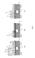
Figures 1 (a) to (k) a process flow according to an example embodiment of the present invention is depicted. - In
Figure 1(a) asubstrate 1 is provided. Active regions are formed with P-wells and N-wells as known in the art (not depicted). The active regions are electrically isolated from each other with isolation regions such as for example Shallow Trench Isolation (STI) structures as known in the art. An interfacial layer (101, not depicted) is formed, which typically comprises a silicon oxide. It can be a grown or deposited SiO2, and can have a thickness in between 0.1 to 2 nm depending on the targeted application. - A high-k dielectric layer or layer stack is provided on a main surface (e.g. front surface) of the substrate. The dielectric layer or
layer stack 3 can for instance comprise the interfacial silicon oxide, and/or a high-k dielectric, the latter for instance based on Hf. The high-k dielectric can for instance be or comprise a Hf oxide, HfSi oxide, or another doped Hf metal oxide. The thickness of the high-k dielectric can depend on the application, and can for instance be between 1 and 3 nm, although other thicknesses are not excluded. - In
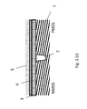
Figure 1(b) anetch stop layer 4 is provided on top of thedielectric layer 3. The functionality of this layer comprises stopping the wet etch of the metal layers of metal layer stacks (also called "metallic behaving layer") with the N or P type shifting element comprised in it. - The
etch stop layer 4 preferably satisfies some, preferably all, of the following criteria: - can be etched by reactive ion etching (RIE) for a gate etch;
- it is not etched by the wet etch chemistry used for the wet etch of the metallic behaving layer with the N or P type shifting element contained in it (eg. H2O2 , APM (NH4OH:H2O2:H2O mixture, also called SC-1) or SPM (H2SO4:H2O2 mixture), HCl.);
- provides sufficient conductivity in the used thickness range (for instance resistivity*thickness ≤ 10-7 Ωcm2).
- Possibly, the etch stop layer can constitute a moderate diffusion barrier, preferably at the temperature used for the diffusion anneal step. The etch stop layer can have a diffusion coefficient or diffusivity within the range of 1e-14 cm2/s to 5e-21 cm2/s, more preferably within the range of 1e-16cm2/s to 5e-20 cm2/s, even more preferably within the range of 1e-17cm2/s to 5e-19 cm2/s.
- The
etch stop layer 4 can be one layer but can be a multilayer (depicted as one layer), where the bottom layer provides the metallic behaving interface with the high-k dielectric layer, and the top layer can act as etch stop layer (and could be less metallic- behaving in nature). - The thickness of both layers is not restricted but the combined thickness is preferably in the range of 1 to 6 nm, more preferably in the range of 1 to 3 nm. For each layer the thickness is preferably in the range of 1 to 3 nm, more preferably within the range of 1 to 2 nm. In case a metal oxide is used as top layer its thickness is preferably smaller than the tunneling distance for electrons and holes (.preferably smaller than 2 nm)
- In case the
etch stop layer 4 is embodied by only one layer, it preferably shows the metallic behavior and should preferably act as an etch stop layer at the same time. - For instance, in case of a bi-layer, the top layer of the
etch stop layer 4 can for instance be made of or can comprise: more noble metals (like Ru, Pt and Ir), non etchable or less wet etchable metal nitrides that still behave metallic (e.g. TaN, HfN, NbN,MoN....), non or less wet etchable Metal oxides that behave metallic (e.g. RuOx , MoOx<=2,...), non or less wet etchable metal oxides that have a low band gap (e.g. Ta2O3, TaOx, Nb2O5, Sc2O3,....), non or less wet etchable metal silicide (metallic) (e.g. TiSix, TaSix, NiSix, CoSix, PtSix, ....). - The bottom layer of the
etch stop layer 4, in case of a bi-layer, preferably satisfies the regular criteria of a metal gate, known to the skilled person. It preferably demonstrates metallic behavior and the appropriate starting work function in absence of the shifting element. In that case it can for instance be made of or comprise any metal (e.g. W), metallic behaving metal Nitride (e.g. TiN, TaN, HfN, NbN,MoN....), metallic behaving oxide (e.g. RuOx , WOx, MoOx<=2,...) or Metal silicide (metallic) (e.g. TiSix, TaSix, NiSix, CoSix, PtSix, ....). - In case the
etch stop layer 4 is embodied by only one layer, the etch stop layer can for instance comprise or be made of any non wet etching metal (Pt, Ru, ....) or metallic behaving metal Nitride (e.g. TaN, HfN, NbN,MoN....), metallic behaving oxide (e.g. RuOx ,MoOx<=2,...) or Metal silicide (metallic) (e.g. TiSix, TaSix, NiSix, CoSix, PtSix, ....).
In case of the metal oxides, a low band gap is preferably required to provide sufficient electron and hole conduction through the thin metal oxide (tunneling or hopping based conduction are considered both to be appropriate), despite the dielectric nature of the layer. In a certain view, it acts as a (semi) transparent layer for the electrons and the holes. A low band gap preferably corresponds to a band gap smaller than 3 eV, or smaller than 2 eV, or smaller than 1 eV. - Examples of preferred
etch stop layers 4 are given below: - TaN (2-3 nm thick)
- a bilayer of TaN (2-3 nm thick)/TaO(2-3 nm thick)
- a bilayer of TiN (2-3 nm thick)/TaO(2-3 nm thick), where the TaO layer can for instance, but not only, be formed by air oxidation (e.g. 24 hours in ambient atmosphere) of a 2 nm deposited Ta layer.
- This is based on the following reasoning and observations.
- Many metals can be used above the etch stop layer, as work function-shifting element, but the preferred case are TiN based metals as TiN can be selectively etched by APM (H2O2 and SPM).
- Wet etch rate measurements in APM have shown:
- Etch rate (ER) TiN
- PVD TiN: 0.4 nm/s
- ALD TiN: 0.06 nm /s
- ER TaN (PVD TaN, with and without air break)
- 0.067 nm/s
- Selectivity to PVD TIN: 0.4/0.067 = 5.9 X
- ER Ta (PVD Ta no air break)
- 0.026 nm/s
- Selectivity to PVD TIN: 0.4/0.026 = 15 X
- ER Ta (PVD Ta with air break)
- 0.005 nm/s
- Selectivity to PVD TIN: 0.4/0.005 = 80 X
- Selectivity likely due to Ta2O3 formation (thickness unknown)
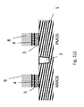
- In
Figure 1(c) , the first metal layer or firstmetal layer stack 5 is provided, comprising an N-type shifting element. - The first metal layer of first metal gate stack comprising the N-type shifting element can be for instance a TiN/Mg/TiN sandwich structure, Mg/TiN where the
etch stop layer 4 acts as bottom layer (etch stop layer/Mg/TiN), La or La2O3 capping or a TiN/La/TiN sandwich structure, or any other multi-layer stack that can provide a N-type work function by out-diffusion of dopant(s) through theetch stop layer 4 into the high-k dielectric layer. - The first metal layer of first metal gate stack comprising the N-type shifting element can for instance be composed of a matrix (metal, metal compound (nitride or oxide), dielectric (SiO2)) containing an additive element (shifting element) that allows shifting the work function towards the conduction (N-type shifter) band edge by diffusing it into or through the high-k gate dielectric stack (being the combination of the interfacial oxide and or the high-k itself).
- The additive element for N-type shifting can be a rare earth metal or rare earth metal oxide, or Mg and its oxide. It can also be an alkaline earth metal or its oxide.
The N-type shifting elements of the rare earth type can preferably be any or any combination of La, Gd, Tb, Er, Yb, Dy, Lu, Y, Yb, Sc.
The N-type shifting elements of the alkaline earth metal type can preferably be any or any combination of Mg, Sr. - In
Figure 1 (d) the first metal layer ormetal layer stack 5 is patterned. A part of thelayer 5 is removed by wet processing on the second predetermined area. An organic (for instance resist with or without BARC)mask 6 based wet etch of the N-type material (or stack) is performed.
In case the N-type material (or stack) is a metal or a metal nitride this wet etch can make use of H2O2, APM, SPM or another applicable wet chemistry.
In case the N-type material (or stack) is an oxide this wet etch can make use of a HF based wet chemistry.
Optionally, part or the whole N-type material (or stack) removal can be performed by RIE (only full dry removal in case of selectivity to the etch stop layer). -
Figure 1(e) illustrates the N-shifting elements out-diffusion ("drive-in" anneal) from thefirst metal layer 5 though theetch stop layer 4 into thedielectric layer 3 in a first predetermined area. - This optional drive-in anneal has to diffuse the N-type shifting element into or through the high-k gate dielectric stack (possibly being the combination of the interfacial oxide and the high-k layer).
- This step is optional and can advantageously be used when the subsequent drive-in anneal of P-type shifting elements is not sufficient on the N side, i.e. in the first predetermined area.
- The same applies in the "PMOS-first" embodiments wherein the order of the provisioning steps for the N-shifting and P-shifting elements is switched.
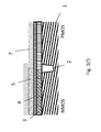
-
Figure 1(f) , the second metal layer or secondmetal layer stack 7 is provided, comprising a N-type shifting element. - This second metal layer or second
metal layer stack 7 can for instance be: - a capping layer such as Al or Al2O3 of e.g. 2nm thickness;
- a sandwich structure such as TiN/Al/TiN of e.g. 2 nm/2nm/2nm thickness;
- Al(or Al2O3)/TiN where the etch stop layer acts as bottom layer (etch stop layer/Al(or Al2O3)/TiN ),
- any other multi-layer stack that can provide a P-type work function by out-diffusion of dopant(s) through the
etch stop layer 4 into the high-k dielectric 3. - This second metal layer or second
metal layer stack 7 can be composed of a matrix (metal, metal compound (nitride or oxide), dielectric (SiO2)) containing an additive element that allows shifting the work function towards the silicon (or semiconductor substrate) valence (P-type shifter) band edge by diffusing it into or through the high-k gate dielectric stack (possibly being the combination of the interfacial oxide and the high-k dielectric). - The P-type shifting element can for instance be or comprise Al (for instance as Al or Al2O3).
-
Figure 1(g) illustrates the P-type shifting element out-diffusion anneal step ("drive-in anneal"). An anneal is performed to diffuse the N-type shifting element and the P-type shifting element through theetch stop layer 4 and into or through the high-k gate dielectric stack 3 (possibly being the combination of the interfacial oxide and or the high-k itself), in the respective areas. The anneal step will diffuse both the N and P-type shifting elements. - According to preferred embodiments, either the PMOS or NMOS side is processed first, in view of which sequence gives the best flexibility for controlling the dopant diffusion into the gate stack
-
Figure 1(h) illustrates the removal of the first and second metal layers or first and second metal layer stacks. A wet removal of the first or second metal layer or first or secondmetal layer stack etch stop layer 4 is performed.
In case the N- and P-type material (or stack) is a metal or a metal nitride this wet etch can for instance make use of H2O2, APM, SPM or another applicable wet chemistry.
In case the N-type material (or stack) is an oxide, this wet etch can for instance make use of HF based wet chemistry.
Optionally, part or the whole N and P- type material (or stack) etch can be removed by RIE (only full dry removal in case of selectivity to the etch stop layer). -
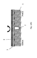
Figure 1(i) illustrates the deposition of agate capping layer 8. Thegate capping layer 8 for instance can be or comprise TiN (or any other metal or metallic behaving compound) and can further comprise for instance silicon. The capping layer can for instance comprise a first sublayer of TiN and a second sublayer of silicon. -
Figure 1(j) illustrates the gate patterning process. - The etch can be performed on NMOS and PMOS sides, whereby both sides have about the same gate height and materials, providing a symmetric gate technology on NMOS and PMOS. The formation of a foot due to a different or thicker metal on the N or P-side can thus be avoided. Such a foot (triangular-shaped edge of gate in its lower portion (
regions 3 + 4) can disadvantageously be formed when a non-homogeneous material stack is etched. This is a problem especially when different stack heights for NMOS and PMOS device are present. - It will be appreciated by the skilled person that according to embodiments of the present disclosure, the high-k dielectric layer or stack is protected from wet cleaning or plasma processing, up until the gate etch step.
-
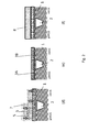
Figure 1(k) illustrates the final phase of the front end of line (FEOL) processing, whereby a MOSFET device is manufactured. Extension implants are provided (illustrated as dashed lines).Spacers 10 are formed. Source/Drain implants are performed (dashed lines). A silicidation process is performed inregions - In
Figures 2 (a) to (h) a process flow according to another example embodiment of the present invention is depicted, wherein no use is made of the etch stop layer. The process steps and device characteristics are further generally similar to those described in accordance withFig. 1 , but some constraints associated to the etch stop layer are not anymore an issue. This can result is some other material systems which can be used. It is expected that it is also easier to tune the work function according to this flow. - Note that the interfacial oxide layer (101) (also present in
Fig. 1 ) is explicitly shown in this flow. In this flow, high-k is though exposed to wet chemistry (e.g. in steps 2.b. and 2.e.), with associated yield and reliability issues.
Claims (13)
- A method for manufacturing a dual work function semiconductor device, the method comprising:- providing a substrate comprising a first predetermined area for producing a transistor of a first conduction type and a second predetermined area for producing a transistor of a second conduction type, the first conduction type being different from the second conduction type;- providing a dielectric layer on the substrate, said dielectric layer extending over both said first area and said second area;- providing a first metal layer or first metal layer stack comprising a first work function-shifting element on said dielectric layer in said first predetermined area;- providing a second metal layer or second metal layer stack comprising a second work function-shifting element on said first metal layer and said dielectric layer, in said first predetermined area and said second predetermined area respectively;- performing an anneal step adapted for driving diffusion of the first work function-shifting elements and the second work function-shifting elements into the dielectric layer;- removing said first metal layer or first metal layer stack and said second metal layer or second metal layer stack;- providing a third metal layer or third metal layer stack in said first predetermined area and said second predetermined area.
- Method according to claim 1, comprising an independent anneal step, for driving diffusion of the first work function-shifting elements into said dielectric layer, before depositing said second metal layer or second metal layer stack comprising said second work function-shifting element.
- Method according to claim 1 or 2, wherein the anneal step is such that it does not provide diffusion of said second work function-shifting element into said dielectric layer in said first predetermined area.
- Method according to any of the previous claims, further comprising providing an etch stop layer on said dielectric layer before depositing said first and said second metal layer or said first and said second metal layer stack, said etch stop layer not being etchable by an etchant adapted for etching said first metal layer or first metal layer stack and/or said second metal layer or second metal layer stack, and said etch stop layer being adapted for allowing the diffusion of said first work function-shifting elements and said second work function-shifting elements through it.
- Method according to claim 4, wherein said etch stop layer comprises any of or any combination of TaN, Ta, TaO or Ta2O3, TiN.
- Method according to claim 5, wherein said etch stop layer is embodied as a bilayer comprising a TaN layer and a TaO or Ta2O3 layer, or as a bi-layer comprising a TiN layer and a TaO or Ta2O3 layer.
- Method according to any of the previous claims, wherein said first metal layer or first metal layer stack, or said second metal or second metal layer stack comprises TiN/Mg/TiN, or Mg/TiN, La, La2O3, or TiN/La/TiN.
- Method according to any of the previous claims, wherein said first metal layer or first metal layer stack or said second metal layer or second metal layer stack comprises Aluminum.
- Method according to claim 8, said first metal layer or first metal layer stack or said second metal layer or second metal layer stack comprises Aluminum oxide covered with a layer of TiN or covered with a trilayer comprising TiN/Al/TiN.
- Method according to claim 4, wherein said etch stop layer has a thickness between 0.5 nm and 20 nm.
- Method according to any of the previous claims, wherein said substrate comprises an isolation area electrically isolating said first predetermined area from said second predetermined area, further comprising removing a portion of said dielectric layer, if present said etch stop layer, and said third metal layer or third metal layer stack at a location above said isolation region.
- Method according to any of the previous claims, wherein said dielectric layer comprises a high-k dielectric.
- Method according to claim 12, wherein said high-k dielectric comprises HfO2, HfSiOxide, HfSiN, ZrO2, or a doped Hf Metal Oxide.
Priority Applications (3)
| Application Number | Priority Date | Filing Date | Title |
|---|---|---|---|
| EP12187571.0A EP2717308A1 (en) | 2012-10-08 | 2012-10-08 | A method for manufacturing a dual work function semiconductor device |
| JP2013206863A JP6274805B2 (en) | 2012-10-08 | 2013-10-02 | Manufacturing method of dual work function semiconductor device |
| US14/047,849 US9245759B2 (en) | 2012-10-08 | 2013-10-07 | Method for manufacturing a dual work function semiconductor device |
Applications Claiming Priority (1)
| Application Number | Priority Date | Filing Date | Title |
|---|---|---|---|
| EP12187571.0A EP2717308A1 (en) | 2012-10-08 | 2012-10-08 | A method for manufacturing a dual work function semiconductor device |
Publications (1)
| Publication Number | Publication Date |
|---|---|
| EP2717308A1 true EP2717308A1 (en) | 2014-04-09 |
Family
ID=47010347
Family Applications (1)
| Application Number | Title | Priority Date | Filing Date |
|---|---|---|---|
| EP12187571.0A Withdrawn EP2717308A1 (en) | 2012-10-08 | 2012-10-08 | A method for manufacturing a dual work function semiconductor device |
Country Status (3)
| Country | Link |
|---|---|
| US (1) | US9245759B2 (en) |
| EP (1) | EP2717308A1 (en) |
| JP (1) | JP6274805B2 (en) |
Families Citing this family (5)
| Publication number | Priority date | Publication date | Assignee | Title |
|---|---|---|---|---|
| US9484427B2 (en) | 2014-07-01 | 2016-11-01 | Globalfoundries Inc. | Field effect transistors having multiple effective work functions |
| JP2016054250A (en) * | 2014-09-04 | 2016-04-14 | 豊田合成株式会社 | Semiconductor device and manufacturing method thereof |
| US9859392B2 (en) | 2015-09-21 | 2018-01-02 | Samsung Electronics Co., Ltd. | Integrated circuit device and method of manufacturing the same |
| KR20180091245A (en) | 2017-02-06 | 2018-08-16 | 삼성전자주식회사 | Semiconductor device and Method for fabricating the same |
| CN114765132A (en) * | 2021-01-11 | 2022-07-19 | 长鑫存储技术有限公司 | Semiconductor structure manufacturing method and semiconductor structure |
Citations (9)
| Publication number | Priority date | Publication date | Assignee | Title |
|---|---|---|---|---|
| US20090309165A1 (en) * | 2008-06-12 | 2009-12-17 | Hisashi Ogawa | Semiconductor device and method for manufacturing the same |
| US20100001348A1 (en) * | 2008-07-01 | 2010-01-07 | Riichirou Mitsuhashi | Semiconductor device and fabrication method for the same |
| US20100038729A1 (en) * | 2008-08-13 | 2010-02-18 | Renesas Technology Corp. | Method of manufacturing semiconductor device and semiconductor device |
| US20100197128A1 (en) * | 2009-02-04 | 2010-08-05 | Schaeffer James K | CMOS Integration with Metal Gate and Doped High-K Oxides |
| JP2010177265A (en) * | 2009-01-27 | 2010-08-12 | Fujitsu Semiconductor Ltd | Manufacturing method for semiconductor device |
| US20100279496A1 (en) * | 2009-04-30 | 2010-11-04 | Renesas Technology Corp. | Manufacturing method of semiconductor device |
| JP2010272596A (en) * | 2009-05-19 | 2010-12-02 | Renesas Electronics Corp | Method of manufacturing semiconductor device |
| US20100327365A1 (en) * | 2009-06-24 | 2010-12-30 | Renesas Electronics Corporation | Method of manufacturing semiconductor device and semiconductor device |
| JP2011029296A (en) * | 2009-07-23 | 2011-02-10 | Fujitsu Semiconductor Ltd | Method of manufacturing semiconductor-device and semiconductor device |
Family Cites Families (10)
| Publication number | Priority date | Publication date | Assignee | Title |
|---|---|---|---|---|
| US6794234B2 (en) * | 2002-01-30 | 2004-09-21 | The Regents Of The University Of California | Dual work function CMOS gate technology based on metal interdiffusion |
| US7291527B2 (en) * | 2005-09-07 | 2007-11-06 | Texas Instruments Incorporated | Work function control of metals |
| JP2009194352A (en) * | 2008-01-17 | 2009-08-27 | Toshiba Corp | Semiconductor device fabrication method |
| US20090286387A1 (en) * | 2008-05-16 | 2009-11-19 | Gilmer David C | Modulation of Tantalum-Based Electrode Workfunction |
| DE102009047310B4 (en) * | 2009-11-30 | 2013-06-06 | Globalfoundries Dresden Module One Limited Liability Company & Co. Kg | Work function setting in high ε gate stack for devices with different threshold voltages |
| US8343865B2 (en) * | 2010-01-21 | 2013-01-01 | Renesas Electronics Corporation | Semiconductor device having dual work function metal |
| US8643115B2 (en) * | 2011-01-14 | 2014-02-04 | International Business Machines Corporation | Structure and method of Tinv scaling for high κ metal gate technology |
| JP2012186259A (en) * | 2011-03-04 | 2012-09-27 | Renesas Electronics Corp | Semiconductor device manufacturing method and semiconductor device |
| JP5824661B2 (en) * | 2011-03-25 | 2015-11-25 | パナソニックIpマネジメント株式会社 | Semiconductor device and manufacturing method thereof |
| US8729637B2 (en) * | 2011-10-05 | 2014-05-20 | International Business Machines Corporation | Work function adjustment by carbon implant in semiconductor devices including gate structure |
-
2012
- 2012-10-08 EP EP12187571.0A patent/EP2717308A1/en not_active Withdrawn
-
2013
- 2013-10-02 JP JP2013206863A patent/JP6274805B2/en active Active
- 2013-10-07 US US14/047,849 patent/US9245759B2/en active Active
Patent Citations (9)
| Publication number | Priority date | Publication date | Assignee | Title |
|---|---|---|---|---|
| US20090309165A1 (en) * | 2008-06-12 | 2009-12-17 | Hisashi Ogawa | Semiconductor device and method for manufacturing the same |
| US20100001348A1 (en) * | 2008-07-01 | 2010-01-07 | Riichirou Mitsuhashi | Semiconductor device and fabrication method for the same |
| US20100038729A1 (en) * | 2008-08-13 | 2010-02-18 | Renesas Technology Corp. | Method of manufacturing semiconductor device and semiconductor device |
| JP2010177265A (en) * | 2009-01-27 | 2010-08-12 | Fujitsu Semiconductor Ltd | Manufacturing method for semiconductor device |
| US20100197128A1 (en) * | 2009-02-04 | 2010-08-05 | Schaeffer James K | CMOS Integration with Metal Gate and Doped High-K Oxides |
| US20100279496A1 (en) * | 2009-04-30 | 2010-11-04 | Renesas Technology Corp. | Manufacturing method of semiconductor device |
| JP2010272596A (en) * | 2009-05-19 | 2010-12-02 | Renesas Electronics Corp | Method of manufacturing semiconductor device |
| US20100327365A1 (en) * | 2009-06-24 | 2010-12-30 | Renesas Electronics Corporation | Method of manufacturing semiconductor device and semiconductor device |
| JP2011029296A (en) * | 2009-07-23 | 2011-02-10 | Fujitsu Semiconductor Ltd | Method of manufacturing semiconductor-device and semiconductor device |
Non-Patent Citations (1)
| Title |
|---|
| J. R. HAUSER; K. AHMED: "Characterization of Ultra-Thin Oxides Using Electrical C-V and I-V Measurements.", INTERNATIONAL CONFERENCE ON CHARACTERIZATION AND METROLOGY FOR ULSI TECHNOLOGY, 1998, pages 235 - 239 |
Also Published As
| Publication number | Publication date |
|---|---|
| JP6274805B2 (en) | 2018-02-07 |
| US9245759B2 (en) | 2016-01-26 |
| JP2014078708A (en) | 2014-05-01 |
| US20140106556A1 (en) | 2014-04-17 |
Similar Documents
| Publication | Publication Date | Title |
|---|---|---|
| US10424517B2 (en) | Method for manufacturing a dual work function semiconductor device and the semiconductor device made thereof | |
| EP2112687B1 (en) | Method for fabricating a dual workfunction semiconductor device and the device made thereof | |
| US8012827B2 (en) | Method for fabricating a dual workfunction semiconductor device and the device made thereof | |
| US8912607B2 (en) | Replacement metal gate structures providing independent control on work function and gate leakage current | |
| US8232154B2 (en) | Method for fabricating semiconductor device | |
| US7855134B2 (en) | Semiconductor device and manufacturing method of the same | |
| US7838356B2 (en) | Gate dielectric first replacement gate processes and integrated circuits therefrom | |
| US20080096383A1 (en) | Method of manufacturing a semiconductor device with multiple dielectrics | |
| US9018739B2 (en) | Semiconductor device and method of fabricating the same | |
| US20100181620A1 (en) | Structure and method for forming programmable high-k/metal gate memory device | |
| US20100109095A1 (en) | Method for fabricating a dual work function semiconductor device and the device made thereof | |
| JPWO2009072421A1 (en) | CMOS semiconductor device and manufacturing method thereof | |
| CN103426821B (en) | The method that semiconductor integrated circuit manufactures | |
| US20180277447A1 (en) | Method for manufacturing cmos structure | |
| US9245759B2 (en) | Method for manufacturing a dual work function semiconductor device | |
| US20100301429A1 (en) | Semiconductor device and method of manufacturing the same | |
| US10971397B2 (en) | Semiconductor device and method of fabricating the same | |
| EP2197028A1 (en) | Method for fabricating a dual workfunction semiconductor device and the device made thereof | |
| US20090224327A1 (en) | Plane mos and the method for making the same | |
| US7755145B2 (en) | Semiconductor device and manufacturing method thereof | |
| US20090039440A1 (en) | Semiconductor device and method of fabricating the same | |
| US10332804B2 (en) | Method for manufacturing CMOS structure | |
| JP2008117842A (en) | Semiconductor device, and method for manufacturing the same | |
| TWI488240B (en) | Method for fabricating semiconductor device |
Legal Events
| Date | Code | Title | Description |
|---|---|---|---|
| PUAI | Public reference made under article 153(3) epc to a published international application that has entered the european phase |
Free format text: ORIGINAL CODE: 0009012 |
|
| AK | Designated contracting states |
Kind code of ref document: A1 Designated state(s): AL AT BE BG CH CY CZ DE DK EE ES FI FR GB GR HR HU IE IS IT LI LT LU LV MC MK MT NL NO PL PT RO RS SE SI SK SM TR |
|
| AX | Request for extension of the european patent |
Extension state: BA ME |
|
| 17P | Request for examination filed |
Effective date: 20140923 |
|
| RBV | Designated contracting states (corrected) |
Designated state(s): AL AT BE BG CH CY CZ DE DK EE ES FI FR GB GR HR HU IE IS IT LI LT LU LV MC MK MT NL NO PL PT RO RS SE SI SK SM TR |
|
| 17Q | First examination report despatched |
Effective date: 20160316 |
|
| STAA | Information on the status of an ep patent application or granted ep patent |
Free format text: STATUS: THE APPLICATION IS DEEMED TO BE WITHDRAWN |
|
| 18D | Application deemed to be withdrawn |
Effective date: 20160927 |