JP5313424B2 - III-nitride based field effect transistor (FET) with reduced trapping and method of manufacturing the transistor - Google Patents
III-nitride based field effect transistor (FET) with reduced trapping and method of manufacturing the transistor Download PDFInfo
- Publication number
- JP5313424B2 JP5313424B2 JP2001557092A JP2001557092A JP5313424B2 JP 5313424 B2 JP5313424 B2 JP 5313424B2 JP 2001557092 A JP2001557092 A JP 2001557092A JP 2001557092 A JP2001557092 A JP 2001557092A JP 5313424 B2 JP5313424 B2 JP 5313424B2
- Authority
- JP
- Japan
- Prior art keywords
- fet
- layer
- barrier layer
- electron
- donor
- Prior art date
- Legal status (The legal status is an assumption and is not a legal conclusion. Google has not performed a legal analysis and makes no representation as to the accuracy of the status listed.)
- Expired - Lifetime
Links
- 238000004519 manufacturing process Methods 0.000 title claims abstract description 8
- 230000005669 field effect Effects 0.000 title claims abstract description 5
- 238000004544 sputter deposition Methods 0.000 claims abstract description 22
- 238000000034 method Methods 0.000 claims abstract description 14
- 150000004767 nitrides Chemical class 0.000 claims abstract description 6
- 230000004888 barrier function Effects 0.000 claims description 42
- 239000000758 substrate Substances 0.000 claims description 16
- 239000000463 material Substances 0.000 claims description 14
- HBMJWWWQQXIZIP-UHFFFAOYSA-N silicon carbide Chemical compound [Si+]#[C-] HBMJWWWQQXIZIP-UHFFFAOYSA-N 0.000 claims description 12
- 229910010271 silicon carbide Inorganic materials 0.000 claims description 11
- 239000004065 semiconductor Substances 0.000 claims description 10
- 229910052710 silicon Inorganic materials 0.000 claims description 7
- 239000010703 silicon Substances 0.000 claims description 7
- 229910052581 Si3N4 Inorganic materials 0.000 claims description 6
- 239000002019 doping agent Substances 0.000 claims description 6
- HQVNEWCFYHHQES-UHFFFAOYSA-N silicon nitride Chemical compound N12[Si]34N5[Si]62N3[Si]51N64 HQVNEWCFYHHQES-UHFFFAOYSA-N 0.000 claims description 6
- 229910052594 sapphire Inorganic materials 0.000 claims description 3
- 239000010980 sapphire Substances 0.000 claims description 3
- 230000005533 two-dimensional electron gas Effects 0.000 claims description 3
- 238000001816 cooling Methods 0.000 claims 1
- 238000013022 venting Methods 0.000 claims 1
- 229910002704 AlGaN Inorganic materials 0.000 abstract description 19
- 230000004044 response Effects 0.000 abstract description 4
- 238000010586 diagram Methods 0.000 description 12
- JBRZTFJDHDCESZ-UHFFFAOYSA-N AsGa Chemical compound [As]#[Ga] JBRZTFJDHDCESZ-UHFFFAOYSA-N 0.000 description 7
- XKRFYHLGVUSROY-UHFFFAOYSA-N Argon Chemical compound [Ar] XKRFYHLGVUSROY-UHFFFAOYSA-N 0.000 description 6
- IJGRMHOSHXDMSA-UHFFFAOYSA-N Atomic nitrogen Chemical compound N#N IJGRMHOSHXDMSA-UHFFFAOYSA-N 0.000 description 6
- 229910001218 Gallium arsenide Inorganic materials 0.000 description 6
- PXHVJJICTQNCMI-UHFFFAOYSA-N Nickel Chemical compound [Ni] PXHVJJICTQNCMI-UHFFFAOYSA-N 0.000 description 6
- XUIMIQQOPSSXEZ-UHFFFAOYSA-N Silicon Chemical compound [Si] XUIMIQQOPSSXEZ-UHFFFAOYSA-N 0.000 description 6
- 238000000151 deposition Methods 0.000 description 6
- 229910052782 aluminium Inorganic materials 0.000 description 5
- XAGFODPZIPBFFR-UHFFFAOYSA-N aluminium Chemical compound [Al] XAGFODPZIPBFFR-UHFFFAOYSA-N 0.000 description 5
- 230000003321 amplification Effects 0.000 description 4
- 239000007789 gas Substances 0.000 description 4
- 230000007935 neutral effect Effects 0.000 description 4
- 238000003199 nucleic acid amplification method Methods 0.000 description 4
- 229910052786 argon Inorganic materials 0.000 description 3
- 239000011248 coating agent Substances 0.000 description 3
- 238000000576 coating method Methods 0.000 description 3
- 229910052759 nickel Inorganic materials 0.000 description 3
- 230000008569 process Effects 0.000 description 3
- 239000007787 solid Substances 0.000 description 3
- 229910001069 Ti alloy Inorganic materials 0.000 description 2
- RTAQQCXQSZGOHL-UHFFFAOYSA-N Titanium Chemical compound [Ti] RTAQQCXQSZGOHL-UHFFFAOYSA-N 0.000 description 2
- 229910045601 alloy Inorganic materials 0.000 description 2
- 239000000956 alloy Substances 0.000 description 2
- 238000000137 annealing Methods 0.000 description 2
- 125000004429 atom Chemical group 0.000 description 2
- 230000015572 biosynthetic process Effects 0.000 description 2
- 230000015556 catabolic process Effects 0.000 description 2
- 150000001875 compounds Chemical class 0.000 description 2
- 239000004020 conductor Substances 0.000 description 2
- 239000013078 crystal Substances 0.000 description 2
- 230000007423 decrease Effects 0.000 description 2
- 229910001873 dinitrogen Inorganic materials 0.000 description 2
- 238000005516 engineering process Methods 0.000 description 2
- 239000012535 impurity Substances 0.000 description 2
- 239000011261 inert gas Substances 0.000 description 2
- 150000002500 ions Chemical class 0.000 description 2
- 229910052751 metal Inorganic materials 0.000 description 2
- 239000002184 metal Substances 0.000 description 2
- 229910052757 nitrogen Inorganic materials 0.000 description 2
- BASFCYQUMIYNBI-UHFFFAOYSA-N platinum Chemical compound [Pt] BASFCYQUMIYNBI-UHFFFAOYSA-N 0.000 description 2
- 229910052719 titanium Inorganic materials 0.000 description 2
- 239000010936 titanium Substances 0.000 description 2
- 230000007704 transition Effects 0.000 description 2
- ZXEYZECDXFPJRJ-UHFFFAOYSA-N $l^{3}-silane;platinum Chemical compound [SiH3].[Pt] ZXEYZECDXFPJRJ-UHFFFAOYSA-N 0.000 description 1
- VYZAMTAEIAYCRO-UHFFFAOYSA-N Chromium Chemical compound [Cr] VYZAMTAEIAYCRO-UHFFFAOYSA-N 0.000 description 1
- GYHNNYVSQQEPJS-UHFFFAOYSA-N Gallium Chemical compound [Ga] GYHNNYVSQQEPJS-UHFFFAOYSA-N 0.000 description 1
- UFHFLCQGNIYNRP-UHFFFAOYSA-N Hydrogen Chemical compound [H][H] UFHFLCQGNIYNRP-UHFFFAOYSA-N 0.000 description 1
- 229910001080 W alloy Inorganic materials 0.000 description 1
- 230000004913 activation Effects 0.000 description 1
- 239000000969 carrier Substances 0.000 description 1
- 230000010267 cellular communication Effects 0.000 description 1
- 238000005229 chemical vapour deposition Methods 0.000 description 1
- 229910052804 chromium Inorganic materials 0.000 description 1
- 239000011651 chromium Substances 0.000 description 1
- 238000004891 communication Methods 0.000 description 1
- 238000011109 contamination Methods 0.000 description 1
- PMHQVHHXPFUNSP-UHFFFAOYSA-M copper(1+);methylsulfanylmethane;bromide Chemical compound Br[Cu].CSC PMHQVHHXPFUNSP-UHFFFAOYSA-M 0.000 description 1
- 230000007547 defect Effects 0.000 description 1
- 230000008021 deposition Effects 0.000 description 1
- 238000011161 development Methods 0.000 description 1
- 239000003989 dielectric material Substances 0.000 description 1
- 238000004870 electrical engineering Methods 0.000 description 1
- 239000003574 free electron Substances 0.000 description 1
- 229910052733 gallium Inorganic materials 0.000 description 1
- PCHJSUWPFVWCPO-UHFFFAOYSA-N gold Chemical compound [Au] PCHJSUWPFVWCPO-UHFFFAOYSA-N 0.000 description 1
- 229910052737 gold Inorganic materials 0.000 description 1
- 239000010931 gold Substances 0.000 description 1
- 239000001257 hydrogen Substances 0.000 description 1
- 229910052739 hydrogen Inorganic materials 0.000 description 1
- 125000004435 hydrogen atom Chemical group [H]* 0.000 description 1
- 229910052738 indium Inorganic materials 0.000 description 1
- APFVFJFRJDLVQX-UHFFFAOYSA-N indium atom Chemical compound [In] APFVFJFRJDLVQX-UHFFFAOYSA-N 0.000 description 1
- 238000009413 insulation Methods 0.000 description 1
- 238000002955 isolation Methods 0.000 description 1
- 230000007246 mechanism Effects 0.000 description 1
- 230000008018 melting Effects 0.000 description 1
- 238000002844 melting Methods 0.000 description 1
- TWNQGVIAIRXVLR-UHFFFAOYSA-N oxo(oxoalumanyloxy)alumane Chemical compound O=[Al]O[Al]=O TWNQGVIAIRXVLR-UHFFFAOYSA-N 0.000 description 1
- 230000003071 parasitic effect Effects 0.000 description 1
- 238000002161 passivation Methods 0.000 description 1
- 230000000737 periodic effect Effects 0.000 description 1
- 238000000623 plasma-assisted chemical vapour deposition Methods 0.000 description 1
- 229910052697 platinum Inorganic materials 0.000 description 1
- 229910021339 platinum silicide Inorganic materials 0.000 description 1
- 238000005086 pumping Methods 0.000 description 1
- 238000011160 research Methods 0.000 description 1
- 239000010409 thin film Substances 0.000 description 1
- 238000012546 transfer Methods 0.000 description 1
- 238000003949 trap density measurement Methods 0.000 description 1
- WFKWXMTUELFFGS-UHFFFAOYSA-N tungsten Chemical compound [W] WFKWXMTUELFFGS-UHFFFAOYSA-N 0.000 description 1
- 239000010937 tungsten Substances 0.000 description 1
- 238000005406 washing Methods 0.000 description 1
Images


Classifications
-
- H—ELECTRICITY
- H01—ELECTRIC ELEMENTS
- H01L—SEMICONDUCTOR DEVICES NOT COVERED BY CLASS H10
- H01L29/00—Semiconductor devices adapted for rectifying, amplifying, oscillating or switching, or capacitors or resistors with at least one potential-jump barrier or surface barrier, e.g. PN junction depletion layer or carrier concentration layer; Details of semiconductor bodies or of electrodes thereof ; Multistep manufacturing processes therefor
- H01L29/66—Types of semiconductor device ; Multistep manufacturing processes therefor
- H01L29/68—Types of semiconductor device ; Multistep manufacturing processes therefor controllable by only the electric current supplied, or only the electric potential applied, to an electrode which does not carry the current to be rectified, amplified or switched
- H01L29/76—Unipolar devices, e.g. field effect transistors
- H01L29/772—Field effect transistors
- H01L29/778—Field effect transistors with two-dimensional charge carrier gas channel, e.g. HEMT ; with two-dimensional charge-carrier layer formed at a heterojunction interface
-
- H—ELECTRICITY
- H01—ELECTRIC ELEMENTS
- H01L—SEMICONDUCTOR DEVICES NOT COVERED BY CLASS H10
- H01L29/00—Semiconductor devices adapted for rectifying, amplifying, oscillating or switching, or capacitors or resistors with at least one potential-jump barrier or surface barrier, e.g. PN junction depletion layer or carrier concentration layer; Details of semiconductor bodies or of electrodes thereof ; Multistep manufacturing processes therefor
- H01L29/66—Types of semiconductor device ; Multistep manufacturing processes therefor
- H01L29/66007—Multistep manufacturing processes
- H01L29/66075—Multistep manufacturing processes of devices having semiconductor bodies comprising group 14 or group 13/15 materials
- H01L29/66227—Multistep manufacturing processes of devices having semiconductor bodies comprising group 14 or group 13/15 materials the devices being controllable only by the electric current supplied or the electric potential applied, to an electrode which does not carry the current to be rectified, amplified or switched, e.g. three-terminal devices
- H01L29/66409—Unipolar field-effect transistors
- H01L29/66848—Unipolar field-effect transistors with a Schottky gate, i.e. MESFET
- H01L29/66856—Unipolar field-effect transistors with a Schottky gate, i.e. MESFET with an active layer made of a group 13/15 material
- H01L29/66863—Lateral single gate transistors
-
- H—ELECTRICITY
- H01—ELECTRIC ELEMENTS
- H01L—SEMICONDUCTOR DEVICES NOT COVERED BY CLASS H10
- H01L29/00—Semiconductor devices adapted for rectifying, amplifying, oscillating or switching, or capacitors or resistors with at least one potential-jump barrier or surface barrier, e.g. PN junction depletion layer or carrier concentration layer; Details of semiconductor bodies or of electrodes thereof ; Multistep manufacturing processes therefor
- H01L29/66—Types of semiconductor device ; Multistep manufacturing processes therefor
- H01L29/66007—Multistep manufacturing processes
- H01L29/66075—Multistep manufacturing processes of devices having semiconductor bodies comprising group 14 or group 13/15 materials
- H01L29/66227—Multistep manufacturing processes of devices having semiconductor bodies comprising group 14 or group 13/15 materials the devices being controllable only by the electric current supplied or the electric potential applied, to an electrode which does not carry the current to be rectified, amplified or switched, e.g. three-terminal devices
- H01L29/66409—Unipolar field-effect transistors
- H01L29/66446—Unipolar field-effect transistors with an active layer made of a group 13/15 material, e.g. group 13/15 velocity modulation transistor [VMT], group 13/15 negative resistance FET [NERFET]
- H01L29/66462—Unipolar field-effect transistors with an active layer made of a group 13/15 material, e.g. group 13/15 velocity modulation transistor [VMT], group 13/15 negative resistance FET [NERFET] with a heterojunction interface channel or gate, e.g. HFET, HIGFET, SISFET, HJFET, HEMT
-
- H—ELECTRICITY
- H01—ELECTRIC ELEMENTS
- H01L—SEMICONDUCTOR DEVICES NOT COVERED BY CLASS H10
- H01L29/00—Semiconductor devices adapted for rectifying, amplifying, oscillating or switching, or capacitors or resistors with at least one potential-jump barrier or surface barrier, e.g. PN junction depletion layer or carrier concentration layer; Details of semiconductor bodies or of electrodes thereof ; Multistep manufacturing processes therefor
- H01L29/66—Types of semiconductor device ; Multistep manufacturing processes therefor
- H01L29/68—Types of semiconductor device ; Multistep manufacturing processes therefor controllable by only the electric current supplied, or only the electric potential applied, to an electrode which does not carry the current to be rectified, amplified or switched
- H01L29/76—Unipolar devices, e.g. field effect transistors
- H01L29/772—Field effect transistors
- H01L29/778—Field effect transistors with two-dimensional charge carrier gas channel, e.g. HEMT ; with two-dimensional charge-carrier layer formed at a heterojunction interface
- H01L29/7782—Field effect transistors with two-dimensional charge carrier gas channel, e.g. HEMT ; with two-dimensional charge-carrier layer formed at a heterojunction interface with confinement of carriers by at least two heterojunctions, e.g. DHHEMT, quantum well HEMT, DHMODFET
- H01L29/7783—Field effect transistors with two-dimensional charge carrier gas channel, e.g. HEMT ; with two-dimensional charge-carrier layer formed at a heterojunction interface with confinement of carriers by at least two heterojunctions, e.g. DHHEMT, quantum well HEMT, DHMODFET using III-V semiconductor material
-
- H—ELECTRICITY
- H01—ELECTRIC ELEMENTS
- H01L—SEMICONDUCTOR DEVICES NOT COVERED BY CLASS H10
- H01L23/00—Details of semiconductor or other solid state devices
- H01L23/28—Encapsulations, e.g. encapsulating layers, coatings, e.g. for protection
- H01L23/29—Encapsulations, e.g. encapsulating layers, coatings, e.g. for protection characterised by the material, e.g. carbon
- H01L23/291—Oxides or nitrides or carbides, e.g. ceramics, glass
-
- H—ELECTRICITY
- H01—ELECTRIC ELEMENTS
- H01L—SEMICONDUCTOR DEVICES NOT COVERED BY CLASS H10
- H01L29/00—Semiconductor devices adapted for rectifying, amplifying, oscillating or switching, or capacitors or resistors with at least one potential-jump barrier or surface barrier, e.g. PN junction depletion layer or carrier concentration layer; Details of semiconductor bodies or of electrodes thereof ; Multistep manufacturing processes therefor
- H01L29/02—Semiconductor bodies ; Multistep manufacturing processes therefor
- H01L29/12—Semiconductor bodies ; Multistep manufacturing processes therefor characterised by the materials of which they are formed
- H01L29/20—Semiconductor bodies ; Multistep manufacturing processes therefor characterised by the materials of which they are formed including, apart from doping materials or other impurities, only AIIIBV compounds
- H01L29/2003—Nitride compounds
-
- H—ELECTRICITY
- H01—ELECTRIC ELEMENTS
- H01L—SEMICONDUCTOR DEVICES NOT COVERED BY CLASS H10
- H01L2924/00—Indexing scheme for arrangements or methods for connecting or disconnecting semiconductor or solid-state bodies as covered by H01L24/00
- H01L2924/0001—Technical content checked by a classifier
- H01L2924/0002—Not covered by any one of groups H01L24/00, H01L24/00 and H01L2224/00
Landscapes
- Engineering & Computer Science (AREA)
- Power Engineering (AREA)
- Microelectronics & Electronic Packaging (AREA)
- Ceramic Engineering (AREA)
- Condensed Matter Physics & Semiconductors (AREA)
- General Physics & Mathematics (AREA)
- Physics & Mathematics (AREA)
- Computer Hardware Design (AREA)
- Manufacturing & Machinery (AREA)
- Chemical & Material Sciences (AREA)
- Materials Engineering (AREA)
- Junction Field-Effect Transistors (AREA)
- Semiconductor Lasers (AREA)
Abstract
Description
本出願は、2000年2月4日出願のWu他による米国仮出願一連番号第60/180,435号に基づく優先権を主張するものである。 This application claims priority from US Provisional Application Serial No. 60 / 180,435, filed February 4, 2000 by Wu et al.
(発明の背景)
(発明の分野)
本発明は、高周波のソリッドステートトランジスタ(solid state transistor)に関し、より詳しくは、III族窒化物ベースの電界効果トランジスタおよび高電子移動度トランジスタに関する。(Background of the Invention)
(Field of Invention)
The present invention relates to high frequency solid state transistors, and more particularly to III-nitride based field effect transistors and high electron mobility transistors.
(関連技術の説明)
マイクロ波システムは、一般に、ソリッドステートトランジスタを増幅器および発信器として使用しており、それにより、システムサイズ(system size)を著しく小さくし、信頼性を増大させた。拡大するマイクロ波システムに対処するためには、その動作周波数および動作電力を増すことが重要である。周波数信号が高いほどより多くの情報(帯域幅)を伝達することができ、非常に高い利得を持つより小さいアンテナが可能となり、解像度の改良されたレーダを提供する。(Description of related technology)
Microwave systems generally use solid state transistors as amplifiers and transmitters, thereby significantly reducing system size and increasing reliability. In order to cope with the growing microwave system, it is important to increase its operating frequency and operating power. The higher the frequency signal, the more information (bandwidth) can be transmitted, allowing a smaller antenna with very high gain, providing a radar with improved resolution.
電界効果トランジスタ(FET)および高電子移動度トランジスタ(HEMT)は、一般タイプのソリッドステートトランジスタであって、シリコン(Si)または砒化ガリウム(GaAs)等の半導体材料から作られる。Siの1つの不都合は、それが低い電子移動度(約1450cm2/V−s)を持ち、それによって高いソース(source)抵抗を生むことである。この抵抗のため、そうでなければSiに基づくFETおよびHEMTから得ることが可能な高性能の利得がひどく低下される。[CRC Press,The Electrical Engineering Handbook,Second Edition,Dorf,p.994,(1997)]Field effect transistors (FETs) and high electron mobility transistors (HEMTs) are common types of solid state transistors made from semiconductor materials such as silicon (Si) or gallium arsenide (GaAs). One disadvantage of Si is that it has a low electron mobility (about 1450 cm 2 / V-s), thereby producing a high source resistance. This resistance severely reduces the high performance gains that would otherwise be obtainable from Si-based FETs and HEMTs. [CRC Press, The Electrical Engineering Handbook, Second Edition, Dorf, p. 994, (1997)]
GaAsもまたFETおよびHEMTに用いる一般的な材料であり、民間用および軍事用レーダ、ハンドセットセルラー(handset cellular)通信、および、衛星通信における信号増幅の標準となっている。GaAsは、Siより高い電子移動度(約6000cm2/V−s)および低いソース抵抗を持っており、そのことが、GaAsベースのデバイスがより高い周波数で機能することを可能にしている。しかしながら、GaAsは比較的小さいバンドギャップ(室温で1.42eV)および比較的小さい降伏電圧(breakdown voltage)を有しており、そのことが、GaAsベースのFETおよびHEMTが高周波数において高い電力を提供することを妨げる。GaAs is also a common material used in FETs and HEMTs and has become the standard for signal amplification in civil and military radar, handset cellular communications, and satellite communications. GaAs has a higher electron mobility (approximately 6000 cm 2 / V-s) and lower source resistance than Si, which allows GaAs-based devices to function at higher frequencies. However, GaAs has a relatively small band gap (1.42 eV at room temperature) and a relatively small breakdown voltage, which makes GaAs-based FETs and HEMTs provide high power at high frequencies. Prevent you from doing.
GaN/AlGaN半導体材料の製造における改良は、GaN/AlGaNベースのFETおよびHEMTの開発に重点が絞られてきた。これらのデバイスは、高い降伏電界、広いバンドギャップ(室温のGaNで3.36eV)、大きな伝導帯オフセット(offset)、高い飽和電子ドリフト速度等を含む材料特性の独特の組合せによって大量の電力を発生することができる。同じ周波数で作動させて、同じ大きさのGaN増幅器が、GaAs増幅器の電力の10倍まで生ずることができる。 Improvements in the manufacture of GaN / AlGaN semiconductor materials have focused on the development of GaN / AlGaN based FETs and HEMTs. These devices generate large amounts of power through a unique combination of material properties including high breakdown field, wide band gap (3.36 eV for room temperature GaN), large conduction band offset, high saturation electron drift velocity, etc. can do. Operating at the same frequency, GaN amplifiers of the same magnitude can be produced up to 10 times the power of GaAs amplifiers.
米国特許第5,192,987号(Khan他)には、バッファ(buffer)および基板上に成長させたGaN/AlGaNベースのHEMTおよびそれを製造する方法が記載されている。Gaska等の「High−Temperature Performance of AlGaN/GaN HFET′s on SiC Substrates」、IEEE Electron Device Letters,Vol.18,No 10、1997年10月、492頁、および、Ping等の「DC and Microwave Performance of High Current AlGaN Hetero structure Field Effect Transistors Grown on P−type SiC Substrates」、IEEE Electron Device Letters,Vol.19,No.2、1998年2月、54頁には、他のHEMTが記載されている。これらのデバイスのいくつかは、67ギガヘルツもの高さの利得帯域幅積(fT)(K.Chu等、WOCSEMMAD,Montery,CA,1998年2月)、および、10GHzにおいて最大2.84W/mmまでの高い出力密度(G.Sullivan等の「High Power 10−GHz Operation of AlGaN HFET′s in Insulating SiC」、IEEE Electron Device Letters,Vol.19,No.6、1998年6月、198頁、および、Wu等のIEEE Electron Device Letters,Volume 19,No.2、1998年2月、50頁)を示した。US Pat. No. 5,192,987 (Khan et al.) Describes a GaN / AlGaN based HEMT grown on a buffer and substrate and a method of manufacturing the same. Gaska et al., “High-Temperature Performance of AlGaN / GaN HFET's on SiC Substrates”, IEEE Electron Devices Letters, Vol. 18,
これらの進歩にもかかわらず、GaN/AlGaNベースのFETおよびHEMTは、高い効率と高い利得を有するマイクロ波出力全体の際立った量を生み出すことはできていない。それらは直流(DC)ゲートドライブでは際立った電力利得を生ずるが、ミリヘルツから数キロヘルツというわずかの周波数の増加により、それらの増幅は著しく低下する。 Despite these advances, GaN / AlGaN based FETs and HEMTs have not been able to produce a significant amount of overall microwave output with high efficiency and high gain. They produce significant power gain in direct current (DC) gate drives, but their amplification is significantly reduced by a slight increase in frequency from millihertz to several kilohertz.
交流(AC)増幅と直流(DC)増幅の間の差は、デバイスのチャネル(channel)内の表面トラップ(trap)によって主として引き起こされるものと思われる。用語はいくぶんさまざまであるが、1つのタイプのキャリアを捕捉した後、最も確率の高い次の事象が再励起である場合、不純物または欠陥の中心をトラッピングセンタ(または単にトラップ)というのが一般的である。一般に、バンドギャップの深いところに位置するトラッピングの準位では、価電子帯の伝導の近くに位置する他の準位よりトラップしたキャリアを開放するのが遅くなる。これは、トラップした電子をバンドギャップの中央付近の中心から伝導帯に再励起させるために要するエネルギーが、電子をより近い準位から伝導帯に再励起させるために要するエネルギーと比較して増えるためである。 The difference between alternating current (AC) and direct current (DC) amplification appears to be mainly caused by surface traps in the device channel. The terminology is somewhat different, but after capturing one type of carrier, if the most probable next event is re-excitation, it is common to refer to the center of the impurity or defect as a trapping center (or simply trap) It is. In general, trapping levels located deep in the band gap are slower to release trapped carriers than other levels located near the valence band conduction. This is because the energy required to re-excited trapped electrons from the center near the center of the band gap to the conduction band increases compared to the energy required to re-excited electrons from the closer level to the conduction band. It is.
AlXGa1-XN(X=0〜1)は、0.7から1.8eV(Xに依存する)の範囲の活性化エネルギーを有する極度のドナー状態にあるトラップを有するトランジスタのチャネル電荷に匹敵する表面トラップ密度を有している。FETおよびHEMTが作動する間、そのトラップがチャネル電子を捕らえる。トラッピングの遅れおよび深いところのトラッピングプロセスは、トランジスタの速度を落とし、それによってマイクロ波の周波数における出力性能を大きく低下させる。Al X Ga 1-X N (X = 0 to 1) is the channel charge of a transistor with a trap in the extreme donor state with an activation energy in the range of 0.7 to 1.8 eV (depending on X). The surface trap density is comparable to While the FET and HEMT are operating, their traps capture channel electrons. The trapping delay and deep trapping process slows down the transistor, thereby greatly reducing the output performance at microwave frequencies.
(発明の概要)
本発明は、好ましくは、GaN/AlGaNから形成され交流ゲートドライブに応答する改良された増幅特性を示すIII族窒化物ベースの改良されたFETおよびHEMTを提供する。また、本発明は、その新規なGaN/AlGaNのFETおよびHEMTを製造する新規な方法を提供する。(Summary of Invention)
The present invention provides improved III-nitride based FETs and HEMTs that are preferably made of GaN / AlGaN and exhibit improved amplification characteristics in response to an alternating gate drive. The present invention also provides a novel method for fabricating the novel GaN / AlGaN FETs and HEMTs.
その新規なFETは、比抵抗が高い非伝導層上にバリア層を含む。ソース、ドレイン、および、ゲートのコンタクトが、それぞれそのバリア層と接触して含まれている。電子ドナー層がそのバリア層表面上のコンタクトの間に形成されており、そのドナー層は、好ましくは、高い割合のドナー電子を持つ誘電層である。 The novel FET includes a barrier layer on a non-conductive layer having a high specific resistance. Source, drain, and gate contacts are each included in contact with the barrier layer. An electron donor layer is formed between the contacts on the barrier layer surface, and the donor layer is preferably a dielectric layer with a high proportion of donor electrons.
新規なHEMTについていえば、そのバリア層は、非伝導層より幅広のバンドギャップを有しており、その結果、バリア層と非伝導層が接合する所に二次元電子ガス(2DEG)を形成する。その2DEGは、高濃度の電子を有しており、拡大されたデバイス相互コンダクタンスを提供する。この新規のHEMTは、FETの伝導チャネル(conducting channel)上のものと同様のコンタクトを有しており、同様の誘電層がHEMTの伝導チャネル上に含まれる。 For the new HEMT, the barrier layer has a wider band gap than the non-conductive layer, resulting in the formation of a two-dimensional electron gas (2DEG) where the barrier layer and non-conductive layer join. . The 2DEG has a high concentration of electrons and provides expanded device transconductance. The new HEMT has contacts similar to those on the conducting channel of the FET, and a similar dielectric layer is included on the conducting channel of the HEMT.
それぞれのデバイスにおいて、バリア層は、プラスに帯電している表面トラップを有しているものと思われる。また、誘電層のドナー電子が、デバイスのバリア層に移動し、その表面トラップを充満するものと思われる。これによってそれらが中性となるようにし、それらが自由電子を捕捉することを防ぐ。また、新規の誘電コーティング(coating)も、デバイスのゲートのない領域のシート(sheet)電子密度を増し、望ましくない不動態化、不純物および取り扱い中の損傷からデバイスを保護する。 In each device, the barrier layer appears to have positively charged surface traps. It also appears that the donor electrons in the dielectric layer migrate to the device barrier layer and fill its surface traps. This makes them neutral and prevents them from trapping free electrons. The novel dielectric coating also increases the sheet electron density in the device's gate-free area and protects the device from unwanted passivation, impurities and damage during handling.
本発明は、また、その新規なGaNのFETまたはHEMTを製造する方法を提供する。その新規な方法は、スパッタリング技術に依存するものであり、伝導チャネル表面の損傷は殆んど起こらない。それはまた、誘電層とチャネル表面の間の強くて安定した結合を提供する。 The present invention also provides a method of manufacturing the novel GaN FET or HEMT. The new method relies on sputtering technology and causes little damage to the conduction channel surface. It also provides a strong and stable bond between the dielectric layer and the channel surface.
本発明のこれらおよびさらなる特徴および利点は、添付した図面を伴う次の詳細な説明から、当技術分野の熟練者には明らかとなろう。 These and further features and advantages of the present invention will be apparent to those skilled in the art from the following detailed description, taken in conjunction with the accompanying drawings.
(発明の詳細な説明)
(新規GaN/AlGaNのFETおよびHEMT)
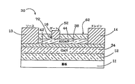
図1は、本発明に従って組み立てた新規なIII族窒化物ベースのFET10を示す。それは、サファイア(Al2O3)または炭化ケイ素(SiC)のいずれかであり得る基板11を含み、好ましい基板は、4Hポリタイプの炭化ケイ素である。3C、6Hおよび15Rポリタイプを含む他のポリタイプの炭化ケイ素もまた使用することができる。AlxGa1-xNバッファ層12(ただし、xは0と1の間)が基板11の上にあり、FET10の炭化ケイ素基板とその他のものとの間の適切な結晶構造の遷移(crystal structure transition)を提供する。(Detailed description of the invention)
(New GaN / AlGaN FET and HEMT)
FIG. 1 shows a novel III-nitride based FET 10 constructed in accordance with the present invention. It includes a
炭化ケイ素は、III族窒化物に対して、サファイアよりはるかに近い結晶格子整合を有しており、より高い品質のIII族窒化物薄膜をもたらす。炭化ケイ素はまた、非常に高い熱伝導性を有しており、そのため炭化ケイ素上のIII族窒化物デバイスの全出力能力は、(サファイア上に形成したデバイスの場合よくあるように)基板の熱散逸によって制限されない。また、炭化ケイ素基板の入手のし易さがデバイスを分離する余地および低減された寄生キャパシタンス(capacitance)を提供し、デバイスの工業化を可能にする。SiC基板は、ノースカロライナ州ダラムのCree Research,Inc.から入手でき、それらを製造する方法は、科学文献ならびに米国特許再発行特許明細書第34,861号、米国特許第4,946,547号、同第5,200,022号に明らかにされている。 Silicon carbide has a crystal lattice match much closer to sapphire than group III nitride, resulting in higher quality group III nitride thin films. Silicon carbide also has a very high thermal conductivity, so that the total power capability of a III-nitride device on silicon carbide is the thermal power of the substrate (as is often the case with devices formed on sapphire). Not limited by dissipation. Also, the availability of silicon carbide substrates provides room for device isolation and reduced parasitic capacitance, enabling device industrialization. The SiC substrate is available from Cree Research, Inc. of Durham, North Carolina. And methods for producing them are disclosed in the scientific literature as well as in U.S. Patent Reissue Patent Specification No. 34,861, U.S. Pat. Nos. 4,946,547 and 5,200,022. Yes.
III族窒化物とは、窒素と、周期律表のIII族元素、通常は、アルミニウム(Al)、ガリウム(Ga)、インジウム(In)の間で形成される半導体化合物を指す。この用語はまた、AlGaNおよびAlInGaN等の、3つからなる(ternary)および3次の(tertiary)化合物を指す。 Group III nitride refers to a semiconductor compound formed between nitrogen and a group III element of the periodic table, usually aluminum (Al), gallium (Ga), and indium (In). The term also refers to tertiary and tertiary compounds such as AlGaN and AlInGaN.
FET10は、AlxGa1-xNで形成されているバリア層18を有しており、それはGaNで形成されている高比抵抗をもつ非伝導層20の上にある。その高比抵抗層20は、バリア層18とバッファ層12の間に挟まれている。そのバリア層は、一般に、約0.1から0.3マイクロメートルの厚さであり、バリア層18、高比抵抗層20、およびバッファ層12は、好ましくは、基板11上にエピタキシャル成長またはイオン注入によって形成する。The
そのFETはまた、ソースコンタクト13およびドレインコンタクト14を持っており、それらは高比抵抗層20の表面上にある。バッファ層12は、コンタクト13および14の間に配置されており、それぞれがバリア層の端と接触している。コンタクト13および14は、マイクロ波デバイス用としては通常3から10マイクロメートルの間隔で分離されている。ショットキー(Schottky)整流コンタクト(ゲート)16は、ソースコンタクト13とドレインコンタクト14の間でバッファ層12の表面上に位置し、一般的には、0.1から2マイクロメートルの範囲の長さを有する。そのFETの全幅は、必要な全出力に依存する。30ミリメートルより大きい幅もあり得るが、一般的な幅は、50から100ミクロンの範囲内である。コンタクト間のバリア層表面の面積を、バリア層のアクセス領域と称する。 The FET also has a
ソースコンタクト13およびドレインコンタクト14は、好ましくは、チタン、アルミニウム、ニッケルおよび金の合金から形成し、ゲート16は、好ましくは、チタン、白金、クロム、ニッケル、チタンとタングステンの合金、ケイ化白金から形成する。1つの実施形態においては、コンタクトは、ニッケル、シリコン、チタンのそれぞれの層を付着した後、それらをアニールをすることにより形成されるこれら材料の合金を含む。この合金のシステムはアルミニウムを排除しているので、それにより、アニール温度がアルミニウムの融点(660℃)を超えるときのデバイス表面上の望ましくないアルミニウムの汚染を避ける。
作動中、ドレインコンタクト14には、特定の電圧(nチャネルデバイス用のプラスのドレイン電圧)でバイアスをかけ、ソースは接地する。これにより電流がチャネルを通ってドレインからソースに流れるようになる。その電流は、ゲート16にかけるバイアスおよび周波数電位によって制御され、チャネル電流を変調して利得を与える。 In operation, drain contact 14 is biased at a specific voltage (a positive drain voltage for n-channel devices) and the source is grounded. This causes current to flow from the drain to the source through the channel. The current is controlled by the bias and frequency potential applied to the
本発明はまた、GaN/AlGaNに基づくHEMTに適用することができる。図2は、HEMT30を示し、それもFET10のものと同様のソースコンタクト13、ドレインコンタクト14およびショットキーゲート16を有する。それはまた、高比抵抗をもつ非伝導性のGaN層34の上にAlxGa1-xN半導体バリア層42を持っている。これらの層は両方とも、図1のものと同様に、窒化アルミニウムのバッファ層12および基板11上に形成されている。The invention can also be applied to HEMTs based on GaN / AlGaN. FIG. 2 shows a
しかしながら、この実施形態においては、層42は、GaN層34より幅広のバンドギャップを有しており、エネルギーバンドギャップにおけるこの不連続性によって、自由電荷のより幅広のバンドギャップ材料からより低いバンドギャップ材料への移動がもたらされる。2つの界面に電荷が蓄積し、二次元電子ガス(2DEG)を生み出し、その結果、ソースコンタクト13とドレインコンタクト14の間に電流が流れることが可能となる。この2DEGは、非常に高い電子移動度を有しており、高周波数においてHEMTに非常に高い相互コンダクタンスを与える。ゲート16にかける電圧によってゲート直下の2DEG中の電子の数を静電気的に制御し、かくして、全体の電子の流れを制御する。 However, in this embodiment,
また、新規のFET10とHEMT30は、両方とも、それぞれのバリア層18および38の表面上のバリア層のアクセス領域内に誘電性材料の層22および44を含んでいる。その誘電層は、好ましくは、窒化ケイ素(SixNy)であり、シリコンがドナー電子のソースとなっている。最も効率的であるためには、層22および44は、次の4つの条件を満たすべきである。第1は、ドナー電子の高いソースとなるドーパントを持たなければならないことである。窒化ケイ素については、その層は、Siの高い割合を持たなければならない。本出願者は、どのような動作理論にも縛られることは望まないが、現時点では、その層からの電子が表面のトラップを充満し、その結果、それらが中性となり、作用中はバリア層の電子を捕捉しないものと思われる。Also, the
第2は、ドーパントのエネルギー準位が、トラップ中でのエネルギー準位より高く、最善の結果のためには、そのエネルギーは、バリア層伝導帯の縁のエネルギー準位より高くなければならないことである。これによりゲート金属からの電子がドナー状態に寄与する確率が低減し、そのエネルギー準位でのトラッピングおよびディトラッピング(de−trapping)を防ぐ。ドーパントのエネルギー準位がバリア層伝導帯のエネルギー準位よりわずか下にある場合もその層は作用するであろうが、そのエネルギーは高ければ高いほど良好である。 Second, the energy level of the dopant is higher than the energy level in the trap, and for best results the energy must be higher than the energy level at the edge of the barrier layer conduction band. is there. This reduces the probability that electrons from the gate metal contribute to the donor state and prevents trapping and de-trapping at that energy level. The layer will also work if the energy level of the dopant is slightly below the energy level of the barrier layer conduction band, but the higher the energy, the better.
第3は、デバイス表面に対する損傷が殆んどなく、誘電層の形成によりその損傷が増えてはならないことである。表面の損傷は表面トラップをより多く生み出し得るものと思われる。第4は、コーティングとバリア層表面の間の結合がストレスのもとでも安定でなければならないことである。結合が不安定である場合は、実際のデバイスの作動のもとで、電子フィールド(electron field)、電圧または温度の上昇によってひき起こされるストレスを受けたとき、この層は作用しなくなり得るものと思われる。 Third, there is little damage to the device surface and the damage should not increase with the formation of the dielectric layer. It appears that surface damage can create more surface traps. Fourth, the bond between the coating and the barrier layer surface must be stable under stress. If the bond is unstable, this layer may become inoperable when subjected to stress caused by an increase in electron field, voltage or temperature under actual device operation. Seem.
図3は、図2の点52のところでデバイスのショットキーゲート16とバリア層38と2DEG42およびGaN層34を垂直に通してとった新規HEMT30のバンドダイアグラム50を示す。そのダイアグラム50は、バイアスをかけず、バリア層に電流が流れていない平衡状態のHEMTについて示している。それは、HEMTのバリア層54とGaN層56および2DEG58のバンドエネルギーを示している。それは誘電コーティング44のないHEMTからのバンドダイアグラムと類似している。ショットキーゲート58は、その下のバリア層を覆い、誘電層の電子がその下のバリア層に到達するのを防止する。 FIG. 3 shows a band diagram 50 of the
図4は、図2の点62のところでその誘電層44とバリア層38と2DEG42およびGaN層34を垂直に通してとったHEMT30(これも平衡状態)の別のバンドダイアグラム60を示す。そのダイアグラムは、ここでも、HEMTのバリア層63とGaN層64および2DEG65のバンドエネルギーを示し、さらにそれは、誘電層のバンドエネルギー66を示している。バリア層のアクセス領域には一般に表面トラップ69があって、電子をトラップすることにより周波数特性を低下させる。このダイアグラムは、エネルギー状態がトラップ69より高いドナー電子68のソースを有する誘電層のバンドエネルギー66を示している。その電子68は、バリア層に移動し、表面トラップ69を充満し、そのとき、中性になって作動中のそれらの電子捕捉能力を低下させる原因となる。 FIG. 4 shows another band diagram 60 of the HEMT 30 (also in equilibrium) taken vertically through its dielectric layer 44,
図5は、図2の点72のところでその誘電層44とバリア層38の間の接合面に沿って水平にとったHEMT(平衡状態)の第3のバンドダイアグラム70を示す。それは、ゲート16から始まりゲートとドレインの間の領域内に続く。ゲートのところでは誘電層はなく、バンドエネルギー72は一定のままである。ゲートを出たバリア層のアクセス領域では誘電層からの浅いドナー電子74が表面トラップ76を充満するのに有効で、それらを中性にする。バンドエネルギーは、ゲートの端の近くでトラップが充満されると低下し、引き続きアクセス領域で横ばい状態(levels off)78になる。 FIG. 5 shows a third band diagram 70 of HEMT (equilibrium) taken horizontally along the interface between the dielectric layer 44 and the
図6は、新規のHEMTの、誘電層のあるものおよびないものの出力特性80を示す。ゲートの掃引は、ゲート電圧が2.0ボルトのときを始まりに、続いて1ボルトの段階ごとに曲線の族(family)を発生させている。そのHEMTは、誘電層があってもなくても、同一の直流高電力の出力特性82(太い線で示している)を有している。しかしながら、誘電層のないデバイスにかける交流ゲートドライブについては、出力応答は顕著に低下する84(普通の線)。誘電層があると、HEMTの交流出力特性86(破線)は、その直流出力特性とほぼ同様であり、高電力の交流出力が提供される。 FIG. 6 shows the
図7は、誘電層の厚さに対する交流ドライブおよび直流ドライブのもとでのドレイン電流比(Vds=6V)(IAC/IDC)92、および、窒化ケイ素誘電層94の厚さに対する出力密度(f=8GHz、Vds=20V)94を説明するグラフ90を示す。層の厚さが0Åから好ましい厚さの1500Åに増えるに従って、交流出力密度94は増大する。グラフは、交流出力が直流出力と密度が等しく、ドレインの電流比が1に等しくなる点96を好ましい厚さ付近に示している。1500Å未満の厚さでは交流出力密度が減少し電流比は1未満である。この違いは、薄い層がチャネルトラップ全体を中性にするための十分なドナー電子の割合を有していないことによって引き起こされるものと思われる。これによって作動中に電子を捕捉するために使われる帯電したトラップの割合が残る。しかしながら、層が厚すぎる場合は、デバイス表面上に過剰のキャパシタンスをもたらすことになろう。1500Åのところでドナー電子の十分な割合があり、それ以上厚さを増加してもデバイスの性能特性が目だって改良されることはない。FIG. 7 shows the drain current ratio (V ds = 6 V) (I AC / I DC ) 92 under AC drive and DC drive with respect to the thickness of the dielectric layer, and the output with respect to the thickness of the silicon
(新規製造方法)
上述のように、誘電層は、そのFETおよびHEMTの表面とストレス下でも安定な強力な結合を有することが必要である。その層を付着するさまざまな方法を使用することができ、例えば、限定するものではないが、HEMTが形成される本来の位置へのスパッタリング、PECVD、MOCVDが挙げられる。(New manufacturing method)
As mentioned above, the dielectric layer needs to have a strong bond that is stable under stress with its FET and HEMT surfaces. Various methods of depositing the layer can be used, including, but not limited to, sputtering into place where the HEMT is formed, PECVD, MOCVD.
FETおよびHEMT上に強力でかつ安定している結合を有する層108を付着する好ましい方法は、スパッタリングによるものである。図8は、基板上に材料を付着するために使用することができる単純化したスパッタリングチャンバ100を示す。作動中、半導体デバイス101は、アノード102上に付着する。次に、チャンバ103は、空気を抜いてアルゴン等の不活性ガス104をバルブ105から吹き込みバックグラウンド(background)圧力を維持する。カソード106は、基板/デバイス上に付着すべき材料で形成されている。電極間に高電圧107をかけると、不活性ガスがイオン化され、プラスのイオン110がカソード106に乗り移る。カソード106に当たると、それらはカソードの原子112と衝突し、十分なエネルギーを与えてそれらを放出させる。スパッタされたカソードの原子112は、空間を伝わって、結局はアノード102およびその上の半導体デバイス101を被覆する。他のスパッタリング装置はより複雑で精密であり得るが、大部分が同様の基本的な物理的機構のもとでそれらは作動する。より複雑なスパッタリングシステムを使用することによって、広範な金属および誘電層をスパッタおよび堆積させることが可能である。 A preferred method of depositing the
図9は、ドナー電子が豊富な窒化ケイ素誘電層を有するトランジスタを製造する新規な方法の工程系統図120を示す。第1のステップ122は、デバイスを形成するものである。そのデバイスは、好ましくは、GaN/AlGaNのFETまたはHEMTであり、それは、好ましくは、金属−有機化学気相成長(MOCVD)等の方法により半導体ウェハ上に形成される。次に、そのウェハは、好ましくは、NH4OH:H2O(1:4)で約10から60秒間それをすすぐ洗浄方法で洗浄する(124)。次に、そのウェハをシリコンソースを有するスパッタリングチャンバに入れる(126)。FIG. 9 shows a flow diagram 120 of a novel method for fabricating a transistor having a silicon nitride dielectric layer rich in donor electrons. The
次のステップ128では、SixNy誘電層をスパッタリングによってウェハ上に堆積させる。好ましいスパッタリング方法としては、そのチャンバを約3×10⁻⁷Torrの低圧までポンプで下げる特別の段階を含む。20〜100sccmの流量および5〜10mTorrの圧力を有するソースガスを使用して、次に、200〜300Wの高周波電力でプラズマを約2分間起こす。これによりカソードのシリコンに衝撃を与えその表面を浄化する。スパッタリングの条件を次に変化させ、アルゴンガス流量を10〜12sccmに、窒素ガス流量を8〜10sccmに、チャンバ圧を2.5〜5mTorrに、高周波(RF)出力を200〜300Wにする。この条件を2分間維持しSiカソードをスパッタする。スパッタされたシリコンは窒素と反応し、得られた窒化ケイ素がウェハ上に堆積する。In the
スパッタリングの後、次のステップ130では、窒素ガスを止め、アルゴンガスの流量を20〜100sccmに上げ2分間Si表面を浄化する。その後ガスおよび電源をすべて止め、チャンバは5分間冷却するままにしてガス抜きをする。そのあとはデバイスをスパッタリングチャンバから取り出すことができる。デバイスにコンタクトおよびゲート用の窓をエッチングでつくる。その工程には、デバイスの表面にコンタクトとゲートを付着し導線を取り付けるステップ134を、さらに含めることができる。別法として、そのコンタクトとゲートは、スパッタリングチャンバで誘電層を付着する前にデバイス上に付着することができよう。コンタクトとゲートの上の誘電層は後から導線の接続ができるようにエッチングすることができる。 After the sputtering, in the
通常のゲートの代わりにTゲートを使用する実施形態においては、トランジスタ表面を完全にカバーするのはある程度難しい可能性がある。これは、T型のブロック(block)の先端をスパッタリングするとき、Tゲートの足元の周りの領域に材料が届くのをさえぎることが起こり得るためである。完全なカバーを確保するためには、スパッタリングで堆積する間、トランジスタは角度をつけて載せ、回転させることができる。 In embodiments that use a T-gate instead of a normal gate, it may be difficult to cover the transistor surface completely. This is because when the tip of a T-shaped block is sputtered, it can happen that material can be blocked from reaching the area around the foot of the T-gate. In order to ensure a complete cover, the transistor can be mounted at an angle and rotated during deposition by sputtering.
いずれの堆積方法においても、特にスパッタリングのときは、環境中に水素がないことが重要である。水素原子は、半導体材料中に拡散し、そこでそれがドーパントを中性化する可能性がある。これによりドーパントを不活性にし、材料が出来上がった状態で絶縁性またはその中のドープが弱くなることになる。これは、新規なFETまたはHEMTにとって重大な性能問題になりかねない。 In any deposition method, it is important that there is no hydrogen in the environment, especially during sputtering. Hydrogen atoms diffuse into the semiconductor material where it can neutralize the dopant. This renders the dopant inactive and weakens the insulation or the dope therein in the finished state of the material. This can be a significant performance problem for a new FET or HEMT.
本発明をいくつかのその好ましい形態を挙げてかなり詳細に説明したが、他のバージョン(version)もあり得る。したがって、特許請求の趣旨と範囲は、本明細書で説明した中に含まれる好ましいバージョンに限定すべきものではない。 Although the present invention has been described in considerable detail with reference to certain preferred forms thereof, other versions are possible. Accordingly, the spirit and scope of the claims should not be limited to the preferred versions contained herein.
Claims (8)
III族窒化物半導体材料で形成された、比抵抗が高い非伝導層(20)と、
III族窒化物半導体材料で形成された、前記非伝導層(20)上のバリア層(18)と、
前記バリア層(18)表面の一部が隣接し、前記バリア層(18)と接触しているソースコンタクト、ドレインコンタクト、ゲートコンタクト(13、14、16)と、
ドープされていない電子ソース層より高い割合のドナー電子(68)を含むようにドープされ、前記ドナー電子により前記FETがマイクロ波の周波数において効率的な利得を生ずることを可能にする、前記コンタクト(13、14、16)の間の前記バリア層(18)表面上の窒化ケイ素(Si x N y )電子ソース層(22)と、を含み、
前記ドナー電子はシリコンを含むドーパントによって供給される、ことを特徴とするFET。
A field effect transistor (FET),
A non-conductive layer (20) having a high specific resistance formed of a group III nitride semiconductor material;
A barrier layer (18) on the non-conductive layer (20) formed of a group III nitride semiconductor material;
A source contact, a drain contact, a gate contact (13, 14, 16) in which a part of the surface of the barrier layer (18) is adjacent and in contact with the barrier layer (18);
The contact (doped to include a higher percentage of donor electrons (68) than the undoped electron source layer, allowing the FET to produce an efficient gain at microwave frequencies with the donor electrons). It said barrier layer (18) of silicon nitride on the surface (Si x N y) electron source layer between 13, 14, 16) and (22), only contains,
The FET , wherein the donor electrons are supplied by a dopant including silicon .
The barrier layer (18) has a positively charged surface trap (69), the donor electron (68) neutralizes the trap (69), and the donor electron (68) is higher than the trap (69). 2. The FET of claim 1 having an energy state.
The electron source layer (22) has a stable bond with the barrier layer (18) under stress caused by an increase in electron field, voltage or temperature. FET of description.
The FET of claim 1, wherein the surface of the barrier layer (18) is substantially undamaged.
The substrate (11) of sapphire or silicon carbide further comprising the substrate (11) adjacent to the non-conductive layer (20) and opposite the barrier layer (18). FET of description.
The FET of claim 5, further comprising a buffer layer (12) between the non-conductive layer (20) and the substrate (11).
The barrier layer (38) has a wider energy band gap than the non-conductive layer (34), and the FET is interposed between the barrier layer (38) and the non-conductive layer (34). The FET of claim 1 further comprising a two-dimensional electron gas (2DEG) (42).
前記FETをスパッタリングチャンバに配置するステップ(126)と、
前記スパッタリングチャンバ中で前記FET上の前記電子ソース層(108)をスパッタするステップ(128)と、
前記スパッタリングチャンバを冷却しガス抜きするステップ(130)と、
前記スパッタリングチャンバから前記FETを取り出すステップ(130)と、
を含むことを特徴とする方法。 A method of manufacturing a FET according to 請 Motomeko 1,
Placing the FET in a sputtering chamber (126);
Sputtering (128) the electron source layer (108) on the FET in the sputtering chamber;
Cooling and venting the sputtering chamber (130);
Removing the FET from the sputtering chamber (130);
A method comprising the steps of:
Applications Claiming Priority (5)
| Application Number | Priority Date | Filing Date | Title |
|---|---|---|---|
| US18043500P | 2000-02-04 | 2000-02-04 | |
| US60/180,435 | 2000-02-04 | ||
| US09/771,800 US6586781B2 (en) | 2000-02-04 | 2001-01-29 | Group III nitride based FETs and HEMTs with reduced trapping and method for producing the same |
| US09/771,800 | 2001-01-29 | ||
| PCT/US2001/003433 WO2001057929A1 (en) | 2000-02-04 | 2001-02-01 | Group iii nitride based fets and hemts with reduced trapping and method for producing the same |
Publications (3)
| Publication Number | Publication Date |
|---|---|
| JP2004517461A JP2004517461A (en) | 2004-06-10 |
| JP2004517461A5 JP2004517461A5 (en) | 2005-01-27 |
| JP5313424B2 true JP5313424B2 (en) | 2013-10-09 |
Family
ID=26876317
Family Applications (1)
| Application Number | Title | Priority Date | Filing Date |
|---|---|---|---|
| JP2001557092A Expired - Lifetime JP5313424B2 (en) | 2000-02-04 | 2001-02-01 | III-nitride based field effect transistor (FET) with reduced trapping and method of manufacturing the transistor |
Country Status (10)
| Country | Link |
|---|---|
| US (1) | US6586781B2 (en) |
| EP (1) | EP1261988B1 (en) |
| JP (1) | JP5313424B2 (en) |
| KR (1) | KR100710654B1 (en) |
| CN (1) | CN1260827C (en) |
| AT (1) | ATE525751T1 (en) |
| AU (1) | AU2001233253A1 (en) |
| CA (1) | CA2399547C (en) |
| MY (1) | MY130244A (en) |
| WO (1) | WO2001057929A1 (en) |
Families Citing this family (210)
| Publication number | Priority date | Publication date | Assignee | Title |
|---|---|---|---|---|
| US6825501B2 (en) | 1997-08-29 | 2004-11-30 | Cree, Inc. | Robust Group III light emitting diode for high reliability in standard packaging applications |
| JP2001284576A (en) * | 2000-03-30 | 2001-10-12 | Toshiba Corp | High electron mobility transistor and method of manufacturing the same |
| US7125786B2 (en) | 2000-04-11 | 2006-10-24 | Cree, Inc. | Method of forming vias in silicon carbide and resulting devices and circuits |
| US7892974B2 (en) * | 2000-04-11 | 2011-02-22 | Cree, Inc. | Method of forming vias in silicon carbide and resulting devices and circuits |
| US6548333B2 (en) | 2000-12-01 | 2003-04-15 | Cree, Inc. | Aluminum gallium nitride/gallium nitride high electron mobility transistors having a gate contact on a gallium nitride based cap segment |
| US6649287B2 (en) * | 2000-12-14 | 2003-11-18 | Nitronex Corporation | Gallium nitride materials and methods |
| JP3428962B2 (en) * | 2000-12-19 | 2003-07-22 | 古河電気工業株式会社 | GaN based high mobility transistor |
| US6956250B2 (en) * | 2001-02-23 | 2005-10-18 | Nitronex Corporation | Gallium nitride materials including thermally conductive regions |
| US6593193B2 (en) * | 2001-02-27 | 2003-07-15 | Matsushita Electric Industrial Co., Ltd. | Semiconductor device and method for fabricating the same |
| US6897495B2 (en) * | 2001-10-31 | 2005-05-24 | The Furukawa Electric Co., Ltd | Field effect transistor and manufacturing method therefor |
| JP2003209124A (en) * | 2001-11-06 | 2003-07-25 | Sony Corp | Method of manufacturing field-effect semiconductor device, and field-effect semiconductor device |
| JP4904299B2 (en) * | 2001-11-27 | 2012-03-28 | 古河電気工業株式会社 | GaN-based semiconductor device for power converter |
| US7030428B2 (en) * | 2001-12-03 | 2006-04-18 | Cree, Inc. | Strain balanced nitride heterojunction transistors |
| KR100815422B1 (en) * | 2002-02-26 | 2008-03-20 | 주식회사 엘지이아이 | Manufacturing method for hetero structure field effect transistor |
| JP3951743B2 (en) * | 2002-02-28 | 2007-08-01 | 松下電器産業株式会社 | Semiconductor device and manufacturing method thereof |
| US7105868B2 (en) * | 2002-06-24 | 2006-09-12 | Cermet, Inc. | High-electron mobility transistor with zinc oxide |
| US6982204B2 (en) * | 2002-07-16 | 2006-01-03 | Cree, Inc. | Nitride-based transistors and methods of fabrication thereof using non-etched contact recesses |
| US6841001B2 (en) | 2002-07-19 | 2005-01-11 | Cree, Inc. | Strain compensated semiconductor structures and methods of fabricating strain compensated semiconductor structures |
| US6897137B2 (en) * | 2002-08-05 | 2005-05-24 | Hrl Laboratories, Llc | Process for fabricating ultra-low contact resistances in GaN-based devices |
| US6884704B2 (en) * | 2002-08-05 | 2005-04-26 | Hrl Laboratories, Llc | Ohmic metal contact and channel protection in GaN devices using an encapsulation layer |
| US20040021152A1 (en) * | 2002-08-05 | 2004-02-05 | Chanh Nguyen | Ga/A1GaN Heterostructure Field Effect Transistor with dielectric recessed gate |
| US7115896B2 (en) * | 2002-12-04 | 2006-10-03 | Emcore Corporation | Semiconductor structures for gallium nitride-based devices |
| US6825559B2 (en) * | 2003-01-02 | 2004-11-30 | Cree, Inc. | Group III nitride based flip-chip intergrated circuit and method for fabricating |
| US7078743B2 (en) * | 2003-05-15 | 2006-07-18 | Matsushita Electric Industrial Co., Ltd. | Field effect transistor semiconductor device |
| US7135720B2 (en) * | 2003-08-05 | 2006-11-14 | Nitronex Corporation | Gallium nitride material transistors and methods associated with the same |
| EP1665358B1 (en) | 2003-09-09 | 2020-07-01 | The Regents of The University of California | Fabrication of single or multiple gate field plates |
| US7501669B2 (en) | 2003-09-09 | 2009-03-10 | Cree, Inc. | Wide bandgap transistor devices with field plates |
| TWI240439B (en) * | 2003-09-24 | 2005-09-21 | Sanken Electric Co Ltd | Nitride semiconductor device and manufacturing method thereof |
| TWI243399B (en) * | 2003-09-24 | 2005-11-11 | Sanken Electric Co Ltd | Nitride semiconductor device |
| JP2005129696A (en) * | 2003-10-23 | 2005-05-19 | Matsushita Electric Ind Co Ltd | Semiconductor device and its manufacturing method |
| TWI295085B (en) * | 2003-12-05 | 2008-03-21 | Int Rectifier Corp | Field effect transistor with enhanced insulator structure |
| TWI258798B (en) * | 2003-12-05 | 2006-07-21 | Int Rectifier Corp | III-nitride device passivation and method |
| US7071498B2 (en) * | 2003-12-17 | 2006-07-04 | Nitronex Corporation | Gallium nitride material devices including an electrode-defining layer and methods of forming the same |
| US20050145851A1 (en) * | 2003-12-17 | 2005-07-07 | Nitronex Corporation | Gallium nitride material structures including isolation regions and methods |
| US7045404B2 (en) * | 2004-01-16 | 2006-05-16 | Cree, Inc. | Nitride-based transistors with a protective layer and a low-damage recess and methods of fabrication thereof |
| US7901994B2 (en) * | 2004-01-16 | 2011-03-08 | Cree, Inc. | Methods of manufacturing group III nitride semiconductor devices with silicon nitride layers |
| US7033912B2 (en) | 2004-01-22 | 2006-04-25 | Cree, Inc. | Silicon carbide on diamond substrates and related devices and methods |
| US7382001B2 (en) * | 2004-01-23 | 2008-06-03 | International Rectifier Corporation | Enhancement mode III-nitride FET |
| US7170111B2 (en) * | 2004-02-05 | 2007-01-30 | Cree, Inc. | Nitride heterojunction transistors having charge-transfer induced energy barriers and methods of fabricating the same |
| US7612390B2 (en) * | 2004-02-05 | 2009-11-03 | Cree, Inc. | Heterojunction transistors including energy barriers |
| US7465997B2 (en) * | 2004-02-12 | 2008-12-16 | International Rectifier Corporation | III-nitride bidirectional switch |
| US7253015B2 (en) * | 2004-02-17 | 2007-08-07 | Velox Semiconductor Corporation | Low doped layer for nitride-based semiconductor device |
| US7084475B2 (en) * | 2004-02-17 | 2006-08-01 | Velox Semiconductor Corporation | Lateral conduction Schottky diode with plural mesas |
| JP2005286135A (en) * | 2004-03-30 | 2005-10-13 | Eudyna Devices Inc | Semiconductor device and manufacturing method thereof |
| US7573078B2 (en) * | 2004-05-11 | 2009-08-11 | Cree, Inc. | Wide bandgap transistors with multiple field plates |
| US7550783B2 (en) | 2004-05-11 | 2009-06-23 | Cree, Inc. | Wide bandgap HEMTs with source connected field plates |
| US9773877B2 (en) | 2004-05-13 | 2017-09-26 | Cree, Inc. | Wide bandgap field effect transistors with source connected field plates |
| US7432142B2 (en) * | 2004-05-20 | 2008-10-07 | Cree, Inc. | Methods of fabricating nitride-based transistors having regrown ohmic contact regions |
| US7084441B2 (en) | 2004-05-20 | 2006-08-01 | Cree, Inc. | Semiconductor devices having a hybrid channel layer, current aperture transistors and methods of fabricating same |
| US7332795B2 (en) * | 2004-05-22 | 2008-02-19 | Cree, Inc. | Dielectric passivation for semiconductor devices |
| US7417266B1 (en) | 2004-06-10 | 2008-08-26 | Qspeed Semiconductor Inc. | MOSFET having a JFET embedded as a body diode |
| US7339205B2 (en) * | 2004-06-28 | 2008-03-04 | Nitronex Corporation | Gallium nitride materials and methods associated with the same |
| US7361946B2 (en) * | 2004-06-28 | 2008-04-22 | Nitronex Corporation | Semiconductor device-based sensors |
| US7687827B2 (en) * | 2004-07-07 | 2010-03-30 | Nitronex Corporation | III-nitride materials including low dislocation densities and methods associated with the same |
| KR100860070B1 (en) | 2004-07-20 | 2008-09-24 | 도요다 지도샤 가부시끼가이샤 | Transistor |
| JP4744109B2 (en) | 2004-07-20 | 2011-08-10 | トヨタ自動車株式会社 | Semiconductor device and manufacturing method thereof |
| US7238560B2 (en) * | 2004-07-23 | 2007-07-03 | Cree, Inc. | Methods of fabricating nitride-based transistors with a cap layer and a recessed gate |
| US20060017064A1 (en) * | 2004-07-26 | 2006-01-26 | Saxler Adam W | Nitride-based transistors having laterally grown active region and methods of fabricating same |
| KR100616619B1 (en) * | 2004-09-08 | 2006-08-28 | 삼성전기주식회사 | Nitride based hetero-junction feild effect transistor |
| JP2006086354A (en) * | 2004-09-16 | 2006-03-30 | Toshiba Corp | Nitride system semiconductor device |
| US7294324B2 (en) * | 2004-09-21 | 2007-11-13 | Cree, Inc. | Low basal plane dislocation bulk grown SiC wafers |
| US20060073621A1 (en) * | 2004-10-01 | 2006-04-06 | Palo Alto Research Center Incorporated | Group III-nitride based HEMT device with insulating GaN/AlGaN buffer layer |
| WO2006050403A2 (en) * | 2004-10-28 | 2006-05-11 | Nitronex Corporation | Gallium nitride/silicon based monolithic microwave integrated circuit |
| US7456443B2 (en) * | 2004-11-23 | 2008-11-25 | Cree, Inc. | Transistors having buried n-type and p-type regions beneath the source region |
| US7709859B2 (en) * | 2004-11-23 | 2010-05-04 | Cree, Inc. | Cap layers including aluminum nitride for nitride-based transistors |
| US7247889B2 (en) | 2004-12-03 | 2007-07-24 | Nitronex Corporation | III-nitride material structures including silicon substrates |
| US7161194B2 (en) * | 2004-12-06 | 2007-01-09 | Cree, Inc. | High power density and/or linearity transistors |
| US7355215B2 (en) * | 2004-12-06 | 2008-04-08 | Cree, Inc. | Field effect transistors (FETs) having multi-watt output power at millimeter-wave frequencies |
| US9640649B2 (en) | 2004-12-30 | 2017-05-02 | Infineon Technologies Americas Corp. | III-nitride power semiconductor with a field relaxation feature |
| US7236053B2 (en) * | 2004-12-31 | 2007-06-26 | Cree, Inc. | High efficiency switch-mode power amplifier |
| US7436039B2 (en) * | 2005-01-06 | 2008-10-14 | Velox Semiconductor Corporation | Gallium nitride semiconductor device |
| US11791385B2 (en) | 2005-03-11 | 2023-10-17 | Wolfspeed, Inc. | Wide bandgap transistors with gate-source field plates |
| JP2006295126A (en) * | 2005-03-15 | 2006-10-26 | Sumitomo Electric Ind Ltd | Group iii nitride semiconductor device and epitaxial substrate |
| US7465967B2 (en) | 2005-03-15 | 2008-12-16 | Cree, Inc. | Group III nitride field effect transistors (FETS) capable of withstanding high temperature reverse bias test conditions |
| US7422634B2 (en) * | 2005-04-07 | 2008-09-09 | Cree, Inc. | Three inch silicon carbide wafer with low warp, bow, and TTV |
| US8575651B2 (en) * | 2005-04-11 | 2013-11-05 | Cree, Inc. | Devices having thick semi-insulating epitaxial gallium nitride layer |
| US7626217B2 (en) * | 2005-04-11 | 2009-12-01 | Cree, Inc. | Composite substrates of conductive and insulating or semi-insulating group III-nitrides for group III-nitride devices |
| US7615774B2 (en) | 2005-04-29 | 2009-11-10 | Cree.Inc. | Aluminum free group III-nitride based high electron mobility transistors |
| US7544963B2 (en) * | 2005-04-29 | 2009-06-09 | Cree, Inc. | Binary group III-nitride based high electron mobility transistors |
| US7365374B2 (en) | 2005-05-03 | 2008-04-29 | Nitronex Corporation | Gallium nitride material structures including substrates and methods associated with the same |
| US7405430B2 (en) * | 2005-06-10 | 2008-07-29 | Cree, Inc. | Highly uniform group III nitride epitaxial layers on 100 millimeter diameter silicon carbide substrates |
| US7855401B2 (en) | 2005-06-29 | 2010-12-21 | Cree, Inc. | Passivation of wide band-gap based semiconductor devices with hydrogen-free sputtered nitrides |
| US7598576B2 (en) * | 2005-06-29 | 2009-10-06 | Cree, Inc. | Environmentally robust passivation structures for high-voltage silicon carbide semiconductor devices |
| US9331192B2 (en) * | 2005-06-29 | 2016-05-03 | Cree, Inc. | Low dislocation density group III nitride layers on silicon carbide substrates and methods of making the same |
| US7525122B2 (en) * | 2005-06-29 | 2009-04-28 | Cree, Inc. | Passivation of wide band-gap based semiconductor devices with hydrogen-free sputtered nitrides |
| US7759699B2 (en) * | 2005-07-06 | 2010-07-20 | International Rectifier Corporation | III-nitride enhancement mode devices |
| WO2007007589A1 (en) * | 2005-07-08 | 2007-01-18 | Nec Corporation | Field effect transistor and method for manufacturing same |
| JP4730529B2 (en) * | 2005-07-13 | 2011-07-20 | サンケン電気株式会社 | Field effect transistor |
| US20070018198A1 (en) * | 2005-07-20 | 2007-01-25 | Brandes George R | High electron mobility electronic device structures comprising native substrates and methods for making the same |
| EP2312634B1 (en) | 2005-09-07 | 2019-12-25 | Cree, Inc. | Transistors with fluorine treatment |
| WO2007041710A2 (en) * | 2005-10-04 | 2007-04-12 | Nitronex Corporation | Gallium nitride material transistors and methods for wideband applications |
| US8026568B2 (en) | 2005-11-15 | 2011-09-27 | Velox Semiconductor Corporation | Second Schottky contact metal layer to improve GaN Schottky diode performance |
| US7566913B2 (en) | 2005-12-02 | 2009-07-28 | Nitronex Corporation | Gallium nitride material devices including conductive regions and methods associated with the same |
| WO2007064689A1 (en) | 2005-12-02 | 2007-06-07 | Nitronex Corporation | Gallium nitride material devices and associated methods |
| DE112007000092B4 (en) * | 2006-01-09 | 2014-07-24 | International Rectifier Corp. | Group III nitride power semiconductors with a field relaxation feature |
| US7709269B2 (en) | 2006-01-17 | 2010-05-04 | Cree, Inc. | Methods of fabricating transistors including dielectrically-supported gate electrodes |
| US7592211B2 (en) | 2006-01-17 | 2009-09-22 | Cree, Inc. | Methods of fabricating transistors including supported gate electrodes |
| US8101961B2 (en) * | 2006-01-25 | 2012-01-24 | Cree, Inc. | Transparent ohmic contacts on light emitting diodes with growth substrates |
| JP5362187B2 (en) * | 2006-03-30 | 2013-12-11 | 日本碍子株式会社 | Semiconductor element |
| US8399911B2 (en) * | 2006-06-07 | 2013-03-19 | Imec | Enhancement mode field effect device and the method of production thereof |
| US20080001173A1 (en) | 2006-06-23 | 2008-01-03 | International Business Machines Corporation | BURIED CHANNEL MOSFET USING III-V COMPOUND SEMICONDUCTORS AND HIGH k GATE DIELECTRICS |
| KR100746622B1 (en) * | 2006-06-29 | 2007-08-08 | 주식회사 하이닉스반도체 | Method of fabricating the mos transistor |
| JP5036233B2 (en) | 2006-07-06 | 2012-09-26 | シャープ株式会社 | Semiconductor switching element and semiconductor circuit device |
| US20080035143A1 (en) * | 2006-08-14 | 2008-02-14 | Sievers Robert E | Human-powered dry powder inhaler and dry powder inhaler compositions |
| JP2008060017A (en) * | 2006-09-04 | 2008-03-13 | Matsushita Electric Ind Co Ltd | Microwave utilization apparatus |
| CN100505304C (en) * | 2006-09-22 | 2009-06-24 | 中国科学院微电子研究所 | A GaN base field effect tube and its making method |
| CN100433365C (en) * | 2006-10-16 | 2008-11-12 | 中国电子科技集团公司第五十五研究所 | Aluminium gallium nitride/gallium nitride high electronic migration rate transistor and its manufacturing method |
| US8823057B2 (en) | 2006-11-06 | 2014-09-02 | Cree, Inc. | Semiconductor devices including implanted regions for providing low-resistance contact to buried layers and related devices |
| EP1921669B1 (en) | 2006-11-13 | 2015-09-02 | Cree, Inc. | GaN based HEMTs with buried field plates |
| US7692263B2 (en) | 2006-11-21 | 2010-04-06 | Cree, Inc. | High voltage GaN transistors |
| JP5114947B2 (en) * | 2006-12-28 | 2013-01-09 | 富士通株式会社 | Nitride semiconductor device and manufacturing method thereof |
| JP5256618B2 (en) * | 2007-02-19 | 2013-08-07 | サンケン電気株式会社 | Semiconductor device and manufacturing method of semiconductor device |
| JP5512287B2 (en) * | 2007-02-22 | 2014-06-04 | フォルシュングスフェアブント ベルリン エー ファウ | Semiconductor device and manufacturing method thereof |
| JP5261946B2 (en) * | 2007-02-26 | 2013-08-14 | サンケン電気株式会社 | Semiconductor device and manufacturing method of semiconductor device |
| US7939853B2 (en) * | 2007-03-20 | 2011-05-10 | Power Integrations, Inc. | Termination and contact structures for a high voltage GaN-based heterojunction transistor |
| US8212290B2 (en) | 2007-03-23 | 2012-07-03 | Cree, Inc. | High temperature performance capable gallium nitride transistor |
| WO2008121980A1 (en) * | 2007-03-29 | 2008-10-09 | The Regents Of The University Of California | N-face high electron mobility transistors with low buffer leakage and low parasitic resistance |
| US9484499B2 (en) * | 2007-04-20 | 2016-11-01 | Cree, Inc. | Transparent ohmic contacts on light emitting diodes with carrier substrates |
| US8111001B2 (en) | 2007-07-17 | 2012-02-07 | Cree, Inc. | LED with integrated constant current driver |
| US7745848B1 (en) | 2007-08-15 | 2010-06-29 | Nitronex Corporation | Gallium nitride material devices and thermal designs thereof |
| US8039301B2 (en) * | 2007-12-07 | 2011-10-18 | The United States Of America As Represented By The Secretary Of The Navy | Gate after diamond transistor |
| US8026581B2 (en) * | 2008-02-05 | 2011-09-27 | International Rectifier Corporation | Gallium nitride material devices including diamond regions and methods associated with the same |
| US8519438B2 (en) | 2008-04-23 | 2013-08-27 | Transphorm Inc. | Enhancement mode III-N HEMTs |
| US8343824B2 (en) * | 2008-04-29 | 2013-01-01 | International Rectifier Corporation | Gallium nitride material processing and related device structures |
| US8289065B2 (en) | 2008-09-23 | 2012-10-16 | Transphorm Inc. | Inductive load power switching circuits |
| US7898004B2 (en) | 2008-12-10 | 2011-03-01 | Transphorm Inc. | Semiconductor heterostructure diodes |
| US8742459B2 (en) | 2009-05-14 | 2014-06-03 | Transphorm Inc. | High voltage III-nitride semiconductor devices |
| US8390000B2 (en) | 2009-08-28 | 2013-03-05 | Transphorm Inc. | Semiconductor devices with field plates |
| US8389977B2 (en) | 2009-12-10 | 2013-03-05 | Transphorm Inc. | Reverse side engineered III-nitride devices |
| JP5056883B2 (en) * | 2010-03-26 | 2012-10-24 | サンケン電気株式会社 | Semiconductor device |
| JP5665171B2 (en) * | 2010-05-14 | 2015-02-04 | 住友電気工業株式会社 | Group III nitride semiconductor electronic device, method of fabricating group III nitride semiconductor electronic device |
| US8829999B2 (en) | 2010-05-20 | 2014-09-09 | Cree, Inc. | Low noise amplifiers including group III nitride based high electron mobility transistors |
| US8368121B2 (en) | 2010-06-21 | 2013-02-05 | Power Integrations, Inc. | Enhancement-mode HFET circuit arrangement having high power and high threshold voltage |
| JP2010283372A (en) * | 2010-07-30 | 2010-12-16 | Sumitomo Electric Device Innovations Inc | Semiconductor device |
| KR101680767B1 (en) | 2010-10-06 | 2016-11-30 | 삼성전자주식회사 | Method of manufacturing High Electron Mobility Transistor having high power using impurity injection |
| JP5455875B2 (en) * | 2010-11-25 | 2014-03-26 | 日本碍子株式会社 | Epitaxial substrate manufacturing method |
| US8742460B2 (en) | 2010-12-15 | 2014-06-03 | Transphorm Inc. | Transistors with isolation regions |
| US8895993B2 (en) * | 2011-01-31 | 2014-11-25 | Taiwan Semiconductor Manufacturing Company, Ltd. | Low gate-leakage structure and method for gallium nitride enhancement mode transistor |
| US8643062B2 (en) | 2011-02-02 | 2014-02-04 | Transphorm Inc. | III-N device structures and methods |
| US8772842B2 (en) | 2011-03-04 | 2014-07-08 | Transphorm, Inc. | Semiconductor diodes with low reverse bias currents |
| US8716141B2 (en) | 2011-03-04 | 2014-05-06 | Transphorm Inc. | Electrode configurations for semiconductor devices |
| KR20130004760A (en) * | 2011-07-04 | 2013-01-14 | 삼성전자주식회사 | Power devices and methods for manufacturing the same |
| US8901604B2 (en) | 2011-09-06 | 2014-12-02 | Transphorm Inc. | Semiconductor devices with guard rings |
| US9257547B2 (en) | 2011-09-13 | 2016-02-09 | Transphorm Inc. | III-N device structures having a non-insulating substrate |
| US9748362B2 (en) | 2011-09-19 | 2017-08-29 | Sensor Electronic Technology, Inc. | High-voltage normally-off field effect transistor with channel having multiple adjacent sections |
| US9263533B2 (en) * | 2011-09-19 | 2016-02-16 | Sensor Electronic Technology, Inc. | High-voltage normally-off field effect transistor including a channel with a plurality of adjacent sections |
| JP5546514B2 (en) * | 2011-09-20 | 2014-07-09 | 古河電気工業株式会社 | Nitride semiconductor device and manufacturing method |
| US8598937B2 (en) | 2011-10-07 | 2013-12-03 | Transphorm Inc. | High power semiconductor electronic components with increased reliability |
| US8884308B2 (en) | 2011-11-29 | 2014-11-11 | Taiwan Semiconductor Manufacturing Company, Ltd. | High electron mobility transistor structure with improved breakdown voltage performance |
| US8633094B2 (en) | 2011-12-01 | 2014-01-21 | Power Integrations, Inc. | GaN high voltage HFET with passivation plus gate dielectric multilayer structure |
| US8530978B1 (en) * | 2011-12-06 | 2013-09-10 | Hrl Laboratories, Llc | High current high voltage GaN field effect transistors and method of fabricating same |
| US8940620B2 (en) | 2011-12-15 | 2015-01-27 | Power Integrations, Inc. | Composite wafer for fabrication of semiconductor devices |
| US9165766B2 (en) | 2012-02-03 | 2015-10-20 | Transphorm Inc. | Buffer layer structures suited for III-nitride devices with foreign substrates |
| US8941148B2 (en) | 2012-03-06 | 2015-01-27 | Infineon Technologies Austria Ag | Semiconductor device and method |
| US9093366B2 (en) | 2012-04-09 | 2015-07-28 | Transphorm Inc. | N-polar III-nitride transistors |
| US8937336B2 (en) | 2012-05-17 | 2015-01-20 | The Hong Kong University Of Science And Technology | Passivation of group III-nitride heterojunction devices |
| US9184275B2 (en) | 2012-06-27 | 2015-11-10 | Transphorm Inc. | Semiconductor devices with integrated hole collectors |
| US20140021934A1 (en) * | 2012-07-17 | 2014-01-23 | Transphorm, Inc. | Devices and components for power conversion circuits |
| US20140077266A1 (en) * | 2012-09-14 | 2014-03-20 | Power Integrations, Inc. | Heterostructure Transistor with Multiple Gate Dielectric Layers |
| JP6087552B2 (en) * | 2012-09-21 | 2017-03-01 | トランスフォーム・ジャパン株式会社 | Compound semiconductor device and manufacturing method thereof |
| US9812338B2 (en) | 2013-03-14 | 2017-11-07 | Cree, Inc. | Encapsulation of advanced devices using novel PECVD and ALD schemes |
| US9991399B2 (en) | 2012-10-04 | 2018-06-05 | Cree, Inc. | Passivation structure for semiconductor devices |
| US8994073B2 (en) | 2012-10-04 | 2015-03-31 | Cree, Inc. | Hydrogen mitigation schemes in the passivation of advanced devices |
| JP6522521B2 (en) | 2013-02-15 | 2019-05-29 | トランスフォーム インコーポレーテッド | Electrode of semiconductor device and method of manufacturing the same |
| US8928037B2 (en) | 2013-02-28 | 2015-01-06 | Power Integrations, Inc. | Heterostructure power transistor with AlSiN passivation layer |
| US9087718B2 (en) | 2013-03-13 | 2015-07-21 | Transphorm Inc. | Enhancement-mode III-nitride devices |
| US9245992B2 (en) | 2013-03-15 | 2016-01-26 | Transphorm Inc. | Carbon doping semiconductor devices |
| US9443737B2 (en) * | 2013-04-03 | 2016-09-13 | Texas Instruments Incorporated | Method of forming metal contacts in the barrier layer of a group III-N HEMT |
| US9755059B2 (en) | 2013-06-09 | 2017-09-05 | Cree, Inc. | Cascode structures with GaN cap layers |
| US9847411B2 (en) | 2013-06-09 | 2017-12-19 | Cree, Inc. | Recessed field plate transistor structures |
| US9679981B2 (en) | 2013-06-09 | 2017-06-13 | Cree, Inc. | Cascode structures for GaN HEMTs |
| US9407214B2 (en) | 2013-06-28 | 2016-08-02 | Cree, Inc. | MMIC power amplifier |
| CN103400856B (en) * | 2013-07-04 | 2016-03-02 | 西安电子科技大学 | One dimensional electron gas GaN base HEMT device and preparation method of selective area epitaxial |
| CN103367416B (en) * | 2013-07-04 | 2015-09-30 | 西安电子科技大学 | One dimensional electron gas GaN base HEMT device and preparation method of ion implantation |
| US9443938B2 (en) | 2013-07-19 | 2016-09-13 | Transphorm Inc. | III-nitride transistor including a p-type depleting layer |
| JP6299117B2 (en) * | 2013-08-30 | 2018-03-28 | 三菱電機株式会社 | Nitride semiconductor device manufacturing method and burn-in apparatus |
| CN103618003B (en) * | 2013-11-18 | 2017-04-12 | 石以瑄 | High-electronic-mobility transistor with improved grid electrode |
| JP6135487B2 (en) * | 2013-12-09 | 2017-05-31 | 富士通株式会社 | Semiconductor device and manufacturing method of semiconductor device |
| US10276712B2 (en) | 2014-05-29 | 2019-04-30 | Hrl Laboratories, Llc | III-nitride field-effect transistor with dual gates |
| US9318593B2 (en) | 2014-07-21 | 2016-04-19 | Transphorm Inc. | Forming enhancement mode III-nitride devices |
| JP6292104B2 (en) * | 2014-11-17 | 2018-03-14 | 三菱電機株式会社 | Manufacturing method of nitride semiconductor device |
| US9536967B2 (en) | 2014-12-16 | 2017-01-03 | Transphorm Inc. | Recessed ohmic contacts in a III-N device |
| US9536966B2 (en) | 2014-12-16 | 2017-01-03 | Transphorm Inc. | Gate structures for III-N devices |
| CN104900747B (en) * | 2015-06-24 | 2017-03-22 | 成都海威华芯科技有限公司 | Photoelectric integrated device based on GaN, and preparing method and epitaxial structure thereof |
| US9812532B1 (en) | 2015-08-28 | 2017-11-07 | Hrl Laboratories, Llc | III-nitride P-channel transistor |
| US9673281B2 (en) | 2015-09-08 | 2017-06-06 | Macom Technology Solutions Holdings, Inc. | Parasitic channel mitigation using rare-earth oxide and/or rare-earth nitride diffusion barrier regions |
| US9773898B2 (en) | 2015-09-08 | 2017-09-26 | Macom Technology Solutions Holdings, Inc. | III-nitride semiconductor structures comprising spatially patterned implanted species |
| US9799520B2 (en) | 2015-09-08 | 2017-10-24 | Macom Technology Solutions Holdings, Inc. | Parasitic channel mitigation via back side implantation |
| US9704705B2 (en) | 2015-09-08 | 2017-07-11 | Macom Technology Solutions Holdings, Inc. | Parasitic channel mitigation via reaction with active species |
| US20170069721A1 (en) | 2015-09-08 | 2017-03-09 | M/A-Com Technology Solutions Holdings, Inc. | Parasitic channel mitigation using silicon carbide diffusion barrier regions |
| US9806182B2 (en) | 2015-09-08 | 2017-10-31 | Macom Technology Solutions Holdings, Inc. | Parasitic channel mitigation using elemental diboride diffusion barrier regions |
| US9627473B2 (en) | 2015-09-08 | 2017-04-18 | Macom Technology Solutions Holdings, Inc. | Parasitic channel mitigation in III-nitride material semiconductor structures |
| US10211294B2 (en) | 2015-09-08 | 2019-02-19 | Macom Technology Solutions Holdings, Inc. | III-nitride semiconductor structures comprising low atomic mass species |
| CN108292678B (en) | 2015-11-19 | 2021-07-06 | Hrl实验室有限责任公司 | Group III nitride field effect transistor with dual gates |
| US11322599B2 (en) | 2016-01-15 | 2022-05-03 | Transphorm Technology, Inc. | Enhancement mode III-nitride devices having an Al1-xSixO gate insulator |
| US10128364B2 (en) * | 2016-03-28 | 2018-11-13 | Nxp Usa, Inc. | Semiconductor devices with an enhanced resistivity region and methods of fabrication therefor |
| CN105679859B (en) * | 2016-04-20 | 2018-02-23 | 杭州电子科技大学 | A kind of high-gain X-ray detector based on double heterojunction HEMT |
| US9960127B2 (en) | 2016-05-18 | 2018-05-01 | Macom Technology Solutions Holdings, Inc. | High-power amplifier package |
| US10224401B2 (en) | 2016-05-31 | 2019-03-05 | Transphorm Inc. | III-nitride devices including a graded depleting layer |
| US10134658B2 (en) | 2016-08-10 | 2018-11-20 | Macom Technology Solutions Holdings, Inc. | High power transistors |
| WO2018220741A1 (en) * | 2017-05-31 | 2018-12-06 | 三菱電機株式会社 | Semiconductor device production method |
| CN107170671A (en) * | 2017-06-22 | 2017-09-15 | 广东省半导体产业技术研究院 | A kind of GaN power devices and its manufacture method based on ion implanting |
| DE112017007912T5 (en) * | 2017-09-29 | 2020-07-02 | Intel Corporation | GROUP III NITRIDE ANTENNA DIODE |
| US11424354B2 (en) | 2017-09-29 | 2022-08-23 | Intel Corporation | Group III-nitride silicon controlled rectifier |
| US11545586B2 (en) | 2017-09-29 | 2023-01-03 | Intel Corporation | Group III-nitride Schottky diode |
| US11038023B2 (en) | 2018-07-19 | 2021-06-15 | Macom Technology Solutions Holdings, Inc. | III-nitride material semiconductor structures on conductive silicon substrates |
| US11302811B2 (en) | 2018-12-21 | 2022-04-12 | Hitachi Energy Switzerland Ag | Silicon carbide power device with MOS structure and stressor |
| US11075271B2 (en) | 2019-10-14 | 2021-07-27 | Cree, Inc. | Stepped field plates with proximity to conduction channel and related fabrication methods |
| CN114975614A (en) * | 2021-02-24 | 2022-08-30 | 联华电子股份有限公司 | High electron mobility transistor and manufacturing method thereof |
| US20220376104A1 (en) | 2021-05-20 | 2022-11-24 | Cree, Inc. | Transistors including semiconductor surface modification and related fabrication methods |
Family Cites Families (12)
| Publication number | Priority date | Publication date | Assignee | Title |
|---|---|---|---|---|
| JPS59123226A (en) * | 1982-12-28 | 1984-07-17 | Fujitsu Ltd | Device for manufacturing semiconductor device |
| US5799028A (en) | 1996-07-18 | 1998-08-25 | Sdl, Inc. | Passivation and protection of a semiconductor surface |
| US5929467A (en) * | 1996-12-04 | 1999-07-27 | Sony Corporation | Field effect transistor with nitride compound |
| JP3272259B2 (en) * | 1997-03-25 | 2002-04-08 | 株式会社東芝 | Semiconductor device |
| JP3147036B2 (en) * | 1997-05-02 | 2001-03-19 | 日本電気株式会社 | Compound semiconductor device and method of manufacturing the same |
| JPH10335637A (en) * | 1997-05-30 | 1998-12-18 | Sony Corp | Hetero-junction field effect transistor |
| US6316820B1 (en) | 1997-07-25 | 2001-11-13 | Hughes Electronics Corporation | Passivation layer and process for semiconductor devices |
| JPH11154774A (en) * | 1997-08-05 | 1999-06-08 | Canon Inc | Surface light emission type semiconductor device, manufacture thereof, and display device using the same |
| JP3372470B2 (en) * | 1998-01-20 | 2003-02-04 | シャープ株式会社 | Nitride III-V compound semiconductor device |
| US6316793B1 (en) * | 1998-06-12 | 2001-11-13 | Cree, Inc. | Nitride based transistors on semi-insulating silicon carbide substrates |
| JP4465745B2 (en) * | 1999-07-23 | 2010-05-19 | ソニー株式会社 | Semiconductor laminated substrate, semiconductor crystal substrate, semiconductor element, and manufacturing method thereof |
| TW474024B (en) | 1999-08-16 | 2002-01-21 | Cornell Res Foundation Inc | Passivation of GaN based FETs |
-
2001
- 2001-01-29 US US09/771,800 patent/US6586781B2/en not_active Expired - Lifetime
- 2001-02-01 AT AT01905364T patent/ATE525751T1/en not_active IP Right Cessation
- 2001-02-01 WO PCT/US2001/003433 patent/WO2001057929A1/en active IP Right Grant
- 2001-02-01 CA CA2399547A patent/CA2399547C/en not_active Expired - Lifetime
- 2001-02-01 CN CNB018045294A patent/CN1260827C/en not_active Expired - Lifetime
- 2001-02-01 JP JP2001557092A patent/JP5313424B2/en not_active Expired - Lifetime
- 2001-02-01 EP EP01905364A patent/EP1261988B1/en not_active Expired - Lifetime
- 2001-02-01 KR KR1020027009990A patent/KR100710654B1/en active IP Right Grant
- 2001-02-01 AU AU2001233253A patent/AU2001233253A1/en not_active Abandoned
- 2001-02-05 MY MYPI20010501A patent/MY130244A/en unknown
Also Published As
| Publication number | Publication date |
|---|---|
| ATE525751T1 (en) | 2011-10-15 |
| CA2399547C (en) | 2011-04-19 |
| CA2399547A1 (en) | 2001-08-09 |
| MY130244A (en) | 2007-06-29 |
| US20010023964A1 (en) | 2001-09-27 |
| EP1261988B1 (en) | 2011-09-21 |
| KR20020082846A (en) | 2002-10-31 |
| CN1260827C (en) | 2006-06-21 |
| KR100710654B1 (en) | 2007-04-24 |
| EP1261988A1 (en) | 2002-12-04 |
| CN1419713A (en) | 2003-05-21 |
| AU2001233253A1 (en) | 2001-08-14 |
| WO2001057929A1 (en) | 2001-08-09 |
| US6586781B2 (en) | 2003-07-01 |
| JP2004517461A (en) | 2004-06-10 |
Similar Documents
| Publication | Publication Date | Title |
|---|---|---|
| JP5313424B2 (en) | III-nitride based field effect transistor (FET) with reduced trapping and method of manufacturing the transistor | |
| US7230284B2 (en) | Insulating gate AlGaN/GaN HEMT | |
| JP5501618B2 (en) | High electron transfer transistor (HEMT), semiconductor device and manufacturing method thereof | |
| EP2031648B1 (en) | Passivation of wide band-gap based semiconductor devices with hydrogen-free sputtered nitrides | |
| JP2002520880A (en) | Nitride based transistors on semi-insulating silicon carbide substrate | |
| US7122451B2 (en) | Method for fabricating a semiconductor device including exposing a group III-V semiconductor to an ammonia plasma | |
| CN115244683A (en) | Group III HEMTs and capacitors sharing structural features | |
| US8558242B2 (en) | Vertical GaN-based metal insulator semiconductor FET | |
| JP2005203544A (en) | Nitride semiconductor device and its manufacturing method | |
| JP2003037118A (en) | Field effect transistor | |
| JP2006100455A (en) | Nitride semiconductor device and its manufacturing method | |
| TW523927B (en) | Group III nitride based fets and hemts with reduced trapping and method for producing the same | |
| KR100985470B1 (en) | High-electron-mobility transistor and manufacturing method for the same | |
| CN110854193A (en) | Gallium nitride power device structure and preparation method thereof |
Legal Events
| Date | Code | Title | Description |
|---|---|---|---|
| A521 | Request for written amendment filed |
Free format text: JAPANESE INTERMEDIATE CODE: A523 Effective date: 20021015 |
|
| A521 | Request for written amendment filed |
Free format text: JAPANESE INTERMEDIATE CODE: A523 Effective date: 20021108 |
|
| A521 | Request for written amendment filed |
Free format text: JAPANESE INTERMEDIATE CODE: A821 Effective date: 20030925 |
|
| A711 | Notification of change in applicant |
Free format text: JAPANESE INTERMEDIATE CODE: A712 Effective date: 20030925 |
|
| A521 | Request for written amendment filed |
Free format text: JAPANESE INTERMEDIATE CODE: A523 Effective date: 20040119 |
|
| A521 | Request for written amendment filed |
Free format text: JAPANESE INTERMEDIATE CODE: A523 Effective date: 20040723 |
|
| A621 | Written request for application examination |
Free format text: JAPANESE INTERMEDIATE CODE: A621 Effective date: 20080131 |
|
| RD04 | Notification of resignation of power of attorney |
Free format text: JAPANESE INTERMEDIATE CODE: A7424 Effective date: 20080131 |
|
| RD03 | Notification of appointment of power of attorney |
Free format text: JAPANESE INTERMEDIATE CODE: A7423 Effective date: 20101006 |
|
| RD04 | Notification of resignation of power of attorney |
Free format text: JAPANESE INTERMEDIATE CODE: A7424 Effective date: 20101019 |
|
| A977 | Report on retrieval |
Free format text: JAPANESE INTERMEDIATE CODE: A971007 Effective date: 20110131 |
|
| A131 | Notification of reasons for refusal |
Free format text: JAPANESE INTERMEDIATE CODE: A131 Effective date: 20110209 |
|
| A601 | Written request for extension of time |
Free format text: JAPANESE INTERMEDIATE CODE: A601 Effective date: 20110509 |
|
| A602 | Written permission of extension of time |
Free format text: JAPANESE INTERMEDIATE CODE: A602 Effective date: 20110516 |
|
| A521 | Request for written amendment filed |
Free format text: JAPANESE INTERMEDIATE CODE: A523 Effective date: 20110809 |
|
| A02 | Decision of refusal |
Free format text: JAPANESE INTERMEDIATE CODE: A02 Effective date: 20110915 |
|
| A521 | Request for written amendment filed |
Free format text: JAPANESE INTERMEDIATE CODE: A523 Effective date: 20120116 |
|
| A521 | Request for written amendment filed |
Free format text: JAPANESE INTERMEDIATE CODE: A523 Effective date: 20120224 |
|
| A911 | Transfer to examiner for re-examination before appeal (zenchi) |
Free format text: JAPANESE INTERMEDIATE CODE: A911 Effective date: 20120229 |
|
| A131 | Notification of reasons for refusal |
Free format text: JAPANESE INTERMEDIATE CODE: A131 Effective date: 20120329 |
|
| A521 | Request for written amendment filed |
Free format text: JAPANESE INTERMEDIATE CODE: A523 Effective date: 20120628 |
|
| A912 | Re-examination (zenchi) completed and case transferred to appeal board |
Free format text: JAPANESE INTERMEDIATE CODE: A912 Effective date: 20120720 |
|
| A521 | Request for written amendment filed |
Free format text: JAPANESE INTERMEDIATE CODE: A523 Effective date: 20130521 |
|
| A61 | First payment of annual fees (during grant procedure) |
Free format text: JAPANESE INTERMEDIATE CODE: A61 Effective date: 20130704 |
|
| R150 | Certificate of patent or registration of utility model |
Free format text: JAPANESE INTERMEDIATE CODE: R150 Ref document number: 5313424 Country of ref document: JP Free format text: JAPANESE INTERMEDIATE CODE: R150 |
|
| R250 | Receipt of annual fees |
Free format text: JAPANESE INTERMEDIATE CODE: R250 |
|
| R250 | Receipt of annual fees |
Free format text: JAPANESE INTERMEDIATE CODE: R250 |
|
| R250 | Receipt of annual fees |
Free format text: JAPANESE INTERMEDIATE CODE: R250 |
|
| R250 | Receipt of annual fees |
Free format text: JAPANESE INTERMEDIATE CODE: R250 |
|
| R250 | Receipt of annual fees |
Free format text: JAPANESE INTERMEDIATE CODE: R250 |
|
| EXPY | Cancellation because of completion of term |