JP5264017B2 - Method for manufacturing semiconductor device - Google Patents
Method for manufacturing semiconductor device Download PDFInfo
- Publication number
- JP5264017B2 JP5264017B2 JP2007306733A JP2007306733A JP5264017B2 JP 5264017 B2 JP5264017 B2 JP 5264017B2 JP 2007306733 A JP2007306733 A JP 2007306733A JP 2007306733 A JP2007306733 A JP 2007306733A JP 5264017 B2 JP5264017 B2 JP 5264017B2
- Authority
- JP
- Japan
- Prior art keywords
- film
- semiconductor film
- semiconductor
- laser beam
- insulating film
- Prior art date
- Legal status (The legal status is an assumption and is not a legal conclusion. Google has not performed a legal analysis and makes no representation as to the accuracy of the status listed.)
- Expired - Fee Related
Links
- 239000004065 semiconductor Substances 0.000 title claims abstract description 350
- 238000000034 method Methods 0.000 title claims description 106
- 238000004519 manufacturing process Methods 0.000 title claims description 30
- 230000001678 irradiating effect Effects 0.000 claims description 9
- 239000000758 substrate Substances 0.000 abstract description 103
- 239000013078 crystal Substances 0.000 abstract description 26
- 230000008018 melting Effects 0.000 abstract description 6
- 238000002844 melting Methods 0.000 abstract description 6
- 239000010408 film Substances 0.000 description 615
- 239000010410 layer Substances 0.000 description 51
- 239000012535 impurity Substances 0.000 description 49
- XUIMIQQOPSSXEZ-UHFFFAOYSA-N Silicon Chemical compound [Si] XUIMIQQOPSSXEZ-UHFFFAOYSA-N 0.000 description 48
- 229910052710 silicon Inorganic materials 0.000 description 48
- 239000010703 silicon Substances 0.000 description 48
- 239000010409 thin film Substances 0.000 description 37
- 239000007789 gas Substances 0.000 description 30
- 230000008569 process Effects 0.000 description 28
- 230000031700 light absorption Effects 0.000 description 23
- 230000006870 function Effects 0.000 description 22
- 230000003647 oxidation Effects 0.000 description 22
- 238000007254 oxidation reaction Methods 0.000 description 22
- 238000004544 sputter deposition Methods 0.000 description 21
- 238000000206 photolithography Methods 0.000 description 20
- 230000015572 biosynthetic process Effects 0.000 description 18
- 238000002425 crystallisation Methods 0.000 description 18
- 229910052751 metal Inorganic materials 0.000 description 18
- 238000004891 communication Methods 0.000 description 17
- 239000011229 interlayer Substances 0.000 description 17
- 239000001257 hydrogen Substances 0.000 description 16
- 229910052739 hydrogen Inorganic materials 0.000 description 16
- 238000005268 plasma chemical vapour deposition Methods 0.000 description 16
- 230000001681 protective effect Effects 0.000 description 16
- VYPSYNLAJGMNEJ-UHFFFAOYSA-N silicon dioxide Inorganic materials O=[Si]=O VYPSYNLAJGMNEJ-UHFFFAOYSA-N 0.000 description 16
- 238000005530 etching Methods 0.000 description 15
- 239000004973 liquid crystal related substance Substances 0.000 description 15
- 238000012545 processing Methods 0.000 description 15
- 239000002184 metal Substances 0.000 description 14
- 229910052814 silicon oxide Inorganic materials 0.000 description 14
- 229910021417 amorphous silicon Inorganic materials 0.000 description 13
- UFHFLCQGNIYNRP-UHFFFAOYSA-N Hydrogen Chemical compound [H][H] UFHFLCQGNIYNRP-UHFFFAOYSA-N 0.000 description 12
- 229910052581 Si3N4 Inorganic materials 0.000 description 12
- 239000003990 capacitor Substances 0.000 description 12
- 239000000463 material Substances 0.000 description 12
- HQVNEWCFYHHQES-UHFFFAOYSA-N silicon nitride Chemical compound N12[Si]34N5[Si]62N3[Si]51N64 HQVNEWCFYHHQES-UHFFFAOYSA-N 0.000 description 12
- 239000010936 titanium Substances 0.000 description 12
- 238000005229 chemical vapour deposition Methods 0.000 description 11
- 229910052721 tungsten Inorganic materials 0.000 description 11
- 239000010937 tungsten Substances 0.000 description 11
- ZOKXTWBITQBERF-UHFFFAOYSA-N Molybdenum Chemical compound [Mo] ZOKXTWBITQBERF-UHFFFAOYSA-N 0.000 description 10
- 239000011521 glass Substances 0.000 description 10
- 229910052750 molybdenum Inorganic materials 0.000 description 10
- 239000011733 molybdenum Substances 0.000 description 10
- WFKWXMTUELFFGS-UHFFFAOYSA-N tungsten Chemical compound [W] WFKWXMTUELFFGS-UHFFFAOYSA-N 0.000 description 10
- PXHVJJICTQNCMI-UHFFFAOYSA-N Nickel Chemical compound [Ni] PXHVJJICTQNCMI-UHFFFAOYSA-N 0.000 description 9
- 239000012298 atmosphere Substances 0.000 description 9
- 230000005540 biological transmission Effects 0.000 description 9
- 230000000694 effects Effects 0.000 description 9
- 229910052732 germanium Inorganic materials 0.000 description 9
- GNPVGFCGXDBREM-UHFFFAOYSA-N germanium atom Chemical compound [Ge] GNPVGFCGXDBREM-UHFFFAOYSA-N 0.000 description 9
- 238000005224 laser annealing Methods 0.000 description 9
- 238000003860 storage Methods 0.000 description 9
- 230000008025 crystallization Effects 0.000 description 8
- 238000007667 floating Methods 0.000 description 8
- 230000003287 optical effect Effects 0.000 description 8
- 229910052760 oxygen Inorganic materials 0.000 description 8
- LIVNPJMFVYWSIS-UHFFFAOYSA-N silicon monoxide Chemical compound [Si-]#[O+] LIVNPJMFVYWSIS-UHFFFAOYSA-N 0.000 description 8
- 238000002834 transmittance Methods 0.000 description 8
- 238000010521 absorption reaction Methods 0.000 description 7
- 150000002736 metal compounds Chemical class 0.000 description 7
- 150000002739 metals Chemical class 0.000 description 7
- 239000002356 single layer Substances 0.000 description 7
- XKRFYHLGVUSROY-UHFFFAOYSA-N Argon Chemical compound [Ar] XKRFYHLGVUSROY-UHFFFAOYSA-N 0.000 description 6
- IJGRMHOSHXDMSA-UHFFFAOYSA-N Atomic nitrogen Chemical compound N#N IJGRMHOSHXDMSA-UHFFFAOYSA-N 0.000 description 6
- GQPLMRYTRLFLPF-UHFFFAOYSA-N Nitrous Oxide Chemical compound [O-][N+]#N GQPLMRYTRLFLPF-UHFFFAOYSA-N 0.000 description 6
- OAICVXFJPJFONN-UHFFFAOYSA-N Phosphorus Chemical compound [P] OAICVXFJPJFONN-UHFFFAOYSA-N 0.000 description 6
- 239000004642 Polyimide Substances 0.000 description 6
- 229910045601 alloy Inorganic materials 0.000 description 6
- 239000000956 alloy Substances 0.000 description 6
- 125000004429 atom Chemical group 0.000 description 6
- QVGXLLKOCUKJST-UHFFFAOYSA-N atomic oxygen Chemical compound [O] QVGXLLKOCUKJST-UHFFFAOYSA-N 0.000 description 6
- 239000011651 chromium Substances 0.000 description 6
- 239000010949 copper Substances 0.000 description 6
- 229910021419 crystalline silicon Inorganic materials 0.000 description 6
- 238000007726 management method Methods 0.000 description 6
- 239000001301 oxygen Substances 0.000 description 6
- 229910052698 phosphorus Inorganic materials 0.000 description 6
- 239000011574 phosphorus Substances 0.000 description 6
- BASFCYQUMIYNBI-UHFFFAOYSA-N platinum Chemical compound [Pt] BASFCYQUMIYNBI-UHFFFAOYSA-N 0.000 description 6
- 229920001721 polyimide Polymers 0.000 description 6
- ZOXJGFHDIHLPTG-UHFFFAOYSA-N Boron Chemical compound [B] ZOXJGFHDIHLPTG-UHFFFAOYSA-N 0.000 description 5
- RTAQQCXQSZGOHL-UHFFFAOYSA-N Titanium Chemical compound [Ti] RTAQQCXQSZGOHL-UHFFFAOYSA-N 0.000 description 5
- 229910052782 aluminium Inorganic materials 0.000 description 5
- XAGFODPZIPBFFR-UHFFFAOYSA-N aluminium Chemical compound [Al] XAGFODPZIPBFFR-UHFFFAOYSA-N 0.000 description 5
- 229910052796 boron Inorganic materials 0.000 description 5
- 238000010438 heat treatment Methods 0.000 description 5
- 229910044991 metal oxide Inorganic materials 0.000 description 5
- 150000004706 metal oxides Chemical class 0.000 description 5
- 239000000565 sealant Substances 0.000 description 5
- 229910052715 tantalum Inorganic materials 0.000 description 5
- GUVRBAGPIYLISA-UHFFFAOYSA-N tantalum atom Chemical compound [Ta] GUVRBAGPIYLISA-UHFFFAOYSA-N 0.000 description 5
- 229910052719 titanium Inorganic materials 0.000 description 5
- 238000000137 annealing Methods 0.000 description 4
- 229910052786 argon Inorganic materials 0.000 description 4
- 150000001875 compounds Chemical class 0.000 description 4
- 238000001312 dry etching Methods 0.000 description 4
- 230000005669 field effect Effects 0.000 description 4
- 239000010931 gold Substances 0.000 description 4
- 150000002431 hydrogen Chemical class 0.000 description 4
- 150000002500 ions Chemical class 0.000 description 4
- 239000011159 matrix material Substances 0.000 description 4
- 239000010955 niobium Substances 0.000 description 4
- 229920002120 photoresistant polymer Polymers 0.000 description 4
- 239000011347 resin Substances 0.000 description 4
- 229920005989 resin Polymers 0.000 description 4
- MZLGASXMSKOWSE-UHFFFAOYSA-N tantalum nitride Chemical compound [Ta]#N MZLGASXMSKOWSE-UHFFFAOYSA-N 0.000 description 4
- 238000012546 transfer Methods 0.000 description 4
- VYZAMTAEIAYCRO-UHFFFAOYSA-N Chromium Chemical compound [Cr] VYZAMTAEIAYCRO-UHFFFAOYSA-N 0.000 description 3
- RYGMFSIKBFXOCR-UHFFFAOYSA-N Copper Chemical compound [Cu] RYGMFSIKBFXOCR-UHFFFAOYSA-N 0.000 description 3
- KDLHZDBZIXYQEI-UHFFFAOYSA-N Palladium Chemical compound [Pd] KDLHZDBZIXYQEI-UHFFFAOYSA-N 0.000 description 3
- XYFCBTPGUUZFHI-UHFFFAOYSA-N Phosphine Chemical compound P XYFCBTPGUUZFHI-UHFFFAOYSA-N 0.000 description 3
- NRTOMJZYCJJWKI-UHFFFAOYSA-N Titanium nitride Chemical compound [Ti]#N NRTOMJZYCJJWKI-UHFFFAOYSA-N 0.000 description 3
- 229910052804 chromium Inorganic materials 0.000 description 3
- 229910052802 copper Inorganic materials 0.000 description 3
- 230000007547 defect Effects 0.000 description 3
- 238000010586 diagram Methods 0.000 description 3
- 239000011810 insulating material Substances 0.000 description 3
- 239000007788 liquid Substances 0.000 description 3
- 238000004518 low pressure chemical vapour deposition Methods 0.000 description 3
- 229910052759 nickel Inorganic materials 0.000 description 3
- 229910052757 nitrogen Inorganic materials 0.000 description 3
- 229960001730 nitrous oxide Drugs 0.000 description 3
- 235000013842 nitrous oxide Nutrition 0.000 description 3
- BPUBBGLMJRNUCC-UHFFFAOYSA-N oxygen(2-);tantalum(5+) Chemical compound [O-2].[O-2].[O-2].[O-2].[O-2].[Ta+5].[Ta+5] BPUBBGLMJRNUCC-UHFFFAOYSA-N 0.000 description 3
- 238000009832 plasma treatment Methods 0.000 description 3
- 239000004033 plastic Substances 0.000 description 3
- 238000000926 separation method Methods 0.000 description 3
- 229910001936 tantalum oxide Inorganic materials 0.000 description 3
- KRHYYFGTRYWZRS-UHFFFAOYSA-N Fluorane Chemical compound F KRHYYFGTRYWZRS-UHFFFAOYSA-N 0.000 description 2
- BLRPTPMANUNPDV-UHFFFAOYSA-N Silane Chemical compound [SiH4] BLRPTPMANUNPDV-UHFFFAOYSA-N 0.000 description 2
- BQCADISMDOOEFD-UHFFFAOYSA-N Silver Chemical compound [Ag] BQCADISMDOOEFD-UHFFFAOYSA-N 0.000 description 2
- 239000000853 adhesive Substances 0.000 description 2
- 230000001070 adhesive effect Effects 0.000 description 2
- 229910052785 arsenic Inorganic materials 0.000 description 2
- RQNWIZPPADIBDY-UHFFFAOYSA-N arsenic atom Chemical compound [As] RQNWIZPPADIBDY-UHFFFAOYSA-N 0.000 description 2
- 229910017052 cobalt Inorganic materials 0.000 description 2
- 239000010941 cobalt Substances 0.000 description 2
- GUTLYIVDDKVIGB-UHFFFAOYSA-N cobalt atom Chemical compound [Co] GUTLYIVDDKVIGB-UHFFFAOYSA-N 0.000 description 2
- 230000007423 decrease Effects 0.000 description 2
- ZOCHARZZJNPSEU-UHFFFAOYSA-N diboron Chemical compound B#B ZOCHARZZJNPSEU-UHFFFAOYSA-N 0.000 description 2
- 238000010893 electron trap Methods 0.000 description 2
- 238000000605 extraction Methods 0.000 description 2
- 239000000945 filler Substances 0.000 description 2
- 235000013305 food Nutrition 0.000 description 2
- PCHJSUWPFVWCPO-UHFFFAOYSA-N gold Chemical compound [Au] PCHJSUWPFVWCPO-UHFFFAOYSA-N 0.000 description 2
- 229910052737 gold Inorganic materials 0.000 description 2
- 229910000449 hafnium oxide Inorganic materials 0.000 description 2
- WIHZLLGSGQNAGK-UHFFFAOYSA-N hafnium(4+);oxygen(2-) Chemical compound [O-2].[O-2].[Hf+4] WIHZLLGSGQNAGK-UHFFFAOYSA-N 0.000 description 2
- 238000009616 inductively coupled plasma Methods 0.000 description 2
- 239000000203 mixture Substances 0.000 description 2
- 229910052758 niobium Inorganic materials 0.000 description 2
- GUCVJGMIXFAOAE-UHFFFAOYSA-N niobium atom Chemical compound [Nb] GUCVJGMIXFAOAE-UHFFFAOYSA-N 0.000 description 2
- 150000004767 nitrides Chemical class 0.000 description 2
- QGLKJKCYBOYXKC-UHFFFAOYSA-N nonaoxidotritungsten Chemical compound O=[W]1(=O)O[W](=O)(=O)O[W](=O)(=O)O1 QGLKJKCYBOYXKC-UHFFFAOYSA-N 0.000 description 2
- TWNQGVIAIRXVLR-UHFFFAOYSA-N oxo(oxoalumanyloxy)alumane Chemical compound O=[Al]O[Al]=O TWNQGVIAIRXVLR-UHFFFAOYSA-N 0.000 description 2
- 238000004806 packaging method and process Methods 0.000 description 2
- 229910052697 platinum Inorganic materials 0.000 description 2
- 239000010453 quartz Substances 0.000 description 2
- 239000010948 rhodium Substances 0.000 description 2
- 238000007789 sealing Methods 0.000 description 2
- 229910000077 silane Inorganic materials 0.000 description 2
- 229910052709 silver Inorganic materials 0.000 description 2
- 239000004332 silver Substances 0.000 description 2
- 239000010935 stainless steel Substances 0.000 description 2
- 229910001220 stainless steel Inorganic materials 0.000 description 2
- 238000002230 thermal chemical vapour deposition Methods 0.000 description 2
- 229910001930 tungsten oxide Inorganic materials 0.000 description 2
- 235000012431 wafers Nutrition 0.000 description 2
- 241001465754 Metazoa Species 0.000 description 1
- KJTLSVCANCCWHF-UHFFFAOYSA-N Ruthenium Chemical compound [Ru] KJTLSVCANCCWHF-UHFFFAOYSA-N 0.000 description 1
- 229910000577 Silicon-germanium Inorganic materials 0.000 description 1
- GWEVSGVZZGPLCZ-UHFFFAOYSA-N Titan oxide Chemical compound O=[Ti]=O GWEVSGVZZGPLCZ-UHFFFAOYSA-N 0.000 description 1
- LEVVHYCKPQWKOP-UHFFFAOYSA-N [Si].[Ge] Chemical compound [Si].[Ge] LEVVHYCKPQWKOP-UHFFFAOYSA-N 0.000 description 1
- 238000002679 ablation Methods 0.000 description 1
- 230000003213 activating effect Effects 0.000 description 1
- 230000004888 barrier function Effects 0.000 description 1
- 238000004364 calculation method Methods 0.000 description 1
- 239000000969 carrier Substances 0.000 description 1
- 230000015556 catabolic process Effects 0.000 description 1
- 230000001413 cellular effect Effects 0.000 description 1
- 238000013500 data storage Methods 0.000 description 1
- 230000003247 decreasing effect Effects 0.000 description 1
- 238000000151 deposition Methods 0.000 description 1
- 238000013461 design Methods 0.000 description 1
- 230000006866 deterioration Effects 0.000 description 1
- 238000011161 development Methods 0.000 description 1
- PZPGRFITIJYNEJ-UHFFFAOYSA-N disilane Chemical compound [SiH3][SiH3] PZPGRFITIJYNEJ-UHFFFAOYSA-N 0.000 description 1
- 238000009826 distribution Methods 0.000 description 1
- 238000005401 electroluminescence Methods 0.000 description 1
- 238000005516 engineering process Methods 0.000 description 1
- 230000001747 exhibiting effect Effects 0.000 description 1
- 230000020169 heat generation Effects 0.000 description 1
- BHEPBYXIRTUNPN-UHFFFAOYSA-N hydridophosphorus(.) (triplet) Chemical compound [PH] BHEPBYXIRTUNPN-UHFFFAOYSA-N 0.000 description 1
- 230000006872 improvement Effects 0.000 description 1
- 239000011261 inert gas Substances 0.000 description 1
- 238000007689 inspection Methods 0.000 description 1
- 229910052741 iridium Inorganic materials 0.000 description 1
- GKOZUEZYRPOHIO-UHFFFAOYSA-N iridium atom Chemical compound [Ir] GKOZUEZYRPOHIO-UHFFFAOYSA-N 0.000 description 1
- 238000005499 laser crystallization Methods 0.000 description 1
- 230000000873 masking effect Effects 0.000 description 1
- 239000000155 melt Substances 0.000 description 1
- 239000013081 microcrystal Substances 0.000 description 1
- RUFLMLWJRZAWLJ-UHFFFAOYSA-N nickel silicide Chemical compound [Ni]=[Si]=[Ni] RUFLMLWJRZAWLJ-UHFFFAOYSA-N 0.000 description 1
- 229910021334 nickel silicide Inorganic materials 0.000 description 1
- 239000012299 nitrogen atmosphere Substances 0.000 description 1
- 230000006911 nucleation Effects 0.000 description 1
- 238000010899 nucleation Methods 0.000 description 1
- 238000005457 optimization Methods 0.000 description 1
- 230000010355 oscillation Effects 0.000 description 1
- 229910052762 osmium Inorganic materials 0.000 description 1
- SYQBFIAQOQZEGI-UHFFFAOYSA-N osmium atom Chemical compound [Os] SYQBFIAQOQZEGI-UHFFFAOYSA-N 0.000 description 1
- 229910052763 palladium Inorganic materials 0.000 description 1
- 239000002245 particle Substances 0.000 description 1
- 230000035699 permeability Effects 0.000 description 1
- 238000002294 plasma sputter deposition Methods 0.000 description 1
- 238000005498 polishing Methods 0.000 description 1
- 238000003825 pressing Methods 0.000 description 1
- 230000009467 reduction Effects 0.000 description 1
- 238000002310 reflectometry Methods 0.000 description 1
- 230000004044 response Effects 0.000 description 1
- 229910052703 rhodium Inorganic materials 0.000 description 1
- MHOVAHRLVXNVSD-UHFFFAOYSA-N rhodium atom Chemical compound [Rh] MHOVAHRLVXNVSD-UHFFFAOYSA-N 0.000 description 1
- 229910052707 ruthenium Inorganic materials 0.000 description 1
- 229910052594 sapphire Inorganic materials 0.000 description 1
- 239000010980 sapphire Substances 0.000 description 1
- 239000003566 sealing material Substances 0.000 description 1
- VSZWPYCFIRKVQL-UHFFFAOYSA-N selanylidenegallium;selenium Chemical compound [Se].[Se]=[Ga].[Se]=[Ga] VSZWPYCFIRKVQL-UHFFFAOYSA-N 0.000 description 1
- 229910021332 silicide Inorganic materials 0.000 description 1
- FVBUAEGBCNSCDD-UHFFFAOYSA-N silicide(4-) Chemical compound [Si-4] FVBUAEGBCNSCDD-UHFFFAOYSA-N 0.000 description 1
- 229910010271 silicon carbide Inorganic materials 0.000 description 1
- HBMJWWWQQXIZIP-UHFFFAOYSA-N silicon carbide Chemical compound [Si+]#[C-] HBMJWWWQQXIZIP-UHFFFAOYSA-N 0.000 description 1
- 239000007790 solid phase Substances 0.000 description 1
- 239000000126 substance Substances 0.000 description 1
- JBQYATWDVHIOAR-UHFFFAOYSA-N tellanylidenegermanium Chemical compound [Te]=[Ge] JBQYATWDVHIOAR-UHFFFAOYSA-N 0.000 description 1
- 229920001187 thermosetting polymer Polymers 0.000 description 1
- 230000008719 thickening Effects 0.000 description 1
- XOLBLPGZBRYERU-UHFFFAOYSA-N tin dioxide Chemical compound O=[Sn]=O XOLBLPGZBRYERU-UHFFFAOYSA-N 0.000 description 1
- 229910001887 tin oxide Inorganic materials 0.000 description 1
- OGIDPMRJRNCKJF-UHFFFAOYSA-N titanium oxide Inorganic materials [Ti]=O OGIDPMRJRNCKJF-UHFFFAOYSA-N 0.000 description 1
- 229910021341 titanium silicide Inorganic materials 0.000 description 1
- WQJQOUPTWCFRMM-UHFFFAOYSA-N tungsten disilicide Chemical compound [Si]#[W]#[Si] WQJQOUPTWCFRMM-UHFFFAOYSA-N 0.000 description 1
- -1 tungsten nitride Chemical class 0.000 description 1
- 229910021342 tungsten silicide Inorganic materials 0.000 description 1
- 238000007740 vapor deposition Methods 0.000 description 1
Images


Classifications
-
- H—ELECTRICITY
- H01—ELECTRIC ELEMENTS
- H01L—SEMICONDUCTOR DEVICES NOT COVERED BY CLASS H10
- H01L21/00—Processes or apparatus adapted for the manufacture or treatment of semiconductor or solid state devices or of parts thereof
- H01L21/02—Manufacture or treatment of semiconductor devices or of parts thereof
- H01L21/02104—Forming layers
- H01L21/02365—Forming inorganic semiconducting materials on a substrate
- H01L21/02367—Substrates
- H01L21/02428—Structure
- H01L21/0243—Surface structure
-
- H—ELECTRICITY
- H01—ELECTRIC ELEMENTS
- H01L—SEMICONDUCTOR DEVICES NOT COVERED BY CLASS H10
- H01L21/00—Processes or apparatus adapted for the manufacture or treatment of semiconductor or solid state devices or of parts thereof
- H01L21/02—Manufacture or treatment of semiconductor devices or of parts thereof
- H01L21/02104—Forming layers
- H01L21/02365—Forming inorganic semiconducting materials on a substrate
- H01L21/02518—Deposited layers
- H01L21/02521—Materials
- H01L21/02524—Group 14 semiconducting materials
- H01L21/02532—Silicon, silicon germanium, germanium
-
- H—ELECTRICITY
- H01—ELECTRIC ELEMENTS
- H01L—SEMICONDUCTOR DEVICES NOT COVERED BY CLASS H10
- H01L21/00—Processes or apparatus adapted for the manufacture or treatment of semiconductor or solid state devices or of parts thereof
- H01L21/02—Manufacture or treatment of semiconductor devices or of parts thereof
- H01L21/02104—Forming layers
- H01L21/02365—Forming inorganic semiconducting materials on a substrate
- H01L21/02518—Deposited layers
- H01L21/02587—Structure
-
- H—ELECTRICITY
- H01—ELECTRIC ELEMENTS
- H01L—SEMICONDUCTOR DEVICES NOT COVERED BY CLASS H10
- H01L21/00—Processes or apparatus adapted for the manufacture or treatment of semiconductor or solid state devices or of parts thereof
- H01L21/02—Manufacture or treatment of semiconductor devices or of parts thereof
- H01L21/02104—Forming layers
- H01L21/02365—Forming inorganic semiconducting materials on a substrate
- H01L21/02656—Special treatments
- H01L21/02658—Pretreatments
-
- H—ELECTRICITY
- H01—ELECTRIC ELEMENTS
- H01L—SEMICONDUCTOR DEVICES NOT COVERED BY CLASS H10
- H01L21/00—Processes or apparatus adapted for the manufacture or treatment of semiconductor or solid state devices or of parts thereof
- H01L21/02—Manufacture or treatment of semiconductor devices or of parts thereof
- H01L21/02104—Forming layers
- H01L21/02365—Forming inorganic semiconducting materials on a substrate
- H01L21/02656—Special treatments
- H01L21/02664—Aftertreatments
- H01L21/02667—Crystallisation or recrystallisation of non-monocrystalline semiconductor materials, e.g. regrowth
- H01L21/02672—Crystallisation or recrystallisation of non-monocrystalline semiconductor materials, e.g. regrowth using crystallisation enhancing elements
-
- H—ELECTRICITY
- H01—ELECTRIC ELEMENTS
- H01L—SEMICONDUCTOR DEVICES NOT COVERED BY CLASS H10
- H01L21/00—Processes or apparatus adapted for the manufacture or treatment of semiconductor or solid state devices or of parts thereof
- H01L21/02—Manufacture or treatment of semiconductor devices or of parts thereof
- H01L21/02104—Forming layers
- H01L21/02365—Forming inorganic semiconducting materials on a substrate
- H01L21/02656—Special treatments
- H01L21/02664—Aftertreatments
- H01L21/02667—Crystallisation or recrystallisation of non-monocrystalline semiconductor materials, e.g. regrowth
- H01L21/02675—Crystallisation or recrystallisation of non-monocrystalline semiconductor materials, e.g. regrowth using laser beams
- H01L21/02683—Continuous wave laser beam
-
- H—ELECTRICITY
- H01—ELECTRIC ELEMENTS
- H01L—SEMICONDUCTOR DEVICES NOT COVERED BY CLASS H10
- H01L21/00—Processes or apparatus adapted for the manufacture or treatment of semiconductor or solid state devices or of parts thereof
- H01L21/02—Manufacture or treatment of semiconductor devices or of parts thereof
- H01L21/04—Manufacture or treatment of semiconductor devices or of parts thereof the devices having at least one potential-jump barrier or surface barrier, e.g. PN junction, depletion layer or carrier concentration layer
- H01L21/18—Manufacture or treatment of semiconductor devices or of parts thereof the devices having at least one potential-jump barrier or surface barrier, e.g. PN junction, depletion layer or carrier concentration layer the devices having semiconductor bodies comprising elements of Group IV of the Periodic System or AIIIBV compounds with or without impurities, e.g. doping materials
- H01L21/26—Bombardment with radiation
- H01L21/263—Bombardment with radiation with high-energy radiation
- H01L21/268—Bombardment with radiation with high-energy radiation using electromagnetic radiation, e.g. laser radiation
-
- H—ELECTRICITY
- H01—ELECTRIC ELEMENTS
- H01L—SEMICONDUCTOR DEVICES NOT COVERED BY CLASS H10
- H01L27/00—Devices consisting of a plurality of semiconductor or other solid-state components formed in or on a common substrate
- H01L27/02—Devices consisting of a plurality of semiconductor or other solid-state components formed in or on a common substrate including semiconductor components specially adapted for rectifying, oscillating, amplifying or switching and having at least one potential-jump barrier or surface barrier; including integrated passive circuit elements with at least one potential-jump barrier or surface barrier
- H01L27/12—Devices consisting of a plurality of semiconductor or other solid-state components formed in or on a common substrate including semiconductor components specially adapted for rectifying, oscillating, amplifying or switching and having at least one potential-jump barrier or surface barrier; including integrated passive circuit elements with at least one potential-jump barrier or surface barrier the substrate being other than a semiconductor body, e.g. an insulating body
- H01L27/1214—Devices consisting of a plurality of semiconductor or other solid-state components formed in or on a common substrate including semiconductor components specially adapted for rectifying, oscillating, amplifying or switching and having at least one potential-jump barrier or surface barrier; including integrated passive circuit elements with at least one potential-jump barrier or surface barrier the substrate being other than a semiconductor body, e.g. an insulating body comprising a plurality of TFTs formed on a non-semiconducting substrate, e.g. driving circuits for AMLCDs
- H01L27/1259—Multistep manufacturing methods
- H01L27/127—Multistep manufacturing methods with a particular formation, treatment or patterning of the active layer specially adapted to the circuit arrangement
- H01L27/1274—Multistep manufacturing methods with a particular formation, treatment or patterning of the active layer specially adapted to the circuit arrangement using crystallisation of amorphous semiconductor or recrystallisation of crystalline semiconductor
- H01L27/1281—Multistep manufacturing methods with a particular formation, treatment or patterning of the active layer specially adapted to the circuit arrangement using crystallisation of amorphous semiconductor or recrystallisation of crystalline semiconductor by using structural features to control crystal growth, e.g. placement of grain filters
-
- H—ELECTRICITY
- H01—ELECTRIC ELEMENTS
- H01L—SEMICONDUCTOR DEVICES NOT COVERED BY CLASS H10
- H01L27/00—Devices consisting of a plurality of semiconductor or other solid-state components formed in or on a common substrate
- H01L27/02—Devices consisting of a plurality of semiconductor or other solid-state components formed in or on a common substrate including semiconductor components specially adapted for rectifying, oscillating, amplifying or switching and having at least one potential-jump barrier or surface barrier; including integrated passive circuit elements with at least one potential-jump barrier or surface barrier
- H01L27/12—Devices consisting of a plurality of semiconductor or other solid-state components formed in or on a common substrate including semiconductor components specially adapted for rectifying, oscillating, amplifying or switching and having at least one potential-jump barrier or surface barrier; including integrated passive circuit elements with at least one potential-jump barrier or surface barrier the substrate being other than a semiconductor body, e.g. an insulating body
- H01L27/1214—Devices consisting of a plurality of semiconductor or other solid-state components formed in or on a common substrate including semiconductor components specially adapted for rectifying, oscillating, amplifying or switching and having at least one potential-jump barrier or surface barrier; including integrated passive circuit elements with at least one potential-jump barrier or surface barrier the substrate being other than a semiconductor body, e.g. an insulating body comprising a plurality of TFTs formed on a non-semiconducting substrate, e.g. driving circuits for AMLCDs
- H01L27/1259—Multistep manufacturing methods
- H01L27/127—Multistep manufacturing methods with a particular formation, treatment or patterning of the active layer specially adapted to the circuit arrangement
- H01L27/1274—Multistep manufacturing methods with a particular formation, treatment or patterning of the active layer specially adapted to the circuit arrangement using crystallisation of amorphous semiconductor or recrystallisation of crystalline semiconductor
- H01L27/1285—Multistep manufacturing methods with a particular formation, treatment or patterning of the active layer specially adapted to the circuit arrangement using crystallisation of amorphous semiconductor or recrystallisation of crystalline semiconductor using control of the annealing or irradiation parameters, e.g. using different scanning direction or intensity for different transistors
-
- H—ELECTRICITY
- H01—ELECTRIC ELEMENTS
- H01L—SEMICONDUCTOR DEVICES NOT COVERED BY CLASS H10
- H01L29/00—Semiconductor devices adapted for rectifying, amplifying, oscillating or switching, or capacitors or resistors with at least one potential-jump barrier or surface barrier, e.g. PN junction depletion layer or carrier concentration layer; Details of semiconductor bodies or of electrodes thereof ; Multistep manufacturing processes therefor
- H01L29/66—Types of semiconductor device ; Multistep manufacturing processes therefor
- H01L29/66007—Multistep manufacturing processes
- H01L29/66075—Multistep manufacturing processes of devices having semiconductor bodies comprising group 14 or group 13/15 materials
- H01L29/66227—Multistep manufacturing processes of devices having semiconductor bodies comprising group 14 or group 13/15 materials the devices being controllable only by the electric current supplied or the electric potential applied, to an electrode which does not carry the current to be rectified, amplified or switched, e.g. three-terminal devices
- H01L29/66409—Unipolar field-effect transistors
- H01L29/66477—Unipolar field-effect transistors with an insulated gate, i.e. MISFET
- H01L29/66742—Thin film unipolar transistors
- H01L29/6675—Amorphous silicon or polysilicon transistors
- H01L29/66757—Lateral single gate single channel transistors with non-inverted structure, i.e. the channel layer is formed before the gate
-
- H—ELECTRICITY
- H01—ELECTRIC ELEMENTS
- H01L—SEMICONDUCTOR DEVICES NOT COVERED BY CLASS H10
- H01L29/00—Semiconductor devices adapted for rectifying, amplifying, oscillating or switching, or capacitors or resistors with at least one potential-jump barrier or surface barrier, e.g. PN junction depletion layer or carrier concentration layer; Details of semiconductor bodies or of electrodes thereof ; Multistep manufacturing processes therefor
- H01L29/66—Types of semiconductor device ; Multistep manufacturing processes therefor
- H01L29/66007—Multistep manufacturing processes
- H01L29/66075—Multistep manufacturing processes of devices having semiconductor bodies comprising group 14 or group 13/15 materials
- H01L29/66227—Multistep manufacturing processes of devices having semiconductor bodies comprising group 14 or group 13/15 materials the devices being controllable only by the electric current supplied or the electric potential applied, to an electrode which does not carry the current to be rectified, amplified or switched, e.g. three-terminal devices
- H01L29/66409—Unipolar field-effect transistors
- H01L29/66477—Unipolar field-effect transistors with an insulated gate, i.e. MISFET
- H01L29/66825—Unipolar field-effect transistors with an insulated gate, i.e. MISFET with a floating gate
-
- H—ELECTRICITY
- H01—ELECTRIC ELEMENTS
- H01L—SEMICONDUCTOR DEVICES NOT COVERED BY CLASS H10
- H01L29/00—Semiconductor devices adapted for rectifying, amplifying, oscillating or switching, or capacitors or resistors with at least one potential-jump barrier or surface barrier, e.g. PN junction depletion layer or carrier concentration layer; Details of semiconductor bodies or of electrodes thereof ; Multistep manufacturing processes therefor
- H01L29/66—Types of semiconductor device ; Multistep manufacturing processes therefor
- H01L29/68—Types of semiconductor device ; Multistep manufacturing processes therefor controllable by only the electric current supplied, or only the electric potential applied, to an electrode which does not carry the current to be rectified, amplified or switched
- H01L29/76—Unipolar devices, e.g. field effect transistors
- H01L29/772—Field effect transistors
- H01L29/78—Field effect transistors with field effect produced by an insulated gate
- H01L29/786—Thin film transistors, i.e. transistors with a channel being at least partly a thin film
- H01L29/78651—Silicon transistors
- H01L29/7866—Non-monocrystalline silicon transistors
- H01L29/78672—Polycrystalline or microcrystalline silicon transistor
- H01L29/78675—Polycrystalline or microcrystalline silicon transistor with normal-type structure, e.g. with top gate
-
- H—ELECTRICITY
- H01—ELECTRIC ELEMENTS
- H01L—SEMICONDUCTOR DEVICES NOT COVERED BY CLASS H10
- H01L29/00—Semiconductor devices adapted for rectifying, amplifying, oscillating or switching, or capacitors or resistors with at least one potential-jump barrier or surface barrier, e.g. PN junction depletion layer or carrier concentration layer; Details of semiconductor bodies or of electrodes thereof ; Multistep manufacturing processes therefor
- H01L29/66—Types of semiconductor device ; Multistep manufacturing processes therefor
- H01L29/68—Types of semiconductor device ; Multistep manufacturing processes therefor controllable by only the electric current supplied, or only the electric potential applied, to an electrode which does not carry the current to be rectified, amplified or switched
- H01L29/76—Unipolar devices, e.g. field effect transistors
- H01L29/772—Field effect transistors
- H01L29/78—Field effect transistors with field effect produced by an insulated gate
- H01L29/788—Field effect transistors with field effect produced by an insulated gate with floating gate
- H01L29/7881—Programmable transistors with only two possible levels of programmation
-
- Y—GENERAL TAGGING OF NEW TECHNOLOGICAL DEVELOPMENTS; GENERAL TAGGING OF CROSS-SECTIONAL TECHNOLOGIES SPANNING OVER SEVERAL SECTIONS OF THE IPC; TECHNICAL SUBJECTS COVERED BY FORMER USPC CROSS-REFERENCE ART COLLECTIONS [XRACs] AND DIGESTS
- Y10—TECHNICAL SUBJECTS COVERED BY FORMER USPC
- Y10T—TECHNICAL SUBJECTS COVERED BY FORMER US CLASSIFICATION
- Y10T428/00—Stock material or miscellaneous articles
- Y10T428/24—Structurally defined web or sheet [e.g., overall dimension, etc.]
- Y10T428/24355—Continuous and nonuniform or irregular surface on layer or component [e.g., roofing, etc.]
Landscapes
- Engineering & Computer Science (AREA)
- Power Engineering (AREA)
- Physics & Mathematics (AREA)
- Microelectronics & Electronic Packaging (AREA)
- Computer Hardware Design (AREA)
- Condensed Matter Physics & Semiconductors (AREA)
- General Physics & Mathematics (AREA)
- Manufacturing & Machinery (AREA)
- Crystallography & Structural Chemistry (AREA)
- Chemical & Material Sciences (AREA)
- Ceramic Engineering (AREA)
- Optics & Photonics (AREA)
- High Energy & Nuclear Physics (AREA)
- Electromagnetism (AREA)
- Health & Medical Sciences (AREA)
- Toxicology (AREA)
- Thin Film Transistor (AREA)
- Recrystallisation Techniques (AREA)
Abstract
Description
本発明は、結晶構造を有する半導体膜で半導体装置を作製する方法に関する。特に、レーザビームを半導体膜に照射することにより、結晶構造を有する半導体膜を形成する結晶化技術に関する。 The present invention relates to a method for manufacturing a semiconductor device using a semiconductor film having a crystal structure. In particular, the present invention relates to a crystallization technique for forming a semiconductor film having a crystal structure by irradiating a semiconductor film with a laser beam.
近年、ガラス基板上に形成された非晶質半導体膜にレーザビームを照射し、結晶構造を有する半導体膜(以下、結晶性半導体膜)を形成するレーザ結晶化技術が広く研究されている。結晶性半導体膜を用いるのは、非晶質半導体膜と比較して高い移動度を有するためである。ガラス基板上の結晶性半導体膜は、例えば、1枚のガラス基板上に、画素部用、または、画素部用と駆動回路用の薄膜トランジスタを形成したアクティブマトリクス型の液晶表示装置や有機EL表示装置などに利用されている。 In recent years, a laser crystallization technique for forming a semiconductor film having a crystal structure (hereinafter referred to as a crystalline semiconductor film) by irradiating an amorphous semiconductor film formed over a glass substrate with a laser beam has been widely studied. The crystalline semiconductor film is used because it has higher mobility than an amorphous semiconductor film. The crystalline semiconductor film on the glass substrate is, for example, an active matrix liquid crystal display device or an organic EL display device in which thin film transistors for a pixel portion or for a pixel portion and a drive circuit are formed on a single glass substrate. It is used for such as.
結晶化方法には、ファーネスアニール炉を用いた熱アニール法や、瞬間熱アニール法(RTA法)、レーザアニール法(レーザ照射による結晶化法)等が挙げられるが、熱アニール法などのように固相成長法を用いる場合、600℃以上の高温処理を行うため、その高熱に耐えうる高価な石英基板が必要になり、製造コストを上昇させる。一方、結晶化にレーザビームを用いた場合では、基板の温度をあまり上昇させることなく半導体膜のみに熱を吸収させて、結晶化することができるので、基板にガラスやプラスチックなどの融点が低い材料を使用できる。 Examples of the crystallization method include a thermal annealing method using a furnace annealing furnace, an instantaneous thermal annealing method (RTA method), a laser annealing method (crystallization method by laser irradiation), and the like, such as a thermal annealing method. In the case of using the solid phase growth method, a high-temperature treatment at 600 ° C. or higher is required, so that an expensive quartz substrate that can withstand the high heat is required, which increases the manufacturing cost. On the other hand, when a laser beam is used for crystallization, heat can be absorbed only by the semiconductor film without increasing the temperature of the substrate so much that it can be crystallized, so the substrate has a low melting point such as glass or plastic. Material can be used.
レーザアニール法の一つに、パルスレーザであるエキシマレーザによる結晶化方法がある。エキシマレーザの波長は紫外域に属しており、珪素に対する吸収率が高い。そのため、エキシマレーザを用いると、レーザビームのほとんどを珪素で吸収させることができる。例えば、エキシマレーザアニールでは、エキシマレーザから射出される約10mm×30mmの矩形状のビームスポットを、幅が数百μmで長さが300mm以上の線状のビームスポットに光学系によって加工する。線状に加工されたビームスポットを基板上の珪素膜に対して相対的に走査させながら照射することにより、結晶化させる。本明細書では、アスペクト比が高い(10以上の)矩形状、または楕円状のことを線状と呼ぶ。 One laser annealing method is a crystallization method using an excimer laser which is a pulse laser. The wavelength of the excimer laser belongs to the ultraviolet region and has a high absorption rate for silicon. Therefore, when an excimer laser is used, most of the laser beam can be absorbed by silicon. For example, in excimer laser annealing, a rectangular beam spot of about 10 mm × 30 mm emitted from an excimer laser is processed into a linear beam spot having a width of several hundreds μm and a length of 300 mm or more by an optical system. Crystallization is performed by irradiating the linearly processed beam spot while scanning the silicon film on the substrate relatively. In the present specification, a rectangular shape or an elliptic shape having a high aspect ratio (10 or more) is called a linear shape.
別のレーザアニール法に、連続発振レーザ(以下、「CWレーザ」と記す。CW:continuous−wave)レーザや繰り返し周波数が10MHz以上と高いパルスレーザによる結晶化方法がある。これらのレーザを用いたレーザアニールでも、レーザから射出されたビームを線状のビームスポットにし、この線状ビームスポットを走査しながら珪素膜に照射して、珪素膜を結晶化させる。CWレーザや繰り返し周波数が高いパルスレーザを用いることにより、珪素膜を完全溶融させて結晶化できるため、エキシマレーザアニールと比較して、粒径が非常に大きな結晶(以下、大粒径結晶と称する)領域を有する結晶性珪素膜を形成することができる(例えば、特許文献1を参照。)。これはエキシマレーザアニールが、珪素膜とその下地界面で生じた偶発的な核発生により結晶化するのに対して、CWレーザなどのレーザアニールでは、線状のビームスポットの走査により固液界面を走査することができるため、結晶をラテラル成長させることができるからである。 As another laser annealing method, there are a crystallization method using a continuous wave laser (hereinafter referred to as “CW laser”; CW: continuous-wave) laser and a pulse laser having a repetition frequency of 10 MHz or higher. Even in the laser annealing using these lasers, the beam emitted from the laser is converted into a linear beam spot, and the silicon film is irradiated while scanning the linear beam spot to crystallize the silicon film. Since a silicon film can be completely melted and crystallized by using a CW laser or a pulse laser having a high repetition frequency, a crystal having a very large grain size compared to excimer laser annealing (hereinafter referred to as a large grain crystal). ) Region can be formed (see, for example, Patent Document 1). This is because excimer laser annealing crystallizes due to accidental nucleation generated at the silicon film and its underlying interface, whereas in laser annealing such as CW laser, the solid-liquid interface is scanned by scanning a linear beam spot. This is because the crystal can be laterally grown because it can be scanned.
この大粒径結晶を薄膜トランジスタのチャネル形成領域に使用すると、チャネル方向には結晶粒界が殆ど含まれないため、電子や正孔などのキャリアに対するエネルギー壁が低くなる。その結果、電界効果移動度が100cm2/Vs以上の薄膜トランジスタを作製することが可能となる。
薄膜トランジスタも、シリコンウエハに形成されたMOSトランジスタ同様、微細化の要求がある。そのためには、薄膜トランジスタのチャネル形成領域となる珪素膜を50nm以下に薄くする必要がある。しかしながら、レーザアニール法により、50nm以下の厚さの珪素膜に大粒径結晶を形成するのは非常に困難である。 Thin film transistors are also required to be miniaturized, like MOS transistors formed on silicon wafers. For that purpose, it is necessary to make the silicon film which becomes a channel formation region of the thin film transistor thin to 50 nm or less. However, it is very difficult to form a large grain crystal in a silicon film having a thickness of 50 nm or less by laser annealing.
レーザビームを照射することで形成された結晶性珪素膜の結晶構造は、レーザビームのエネルギーに依存する。レーザビームのエネルギーが増加すると、結晶構造は、微結晶、小粒径結晶、大粒径結晶と変化する。大粒径結晶を形成するには、非晶質珪素膜を完全に溶融するエネルギーが必要であることが分かっている。もちろん、レーザビームのエネルギーが大きすぎると、珪素膜が割れたり(スプリットしたり)、アブレーションしてしまう。 The crystal structure of the crystalline silicon film formed by irradiating the laser beam depends on the energy of the laser beam. As the energy of the laser beam increases, the crystal structure changes to a microcrystal, a small grain crystal, and a large grain crystal. It has been found that forming a large grain crystal requires energy to completely melt the amorphous silicon film. Of course, if the energy of the laser beam is too large, the silicon film will be broken (split) or ablated.
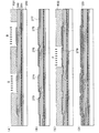
図24に、波長532nmの光に対する非晶質珪素膜の反射率、透過率および吸収率の膜厚依存性を示す。図24のグラフの横軸は非晶質珪素膜の厚さであり、縦軸は反射率、透過率および吸収率の割合を示す。図24から明らかなように、非晶質珪素膜の厚さが50nm以下になると、膜厚の減少に伴って、吸収率が低下し、非晶質珪素膜で反射される、または透過される光量のほうが多くなる。厚さが20nmのときの吸収率は厚さが50nmのときの1/3程度であり、透過率は2倍以上である。 FIG. 24 shows the film thickness dependence of the reflectance, transmittance, and absorptance of the amorphous silicon film with respect to light having a wavelength of 532 nm. In the graph of FIG. 24, the horizontal axis represents the thickness of the amorphous silicon film, and the vertical axis represents the ratio of reflectance, transmittance, and absorptance. As can be seen from FIG. 24, when the thickness of the amorphous silicon film is 50 nm or less, the absorptance decreases as the film thickness decreases, and is reflected or transmitted by the amorphous silicon film. More light. The absorptance when the thickness is 20 nm is about 1 / that when the thickness is 50 nm, and the transmittance is twice or more.
従って、50nmの厚さの非晶質珪素膜を結晶化するときと同様に、20nmの厚さの非晶質珪素膜から大粒径結晶を形成しようすると、レーザビームのエネルギーを非常に高くする必要がある。そのため、高出力でレーザを発振させることとなり、レーザの媒質の寿命が短くなる。また、高いエネルギーを非晶質珪素膜に与えることになるため、レーザビームのエネルギーを最適化することが非常に難しくなり、アブレーションが発生しやすくなる。 Therefore, as in the case of crystallizing an amorphous silicon film having a thickness of 50 nm, if a large grain crystal is formed from an amorphous silicon film having a thickness of 20 nm, the energy of the laser beam is made extremely high. There is a need. Therefore, the laser is oscillated at a high output, and the life of the laser medium is shortened. Further, since high energy is applied to the amorphous silicon film, it is very difficult to optimize the energy of the laser beam, and ablation is likely to occur.
本発明は、上記の問題点に鑑み、レーザビームを照射して、厚さが50nm以下と極薄い半導体膜に大粒径結晶を形成する半導体装置の作製方法を提供するものである。 In view of the above problems, the present invention provides a method for manufacturing a semiconductor device in which a laser beam is irradiated to form a large grain crystal in an extremely thin semiconductor film having a thickness of 50 nm or less.
半導体の代表例である珪素は、その屈折率が約4と非常に大きい。本発明は、このように屈折率の大きい半導体膜に、レーザビームのエネルギーを効率良く熱エネルギーとして吸収させるためのものである。 Silicon, which is a typical example of a semiconductor, has a very high refractive index of about 4. The present invention is for efficiently absorbing the energy of a laser beam as thermal energy in such a semiconductor film having a large refractive index.
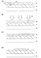
本発明の1つは、半導体膜中でのレーザビームの光路を長くするというものである。そのために、半導体膜の表面に断面が三角形状の複数の凸部を形成する。または、半導体膜が形成される絶縁膜の表面に断面が三角形状の複数の凸部を形成する。本発明では、三角形に、角が多少欠けた三角形や、角が丸みを帯びている三角形も含む。なお、凸部の断面とは、特段の断りがない場合は、半導体膜が形成される基板表面に垂直な面を切断面としたときの断面をいう。 One aspect of the present invention is to lengthen the optical path of a laser beam in a semiconductor film. For this purpose, a plurality of convex portions having a triangular cross section are formed on the surface of the semiconductor film. Alternatively, a plurality of convex portions having a triangular cross section are formed on the surface of the insulating film over which the semiconductor film is formed. In the present invention, the triangle includes a triangle with some missing corners and a triangle with rounded corners. Note that the cross section of the convex portion refers to a cross section when a plane perpendicular to the substrate surface on which the semiconductor film is formed is a cut surface unless otherwise specified.
断面の形状を三角形するには、凸部を錐体状とする、または三角柱とすればよい。本発明では、錐体に、角が多少欠けた錐体や、角が丸みを帯びている錐体も含む。三角柱の場合は、三角柱の底面が凸部の断面になるように、三角柱の側面の1つが基板の表面と平行になるように凸部を形成する。 In order to make the shape of the cross section triangular, the convex portion may be a cone or a triangular prism. In the present invention, the cone includes a cone with some missing corners and a cone with rounded corners. In the case of a triangular prism, the convex portion is formed so that one of the side surfaces of the triangular prism is parallel to the surface of the substrate so that the bottom surface of the triangular prism is a cross section of the convex portion.
半導体膜の屈折率は、半導体膜が接している媒質(例えば、空気や絶縁表面など)の屈折率よりも大きいので、表面に凸部を有する半導体膜に入射したレーザビームは、空気と凸部の界面で反射されながら、半導体膜中をジグザグに進む。すなわち、半導体膜中でのレーザビームの光路が半導体膜の厚さよりも長くなる。これは、半導体膜を厚くしたことと同じこととなり、半導体膜のレーザビームの吸収率を高めることができる。 Since the refractive index of the semiconductor film is larger than the refractive index of a medium (for example, air or an insulating surface) with which the semiconductor film is in contact, the laser beam incident on the semiconductor film having a convex portion on the surface is While being reflected at the interface, the semiconductor film proceeds zigzag. That is, the optical path of the laser beam in the semiconductor film becomes longer than the thickness of the semiconductor film. This is the same as increasing the thickness of the semiconductor film, and the absorption rate of the laser beam of the semiconductor film can be increased.
凸部に入射したレーザビームが凸部と空気との界面で全反射を繰り返すようにするため、半導体膜表面に形成される凸部の断面の三角形は、凸部の先端に対応する頂角が80°以下であることが好ましい。 In order for the laser beam incident on the convex part to repeat total reflection at the interface between the convex part and air, the triangle of the convex section formed on the semiconductor film surface has an apex angle corresponding to the tip of the convex part. It is preferable that it is 80 degrees or less.
また、凸部を有する絶縁膜表面上に半導体膜を形成した場合も同様である。半導体膜を透過したレーザビームを半導体膜と絶縁膜の凸部との界面で全反射させることで、半導体膜内部に戻す。半導体膜中では、レーザビームは、空気と半導体膜の界面、絶縁膜と半導体膜との界面で全反射されながらジグザグに半導体膜中を進む。従って、半導体膜中でのレーザビームの光路が長くなるため、半導体膜のレーザビームの吸収率を高めることができる。 The same applies to the case where a semiconductor film is formed over the surface of the insulating film having a convex portion. The laser beam transmitted through the semiconductor film is totally reflected at the interface between the semiconductor film and the convex portion of the insulating film, thereby returning the laser beam to the inside of the semiconductor film. In the semiconductor film, the laser beam travels through the semiconductor film in a zigzag manner while being totally reflected at the interface between air and the semiconductor film and at the interface between the insulating film and the semiconductor film. Accordingly, since the optical path of the laser beam in the semiconductor film becomes long, the absorption rate of the laser beam in the semiconductor film can be increased.
レーザビームを凸部と半導体膜との界面で全反射させるため、絶縁膜表面に形成される凸部の断面の三角形は、凸部の先端に対応する頂角が140°以下であることが好ましい。 In order to totally reflect the laser beam at the interface between the convex portion and the semiconductor film, it is preferable that the triangle of the cross section of the convex portion formed on the insulating film surface has an apex angle corresponding to the tip of the convex portion of 140 ° or less. .
また、本発明は、半導体膜よりも効率良く、レーザビームを熱として吸収する光吸収膜を半導体膜上に形成し、光吸収膜で吸収した熱を半導体膜に供給することを特徴とする。そのため、光吸収膜は熱伝導率が高く、かつレーザビームに対する透過率が低い膜が選ばれる。光吸収膜の材料には、金属、合金、および金属化合物を用いることができる。金属、合金および金属化合物を構成する金属元素として、モリブデン(Mo)、クロム(Cr)、タングステン(W)、アルミニウム(Al)、タンタル(Ta)、チタン(Ti)、ニッケル(Ni)、白金(Pt)、銅(Cu)、金(Au)、銀(Ag)などの金属元素が選択される。 Further, the present invention is characterized in that a light absorption film that absorbs a laser beam as heat is formed on the semiconductor film more efficiently than the semiconductor film, and heat absorbed by the light absorption film is supplied to the semiconductor film. Therefore, a film having a high thermal conductivity and a low transmittance for the laser beam is selected as the light absorption film. A metal, an alloy, and a metal compound can be used for the material of the light absorption film. As metal elements constituting metals, alloys and metal compounds, molybdenum (Mo), chromium (Cr), tungsten (W), aluminum (Al), tantalum (Ta), titanium (Ti), nickel (Ni), platinum ( Metal elements such as Pt), copper (Cu), gold (Au), and silver (Ag) are selected.
光吸収膜でレーザビームを効率良く吸収させるため、光吸収膜の厚さは600nm以下100nm以上とする。好ましくは、レーザビームの波長と同程度かそれ以下でレーザビームの波長の1/3以上とする。また、光吸収膜の凸部の断面の三角形の底辺の長さは600nm以下100nm以上とする。好ましくは、レーザビームの波長と同程度か、それ以下とし、レーザビームの波長の1/3以上とする。 In order to efficiently absorb the laser beam with the light absorption film, the thickness of the light absorption film is set to 600 nm or less and 100 nm or more. Preferably, it is approximately equal to or less than the wavelength of the laser beam and is not less than 1/3 of the wavelength of the laser beam. Further, the length of the base of the triangle in the cross section of the convex portion of the light absorbing film is 600 nm or less and 100 nm or more. Preferably, it is approximately the same as or shorter than the wavelength of the laser beam, and is 1/3 or more of the wavelength of the laser beam.
また、本発明は、半導体膜表面に反射防止膜を形成し、半導体膜の表面で反射されるレーザビームを少なくすることで、半導体膜でのレーザビームの吸収率を高めることを特徴とする。反射防止膜は、表面に断面が三角形状の凸部を複数有する透光性の膜でなる。よって、反射防止膜には、レーザビームに対する透過率が高く、レーザビームの照射で溶融しない材料でなる膜が選ばれる。例えば、酸化珪素、窒化珪素、酸化窒化珪素を用いることができる。 Further, the present invention is characterized in that the absorption rate of the laser beam in the semiconductor film is increased by forming an antireflection film on the surface of the semiconductor film and reducing the number of laser beams reflected on the surface of the semiconductor film. The antireflection film is a translucent film having a plurality of convex portions having a triangular cross section on the surface. Therefore, a film made of a material that has a high transmittance to the laser beam and does not melt when irradiated with the laser beam is selected as the antireflection film. For example, silicon oxide, silicon nitride, or silicon oxynitride can be used.
反射防止膜でレーザビームの反射を防止する効果を顕在化させるため、反射防止膜の厚さは600nm以下100nm以上とする。好ましくは、レーザビームの波長と同程度かそれ以下とし、レーザビームの波長の1/3以上とする。また、反射防止膜の凸部の断面の三角形の底辺の長さは600nm以下100nm以上とする。好ましくは、レーザビームの波長と同程度かそれ以下、レーザビームの波長の1/3以上とする。 In order to realize the effect of preventing the reflection of the laser beam by the antireflection film, the thickness of the antireflection film is set to 600 nm or less and 100 nm or more. Preferably, it is the same as or shorter than the wavelength of the laser beam, and is 1/3 or more of the wavelength of the laser beam. The length of the base of the triangle in the cross section of the convex portion of the antireflection film is 600 nm or less and 100 nm or more. Preferably, it is approximately equal to or less than the wavelength of the laser beam, and 1/3 or more of the wavelength of the laser beam.
本発明において、半導体膜などの膜の表面に微細な凸部を形成するには、nmレベルの立体構造物を転写技術で形成できるナノインプリント技術を用いればよい。ナノインプリント技術により、レジストマスクを形成し、このレジストマスクを用いて膜をエッチングし、膜表面に凸部を形成する。 In the present invention, in order to form fine convex portions on the surface of a film such as a semiconductor film, a nanoimprint technique that can form a three-dimensional structure at the nm level by a transfer technique may be used. A resist mask is formed by nanoimprint technology, and the film is etched using the resist mask to form convex portions on the film surface.
なお、半導体膜が完全溶融している状態とは、半導体膜が上面から絶縁表面との界面まで溶融している状態、液体になっている状態をいう。上述したように、大粒径結晶を形成するには、レーザビームの照射により半導体膜を完全に溶融させ、固液界面を移動させる必要がある。そのため、レーザには、連続発振レーザまたは疑似連続発振レーザを用いるとよい。パルス発振レーザでも発振周波数が10MHz以上であれば、連続発振レーザと同様の処理ができる。 Note that the state in which the semiconductor film is completely melted refers to a state in which the semiconductor film is melted from the upper surface to the interface with the insulating surface, or a liquid state. As described above, to form a large grain crystal, it is necessary to completely melt the semiconductor film by laser beam irradiation and move the solid-liquid interface. Therefore, a continuous wave laser or a pseudo continuous wave laser is preferably used as the laser. Even with a pulsed laser, if the oscillation frequency is 10 MHz or more, the same processing as that of a continuous wave laser can be performed.
レーザビームの波長は、レーザビームの表皮深さ(skin depth)と結晶化する半導体膜の膜厚を考慮して決定する。半導体膜を完全溶融させ、大粒径結晶を得るためには、レーザビームの波長が400nm〜565nmの範囲で、連続発振レーザまたは疑似連続発振レーザを用いるのが好ましい。例えば、この波長域のレーザビームには、YVO4レーザの第2高調波(532nm)、YAGレーザの第2高調波(532nm)、YLFレーザの第2高調波(527nm)がある。なお、例示したYVO4レーザなどは連続発振レーザにも、パルス発振レーザにも、疑似連続発振レーザにもなる。 The wavelength of the laser beam is determined in consideration of the skin depth of the laser beam and the thickness of the semiconductor film to be crystallized. In order to completely melt the semiconductor film and obtain a large grain crystal, it is preferable to use a continuous wave laser or a pseudo continuous wave laser with a laser beam wavelength in the range of 400 nm to 565 nm. For example, the laser beam in this wavelength region includes the second harmonic (532 nm) of the YVO 4 laser, the second harmonic (532 nm) of the YAG laser, and the second harmonic (527 nm) of the YLF laser. The exemplified YVO 4 laser can be a continuous wave laser, a pulsed laser, or a pseudo continuous wave laser.
レーザビームを照射する前の半導体膜の結晶構造は、非単結晶であればよい。例えば、非晶質、微結晶、多結晶構造である。半導体膜は、代表的には、珪素を主成分とする半導体膜、またはゲルマニウムを主成分とする膜であり、例えば、珪素膜、珪素とゲルマニウムの化合物膜である。半導体膜はCVD法やスパッタ法で形成される。また、半導体膜は、P(リン)、As(ヒ素)のようなn型の不純物、B(ボロン)のようなp型の不純物を含んでいてもよい。 The crystal structure of the semiconductor film before the laser beam irradiation may be a non-single crystal. For example, amorphous, microcrystalline, and polycrystalline structures. The semiconductor film is typically a semiconductor film containing silicon as a main component or a film containing germanium as a main component, for example, a silicon film or a compound film of silicon and germanium. The semiconductor film is formed by a CVD method or a sputtering method. Further, the semiconductor film may contain an n-type impurity such as P (phosphorus) and As (arsenic) and a p-type impurity such as B (boron).
半導体膜が形成される基板は、例えば、ガラス基板、石英基板、サファイヤ基板、およびプラスチック基板などの絶縁材料でなる基板、ステンレス基板などの導電性基板、ならびに半導体基板などである。ステンレス基板などの導電性基板、および半導体基板を用いる場合は、その上面を覆う絶縁膜を形成し、半導体膜が絶縁表面上に形成されるようにするのが好ましい。また、ガラス基板やプラスチック基板など、半導体膜を汚染するような物質を含む基板を用いる場合も、絶縁膜で上面を覆い、半導体膜が汚染されないようにするのが好ましい。また、絶縁膜を厚く形成することで、基板に熱を伝わりにくくする効果がある。基板の上面に形成される絶縁膜には、酸化珪素、窒化珪素、酸化窒化珪素などの単層膜または積層膜を用いることができる。これらの絶縁膜は、CVD法およびスパッタ法で形成することができる。 Examples of the substrate on which the semiconductor film is formed include a glass substrate, a quartz substrate, a sapphire substrate, a substrate made of an insulating material such as a plastic substrate, a conductive substrate such as a stainless steel substrate, and a semiconductor substrate. In the case of using a conductive substrate such as a stainless steel substrate and a semiconductor substrate, it is preferable to form an insulating film covering the upper surface of the semiconductor substrate so that the semiconductor film is formed on the insulating surface. In the case of using a substrate containing a substance that contaminates the semiconductor film, such as a glass substrate or a plastic substrate, it is preferable to cover the upper surface with an insulating film so that the semiconductor film is not contaminated. Further, forming the insulating film thickly has an effect of making it difficult to transfer heat to the substrate. As the insulating film formed over the top surface of the substrate, a single layer film or a stacked film of silicon oxide, silicon nitride, silicon oxynitride, or the like can be used. These insulating films can be formed by a CVD method and a sputtering method.
本発明により、レーザビームのエネルギーを効率良く半導体膜に吸収させることができるため、50nm以下の薄い半導体膜を完全溶融させて結晶化させることが可能になる。よって、大粒径結晶でなる50nm以下の薄い結晶性半導体膜を形成することが可能になる。また、完全溶融に必要なレーザビームのエネルギーを抑えることができるため、レーザへの負担が少なく、レーザビームのエネルギーの最適化が容易になる。 According to the present invention, since the energy of the laser beam can be efficiently absorbed by the semiconductor film, a thin semiconductor film of 50 nm or less can be completely melted and crystallized. Therefore, it is possible to form a thin crystalline semiconductor film having a large grain size and having a thickness of 50 nm or less. In addition, since the energy of the laser beam necessary for complete melting can be suppressed, the burden on the laser is small, and optimization of the energy of the laser beam is facilitated.
本発明の結晶化方法で得られた大粒径結晶でチャネル形成領域を形成することで、高電界効果移動度の薄膜トランジスタを作製することができる。また、チャネル形成領域を50nm以下と薄くすることができるため、薄膜トランジスタを低消費電力化することができる。このような薄膜トランジスタで集積回路を構成することで、低消費電力で、高性能、多機能の半導体装置を製造することができる。 By forming a channel formation region using a large grain crystal obtained by the crystallization method of the present invention, a thin film transistor with high field effect mobility can be manufactured. In addition, since the channel formation region can be as thin as 50 nm or less, the power consumption of the thin film transistor can be reduced. By forming an integrated circuit using such a thin film transistor, a high-performance and multifunctional semiconductor device with low power consumption can be manufactured.
以下に、図面を用いて、本発明の半導体膜の結晶化方法を説明する。ただし、本発明は多くの異なる態様で実施することが可能であり、本発明の趣旨およびその範囲から逸脱することなくその形態および詳細を様々に変更し得ることは当業者であれば容易に理解される。従って、本発明は本実施の形態の記載内容に限定して解釈されるものではない。 The method for crystallizing a semiconductor film of the present invention will be described below with reference to the drawings. However, those skilled in the art can easily understand that the present invention can be implemented in many different modes, and that the modes and details can be variously changed without departing from the spirit and scope of the present invention. Is done. Therefore, the present invention should not be construed as being limited to the description of the embodiment modes.
(実施の形態1)
本実施の形態では、断面が三角形の凸部を半導体膜の表面に形成して、半導体膜を結晶化する方法を説明する。図1乃至図5を用いて、半導体膜の結晶化方法を説明する。
(Embodiment 1)
In this embodiment, a method for crystallizing a semiconductor film by forming a convex portion having a triangular cross section on the surface of the semiconductor film will be described. A method for crystallizing a semiconductor film will be described with reference to FIGS.
図1(A)に示すように、基板10上に、下地となる絶縁膜11を形成する。絶縁膜11として、プラズマCVD法、スパッタ法により、酸化珪素膜、窒化珪素膜、窒化酸化珪素膜、酸化窒化珪素膜の単層膜または多層膜を形成する。絶縁膜11の厚さは50nm〜200nmとする。絶縁膜11上に半導体膜12を形成する。例えば、珪素膜を形成する場合は、水素で希釈したシラン(SiH4)またはジシラン(Si2H6)を原料ガスに用いて、プラズマCVD法、減圧CVD法または熱CVD法などで形成する。珪素膜にゲルマニウムを添加するには、原料ガスにGeH4を添加すればよい。また、スパッタ法で珪素膜を形成する場合は、珪素(Si)のターゲットを用いればよく、ゲルマニウムを添加するには、ターゲットにGeを添加すればよい。
As shown in FIG. 1A, an insulating
次に、半導体膜12の表面に断面が三角形の凸部12aを形成する。例えば、ナノインプリント法により、フォトレジストでマスクを形成し、このマスクを用いて半導体膜12をドライエッチングする。なお、半導体膜12の表面の凸部12aは、図2に示すような三角柱状または、図3に示すような錐体であればよい。凸部12aの断面が三角形であればよいので、錐体は角錐、円錐いずれでもよい。図3では正六角錐の例を示している。
Next, a
半導体膜12の表面に、基板と平行な平面が無いように、または少なくなるように、凸部12aを形成することが好ましい。これは、凸部12aからレーザビームLBを半導体膜12の内部に入射させることが、半導体膜12の吸収率の向上に寄与するからである。図2および図3は、半導体膜12の表面に基板と平行な平面が無いように、凸部12aを形成した例である。凸部12aを錐体とする場合は、平面を錐体で充填できるような三角錐、四角錐、および六角錐などが好ましい。
The
半導体膜12の表面に凸部12aを形成した後、図1(B)に示すように、半導体膜12の上方からレーザビームLBを照射する。発振器から射出されたレーザビームLBは点状であるため、シリンドリカルレンズなどを含む光学系により、被照面で線状になるように整形される。線状のレーザビームLBをその短尺方向に平行な方向に走査しながら照射する。原料ガスにシランなどを用いた場合など、成膜方法によって、半導体膜12が水素を含むことがある。レーザビームLBを照射したとき、半導体膜12から水素が噴出しないようにするため、400℃〜550℃で1時間程度かそれ以上加熱し、半導体膜12の水素出しを行う。
After the
図4を用いて、半導体膜12の凸部12aの作用を説明する。珪素の屈折率は約4と極めて大きい。そのため、半導体膜12の凸部12aに入射したレーザビームLBは大きく屈折され、凸部12aと空気との界面で全反射されながら、基板10に向かって進む。つまり、レーザビームLBが半導体膜12の凸部12a内をジグザグに進むため、その光路が半導体膜12の膜厚よりも長くなる。半導体膜12中の光路長が長くなることは、半導体膜12を厚くしたことと同様であるため、半導体膜12の吸収率が増加する。
The operation of the
また、凸部12aからレーザビームLBを半導体膜12内に入射させているため、絶縁膜11と半導体膜12の界面に入射したレーザビームLBが全反射する確率が高くなり、また全反射されたレーザビームLBは半導体膜12と空気との界面でも全反射される。従って、レーザビームLBが半導体膜12中を伝搬している時間が長くなり、熱として半導体膜に吸収される光量が増加する。
In addition, since the laser beam LB is incident on the
凸部12aの効果は、凸部12aでレーザビーム全反射させること、絶縁膜11と半導体膜12の界面および空気と半導体膜12の界面でレーザビームを全反射させて、半導体膜12内にレーザビームを閉じこめること、以上の2点にある。これらの効果により、半導体膜12の吸収率を向上させることができる。
The effect of the
屈折率が、それぞれ、空気は約1、半導体膜12は3〜5程度、絶縁膜11は1.4〜1.6程度であるため、凸部12aを形成する効果を顕在化するには、凸部12aの断面の三角形の頂角α1を80°以下とする。また、凸部12aの高さd1(半導体膜12の厚さが変化している部分の厚さd1)のほうが、半導体膜12の厚さが変化しない部分の厚さd2よりも厚く、好ましくは2倍以上とする。また、厚さd2を殆ど0にして、半導体膜12は凸部12aのみになるように形成してもよい。
The refractive index is about 1 for air, about 3 to 5 for the
凸部12aの効果により、半導体膜12でのレーザビームLBの吸収率を向上させることができるため、レーザビームLBの照射により半導体膜12を完全溶融させて、厚さが50nm以下の大粒径結晶でなる結晶性半導体膜13を形成することができる。半導体膜12を完全溶融させることで、図1(C)に示すように、溶融後の結晶性半導体膜13の表面は平坦化される。なお、光は高速なため、凸部12aでレーザビームLBが全反射されている間は、凸部12aが溶融することなくその形状を維持することができるので、凸部12aの機能を発揮させることができる。
The absorption ratio of the laser beam LB in the
結晶化する前の半導体膜12の厚さは、結晶化後の結晶性半導体膜13の厚さDを考慮して決定することができる。図2のように凸部12aを三角柱状にした場合は、D=d1/2+d2の式を考慮し、図3のように凸部12aを錐体にした場合は、D=d1/3+d2の式を考慮し、さらに、結晶化前の半導体膜12と結晶化後の結晶性半導体膜14の密度を考慮すればよい。上記の2つの式から分かるように、凸部12aを設けることで、結晶化前の半導体膜12全体を厚くする効果も生ずる。特に、d2を小さくするほど、半導体膜12全体の厚さを大きくすることができる。
The thickness of the
図1(D)に示すように、結晶性半導体膜14を、フォトリソグラフィおよびエッチングにより島状に加工し、島状の結晶性半導体膜14を形成する。この結晶性半導体膜14を用いて、トランジスタ、ダイオード、コンデンサ、不揮発性メモリ素子などの半導体素子を形成する。これらの半導体素子を組み合わせて集積回路など、各種の半導体装置を形成する。
As shown in FIG. 1D, the
例えば、図5に示すように、島状の結晶性半導体膜14を用いて薄膜トランジスタを形成する。結晶性半導体膜14にゲート絶縁膜17が形成され、ゲート絶縁膜17上にゲート電極18が形成される。n型またはp型の不純物を島状結晶性半導体膜14に添加し、高濃度不純物領域14bを形成する。その結果、島状結晶性半導体膜14にチャネル形成領域14aが確定される。ゲート電極18上に層間絶縁膜19を形成する。層間絶縁膜19およびゲート絶縁膜17に、島状結晶性半導体膜14に達するコンタクトホールを形成する。層間絶縁膜19上に電極20を形成し、電極20を高濃度不純物領域14bに接続する。以上の工程により、薄膜トランジスタが製造される。
For example, as illustrated in FIG. 5, a thin film transistor is formed using an island-shaped
大粒径結晶でチャネル形成領域14aを形成することで、電界効果移動度が高い薄膜トランジスタを作製することができる。また、チャネル形成領域14aを50nm以下と薄くすることができるため、サブスレッショルド値(S値)が改善され、しきい値電圧の絶対値を小さくすることができるため、駆動電圧を抑えることができる。このような薄膜トランジスタを用いることで、低消費電力で、高性能、多機能の半導体装置を製造することができる。
By forming the
(実施の形態2)
本実施の形態では、表面に断面が三角形の凸部を有する絶縁膜上に半導体膜を形成して、半導体膜を結晶化する方法を説明する。図6乃至図7を用いて、半導体膜の結晶化方法を説明する。
(Embodiment 2)
In this embodiment mode, a method for crystallizing a semiconductor film by forming a semiconductor film over an insulating film having a convex portion with a triangular cross section on the surface will be described. A semiconductor film crystallization method will be described with reference to FIGS.
図6(A)に示すように、基板10上に、下地となる絶縁膜41を形成する。絶縁膜41として、プラズマCVD法、スパッタ法により、酸化珪素膜、窒化珪素膜、酸化窒化珪素膜の単層膜または多層膜を形成する。絶縁膜41の厚さは10nm〜200nmとする。
As shown in FIG. 6A, an insulating
次に、図6(B)に示すように、絶縁膜41の表面に断面が三角形の凸部41aを形成する。例えば、ナノインプリント法により、フォトレジストでマスクを形成し、このマスクを用いて絶縁膜41をドライエッチングする。なお、絶縁膜41の表面の凸部41aの形状は、図1(A)の半導体膜12の凸部12aと同じように、三角柱状または錐体とする(図2および図3参照)。また、配置も凸部12aと同様であり、絶縁膜41の表面に基板10の表面と平行な面が無いように、または少なくなるように、凸部41aを形成する。
Next, as shown in FIG. 6B, a
図6(A)に示すように、絶縁膜41に接して、半導体膜42を形成する。半導体膜42は、プラズマCVD法、減圧CVD法、熱CVD法またはスパッタ法で、珪素膜、ゲルマニウム膜、ゲルマニウムを含む珪素膜を形成する。図6の例では、半導体膜42の下地が平坦でないため、半導体膜42を成膜した後、CMP法などの研磨法を用いて、半導体膜42の表面を平坦化するのが好ましい。平坦化された後の半導体膜42において、凸部41aを含まない部分の厚さd3が50nm以下10nm以上となるようにする。また、凸部41aの厚さd4は、50nm以下10nm以上が好ましい。
As shown in FIG. 6A, a
図6(B)に示すように、半導体膜42の上方から線状レーザビームLBを照射する。必要に応じて、レーザビームLBを照射する前に、400℃〜550℃で、1時間程度かそれ以上の加熱処理により、半導体膜42の水素出しを行う。
As shown in FIG. 6B, the linear laser beam LB is irradiated from above the
図7を用いて、絶縁膜41の凸部41aの作用を説明する。シリコンの屈折率は約4であり、ゲルマニウムの屈折率は約3と極めて大きいため、半導体膜42に入射したビームは、基板10の表面にほぼ垂直な方向から、絶縁膜41に向かって進む。絶縁膜41の凸部41aとの界面に達したレーザビームLBは、この界面で全反射される。凸部41aと半導体膜42との界面で全反射されることで、半導体膜42の上面へ進むように光路が偏向される。レーザビームLBは、空気と半導体膜12の上面との界面でも全反射され、再び、絶縁膜41の方向に偏向される。
The operation of the
図7に示すように、全反射しながらレーザビームLBは半導体膜42内をジグザグに進むため、レーザビームLBが半導体膜42中を伝搬する時間が長くなるので、半導体膜42の吸収率を向上させることができる。すなわち、本実施の形態では、従来、半導体膜42を透過していたレーザビームLBを凸部41aで全反射させることで半導体膜42中に閉じこめることで、熱として半導体膜42に吸収させている。
As shown in FIG. 7, the laser beam LB proceeds in a zigzag manner in the
屈折率が、半導体膜42は3〜5程度、絶縁膜41は1.4〜1.6程度であるため、凸部41aと半導体膜42との界面で全反射をさせる効果を顕在化させるため、凸部41aの断面の三角形の頂角α2は140°以下が好ましい。
Since the refractive index is about 3 to 5 for the
凸部41aの効果により、レーザビームLBを半導体膜42に吸収させて、半導体膜42を完全溶融させることができるため、レーザビームLBの照射により大粒径結晶でなる結晶性半導体膜43を形成することができる(図6(C)参照。)。
Due to the effect of the
図6(D)に示すように、結晶性半導体膜43を、フォトリソグラフィおよびエッチングにより島状に加工し、島状の結晶性半導体膜44を形成する。この結晶性半導体膜44を用いて、例えば、図5に示すような薄膜トランジスタを形成することができる。また、トランジスタの他、ダイオード、コンデンサ、不揮発性メモリ素子などの半導体素子を形成することができる。これらの半導体素子を組み合わせて集積回路など、各種の半導体装置が形成される。
As shown in FIG. 6D, the
(実施の形態3)
本実施の形態では、断面が三角形の凸部を有する光吸収膜を半導体膜の表面に形成して、半導体膜を結晶化する方法を説明する。図8および図9を用いて、半導体膜の結晶化方法を説明する。
(Embodiment 3)
In this embodiment mode, a method for crystallizing a semiconductor film by forming a light absorption film having a convex portion with a triangular cross section on the surface of the semiconductor film will be described. A semiconductor film crystallization method will be described with reference to FIGS.
図8(A)に示すように、基板50上に、実施の形態1と同様に、下地となる絶縁膜51を形成し、絶縁膜51上に半導体膜52を形成する。なお、本実施の形態では、半導体膜52の表面に凸部を形成しない。半導体膜52の厚さは10nm以上50nm以下とする。
As shown in FIG. 8A, an insulating
次に、半導体膜52上に、光吸収膜54を形成する。光吸収膜54は、レーザビームを熱として吸収し、かつ吸収した熱を半導体膜に伝えるための膜である。そのため、光吸収膜54は熱伝導率が高く、かつレーザビームに対する透過率が低い膜が選ばれる。光吸収膜54の材料には、金属、合金、および金属化合物を用いることができる。金属、合金および金属化合物を構成する金属元素として、モリブデン(Mo)、クロム(Cr)、タングステン(W)、アルミニウム(Al)、タンタル(Ta)、チタン(Ti)、ニッケル(Ni)、白金(Pt)、銅(Cu)、金(Au)、銀(Ag)などの金属元素が選択される。
Next, a
このような材料でなる膜を半導体膜52に接するように形成することは好ましくない。そのため、半導体膜52の表面に保護絶縁膜53を10nm〜100nmの厚さで形成する。保護絶縁膜53として、プラズマCVD法、スパッタ法により、酸化珪素膜、窒化珪素膜、酸化窒化珪素膜の単層膜または多層膜を形成する。
It is not preferable to form a film made of such a material so as to be in contact with the
保護絶縁膜53を形成した後、光吸収膜54を構成する膜を形成する。本実施の形態では、モリブデン膜をスパッタ法で成膜する。モリブデン膜の表面に断面が三角形の凸部54aを形成し、光吸収膜54を形成する。凸部54aは、ナノインプリント法により、フォトレジストでマスクを形成し、このマスクを用いてモリブデン膜の表面をドライエッチングする。なお、光吸収膜54の表面の凸部54aの形状は、図1(A)の半導体膜12の凸部12aと同じであり、三角柱状または錐体とする(図2および図3参照)。また、配置も凸部12aと同様であり、光吸収膜54の表面に基板50の表面と平行な面が無いように、または少なくなるように凸部54aを形成する。
After forming the protective insulating
光吸収膜54の表面に凸部54aを形成した後、図8(B)に示すように、半導体膜52の上方からレーザビームLBを照射する。必要に応じて、レーザビームLBを照射する前に、半導体膜52および保護絶縁膜53の水素出しを行う。
After the
照射されたレーザビームLBは光吸収膜54で殆どが吸収され、光吸収膜54が加熱される。光吸収膜54が加熱されることで、半導体膜52も温度上昇し、完全溶融することで、図8(C)に示すように、大粒径結晶を有する結晶性半導体膜56を形成することができる。このように、光吸収膜54によりレーザビームLBのエネルギーを熱として、半導体膜52に効率良く供給することができるため、レーザの出力を抑えることができる。
The irradiated laser beam LB is mostly absorbed by the
光吸収膜54の表面でレーザビームLBの反射を抑えるため、光吸収膜54の厚さd5(凸部54aの高さd5)および、凸部54aの断面の三角形の底辺の長さd6は、それぞれ、レーザビームLBの波長λと同程度か、それ以下とし、600nm以下100nm以上とすればよい。より好ましくは、1/3λ≦d5≦λ、1/3λ≦d6≦λとする。
In order to suppress the reflection of the laser beam LB on the surface of the
レーザビームLBを照射した後、光吸収膜54をエッチングにより除去する。保護絶縁膜53をゲート絶縁膜などの半導体素子を構成する膜として用いる場合は、図9(A)に示すように、保護絶縁膜53ともに、結晶性半導体膜56をフォトリソグラフィおよびエッチングにより島状に加工し、島状の結晶性半導体膜57および島状の絶縁膜58を形成する。半導体素子を構成する膜として保護絶縁膜53を用いない場合は、保護絶縁膜53を除去し、図9(B)に示すように、結晶性半導体膜56をフォトリソグラフィおよびエッチングにより島状に加工し、島状の結晶性半導体膜57を形成する。
After the irradiation with the laser beam LB, the
図9(A)および図9(B)に示す結晶性半導体膜57を用いて、例えば、図5に示すような薄膜トランジスタを形成することができる。図9(A)の島状の絶縁膜58は薄膜トランジスタのゲート絶縁膜17を構成することとなる。トランジスタの他、ダイオード、コンデンサ、不揮発性メモリ素子などの半導体素子を形成することができる。これらの半導体素子を組み合わせて集積回路など、各種の半導体装置が形成される。
A thin film transistor as shown in FIG. 5 can be formed using the
(実施の形態4)
本実施の形態では、断面が三角形の凸部を有する反射防止膜を半導体膜の表面に形成して、半導体膜を結晶化する方法を説明する。図10を用いて、半導体膜の結晶化方法を説明する。
(Embodiment 4)
In this embodiment mode, a method for crystallizing a semiconductor film by forming an antireflection film having a convex portion with a triangular cross section on the surface of the semiconductor film will be described. A method for crystallizing a semiconductor film will be described with reference to FIG.
図10(A)に示すように、基板70上に、実施の形態1と同様に、下地となる絶縁膜71を形成し、絶縁膜71上に半導体膜72を形成する。なお、本実施の形態では、半導体膜72の表面に凸部を形成しない。半導体膜72の厚さは10nm以上50nm以下とする。
As shown in FIG. 10A, an insulating
次に、反射防止膜74を構成する透光性の膜を形成する。反射防止膜74を通過させてレーザビームLBを半導体膜72に照射するため、反射防止膜74の材料には、レーザビームLBに対する透過率が高く、またレーザビームLBの照射で溶融しない材料が選ばれる。例えば、反射防止膜74には酸化珪素膜、窒化珪素膜、酸化窒化珪素膜など絶縁膜の単層膜または多層膜を用いることができる。これらの膜はプラズマCVD法、スパッタ法により形成される。
Next, a translucent film constituting the
本実施の形態では、CVD法で酸化珪素膜を成膜する。酸化珪素膜の表面に断面が三角形の凸部74aを形成し、反射防止膜74とする。凸部74aは、ナノインプリント法により、フォトレジストでマスクを形成し、このマスクを用いてモリブデン膜の表面をドライエッチングする。なお、反射防止膜74の表面の凸部74aの形状は、図1(A)の半導体膜12の凸部12aと同じであり、三角柱状または錐体とする(図2および図3参照)。また、配置も凸部12aと同様であり、反射防止膜74の表面に基板70の表面と平行な面が無いように、または少なくなるように凸部74aを形成する。
In this embodiment, a silicon oxide film is formed by a CVD method. A
反射防止膜74の表面に凸部74aを形成した後、図10(B)に示すように、半導体膜72の上方からレーザビームLBを照射する。必要に応じて、レーザビームLBを照射する前に、半導体膜72および反射防止膜74の水素出しを行っておく。
After the
上方から照射されたレーザビームLBの殆どは反射防止膜74の凸部74aで反射されることなく、凸部74aで屈折される。すなわち、反射防止膜74を設けていないとき半導体膜72表面で反射していた光を、反射防止膜74を設けることで、半導体膜72に入射させることができる。従って、半導体膜72の反射率が低下し、吸収率が増加することになるため、レーザを高出力にせずに、厚さ50nm以下の半導体膜72を完全溶融させることが可能になる。
Most of the laser beam LB irradiated from above is not reflected by the
凸部74aでのレーザビームLBの反射を抑えるため、反射防止膜74の厚さd7(凸部74aの高さd7)および、凸部74aの断面の三角形の底辺の長さd8は、それぞれ、レーザビームLBの波長λと同程度かそれ以下とし、600nm以下100nm以上の範囲で決めることができる。より好ましくは、1/3λ≦d7≦λ、1/3λ≦d8≦λとする。
In order to suppress the reflection of the laser beam LB at the
レーザビームLBを照射して、図10(C)に示すように結晶性半導体膜76を形成した後、反射防止膜74をエッチングにより除去する。図10(D)に示すように、結晶性半導体膜76をフォトリソグラフィおよびエッチングにより島状に加工し、島状の結晶性半導体膜77を形成する。この結晶性半導体膜77を用いて、例えば、図5に示すような薄膜トランジスタを形成することができる。なお、トランジスタの他、ダイオード、コンデンサ、不揮発性メモリ素子などの半導体素子を形成することができる。これらの半導体素子を組み合わせて集積回路など、各種の半導体装置が形成される。
After irradiation with the laser beam LB to form a
本実施例では、図11、図12を用いて、半導体素子である不揮発性メモリ素子の作製方法の一例を説明する。 In this embodiment, an example of a method for manufacturing a nonvolatile memory element which is a semiconductor element will be described with reference to FIGS.
本実施例で示す不揮発性メモリ素子は、MOSFET(Metal Oxide Semiconductor Field effect transistor)と類似の構造を有し、電荷を長期間蓄積することのできる領域がチャネル形成領域上に設けられている。この電荷蓄積領域は絶縁膜上に形成され、周囲と絶縁分離されていることから浮遊ゲート電極とも呼ばれる。浮遊ゲート電極上には、絶縁膜を介して制御ゲート電極を備えている。 The nonvolatile memory element shown in this embodiment has a structure similar to that of a MOSFET (Metal Oxide Semiconductor Field Effect Transistor), and a region in which charges can be accumulated for a long period is provided on the channel formation region. This charge storage region is formed on an insulating film and is also called a floating gate electrode because it is isolated from the surroundings. A control gate electrode is provided on the floating gate electrode through an insulating film.
上記のような構造を有する不揮発性メモリ素子は、制御ゲート電極に印加する電圧により、浮遊ゲート電極に電荷を蓄積させ、また放出させる動作が行われる。すなわち浮遊ゲート電極に保持させる電荷の出し入れにより、データを記憶する仕組みになっている。浮遊ゲート電極への電荷の注入や引き抜きは、チャネル形成領域が形成される半導体膜と、制御ゲート電極の間に高電圧を印加する。このときチャネル形成領域上の絶縁膜には、ファウラー−ノルドハイム(Fowler−Nordheim)型(F−N型)トンネル電流(NAND型)や、熱電子(NOR型)が流れるといわれている。チャネル形成領域上に設けられる絶縁膜は、トンネル絶縁膜とも呼ばれている。 In the nonvolatile memory element having the above-described structure, an operation for accumulating and releasing charges in the floating gate electrode is performed by a voltage applied to the control gate electrode. In other words, data is stored by taking in and out the electric charge held in the floating gate electrode. In order to inject or withdraw charges from the floating gate electrode, a high voltage is applied between the semiconductor film in which the channel formation region is formed and the control gate electrode. At this time, it is said that Fowler-Nordheim type (FN type) tunnel current (NAND type) and thermal electrons (NOR type) flow through the insulating film on the channel formation region. The insulating film provided over the channel formation region is also called a tunnel insulating film.
まず、図11(A)に示すように、基板500上に下地膜となる絶縁膜501を形成する。絶縁膜501上に、実施の形態1乃至4のいずれかの結晶化方法を用いて、結晶性珪素膜を形成し、フォトリソグラフィ工程およびエッチング工程により島状の結晶性半導体膜510を形成する。なお、本実施例では、実施の形態1、3および4で説明した、下地の絶縁膜501に凸部を形成しない結晶化方法を用いている。実施の形態2の方法と用いる場合は、絶縁膜501に断面が三角形の凸部を形成する。結晶性半導体膜510の厚さは50nm以下、好ましくは50nm以下10nm以上とする。
First, as illustrated in FIG. 11A, an insulating
図11(B)に示すように、結晶性半導体膜510上に第1の絶縁膜511を形成する。第1の絶縁膜511は、CVD法やスパッタ法等を用いて、酸化珪素、酸化窒化珪素等の珪素を主成分とする絶縁材料を用いて形成することができる。また、酸化アルミニウム、酸化タンタル、酸化ハフニウム等の金属酸化物を主成分とする材料を用いて形成することもできる。第1の絶縁膜511は、膜厚1nm以上20nm以下、好ましくは膜厚1nm以上10nm以下で形成する。
As shown in FIG. 11B, a first
次に、図11(C)に示すように、第1の絶縁膜511に対してプラズマ酸化を行い、第2の絶縁膜512を形成する。第2の絶縁膜512上に電荷蓄積膜513を形成する。第2の絶縁膜512はトンネル絶縁膜として機能し、電荷蓄積膜513は浮遊ゲート電極として機能する。
Next, as shown in FIG. 11C, plasma oxidation is performed on the first insulating
第1の絶縁膜511に対して行うプラズマ酸化は、マイクロ波(代表的には2.45GHz)等の高周波で励起され、電子密度が1×1011cm−3以上であり、プラズマの電子温度が1.5eV以下のプラズマを利用する。電子密度が1×1011cm−3以上1×1013cm−3以下で、プラズマの電子温度が0.5eV以上1.5eV以下のプラズマを利用することが好ましい。また、第1の絶縁膜511に対するプラズマ酸化時間は、60秒以上が好ましい。
The plasma oxidation performed on the first insulating
プラズマ酸化の雰囲気は、少なくとも酸素(O2)を含む雰囲気、少なくとも一酸化二窒素(N2O)および希ガスを含む雰囲気、少なくとも酸素、水素(H2)および希ガスを含む雰囲気、または少なくとも一酸化二窒素、水素および希ガスを含む雰囲気である。なお、雰囲気に水素を含む場合は、その割合を酸素、一酸化二窒素および希ガスよりも少なくするのが好ましい。 The atmosphere of plasma oxidation is an atmosphere containing at least oxygen (O 2 ), an atmosphere containing at least dinitrogen monoxide (N 2 O) and a rare gas, an atmosphere containing at least oxygen, hydrogen (H 2 ), and a rare gas, or at least An atmosphere containing dinitrogen monoxide, hydrogen, and a rare gas. Note that in the case where the atmosphere contains hydrogen, the proportion is preferably smaller than oxygen, dinitrogen monoxide, and a rare gas.
希ガスとしては、代表的には、Arガス、またはArとKrの混合ガスが用いられる。プラズマ酸化の雰囲気が希ガスを含む場合、第2の絶縁膜512は、プラズマ処理に用いた希ガスを含む場合がある。例えば、プラズマ酸化にArを用いた場合には、第2の絶縁膜512にArが含まれる場合がある。
As the rare gas, Ar gas or a mixed gas of Ar and Kr is typically used. In the case where the atmosphere of plasma oxidation includes a rare gas, the second
プラズマ酸化は、プラズマの電子密度が1×1011cm−3以上と高密度であり、被処理物である第1の絶縁膜511付近での電子温度が低いため、第2の絶縁膜512がプラズマにより損傷することを防止することができる。また、プラズマの電子密度が1×1011cm−3以上と高密度であるため、被処理物(ここでは第1の絶縁膜511)をプラズマ酸化することによって形成される膜(ここでは第2の絶縁膜512)は、CVD法やスパッタ法等により形成された膜と比較して緻密で高耐圧な膜を形成することができる。また、プラズマの電子温度が1.5eV以下と低いため、従来のプラズマ処理や熱酸化法と比較して低温度で、被処理物の酸化処理を行うことができる。例えば、ガラス基板の歪点よりも100℃以上低い、500℃〜650℃温度でプラズマ酸化を行っても十分に酸化処理を行うことができる。
In the plasma oxidation, since the electron density of plasma is as high as 1 × 10 11 cm −3 or more and the electron temperature in the vicinity of the first insulating
水素が含まれる絶縁膜をプラズマ酸化することで、水素含有量が低減された膜を得ることができる。 By performing plasma oxidation on the insulating film containing hydrogen, a film with a reduced hydrogen content can be obtained.
本実施例では、酸素(O2)とアルゴン(Ar)との混合ガスの雰囲気下で、第1の絶縁膜511をプラズマ酸化する。プラズマ酸化の雰囲気に、例えば、酸素を0.1〜100sccm、アルゴンを100〜5000sccmの範囲で導入すればよい。
In this embodiment, the first insulating
第1の絶縁膜511に対してプラズマ酸化することにより形成された第2の絶縁膜512は、不揮発性メモリ素子のトンネル絶縁膜として機能する。従って、第2の絶縁膜512が薄いほどトンネル電流が流れやすくなる。また、第2の絶縁膜512が薄いほど、後に形成される浮遊ゲート電極に低電圧で電荷を蓄積させることが可能となる。
The second
一般的に、半導体膜上に絶縁膜を薄く形成する方法として熱酸化法があるが、基板500に、ガラス基板のような歪み点が700℃未満の基板を用いる場合には、半導体膜を熱酸化して、トンネル絶縁膜を形成することは非常に困難である。また、CVD法やスパッタ法により形成した絶縁膜は、膜の内部に欠陥を含んでいるため耐圧が十分でない。さらに、CVD法やスパッタ法により膜厚の薄い絶縁膜を形成した場合には絶縁耐圧が低く、かつピンホール等の欠陥が生じやすい問題がある。従って、CVD法やスパッタ法により形成した第1の絶縁膜511をそのままトンネル絶縁膜として用いると、不良が生じやすい。
Generally, there is a thermal oxidation method as a method for forming a thin insulating film on a semiconductor film. However, when a substrate having a strain point of less than 700 ° C. such as a glass substrate is used as the
そこで、本実施例で示すように、第1の絶縁膜511をプラズマ酸化して第2の絶縁膜512を形成することで、CVD法やスパッタ法等により形成した絶縁膜より緻密で高耐圧な膜を形成することができる。また、第1の絶縁膜511形成時に結晶性半導体膜510の端部を十分に被覆できなかった場合でも、プラズマ酸化することで、半導体膜を十分に被覆する第2の絶縁膜512を形成することができる。
Therefore, as shown in this embodiment, the first insulating
本実施例の不揮発性メモリ素子は、トンネル絶縁膜を介して電子を注入することによって情報を記憶する。このとき、トンネル絶縁膜に電子トラップの要因となる水素が存在すると、書き込みおよび消去を繰り返すうちに電圧が変動してしまい、メモリが劣化する原因となる。従って、電子トラップの要因となるトンネル絶縁膜中の水素含有量は少ないほうが好ましい。第1の絶縁膜511をプラズマ酸化して第2の絶縁膜512を形成することで、CVD法やスパッタ法等により形成した絶縁膜より膜中の水素含有量を低減することができる。
The nonvolatile memory element of this embodiment stores information by injecting electrons through the tunnel insulating film. At this time, if hydrogen that causes electron traps exists in the tunnel insulating film, the voltage fluctuates as writing and erasing are repeated, which causes deterioration of the memory. Accordingly, it is preferable that the hydrogen content in the tunnel insulating film, which causes an electron trap, is small. By forming the second
以上のように、チャネル形成領域が形成される結晶性半導体膜510を40nm以下と薄く形成し、また電子密度が高い酸素プラズマ酸化によりトンネル絶縁膜を酸化することにより、低消費電力で、高速動作可能な不揮発性メモリ素子を形成することができる。
As described above, the
電荷蓄積膜513は、単層膜または2層以上の積層膜で形成することができる。例えば、電荷蓄積膜513を構成する層は、珪素(Si)、ゲルマニウム(Ge)などの半導体材料、珪素を主成分とする化合物、タングステン(W)、チタン(Ti)、タンタル(Ta)、モリブデン(Mo)等から選ばれた金属、これら金属を主成分とする合金、およびこれら金属を主成分とする金属化合物(金属窒化物、金属酸化物等)から選ばれた材料を用いて形成することができる。
The
例えば、珪素を主成分とする化合物として、窒化珪素、窒化酸化珪素、炭化珪素、およびシリサイド(タングステンシリサイド、チタンシリサイド、ニッケルシリサイド)などがある。半導体材料として、n型またはp型の珪素、およびゲルマニウムを10原子%未満の濃度で含む珪素ゲルマニウムなどがある。金属の化合物として、窒化タンタル、酸化タンタル、窒化タングステン、窒化チタン、酸化チタンおよび酸化スズなどがある。また、珪素を用いる場合は、リンやボロンなどの導電性を付与する不純物を添加してもよい。 For example, as a compound containing silicon as a main component, there are silicon nitride, silicon nitride oxide, silicon carbide, silicide (tungsten silicide, titanium silicide, nickel silicide), and the like. Examples of the semiconductor material include n-type or p-type silicon and silicon germanium containing germanium at a concentration of less than 10 atomic%. Examples of the metal compound include tantalum nitride, tantalum oxide, tungsten nitride, titanium nitride, titanium oxide, and tin oxide. In the case of using silicon, an impurity imparting conductivity such as phosphorus or boron may be added.
図11(D)に示すように、電荷蓄積膜513上に第3の絶縁膜514を形成する。第3の絶縁膜514の膜厚は1nm以上100nm以下とし、20nm以上60nm以下が望ましい。第3の絶縁膜514は、酸化珪素、酸化窒化珪素等の珪素を主成分とする絶縁材料、または、酸化アルミニウム、酸化タンタル、酸化ハフニウム等の金属酸化物で形成する。これらの膜はCVD法やスパッタ法等を用いて形成する。
As shown in FIG. 11D, a third
第1の絶縁膜511の酸化プラズマ処理と同様に、第3の絶縁膜514に対してプラズマ酸化を行う。図12(A)に示すように、第3の絶縁膜514に対してプラズマ酸化を行うことにより第4の絶縁膜515を形成する。次に、第4の絶縁膜515上に導電膜516、導電膜517を順に積層する。
Plasma oxidation is performed on the third
導電膜516、517は、ゲート電極(コントロールゲート電極)を構成する導電膜である。2層の導電膜でゲート電極を形成する例を示したが、単層でも3層以上でもよい。コントロールゲート電極を構成する導電膜は、n型またはp型の珪素、タンタル(Ta)、タングステン(W)、チタン(Ti)、モリブデン(Mo)、アルミニウム(Al)、銅(Cu)、クロム(Cr)、ニオブ(Nb)等の金属、これらの金属を主成分とする合金、およびこれら金属を主成分とする金属化合物(金属窒化物、金属酸化物等)から選択された材料で形成することができる。
The
フォトリソグラフィ工程によりレジストマスクを形成する。このレジストマスクを用いて導電膜516、914をエッチングし、図12(B)に示すように、結晶性半導体膜510上にゲート電極520を形成する。さらに、ゲート電極520をマスクにして、第4の絶縁膜515および電荷蓄積膜513をエッチングする。その結果、ゲート電極520、第4の絶縁膜515、電荷蓄積膜513の側面が概略一致するように形成される。電荷蓄積膜513は浮遊ゲート電極として機能し、第4の絶縁膜515はコントロール絶縁膜として機能し、ゲート電極520は制御ゲート電極として機能する。
A resist mask is formed by a photolithography process. The
図12(C)に示すように、ゲート電極520をマスクとして、n型またはp型を付与する不純物を添加し、一対の不純物領域522と、一対の不純物領域522間に位置するチャネル形成領域523を形成する。n型を付与する不純物にはリン(P)やヒ素(As)等を用い、p型を示す不純物にはボロン(B)等を用いることができる。n型またはp型を付与する不純物を添加した後、この不純物を活性化する熱処理を行う。
As shown in FIG. 12C, an impurity imparting n-type or p-type is added using the
図12(D)に示すように、ゲート電極520を覆うように第6の絶縁膜524を形成する。第6の絶縁膜524および第2の絶縁膜512に、不純物領域522に達する開口部を形成する。第6の絶縁膜524上に、不純物領域522に接続される電極525を形成する。
As shown in FIG. 12D, a sixth
以上の工程により、半導体素子である不揮発性メモリ素子を作製することができる。なお、本実施例で示した不揮発性メモリ素子の構造は一例であり、他の構造の不揮発性メモリ素子に、本発明の方法で結晶化された半導体膜を適用することができるのはいうまでもない。 Through the above process, a nonvolatile memory element which is a semiconductor element can be manufactured. Note that the structure of the nonvolatile memory element shown in this embodiment is an example, and it goes without saying that the semiconductor film crystallized by the method of the present invention can be applied to nonvolatile memory elements having other structures. Nor.
本実施例では、本発明の方法で結晶化された半導体膜で半導体装置を作製する方法を説明する。また、半導体装置として、データを無線で入力、出力を行う半導体装置を例に、その構造および作製方法を説明する。 In this embodiment, a method for manufacturing a semiconductor device using a semiconductor film crystallized by the method of the present invention will be described. A structure and a manufacturing method of a semiconductor device in which data is input and output wirelessly as an example will be described.
近年、超小型ICチップと、無線通信用のアンテナを組み合わせた小型の半導体装置として、無線チップが脚光を浴びている。無線チップは、無線通信装置(以下、リーダ/ライタという)を使った通信信号(動作磁界)の授受により、データの書き込みと、データの読み出しができる。 In recent years, wireless chips have been spotlighted as small semiconductor devices that combine an ultra-small IC chip and an antenna for wireless communication. The wireless chip can write and read data by transmitting and receiving a communication signal (operation magnetic field) using a wireless communication device (hereinafter referred to as a reader / writer).
無線チップの応用分野として、例えば、流通業界における商品管理が挙げられる。現在では、バーコードなどを利用した商品管理が主流であるが、バーコードは光学的に読み取るため、遮蔽物があるとデータを読み取れない。一方、無線チップでは、無線でデータを読み取るため、遮蔽物があっても読み取れる。従って、商品管理の効率化、低コスト化などを実現できる。その他、乗車券、航空旅客券、料金の自動精算など、広範な応用が可能である。 As an application field of the wireless chip, for example, merchandise management in the distribution industry can be cited. At present, merchandise management using bar codes and the like is the mainstream, but since bar codes are optically read, data cannot be read if there is a shield. On the other hand, since the wireless chip reads data wirelessly, it can be read even if there is a shielding object. Accordingly, it is possible to realize efficient merchandise management and cost reduction. In addition, it can be used in a wide range of applications such as boarding tickets, air passenger tickets, and automatic payment of fare.
無線チップの応用分野が広がりつつある中で、より高機能な無線チップに対する要求も高まっている。例えば、送受信データを暗号化することで、第三者へのデータ漏洩の防止が可能になる。これには、復号化および暗号化の処理をハードウェア的に処理する方式と、ソフトウェア的に処理する方式と、ハードウェアおよびソフトウェアを併用する方式と、が考えられる。ハードウェア的に処理する方式では、復号化や、暗号化を行う専用回路で演算回路を構成する。ソフトウェア的に処理する方式では、CPU(Central Processing Unit:中央処理装置)と大規模メモリとで演算回路を構成し、復号化プログラムや暗号化プログラムをCPUで実行する。ハードウェアおよびソフトウェアを併用する方式では、専用回路と、CPUと、メモリと、で演算回路を構成し、専用回路で復号化や暗号化のための演算処理の一部分を行い、残りの演算処理のプログラムをCPUで実行する。いずれも無線チップに大容量のメモリを搭載することが要求される。 As the application field of wireless chips is expanding, the demand for higher-performance wireless chips is also increasing. For example, it is possible to prevent data leakage to a third party by encrypting transmission / reception data. For this, a method of processing the decryption and encryption processing in hardware, a method of processing in software, and a method of using both hardware and software are conceivable. In the method of processing in hardware, an arithmetic circuit is configured by a dedicated circuit that performs decryption or encryption. In the method of processing in software, an arithmetic circuit is configured by a CPU (Central Processing Unit) and a large-scale memory, and a decryption program and an encryption program are executed by the CPU. In the method using both hardware and software, a dedicated circuit, CPU, and memory constitute an arithmetic circuit, and the dedicated circuit performs a part of the arithmetic processing for decryption and encryption, and the rest of the arithmetic processing is performed. Run the program on the CPU. In any case, it is required to mount a large-capacity memory on the wireless chip.
本実施例では、CPU、専用回路およびメモリ回路を備えた半導体装置の例として、暗号処理機能を有する無線チップについて説明する。図13に半導体装置のブロック図の一例を示す。 In this embodiment, a wireless chip having an encryption processing function will be described as an example of a semiconductor device including a CPU, a dedicated circuit, and a memory circuit. FIG. 13 illustrates an example of a block diagram of a semiconductor device.
半導体装置2601は、演算回路2606とアナログ部2615とから構成される。演算回路2606は、CPU2602と、ROM2603と、RAM2604と、コントローラ2605とを有する。アナログ部2615は、アンテナ2607と、共振回路2608と、電源回路2609と、リセット回路2610と、クロック生成回路2611と、復調回路2612と、変調回路2613と、電源管理回路2614とを有する。
The
ROM2603は、実施例1の不揮発性メモリ素子をメモリセルに有するメモリ回路、薄膜トランジスタを用いたマスクROMで構成することができる。また、RAM2604には、薄膜トランジスタを用いたDRAMやSRAMを適用することができる。本発明を適用することで、ROM2603およびRAM2604共に、消費電力を低減することができる。また、消費電力を低減することで、半導体装置2601 の発熱を低減することができる。
The
コントローラ2605は、CPUインタフェース(CPUIF)2616と、制御レジスタ2617と、コード抽出回路2618と、符号化回路2619と、から構成される。なお、図13では、説明の簡単化のため、通信信号を受信信号2620と、送信信号2621とに分けて示したが、実際には、両者は一体とされた信号であり、半導体装置2601およびリーダ/ライタの間で同時に送受信される。受信信号2620は、アンテナ2607と共振回路2608とで受信された後、復調回路2612により復調される。また、送信信号2621は、変調回路2613により変調された後、アンテナ2607から送信される。
The controller 2605 includes a CPU interface (CPUIF) 2616, a
図13において、通信信号により形成される磁界中に半導体装置2601を置くと、アンテナ2607と共振回路2608により、誘導起電力を生じる。誘導起電力は、電源回路2609における電気容量により、保持され、かつその電位が安定化され、半導体装置2601の各回路に電源電圧として供給される。リセット回路2610は、半導体装置2601全体の初期リセット信号を生成する。例えば、電源電圧の上昇に遅延して立ち上がる信号をリセット信号として生成する。クロック生成回路2611は、電源管理回路2614より生成される制御信号に応じて、クロック信号の周波数とデューティー比を変更する。復調回路2612は、ASK方式の受信信号2620の振幅の変動を”0”/”1”の受信データ2622として検出する。復調回路2612は、例えばローパスフィルターとする。さらに、変調回路2613は、送信データをASK方式の送信信号2621の振幅を変動させて送信する。例えば、送信データ2623が”0”の場合、共振回路2608の共振点を変化させ、通信信号の振幅を変化させる。電源管理回路2614は、電源回路2609より演算回路2606に供給される電源電圧または演算回路2606における消費電流を監視し、クロック生成回路2611において、クロック信号の周波数とデューティー比を変更するための制御信号を生成する。
In FIG. 13, when the
図13の半導体装置2601の動作を説明する。まず、リーダ/ライタから送信された受信信号2620により、半導体装置2601が暗号文データを含む受信信号2620受信する。受信信号2620は、復調回路2612で復調された後、コード抽出回路2618で制御コマンドや暗号文のデータなどに分解され、制御レジスタ2617に格納される。ここで、制御コマンドは、半導体装置2601の応答を指定するデータである。例えば、固有ID番号の送信、動作停止、暗号解読などを指定する。ここでは、暗号解読の制御コマンドを受信したとする。
The operation of the
続いて、演算回路2606において、CPU2602が、ROM2603に格納された暗号解読プログラムにしたがって、ROM2603に予め格納された秘密鍵2624を用いて暗号文を解読(復号)する。復号された暗号文(復号文)は、制御レジスタ2617に格納される。この際、RAM2604をデータ格納領域として用いる。CPU2602は、CPUIF2616を介してROM2603、RAM2604、制御レジスタ2617にアクセスする。CPUIF2616は、CPU2602が要求するアドレスから、ROM2603、RAM2604、制御レジスタ2617のいずれかに対するアクセス信号を生成する機能を有している。
Subsequently, in the arithmetic circuit 2606, the
最後に、符号化回路2619において、復号文から送信データ2623を生成し、変調回路2613で変調し、アンテナ2607より送信信号2621をリーダ/ライタに送信する。
Finally, in the encoding circuit 2619,
なお、図13の半導体装置2601では、演算方式として、ソフトウェア的に処理する方式を採用したが、目的に応じて最適な演算方式を選び、半導体装置2601を構成するとよい。なお、ソフトウェア的に処理する方式とは、CPUと大規模メモリとで演算回路を構成し、プログラムをCPUで実行する方式である。演算方式には他にも、演算をハードウェア的に処理する方式と、ハードウェアおよびソフトウェアを併用する方式が挙げられる。ハードウェア的に処理する方式では、専用回路で演算回路を構成すればよい。ハードウェアおよびソフトウェアを併用する方式では、専用回路、CPUおよびメモリで演算回路を構成し、専用回路で演算処理の一部分を行い、残りの演算処理のプログラムをCPUで実行すればよい。
Note that the
次に、半導体装置2601の作製方法を説明する。本実施例では、半導体装置を構成する回路を薄膜トランジスタや不揮発性メモリ素子で形成し、薄膜トランジスタの製造に使用した基板から、可撓性(フレキシブル)基板に回路を転載し、フレキシブルな半導体装置を製造する方法を示す。
Next, a method for manufacturing the
半導体装置2601の作製方法を説明するため、半導体装置2601を構成する半導体素子として、インバータなどを構成するpチャネル型TFT(「pch−TFT」とも表記する。)およびnチャネル型TFT(「Nch−TFT」とも表記する。)、コンデンサ、並びに電源回路などに使用される高耐圧型のnチャネル型TFTを代表的に示す。以下、図14〜図19に図示する断面図を用いて、無線チップの作製方法を説明する。
In order to describe a manufacturing method of the
基板260にガラス基板を用いる。図14(A)に示すように、基板260上に3層261a〜261cでなる剥離層261を形成する。第1層261aは、平行平板型プラズマCVD装置により、原料ガスにSiH4、N2Oを用いて酸化窒化珪素膜(SiOxNy、x>y>0)を厚さ100nm形成する。第2層261bとして、厚さ30nmのタングステン膜をスパッタリング装置で成膜する。第3層261cとして、厚さ200nmの酸化珪素膜をスパッタリング装置で成膜する。
A glass substrate is used as the
第3層261c(酸化珪素)を成膜することで、第2層261b(タングステン)の表面が酸化され、界面にタングステン酸化物が形成される。タングステン酸化物が形成されることで、のちに半導体素子を他の基板に転載するときに、基板260を分離しやすくなる。第1層261aは、半導体素子を作製している間、第2層261bの密着性を維持するための層である。
By forming the
第2層261bには、タングステン(W)他、モリブデン(MO)、チタン(Ti)、タンタル(Ta)、ニオブ(Nb)、ニッケル(Ni)、コバルト(CO)、ジルコニウム(Zr)、亜鉛(ZN)、ルテニウム(Ru)、ロジウム(Rh)、パラジウム(Pd)、オスミウム(Os)、イリジウム(Ir)の金属膜や、これらの金属の化合物が好ましい。また、第2層261bの厚さは20nm以上40nm以下とする。
The
図14(A)に示すように、剥離層261上に、2層構造の下地絶縁層249を形成する。第1層249aとして、プラズマCVD装置により原料ガスにSiH4、N2O、NH3、H2を用いて窒化酸化珪素(SiOxNy、0<x<y)を厚さ50nm形成する。第1層249aの窒素の組成比が40%以上となるようにしてバリア性を高めた。第2層249bは、プラズマCVD装置によりSiH4、N2Oを原料ガスに用いて、酸化窒化珪素(SiOxNy、x>y>0)を厚さ100nm成膜する。第2層249bの窒素の組成比は0.5%以下とする。
As shown in FIG. 14A, a
本実施例では、実施の形態1で示した結晶化方法で結晶性珪素膜を形成する。他の実施の形態2〜4の方法を用いてもよい。下地絶縁層249上に、プラズマCVD装置により、原料ガスにSiH4およびH2を用い、非晶質珪素膜を形成する。非晶質珪素膜の表面をエッチングにより加工し、断面が三角形状の凸部を表面に有する非晶質珪素膜263を形成する。
In this example, a crystalline silicon film is formed by the crystallization method described in Embodiment Mode 1. You may use the method of other Embodiment 2-4. On the
YVO4レーザの第二高調波を照射して、非晶質珪素膜263を完全溶融し、図14(C)に示すように、結晶性珪素膜264を形成する。フォトリソグラフィ工程およびエッチング工程により、図14(D)に示すように、結晶性珪素膜264を加工し、島状結晶性半導体膜273〜276を形成する。島状結晶性半導体膜273〜275は、それぞれ、TFTのチャネル形成領域、ソース領域およびドレイン領域が形成される。島状結晶性半導体膜276はMIS型コンデンサの電極を構成する。
The
図15(A)に示すように、フォトリソグラフィ工程によりレジストR31を形成し、nチャネル型TFTの島状結晶性半導体膜274および275にp型不純物を微量添加する。ここでは、ドーピングガスに水素で希釈したジボラン(B2H6)を用い、イオンドーピング装置により島状結晶性半導体膜274、275にボロンをドーピングする。ドーピングが終了したらレジストR31を除去する。
As shown in FIG. 15A, a resist R31 is formed by a photolithography process, and a small amount of p-type impurity is added to the island-like
図15(A)の工程は、nチャネル型TFTのしきい値電圧が負の電圧にならないようすることを目的とする。nチャネル型TFTの島状結晶性半導体膜274、275に5×10¹⁵atoms/cm3以上1×1017atoms/cm3以下の濃度でボロンを添加すればよい。図15(A)の工程は必要に応じて行う。
The process of FIG. 15A aims to prevent the threshold voltage of the n-channel TFT from becoming a negative voltage. Boron may be added to the island-shaped
図15(B)に示すように、基板260全体に絶縁膜277を形成する。絶縁膜277はTFTのゲート絶縁膜、コンデンサの誘電体となる。ここでは、プラズマCVD装置により、プラズマCVD装置により原料ガスSiH4、N2Oを用いて酸化窒化珪素膜(SiOxNy、x>y>0)を厚さ20nm〜40nm形成する。
As shown in FIG. 15B, an insulating
図15(C)に示すように、フォトリソグラフィ工程によりレジストR32を形成し、コンデンサの島状結晶性半導体膜276にn型不純物を添加する。ドーピングガスに水素で希釈したホスフィン(PH3)を用いて、イオンドーピング装置により島状結晶性半導体膜276にリンをドーピングし、島状結晶性半導体膜276全体にn型不純物領域279を形成する。ドーピング工程が終了したら、レジストR32を除去する。
As shown in FIG. 15C, a resist R32 is formed by a photolithography process, and an n-type impurity is added to the island-shaped
図15(D)に示すように、絶縁膜277上に導電膜281を形成する。導電膜281は、TFTのゲート電極などを構成する。ここでは、導電膜281を2層の多層構造とする。1層目は厚さ30nmのタンタル窒化物、2層目は厚さ370nmのタングステン(W)とする。タンタル窒化物、タングステンはそれぞれスパッタリング装置で成膜する。
As shown in FIG. 15D, a
導電膜281上にフォトリソグラフィ工程によりレジストを形成し、エッチング装置により導電膜281をエッチングして、図16(A)に示すように、第1導電膜284〜286を島状結晶性半導体膜273〜276上に形成する。第1導電膜283〜285はTFTのゲート電極またはゲート配線となる。高耐圧型のnチャネル型TFTでは、他のTFTよりもゲート幅(チャネル長)が広くなるように、導電膜285を形成している。第1導電膜286はコンデンサの一方の電極を構成する。
A resist is formed over the
導電膜281はドライエッチング法によりエッチングする。エッチング装置にICP(Inductively Coupled Plasma:誘導結合型プラズマ)エッチング装置を用いる。エッチング剤としては、はじめにタングステンをエッチングするためCl2、SF6、O2の混合ガスを用い、次に、処理室に導入するエッチング剤をCl2ガスのみに変更し、タンタル窒化物をエッチングする。
The
図16(B)に示すように、フォトリソグラフィ工程によりレジストR33を形成する。nチャネル型TFTの島状結晶性半導体膜274と275にn型不純物を添加する。第1導電膜284がマスクとなり、島状結晶性半導体膜274にn型低濃度不純物領域288、289が自己整合的に形成される。また、第1導電膜285がマスクとなり、島状結晶性半導体膜275にn型低濃度不純物領域290、291が自己整合的に形成される。水素で希釈したホスフィン(PH3)をドーピングガスに用い、イオンドーピング装置により島状結晶性半導体膜274、275にリンを添加する。図16(B)の工程は、nチャネル型TFTにLDD領域を形成するための工程である。n型低濃度不純物領域288、289のn型不純物が、1×10¹⁶atoms/cm3以上5×1018atoms/cm3以下の範囲で含まれるようにする。
As shown in FIG. 16B, a resist R33 is formed by a photolithography process. An n-type impurity is added to the island-like
図16(C)に示すように、フォトリソグラフィ工程によりレジストR34を形成し、pチャネル型TFTの島状結晶性半導体膜273にp型不純物を添加する。島状結晶性半導体膜272は、n型不純物領域として残す部分がレジストR34に覆われているため、露出している領域がp型不純物領域となる。第1導電膜283がマスクとなり島状結晶性半導体膜273にp型高濃度不純物領域273a、273bが自己整合的に形成される。また第1導電膜283で覆われている領域273cがチャネル形成領域として自己整合的に形成される。p型不純物領域の添加は、ドーピングガスに水素で希釈したジボラン(B2H6)を用いる。ドーピングが終了したらレジストR34を除去する。
As shown in FIG. 16C, a resist R34 is formed by a photolithography process, and a p-type impurity is added to the island-shaped
図16(D)に示すように、第1導電膜283〜286の周囲に絶縁層293〜296を形成する。絶縁層293〜296はサイドウォール、側壁と呼ばれるものである。まず、原料ガスにSiH4、N2Oを用いて、プラズマCVD装置により酸化窒化珪素膜(SiOxNy、x>y>0)を100nmの厚さに形成する。次に、原料ガスにSiH4、N2Oを用いて、LPCVD装置により酸化珪素膜を200nmの厚さに形成する。フォトリソグラフィ工程によりレジスト形成する。このレジストを用いて、まず、上層の酸化珪素膜をバッファードフッ酸でウェットエッチング処理する。次に、レジストを除去し、下層の窒化酸化珪素膜ドライエッチング処理をすることで、絶縁層293〜296が形成される。この一連の工程で、酸化窒化珪素でなる絶縁膜277もエッチングされ、絶縁膜277は第1導電膜283〜285と絶縁層293〜296の下部のみ残る。
As shown in FIG. 16D, insulating
図17(A)に示すように、フォトリソグラフィ工程によりレジストR35を形成する。nチャネル型TFTの島状結晶性半導体膜274、275とコンデンサの半導体層にn型不純物を添加し、n型高濃度不純物領域を形成する。島状結晶性半導体膜274は、第1導電膜284、絶縁層294がマスクとなり、n型低濃度不純物領域288、289にさらにn型不純物が添加される。その結果、n型高濃度不純物領域274a、274bが自己整合的に形成される。第1導電膜284と重なる領域274cがチャネル形成領域として自己整合的に確定する。また、n型低濃度不純物領域288、289において絶縁層294と重なる領域274e、274dは、n型低濃度不純物領域として確定する。島状結晶性半導体膜275も島状結晶性半導体膜274と同様、n型高濃度不純物領域275a、275b、チャネル形成領域275cおよびn型低濃度不純物領域275e、275dが形成される。また、第1導電膜286および絶縁層296がマスクとなり、n型不純物領域279にさらにn型不純物が添加され、n型高濃度不純物領域276a、276bが自己整合的に形成される。島状結晶性半導体膜276の第1導電膜286および絶縁層296と重なる領域が、n型不純物領域276cとして確定する。
As shown in FIG. 17A, a resist R35 is formed by a photolithography process. An n-type impurity is added to the island-like
n型不純物の添加工程は、上述したとおり、イオンドーピング装置を使用し、ドーピングガスに水素で希釈したホスフィン(PH3)を用いる。リンの濃度が1×10²⁰atoms/cm3以上2×1021atoms/cm3以下の範囲になるように、nチャネル型TFTのn型高濃度不純物領域274a、274b、275a、275bにリンがドーピングされる。
As described above, the n-type impurity addition step uses an ion doping apparatus and phosphine (PH 3 ) diluted with hydrogen as a doping gas. Phosphorus is present in the n-type high-
レジストR35を除去し、図17(B)に示すように、キャップ絶縁膜298を形成する。キャップ絶縁膜298として、プラズマCVD装置により酸化窒化珪素膜(SiOxNy、x>y>0)を50nmの厚さに形成する。酸化窒化珪素膜の原料ガスには、SiH4、N2Oを用いる。キャップ絶縁膜298を成膜した後、窒素雰囲気中で550℃の加熱処理を行い、島状結晶性半導体膜273〜276に添加したn型不純物およびp型不純物を活性化する。
The resist R35 is removed, and a
図17(C)に示すように、第1層間絶縁膜300を形成する。第1層間絶縁膜300を2層構造とする。1層目の絶縁膜として、プラズマCVD装置により原料ガスにSiH4、N2Oを用いて、窒化酸化珪素(SiOxNy、0<x<y)を100nmの厚さに形成する。2層目の絶縁膜には、プラズマCVD装置により原料ガスにSiH4、N2O、NH3、H2を用いて、酸化窒化珪素(SiOxNy、x>y>0)を600nmの厚さに形成する。
As shown in FIG. 17C, a first
フォトリソグラフィ工程とドライエッチング工程により、第1層間絶縁膜300およびキャップ絶縁膜298を除去し、コンタクトホールを形成する。第1層間絶縁膜300上に導電膜を形成する。ここでは、導電膜を4層構造とする。下から、厚さ60nmのTi、40nmの窒化チタン、500nmの純アルミニウム、100nmの窒化チタンの順に積層する。それぞれの層はスパッタリング装置で成膜する。フォトリソグラフィ工程とドライエッチング工程により導電膜を所定の形状に加工し、第2導電膜303〜314を形成する。
The first
なお、第2導電膜313と第1導電膜286が接続されることを説明するため、図面では、第2導電膜313と第1導電膜286が半導体層上で接続するように示しているが、実際には、第2導電膜313と第1導電膜とのコンタクト部分は半導体層上をさけて形成されている。
Note that in order to explain that the second
第2導電膜312によりn型高濃度不純物領域276aと276bが接続され、n型不純物領域276c、絶縁膜277、第1導電膜286でなる積層構造のMIS型コンデンサが形成される。第2導電膜314はアンテナ回路の端子であり、アンテナ322が接続される。
The n-type high-
図18(A)に示すように、第2層間絶縁膜316を形成する。第2層間絶縁膜316には、第2導電膜314に達するコンタクトホールを形成する。第2層間絶縁膜316を感光性ポリイミドで形成する例を示す。スピナーを用いて1.5μmの厚さでポリイミドを塗布する。フォトリソグラフィ工程を用いて、ポリイミドを露光し、現像することでコンタクトホールが形成されたポリイミドが形成される。現像後、ポリイミドを焼成する。
As shown in FIG. 18A, a second
さらに、第2層間絶縁膜316上に導電膜を形成する。フォトリソグラフィ工程とエッチング工程により、この導電膜を所定の形状に加工し、第3導電膜320を形成する。第3導電膜320を構成する導電膜として、厚さ100nmのTiをスパッタリング装置で成膜する。第3導電膜320はアンテナ322をアンテナ回路の端子(第2導電膜314)と接続するためのアンテナのバンプである。
Further, a conductive film is formed over the second
図18(B)に示すように、開口部が形成された第3層間絶縁膜321を形成する。ここでは、第2層間絶縁膜316と同様の方法で、感光性ポリイミドで形成する。開口部はアンテナ322を形成する領域に形成される。
As shown in FIG. 18B, a third
図18(B)に示すように、アンテナ322を形成する。蒸着装置により、メタルマスクを用いてアルミニウムを蒸着し、所定の形状のアンテナ322を開口部に形成する。
As shown in FIG. 18B, an
図15(A)〜図18(B)に示す工程を経て、基板260上に、無線通信機能を有する半導体装置が形成される。次に、図19に示すように、半導体装置を可撓性基板の中に封止する工程を説明する。
Through the steps shown in FIGS. 15A to 18B, a semiconductor device having a wireless communication function is formed over the
アンテナ322を保護するための保護絶縁層323を形成する。フォトリソグラフィ工程とエッチング工程を行う、またはレーザ光を照射することにより、保護絶縁層323と共に基板260上に積層された絶縁膜を除去し、剥離層261に達する開口部を形成する。基板260上には、半導体装置を構成する集積回路が複数形成されている。基板260上の全ての集積回路を共に基板260から剥離するため、全ての集積回路を取り囲むように開口部が形成される。
A protective insulating
次に、保護絶縁層323上面に転載用の基板を一時的に固定した後、基板260を剥離する。剥離層261の第2層261bと第3層261cの界面で接合が弱くなっているため、物理的に力を加えることで開口部の端部から剥離が進行し、半導体素子から基板260を剥がすことができる。基板260が剥がれた下地絶縁層249に可撓性基板324を接着剤により固定する。そして、転載用の基板を取り外す。可撓性基板324には、複数の集積回路が固定されているため、レーザ光を照射することにより、1つの集積回路ごとに可撓性基板324を分割する。保護絶縁層323に他方の可撓性基板325を接着剤により固定する。そして、可撓性基板324と可撓性基板325の外側から圧力を加えながら、加熱処理をすることにより、可撓性基板324と可撓性基板325で集積回路およびアンテナを封止する。
Next, after the substrate for transfer is temporarily fixed on the upper surface of the protective insulating
本実施例では、半導体素子と共にアンテナ322を形成する例について説明したが、外付けアンテナを用いることもできる。また、本実施例では作製時に使用した基板260を剥離する例を示したが、作製時に使用した基板を残すこともできる。この場合、基板が撓むように、基板を研磨して、または研削して薄くすればよい。
In this embodiment, the example in which the
図20を用いて、無線通信可能な半導体装置の使用方法を説明する。 A method for using a semiconductor device capable of wireless communication will be described with reference to FIG.
無線通信可能な半導体装置の用途は広範にわたるが、例えば、紙幣、硬貨、有価証券類、無記名債券類、証書類(運転免許証や住民票等、図20(A)参照)、包装用容器類(包装紙やボトル等、図20(C)参照)、記録媒体(DVDソフトやビデオテープ等、図20(B)参照)、乗り物類(自転車等、図20(D)参照)、身の回り品(鞄や眼鏡等)、食品類、植物類、動物類、人体、衣類、生活用品類、電子機器等の商品や荷物の荷札(図20(E)、図20(F)参照)等の物品に設けて使用することができる。 Applications of semiconductor devices capable of wireless communication are wide-ranging. For example, banknotes, coins, securities, bearer bonds, certificates (driver's license, resident's card, etc., see FIG. 20A), packaging containers (Wrapping paper, bottles, etc., see FIG. 20C), recording media (DVD software, video tape, etc., see FIG. 20B), vehicles (bicycles, etc., see FIG. 20D), personal items ( For goods such as bags, glasses, etc.), foods, plants, animals, human bodies, clothing, daily necessities, electronic equipment, etc. and luggage tags (see FIGS. 20E and 20F) It can be provided and used.
半導体装置2601は、プリント基板に実装したり、表面に貼ったり、埋め込んだりすることにより、物品に固定される。例えば、本なら紙に埋め込んだり、有機樹脂からなるパッケージなら当該有機樹脂に埋め込んだりして各物品に固定される。半導体装置2601は、小型、薄型、軽量を実現するため、物品に固定した後も、その物品自体のデザイン性を損なうことがない。また、紙幣、硬貨、有価証券類、無記名債券類、証書類等に半導体装置2601を設けることにより、認証機能を設けることができ、この認証機能を活用すれば、偽造を防止することができる。また、包装用容器類、記録媒体、身の回り品、食品類、衣類、生活用品類、電子機器等に本発明の半導体装置を取り付けることにより、検品システム等のシステムの効率化を図ることができる。
The
図21を用いて、本発明の半導体装置として、アクティブマトリクス型の液晶モジュールの構成例を説明する。図21(A)は、液晶モジュールの正面図であり、図21(B)は図21(A)中のA−A’で切断した断面図である。 A configuration example of an active matrix liquid crystal module as a semiconductor device of the present invention will be described with reference to FIGS. FIG. 21A is a front view of the liquid crystal module, and FIG. 21B is a cross-sectional view taken along A-A ′ in FIG.
1200は第1の基板、点線で示された1201は駆動回路部(ソース側駆動回路)、1202は画素部、1203は駆動回路部(ゲート側駆動回路)である。第1の基板1200上に、薄膜トランジスタなどからなる画素部1202、ソース側駆動回路1201、ゲート側駆動回路1203が形成されている。薄膜トランジスタに本発明の方法で結晶化された結晶性半導体膜を用いることで、高性能で低電圧駆動が可能な液晶モジュールを作製することができる。
次に図21(B)を用いて、液晶モジュールの断面構造について説明する。半導体素子は絶縁膜からなる下地膜1209上に形成される。ソース側駆動回路1201はnチャネル型薄膜トランジスタ1211とpチャネル型薄膜トランジスタ1212とを組み合わせたCMOS回路を有する。画素部1202にはスイッチング用薄膜トランジスタ1213と容量素子1214を有する。スイッチング用薄膜トランジスタ1213は層間絶縁膜1221によって覆われている。層間絶縁膜1221上には画素電極1222が形成されている。画素電極1222は、スイッチング用薄膜トランジスタ1213に電気的に接続されている。
Next, a cross-sectional structure of the liquid crystal module will be described with reference to FIG. The semiconductor element is formed on a
スイッチング用薄膜トランジスタ1213の配線、画素電極1222、nチャネル型薄膜トランジスタ1211およびpチャネル型薄膜トランジスタ1212の配線を覆うように保護膜1223が形成されている。保護膜1223により、薄膜トランジスタの活性層や層間絶縁膜1221等への不純物の侵入を防止することができる。保護膜1223上に配向膜1224が形成されている。配向膜1224は必要に応じて形成される。
A
配線1210は、ソース側駆動回路1201およびゲート側駆動回路1203に入力される信号などを伝送するための配線であり、外部入力端子となるFPC(フレキシブルプリントサーキット)1208が接続される。液晶モジュールには、FPC1208のみを取り付けた形態と、FPC1208およびPWB双方を取り付けた形態、双方を含む。
A
図21の液晶モジュールは、第1の基板1200と半導体素子とを有する液晶モジュール用基板と、第2の基板1230を基材とする対向基板と、シール材1205と、液晶1240と、FPC(フレキシブルプリントサーキット)1208とを有し、撓めることが可能である。
The liquid crystal module of FIG. 21 includes a liquid crystal module substrate having a
対向基板は、第2の基板1230上に、カラーフィルタ1231およびブラックマトリクス(BM)1232、対向電極1233、配向膜1234が形成されている。カラーフィルタ1231は第1の基板1200側に設けることもできる。また、対向電極1233を画素部1202に設けて、IPS方式の液晶モジュールを構成することができる。
As the counter substrate, a
第1の基板1200に対向して、第2の基板1230がシール材1205により固定され、第1の基板1200と第2の基板1230の間に、シール材1205によって、液晶240が封入されている。
The
図21では、駆動回路1201、1203を画素部1202と共に第1の基板1200上に形成する例を示したが、画素部1202のみを本発明の結晶性珪素膜を用いて第1の基板1200上に形成し、駆動回路1201、1203は、珪素ウエハを用いたICチップで構成し、COG法やTAB法により、第1の基板1200上の画素部1202と電気的に接続する構成とすることもできる。
FIG. 21 shows an example in which the
図22を用いて、本発明の半導体装置として、アクティブマトリクス型のEL(エレクトロルミネッセンス)モジュールの構成例を説明する。図22(A)は、ELモジュールの正面図であり、図22(B)は図22(A)中のA−A’で切断した断面図である。 A configuration example of an active matrix EL (electroluminescence) module will be described as a semiconductor device of the present invention with reference to FIG. 22A is a front view of the EL module, and FIG. 22B is a cross-sectional view taken along A-A ′ in FIG.
図22に示すELモジュールは、第1の基板1301第2の基板1306、およびシール材1305によって、半導体素子および発光素子を封止した構造になっている。第1の基板1301上に画素部1302、信号線駆動回路1303と走査線駆動回路1304が形成され、ELモジュール用基板が構成される。薄膜トランジスタに本発明の方法で結晶化された結晶性半導体膜を用いることで、高性能で低電圧駆動が可能なELモジュールを作製することができる。
22 has a structure in which a semiconductor element and a light-emitting element are sealed with a
シール材1305と第2の基板1306とによってELモジュール用基板を封止することでELモジュールが構成される。ELモジュール用基板とシール材1305と第2の基板1306で密閉された空間には充填材1307が充填されている。充填材1307には、窒素やアルゴンなどの不活性な気体の他に、紫外線硬化樹脂または熱硬化樹脂を用いることができる。
The EL module is formed by sealing the EL module substrate with the
画素部1302、信号線駆動回路1303および走査線駆動回路1304は薄膜トランジスタを複数有する。図22(B)には、信号線駆動回路1303に含まれる薄膜トランジスタ1308と、画素部1302に含まれる薄膜トランジスタ1310のみ図示している。画素部1302は発光素子1311を有し、発光素子1311は、薄膜トランジスタ1310に電気的に接続されている。
The
引き回し配線1314はELモジュールの外部から信号や電源を供給するための配線である。引き回し配線1314は、引き回し配線1315b、引き回し配線1315aを介して2層構造の接続端子1316と接続されている。接続端子1316はフレキシブルプリントサーキット(FPC)1318の端子と異方性導電膜1319により電気的に接続されている。
The
本発明の半導体装置は、実施例4で説明した液晶モジュールや、実施例5のELモジュールを表示部に具備した電子機器を含むものである。以下、液晶モジュールとELモジュールをまとめて「表示モジュール」とよぶ。このような電子機器として、コンピュータ用のモニタ、テレビジョン装置(単にテレビ、またはテレビジョン受信機ともよぶ)、デジタルカメラ、デジタルビデオカメラ等のカメラ、携帯電話装置(単に携帯電話機、携帯電話ともよぶ)およびPDA(Personal Digital Assistant)等の携帯情報端末、ノート型コンピュータ、カーオーディオ、ナビゲーションシステム、デジタル音楽プレーヤ、携帯型DVD再生装置、携帯型ゲーム機、業務用ゲーム機等が挙げられる。電子機器の具体例について、図23を参照して説明する。
The semiconductor device of the present invention includes an electronic device including the liquid crystal module described in Embodiment 4 or the EL module of
図23(A)に示す携帯情報端末は、本体9201、表示部9202等を有する。表示部9202に、実施例4または5に記載のモジュールを適用することにより、高精細な表示が可能で、低消費電力の帯情報端末を提供することができる。
A portable information terminal illustrated in FIG. 23A includes a
図23(B)に示すデジタルビデオカメラは、表示部9701、表示部9702等を有する。表示部9701に、実施例4または5に記載のモジュールを適用することにより、高精細な表示が可能で、低消費電力のデジタルビデオカメラを提供することができる。
A digital video camera illustrated in FIG. 23B includes a
図23(C)に示す携帯端末は、本体9101、表示部9102等を有する。表示部9102に、実施例4または5に記載のモジュールを適用することにより、高精細な表示が可能で、低消費電力の携帯端末を提供することができる。
A portable terminal illustrated in FIG. 23C includes a
図23(D)に示す携帯型のテレビジョン装置は、本体9301、表示部9302等を有する。表示部9302に、実施例4または5に記載のモジュールを適用することにより、高精細な表示が可能で、低消費電力の携帯型のテレビジョン装置を提供することができる。このようなテレビジョン装置は携帯電話などの携帯端末に搭載する小型のものから、持ち運びをすることができる中型のもの、また、大型のもの(例えば40インチ以上)まで、幅広く適用することができる。
A portable television device illustrated in FIG. 23D includes a
図23(E)に示す携帯型のコンピュータは、本体9401、表示部9402等を有する。表示部9402に、実施例4または5に記載のモジュールを適用することにより、高画質な表示が可能で、低消費電力の携帯型のコンピュータを提供することができる。
A portable computer illustrated in FIG. 23E includes a
図23(F)に示すテレビジョン装置は、本体9501、表示部9502等を有する。表示部9502に、実施例4または5に記載のモジュールを適用することにより、高精細な表示が可能で、低消費電力のテレビジョン装置を提供することができる。
A television device illustrated in FIG. 23F includes a
10 基板
11 絶縁膜
12 半導体膜
12a 凸部
13 結晶性半導体膜
14 結晶性半導体膜
14a チャネル形成領域
14b 高濃度不純物領域
17 ゲート絶縁膜
18 ゲート電極
19 層間絶縁膜
20 電極
41 絶縁膜
42 半導体膜
43 結晶性半導体膜
44 結晶性半導体膜
50 基板
51 絶縁膜
52 半導体膜
53 保護絶縁膜
54 光吸収膜
56 結晶性半導体膜
57 結晶性半導体膜
58 絶縁膜
70 基板
71 絶縁膜
72 半導体膜
74 反射防止膜
76 結晶性半導体膜
77 結晶性半導体膜
DESCRIPTION OF
Claims (3)
前記半導体膜の上方からレーザビームを照射して、前記半導体膜を溶融させ、結晶化することにより、厚さが50nm以下の結晶性半導体膜を形成する半導体装置の作製方法であって、A method of manufacturing a semiconductor device in which a crystalline semiconductor film having a thickness of 50 nm or less is formed by irradiating a laser beam from above the semiconductor film to melt and crystallize the semiconductor film,
前記複数の凸部それぞれは、断面形状が三角形であることを特徴とする半導体装置の作製方法。Each of the plurality of convex portions has a triangular cross-sectional shape.
前記半導体膜上に、複数の凸部を表面に有する、光を吸収することができる機能を有する膜を形成し、A film having a plurality of convex portions on the surface and having a function of absorbing light is formed on the semiconductor film,
当該膜の上方からレーザビームを照射して、前記半導体膜を溶融させ、結晶化することにより、厚さが50nm以下の結晶性半導体膜を形成する半導体装置の作製方法であって、A method for manufacturing a semiconductor device in which a crystalline semiconductor film having a thickness of 50 nm or less is formed by irradiating a laser beam from above the film to melt and crystallize the semiconductor film.
前記複数の凸部それぞれは、断面形状が三角形であり、Each of the plurality of convex portions has a triangular cross-sectional shape,
前記三角形の底辺の長さは、前記レーザビームの波長以下、且つ、前記波長の1/3以上であることを特徴とする半導体装置の作製方法。A method for manufacturing a semiconductor device, wherein a length of a base of the triangle is equal to or less than a wavelength of the laser beam and equal to or more than 1/3 of the wavelength.
前記光を吸収することができる機能を有する膜の厚さは、前記レーザビームの波長以下、前記波長の1/3以上であることを特徴とする半導体装置の作製方法。The method for manufacturing a semiconductor device is characterized in that the thickness of the film having a function of absorbing light is not more than the wavelength of the laser beam and not less than 1/3 of the wavelength.
Priority Applications (1)
| Application Number | Priority Date | Filing Date | Title |
|---|---|---|---|
| JP2007306733A JP5264017B2 (en) | 2006-12-04 | 2007-11-28 | Method for manufacturing semiconductor device |
Applications Claiming Priority (3)
| Application Number | Priority Date | Filing Date | Title |
|---|---|---|---|
| JP2006327584 | 2006-12-04 | ||
| JP2006327584 | 2006-12-04 | ||
| JP2007306733A JP5264017B2 (en) | 2006-12-04 | 2007-11-28 | Method for manufacturing semiconductor device |
Publications (3)
| Publication Number | Publication Date |
|---|---|
| JP2008166738A JP2008166738A (en) | 2008-07-17 |
| JP2008166738A5 JP2008166738A5 (en) | 2010-10-21 |
| JP5264017B2 true JP5264017B2 (en) | 2013-08-14 |
Family
ID=39476155
Family Applications (1)
| Application Number | Title | Priority Date | Filing Date |
|---|---|---|---|
| JP2007306733A Expired - Fee Related JP5264017B2 (en) | 2006-12-04 | 2007-11-28 | Method for manufacturing semiconductor device |
Country Status (2)
| Country | Link |
|---|---|
| US (1) | US8338278B2 (en) |
| JP (1) | JP5264017B2 (en) |
Families Citing this family (6)
| Publication number | Priority date | Publication date | Assignee | Title |
|---|---|---|---|---|
| JP2010272612A (en) * | 2009-05-20 | 2010-12-02 | Sony Corp | Solid-state imaging device, method of manufacturing the same, and imaging device |
| WO2011105184A1 (en) * | 2010-02-26 | 2011-09-01 | Semiconductor Energy Laboratory Co., Ltd. | Method for manufacturing semiconductor device |
| KR101877377B1 (en) | 2010-04-23 | 2018-07-11 | 가부시키가이샤 한도오따이 에네루기 켄큐쇼 | Manufacturing method of semiconductor device |
| KR101708180B1 (en) | 2010-08-25 | 2017-02-21 | 삼성디스플레이 주식회사 | Method for fabricating thin film transistor substrate |
| CN102956713B (en) | 2012-10-19 | 2016-03-09 | 京东方科技集团股份有限公司 | A kind of thin-film transistor and preparation method thereof, array base palte and display unit |
| CN102969250B (en) * | 2012-11-22 | 2015-08-19 | 京东方科技集团股份有限公司 | The preparation method of LTPS film and thin-film transistor, array base palte and display unit |
Family Cites Families (31)
| Publication number | Priority date | Publication date | Assignee | Title |
|---|---|---|---|---|
| JPS57145316A (en) * | 1981-03-04 | 1982-09-08 | Toshiba Corp | Manufacture of semicondcutor device |
| US5753542A (en) | 1985-08-02 | 1998-05-19 | Semiconductor Energy Laboratory Co., Ltd. | Method for crystallizing semiconductor material without exposing it to air |
| JPS62160712A (en) * | 1986-01-09 | 1987-07-16 | Agency Of Ind Science & Technol | Manufacture of semiconductor device |
| JPS6477112A (en) * | 1987-09-18 | 1989-03-23 | Fujitsu Ltd | Manufacture of semiconductor device |
| JPH01258413A (en) * | 1988-04-08 | 1989-10-16 | Hitachi Ltd | Manufacture of semiconductor device |
| JPH03286520A (en) * | 1990-04-02 | 1991-12-17 | Seiko Epson Corp | Manufacture of thin crystalline semiconductor film |
| JP3917205B2 (en) | 1995-11-30 | 2007-05-23 | 株式会社半導体エネルギー研究所 | Method for manufacturing semiconductor device |
| JP3476320B2 (en) | 1996-02-23 | 2003-12-10 | 株式会社半導体エネルギー研究所 | Semiconductor thin film and method for manufacturing the same, semiconductor device and method for manufacturing the same |
| JP3516424B2 (en) * | 1996-03-10 | 2004-04-05 | 株式会社半導体エネルギー研究所 | Thin film semiconductor device |
| JP4601731B2 (en) | 1997-08-26 | 2010-12-22 | 株式会社半導体エネルギー研究所 | Semiconductor device, electronic device having semiconductor device, and method for manufacturing semiconductor device |
| JP2001272505A (en) | 2000-03-24 | 2001-10-05 | Japan Science & Technology Corp | Surface treating method |
| US6489222B2 (en) | 2000-06-02 | 2002-12-03 | Semiconductor Energy Laboratory Co., Ltd. | Method of manufacturing a semiconductor device |
| US6746942B2 (en) * | 2000-09-05 | 2004-06-08 | Sony Corporation | Semiconductor thin film and method of fabricating semiconductor thin film, apparatus for fabricating single crystal semiconductor thin film, and method of fabricating single crystal thin film, single crystal thin film substrate, and semiconductor device |
| JP2003168646A (en) | 2001-12-04 | 2003-06-13 | Sanyo Electric Co Ltd | Method of manufacturing semiconductor device |
| US6767799B2 (en) * | 2001-12-28 | 2004-07-27 | Semiconductor Energy Laboratory Co., Ltd. | Laser beam irradiation method |
| JP4197100B2 (en) | 2002-02-20 | 2008-12-17 | 大日本印刷株式会社 | Anti-reflective article |
| JP4338988B2 (en) * | 2002-02-22 | 2009-10-07 | 株式会社半導体エネルギー研究所 | Method for manufacturing semiconductor device |
| JP3773865B2 (en) | 2002-03-06 | 2006-05-10 | 三洋電機株式会社 | Light guide plate and display device |
| JP2003279705A (en) | 2002-03-25 | 2003-10-02 | Sanyo Electric Co Ltd | Antireflection member |
| JP3910926B2 (en) | 2003-02-26 | 2007-04-25 | 株式会社東芝 | Method for producing transparent substrate for display device |
| JP4289018B2 (en) * | 2003-05-19 | 2009-07-01 | 日立電線株式会社 | Method for manufacturing photovoltaic power generation element |
| JP4289017B2 (en) | 2003-05-19 | 2009-07-01 | 日立電線株式会社 | Method for producing crystalline silicon thin film |
| JP4165305B2 (en) | 2003-06-10 | 2008-10-15 | ソニー株式会社 | Crystalline semiconductor material manufacturing method and semiconductor device manufacturing method |
| JP5159021B2 (en) | 2003-12-02 | 2013-03-06 | 株式会社半導体エネルギー研究所 | Method for manufacturing semiconductor device |
| EP1537938A3 (en) | 2003-12-02 | 2009-02-18 | Semiconductor Energy Laboratory Co., Ltd. | Laser irradiation apparatus, laser irradiation method, and method for manufacturing semiconductor device |
| JP4552447B2 (en) | 2004-02-09 | 2010-09-29 | 株式会社日立製作所 | Front plate and display device using the same |
| JP2006171229A (en) | 2004-12-14 | 2006-06-29 | Matsushita Electric Ind Co Ltd | Nonreflective structure and optical element with nonreflective structure, and manufacturing method thereof and mask used for same |
| WO2007046290A1 (en) | 2005-10-18 | 2007-04-26 | Semiconductor Energy Laboratory Co., Ltd. | Semiconductor device and manufacturing method thereof |
| US8278739B2 (en) | 2006-03-20 | 2012-10-02 | Semiconductor Energy Laboratory Co., Ltd. | Crystalline semiconductor film, semiconductor device, and method for manufacturing thereof |
| US7662703B2 (en) | 2006-08-31 | 2010-02-16 | Semiconductor Energy Laboratory Co., Ltd. | Method for manufacturing crystalline semiconductor film and semiconductor device |
| US7935584B2 (en) | 2006-08-31 | 2011-05-03 | Semiconductor Energy Laboratory Co., Ltd. | Method for manufacturing crystalline semiconductor device |
-
2007
- 2007-11-27 US US11/945,891 patent/US8338278B2/en active Active
- 2007-11-28 JP JP2007306733A patent/JP5264017B2/en not_active Expired - Fee Related
Also Published As
| Publication number | Publication date |
|---|---|
| JP2008166738A (en) | 2008-07-17 |
| US20080131663A1 (en) | 2008-06-05 |
| US8338278B2 (en) | 2012-12-25 |
Similar Documents
| Publication | Publication Date | Title |
|---|---|---|
| US7598565B2 (en) | Semiconductor memory element, semiconductor memory device and method of fabricating the same | |
| US7972943B2 (en) | Manufacturing method of semiconductor device | |
| JP4954495B2 (en) | Method for manufacturing semiconductor device | |
| US7563661B2 (en) | Crystallization method for semiconductor film, manufacturing method for semiconductor device, and laser irradiation apparatus | |
| JP5264017B2 (en) | Method for manufacturing semiconductor device | |
| JP2007288127A (en) | Semiconductor device and manufacturing method thereof | |
| JP5526208B2 (en) | Semiconductor device and manufacturing method of semiconductor device | |
| JP5352040B2 (en) | Method for manufacturing semiconductor device | |
| JP4942950B2 (en) | Method for manufacturing semiconductor device | |
| US7232714B2 (en) | Semiconductor device | |
| JP5094099B2 (en) | Method for manufacturing semiconductor device | |
| JP5352045B2 (en) | Method for manufacturing integrated circuit device | |
| JP4754918B2 (en) | Method for manufacturing semiconductor device | |
| JP2006148086A (en) | Laser irradiation method, laser irradiation apparatus, and manufacturing method of semiconductor device | |
| JP2006032930A (en) | Doping device | |
| JP3993630B2 (en) | Method for manufacturing semiconductor device | |
| JP4421197B2 (en) | Method for manufacturing semiconductor device | |
| JP5121207B2 (en) | Semiconductor device and manufacturing method thereof | |
| JP2004297055A (en) | Method of manufacturing semiconductor device, laser irradiation method, and laser irradiation device | |
| JP2003233326A (en) | Active matrix type display device and manufacturing method therefor | |
| JP2008135729A (en) | Storage device and method for driving its storage device | |
| JP2003233333A (en) | Passive matrix type display device | |
| JP3934538B2 (en) | Method for manufacturing semiconductor device | |
| JP2007235118A (en) | Crystallization method of semiconductor film, manufacturing method of semiconductor device, and laser irradiation apparatus | |
| JP2007194605A (en) | Laser irradiation device and laser irradiation method |
Legal Events
| Date | Code | Title | Description |
|---|---|---|---|
| A521 | Written amendment |
Free format text: JAPANESE INTERMEDIATE CODE: A523 Effective date: 20100902 |
|
| A621 | Written request for application examination |
Free format text: JAPANESE INTERMEDIATE CODE: A621 Effective date: 20100902 |
|
| A131 | Notification of reasons for refusal |
Free format text: JAPANESE INTERMEDIATE CODE: A131 Effective date: 20130115 |
|
| A521 | Written amendment |
Free format text: JAPANESE INTERMEDIATE CODE: A523 Effective date: 20130122 |
|
| TRDD | Decision of grant or rejection written | ||
| A01 | Written decision to grant a patent or to grant a registration (utility model) |
Free format text: JAPANESE INTERMEDIATE CODE: A01 Effective date: 20130423 |
|
| A61 | First payment of annual fees (during grant procedure) |
Free format text: JAPANESE INTERMEDIATE CODE: A61 Effective date: 20130429 |
|
| R150 | Certificate of patent or registration of utility model |
Free format text: JAPANESE INTERMEDIATE CODE: R150 Ref document number: 5264017 Country of ref document: JP Free format text: JAPANESE INTERMEDIATE CODE: R150 |
|
| R250 | Receipt of annual fees |
Free format text: JAPANESE INTERMEDIATE CODE: R250 |
|
| R250 | Receipt of annual fees |
Free format text: JAPANESE INTERMEDIATE CODE: R250 |
|
| R250 | Receipt of annual fees |
Free format text: JAPANESE INTERMEDIATE CODE: R250 |
|
| LAPS | Cancellation because of no payment of annual fees |