JP4942950B2 - Method for manufacturing semiconductor device - Google Patents
Method for manufacturing semiconductor device Download PDFInfo
- Publication number
- JP4942950B2 JP4942950B2 JP2005154865A JP2005154865A JP4942950B2 JP 4942950 B2 JP4942950 B2 JP 4942950B2 JP 2005154865 A JP2005154865 A JP 2005154865A JP 2005154865 A JP2005154865 A JP 2005154865A JP 4942950 B2 JP4942950 B2 JP 4942950B2
- Authority
- JP
- Japan
- Prior art keywords
- region
- semiconductor
- film
- semiconductor region
- insulating film
- Prior art date
- Legal status (The legal status is an assumption and is not a legal conclusion. Google has not performed a legal analysis and makes no representation as to the accuracy of the status listed.)
- Expired - Fee Related
Links
Images


Description
本発明は、半導体不揮発性記憶素子を有する半導体装置に関して、特に薄膜で形成される半導体不揮発性記憶素子とトランジスタとを有する半導体装置に関する。また、半導体不揮発性記憶素子を有するIDチップ、CPU、システムLSI等の半導体装置に関する。 The present invention relates to a semiconductor device having a semiconductor nonvolatile memory element, and more particularly, to a semiconductor device having a semiconductor nonvolatile memory element formed of a thin film and a transistor. The present invention also relates to a semiconductor device such as an ID chip having a semiconductor nonvolatile memory element, a CPU, and a system LSI.
EEPROM(Electrically Erasable and Programmable Read Only Memory)やフラッシュメモリは、半導体不揮発性メモリを代表するメモリとして知られている。これらは不揮発性であるため、揮発性であるDRAM(Dynamic Random Access Memory)やSRAM(Static RAM)と異なり、電源を切ってもデータが失われることはない。また、他の不揮発性メモリを代表する磁気ディスクと比較した場合、集積密度、耐衝撃性、消費電力、書き込み/読み出し速度等の点において優れた特徴を有する(例えば、特許文献1参照。)。 An EEPROM (Electrically Erasable and Programmable Read Only Memory) and a flash memory are known as a memory that represents a semiconductor nonvolatile memory. Since these are nonvolatile, unlike the volatile DRAM (Dynamic Random Access Memory) and SRAM (Static RAM), data is not lost even when the power is turned off. Further, when compared with a magnetic disk representing another nonvolatile memory, it has excellent characteristics in terms of integration density, impact resistance, power consumption, writing / reading speed, and the like (see, for example, Patent Document 1).
単結晶の半導体基板を用いて形成された不揮発性メモリは既に実用化され、市場に多く出回っている。特に、メモリ容量がより大きい、即ち集積密度の高い不揮発性メモリが広く用いられている。 Nonvolatile memories formed using a single crystal semiconductor substrate have already been put into practical use and are on the market. In particular, nonvolatile memories having a large memory capacity, that is, a high integration density, are widely used.
一方、無線で識別情報などのデータの送受信が可能なIDチップに代表される半導体装置は、様々な分野において実用化が進められており、新しい形態の情報通信端末としてさらなる市場の拡大が見込まれている。IDチップは、無線タグ、RFID(Radio Frequency Identification)タグ、ICタグとも呼ばれており、アンテナと、半導体基板を用いて形成された集積回路とを有しているタイプが、現在実用化されつつある。 On the other hand, semiconductor devices represented by ID chips capable of transmitting and receiving data such as identification information wirelessly have been put into practical use in various fields, and further expansion of the market is expected as a new type of information communication terminal. ing. An ID chip is also called a wireless tag, an RFID (Radio Frequency Identification) tag, or an IC tag, and a type having an antenna and an integrated circuit formed using a semiconductor substrate is now in practical use. is there.
また、IDチップが有する集積回路の中に、データの書き換えが不可能な不揮発性メモリを形成しておくことで、IDチップの識別情報の不正な書き換えを防止することができる。
しかしながら、非接触型や接触型のIDチップが普及するにつれて、莫大な数の人間、動植物、商品、紙幣等に利用可能なIDチップを、大量に極めて低コストで製造する必要があり、低コストで大量生産が可能なIDチップの構造、プロセスの実現が求められている。 However, as non-contact and contact type ID chips become widespread, it is necessary to manufacture a large number of ID chips that can be used for humans, animals and plants, commodities, banknotes, etc. at a very low cost. Therefore, the realization of the structure and process of an ID chip capable of mass production is demanded.
現状では、IDチップを製造するにあたり、シリコンウエハ上に複数の集積回路を形成し、該シリコンウエハを研磨除去(バックグラインドと呼ばれる。)することにより複数の集積回路を分離する方法が用いられている。しかし、シリコンウエハは高価であるにも拘わらず、それを研磨除去してしまうことから、製造コストの増加は回避できなかった。また、シリコンウエハからなる集積回路は厚いため、商品容器自体に搭載する場合、表面に凹凸が生じ、デザイン選択の幅に限界があった。 Currently, in manufacturing an ID chip, a method is used in which a plurality of integrated circuits are formed on a silicon wafer, and the silicon wafer is removed by polishing (called back grinding) to separate the plurality of integrated circuits. Yes. However, although the silicon wafer is expensive, it is polished and removed, so an increase in manufacturing cost cannot be avoided. Further, since an integrated circuit made of a silicon wafer is thick, when it is mounted on a product container itself, the surface has irregularities, and there is a limit to the range of design choices.
また、より多くのCPUやシステムLSIに代表される半導体装置が、電子機器の限られた容積の中により多く搭載される必要性に迫られている。このため、半導体装置の小型化、軽量化を実現するために、半導体装置の集積回路の薄型化が求められている。 In addition, there is an urgent need to mount more semiconductor devices typified by CPUs and system LSIs in a limited volume of electronic equipment. For this reason, in order to reduce the size and weight of the semiconductor device, it is required to reduce the thickness of the integrated circuit of the semiconductor device.
そこで本発明は、低コストで大量生産が可能である半導体装置及びその作製方法を提供する。また、非常に膜厚の薄い集積回路を用いた半導体装置、及びその作製方法を提供する。更には、低消費電力である半導体装置及びその作製方法を提供する。 Therefore, the present invention provides a semiconductor device that can be mass-produced at low cost and a method for manufacturing the semiconductor device. In addition, a semiconductor device using an extremely thin integrated circuit and a manufacturing method thereof are provided. Furthermore, a semiconductor device with low power consumption and a manufacturing method thereof are provided.
本発明は、絶縁表面上に半導体不揮発性記憶素子(以下、メモリトランジスタと示す。)を有し、メモリトランジスタのフローティングゲート電極が、複数の導電性粒子又は半導体粒子で形成されていることを特徴とする半導体装置であることを要旨とする。 The present invention includes a semiconductor nonvolatile memory element (hereinafter referred to as a memory transistor) on an insulating surface, and the floating gate electrode of the memory transistor is formed of a plurality of conductive particles or semiconductor particles. The gist of the semiconductor device is as follows.
また、本発明の一は、上記メモリトランジスタの他に、閾値電圧が制御されたトランジスタを一部に有することを特徴とする。このようなトランジスタの代表例としては、ゲート電極に覆われる第1導電型の領域と、第2導電型のソース領域及びドレイン領域と、チャネル領域とを有する半導体領域を有し、第1導電型の領域は、チャネル領域とソース領域又はドレイン領域の一方との間に設けられている。ここで、第1導電型の領域とはn型又はp型の一方を呈する半導体領域であり、第2導電型のソース領域及びドレイン領域とはn型又はp型の他方を呈する半導体領域である。 Another feature of the present invention is that in addition to the memory transistor, a transistor whose threshold voltage is controlled is included in part. A typical example of such a transistor includes a semiconductor region having a first conductivity type region covered with a gate electrode, a source region and a drain region of a second conductivity type, and a channel region. This region is provided between the channel region and one of the source region and the drain region. Here, the first conductivity type region is a semiconductor region exhibiting one of n-type or p-type, and the second conductivity type source region and drain region are semiconductor regions exhibiting the other of n-type or p-type. .
また、本発明の一は、第1半導体領域と、第1半導体領域上に形成される第1絶縁膜と、第1絶縁膜上に形成されるフローティングゲート電極と、フローティングゲート電極上に形成される第2絶縁膜と、第2絶縁膜上に形成される第1ゲート電極とを有する第1トランジスタと、第2半導体領域と、第2半導体領域上に形成される第3絶縁膜と、第3絶縁膜上に形成される第2ゲート電極とを有する第2トランジスタとを有し、第1トランジスタ及び第2トランジスタは、同一絶縁表面上に形成され、フローティングゲート電極は、点在する複数の粒子であることを特徴とする半導体装置である。 According to another aspect of the present invention, the first semiconductor region, the first insulating film formed on the first semiconductor region, the floating gate electrode formed on the first insulating film, and the floating gate electrode are formed. A first transistor having a second insulating film; a first gate electrode formed on the second insulating film; a second semiconductor region; a third insulating film formed on the second semiconductor region; 3 and a second transistor having a second gate electrode formed on the insulating film, the first transistor and the second transistor are formed on the same insulating surface, and the floating gate electrode includes a plurality of interspersed It is a semiconductor device characterized by being a particle.
また、本発明の一は、第1半導体領域と、第1半導体領域上に形成される第1絶縁膜と、第1絶縁膜上に形成されるフローティングゲート電極と、フローティングゲート電極上に形成される第2絶縁膜と、第2絶縁膜上に形成される第1ゲート電極とを有する第1トランジスタと、第2半導体領域と、第2半導体領域上に形成される第3絶縁膜と、3の絶縁膜上に形成される第2ゲート電極とを有する第2トランジスタと、第3半導体領域と、第3半導体領域上に形成される第4絶縁膜と、第4の絶縁膜上に形成される第3ゲート電極とを有する第3トランジスタとを有し、第2半導体領域は、n型又はp型の一方を付与する不純物元素が添加されたソース領域及びドレイン領域を有し、第3半導体領域は、n型又はp型の一方を付与する不純物元素が添加されたソース領域及びドレイン領域と、第3ゲート電極に覆われ且つn型又はp型の他方を付与する不純物元素が添加された領域とを有し、第1トランジスタ、第2トランジスタ、及び第3トランジスタは、同一絶縁表面上に形成され、フローティングゲート電極は、点在する複数の粒子であることを特徴とする半導体装置である。なお、第3ゲート電極に覆われ且つn型又はp型の他方を付与する不純物元素で形成される領域は、第3半導体領域のチャネル領域とソース領域又はドレイン領域の一方との間に形成される。 According to another aspect of the present invention, the first semiconductor region, the first insulating film formed on the first semiconductor region, the floating gate electrode formed on the first insulating film, and the floating gate electrode are formed. A first transistor having a second insulating film, a first gate electrode formed on the second insulating film, a second semiconductor region, a third insulating film formed on the second semiconductor region, and 3 A second transistor having a second gate electrode formed on the first insulating film, a third semiconductor region, a fourth insulating film formed on the third semiconductor region, and a fourth insulating film. A third transistor having a third gate electrode, wherein the second semiconductor region has a source region and a drain region to which an impurity element imparting one of n-type and p-type is added, and the third semiconductor A region is a non-contributing one of n-type or p-type. A first transistor and a second transistor, each having a source region and a drain region to which a physical element is added, and a region to which an impurity element imparting the other of n-type and p-type is added and is covered with the third gate electrode The third transistor is formed on the same insulating surface, and the floating gate electrode is a plurality of scattered particles. Note that the region covered with the third gate electrode and formed of the impurity element imparting the other of the n-type and the p-type is formed between the channel region of the third semiconductor region and one of the source region and the drain region. The
また、本発明の一は、第1半導体領域と、第1半導体領域上に形成される第1絶縁膜と、第1絶縁膜上に形成されるフローティングゲート電極と、フローティングゲート電極上に形成される第2絶縁膜と、第2絶縁膜上に形成される第1ゲート電極とを有する第1トランジスタと、第2半導体領域と、第2半導体領域上に形成される第3絶縁膜と、第3絶縁膜上に形成される第2ゲート電極とを有する第2トランジスタとを有する薄膜集積回路と、アンテナとを有し、第1トランジスタと第2トランジスタは、同一絶縁表面上に形成され、フローティングゲート電極は、点在する複数の粒子であることを特徴とする半導体装置である。 According to another aspect of the present invention, the first semiconductor region, the first insulating film formed on the first semiconductor region, the floating gate electrode formed on the first insulating film, and the floating gate electrode are formed. A first transistor having a second insulating film; a first gate electrode formed on the second insulating film; a second semiconductor region; a third insulating film formed on the second semiconductor region; A thin film integrated circuit having a second transistor having a second gate electrode formed on the three insulating film and an antenna, the first transistor and the second transistor being formed on the same insulating surface and floating; The gate electrode is a semiconductor device including a plurality of scattered particles.
また、本発明の一は、第1半導体領域と、第1半導体領域上に形成される第1絶縁膜と、第1絶縁膜上に形成されるフローティングゲート電極と、フローティングゲート電極上に形成される第2絶縁膜と、第2絶縁膜上に形成される第1ゲート電極とを有する第1トランジスタと、第2半導体領域と、第2半導体領域上に形成される第3絶縁膜と、第3絶縁膜上に形成される第2ゲート電極とを有する第2トランジスタと、第3半導体領域と、第3半導体領域上に形成される第4絶縁膜と、第4の絶縁膜上に形成される第3ゲート電極とを有する第3トランジスタとを有する薄膜集積回路と、アンテナとを有し、第1トランジスタ乃至第3トランジスタは、同一絶縁表面上に形成され、フローティングゲート電極は、点在する複数の粒子であり、第2半導体領域は、n型又はp型の一方を付与する不純物元素が添加されたソース領域及びドレイン領域を有し、第3半導体領域は、n型又はp型の一方を付与する不純物元素が添加されたソース領域及びドレイン領域と、第3ゲート電極に覆われ且つn型又はp型の他方を付与する不純物元素が添加された領域とを有することを特徴とする半導体装置である。なお、第3ゲート電極に覆われ且つn型又はp型の他方を付与する不純物元素が添加された領域は、第3半導体領域のチャネル領域とソース領域又はドレイン領域の一方との間に形成される。 According to another aspect of the present invention, the first semiconductor region, the first insulating film formed on the first semiconductor region, the floating gate electrode formed on the first insulating film, and the floating gate electrode are formed. A first transistor having a second insulating film; a first gate electrode formed on the second insulating film; a second semiconductor region; a third insulating film formed on the second semiconductor region; A second transistor having a second gate electrode formed on the third insulating film; a third semiconductor region; a fourth insulating film formed on the third semiconductor region; and a fourth insulating film. A thin film integrated circuit having a third transistor having a third gate electrode and an antenna, wherein the first to third transistors are formed on the same insulating surface, and the floating gate electrodes are scattered. Multiple particles The second semiconductor region has a source region and a drain region to which an impurity element imparting one of n-type or p-type is added, and the third semiconductor region is an impurity element imparting one of n-type or p-type And a source region and a drain region to which is added, and a region which is covered with the third gate electrode and to which an impurity element imparting the other of n-type and p-type is added. Note that the region covered with the third gate electrode and added with the impurity element imparting the other of n-type or p-type is formed between the channel region of the third semiconductor region and one of the source region and the drain region. The
また、薄膜集積回路は、電源回路、クロック発生回路、データ復調/変調回路、インターフェイス回路、制御回路、及びメモリから選択された1つ又は複数を有する。また、薄膜集積回路は、ガラス又は可とう性基板上に設けられていてもよい。 The thin film integrated circuit has one or more selected from a power supply circuit, a clock generation circuit, a data demodulation / modulation circuit, an interface circuit, a control circuit, and a memory. Further, the thin film integrated circuit may be provided over glass or a flexible substrate.
本発明において、フローティングゲート電極は半導体材料又は導電材料で形成される複数の粒子である。このときのフローティングゲート電極の粒子の直径は1〜5nmであることが好ましい。また、第1乃至第3の半導体領域の一つ又は複数は、結晶性半導体膜、単結晶半導体で形成されている。 In the present invention, the floating gate electrode is a plurality of particles formed of a semiconductor material or a conductive material. At this time, the diameter of the particles of the floating gate electrode is preferably 1 to 5 nm. One or more of the first to third semiconductor regions are formed of a crystalline semiconductor film or a single crystal semiconductor.
なお、第1絶縁膜は、膜厚1〜2nmの酸化珪素膜と膜厚1〜5nmの窒化珪素膜が、第1半導体領域側から順に積層されており、前記第2絶縁膜は、膜厚10〜20nmの窒化珪素膜と膜厚20〜50nmの酸化珪素膜が、前記第1半導体領域側から順に積層されており、膜厚1〜2nmの酸化珪素膜、膜厚1〜5nmの窒化珪素膜、及び膜厚20〜50nmの酸化珪素膜が、前記第2半導体領域側から順に積層されており、第4絶縁膜は、膜厚1〜2nmの酸化珪素膜、膜厚1〜5nmの窒化珪素膜、及び膜厚20〜50nmの酸化珪素膜が、前記第3半導体領域側から順に積層されていることが好ましい。 The first insulating film is formed by laminating a silicon oxide film having a thickness of 1 to 2 nm and a silicon nitride film having a thickness of 1 to 5 nm in this order from the first semiconductor region side. A silicon nitride film having a thickness of 10 to 20 nm and a silicon oxide film having a thickness of 20 to 50 nm are sequentially stacked from the first semiconductor region side, and a silicon oxide film having a thickness of 1 to 2 nm and a silicon nitride having a thickness of 1 to 5 nm. A film and a silicon oxide film having a thickness of 20 to 50 nm are sequentially stacked from the second semiconductor region side, and the fourth insulating film is a silicon oxide film having a thickness of 1 to 2 nm and a nitridation having a thickness of 1 to 5 nm. It is preferable that a silicon film and a silicon oxide film having a thickness of 20 to 50 nm are sequentially stacked from the third semiconductor region side.
また、本発明のトランジスタは、サイドウォール構造、シリサイド構造を有しても良い。 The transistor of the present invention may have a sidewall structure or a silicide structure.
また、本発明の一は、絶縁表面上に半導体膜を成膜し、レーザ光を照射して結晶性半導体膜を形成し、結晶性半導体膜の一部をエッチングして第1半導体領域及び第2半導体領域を形成した後、第1半導体領域及び第2半導体領域上に第1絶縁膜を成膜し、第1絶縁膜上に複数の粒子を形成し、第2半導体領域上に形成される複数の粒子を選択的にエッチングしてフローティングゲート電極を形成した後、フローティングゲート電極及び第1絶縁膜上に第2絶縁膜を成膜し、第2絶縁膜上に第1導電膜を成膜し、第1導電膜の一部をエッチングして、第1ゲート電極及び第2ゲート電極を形成した後、第1半導体領域及び第2半導体領域に不純物元素を添加し、不純物元素を活性化してソース領域及びドレイン領域を形成した後、ソース配線またはドレイン配線を形成することを特徴とする半導体装置の作製方法である。 According to one embodiment of the present invention, a semiconductor film is formed over an insulating surface, a crystalline semiconductor film is formed by laser irradiation, and part of the crystalline semiconductor film is etched to form the first semiconductor region and the first semiconductor region. After the two semiconductor regions are formed, a first insulating film is formed on the first semiconductor region and the second semiconductor region, a plurality of particles are formed on the first insulating film, and formed on the second semiconductor region. After forming a floating gate electrode by selectively etching a plurality of particles, a second insulating film is formed on the floating gate electrode and the first insulating film, and a first conductive film is formed on the second insulating film. Then, after part of the first conductive film is etched to form the first gate electrode and the second gate electrode, an impurity element is added to the first semiconductor region and the second semiconductor region to activate the impurity element. After forming the source and drain regions, the source wiring The other is a method for manufacturing a semiconductor device and forming a drain wiring.
また、本発明の一は、絶縁表面上に半導体膜を成膜し、前記半導体膜にレーザ光を照射して結晶性半導体膜を形成し、前記結晶性半導体膜の一部をエッチングして第1半導体領域及び第2半導体領域を形成し、前記第1半導体領域及び前記第2半導体領域上に第1絶縁膜を成膜し、前記第1絶縁膜上に複数の粒子を形成し、前記第1絶縁膜上に形成される前記複数の粒子の一部を選択的に除去した後、残存した複数の粒子及び前記第1絶縁膜上に第2絶縁膜を成膜し、前記第2絶縁膜上に第1導電膜を成膜し、前記第1導電膜及び残存した複数の粒子の一部を選択的に除去して、第1ゲート電極、第2ゲート電極、及びフローティングゲート電極を形成し、前記第1半導体領域及び前記第2半導体領域に不純物元素を添加し、前記不純物元素を活性化してソース領域及びドレイン領域を形成した後、前記ソース領域及びドレイン領域それぞれと接するソース配線及びドレイン配線を形成することを特徴とする半導体装置の作製方法である。 According to another embodiment of the present invention, a semiconductor film is formed over an insulating surface, a laser beam is irradiated on the semiconductor film to form a crystalline semiconductor film, and a part of the crystalline semiconductor film is etched. Forming a first semiconductor region and a second semiconductor region; forming a first insulating film on the first semiconductor region and the second semiconductor region; forming a plurality of particles on the first insulating film; After selectively removing some of the plurality of particles formed on one insulating film, a second insulating film is formed on the remaining plurality of particles and the first insulating film, and the second insulating film A first conductive film is formed thereon, and the first conductive film and a part of the remaining plurality of particles are selectively removed to form a first gate electrode, a second gate electrode, and a floating gate electrode. , Adding an impurity element to the first semiconductor region and the second semiconductor region, After forming the source and drain regions are activated, a method for manufacturing a semiconductor device and forming a source wiring and a drain wiring in contact with each of the source and drain regions.
また、本発明の一は、基板上に半導体膜を成膜し、レーザ光を照射して結晶性半導体膜を形成し、結晶性半導体膜の一部をエッチングして第1半導体領域、第2半導体領域、及び第3半導体領域を形成した後、第1半導体領域、第2半導体領域、及び第3半導体領域上に第1絶縁膜を成膜し、第1絶縁膜上に複数の粒子を形成し、第2半導体領域及び第3半導体領域上に形成される複数の粒子を選択的にエッチングしてフローティングゲート電極を形成した後、フローティングゲート電極及び第1絶縁膜上に第2絶縁膜を成膜し、第2絶縁膜上に第1導電膜を成膜し、第1導電膜の一部をエッチングして、第1ゲート電極、第2ゲート電極、及び第3ゲート電極を形成し、第1半導体領域及び第2半導体領域をマスクで覆った後、第3ゲート電極に対して一方向からであり、且つ第3半導体領域表面に対して0度〜60度の角度で第3半導体領域にn型又はp型の一方を付与する不純物元素を添加し、マスクを除去した後、第1半導体領域乃至第3半導体領域表面に対して垂直な角度でn型又はp型の他方を付与する不純物元素を添加し、加熱してソース領域及びドレイン領域を形成した後、ソース配線またはドレイン配線を形成することを特徴とする半導体装置の作製方法である。 According to one embodiment of the present invention, a semiconductor film is formed over a substrate, laser light is irradiated to form a crystalline semiconductor film, and part of the crystalline semiconductor film is etched to form a first semiconductor region and a second semiconductor region. After forming the semiconductor region and the third semiconductor region, a first insulating film is formed on the first semiconductor region, the second semiconductor region, and the third semiconductor region, and a plurality of particles are formed on the first insulating film. A plurality of particles formed on the second semiconductor region and the third semiconductor region are selectively etched to form a floating gate electrode, and then a second insulating film is formed on the floating gate electrode and the first insulating film. Forming a first conductive film on the second insulating film, etching a part of the first conductive film to form a first gate electrode, a second gate electrode, and a third gate electrode; After covering the first semiconductor region and the second semiconductor region with a mask, the third gate An impurity element imparting one of n-type and p-type is added to the third semiconductor region at an angle of 0 to 60 degrees with respect to the surface of the third semiconductor region and from one direction to the surface of the third semiconductor region, and a mask is formed. After removing, an impurity element imparting the other of n-type or p-type is added at an angle perpendicular to the surfaces of the first semiconductor region to the third semiconductor region, and heated to form a source region and a drain region, A method for manufacturing a semiconductor device is characterized in that a source wiring or a drain wiring is formed.
本発明において、非晶質半導体膜を結晶化するレーザ光は、連続発振のレーザ光、又はパルス発振のレーザ光である。なお、パルス発振の周波数は0.5MHz以上であることが好ましい。また、結晶性半導体膜をエッチングする際、第1半導体領域乃至第3半導体領域のチャネル領域の方向が一致するようにエッチングすることが好ましい。 In the present invention, laser light for crystallizing an amorphous semiconductor film is continuous wave laser light or pulsed laser light. The pulse oscillation frequency is preferably 0.5 MHz or more. In addition, when the crystalline semiconductor film is etched, it is preferable to perform etching so that the channel regions of the first to third semiconductor regions are aligned.
さらに、第3半導体領域表面に対して0度〜60度の角度で前記第3半導体領域にn型又はp型の一方を付与する不純物元素を添加する場合、基板を固定して添加することが好ましい。 Further, when an impurity element imparting one of n-type and p-type is added to the third semiconductor region at an angle of 0 to 60 degrees with respect to the surface of the third semiconductor region, the substrate may be fixedly added. preferable.
本発明は、ガラス等の安価である基板上に形成した薄膜集積回路を用いての半導体装置を形成するため、低コストで製造することが可能である。また、大型基板を用いて薄膜集積回路を形成した後、複数の薄膜集積回路を切り出して半導体装置を作製することも可能であるため、低コスト化が可能である。更には、集積回路の一部に、他の半導体素子よりもさらに閾値電圧が制御された半導体素子を設けることにより、消費電力の低減が可能な半導体装置を製造することが可能である。 Since the present invention forms a semiconductor device using a thin film integrated circuit formed on an inexpensive substrate such as glass, it can be manufactured at low cost. In addition, after a thin film integrated circuit is formed using a large substrate, a plurality of thin film integrated circuits can be cut out to manufacture a semiconductor device, so that the cost can be reduced. Furthermore, a semiconductor device in which power consumption can be reduced can be manufactured by providing a semiconductor element whose threshold voltage is controlled more than that of another semiconductor element in part of the integrated circuit.
以下に、本発明の実施の形態を図面に基づいて説明する。但し、本発明は多くの異なる態様で実施することが可能であり、本発明の趣旨及びその範囲から 逸脱することなくその形態及び詳細を様々に変更し得ることは当業者であれば容易に 理解される。従って、本実施の形態の記載内容に限定して解釈されるものではない。なお、実施の形態を説明するための全図において、同一部分又は同様な機能を有する部分には同一の符号を付し、その繰り返しの説明は省略する。 Embodiments of the present invention will be described below with reference to the drawings. However, it should be understood by those skilled in the art that the present invention can be implemented in many different modes, and that various changes in form and details can be made without departing from the spirit and scope of the present invention. Is done. Therefore, the present invention is not construed as being limited to the description of this embodiment mode. Note that in all the drawings for describing the embodiments, the same portions or portions having similar functions are denoted by the same reference numerals, and repetitive description thereof is omitted.
(実施の形態1)
本実施の形態では、絶縁性基板上に集積回路を有する半導体装置の作製工程について図1を用いて説明する。トランジスタとしては、薄膜トランジスタ(以下、TFTと示す。)を用いて説明する。
(Embodiment 1)
In this embodiment, a manufacturing process of a semiconductor device having an integrated circuit over an insulating substrate will be described with reference to FIGS. As the transistor, a thin film transistor (hereinafter referred to as TFT) will be described.
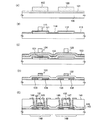
図1(A)に示すように、基板上に半導体膜101を成膜する。次に、半導体膜101上にレジスト、有機樹脂等で形成されるマスクパターン102、103を設ける。
As shown in FIG. 1A, a
基板100としては、ガラス基板、石英基板、セラミックス基板、プラスチック基板、ステンレス基板、可撓性基板等がある。また、SOI(Silicon on Insulator)基板を用いて半導体膜を形成しても良い。これらの基板を用いる際に、基板に接する下地膜(図示せず)を要する場合は適宜用いれば良い。本実施の形態では下地膜も含めて基板100と示す。
Examples of the
半導体膜101は、減圧熱CVD法、プラズマCVD法またはスパッタ法などの成膜法で形成される非晶質半導体膜を、レーザ結晶化法で結晶化した結晶性半導体を用いることが望ましい。また、上記成膜法で形成される非晶質半導体膜を固相成長法で結晶化した結晶性半導体膜、特許第3300153号公報に開示の技術を用いて形成した結晶性半導体膜を用いても良い。また、当該方法により形成した結晶性半導体膜に、レーザ照射をして結晶性を高めてもよい。また、シラン(SiH4)を原料として形成される微結晶半導体膜をレーザ結晶化した結晶性半導体膜等を用いても良い。更には、半導体膜として、微結晶半導体膜を用いても良い。
As the
半導体膜の半導体材料としては、シリコン(Si)、ゲルマニウム(Ge)、またシリコンゲルマニウム合金、炭化シリコン(炭化珪素)、ガリウム砒素などの化合物半導体材料を用いるこができる。 As a semiconductor material of the semiconductor film, a compound semiconductor material such as silicon (Si), germanium (Ge), a silicon germanium alloy, silicon carbide (silicon carbide), gallium arsenide, or the like can be used.
なお、レーザ結晶化の場合、レーザ結晶化の前に、レーザに対する半導体膜の耐性を高めるために、500℃、1時間の熱アニールを該半導体膜に対して行うことが望ましい。そして連続発振が可能な固体レーザを用い、基本波の第2高調波〜第4高調波のレーザ光を照射することで、大粒径の結晶を得ることができる。例えば、代表的には、Nd:YVO4レーザ(基本波1064nm)の第2高調波(532nm)や第3高調波(355nm)を用いるのが望ましい。具体的には、連続発振のYVO4レーザから射出されたレーザ光を非線形光学素子により高調波に変換し、出力数W以上のレーザ光を得る。そして、好ましくは光学系により照射面にて矩形状または楕円形状のレーザ光に成形して、半導体膜に照射する。このときのパワー密度は0.01〜100MW/cm2程度(好ましくは0.1〜10MW/cm2)である。そして、走査速度を10〜200cm/sec程度とし、照射する。 In the case of laser crystallization, it is desirable to perform thermal annealing on the semiconductor film at 500 ° C. for 1 hour before laser crystallization in order to increase the resistance of the semiconductor film to the laser. By using a solid-state laser capable of continuous oscillation and irradiating laser light of the second harmonic to the fourth harmonic of the fundamental wave, a crystal having a large grain size can be obtained. For example, typically, it is desirable to use the second harmonic (532 nm) or the third harmonic (355 nm) of an Nd: YVO 4 laser (fundamental wave 1064 nm). Specifically, laser light emitted from a continuous wave YVO 4 laser is converted into a harmonic by a non-linear optical element to obtain laser light having an output number of W or more. Then, it is preferably formed into a rectangular or elliptical laser beam on the irradiation surface by an optical system and irradiated onto the semiconductor film. Power density at this time is approximately 0.01 to 100 MW / cm 2 (preferably 0.1~10MW / cm 2). Then, irradiation is performed at a scanning speed of about 10 to 200 cm / sec.
なおレーザは、公知の連続発振の気体レーザもしくは固体レーザを用いることができる。気体レーザとして、Arレーザ、Krレーザなどがあり、固体レーザとして、YAGレーザ、YVO4レーザ、YLFレーザ、YAlO3レーザ、Y2O3レーザ、ガラスレーザ、ルビーレーザ、アレキサンドライトレーザ、Ti:サファイアレーザなどが挙げられる。 As the laser, a known continuous wave gas laser or solid-state laser can be used. Examples of gas lasers include Ar laser and Kr laser, and solid-state lasers include YAG laser, YVO 4 laser, YLF laser, YAlO 3 laser, Y 2 O 3 laser, glass laser, ruby laser, alexandrite laser, Ti: sapphire laser. Etc.
また、パルス発振のレーザ光の発振周波数を0.5MHz以上とし、通常用いられている数十Hz〜数百Hzの周波数帯よりも著しく高い周波数帯を用いてレーザ結晶化を行っても良い。パルス発振でレーザ光を照射して半導体膜を溶融してから半導体膜が完全に固化するまでの時間は数十nsec〜数百nsecと言われている。よって上記周波数帯を用いることで、半導体膜がレーザ光によって溶融してから固化するまでに、次のパルスのレーザ光を照射できる。したがって、半導体膜中において固液界面を連続的に移動させることができるので、走査方向に向かって連続的に成長した結晶粒を有する半導体膜が形成される。具体的には、含まれる結晶粒の走査方向における幅が10〜30μm、走査方向に対して垂直な方向における幅が1〜5μm程度の結晶粒の集合を形成することができる。該走査方向に沿って長く延びた単結晶の結晶粒を形成することで、少なくともTFTのチャネル方向には結晶粒界のほとんど存在しない半導体膜の形成が可能となる。 Further, the laser crystallization may be performed using a frequency band significantly higher than a frequency band of several tens to several hundreds Hz that is usually used with an oscillation frequency of pulsed laser light of 0.5 MHz or more. It is said that the time from melting a semiconductor film by irradiating laser light by pulse oscillation until the semiconductor film is completely solidified is several tens to several hundreds nsec. Therefore, by using the above frequency band, it is possible to irradiate the next pulse of laser light from when the semiconductor film is melted by the laser light to solidification. Accordingly, since the solid-liquid interface can be continuously moved in the semiconductor film, a semiconductor film having crystal grains continuously grown in the scanning direction is formed. Specifically, a set of crystal grains having a width of 10 to 30 μm in the scanning direction of the included crystal grains and a width of about 1 to 5 μm in a direction perpendicular to the scanning direction can be formed. By forming single crystal grains extending long along the scanning direction, it is possible to form a semiconductor film having almost no crystal grain boundaries in at least the channel direction of the TFT.
また、希ガスや窒素などの不活性ガス雰囲気中でレーザ光を照射するようにしても良い。これにより、レーザ光の照射により半導体表面の荒れを抑えることができ、界面準位密度のばらつきによって生じる閾値電圧のばらつきを抑えることができる。 Further, laser light may be irradiated in an inert gas atmosphere such as a rare gas or nitrogen. As a result, it is possible to suppress the roughness of the semiconductor surface by laser light irradiation, and to suppress the variation in threshold voltage caused by the variation in interface state density.
本実施の形態では、パルス発振のレーザ光を非晶質半導体膜に照射して、結晶性シリコン膜を形成する。この後、後に形成されるトランジスタのしきい値を制御するため、半導体膜にB2H6をドーピングしてチャネルドープを行ってもよい。 In this embodiment mode, a crystalline silicon film is formed by irradiating an amorphous semiconductor film with pulsed laser light. Thereafter, in order to control a threshold value of a transistor to be formed later, the semiconductor film may be doped with B 2 H 6 to perform channel doping.
マスクパターン102、103は公知のフォトリソグラフィ工程を用いてレジストマスクを形成する。また、所定の場所に材料を吐出することが可能なインクジェット法や液滴吐出法等により、有機樹脂、無機材料等の絶縁材料を吐出してマスクを形成することが可能である。また、印刷法を用いることも可能である。さらにはマスクパターン102、103の面積をより小さくすることで、メモリトランジスタ及びTFTが高集積化された半導体装置を作製することができる。
The
次に、図1(B)に示すように、マスクパターン102、103を用いて半導体膜101をエッチングして、第1半導体領域111及び第2半導体領域112を形成する。なお、第1半導体領域111は、後に形成される半導体メモリトランジスタの活性領域となり、第2半導体領域112は、後に形成されるTFTの活性領域となる。
Next, as shown in FIG. 1B, the
次に、マスクパターン102、103を除去した後、各半導体領域111、112及び基板100上に、第1絶縁膜113を成膜する。第1絶縁膜113は、膜厚1〜100nm、好ましくは1〜10nm、さらに好ましくは2〜5nmであることが望ましい。第1絶縁膜は、後にメモリトランジスタではトンネル酸化膜として、TFTではゲート絶縁膜の一部として機能する。このため、第1絶縁膜の膜厚が薄いほどトンネル電流が流れやすく、高速動作が可能となり好ましい。また、第1絶縁膜の膜厚が薄い程、低電圧でフローティングゲート電極に電荷を蓄積させることが可能である。この結果、後に形成される半導体装置の消費電力を低減することが可能である。
Next, after removing the
第1絶縁膜113の形成方法としては、GRTA(Gas Rapid Thermal Anneal)法、LRTA(Lamp Rapid Thermal Anneal)法等を用いて半導体領域表面を酸化し、熱酸化膜を形成することで、膜厚の薄い第1絶縁膜を形成することができる。また、この方法の他、CVD法、塗布法等を用いて形成してもよい。第1絶縁膜113としては、酸化珪素膜、窒化珪素膜で形成することができる。また、基板100側から酸化珪素膜及び窒化珪素膜や、酸化珪素膜、窒化珪素膜及び酸化珪素膜などの積層構造としてもよい。本実施の形態では、第1絶縁膜113として、酸化珪素膜、窒化珪素膜を積層させて形成する。
As a method for forming the first insulating
次に、第1絶縁膜113上に分散された(点在する)複数の導電性粒子又は半導体粒子(以下、分散粒子と示す。)114を形成する。分散粒子の作製方法としては、スパッタリング法、プラズマCVD法、減圧CVD(LPCVD)法、蒸着法、液滴吐出法等の公知の手法を用いることができる。プラズマCVD法、減圧CVD(LPCVD)法、蒸着法、液滴吐出法等で分散粒子を形成すると、分散粒子を形成時の第1絶縁膜への衝撃を低減することが可能であるため、第1絶縁膜の欠陥の発生を抑制することが可能である。この結果、信頼性の高い半導体装置を作製することが可能である。また、導電性膜又は半導体膜を上記方法により成膜した後、所望の形状にエッチングして分散粒子を形成することができる。分散粒子の大きさは、0.1〜10nm、好ましくは2〜5nmである。また、導電性粒子の材料としては、金、銀、銅、パラジウム、白金、コバルト、タングステン、ニッケル等を用いることができる。半導体粒子の材料としては、シリコン(Si)、ゲルマニウム(Ge)、またシリコンゲルマニウム合金等を用いることができる。ここでは、分散粒子114としてシリコン微粒子を形成する。
Next, a plurality of conductive particles or semiconductor particles (hereinafter, referred to as dispersed particles) 114 dispersed (scattered) over the first insulating
なお、ここでは、分散粒子は一部粒子同士が凝集していてもよい。 Here, some of the dispersed particles may be aggregated.
次に、分散粒子114上にマスクパターン115を形成する。ここでは、マスクパターン115は、後にメモリトランジスタとなる第1半導体領域111上に形成する。
Next, a
次に、図1(C)に示すように、マスクパターン115を用いて分散粒子114の一部をエッチングして、フローティングゲート電極121を形成する。分散粒子114の除去方法としては、ドライエッチング法、ウエットエッチング法等公知のエッチング方法を用いることが可能である。なお、分散粒子114が形成されている第1絶縁膜113の膜厚が薄い場合にドライエッチングを用いると、プラズマ衝撃により第1絶縁膜に欠陥が生じる可能性がある。このため、ウエットエッチングで除去を行うことが好ましい。ここでは、NMD3溶液(テトラメチルアンモニウムハイドロオキサイドを0.2〜0.5%含む水溶液)等を用いたウエットエッチング法により、分散粒子114であるシリコン微結晶を選択的に除去する。
Next, as shown in FIG. 1C, part of the dispersed
フローティングゲート電極は分散された粒子で形成されている。このため、トンネル酸化膜として機能する第1絶縁膜に欠陥があった場合でも、フローティングゲート電極に蓄積した電荷すべてが、欠陥から半導体領域に流れ出ることを回避することができる。この結果、信頼性の高い半導体メモリトランジスタを形成することができる。 The floating gate electrode is formed of dispersed particles. For this reason, even when the first insulating film functioning as the tunnel oxide film has a defect, it is possible to prevent all charges accumulated in the floating gate electrode from flowing out of the defect into the semiconductor region. As a result, a highly reliable semiconductor memory transistor can be formed.
次に、マスクパターン115を除去した後、フローティングゲート電極121及び第1絶縁膜113上に第2絶縁膜122を成膜する。第2絶縁膜113は、膜厚1〜100nm、好ましくは10〜70nm、さらに好ましくは10〜30nmであることが望ましい。第2絶縁膜122は、メモリトランジスタにおいてフローティングゲート電極121と後に形成されるゲート電極との絶縁性を保つ必要がある。このため、これらの間でリーク電流が増加しない程度の膜厚とすることが好ましい。第2絶縁膜122は、第1絶縁膜113と同様に、酸化珪素膜、窒化珪素膜で形成することができる。また、基板100側から酸化珪素膜及び窒化珪素膜の2層や、酸化珪素膜、窒化珪素膜、及び酸化珪素膜の3層など積層構造としてもよい。なお、半導体領域に接して酸化珪素膜を形成すると、ゲート絶縁膜と半導体領域との界面準位が低くなるため好ましい。ここでは、第2絶縁膜122として、膜厚10nmの酸化珪素膜と膜厚20nmの窒化珪素膜の積層構造で形成する。
Next, after removing the
この後、第2絶縁膜を成膜の後、図1(B)に示すように、分散粒子及びそれを覆うマスクパターンを形成して、第2フローティングゲート電極を形成しても良い。更には、同様の工程を繰り返して、複数に積層されたフローティングゲート電極を形成しても良い。 Thereafter, after forming the second insulating film, as shown in FIG. 1B, the dispersed particles and a mask pattern covering the dispersed particles may be formed to form the second floating gate electrode. Furthermore, the same process may be repeated to form a plurality of stacked floating gate electrodes.
次に、第2絶縁膜122上に第1導電膜123を成膜する。第1導電膜は、スパッタリング法、蒸着法、CVD法等の公知の手法により形成することができる。また、第1導電膜は、タンタル(Ta)、タングステン(W)、チタン(Ti)、モリブデン(Mo)、アルミニウム(Al)、銅(Cu)、クロム(Cr)、ネオジム(Nd)から選ばれた元素、またはこれらの元素を主成分とする合金材料若しくは化合物材料を用いて形成することができる。また不純物元素が添加された半導体膜を用いて形成することができる。
Next, a first
なお、第1導電膜123の材料としては、第2絶縁膜122と比較してエッチング速度が十分大きなものを用いることが望ましい。この結果、第1導電膜のエッチングの際に露出される第2絶縁膜122のオーバーエッチングを防ぐことができる。
Note that as the material of the first
次に、第1導電膜123上にマスクパターン124、125を形成する。マスクパターン124、125の形成方法は、マスクパターン102、103と同様の手法を適宜用いることができる。また、上記手法により形成したパターンを、アッシング等によりスリミングしてマスクパターンの幅を細くしてもよい。この結果、後に形成されるゲート電極のチャネル長方向の幅の細い短チャネル構造のTFTを形成することが可能であり、高速動作が可能なTFTを形成することが可能である。なお、このマスクパターン124、125は、後にゲート電極を形成するためのマスクパターン124、125である。このため、液滴吐出法を用いてゲート電極を形成する場合は、マスクパターン124、125を設けなくともよい。
Next,
次に、図1(D)に示すように、マスクパターン124、125を用いて第1導電膜をエッチングしてゲート電極131、132を形成する。ゲート電極の幅は0.2〜1.5μm、好ましくは0.2〜0.7μmとする。ゲート電極の幅を当該範囲内に設定することにより、後にチャネル長の短いメモリトランジスタ及びTFTを形成することが可能であり、高速動作が可能な半導体装置を作製することが可能である。
Next, as shown in FIG. 1D, the first conductive film is etched using the
次に、マスクパターン124、125及びゲート電極131、132をマスクとして第1半導体領域111、第2半導体領域112それぞれに、n型又はp型を付与する不純物元素を添加する。次に、マスクパターン124、125を除去した後、絶縁膜を成膜し、加熱処理、GRTA法、LRTA法等により、不純物元素の活性化を行い、ソース領域及びドレイン領域133〜136を形成する。この後、第2絶縁膜及びゲート電極上に窒化珪素膜からなる無機絶縁膜を設けて、加熱処理を行っても良い。この無機絶縁膜を、膜中に水素を含ませる条件で成膜し、加熱処理を行うことで、各半導体領域のダングリングボンドの終端を水素化することが可能である。
Next, an impurity element imparting n-type or p-type is added to each of the
次に、図1(E)に示すように、第2絶縁膜122上に層間絶縁膜として機能する第3絶縁膜を形成する。第3絶縁膜は、ポリイミド、アクリル、ポリアミド等の耐熱性を有する有機樹脂を用いることができる。また上記有機樹脂の他に、低誘電率材料(low−k材料)、シロキサン系材料を出発材料として形成されたSi−O−Si結合を含む樹脂(以下、シロキサン系樹脂と呼ぶ)等を用いることができる。シロキサン系樹脂は、置換基として水素の他、アルキル基、または芳香族炭化水素等の有機基のうち少なくとも1種を有していても良い。また、フルオロ基を有してもよい。第3絶縁膜の形成には、その材料に応じて、スピンコート、ディップ、スプレー塗布、液滴吐出法、インクジェット法、スクリーン印刷、オフセット印刷等、ドクターナイフ、ロールコーター、カーテンコーター、ナイフコーター、CVD法、蒸着法等を採用することができる。また、無機材料を用いてもよく、その際には、酸化珪素、窒化珪素、酸窒化珪素、PSG(リンガラス)、BPSG(リンボロンガラス)、アルミナ膜等を用いることができる。なお、これらの絶縁膜を積層させて、第3絶縁膜を形成しても良い。ここでは、アクリルを塗布し焼成して第3絶縁膜を形成する。
Next, as illustrated in FIG. 1E, a third insulating film functioning as an interlayer insulating film is formed over the second
次に、フォトリソグラフィ工程及びエッチング工程により第3絶縁膜の一部、第2絶縁膜122、及び第1絶縁膜113の一部をエッチングしてコンタクトホールを形成すると共に、ソース領域及びドレイン領域の一部を露出する。このとき、エッチングされた第3絶縁膜を第3絶縁層141、エッチングされた第2絶縁膜を第2絶縁層142、エッチングされた第1絶縁膜を第1絶縁層143と示す。なお、ここでは、第3絶縁層141は、表面が平坦な絶縁膜が図示されているが、平坦でなくとも良い。
Next, a part of the third insulating film, the second
次に、ソース領域及びドレイン領域に接続するソース電極及びドレイン電極144〜147を形成する。ソース電極及びドレイン電極は、PVD法(Physical Vapor Deposition)、CVD法(Chemical Vapor Deposition)、蒸着法等により導電膜を成膜した後、所望の形状にエッチングして形成することができる。また、液滴吐出法、印刷法、電界メッキ法等により、所定の場所に選択的に導電層を形成することができる。更にはリフロー法、ダマシン法を用いても良い。ソース領域及びドレイン領域の材料は、Ag、Au、Cu、Ni、Pt、Pd、Ir、Rh、W、Al、Ta、Mo、Cd、Zn、Fe、Ti、Si、Ge、Zr、Ba等の金属又はその合金、若しくはその金属窒化物を用いて形成する。また、これらの積層構造としても良い。
Next, source and drain
ここで、ゲート電極131とフローティングゲート電極121との端部の位置関係について図27を用いて説明する。図27において、ゲート電極131の幅をそれぞれL1〜L3と示し、フローティングゲート電極の幅をD1〜D3と示す。図27(A)においては、ゲート電極131の幅L1とフローティングゲート電極121の幅D1とが等しい構造、即ちゲート電極の端部とフローティングゲート電極の端部それぞれが、概略一致しているメモリトランジスタを示す。
Here, the positional relationship between the end portions of the
図27(B)においては、ゲート電極131の幅L2よりもフローティングゲート電極121の幅D2の方が大きい、即ちフローティングゲート電極の両端部がゲート電極の両端部の外側に設けられている構造のメモリトランジスタを示す。このとき、ゲート電極131よりも外側に設けられたフローティングゲート電極152は、電荷蓄積層としては機能しない。従って、フローティングゲート電極121の両端部がゲート電極131の両端部より外側に設けられる構造と、等しく重なる構造とは、製造工程や微細化に有利となるように、適宜選択すればよい。
In FIG. 27B, the width D2 of the floating
図27(C)においては、ゲート電極131の幅L3よりもフローティングゲート電極121の幅D3が小さい構造のメモリトランジスタを示す。この場合、いわゆるスプリットゲート電極構造のメモリトランジスタとなる。スプリットゲート電極構造とは、一つの半導体領域111及びゲート電極131で、メモリトランジスタを選択する選択用トランジスタと、メモリトランジスタとを構成する素子をいう。これは図27(D)に示すように、一組の信号線160、161でメモリトランジスタ162と選択用のトランジスタ163とを制御する構成である。このような構成は、メモリトランジスタが過消去状態(閾値電圧よりも負の状態)になっても、選択用のトランジスタ163によりメモリセルの選択性を保つことができるため、動作マージンに優れる。なお、図27(C)では、フローティングゲート電極の一方の端がゲート電極の端と一致する構成を示したが、この構造に限られない。フローティングゲート電極121の両端が、ゲート電極131の両端の内側に設けられていても良い。
FIG. 27C shows a memory transistor having a structure in which the width D3 of the floating
また、以下の方法により、図1に示す基板100からのメモリトランジスタ148及びTFT149を剥離することが可能である。剥離方法としては、(1)基板100として、300〜500度程度の耐熱性を有する基板を用い、当該基板100とメモリトランジスタ148及びTFT149との間に金属酸化膜を設け、当該金属酸化膜を結晶化により脆弱化して、当該メモリトランジスタ148及びTFT149を剥離する方法、(2)基板100とメモリトランジスタ148及びTFT149の間に水素を含む非晶質珪素膜を設け、レーザ光を照射、またはガス・溶液でのエッチングにより当該非晶質珪素膜を除去することで、当該メモリトランジスタ148及びTFT149を剥離する方法、(3)メモリトランジスタ148及びTFT149が形成された基板100を機械的に削除する、又は溶液やCF3等のガスによるエッチングで除去することで、当該メモリトランジスタ148及びTFT149を切り離す方法等が挙げられる。また、剥離したメモリトランジスタ148及びTFT149のフレキシブル基板への貼り付けは、市販の接着剤を用いればよく、例えば、エポキシ樹脂系接着剤や樹脂添加剤等の接着材を用いればよい。
Further, the
上記のように、剥離したメモリトランジスタ148及びTFT149をフレキシブル基板に貼り合わせると、厚さが薄く、軽く、落下しても割れにくい半導体装置を提供することができる。また、フレキシブル基板は可撓性を有するため、曲面や異形の形状上に貼り合わせることが可能となり、多種多様の用途が実現する。また、基板100を再利用すれば、安価な半導体装置の提供が可能である。
As described above, when the peeled
以上の工程により、第1半導体領域111、トンネル酸化膜として機能する第1絶縁層143、フローティングゲート電極121、第2絶縁層142、及びゲート電極131で構成されるメモリトランジスタ148と、第2半導体領域112、ゲート絶縁膜として機能する第1絶縁層143及び第2絶縁層142、並びにゲート電極132で構成されるTFT149とを、同一基板上に有する半導体装置を形成することができる。なお、TFT149は、メモリトランジスタを選択するデコーダ回路、書き込み・読み出し回路等の周辺回路、CPU、DRAM、画像処理回路、音声処理回路等の機能回路、バッファ回路、シフトレジスタ回路、レベルシフタ回路及びサンプリング回路等の駆動回路等に適宜用いることができる。
Through the above process, the
本実施の形態で形成される半導体装置は、結晶性シリコン膜を用いて形成することが可能であるため、高価な単結晶半導体基板を用いず作製することができる。このため、コスト削減が可能である。また、基板100として大面積基板を用い、上記の工程により複数の半導体装置の回路パターンを形成し、最後に矩形状又は短冊状に分割して、個々の半導体装置を取り出すことによって、大量の半導体装置を形成することが可能である。この結果、低コスト化が可能である。さらに本実施の形態で作製したメモリトランジスタ148及びTFT149を剥離し、フレキシブル基板に接着することにより、薄型の半導体装置の作製が可能である。
Since the semiconductor device formed in this embodiment can be formed using a crystalline silicon film, it can be manufactured without using an expensive single crystal semiconductor substrate. For this reason, cost reduction is possible. In addition, a large-area substrate is used as the
また、メモリトランジスタのフローティングゲート電極に分散された粒子を用いているため、トンネル酸化膜の欠陥による蓄積電荷の流出を回避することができる。このため、信頼性の高い半導体装置を形成することができる。 In addition, since particles dispersed in the floating gate electrode of the memory transistor are used, outflow of accumulated charges due to defects in the tunnel oxide film can be avoided. For this reason, a highly reliable semiconductor device can be formed.
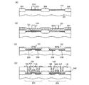
(実施の形態2)
本実施の形態では、実施の形態1においてフローティングゲート電極とゲート電極との端部が概略一致するメモリトランジスタを有する半導体装置の作製方法について図29を用いて説明する。
(Embodiment 2)
In this embodiment, a method for manufacturing a semiconductor device including a memory transistor in which end portions of a floating gate electrode and a gate electrode are substantially the same as those in
図29(A)に示すように、実施の形態1と同様に第1絶縁膜113上に分散粒子114を形成する。次に、マスクパターン155を形成する。ここで、マスクパターン155は、少なくともTFTの活性領域となる第2半導体領域112を覆わず、メモリトランジスタの活性領域となる第1半導体領域111を覆っていれば良い。
As shown in FIG. 29A, dispersed
次に、図29(B)に示すように、第2絶縁膜122及び第1導電膜123を成膜する。次に、マスクパターン124、125を形成する。
Next, as shown in FIG. 29B, a second
次に図29(C)に示すように、マスクパターン124、125を用いて第1導電膜123、第2絶縁膜122、及び残存した分散粒子151の一部をエッチングして除去し、ゲート電極131、132、第2絶縁層165、166、分散粒子で形成されるフローティングゲート電極167を形成する。ここでは、第1導電膜123及び第2絶縁膜122を、ドライエッチングによりエッチングする。この後、マスクパターン124、125を除去せず、残存した分散粒子151の一部をウエットエッチングによりエッチングする。この工程により、ゲート電極131とフローティングゲート電極167とが自己整合的に形成される。
Next, as shown in FIG. 29C, the first
この後、実施の形態1と同様の工程により、メモリトランジスタ178及びTFT179を形成することができる。
Thereafter, the
以上の工程により、第1半導体領域111、トンネル酸化膜として機能する第1絶縁層143、フローティングゲート電極167、第2絶縁層165、及びゲート電極131で構成されるメモリトランジスタ178と、第2半導体領域112、ゲート絶縁膜として機能する第1絶縁層143及び第2絶縁層166、並びにゲート電極132で構成されるTFT179とを、同一基板上に有する半導体装置を形成することができる。
Through the above process, the
(実施の形態3)
本実施の形態では、単結晶半導体基板を用いてメモリトランジスタとMOSトランジスタとを、同一基板上に形成する工程を、図2を用いて説明する。
(Embodiment 3)
In this embodiment, a process of forming a memory transistor and a MOS transistor over the same substrate using a single crystal semiconductor substrate will be described with reference to FIGS.
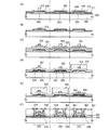
図2(A)に示すように、基板201に素子分離領域202〜204を形成する。基板201は、単結晶半導体基板又は化合物半導体基板であり、代表的には、n型またはp型の単結晶シリコン基板、GaAs基板、InP基板、GaN基板、SiC基板、サファイヤ基板、又はZnSe基板等が挙げられる。また、SOI基板(Silicon On Insulator)を用いこともできる。本実施の形態では、基板201として、単結晶シリコン基板を用いる。素子分離領域202〜204は、公知の選択酸化法(LOCOS(Local Oxidation of Silicon)法)又はトレンチ分離法等を適宜用いることができる。ここでは、素子分離領域202〜204としては、LOCOS法によりシリコン基板の一部を酸化して、酸化珪素膜を形成する。この後、ウエルイオン注入、チャネルストップイオン注入、閾値電圧調整イオン注入を適宜行う。
As illustrated in FIG. 2A,
次に、基板201の表面を洗浄して、基板201表面を露出する。この後、公知の手法により第1絶縁膜211を形成する。第1絶縁膜はメモリトランジスタのトンネル酸化膜として機能するため、膜厚は薄いことが好ましい。膜厚が薄いと、低い電圧でフローティングゲート電極に電荷を蓄積することが可能であり、低消費電力である半導体装置を形成することができる。ここでは、第1絶縁膜211は、熱酸化法により酸化珪素膜を形成する。
Next, the surface of the
次に、実施の形態1と同様に第1絶縁膜211上に分散粒子114を形成する。次に、後にメモリトランジスタが形成される領域にマスクパターン213を形成する。
Next, the dispersed
次に分散粒子114の一部をエッチングして、図2(B)に示すように、フローティングゲート電極121を形成する。次に、素子分離領域202〜204、第1絶縁膜211、及びフローティングゲート電極121上に第2絶縁膜222を成膜する。なお、実施の形態2と同様の工程を用いてフローティングゲート電極を形成しても良い。次に、第2絶縁膜222上に第1導電膜223を成膜する。第2絶縁膜222及び第1導電膜223はそれぞれ、実施の形態1の第2絶縁膜122及び第1導電膜123と同様の材料及び成膜方法により形成することができる。次に、第1導電膜223上にマスクパターン124、125を形成する。
Next, part of the dispersed
次に、マスクパターン124、125を用いて第1導電膜をエッチングして、図2(C)に示すように、ゲート電極131、132を形成する。次に、マスクパターン124、125及びゲート電極131、132をマスクとして、基板201に自己整合的に不純物元素を添加する。次に、マスクパターン124、125を除去した後、加熱処理、GRTA法、LRTA法等により、不純物元素の活性化を行い、ソース領域及びドレイン領域233〜236を形成する。
Next, the first conductive film is etched using the
次に、図2(D)に示すように、第2絶縁膜222上に第3絶縁膜を形成する。この後、第3絶縁膜の一部、第2絶縁膜222、及び第1絶縁膜211の一部をエッチングしてコンタクトホールを形成すると共に、ソース領域及びドレイン領域の一部を露出する。ここで、エッチングされた第3絶縁膜を第3絶縁層141、エッチングされた第2絶縁膜を第2絶縁層242、エッチングされた第1絶縁膜を第1絶縁層243と示す。この後、ソース領域及びドレイン領域に接続するソース電極及びドレイン電極144〜147を形成する。
Next, as illustrated in FIG. 2D, a third insulating film is formed over the second
以上の工程により、半導体単結晶を用いた基板201、トンネル酸化膜として機能する第1絶縁層243、フローティングゲート電極121、第2絶縁層242、及びゲート電極131で構成されるメモリトランジスタ251と、半導体単結晶を用いた基板201、ゲート絶縁膜として機能する第1絶縁層243及び第2絶縁層242、並びにゲート電極132で構成されるMOSトランジスタ252とを、同一基板上に有する半導体装置を形成することができる。なお、MOSトランジスタ252は、メモリトランジスタを選択するデコーダ回路、書き込み・読み出し回路等の周辺回路、CPU、DRAM、画像処理回路、音声処理回路等の機能回路、バッファ回路、シフトレジスタ回路、レベルシフタ回路及びサンプリング回路等の駆動回路等に適宜用いることができる。
Through the above steps, the
また、基板201としてSOI基板(Silicon On Insulator)を用い、実施の形態1で示すようなシリコン基板との酸化絶縁膜を用いた剥離方法により、メモリトランジスタ及びMOSトランジスタを剥離することができる。また、当該剥離したメモリトランジスタ及びMOSトランジスタを実施の形態1と同様にフレキシブル基板に接着することにより、半導体装置の薄型化が可能である。
Further, an SOI substrate (Silicon On Insulator) is used as the
また、メモリトランジスタのフローティングゲート電極として分散された粒子を用いているため、トンネル酸化膜の欠陥による蓄積電荷の流出を回避することができる。このため、信頼性の高い半導体装置を形成することができる。 Further, since dispersed particles are used as the floating gate electrode of the memory transistor, it is possible to avoid the outflow of accumulated charges due to a defect in the tunnel oxide film. For this reason, a highly reliable semiconductor device can be formed.
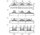
本実施例では、メモリトランジスタとCMOS回路を同一基板に有する半導体装置の作製工程について、図3を用いて説明する。本実施例において、メモリトランジスタ及びTFTはシングルドレイン構造である。 In this embodiment, a manufacturing process of a semiconductor device including a memory transistor and a CMOS circuit over the same substrate will be described with reference to FIGS. In this embodiment, the memory transistor and the TFT have a single drain structure.
図3(A)に示すように、ガラス基板300上に第1絶縁膜301を成膜する。第1絶縁膜301は、基板からの不純物元素が後に形成される半導体領域に拡散するのを防止するためのブロッキング膜として機能する。このため、第1絶縁膜301としては、酸化珪素膜、窒化珪素膜または酸化窒化珪素膜などの絶縁膜からなる下地膜を形成する。さらには、酸化珪素膜と窒化珪素膜とを連続的に積層して成膜してもよい。
As shown in FIG. 3A, a first
次に、第1絶縁膜301上にアモルファスシリコン膜を成膜し、アモルファスシリコン膜に80MHzの周波数を有するパルス発振のレーザ光を照射して結晶性シリコン膜を形成する。次に、フォトリソグラフィ工程及びエッチング工程により結晶性シリコン膜を所望の形状にエッチングして、第1半導体領域303、第2半導体領域304、及び第3半導体領域305を形成する。なお、第1半導体領域303は後のメモリトランジスタの活性領域、第2半導体領域304は後のnチャネル型TFTの活性領域、第3半導体領域305は後のpチャネル型TFTの活性領域として機能する。
Next, an amorphous silicon film is formed over the first insulating
次に、第1乃至第3半導体領域303〜305の表面に形成された自然酸化膜を除去した後、ヒドロキシラジカルを含むオゾン水に数十秒〜数分曝して、半導体領域303〜305表面に酸化珪素膜を形成する。この後、GRTA(Gas Rapid Thermal Anneal)法、LRTA(Lamp Rapid Thermal Anneal)法により酸化シリコン膜をより緻密化し、膜厚1〜2nmの第2絶縁膜306〜308を形成する。この方法により、短時間且つ高温で処理することが可能であるため、基板を伸縮させずとも緻密且つ膜厚の薄い第2絶縁膜を形成することができる。次に、第2絶縁膜306〜308及びガラス基板300上に第3絶縁膜309を成膜する。ここでは、第3絶縁膜309として、膜厚1〜5nmの窒化珪素膜又は窒化酸化珪素膜(SiNO(N>O))を成膜する。
Next, after removing the natural oxide film formed on the surfaces of the first to
次に、第3絶縁膜309上に分散粒子としてシリコン微粒子310をプラズマCVD法により形成する。次にシリコン微粒子310及び第3絶縁膜309上に第4絶縁膜311を成膜する。第4絶縁膜311としては、プラズマCVD法により膜厚10〜20nmの窒化珪素膜、又は窒化酸化珪素膜(SiNO(N>O)を成膜する。次に、フォトリソグラフィ工程によりマスクパターン312を第1半導体領域303上に形成する。
Next, silicon
次に、図3(B)に示すように、マスクパターン312を用いて第4絶縁膜及びシリコン微粒子310の一部をエッチングしてフローティングゲート電極を有する絶縁層313を形成する。ここでは、ドライエッチングにより第4絶縁膜をエッチングして、シリコン微粒子310を露出した後、NMD3溶液(テトラメチルアンモニウムハイドロオキサイドを0.2〜0.5%含む水溶液)等を用いて、シリコン微粒子をエッチングする。ここで、フローティングゲート電極は、残存したシリコン微粒子で形成されている。
Next, as shown in FIG. 3B, the fourth insulating film and part of the silicon
次に、図3(C)に示すように、第4絶縁膜及びフローティングゲート電極を有する絶縁層313上に第5絶縁膜321を成膜する。第5絶縁膜321としては、プラズマCVD法により膜厚20〜50nmの酸化珪素膜、又は酸化窒化珪素(SiON(O>N)を成膜する。
Next, as illustrated in FIG. 3C, a fifth
次に、第1導電膜322を成膜する。ここでは第1導電膜322としてスパッタリング法により膜厚400nmのタングステン膜を成膜する。次に、第1半導体領域乃至第3半導体領域303〜305上にフォトリソグラフィ工程により、マスクパターン323〜325を形成する。
Next, a first
次に、図3(D)に示すように、マスクパターン323〜325を用いて第1導電膜322をエッチングしてゲート電極331〜333を形成する。このときのゲート電極の幅を0.2〜1.5nm、好ましくは0.2〜0.7nmとする。次に、マスクパターン323〜325を除去した後、新たに第3半導体領域305上にマスクパターン334を形成する。
Next, as illustrated in FIG. 3D, the first
次に、第1半導体領域303及び第2半導体領域304にゲート電極331、332をマスクとして不純物元素を添加する。ここでは、n型を呈する不純物元素であるリン(P)を各半導体領域に添加し、n型を呈するソース領域及びドレイン領域335〜338を形成する。
Next, an impurity element is added to the
次に、図3(E)に示すように、マスクパターン334を除去した後、フォトリソグラフィ工程により、第1半導体領域303及び第2半導体領域304上にマスクパターン341、342を形成する。次に、ゲート電極325をマスクとして第3半導体領域305に不純物元素を添加する。ここでは、p型を呈する不純物元素であるボロン(B)を半導体領域に添加し、p型を呈するソース領域及びドレイン領域343、344を形成する。次に、マスクパターン341、342を除去した後、加熱してソース領域及びドレイン領域の不純物元素の活性化を行う。この後、第5絶縁膜321上に水素を含む絶縁膜を成膜し、加熱して、半導体領域表面の水素化を行ってもよい。
Next, as shown in FIG. 3E, after the
次に、図3(F)に示すように、第5絶縁膜321上に層間絶縁膜として機能する第6絶縁膜を成膜する。ここでは、シロキサン系樹脂を塗布し、焼成して第6絶縁膜を形成する。次に、第6絶縁膜、第5絶縁膜、第3絶縁膜、及び第2絶縁膜をエッチングしてコンタクトホールを形成すると共に、ソース領域及びドレイン領域335〜338、343、344の一部を露出する。エッチングされた第6絶縁膜を第6絶縁層351、エッチングされた第5絶縁膜を第5絶縁層352、及びエッチングされた第3絶縁膜第3絶縁層353と示す。また、エッチングされた第2絶縁膜を第2絶縁層354〜356と示す。次に、スパッタリング法によりチタン膜、アルミニウムシリコン合金膜、及びチタン膜を積層成膜した後、フォトリソグラフィ工程及びエッチング工程を用いてソース電極及びドレイン電極357〜362を形成する。
Next, as illustrated in FIG. 3F, a sixth insulating film functioning as an interlayer insulating film is formed over the fifth insulating
以上の工程により、また、第1半導体領域303、トンネル酸化膜として機能する第2絶縁層354及び第3絶縁層353、フローティングゲート電極を有する絶縁層313、第5絶縁層352、及びゲート電極331で構成されるメモリトランジスタ371を形成することができる。また、第2半導体領域304、ゲート絶縁膜として機能する第2絶縁層355、第3絶縁層353、及び第5絶縁層352、並びにゲート電極332で構成されるnチャネル型TFT372を形成することができる。また、第3半導体領域305、ゲート絶縁膜として機能する第2絶縁層356、第3絶縁層353、及び第5絶縁層352、並びにゲート電極333で構成されるpチャネル型TFT373を形成することができる。更には、シングルドレイン構造のメモリトランジスタ371、nチャネル型TFT372、及びpチャネル型TFT373を、同一基板上に有する半導体装置を形成することができる。
Through the above steps, the
また、本実施例は、実施の形態1〜3それぞれと組み合わせて用いることが可能である。 Further, this example can be used in combination with each of the first to third embodiments.
本実施例では、メモリトランジスタとCMOS回路を同一基板に有する半導体装置の作製工程について図3及び図4を用いて説明する。本実施例において、メモリトランジスタ及びTFTは、サイドウォール(側壁スペーサ)及び該領域に覆われた低濃度不純物領域(LDD((Light Doped Drain)領域と示す。)を有する。 In this embodiment, a manufacturing process of a semiconductor device having a memory transistor and a CMOS circuit on the same substrate will be described with reference to FIGS. In this embodiment, the memory transistor and the TFT have a sidewall (side wall spacer) and a low-concentration impurity region (LDD (referred to as a Light Doped Drain) region) covered with the region.
本実施例では、ゲート電極を形成する工程までは、実施例1と同様であるため、それ以降の工程について説明する。実施例1の工程にしたがって図3(D)に示すようにメモリ
トランジスタ、nチャネル型TFT及びpチャネル型TFTのゲート電極331〜333を形成する。次に、図4(A)に示すように、メモリトランジスタ及びnチャネル型TFTの半導体領域(第1半導体領域303及び第2半導体領域304)に、n型を呈する不純物元素であるリン(P)を添加し、n型を呈する第1低濃度不純物領域(以下、第1n型不純物領域と示す。)401〜404を形成する。次に、pチャネル型TFTの半導体領域(第3半導体領域305)にp型を呈する不純物元素であるボロン(B)を半導体領域に添加し、p型を呈する第1低濃度不純物領域(以下、第1p型不純物領域と示す。)405、406を形成する。
In this example, the process up to the step of forming the gate electrode is the same as that of Example 1, and the subsequent processes will be described. As shown in FIG. 3D,
次に、ゲート電極331〜333及び第5絶縁膜321上に第6絶縁膜410を成膜する。第6絶縁膜としては、CVD法により酸化珪素膜を成膜する。
Next, a sixth
次に、RIE(Reactive ion etching:反応性イオンエッチング)法により第6絶縁膜410を異方性エッチングして、図4(B)に示すように、サイドウォール(側壁スペーサ)411〜413を形成する。このとき、絶縁膜の材料によって、第2乃至第5絶縁膜の一部又は全部もエッチングされる。ここでは、第1半導体領域〜第4半導体領域をエッチングストッパーとして機能し、第2乃至第5絶縁膜がエッチングされる。ここで、エッチングされた第2絶縁膜407〜409をそれぞれ第2絶縁層416a〜416c、エッチングされた第3絶縁膜321をそれぞれ第3絶縁層415a〜415c、エッチングされた第5絶縁膜410をそれぞれ第2絶縁層414a〜414cと示す。
Next, the sixth
次に、図4(C)に示すように、フォトリソグラフィ工程により、後に形成されるpチャネル型TFTの半導体領域である第3半導体領域305を覆うマスクパターン421を形成する。次に、第1半導体領域303及び第2半導体領域304に、n型を呈する不純物元素であるリン(P)を添加し、n型を呈する高濃度不純物領域(ソース領域及びドレイン領域)422〜425を形成する。このとき、サイドウォールに覆われたn型を呈する第1低濃度不純物領域(以下、第2n型不純物領域(LDD領域))426〜429も形成される。このとき、第2n型不純物領域426〜429の幅は、0.01〜0.3μmであることが好ましい。この後、マスクパターン421を除去する。なお、第2n型不純物領域は低濃度不純物領域である。
Next, as shown in FIG. 4C, a
次に、図4(D)に示すように、フォトリソグラフィ工程により、第1半導体領域303及び第2半導体領域304、それぞれを覆うマスクパターン431、432を形成する。次に、第3半導体領域305に、p型を呈する不純物元素であるボロン(B)を半導体領域に添加し、p型を呈する高濃度不純物領域(ソース領域及びドレイン領域)422〜425を形成する。このとき、サイドウォールに覆われた第1p型不純物領域(以下、第2p型不純物領域(LDD領域))428、429も形成される。このとき、第2p型不純物領域428、429の幅は、0.01〜0.3μmであることが好ましい。次に、マスクパターン431、432を除去した後、加熱して不純物元素の活性化を行う。
Next, as shown in FIG. 4D,
次に、層間絶縁膜として機能する第7絶縁膜を成膜した後、実施例1と同様に、第7絶縁膜をエッチングして、コンタクトホールを形成すると共に、ソース領域及びドレイン領域422〜425、433、434の一部を露出する。第7絶縁膜は、実施例1の第6絶縁膜と同様の材料及び手法により形成する。エッチングされた第7絶縁膜を第7絶縁層451と示す。この後、実施例1と同様にソース電極及びドレイン電極357〜362を形成する。
Next, after forming a seventh insulating film functioning as an interlayer insulating film, the seventh insulating film is etched to form contact holes and source and drain
以上の工程により、第1半導体領域303、トンネル酸化膜として機能する第2絶縁層416a及び第3絶縁層415a、フローティングゲート電極を有する絶縁層313、第5絶縁層414a、ゲート電極331、並びにサイドウォール411を有するメモリトランジスタ441を形成することができる。
Through the above steps, the
また、第2半導体領域304、ゲート絶縁膜として機能する第2絶縁層416b、第3絶縁層415b、及び第5絶縁層414b、ゲート電極332、並びにサイドウォール412で構成されるnチャネル型TFT429を形成することができる。
In addition, an n-
また、第3半導体領域305、ゲート絶縁膜として機能する第2絶縁層416c、第3絶縁層415c、及び第5絶縁層414c、ゲート電極333、並びにサイドウォール413で構成されるpチャネル型TFT443を形成することができる。更には、メモリトランジスタ441、nチャネル型TFT442、及びpチャネル型TFT443を、同一基板上に有する半導体装置を形成することができる。
Further, a p-
また、本実施例で形成したメモリトランジスタ及びTFTは、サイドウォール構造であるため、サブミクロン構造のメモリトランジスタ及びTFTにおいてもLDD領域を形成することが可能である。また、LDD領域を有するため、ドレイン近傍の電界を緩和してホットキャリア注入による劣化を防ぐ効果、及びオフ電流を低減する効果がある。この結果、信頼性の高い半導体装置を作製することが可能である。 In addition, since the memory transistor and the TFT formed in this embodiment have a sidewall structure, an LDD region can be formed even in a memory transistor and a TFT having a submicron structure. In addition, since the LDD region is provided, there is an effect of relaxing an electric field in the vicinity of the drain to prevent deterioration due to hot carrier injection and an effect of reducing off-current. As a result, a highly reliable semiconductor device can be manufactured.
また、本実施例は、実施の形態1〜3、実施例1それぞれと組み合わせて用いることが可能である。
Further, this example can be used in combination with each of
本実施例では、メモリトランジスタとCMOS回路を同一基板に有する半導体装置の作製工程について図5を用いて説明する。本実施例において、メモリトランジスタ及びTFTはシリサイド構造である。 In this embodiment, a manufacturing process of a semiconductor device including a memory transistor and a CMOS circuit over the same substrate will be described with reference to FIGS. In this embodiment, the memory transistor and the TFT have a silicide structure.
本実施例では、ソース領域及びドレイン領域を形成する工程までは、実施例2と同様であるため、それ以降の工程について説明する。実施例2にしたがって図5(A)に示すように、サイドウォール411〜413、第1絶縁層416a〜416c、第2絶縁層415a〜415c、第5絶縁層414a〜414cを形成した後、ソース領域及びドレイン領域422〜425、433、434を形成する。この後、マスクパターン431、432を除去する。
In this embodiment, the steps up to the step of forming the source region and the drain region are the same as those in
次に、図5(B)に示すように、導電膜510を成膜する。導電膜510の材料としては、チタン(Ti)、ニッケル(Ni)、タングステン(W)、モリブデン(Mo)、コバルト(Co)、ジルコニウム(Zr)、Ha(ハフニウム)、タンタル(Ta)、バナジウム(V)、ネオジム(Nb)、クロム(Cr)、白金(Pt)、パラジウム(Pd)等を有する膜を成膜する。ここでは、スパッタリング法により、チタン膜を成膜する。
Next, as illustrated in FIG. 5B, a
次に、図5(C)に示すように、加熱処理、GRTA法、LRTA法等により、露出されたソース領域及びドレイン領域のシリコンと導電膜とを反応させて、シリサイド521〜526を形成する。この後、シリコンと反応しなかった導電膜510を除去する。
Next, as illustrated in FIG. 5C,
次に、実施例2と同様に層間絶縁膜として機能する第7絶縁膜を成膜した後、第7絶縁膜の一部をエッチングしてコンタクトホールを形成すると共に、シリサイド521〜526の一部を露出する。次に、実施例3と同様にソース電極及びドレイン電極357〜362を形成する。
Next, after forming a seventh insulating film functioning as an interlayer insulating film as in the second embodiment, a part of the seventh insulating film is etched to form a contact hole, and part of the
以上の工程により、第1半導体領域303、トンネル酸化膜として機能する第2絶縁層416a及び第3絶縁層415a、フローティングゲート電極を有する絶縁層313、第5絶縁層414a、ゲート電極331、並びにシリサイド521、522を有するメモリトランジスタ531を形成することができる。
Through the above steps, the
また、第2半導体領域304、ゲート絶縁膜として機能する第2絶縁層416b、第3絶縁層415b、及び第5絶縁層414b、ゲート電極332、並びにシリサイド523、524で構成されるnチャネル型TFT532を形成することができる。
The n-
また、第3半導体領域305、ゲート絶縁膜として機能する第2絶縁層416c、第3絶縁層415c、及び第5絶縁層414c、ゲート電極333、並びにシリサイド525、526で構成されるpチャネル型TFT533を形成することができる。更には、シリサイド構造のメモリトランジスタ531、nチャネル型TFT532、及びpチャネル型TFT533を、同一基板上に有する半導体装置を効率良く形成することができる。
The p-
本実施例により形成されたメモリトランジスタ及びTFTはシリサイド構造であるため、ソース領域及びドレイン領域の低抵抗化が可能であり、半導体装置の高速化が可能である。また、低電圧での動作が可能であるため、消費電力を低減することが可能である。 Since the memory transistor and the TFT formed in this embodiment have a silicide structure, the resistance of the source region and the drain region can be reduced, and the speed of the semiconductor device can be increased. Further, since operation at a low voltage is possible, power consumption can be reduced.
本実施例は、実施の形態1〜3、実施例1〜2それぞれと組み合わせて用いることが可能である。
This example can be used in combination with each of
本実施例では、メモリトランジスタとCMOS回路を同一基板に有する半導体装置の作製工程について図3及び図6を用いて説明する。本実施例において、メモリトランジスタ及びTFTは、ゲート電極に覆われる低濃度不純物領域(以下、GOLD領域、またはLov領域と示す。)を有する。 In this embodiment, a manufacturing process of a semiconductor device having a memory transistor and a CMOS circuit on the same substrate will be described with reference to FIGS. In this embodiment, the memory transistor and the TFT have a low concentration impurity region (hereinafter referred to as a GOLD region or a Lov region) covered with a gate electrode.
本実施例では、フローティングゲート電極を有する絶縁層313を形成する工程までは、実施例1と同様であるため、それ以降の工程について説明する。図3(C)に示すように、フローティングゲート電極を含む絶縁層313及び第5絶縁膜321を形成する。次に、図6(A)に示すように、フローティングゲート電極を含む絶縁層313及び第5絶縁膜321上に第1導電膜601及び第2導電膜602を成膜する。ここでは、第1導電膜601としては、膜厚30nmの窒化タンタル膜を成膜し、第2導電膜として膜厚370nmのタングステン膜を成膜する。
In this example, the process up to the step of forming the insulating
次に、フォトリソグラフィ工程により、第2導電膜602上にマスクパターン603〜605を形成する。ここでは、マスクパターン603〜605は、第2導電膜602と接する領域において40〜80度、好ましくは60〜70度のテーパー部(傾斜部)を有するマスクパターンを形成する。なお、テーパー部の角度(テーパー角)は基板表面(水平面)とテーパー部の傾斜部とのなす角度として定義する。ここで、テーパー部を有するマスクパターンを形成する場合、レジストを露光する露光装置としては、縮小投影露光装置(通称、ステッパ−という。)や、ミラープロジェクション方式の露光装置(通称、MPAという。)を用いることが好ましい。縮小投影露光装置を用いる場合、テーパー部がなく側面が垂直に切り立ったマスクパターンが形成される場合があるが、この場合は160〜200度でレジストを加熱することで、側面にテーパー部を形成することができる。なお、側面にテーパー部を有するマスクパターンを形成することが可能であれば、これらの露光装置に限定されず、公知の露光装置を自由に用いることができる。
Next,
次に、図6(B)に示すように、第1条件により第1導電膜601と第2導電膜602をエッチングして、テーパー部を有する第1導電層611、613、615及び第2導電層612、614、616を形成する。このエッチング工程の際、マスクパターン603〜605もエッチングされて、幅の狭いマスクパターン617〜619が形成される。第1導電層611、613、615は、第1導電膜601がエッチングされた導電層であり、第2導電層612、614、616は第2導電膜602がエッチングされた導電層である。ここで、第1条件は、第1導電膜と第2導電膜との選択比がほぼ等しいエッチング条件である。本実施例では、ICP(Inductively Coupled Plasma:誘導結合型プラズマ)エッチング法により、第1導電膜及び第2導電膜をエッチングする。この結果、テーパー部の角度がほぼ等しい第1導電層611、613、615、第2導電層612、614、616、及びマスクパターン617〜619が形成される。
Next, as shown in FIG. 6B, the first
次に、図6(C)に示すように、第2条件により第2導電層612、614、616をエッチングして第3導電層621〜623を形成する。ここで、第2条件は、第2導電層を選択的にエッチングする条件である。このような条件としては、マスクパターン617〜619を後退させながら、第2導電層を選択的にエッチングする。本実施例では、ICP(Inductively Coupled Plasma:誘導結合型プラズマ)エッチング法により、第2導電層612、614、616をエッチングする。この結果、第2導電層よりもテーパー部の角度が大きく、且つ第1導電層よりも幅の狭い第3導電層621〜623を形成することができる。このとき、図6において、第2条件により後退されたマスクパターンは624〜626となる。
Next, as shown in FIG. 6C, the second
以上の工程により、第1導電層611及び第3導電層621は、後に形成されるメモリトランジスタのゲート電極として機能する。また、第1導電層613及び第3導電層622は、後に形成されるnチャネル型TFTのゲート電極として機能する。また、第1導電層615及び第3導電層623は、後に形成されるpチャネル型TFTのゲート電極として機能する。
Through the above steps, the first
次に、n型を呈する不純物元素であるリン(P)を第1半導体領域303及び第2半導体領域304に添加し、n型を呈する高濃度不純物領域(ソース領域及びドレイン領域)631〜634を形成すると共に、ゲート電極に覆われ、且つn型を呈する低濃度不純物領域(GOLD領域)637〜640を形成する。ここでは、第1導電層611、613の領域は、第3導電層621と比較して膜厚が薄い。このため、第3導電層621、622に覆われず、第1導電層611、613に覆われる半導体領域303、304に、低濃度の不純物元素が添加される。
Next, phosphorus (P) which is an impurity element exhibiting n-type is added to the
次に、p型を呈する不純物元素であるボロン(B)を第3半導体領域305に添加し、p型を呈する高濃度不純物領域(ソース領域及びドレイン領域)635、636を形成すると共に、ゲート電極に覆われた低濃度不純物領域(GOLD領域)641、642を形成する。ここでも同様に、第1導電層615の領域は、第3導電層623と比較して膜厚が薄い。このため、第3導電層623に覆われず、第1導電層615に覆われる半導体領域305に低濃度の不純物元素が添加される。
Next, boron (B) which is an impurity element exhibiting p-type is added to the
次に、マスクパターン624〜626を除去した後、加熱して不純物元素の活性化を行う。次に、実施例1と同様の工程により層間絶縁膜として機能する第6絶縁膜を成膜した後、コンタクトホールを形成すると共に、ソース領域及びドレイン領域631〜636の一部を露出する。次に、ソース電極及びドレイン電極357〜362を形成する。
Next, after removing the
以上の工程により、GOLD領域637、638、ソース領域及びドレイン領域631、632を有する第1半導体領域303、トンネル酸化膜として機能する第2絶縁層354及び第3絶縁層353、フローティングゲート電極を有する絶縁層313、第5絶縁層352、並びにゲート電極として機能する第1導電層611及び第3導電層621を有するメモリトランジスタ651を形成することができる。
Through the above steps, the
また、GOLD領域639、640、ソース領域及びドレイン領域633、634を有する第2半導体領域304、ゲート絶縁膜として機能する第2絶縁層355、第3絶縁層353、及び第5絶縁層352、並びにゲート電極として機能する第1導電層613及び第3導電層622で構成されるnチャネル型TFT652を形成することができる。
In addition, the
また、GOLD領域641、642、ソース領域及びドレイン領域635、636を有する第3半導体領域305、ゲート絶縁膜として機能する第2絶縁層356、第3絶縁層353、及び第5絶縁層352、並びにゲート電極として機能する第1導電層613及び第3導電層623で構成されるpチャネル型TFT653を形成することができる。更には、GOLD領域を有するメモリトランジスタ651、nチャネル型TFT652、及びpチャネル型TFT653を、同一基板上に有する半導体装置を形成することができる。
Further, the
また、本実施例のメモリトランジスタ及びTFTは、GOLD領域を有するため、ドレイン近傍の電界を緩和し、ホットキャリアによるオン電流の劣化を抑制することが可能である。この結果、高速動作が可能な半導体装置を形成することができる。 In addition, since the memory transistor and the TFT of this embodiment have the GOLD region, it is possible to relax the electric field in the vicinity of the drain and suppress deterioration of on-current due to hot carriers. As a result, a semiconductor device capable of high speed operation can be formed.
なお、本実施例のゲート電極の作製工程の代わりに、第2導電層をサイドエッチングして、同様にGOLD領域を有するメモリトランジスタ及びTFTを形成しても、同様の効果を有する半導体装置を作製することができる。 Note that a semiconductor device having the same effect can be manufactured by performing side etching on the second conductive layer and forming a memory transistor and a TFT having a GOLD region in place of the gate electrode manufacturing process of this embodiment. can do.
本実施例は、実施の形態1〜3、実施例1〜3それぞれと組み合わせて用いることが可能である。
This example can be used in combination with each of
本実施例では、メモリトランジスタのほかに高速動作が可能なTFT及び高耐圧特性を有するTFTを有する半導体装置の作製方法について、図7を用いて説明する。 In this embodiment, a method for manufacturing a semiconductor device including a TFT capable of high-speed operation and a TFT having high withstand voltage characteristics in addition to a memory transistor will be described with reference to FIGS.
本実施例では、フローティングゲート電極を有する絶縁層313を形成する工程までは、実施例1と同様である。図7(A)に示すように、実施例と同様に第1絶縁膜301上に第1半導体領域701、第2半導体領域702、第3半導体領域703、第4半導体領域704、及び第5半導体領域705を形成する。なお、第1半導体領域701は後のメモリトランジスタの活性領域、第2半導体領域702は後の高速動作が可能なnチャネル型TFTの活性領域、第3半導体領域703は後の高速動作が可能なpチャネル型TFTの活性領域、第4半導体領域704は後の高耐圧特性を有するnチャネル型TFTの活性領域、第5半導体領域705は後の高耐圧特性を有するpチャネル型TFTの活性領域として機能する。
In this embodiment, the process up to the step of forming the insulating
次に、実施例1と同様に、第1半導体領域〜第5半導体領域表面に第2絶縁膜706〜710をそれぞれ形成する。第2絶縁膜706〜710は、実施例1の第2絶縁膜306〜309と同様の材料及び手法により形成する。次に、第3絶縁膜306を成膜する。次に、第3絶縁膜306上に、分散粒子としてシリコン微粒子310、第4絶縁膜311を成膜する。次に、第1半導体領域701上にフォトリソグラフィ工程によりマスクパターン312を形成する。
Next, as in the first embodiment, second insulating
次に、図7(B)に示すように、マスクパターン312を用いて第4絶縁膜311及びシリコン微粒子310の一部をエッチングして、フローティングゲート電極を有する絶縁層313を形成する。次に、マスクパターン312を除去した後、第5絶縁膜711を成膜する。ここでは、第5絶縁膜711としては、実施例1の第5絶縁膜321と同様の材料及び手法により形成する。次に、フォトリソグラフィ工程により第1半導体領域701、第4半導体領域704、及び第5半導体領域705上に、マスクパターン712、713を形成する。
Next, as shown in FIG. 7B, the fourth insulating
次に、図7(C)に示すように、マスクパターン712、713に覆われていない領域の第5絶縁膜711をエッチングする。このとき、第4絶縁膜311よりも第5絶縁膜711の選択比の高いエッチング条件で第5絶縁膜をエッチングする。この結果、第2半導体領域702及び第3半導体領域703上の第5絶縁膜がエッチングされる。また、第1半導体領域701、第4半導体領域704、及び第5半導体領域705上においては、エッチングされた第5絶縁膜721が残存する。この結果、後に高速動作が可能なTFTのゲート絶縁膜の膜厚は、1〜10nm、好ましくは2〜7nmである。この後、マスクパターン712、713を除去する。
Next, as shown in FIG. 7C, the fifth insulating
次に、エッチングされた第5絶縁膜721、及び露出された第4絶縁膜311上に第1導電膜722を成膜する。第1導電膜722は実施例1の第1導電膜322と同様の材料及び手法を適宜用いて形成する。
Next, a first
次に、フォトリソグラフィ工程により第1導電膜722上にマスクパターン723〜727を形成する。
Next,
次に、図7(D)に示すように、マスクパターン723〜727を用いて第1導電層をエッチングして、ゲート電極731〜735を形成する。次に、実施例1と同様に、第1半導体領域701、第2半導体領域702、第4半導体領域704に、n型を呈する不純物元素であるリン(P)を添加し、n型を呈するソース領域及びドレイン領域736〜741を形成する。また、p型を呈する不純物元素であるボロン(B)を、第3半導体領域703及び第5半導体領域705に添加し、p型を呈するソース領域及びドレイン領域742〜745を形成する。次に、マスクパターン723〜727を除去した後、加熱して不純物元素の活性化を行う。次に、層間絶縁膜として機能する第6絶縁膜を成膜した後、実施例1と同様にコンタクトホールを形成するとともに、ソース領域及びドレイン領域の一部を露出する。
Next, as shown in FIG. 7D, the first conductive layer is etched using
次に、第6絶縁膜〜第2絶縁膜それぞれの一部をエッチングして、コンタクトホールを形成すると共に、ソース領域及びドレイン領域の一部を露出する。なお、エッチングされた第6絶縁膜を第6絶縁層746、第5絶縁膜を第5絶縁層747、第3絶縁膜を第3絶縁層748、第2絶縁膜をそれぞれ第2絶縁層749〜753と示す。次にソース電極及びドレイン電極754〜763を形成する。
Next, a part of each of the sixth insulating film to the second insulating film is etched to form a contact hole and expose a part of the source region and the drain region. Note that the etched sixth insulating film is the sixth insulating
以上の工程により、第1半導体領域701、トンネル酸化膜として機能する第2絶縁層749及び第3絶縁層748、フローティングゲート電極を有する絶縁層313、第5絶縁層747、及びゲート電極731を有するメモリトランジスタ771を形成することができる。
Through the above steps, the
また、第2半導体領域702、ゲート絶縁膜として機能する第2絶縁層750及び第3絶縁層748、ゲート電極732で構成される高速動作が可能なnチャネル型TFT772を形成することができる。
In addition, an n-
また、第3半導体領域703、ゲート絶縁膜として機能する第2絶縁層751及び第3絶縁層748、ゲート電極733で構成される高速動作が可能なpチャネル型TFT773を形成することができる。
In addition, a p-
また、第4半導体領域704、ゲート絶縁膜として機能する第2絶縁層752、第3絶縁層748、及び第5絶縁層747、ゲート電極734で構成される高耐圧特性を有するnチャネル型TFT774を形成することができる。
In addition, an n-
また、第5半導体領域705、ゲート絶縁膜として機能する第2絶縁膜753、第3絶縁層748、及び第5絶縁層747、ゲート電極735で構成される高耐圧特性を有するpチャネル型TFT775を形成することができる。
In addition, a p-
更には、メモリトランジスタ771、高速動作が可能なnチャネル型TFT772及びpチャネル型TFT773、並びに高耐圧特性を有するnチャネル型TFT774及びpチャネル型TFT775を、同一基板上に有する半導体装置を形成することができる。
Further, a semiconductor device including a
即ち、メモリトランジスタと、CPU、DRAM、画像処理回路、音声処理回路等の高速動作を重視する機能回路等のTFTと、バッファ回路、シフトレジスタ回路、レベルシフタ回路及びサンプリング回路等の高耐圧特性を重視する駆動回路等とを同一基板上に形成することが可能である。このため、システムLSI等の様々な機能及び構造の素子を有する半導体装置を、同一基板上に作製することができる。 In other words, emphasis is placed on high breakdown voltage characteristics of memory transistors, TFTs such as CPU, DRAM, image processing circuit, audio processing circuit, etc., which are important for high-speed operation, and buffer circuits, shift register circuits, level shifter circuits, sampling circuits, etc. It is possible to form a driving circuit and the like on the same substrate. For this reason, semiconductor devices having elements having various functions and structures, such as a system LSI, can be manufactured on the same substrate.
本実施例は、実施の形態1〜3、実施例1〜4それぞれと組み合わせて用いることが可能である。
This example can be used in combination with each of
本実施例では、低消費電力の半導体装置の作製方法について、図8〜図10、及び図14を用いて説明する。図14は、本実施例の基板の斜視図であり、同図のメモリトランジスタ(A−B)、CMOS回路部(C−D)、及び低濃度p型不純物領域を有するnチャネル型TFT(E−F)に対応する断面構造を図8〜10に模式的に示す。なお、本実施例では、LDD領域がゲート絶縁膜を介してゲート電極と重なる領域をLov領域と示し、LDD領域がゲート絶縁膜を介してゲート電極と重ならない領域をLoff領域と示す。 In this embodiment, a method for manufacturing a semiconductor device with low power consumption will be described with reference to FIGS. FIG. 14 is a perspective view of the substrate of this embodiment. The memory transistor (AB), CMOS circuit portion (CD), and n-channel TFT (E) having a low-concentration p-type impurity region are shown in FIG. A cross-sectional structure corresponding to -F) is schematically shown in FIGS. In this embodiment, a region where the LDD region overlaps with the gate electrode through the gate insulating film is referred to as a Lov region, and a region where the LDD region does not overlap with the gate electrode through the gate insulating film is referred to as a Loff region.
図8(A)に示すように、ガラス基板300に第1絶縁膜301を成膜する。次に、第1絶縁膜301上にアモルファスシリコン膜801を成膜する。次に、アモルファスシリコン膜801にレーザ光802を照射して結晶性シリコン膜803を形成する。ここでは、図14(A)に示すように、レーザ光802としてパルス発振のレーザ光の発振周波数が80MHzのレーザ光をアモルファスシリコン膜801に照射して、矢印で示すような走査方向804に向かって連続的に成長した結晶粒を有する結晶性シリコン膜803を形成する。該走査方向に沿って長く延びた単結晶の結晶粒を形成することで、少なくともTFTのキャリアの移動を妨げるような結晶粒界がほとんど存在しない半導体膜の形成が可能となる。
As shown in FIG. 8A, a first
次に、図8(B)に示すように、結晶性シリコン膜上にフォトリソグラフィ工程によりマスクパターンを形成し、該マスクパターンを用いて結晶性シリコン膜の一部をエッチングして第1半導体領域811、第2半導体領域812、第3半導体領域813、及び第4半導体領域814を形成する。なお、第1〜第4半導体領域は、後に形成されるメモリトランジスタ及びTFTチャネル領域が、レーザ光802の走査方向804と平行になるようにエッチングする。
Next, as shown in FIG. 8B, a mask pattern is formed on the crystalline silicon film by a photolithography process, and a part of the crystalline silicon film is etched using the mask pattern to form a first semiconductor region. 811, a
図14(B)に、結晶性シリコン膜803の一部を用いて形成された第1〜第4半導体領域の拡大図を示す。第1半導体領域乃至第4半導体領域811〜814のチャネル領域811a〜814aは、それぞれレーザ光の走査方向804と平行である。第1半導体領域811は後に形成されるメモリトランジスタ896aの活性領域、第2半導体領域812は後に形成されるpチャネル型TFT896bの活性領域、第3半導体領域813は後に形成されるnチャネル型TFT896cの活性領域、第4半導体領域814は低濃度p型不純物領域を有するnチャネル型TFT896dの活性領域として機能する。
FIG. 14B is an enlarged view of the first to fourth semiconductor regions formed using part of the
次に、図8(C)に示すように、第1半導体領域〜第4半導体領域の表面を酸化して、第2絶縁膜815〜818を形成し、第1絶縁膜301及び第2絶縁膜815〜818上に第3絶縁膜309を成膜する。第2絶縁膜815〜818は、実施例1の第2絶縁膜306〜308と同様の材料及び手法により形成することができる。
Next, as shown in FIG. 8C, the surfaces of the first semiconductor region to the fourth semiconductor region are oxidized to form second insulating
次に、第3絶縁膜309上に、実施例1と同様の工程によりフローティングゲート電極を有する絶縁層313を形成する。次に、第3絶縁膜309及びフローティングゲート電極を有する絶縁層313上に第4絶縁膜321、第1導電膜819及び第2導電膜820を積層する。次に、フォトリソグラフィ工程によりマスクパターン821〜824を形成する。ここでは、第1導電膜819として膜厚30nmの窒化タンタル膜、第2導電膜820として膜厚370nmのタングステン膜を成膜する。
Next, an insulating
次に、図8(D)に示すように、マスクパターン821〜824を用いて第2導電膜820をエッチングして第1導電層831〜834を形成する。このとき、第1導電膜819より第2導電膜820の選択比の高い条件にて第2導電膜をエッチングすることが好ましい。この工程により第2導電膜のみを選択的のエッチングすることが可能である。
Next, as shown in FIG. 8D, the second
次に、第1半導体領域811〜第3半導体領域813を覆うマスクパターン835を、フォトリソグラフィ工程により形成する。次に、p型を付与する不純物元素836を添加する。ここでは、各半導体領域の表面に対して0〜60度、好ましくは5〜45度で、p型を付与する不純物元素を添加し、第1p型不純物領域837、838を形成する。なお、第1p型不純物領域838は、不純物元素がゲート電極に遮蔽されて半導体領域に添加されるため、ゲート電極の下には入り込んでいない。ここでは、第1p型不純物領域に5×10¹⁷〜5×10¹⁸/cm3程度の濃度で不純物元素が含まれるようにボロン(B)を添加する。また、5×1016〜1×1017/cm3程度の濃度で不純物元素が含まれるようにボロン(B)を添加してもよい。なお、半導体領域のチャネル領域は、図14(B)に示すように一方向に整列している。このため、基板を回転しなくとも、矢印のように半導体領域の表面に対して斜めに不純物元素を添加することで、ゲート電極に覆われる半導体領域に不純物元素を添加することが可能である。また、ソース領域又はドレイン領域の一方から他方へ向けて、不純物元素を添加すると、ソース領域又はドレイン領域の一方側であって、且つゲート電極に覆われる半導体領域に不純物が添加される。即ち、基板を回転しなくともよいため、基板800が大面積基板であっても、ゲート電極に覆われる半導体領域の一方に不純物元素を添加することが可能である。
Next, a
ここで、TFTのチャネル長L、チャネル長方向のLov領域2602aの長さLOVについて説明する。また、本実施例において、TFTのチャネル長L、チャネル長方向のLov領域2602aの長さLOVは、図21(A)で示される長さと定義する。基本的には、図21(A)で示すようにゲート電極2600の幅=L+LOVの式が成り立つとする。基板に対して斜めにドーピングを行った後、比較的高温の加熱処理によってドーピングされた不純物元素が拡散する場合、チャネル領域2603の境界が明確になりにくくなるが、簡略的に図21(A)で示す構造図として識別する。
Here, the channel length of the TFT L, the channel length direction of the
また、ドーピング条件によっては、図21(B)中の点線に示すように、濃度プロファイル2604のピークがチャネル領域2606の上側またはゲート絶縁膜2601に位置する場合もある。図21(B)においては、ゲート電極2600と重なるLov領域2605aの長さLOVとチャネル領域2606のチャネル長Lは、図21(A)と同一である。
Further, depending on doping conditions, the peak of the
また、ドーピング条件によっては、図21(C)中の点線に示すように、濃度プロファイル2607のピークが半導体領域の下地絶縁膜または基板に位置する場合もある。この場合においては、ゲート電極2600の幅=L+LOVの式が成り立たない。チャネルはチャネル領域2609とゲート絶縁膜2601との界面に形成されるため、チャネル長Lは図21(C)で示される長さとなり、ゲート電極2600と重なるLov領域2608aは、長さLOVが最も長い箇所を指す。図21(C)で示す構造は、半導体基板を用いた場合に互いの濃度プロファイルがゲート下方で重なってしまう、または互いに近づきすぎてしまうため、チャネル長の長いTFTでなければ作製することができない構成である。
Further, depending on doping conditions, as indicated by a dotted line in FIG. 21C, the peak of the
次に、図21(A)において、Lov領域2602aの横方向及び縦方向における不純物元素の濃度分布について、図22を用いて説明する。図22(A)は、図21(A)において、一方のLov領域2602aを拡大した図である。図22(A)のLov領域を深さ方向(Y−Y’)の不純物元素の濃度分布を示したものが図22(B)であり、同様の横方向(X−X’:深さ方向と垂直な方向)の不純物濃度の分布を表したものが図22(C)である。
Next, in FIG. 21A, the impurity element concentration distribution in the horizontal and vertical directions of the
図22(B)に示すように、Lov領域において、基板側とゲート電極側とでは、不純物元素の濃度勾配が生じている。 As shown in FIG. 22B, in the Lov region, an impurity element concentration gradient is generated between the substrate side and the gate electrode side.
また、図22(C)に示すように、Lov領域において、不純物元素の濃度勾配が生じている。 Further, as shown in FIG. 22C, an impurity element concentration gradient is generated in the Lov region.
なお、深さ方向及び横方向の濃度勾配に関しては、図21(B)、図21(C)に示されるように、様々な勾配を有する。 Note that the concentration gradients in the depth direction and the lateral direction have various gradients as shown in FIGS. 21B and 21C.
次に、図9(A)に示すように、フォトリソグラフィ工程により第2半導体領域812上にマスクパターン849を形成する。次に、第1半導体領域811、第3半導体領域813、第4半導体領域814それぞれにn型を付与する不純物元素841を添加し、第1n型不純物領域842〜847を形成する。ここでは、第1n型不純物領域842〜847には、代表的には1×10¹⁷〜5×10¹⁸/cm3のn型不純物元素が含まれるように
リン(P)を添加する。ここでは、各半導体領域の表面に対して垂直に不純物元素を添加する。
Next, as shown in FIG. 9A, a
ここでは、ゲート電極を用いて自己整合的にリンを添加したため、第1p型不純物領域837において第1導電層834と重なっている領域は、p型の不純物領域として残存する。この領域を第2p型不純物領域(Lov領域)848とする。また、第1n型不純物領域846、847においては、既にリンが添加されているため、p型からn型へ反転するために第1p型不純物領域837、838のボロン濃度よりも高い濃度のリンを添加する。この後、マスクパターン849を除去する。
Here, since phosphorus is added in a self-aligned manner using the gate electrode, a region overlapping with the first
次に、図9(B)に示すように、第1導電層831〜834の側壁に、実施例2と同様にサイドウォール(側壁スペーサ)851〜854を形成する。サイドウォールにおいて、ゲート電極上面の絶縁膜は、後に第1導電膜819をエッチングするときのエッチングストッパーの機能するため、ゲート電極の膜減りを抑制することが可能である。次に、サイドウォール及びゲート電極をマスクとして、第1導電膜819をエッチングして第2導電層855〜858を形成する。
Next, as shown in FIG. 9B, side walls (side wall spacers) 851 to 854 are formed on the side walls of the first
次に、フォトリソグラフィ工程により第2半導体領域812上にマスクパターン859を形成する。次に、サイドウォール及び第1導電層831〜834をマスクとして、第1半導体領域811、第3半導体領域813、及び第4半導体領域814に、n型を呈する不純物元素を添加して第2n型不純物領域861〜866を形成する。ここでは、第2n型不純物領域に5×10¹⁹〜5×10²⁰/cm3程度の濃度で不純物元素が含まれるようにボロン(B)を添加する。なお、第2n型不純物領域861〜866は高濃度不純物領域であり、ソース領域及びドレイン領域として機能する。また、第2導電層855、857、858とサイドウォール851、853、854とに覆われた第1n型不純物領域を第3n型不純物領域(Lov領域)867〜872と示す。第3n型不純物領域(Lov領域)867〜872は、低濃度不純物領域である。第3n型不純物領域867〜872は、ゲート電極として機能する第2導電層855、857、858に覆われているため、ドレイン近傍の電界を緩和し、ホットキャリアによるオン電流の劣化を抑制することが可能である。この結果、高速動作が可能な半導体装置を形成することができる。
Next, a
次に、図9(C)に示すように、マスクパターン859を除去した後、新たに第1半導体領域811、第3半導体領域813、及び第4半導体領域814を覆うマスクパターン875〜877を形成する。次に、p型を付与する不純物元素を高濃度で添加して、第3p型不純物領域878、879を形成する。ここでは、第3p型不純物領域878、879が、1×10²⁰〜5×10²¹/cm3の濃度のp型不純物元素を含むように、不純物元素を添加する。第3p型不純物領域878、879は、高濃度不純物領域である。
Next, as illustrated in FIG. 9C, after removing the
次に、図10(A)に示すように、サイドウォール852を除去して第2導電層856の一部を露出した後、第2導電層856の露出部をエッチングする。この結果、第1導電層832と概略幅の等しい第3導電層881を形成する。なお、このエッチング工程において、第2、第3、および第5絶縁膜がサイドウォール852と同じ材料で形成されている場合、これらの一部又は全部もエッチングされる。ここでは、半導体領域をエッチングストッパーとして機能させ第2、第3、および第5絶縁膜をエッチングする。ここでは、エッチングされた第2絶縁膜816を第2絶縁層816a、エッチングされた第3絶縁膜309を第3絶縁層309a、エッチングされた第5絶縁膜321を第5絶縁層321aと示す。
Next, as illustrated in FIG. 10A, after the
次に、第2半導体領域812にp型不純物元素を低濃度で添加して第4p型不純物領域(Loff領域)882、883を形成する。ここでは、第4p型不純物領域が、5×10¹⁸〜5×10¹⁹/cm3程度の濃度で不純物元素を含むようにボロン(B)を添加する。第4p型不純物領域(Loff領域)882、883は低濃度不純物領域である。第4p型不純物領域882、883はゲート電極に覆われていないため、ドレイン近傍の電界を緩和してホットキャリア注入による劣化を防ぐとともに、オフ電流を低減する効果がある。この結果、信頼性の高く、低消費電力の半導体装置を作製することが可能である。
Next, the p-type impurity element is added to the
次に、図10(B)に示すように、マスクパターン875〜877を除去した後、加熱して不純物元素の活性化を行う。次に、実施例1と同様の工程により層間絶縁膜として機能する第6絶縁膜を成膜する。次に、第6絶縁膜、エッチングされた第5絶縁膜、第3絶縁膜、第2絶縁膜それぞれの一部をエッチングして、コンタクトホールを形成すると共に、ソース領域及びドレイン領域として機能する第2n型不純物領域861〜866、ソース領域及びドレイン領域として機能する第3p型不純物領域878、879一部を露出する。なお、図10において、エッチングされた第6絶縁膜を第6絶縁層885、第5絶縁膜を第5絶縁層886、第3絶縁膜を第3絶縁層887、第2絶縁膜をそれぞれ第2絶縁層805、807、808と示す。次にソース電極及びドレイン電極888〜895を形成する。
Next, as shown in FIG. 10B, after removing the
ここで、第2p型不純物領域を有するnチャネル型TFTのゲート電極の幅、第2p型不純物領域、及びLov領域の幅について図28を用いて示す。 Here, FIG. 28 shows the width of the gate electrode of the n-channel TFT having the second p-type impurity region, the width of the second p-type impurity region, and the Lov region.
図28に、第2p型不純物領域を有するnチャネル型TFT896dを示す。ゲート電極の幅D1は、200〜1500nm、好ましくは200〜700nmである。また、第2p型不純物領域の幅D2は5〜200nmである。また、第3n型不純物領域の幅D3は10〜200nmである。ゲート電極の幅を上記範囲とすることで短チャネル構造となるため、高速動作が可能である。また、第2p型不純物領域及び第3n型不純物領域の幅を上記の範囲内にすることで、閾値電圧をシフトし、且つカットオフ電流を低減することが可能なnチャネル型TFTを作製することが可能である。
FIG. 28 shows an n-
また、メモリトランジスタ896a、pチャネル型TFT896b、nチャネル型TFT896cそれぞれもnチャネル型TFT896dと同様のゲート電極幅、第3n型不純物領域の幅を有することが好ましい。
Further, each of the
また、第2p型不純物領域を有するnチャネル型TFTの電流電圧(I−V)特性のシミュレーション結果について、図23及び図24を用いて説明する。図23(A)は、図23(B)に示すTFTのモデル図を想定し、標準のnチャネル型TFT及びドレイン側に第2p型不純物領域(以下、p-と示す。)を設けたnチャネル型TFTのI−V特性を示す。 In addition, simulation results of current-voltage (IV) characteristics of an n-channel TFT having a second p-type impurity region will be described with reference to FIGS. 23A assumes a model diagram of the TFT shown in FIG. 23B, and is a standard n-channel TFT and an n provided with a second p-type impurity region (hereinafter referred to as p − ) on the drain side. The IV characteristics of the channel TFT are shown.
図23(B)には、それぞれのTFTの構造を示す。構造AはLoff(n-と示す。)を有する標準のnチャネル型TFT、構造Bはp-の幅を100nmとしたnチャネル型TFT、構造Cはp-の幅を300nmとしたnチャネル型TFTである。また、それぞれのTFTのL/Wを1000/20000nm、Loff領域の幅を300nm、ゲート絶縁膜の膜厚を20nm、ソース領域及びドレイン領域(n+と示す。)の不純物濃度を1×1020cm-3、Loff領域の不純物濃度を1×1018cm-3、p-の不純物濃度を1×1018cm-3として、I−V特性のシミュレーションを行った。 FIG. 23B shows the structure of each TFT. Structure A is a standard n-channel TFT having Loff (denoted as n − ), structure B is an n-channel TFT having a p − width of 100 nm, and structure C is an n-channel TFT having a p − width of 300 nm. TFT. Further, the L / W of each TFT is 1000/20000 nm, the width of the Loff region is 300 nm, the thickness of the gate insulating film is 20 nm, and the impurity concentration of the source region and the drain region (shown as n + ) is 1 × 10 20. The IV characteristics were simulated by setting the impurity concentration of cm −3 , the Loff region to 1 × 10 18 cm −3 , and the impurity concentration of p − to 1 × 10 18 cm −3 .
図23(A)において実線は構造AのI−V特性、破線はそれぞれp-有する構造B及び構造CのI−V特性を示す。p-を有することにより、TFTの閾値電圧が正側へシフトしていることが分かる。また、p-の幅が大きくなるほど(即ち、構造Bより構造Cの方が)閾値電圧のシフト量が大きくなっていることが分かる。 In FIG. 23A, the solid line indicates the IV characteristics of structure A, and the broken lines indicate the IV characteristics of structures B and C having p −, respectively. It can be seen that having p − shifts the threshold voltage of the TFT to the positive side. It can also be seen that the shift amount of the threshold voltage increases as the width of p − increases (that is, in the structure C than in the structure B).
図24は、p-をソース側に設けたTFTのI−V特性のシミュレーション結果を示す。図24(A)は、図24(B)に示すTFTのモデル図を想定し、標準のnチャネル型TFT、及びソース側に第2p型不純物領域(以下、p-と示す。)を設けたnチャネル型TFTのI−V特性を示す。 FIG. 24 shows a simulation result of IV characteristics of a TFT in which p − is provided on the source side. 24A assumes a model diagram of the TFT shown in FIG. 24B, and a standard n-channel TFT and a second p-type impurity region (hereinafter referred to as p − ) are provided on the source side. The IV characteristic of an n-channel TFT is shown.
図24(B)には、それぞれのTFTの構造を示す。構造Aは、図23(B)に示した標準のnチャネル型TFTと同様であり、構造Dはp-の幅を100nmとしたnチャネル型TFT、構造Eはp-の幅を300nmとしたnチャネル型TFTである。また、それぞれのTFTのL/W、Loff領域幅、ゲート絶縁膜の膜厚、n+の濃度は図23で用いた値と同様の値を用いた。 FIG. 24B shows the structure of each TFT. Structure A is the same as the standard n-channel TFT shown in FIG. 23B, structure D is an n-channel TFT with a p − width of 100 nm, and structure E has a p − width of 300 nm. This is an n-channel TFT. The L / W, Loff region width, gate insulating film thickness, and n + concentration of each TFT were the same as those used in FIG.
図24(A)において実線は構造AのI−V特性、破線はそれぞれp-有する構造D及び構造EのI−V特性を示す。p-を有することにより、TFTの閾値電圧が正側へシフトしていることが分かる。また、p-の幅が大きくなるほど(即ち、構造Dより構造Eの方が)閾値電圧のシフト量が大きくなっていることが分かる。さらに、カットオフ電流(Icut)が標準のnチャネル型TFTよりも下がっていることが分かる。カットオフ電流(Icut)とは、Id−Vg特性において、ゲート電圧Vgが0Vの時のドレイン電流Idの値である。 In FIG. 24A, the solid line indicates the IV characteristics of the structure A, and the broken lines indicate the IV characteristics of the structures D and E having p −, respectively. It can be seen that having p − shifts the threshold voltage of the TFT to the positive side. It can also be seen that the shift amount of the threshold voltage increases as the width of p − increases (that is, in the structure E than in the structure D). Further, it can be seen that the cut-off current (Icut) is lower than that of the standard n-channel TFT. The cut-off current (Icut) is a value of the drain current Id when the gate voltage Vg is 0 V in the Id-Vg characteristic.
以上のように、ゲート電極に覆われ、且つチャネル領域とソース領域又はドレイン領域の一方とに低濃度p型不純物領域を有するnチャネル型TFTを用いることにより、閾値電圧がシフトしカットオフ電流が低減する。従来、高速動作を必要とされるCPU、DRAM、画像処理回路、音声処理回路等のTFTは、短チャネル構造であったが、チャネル長が短いと、閾値電圧が低下し、カットオフ電流が増加するという問題があった。しかし、本実施例のTFTは、短チャネル構造でカットオフ電流を低減することが可能である。このようなTFTを要所に用いることで、半導体装置全体の消費電力を低減することが可能となる。例えば、ロジック用のTFTと電源との間に、このようなTFTを接続し、動作時にはオン状態とし、非動作状態にはオフ状態とすることで、待機時の消費電力を低減することが可能となる。あるいは、特に高速動作を必要としない領域において、当該TFTで回路を形成することで、半導体装置全体の消費電力を低減することが可能である。 As described above, by using an n-channel TFT covered with a gate electrode and having a low-concentration p-type impurity region in one of a channel region and a source region or a drain region, the threshold voltage is shifted and the cut-off current is reduced. Reduce. Conventionally, TFTs such as CPUs, DRAMs, image processing circuits, and audio processing circuits that require high-speed operation have a short channel structure. However, if the channel length is short, the threshold voltage decreases and the cut-off current increases. There was a problem to do. However, the TFT of this embodiment can reduce the cut-off current with a short channel structure. By using such TFTs in key areas, the power consumption of the entire semiconductor device can be reduced. For example, it is possible to reduce power consumption during standby by connecting such TFT between the logic TFT and the power supply and turning it on during operation and turning it off during non-operation. It becomes. Alternatively, the power consumption of the entire semiconductor device can be reduced by forming a circuit with the TFT in a region where high-speed operation is not particularly required.
更には、図8(D)において、マスクパターン835を形成せず、第1半導体領域811〜第4半導体領域814に、同様に各半導体領域の表面に対して0〜60度、好ましくは5〜45度で、p型を付与する不純物元素を添加し、第1低濃度p型不純物領域を形成することで、チャネルドープをしなくとも、各半導体素子の閾値電圧を制御することが可能である。この場合、チャネルドープをしなくとも良いので、工程数を削減することが可能である。
Further, in FIG. 8D, the
なお、pチャネル型TFTにおいて、nチャネル型TFTと同様にゲート電極に覆われる低濃度n型不純物領域を形成した場合、閾値電圧が負側にシフトする。さらに、ソース側に設けることによりカットオフ電流を低減することが可能である。即ち、nチャネル型TFTと同様に、高速動作が可能であり、且つ消費電力を低減することが可能である。 Note that in a p-channel TFT, when a low-concentration n-type impurity region covered with a gate electrode is formed as in the n-channel TFT, the threshold voltage shifts to the negative side. Furthermore, it is possible to reduce the cut-off current by providing it on the source side. That is, similar to an n-channel TFT, high-speed operation is possible and power consumption can be reduced.
以上の工程により、ソース領域及びドレイン領域として機能する第2n型不純物領域861、862、第3n型不純物領域867、868、及びチャネル領域を有する第1半導体領域811、トンネル酸化膜として機能する第2絶縁層805及び第3絶縁層887、フローティングゲート電極を有する絶縁層313、第5絶縁層886、並びにゲート電極として機能する第2導電層831及び第3導電層855を有するメモリトランジスタ896aを形成することができる。
Through the above steps, the second n-
また、ソース領域及びドレイン領域として機能する第3p型不純物領域878、879、Loff領域である第4p型不純物領域882、883、及びチャネル領域を有する第2半導体領域812、ゲート絶縁膜として機能する第2絶縁層816a、第3絶縁層309a、及び第5絶縁層321a、並びにゲート電極として機能する第2導電層832及び第3導電層881で構成されるpチャネル型TFT896bを形成することができる。
In addition, third p-
また、高濃度不純物領域863、864、Lov領域869、870、及びチャネル領域を有する第3半導体領域813、ゲート絶縁膜として機能する第2絶縁層807、第3絶縁層887、及び第5絶縁層886、並びにゲート電極として機能する第2導電層833及び第3導電層857で構成されるnチャネル型TFT896cを形成することができる。
The high-
また、高濃度不純物領域865、866、Lov領域871、872、低濃度の不純物を有する第2p型不純物領域848及びチャネル領域を有する第4半導体領域814、ゲート絶縁膜として機能する第2絶縁層808、第3絶縁層887、及び第5絶縁層886、並びにゲート電極として機能する第2導電層834及び第3導電層858で構成されるnチャネル型TFT896dを形成することができる。
The high
更には、メモリトランジスタ896a、pチャネル型TFT896b、nチャネル型TFT896c、低濃度p型不純物領域を有するnチャネル型TFT896dを、同一基板上に有する半導体装置を形成することができる。本実施例の半導体装置のメモリトランジスタ及びTFTは、チャネル方向に結晶粒界のほとんど存在しない半導体領域で形成されるため、高速動作が可能である。また、低濃度p型不純物領域を有するnチャネル型TFTを有するため、高速動作が可能であり、且つ消費電力が低減された半導体装置を形成することが可能である。
Further, a semiconductor device including the
本実施例では実施例6で示したTFTにおいて、シリサイド構造である半導体装置について図11〜図13を用いて説明する。本実施例では、第1導電膜及び第2導電膜を形成する工程までは、実施例6と同様であるため、それ以降を説明する。 In this embodiment, a semiconductor device having a silicide structure in the TFT shown in Embodiment 6 will be described with reference to FIGS. In the present embodiment, the steps up to forming the first conductive film and the second conductive film are the same as those in the sixth embodiment.
図11(A)に示すように、実施例6に従って、第5絶縁膜上に第1導電膜901及び第2導電膜902を形成する。ここでは、第1導電膜901として、スパッタリング法により窒化タングステン(WN)膜を成膜し、第2導電膜902として、同様の手法によりタングステン(W)膜を成膜する。次に、フォトリソグラフィ工程によりマスクパターン903〜906を形成する。
As shown in FIG. 11A, according to the sixth embodiment, a first
次に、図11(B)に示すように、マスクパターン903〜906を用いて第2導電膜902及び第1導電膜901をエッチングして、ゲート電極911〜914を形成する。ゲート電極911〜914は窒化タングステン膜とタングステン膜との積層構造である。次に、マスクパターン903〜906を除去した後、新たに、フォトリソグラフィ工程により第1半導体領域811〜第3半導体領域813を覆うマスクパターン915を形成する。
Next, as shown in FIG. 11B, the second
次に、第4半導体領域814にp型を付与する不純物元素916を添加する。ここでは、実施例6と同様に、半導体領域の表面に対して0〜60度、好ましくは5〜45度で、p型を付与する不純物元素を添加し、第1p型不純物領域917、918を形成する。ここでは、第1p型不純物領域に5×10¹⁷〜5×10¹⁸atoms/cm3程度の濃度で不純物元素が含まれるようにボロン(B)を添加する。また、5×1016〜1×1017/cm3程度の濃度で不純物元素が含まれるようにボロン(B)を添加してもよい。なお、矢印のように半導体領域に対して斜めに不純物元素を添加するため、第1p型不純物領域917は、ゲート電極914に覆われる領域にも不純物元素が添加される。一方、第1p型不純物領域918は、第4半導体領域814の一部分に不純物元素が添加されている。
Next, an
次に、図11(C)に示すように、マスクパターン915を除去した後、新たに第2半導体領域812上にマスクパターン921を形成する。次に、第1半導体領域811、第3半導体領域813、第4半導体領域814それぞれにn型を付与する不純物元素922を添加し、第1n型不純物領域923〜928を形成する。ここでは、第1n型不純物領域923〜928に、代表的には1×10¹⁷〜5×10¹⁸atoms/cm3のn型不純物元素が含まれるようにリン(P)を添加する。ここでは、各半導体領域の表面に対して垂直に不純物元素を添加する。
Next, as shown in FIG. 11C, after the
ゲート電極を用いて自己整合的にリンを添加したため、第1p型不純物領域917においてゲート電極914と重なっている領域は、p型の不純物領域として残存する。この領域を、第2p型不純物領域929とする。また、第1n型不純物領域928においては、ボロンが添加されているため、p型からn型へ反転するために第1p型不純物領域917のボロン濃度よりも高い濃度のリンを添加する。この後、マスクパターン921を除去する。
Since phosphorus is added in a self-aligned manner using the gate electrode, the region overlapping with the
次に、図12(A)に示すように、第2半導体領域812に低濃度のボロンを添加して、第3p型不純物領域930a、930bを形成する。ここでは、代表的には5×10¹⁸〜5×10¹⁹/cm3のp型不純物元素が含まれるようにボロン(B)を添加する。
Next, as shown in FIG. 12A, low-concentration boron is added to the
次に、ゲート電極911〜914の側壁に、実施例2と同様にサイドウォール(側壁スペーサ)931〜934を形成する。このとき、第5絶縁膜の露出部もエッチングされる。ここで、エッチングされた第5絶縁膜を、第5絶縁層935〜938と示す。次に、サイドウォール931〜935をマスクとして第3絶縁膜306及び第2絶縁膜815〜818の露出部をエッチングする。ここで、エッチングされた第3絶縁膜を第3絶縁層941〜944、エッチングされた第2絶縁膜を第2絶縁層945〜958と示す。この結果、第1半導体領域811〜第4半導体領域814の一部が露出される。
Next, side walls (side wall spacers) 931 to 934 are formed on the side walls of the
次に、図12(B)に示すように、第2半導体領域812上にフォトリソグラフィ工程によりマスクパターン961を形成する。次に、サイドウォール及びゲート電極をマスクとして、第1半導体領域811、第3半導体領域813、及び第4半導体領域814に、n型を呈する不純物元素960を添加して第2n型不純物領域962〜967を形成する。ここでは、各半導体領域の表面に対して矢印で示すように、垂直方向から不純物元素を添加する。ここでは、代表的には5×10¹⁹〜5×10²⁰/cm3のn型不純物元素が含まれるようにリン(P)を添加する。なお、第2n型不純物領域962〜967は高濃度不純物領域であり、ソース領域及びドレイン領域として機能する。また、サイドウォール931、933、934に覆われた第1n型不純物領域を第3n型不純物領域(Loff領域)968〜973と示す。第3n型不純物領域968〜973は、低濃度不純物領域である。第3n型不純物領域968〜973は、ゲート電極911、913、914に覆われていないためドレイン近傍の電界を緩和してホットキャリア注入による劣化を防ぐとともに、オフ電流を低減する効果がある。この結果、信頼性の高く、低消費電力の半導体装置を作製することが可能である。
Next, as shown in FIG. 12B, a
次に、図12(C)に示すように、マスクパターン961を除去する。次に、実施例3と同様にシリサイドを形成するため、第3導電膜975を成膜する。ここでは、第3導電膜975として、スパッタリング法によりチタン膜を成膜する。
Next, as shown in FIG. 12C, the
次に、図13(A)に示すように、加熱処理、GRTA法、LRTA法等により、露出されたソース領域及びドレイン領域のシリコンと導電膜とを反応させて、シリサイド971〜978を形成する。この後、シリコンと反応しなかった第3導電膜を除去する。
Next, as illustrated in FIG. 13A,
次に、図13(B)に示すように、第1半導体領域811、第3半導体領域813、及び第4半導体領域814を覆うマスクパターン981、982を形成する。次に、p型を付与する不純物元素983を高濃度で添加して、第4p型不純物領域984、985を形成する。この工程とともに、サイドウォール932で覆われている第2半導体領域に第5p型不純物領域986、987を形成する。ここでは、第4p型不純物領域884、885が、1×10²⁰〜5×10²¹atoms/cm3の高濃度のp型不純物元素を含むように、不純物元素を添加する。また、第5p型不純物領域986、987に、5×1018〜5×1019atoms/cm3程度の低濃度での不純物元素(ボロン(B))が添加されているため、低濃度不純物領域である。第5p型不純物領域986、987はゲート電極に覆われていないため、ドレイン近傍の電界を緩和してホットキャリア注入による劣化を防ぐとともに、カットオフ電流を低減する効果がある。この結果、信頼性の高く、低消費電力の半導体装置を作製することが可能である。
Next, as shown in FIG. 13B,
次に、図13(C)に示すように、マスクパターン981、982を除去した後、加熱して不純物元素の活性化を行う。次に、実施例6と同様の工程によりコンタクトホールを形成すると共に、ソース領域及びドレイン領域として機能する第2n型不純物領域962〜967、第4p型不純物領域984、985の一部を露出する。次に、ソース電極及びドレイン電極888〜895を形成する。
Next, as shown in FIG. 13C, after removing the
以上の工程により、ソース領域及びドレイン領域として機能する第2n型不純物領域962、963、Loff領域である第3n型不純物領域968、969、及びチャネル領域を有する第1半導体領域811、トンネル酸化膜として機能する第2絶縁層945及び第3絶縁層941、フローティングゲート電極を有する絶縁層313、第5絶縁層935、及びゲート電極911を有するメモリトランジスタ991を形成することができる。
Through the above steps, second n-
また、ソース領域及びドレイン領域として機能する第4p型不純物領域984、985、Loff領域である第5p型不純物領域986、987、及びチャネル領域を有する第2半導体領域812、ゲート絶縁膜として機能する第2絶縁層946及び第3絶縁層942、及び第5絶縁層936、並びにゲート電極912で構成されるpチャネル型TFT992を形成することができる。
In addition, fourth p-
また、高濃度不純物領域964、965、Loff領域970、971、及びチャネル領域を有する第3半導体領域813、ゲート絶縁膜として機能する第2絶縁層947及び第3絶縁層943、及び第5絶縁層937、並びにゲート電極913で構成されるnチャネル型TFT993を形成することができる。
The high-
また、高濃度不純物領域966、967、Loff領域972、973、低濃度p型不純物領域974及びチャネル領域を有する第4半導体領域814、ゲート絶縁膜として機能する第2絶縁層948及び第3絶縁層944、及び第5絶縁層938、並びにゲート電極914で構成されるnチャネル型TFT994を形成することができる。
The high-
更には、シリサイド構造のメモリトランジスタ991、pチャネル型TFT992、nチャネル型TFT993、低濃度p型不純物領域を有するnチャネル型TFT994を、同一基板上に有する半導体装置を形成することができる。
Further, a semiconductor device including a
更には、本実施例により形成されたメモリトランジスタ及びTFTは、シリサイド構造である。また、低濃度p型不純物領域を有するnチャネル型TFTを有するため、ソース領域及びドレイン領域の低抵抗化が可能であり、高速化が可能であり、低電圧での動作が可能であり、消費電力が低減された半導体装置を形成することが可能である。 Furthermore, the memory transistor and TFT formed by this embodiment have a silicide structure. In addition, since the n-channel TFT having the low-concentration p-type impurity region is provided, the resistance of the source region and the drain region can be reduced, the speed can be increased, the operation at a low voltage is possible, and the consumption A semiconductor device with reduced power can be formed.
本実施例は、実施の形態1〜3、実施例1〜6それぞれと組み合わせて用いることが可能である。
This example can be used in combination with each of
本発明の半導体装置の代表例である非接触型のRFID(Radio Frequency Identification)タグ、無線タグ等に代表されるIDチップの典型的なブロック図を図15に示す。図15には、認証データ等の固定データを読み出す簡単な機能を有する構成を示す。同図において、IDチップ1301は、アンテナ1302、高周波回路1303、電源回路1304、リセット回路1305、クロック発生回路1306、データ復調回路1307、データ変調回路1308、制御回路1309、不揮発性メモリ(Nonvolatile Memory:NVMと表記)1310、ROM1311によって構成されている。
FIG. 15 shows a typical block diagram of an ID chip typified by a contactless RFID (Radio Frequency Identification) tag, a wireless tag, etc., which is a typical example of the semiconductor device of the present invention. FIG. 15 shows a configuration having a simple function of reading fixed data such as authentication data. In the figure, an ID chip 1301 includes an antenna 1302, a high-frequency circuit 1303, a power supply circuit 1304, a reset circuit 1305, a clock generation circuit 1306, a data demodulation circuit 1307, a data modulation circuit 1308, a control circuit 1309, a non-volatile memory (Nonvolatile Memory: NVM) 1310 and
本実施例においては、NVM1310として本発明を構成するメモリトランジスタを用いる。また、高周波回路1303、リセット回路1305、クロック発生回路1306、データ復調回路1307、データ変調回路1308、制御回路1309、ROM1311を構成するトランジスタとして、高速動作をするトランジスタが必要な場合は、本発明を構成する高速トランジスタの作製プロセスでメモリトランジスタと同時に作製することができる。電源回路1304を構成するトランジスタとして高耐圧特性を有するトランジスタが必要な場合は、本発明を構成する高耐圧特性を有するトランジスタの作製プロセスにより、メモリトランジスタと同時に作製することができる。以上より、同一基板上にRFIDタグを効率よく作製することが可能となる。さらに、IDチップ1301の低コス化及び小型化を実現することが可能となる。
In this embodiment, a memory transistor constituting the present invention is used as the
また、図15に示した回路は全てガラス基板上、もしくはフレキシブル基板上、半導体基板上に形成されている。アンテナ1302は前記ガラス基板上、もしくはフレキシブル基板上、半導体基板上に形成されていてもよいし、基板の外部にあり、基板内部の高周波回路と接続されるものであってもよい。 Further, all the circuits shown in FIG. 15 are formed on a glass substrate, a flexible substrate, or a semiconductor substrate. The antenna 1302 may be formed on the glass substrate, a flexible substrate, or a semiconductor substrate, or may be outside the substrate and connected to a high-frequency circuit inside the substrate.
高周波回路1303はアンテナ1302よりアナログ信号を受信し、またデータ変調回路1308より受け取ったアナログ信号をアンテナ1302から出力する回路である。電源回路1304は受信信号から定電源を生成する回路、リセット回路1305はリセット信号を生成する回路、クロック発生回路1306はクロック信号を発生する回路、データ復調回路1307は受信した信号からデータを抽出する回路、データ変調回路1308は制御回路から受け取ったデジタル信号をもとにアンテナへ出力するアナログ信号を生成、あるいは、アンテナ特性を変化させる回路であり、以上の回路からアナログ部が構成される。 The high frequency circuit 1303 is a circuit that receives an analog signal from the antenna 1302 and outputs the analog signal received from the data modulation circuit 1308 from the antenna 1302. The power supply circuit 1304 generates a constant power supply from the received signal, the reset circuit 1305 generates a reset signal, the clock generation circuit 1306 generates a clock signal, and the data demodulation circuit 1307 extracts data from the received signal. A circuit and data modulation circuit 1308 is a circuit that generates an analog signal to be output to an antenna based on a digital signal received from a control circuit or changes antenna characteristics, and an analog unit is configured by the above circuits.
一方、制御回路1309は受信した信号から抽出したデータを受け取って、データ読み出しを行う。具体的には、NVM1310やROM1311のアドレス信号を生成して、データの読み出しを行い、読み出したデータをデータ変調回路に送る。以上の回路からデジタル部が構成されている。
On the other hand, the control circuit 1309 receives data extracted from the received signal and performs data reading. Specifically, an address signal of the
本実施例は、実施の形態1〜3、実施例1〜7と組み合わせて用いることが可能である。
This example can be used in combination with
図16(A)に、本発明の半導体装置の一つであるIDチップの一形態を、斜視図で示す。1101は、実施例8で示される高周波回路1303、電源回路1304、リセット回路1305、クロック発生回路1306、データ復調回路1307、データ変調回路1308、制御回路1309、不揮発性メモリ(NVMと表記)1310、ROM1311に代表される集積回路、1102はアンテナに相当し、アンテナ1102は集積回路1101に接続されている。1103は基板、1104はカバー材に相当する。集積回路1101及びアンテナ1102は、基板1103上に形成されており、カバー材1104は集積回路1101及びアンテナ1102を覆うように基板1103と重なっている。なおカバー材1104は必ずしも用いる必要はないが、集積回路1101及びアンテナ1102をカバー材1104で覆うことで、IDチップの機械的強度を高めることができる。
FIG. 16A is a perspective view showing one mode of an ID chip which is one of the semiconductor devices of the present invention.
図16(B)に、本発明の半導体装置の一つであるICカードの一形態を、斜視図で示す。1105は、実施例8で示される高周波回路1303、電源回路1304、リセット回路1305、クロック発生回路1306、データ復調回路1307、データ変調回路1308、制御回路1309、NVM1310、ROM1311に代表される集積回路、1106はアンテナに相当し、アンテナ1106は集積回路1105に接続されている。1108はインレットシートとして機能する基板、1107、1109はカバー材に相当する。集積回路1105及びアンテナ1106は基板1108上に形成されており、基板1108は2つのカバー材1107、1109の間に挟まれている。なお本発明のICカードは、集積回路1105に接続された表示装置を有していても良い。
FIG. 16B is a perspective view showing one mode of an IC card which is one of the semiconductor devices of the present invention.
次に図17(A)及び(B)に、図16(A)に示すIDチップの、A−A’における断面図を示す。IDチップは、基板1103、カバー材1104と、剥離プロセスにより形成する集積回路1101及びそれに接続されるアンテナ1102とが、接着剤1113、1114を介して接着されている。
Next, FIGS. 17A and 17B are cross-sectional views taken along line A-A ′ of the ID chip shown in FIG. In the ID chip, a
集積回路1101は、実施の形態1〜3、又は実施例1〜8のいずれかで示される集積回路を用いて形成することができる。また、集積回路1101に用いられる半導体素子はこれに限定されない。例えば、TFTの他に、記憶素子、ダイオード、光電変換素子、抵抗素子、コイル、容量素子、インダクタなどを用いることができる。
The
図17(A)で示すように、集積回路1101のTFT上には層間絶縁膜1110が形成され、層間絶縁膜1110上には、窒化珪素膜等からなるバリア膜1111が形成され、その上にアンテナ1102が形成されている。
As shown in FIG. 17A, an
一方、図17(B)に示すように、集積回路1101のTFT上に層間絶縁膜1110が形成され、層間絶縁膜1110上にアンテナ1102が形成され、層間絶縁膜1110及びアンテナ1102上にバリア膜1121を設けても良い。バリア膜を設けることにより、集積回路1101が汚染されることなく、信頼性を向上させたIDチップを提供することができる。
On the other hand, as shown in FIG. 17B, an
アンテナ1102は、金、銀、銅、アルミニウムまたはそれらでメッキされた金属であることが望ましい。
The
本実施例では、集積回路と、集積回路の層間絶縁膜上に形成されたアンテナとを有する積層体を異なるカバー材で接着した例を示したが、これに限定されず、アンテナが形成されたカバー材と集積回路とを接着材で固定しても良い。このとき、異方性導電接着剤又は異方性導電フィルムを用いて、UV処理又は超音波処理を行うことで集積回路とアンテナとを接続するが、本発明はこの方法に制約されず、様々な方法を用いることができる。 In this embodiment, an example in which a laminated body having an integrated circuit and an antenna formed on an interlayer insulating film of the integrated circuit is bonded with different cover materials is shown, but the present invention is not limited to this, and the antenna is formed. The cover material and the integrated circuit may be fixed with an adhesive. At this time, the integrated circuit and the antenna are connected by performing UV treatment or ultrasonic treatment using an anisotropic conductive adhesive or an anisotropic conductive film, but the present invention is not limited to this method, and various Can be used.
基板1103、カバー材1104は、プラスチック、有機樹脂、紙、繊維、カーボングラファイト等可とう性を有する材料を用いることができる。カバー材に生分解性樹脂を用いること、バクテリア等に分解され土壌に還元される。また、さらに、本実施例の集積回路は、シリコン、アルミニウム、酸素、窒素等で形成されているため、無公害性のIDチップを形成することが可能である。また、カバー材に紙、繊維、カーボングラファイト等の焼却無公害素材を用いることにより、使用済みIDチップの焼却、又は裁断することが可能である。また、これらの材料を用いたIDチップは、焼却しても有毒ガスを発生しないため、無公害である。
As the
基板1103、カバー材1104に挟まれた集積回路1101の厚さは、5μm以下、好ましくは0.1μm〜3μmの厚さを有するように形成するとよい。また、基板1103、カバー材1104の厚さは10μm〜200μmであることが望ましい。さらに、集積回路1101の面積は5mm角(25mm2)以下であり、望ましくは0.3mm角〜4mm角(0.09mm2〜16mm2)の面積を有するとよい。
The
基板1103、カバー材1104は、有機樹脂材料で形成されているため、折り曲げに対して強い特性を有する。また、剥離プロセスにより形成した集積回路1101自体も、単結晶半導体に比べて、折り曲げに対して強い特性を有する。そして、集積回路1101と、基板1103、カバー材1104とは空隙がないように、密着させることができるため、完成したIDチップ自体も折り曲げに対して強い特性を有する。基板1103、カバー材1104で囲われた集積回路1101は、他の個体物の表面または内部に配置しても良いし、紙の中に埋め込んでも良い。
Since the
本実施例は、上記の実施の形態1〜2、実施例1〜8のいずれとも自由に組み合わせることができる。
This example can be freely combined with any of
本実施例では、本発明の半導体装置の代表例であるCPUの1チップのブロック図を図18を用いて説明する。 In this embodiment, a block diagram of one chip of a CPU which is a typical example of a semiconductor device of the present invention will be described with reference to FIG.
まず、オペコードがインターフェース1001に入力されると、解析回路1003(Instruction Decoderともいう)においてコードが解読され、信号が制御信号発生回路1004(CPU Timing Control)に入力される。信号が入力されると、制御信号発生回路1004から、演算回路1009(以下、ALUと示す)、および記憶回路1010(以下、レジスタと示す)に制御信号が出力される。 First, when an operation code is input to the interface 1001, the analysis circuit 1003 (also referred to as instruction decoder) decodes the code, and a signal is input to the control signal generation circuit 1004 (CPU Timing Control). When a signal is input, a control signal is output from the control signal generation circuit 1004 to the arithmetic circuit 1009 (hereinafter referred to as ALU) and the storage circuit 1010 (hereinafter referred to as register).
なお、制御信号発生回路1004には、ALU1009を制御するALUコントローラ1005(以下、ACONと示す)、レジスタ1010を制御する回路1006(以下、RCONと示す)、タイミングを制御するタイミングコントローラ1007(以下、TCONと示す)、および割り込みを制御する割り込みコントローラ1008(以下、ICONと示す)を含むものとする。
The control signal generation circuit 1004 includes an ALU controller 1005 (hereinafter referred to as ACON) that controls the
一方、オペランドがインターフェース1001に入力されると、ALU1009、およびレジスタ1010に出力される。そして、制御信号発生回路1004から入力された制御信号に基づく処理(例えば、メモリリードサイクル、メモリライトサイクル、あるいはI/Oリードサイクル、I/Oライトサイクル等)がなされる。
On the other hand, when an operand is input to the interface 1001, it is output to the
なお、レジスタ1010は、汎用レジスタ、スタックポインタ(SP)、プログラムカウンタ(PC)等により構成される。 Note that the register 1010 includes a general-purpose register, a stack pointer (SP), a program counter (PC), and the like.
また、アドレスコントローラー1011(以下、ADRCと示す)は、16ビットのアドレスを出力する。 An address controller 1011 (hereinafter referred to as ADRC) outputs a 16-bit address.
なお、本実施例に示したCPUの構成は、本発明の作製方法を用いて形成されるCPUの一例であり、本発明の構成を限定するものではない。従って、本実施例に示す構成以外の公知のCPUの構成を用いることも可能である。 Note that the configuration of the CPU shown in this embodiment is an example of a CPU formed by using the manufacturing method of the present invention, and does not limit the configuration of the present invention. Therefore, it is possible to use a known CPU configuration other than the configuration shown in this embodiment.
本実施例は、実施の形態1〜3、実施例1〜9それぞれと組み合わせて用いることが可能である。
This example can be used in combination with each of
本発明の半導体装置の一例であるシステムLSIに適用する場合について、図19を用いて説明する。 A case where the present invention is applied to a system LSI which is an example of a semiconductor device of the present invention will be described with reference to FIG.
なお、システムLSIとは、特定の用途を想定した装置の内部に組み込まれ、装置の制御やデータ処理を行うシステムを構成するLSIである。用途は多岐にわたり、例えば、携帯電話、PDA、テレビ、プリンタ、FAX、ゲーム機、カーナビゲーション、DVDプレーヤ、などを挙げることができる。 The system LSI is an LSI that is incorporated in a device that assumes a specific application and constitutes a system that controls the device and performs data processing. Applications are diverse and include, for example, mobile phones, PDAs, televisions, printers, FAX machines, game machines, car navigation systems, DVD players, and the like.
図19に示すのは、システムLSIの一例である。システムLSIは典型的にはCPUコア1601、不揮発性メモリ(NVMと示す。)1604、クロックコントローラ1603、メインメモリ1602、メモリコントローラ1605、割り込みコントローラ1606、I/Oポート1607等から構成される。もちろん、図16に示すシステムLSIは簡略化した一例であり、実際のシステムLSIはその用途によって多種多様な回路設計が行われる。
FIG. 19 shows an example of a system LSI. The system LSI typically includes a
NVM1604に本発明のメモリトランジスタを用いることができる。
The memory transistor of the present invention can be used for the
また、CPUコア1601、クロックコントローラ1603、メインメモリ1602、メモリコントローラ1605、割り込みコントローラ1606、I/Oポート1607を構成するトランジスタとして、本発明を構成する高速動作が可能なトランジスタを同様に作製することができる。これより、同一基板上に様々な回路を作製することが可能となる。
In addition, as a transistor constituting the
本実施例は、実施の形態1〜3、実施例1〜10それぞれと組み合わせて用いることが可能である。
This example can be used in combination with each of
本実施例では、本発明を用いて形成する半導体装置の一例であるパッケージについて図20を用いて説明する。図20(A)に、ワイヤボンディング法でチップがインターポーザに接続されている、パッケージの断面構造を表す斜視図を示す。1901はインターポーザ、1902はチップ、1903はモールド樹脂層に相当する。チップ1902はインターポーザ1901上に、マウント用の接着剤1904によりマウントされている。
In this embodiment, a package which is an example of a semiconductor device formed using the present invention will be described with reference to FIGS. FIG. 20A is a perspective view showing a cross-sectional structure of a package in which a chip is connected to an interposer by a wire bonding method.
また図20(A)に示すインターポーザ1901は、ソルダーボール1905が設けられたボールグリッドアレイ型である。ソルダーボール1905は、インターポーザ1901のチップ1902がマウントされている側とは反対の側に設けられている。そしてインターポーザ1901に設けられた配線1906は、インターポーザ1901に設けられたコンタクト孔を介して、ソルダーボール1905と電気的に接続している。
An
なお本実施例では、チップ1902とソルダーボール1905との電気的な接続をするための配線1906を、インターポーザ1901のチップがマウントされている面上に設けているが、本発明で用いるインターポーザはこれに限定されない。例えば、インターポーザの内部において配線が多層化されて設けられていても良い。
In this embodiment, the
図20(A)では、チップ1902と配線1906とが、ワイヤ1907によって電気的に接続されている。図20(B)に、図20(A)に示したパッケージの断面図を示す。チップ1902には実施の形態1〜3、実施例1〜実施例7で示される半導体素子1909が設けられており、またチップ1902のインターポーザ1901が設けられている側とは反対側に、パッド1908が設けられている。パッド1908は該半導体素子1909と電気的に接続されている。そしてパッド1908は、インターポーザ1901に設けられた配線1906と、ワイヤ1907によって接続されている。
In FIG. 20A, the
1910はプリント配線基板の一部に相当し、1911はプリント配線基板1910に設けられた配線または電極に相当する。配線1906はソルダーボール1905を介して、プリント配線基板1910に設けられた配線または電極1911に接続される。なおソルダーボール1905と、配線または電極1911との接続は、熱圧着や、超音波による振動を加えた熱圧着等様々な方法を用いることができる。なお、アンダーフィルで圧着後のソルダーボール間の隙間を埋めるようにし、接続部分の機械的強度や、パッケージで発生した熱の拡散などの効率を高めるようにしても良い。アンダーフィルは必ずしも用いる必要はないが、インターポーザとチップの熱膨張係数のミスマッチから生ずる応力により、接続不良が起こるのを防ぐことができる。超音波を加えて圧着する場合、単に熱圧着する場合に比べて接続不良を抑えることができる。
なお、本実施例においては、チップがワイヤボンディング法によってインターポーザに接続されているパッケージを示したがこれに限られない。フリップチップ法を用いてこれらを接続しても良い。この場合、接続するべきパッドの数が増加しても、ワイヤボンディング法に比べて、比較的パッド間のピッチを広く確保することができるので、端子数の多いチップの接続に向いている。 In this embodiment, the package in which the chip is connected to the interposer by the wire bonding method is shown, but the present invention is not limited to this. These may be connected using a flip chip method. In this case, even if the number of pads to be connected is increased, a relatively wide pitch between the pads can be secured as compared with the wire bonding method, which is suitable for connection of a chip having a large number of terminals.
また、パッケージ内においてチップを積層してもよい。この場合、一つのパッケージ内に複数のチップを設けることができるため、パッケージ全体の大きさを抑えることができるというメリットを有している。 Further, chips may be stacked in the package. In this case, since a plurality of chips can be provided in one package, there is an advantage that the size of the entire package can be suppressed.
さらには、複数のパッケージを積層してもよい。この構造では、パッケージごとに電気的な検査を行い、良品だけを選別してから積層することができるので、歩留りを高めることができるというメリットを有している。 Furthermore, a plurality of packages may be stacked. This structure has an advantage that the yield can be increased because electrical inspection is performed for each package and only good products can be selected and stacked.
更には、本実施例で形成されたパッケージを、表示装置、電子機器等に設けることが可能である。 Further, the package formed in this embodiment can be provided in a display device, an electronic device, or the like.
本発明により、小型で且つ高集積化された半導体装置を作製することができる。 According to the present invention, a small and highly integrated semiconductor device can be manufactured.
本実施例は、実施の形態1〜3、実施例1〜11それぞれと組み合わせて用いることが可能である。
This example can be used in combination with each of
本発明の半導体装置の用途は広範にわたるが、例えば、本発明の半導体装置の一形態であるIDチップ20は、紙幣、硬貨、有価証券類、証書類、無記名債券類、包装用容器類、書籍類、記録媒体、身の回り品、乗物類、食品類、衣類、保健用品類、生活用品類、薬品類及び電子機器等に設けて使用することができる。
Although the semiconductor device of the present invention has a wide range of uses, for example, the
紙幣、硬貨とは、市場に流通する金銭であり、特定の地域で貨幣と同じように通用するもの(金券)、記念コイン等を含む。有価証券類とは、小切手、証券、約束手形等を指す(図25(A)参照)。証書類とは、運転免許証、住民票等を指す(図25(B)参照)。無記名債券類とは、切手、おこめ券、各種ギフト券等を指す(図25(C)参照)。包装用容器類とは、お弁当等の包装紙、ペットボトル等を指す(図25(D)参照)。書籍類とは、書物、本等を指す(図25(E)参照)。記録媒体とは、DVDソフト、ビデオテープ等を指す(図25(F)参照)。身の回り品とは、鞄、眼鏡等を指す(図25(H)参照)。乗物類とは、自転車等の車両、船舶等を指す(図25(G)参照)。食品類とは、食料品、飲料等を指す。衣類とは、衣服、履物等を指す。保健用品類とは、医療器具、健康器具等を指す。生活用品類とは、家具、照明器具等を指す。薬品類とは、医薬品、農薬等を指す。電子機器とは、液晶表示装置、EL表示装置、テレビジョン装置(テレビ受像機、薄型テレビ受像機)、携帯電話等を指す。 Banknotes and coins are money that circulates in the market, and include those that are used in the same way as money in a specific area (cash vouchers), commemorative coins, and the like. Securities refer to checks, securities, promissory notes, and the like (see FIG. 25A). The certificate refers to a driver's license, a resident's card, and the like (see FIG. 25B). Bearer bonds refer to stamps, gift cards, various gift certificates, and the like (see FIG. 25C). Packaging containers refer to wrapping paper for lunch boxes, plastic bottles, and the like (see FIG. 25D). Books refer to books, books, and the like (see FIG. 25E). The recording media refer to DVD software, video tapes, and the like (see FIG. 25F). Personal belongings refer to bags, glasses, and the like (see FIG. 25H). The vehicles refer to vehicles such as bicycles, ships, and the like (see FIG. 25G). Foods refer to food products, beverages, and the like. Clothing refers to clothing, footwear, and the like. Health supplies refer to medical equipment, health equipment, and the like. Livingware refers to furniture, lighting equipment, and the like. Chemicals refer to pharmaceuticals, agricultural chemicals, and the like. Electronic devices refer to liquid crystal display devices, EL display devices, television devices (TV receivers, flat-screen TV receivers), mobile phones, and the like.
紙幣、硬貨、有価証券類、証書類、無記名債券類等にIDチップを設けることにより、偽造を防止することができる。また、包装用容器類、書籍類、記録媒体等、身の回り品、食品類、生活用品類、電子機器等にIDチップを設けることにより、検品システムやレンタル店のシステムなどの効率化を図ることができる。乗物類、保健用品類、薬品類等にIDチップを設けることにより、偽造や盗難の防止、薬品類ならば、薬の服用の間違いを防止することができる。IDチップの設け方としては、物品の表面に貼ったり、物品に埋め込んだりして設ける。例えば、本ならば紙に埋め込んだり、有機樹脂からなるパッケージなら当該有機樹脂に埋め込んだりするとよい。 Forgery can be prevented by providing ID chips on bills, coins, securities, certificates, bearer bonds, and the like. In addition, by providing ID chips for personal items such as packaging containers, books, recording media, food items, daily necessities, electronic devices, etc., the efficiency of inspection systems and rental store systems can be improved. it can. By providing ID chips on vehicles, health supplies, medicines, etc., counterfeiting and theft can be prevented, and medicines can prevent mistakes in taking medicines. The ID chip is provided by being stuck on the surface of the article or embedded in the article. For example, a book may be embedded in paper, and a package made of an organic resin may be embedded in the organic resin.
また、物の管理や流通のシステムに応用することが可能な例を図26を用いて説明する。ここでは、商品へIDチップを実装する例を説明する。図26(A)に示すように、ビール瓶1400にラベル1401を用いてIDチップ1402を実装する。
An example that can be applied to an object management and distribution system will be described with reference to FIG. Here, an example in which an ID chip is mounted on a product will be described. As shown in FIG. 26A, an
IDチップ1402には、製造日、製造場所、使用材料等の基本事項を記録する。このような基本事項は、書き換える必要がないためマスクROMや本発明のメモリトランジスタ等の書き換え不能なメモリを用いて記録するとよい。加えてIDチップ1402には、各ビール瓶の配送先、配送日時等の個別事項を記録する。例えば、図26(B)に示すように、各ビール瓶1400がベルトコンベア1412により流れ、ライタ装置1413を通過するときに、各配送先、配送日時を記録することができる。このような個別事項は、書き換え、消去可能なメモリ(EEROM等)を用いて記録するとよい。
In the
また配達先から購入された商品情報がネットワークを通じて物流管理センターへ送信されると、この商品情報に基づき、ライタ装置又は当該ライタ装置を制御するパーソナルコンピュータ等が配送先や配送日時を算出し、IDチップへ記録するようなシステムを構築するとよい。 When product information purchased from a delivery destination is transmitted to the distribution management center through the network, based on this product information, the writer device or a personal computer that controls the writer device calculates the delivery destination and delivery date and time. A system that records on a chip should be constructed.
また配達はケース毎に行われるため、ケース毎、又は複数のケース毎にIDチップを実装し、個別事項を記録することもできる。 Since delivery is performed for each case, an ID chip can be mounted for each case or for each of a plurality of cases, and individual items can be recorded.
このような複数の配達先が記録されうる商品は、IDチップを実装することにより、手作業で行う入力にかかる時間を削減でき、それに起因した入力ミスを低減することができる。加えて物流管理の分野において最もコストのかかる人件費用を削減することができる。従って、IDチップを実装したことにより、入力ミスの少ない、低コストな物流管理を行うことができる。 By mounting an ID chip on such a product on which a plurality of delivery destinations can be recorded, it is possible to reduce the time required for manual input and to reduce input errors caused by the time. In addition, labor costs that are the most expensive in the field of logistics management can be reduced. Therefore, by mounting the ID chip, it is possible to perform low-cost logistics management with few input errors.
さらに配達先において、ビールに合う食料品や、ビールを使った料理法等の応用事項を記録してもよい。その結果、食料品等の宣伝を兼ねることができ、消費者の購買意欲を高めることができる。 Furthermore, application items such as foods suitable for beer and cooking methods using beer may be recorded at the delivery destination. As a result, it can serve as an advertisement for foods and the like, and the consumer's willingness to purchase can be enhanced.
Claims (3)
前記非晶質半導体膜にレーザ光を照射して結晶性半導体膜を形成し、
前記結晶性半導体膜の一部をエッチングして第1の半導体領域及び第2の半導体領域を形成し、
前記第1の半導体領域及び前記第2の半導体領域上に第1の絶縁膜を成膜し、
前記第1の絶縁膜上に複数の粒子を形成し、
前記第2の半導体領域上に形成される前記複数の粒子を選択的に除去して前記第1の半導体領域の上方にフローティングゲート電極を形成した後、前記フローティングゲート電極及び前記第1の絶縁膜上に第2の絶縁膜を成膜し、
前記第2の絶縁膜上に導電膜を成膜し、
前記導電膜の一部を選択的に除去して、前記第1の半導体領域の上方に前記フローティングゲート電極よりも幅の大きい第1のゲート電極を形成し、前記第2の半導体領域の上方に第2のゲート電極を形成し、
前記第1の半導体領域及び前記第2の半導体領域に不純物元素を添加し、
前記不純物元素を活性化してソース領域及びドレイン領域を形成した後、前記ソース領域及びドレイン領域と接するソース配線またはドレイン配線を形成することを特徴とする半導体装置の作製方法。 An amorphous semiconductor film is formed over a substrate having an insulating surface;
Irradiating the amorphous semiconductor film with laser light to form a crystalline semiconductor film,
Etching a portion of the crystalline semiconductor film to form a first semiconductor region and a second semiconductor region;
Forming a first insulating film on the first semiconductor region and the second semiconductor region;
Forming a plurality of particles on the first insulating film;
After selectively removing the plurality of particles formed on the second semiconductor region to form a floating gate electrode above the first semiconductor region, the floating gate electrode and the first insulating film A second insulating film is formed on top,
Forming a conductive film on the second insulating film,
And selectively removing portions of the conductive film, the first to form a first gate electrode larger width than the floating gate electrode over the semiconductor region, above the second semiconductor region Forming a second gate electrode on the substrate;
An impurity element is added to the first semiconductor region and the second semiconductor region;
A method for manufacturing a semiconductor device is characterized in that after the impurity element is activated to form a source region and a drain region, a source wiring or a drain wiring in contact with the source region and the drain region is formed.
前記非晶質半導体膜にレーザ光を照射して結晶性半導体膜を形成し、
前記結晶性半導体膜の一部をエッチングして第1の半導体領域、第2の半導体領域、及び第3の半導体領域を形成し、
前記第1の半導体領域、前記第2の半導体領域、及び前記第3の半導体領域上に第1の絶縁膜を成膜し、
前記第1の絶縁膜上に複数の粒子を形成し、
前記第2の半導体領域及び前記第3の半導体領域上に形成される前記複数の粒子を選択的に除去して前記第1の半導体領域の上方にフローティングゲート電極を形成した後、前記フローティングゲート電極及び前記第1の絶縁膜上に第2の絶縁膜を成膜し、
前記第2の絶縁膜上に導電膜を成膜し、
前記導電膜の一部をエッチングして、前記第1の半導体領域の上方に前記フローティングゲート電極よりも幅の大きい第1のゲート電極を形成し、前記第2の半導体領域の上方に第2のゲート電極を形成し、前記第3の半導体領域の上方に第3のゲート電極を形成し、
前記第1の半導体領域及び前記第2の半導体領域をマスクで覆った後、前記第3のゲート電極に対して一方向からであり、且つ前記第3の半導体領域表面に対して0度〜60度の角度で前記第3の半導体領域にn型又はp型の一方を付与する不純物元素を添加し、
前記マスクを除去した後、前記第1の半導体領域乃至前記第3の半導体領域表面に対して垂直な角度でn型又はp型の他方を付与する不純物元素を添加し、加熱してソース領域及びドレイン領域を形成し、
前記ソース領域及びドレイン領域と接するソース配線またはドレイン配線を形成することを特徴とする半導体装置の作製方法。 An amorphous semiconductor film is formed over a substrate having an insulating surface;
Irradiating the amorphous semiconductor film with laser light to form a crystalline semiconductor film,
Etching a portion of the crystalline semiconductor film to form a first semiconductor region, a second semiconductor region, and a third semiconductor region;
Forming a first insulating film on the first semiconductor region, the second semiconductor region, and the third semiconductor region;
Forming a plurality of particles on the first insulating film;
The floating gate electrode is formed by selectively removing the plurality of particles formed on the second semiconductor region and the third semiconductor region to form a floating gate electrode above the first semiconductor region. And forming a second insulating film on the first insulating film,
Forming a conductive film on the second insulating film,
And etching a portion of the conductive layer, wherein the floating than the gate electrode to form a first gate electrode having a large width above the first semiconductor region, the second above the second semiconductor region Forming a third gate electrode above the third semiconductor region,
After covering the first semiconductor region and the second semiconductor region with a mask, it is from one direction with respect to the third gate electrode and 0 degree to 60 with respect to the surface of the third semiconductor region Adding an impurity element imparting one of n-type and p-type to the third semiconductor region at an angle of degrees;
After the mask is removed, an impurity element imparting the other of n-type and p-type is added at an angle perpendicular to the surfaces of the first semiconductor region to the third semiconductor region, and the source region and the source region are heated. Forming a drain region,
A method for manufacturing a semiconductor device, comprising forming a source wiring or a drain wiring in contact with the source region and the drain region.
前記第1の半導体領域乃至前記第3の半導体領域のチャネル領域の方向は一致していることを特徴とする半導体装置の作製方法。 In claim 2 ,
2. A method for manufacturing a semiconductor device, wherein directions of channel regions of the first to third semiconductor regions are the same.
Priority Applications (1)
| Application Number | Priority Date | Filing Date | Title |
|---|---|---|---|
| JP2005154865A JP4942950B2 (en) | 2004-05-28 | 2005-05-27 | Method for manufacturing semiconductor device |
Applications Claiming Priority (3)
| Application Number | Priority Date | Filing Date | Title |
|---|---|---|---|
| JP2004160353 | 2004-05-28 | ||
| JP2004160353 | 2004-05-28 | ||
| JP2005154865A JP4942950B2 (en) | 2004-05-28 | 2005-05-27 | Method for manufacturing semiconductor device |
Publications (3)
| Publication Number | Publication Date |
|---|---|
| JP2006013481A JP2006013481A (en) | 2006-01-12 |
| JP2006013481A5 JP2006013481A5 (en) | 2008-07-03 |
| JP4942950B2 true JP4942950B2 (en) | 2012-05-30 |
Family
ID=35780281
Family Applications (1)
| Application Number | Title | Priority Date | Filing Date |
|---|---|---|---|
| JP2005154865A Expired - Fee Related JP4942950B2 (en) | 2004-05-28 | 2005-05-27 | Method for manufacturing semiconductor device |
Country Status (1)
| Country | Link |
|---|---|
| JP (1) | JP4942950B2 (en) |
Families Citing this family (9)
| Publication number | Priority date | Publication date | Assignee | Title |
|---|---|---|---|---|
| US7692223B2 (en) * | 2006-04-28 | 2010-04-06 | Semiconductor Energy Laboratory Co., Ltd | Semiconductor device and method for manufacturing the same |
| JP5285235B2 (en) * | 2006-04-28 | 2013-09-11 | 株式会社半導体エネルギー研究所 | Semiconductor device |
| US7791172B2 (en) * | 2007-03-19 | 2010-09-07 | Semiconductor Energy Laboratory Co., Ltd. | Nonvolatile semiconductor memory device |
| JP2008305871A (en) * | 2007-06-05 | 2008-12-18 | Spansion Llc | Semiconductor device and method of manufacturing the same |
| CN101681885B (en) | 2007-06-25 | 2013-09-25 | 株式会社半导体能源研究所 | Semiconductor device |
| WO2009004919A1 (en) | 2007-06-29 | 2009-01-08 | Semiconductor Energy Laboratory Co., Ltd. | Semiconductor device and manufacturing method thereof |
| US8637864B2 (en) * | 2011-10-13 | 2014-01-28 | Semiconductor Energy Laboratory Co., Ltd. | Semiconductor device and method of manufacturing the same |
| US9117916B2 (en) | 2011-10-13 | 2015-08-25 | Semiconductor Energy Laboratory Co., Ltd. | Semiconductor device comprising oxide semiconductor film |
| US11018255B2 (en) * | 2017-08-29 | 2021-05-25 | Micron Technology, Inc. | Devices and systems with string drivers including high band gap material and methods of formation |
Family Cites Families (10)
| Publication number | Priority date | Publication date | Assignee | Title |
|---|---|---|---|---|
| JPS4880283A (en) * | 1972-01-28 | 1973-10-27 | ||
| JP2924622B2 (en) * | 1993-12-28 | 1999-07-26 | 日本電気株式会社 | Method for manufacturing semiconductor device |
| JPH1187545A (en) * | 1997-07-08 | 1999-03-30 | Sony Corp | Semiconductor non-volatile memory device and manufacture thereof |
| JP4538693B2 (en) * | 1998-01-26 | 2010-09-08 | ソニー株式会社 | Memory device and manufacturing method thereof |
| JPH11297963A (en) * | 1998-04-10 | 1999-10-29 | Toshiba Corp | Charge storage capacitance device and manufacture therefor, semiconductor memory device mounted therewith and id card using the same |
| JP2000081642A (en) * | 1998-07-06 | 2000-03-21 | Hitachi Ltd | Liquid crystal display device and its production |
| GB2364823A (en) * | 2000-07-12 | 2002-02-06 | Seiko Epson Corp | TFT memory device having gate insulator with charge-trapping granules |
| US6531731B2 (en) * | 2001-06-15 | 2003-03-11 | Motorola, Inc. | Integration of two memory types on the same integrated circuit |
| JP3983105B2 (en) * | 2002-05-29 | 2007-09-26 | Necエレクトロニクス株式会社 | Method for manufacturing nonvolatile semiconductor memory device |
| US6833307B1 (en) * | 2002-10-30 | 2004-12-21 | Advanced Micro Devices, Inc. | Method for manufacturing a semiconductor component having an early halo implant |
-
2005
- 2005-05-27 JP JP2005154865A patent/JP4942950B2/en not_active Expired - Fee Related
Also Published As
| Publication number | Publication date |
|---|---|
| JP2006013481A (en) | 2006-01-12 |
Similar Documents
| Publication | Publication Date | Title |
|---|---|---|
| US7868328B2 (en) | Semiconductor device having antenna over thin film integrated circuit | |
| JP4942950B2 (en) | Method for manufacturing semiconductor device | |
| US8258030B2 (en) | Manufacturing method of semiconductor device | |
| KR101272097B1 (en) | Integrated circuit device and manufacturing method thereof | |
| US7728383B2 (en) | Semiconductor device having a first base, a thin film transistor, and a second base | |
| JP5523593B2 (en) | Semiconductor device | |
| JP5973597B2 (en) | Method for manufacturing semiconductor device | |
| JP5728151B2 (en) | Method for manufacturing SOI substrate | |
| KR101476624B1 (en) | Method for manufacturing semiconductor device | |
| KR101447020B1 (en) | Semiconductor device and manufacturing method thereof | |
| JP2008147640A (en) | Semiconductor device and method for manufacturing the same | |
| KR20080070580A (en) | Semiconductor device and manufacturing method thereof | |
| JP4657016B2 (en) | Method for manufacturing semiconductor device | |
| JP5072217B2 (en) | Method for manufacturing semiconductor device | |
| JP5411456B2 (en) | Semiconductor device | |
| JP5352045B2 (en) | Method for manufacturing integrated circuit device | |
| JP5264017B2 (en) | Method for manufacturing semiconductor device | |
| JP5100012B2 (en) | Semiconductor device and manufacturing method thereof | |
| JP5094099B2 (en) | Method for manufacturing semiconductor device | |
| JP2008227320A (en) | Semiconductor device and its fabricating method | |
| JP2007006464A (en) | Semiconductor device |
Legal Events
| Date | Code | Title | Description |
|---|---|---|---|
| A521 | Request for written amendment filed |
Free format text: JAPANESE INTERMEDIATE CODE: A523 Effective date: 20080519 |
|
| A621 | Written request for application examination |
Free format text: JAPANESE INTERMEDIATE CODE: A621 Effective date: 20080519 |
|
| A977 | Report on retrieval |
Free format text: JAPANESE INTERMEDIATE CODE: A971007 Effective date: 20100721 |
|
| A131 | Notification of reasons for refusal |
Free format text: JAPANESE INTERMEDIATE CODE: A131 Effective date: 20100727 |
|
| A521 | Request for written amendment filed |
Free format text: JAPANESE INTERMEDIATE CODE: A523 Effective date: 20100909 |
|
| A131 | Notification of reasons for refusal |
Free format text: JAPANESE INTERMEDIATE CODE: A131 Effective date: 20110802 |
|
| A521 | Request for written amendment filed |
Free format text: JAPANESE INTERMEDIATE CODE: A523 Effective date: 20110908 |
|
| TRDD | Decision of grant or rejection written | ||
| A01 | Written decision to grant a patent or to grant a registration (utility model) |
Free format text: JAPANESE INTERMEDIATE CODE: A01 Effective date: 20120228 |
|
| A01 | Written decision to grant a patent or to grant a registration (utility model) |
Free format text: JAPANESE INTERMEDIATE CODE: A01 |
|
| A61 | First payment of annual fees (during grant procedure) |
Free format text: JAPANESE INTERMEDIATE CODE: A61 Effective date: 20120229 |
|
| R150 | Certificate of patent or registration of utility model |
Free format text: JAPANESE INTERMEDIATE CODE: R150 |
|
| FPAY | Renewal fee payment (event date is renewal date of database) |
Free format text: PAYMENT UNTIL: 20150309 Year of fee payment: 3 |
|
| FPAY | Renewal fee payment (event date is renewal date of database) |
Free format text: PAYMENT UNTIL: 20150309 Year of fee payment: 3 |
|
| R250 | Receipt of annual fees |
Free format text: JAPANESE INTERMEDIATE CODE: R250 |
|
| R250 | Receipt of annual fees |
Free format text: JAPANESE INTERMEDIATE CODE: R250 |
|
| R250 | Receipt of annual fees |
Free format text: JAPANESE INTERMEDIATE CODE: R250 |
|
| LAPS | Cancellation because of no payment of annual fees |