JP5236281B2 - Manufacturing method of vertical MOSFET - Google Patents
Manufacturing method of vertical MOSFET Download PDFInfo
- Publication number
- JP5236281B2 JP5236281B2 JP2007336781A JP2007336781A JP5236281B2 JP 5236281 B2 JP5236281 B2 JP 5236281B2 JP 2007336781 A JP2007336781 A JP 2007336781A JP 2007336781 A JP2007336781 A JP 2007336781A JP 5236281 B2 JP5236281 B2 JP 5236281B2
- Authority
- JP
- Japan
- Prior art keywords
- layer
- mosfet
- buffer layer
- gas
- impurity concentration
- Prior art date
- Legal status (The legal status is an assumption and is not a legal conclusion. Google has not performed a legal analysis and makes no representation as to the accuracy of the status listed.)
- Active
Links
Images


Description
本発明は半導体装置に関し、特に半導体材料として炭化ケイ素(SiC)を用いた縦型MOSFETおよびその製造方法に関する。 The present invention relates to a semiconductor device, and more particularly to a vertical MOSFET using silicon carbide (SiC) as a semiconductor material and a manufacturing method thereof.
炭素とシリコンの化合物である炭化ケイ素SiC(Silicon carbide)からなる半導体は、バンドギャップが従来のSi半導体に比べて広い。このため、絶縁破壊に至る電界強度が3MV/cmとなり従来のSi半導体の10倍程度大きい。また、電子の飽和ドリフト速度が高く、熱伝導性、耐熱性、耐薬品性に優れ、放射線に対する耐性もSi半導体より高いという特徴を持つ。これらの特徴により従来のSi半導体よりはるかに小型、低損失、高効率のパワーデバイスや、高周波デバイスおよび耐放射線性に優れた半導体デバイスの作成が可能となる。このため、SiCデバイスは電力、輸送、家電に加え、宇宙・原子力分野でニーズが高い。最近では、消費電力が小さく、耐熱温度が400℃でありSi半導体より高く、冷却するためのファンなどの放熱装置が必要ないという利点が注目され、ハイブリッド自動車用の半導体向けに検討が活発化している。 A semiconductor made of silicon carbide SiC (Silicon carbide), which is a compound of carbon and silicon, has a wider band gap than a conventional Si semiconductor. For this reason, the electric field strength leading to dielectric breakdown is 3 MV / cm, which is about 10 times larger than that of a conventional Si semiconductor. In addition, the electron has a high saturation drift velocity, is excellent in thermal conductivity, heat resistance, and chemical resistance, and has higher radiation resistance than Si semiconductors. These features make it possible to produce power devices that are much smaller, have lower loss, and have higher efficiency than conventional Si semiconductors, and that are high-frequency devices and semiconductor devices with excellent radiation resistance. For this reason, SiC devices have high needs in the space and nuclear power fields in addition to electric power, transportation, and home appliances. Recently, the advantages of low power consumption, high heat-resistant temperature of 400 ° C, higher than Si semiconductors, and no need for heat dissipation devices such as fans to cool down, have been actively studied for semiconductors for hybrid vehicles. Yes.
各研究機関ではこのような優れた特性を有するSiCを電力のスイッチ制御を行うMOSFETに応用する研究を進めつつある。ここで図1に二重拡散構造を有する従来のnチャンネル縦型MOSFET(DMOS Double-Diffused-MOSFET)の典型的な断面構造を示す。図1に示すDMOSの基本構造はSiC半導体についても適用されるものである。DMOSでは、ドレインとして機能する高濃度のn型基板層1の上にn型基板層1よりも低濃度のn型ドリフト層2が形成される。n型ドリフト層2の表面にはp型ボディ領域3が形成され、p型ボディ領域3の内部には基板表面に沿って高濃度のn型ソース領域4が形成される。n型ソース領域4の端部からp型ボディ領域3の端部に至る部分は反転層が形成されるチャンネル領域である。チャンネル領域上の基板表面にはゲート酸化膜5を介してゲート電極6が形成されている。n型基板層1の裏側表面にはドレイン電極7が形成され、ソース領域4上にはソース電極8が形成される。
Research institutes are advancing research to apply SiC having such excellent characteristics to MOSFETs that perform power switch control. FIG. 1 shows a typical cross-sectional structure of a conventional n-channel vertical MOSFET (DMOS Double-Diffused-MOSFET) having a double diffusion structure. The basic structure of the DMOS shown in FIG. 1 is also applied to a SiC semiconductor. In the DMOS, an n-
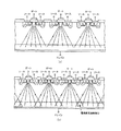
ところで、MOSFETの電気的特性のうち最も重要な特性の1つはオン抵抗である。MOSFETの動作原理上、キャリアはソースからドレインまでドリフトによって移動する。このためMOSFETのオン抵抗は図1に示すようにキャリアが移動する経路上の抵抗の総和で表される。すなわち、MOSFETのオン抵抗はソース抵抗Rs、チャンネル抵抗Rch、エピタキシャル層の抵抗Repi、基板抵抗Rsubの総和で表すことができる。MOSFETのオン抵抗を低減させる手法としては微細加工プロセスの適用が効果的である。微細加工プロセスによりセル寸法を縮小し高集積化を図ることにより単位体積当りの総チャンネル幅が広くなりチャンネル抵抗Rchが低減できる。しかも、総チャンネル幅が広くなれば電流経路の面積比率が増加するためエピ層抵抗Repiも低減する。このため、セルの高集積化はオン抵抗低減に極めて効果的である。図2は、セルの高集積化によるオン抵抗低減効果を示したものであり、図2(a)は微細化前、図2(b)は微細化後のキャリアの流れを示している。とりわけSiCを用いた半導体デバイスにおいては、オン抵抗の低減が重要な技術課題の1つとなっており、微細加工プロセスの適用が不可欠となる。
しかしながら、微細加工プロセスを適用して電流経路の面積比率を高めると、動作時において図2(b)に示すように、ドレイン領域1の近傍に電流密度過剰部分が形成され易くなる。このことは、通常のSi半導体よりもむしろSiC半導体において深刻な問題となる。ここで、図3に図1に示すA−A線に沿った断面の不純物の濃度分布を示す。SiC半導体においてはn型のドーパントとして窒素Nが用いられるのが一般的である。SiC中にドーパントとして窒素を導入すると、図3に示すように低濃度のドリフト層2と高濃度のn型基板層1との界面付近の濃度勾配は急峻となる。その結果、SiC基板を使用したMOSFETは従来のSi基板を使用したMOSFETと比較して、セルを高集積化したときに生じるドレイン近傍の電流密度過剰部分で電界集中や電流集中が起りやすく、大電流化、高耐圧化の妨げとなっていた。
However, when the area ratio of the current path is increased by applying the microfabrication process, an excessive current density portion is likely to be formed in the vicinity of the
本発明は、かかる点に鑑みてなされたものであり、縦型構造のパワーMOSFET、特にSiC基板を使用した縦型構造のパワーMOSFETにおいてセルの高集積化を図った場合でも電界集中および電流集中を回避して大電流化および高耐圧化を図ることができるMOSFETおよびその製造方法を提供することを目的とする。 The present invention has been made in view of the above points, and even in the case where a cell is highly integrated in a vertical structure power MOSFET, particularly in a vertical structure power MOSFET using a SiC substrate, electric field concentration and current concentration are achieved. It is an object of the present invention to provide a MOSFET and a method for manufacturing the same that can increase the current and the breakdown voltage by avoiding the above.
本発明の縦型MOSFETの製造方法は、第1の導電型を有する半導体からなる基板を用意するステップと、前記基板上に原料ガスおよび前記第1の導電型のドーパントガスを導入して気相反応によりバッファー層をエピタキシャル成長させるバッファー層形成ステップと、前記バッファー層上に原料ガスおよび前記第1の導電型のドーパントガスを導入して気相反応によりドリフト層をエピタキシャル成長させるドリフト層形成ステップと、前記ドリフト層表面に前記第2の導電型の不純物をイオン注入してボディ領域を形成するステップと、前記ボディ領域内に前記第1の導電型の不純物をイオン注入してソース領域を形成するステップと、を含み、前記バッファー層形成ステップにおいて、前記ドーパントガスの導入量を順次減少させ、前記ドリフト層形成ステップにおいては、前記ドーパントガスとして窒素を用い、前記基板が設置されたチャンバー内に前記原料ガスおよび前記ドーパントガスを導入し、前記ドーパントガスの導入量を前記チャンバー内の真空度により制御することを特徴としている。 Method for manufacturing the vertical MOSFET of the present invention, step a gas phase by introducing the raw material gas and the first conductivity type dopant gas to the substrate providing a substrate comprising a semiconductor material having a first conductivity type a buffer layer forming step of epitaxially growing a Riva Ffa layer by the reaction, drift epitaxially growing a Lido lift layer by the vapor phase reaction by introducing a material gas and said first conductivity type dopant gas to the buffer layer a layer forming step, forming a ball de region said second conductivity type impurity into the drift layer surface by ion implantation, the first conductivity type impurity is ion-implanted into the body region and forming a source over source region, a, in the buffer layer forming step, successively reducing the amount of introduction of the dopant gas In the drift layer forming step, nitrogen is used as the dopant gas, the source gas and the dopant gas are introduced into a chamber in which the substrate is installed, and the amount of the dopant gas introduced depends on the degree of vacuum in the chamber. It is characterized by control .
本発明のMOSFETによればセルの微細化に伴って動作時において電流密度過剰部分が生じることとなった場合でも、ドレイン領域近傍での電界集中および電流集中を緩和することができ、デバイスの大電流化および高耐圧化を図ることが可能となる。 According to the MOSFET of the present invention, electric field concentration and current concentration in the vicinity of the drain region can be alleviated even when an excessive current density portion occurs during operation due to cell miniaturization. It becomes possible to achieve current and high breakdown voltage.
(第1実施例)
以下、本発明の実施例について図面を参照しつつ説明する。以下に示す実施例においてはSiC基板を使用したMOSFETに本発明を適用した場合を例に説明するが、本発明は、通常のSi基板を使用したMOSFETにも適用可能である。図4は本発明の第1実施例に係るSiC基板を使用した縦型MOSFETの単位セルの断面構造図である。MOSFET100は、ドレインとして機能する不純物濃度1×1020cm−3のn型4H−SiC単結晶からなるn型SiC基板層10上に例えば不純物濃度5×1015cm−3のn型単結晶からなるn型ドリフト層12がバッファー層11を介して形成されている。バッファー層11は、その不純物濃度がSiC基板層10よりも低く、且つドリフト層12よりも高く設定されたn型SiC単結晶からなり、ドリフト層12からSiC基板層10に至る区間の不純物濃度勾配を緩和させる役割を担う層である。具体的には、バッファー層11は基板表面からの深さ位置に応じて互いに異なる濃度のドーパントがSiC中にドーピングされた3つの層11a、11b、11cからなり、SiC基板層10に隣接する最下層11aが最も不純物濃度が高く、ドリフト層12に隣接する最上層11cが最も不純物濃度が低く、これらの層の中間に形成された中間層11bは最上層11cと最下層11aの中間の不純物濃度で形成される。すなわち、バッファー層11は、深さ位置に応じて段階的に不純物濃度が変化する濃度分布となっている。ドリフト層12の表面には例えば濃度5×1015cm−3のp型SiC単結晶からなるp型ボディ領域13が形成される。p型ボディ領域13内部には例えば濃度5×1020cm−3のn型SiC単結晶からなるn型ソース領域14が形成される。n型ソース領域14の端部からp型ボディ領域13の端部に至る部分は反転層が形成されるチャンネル領域である。SiC基板表面にはチャンネル領域を覆うようにSiO2からなるゲート酸化膜15が形成され、ゲート酸化膜15上にはポリシリコンからなるゲート電極16が形成されている。n型SiC基板層10の裏面にはこれと電気的に接続されたドレイン電極17が形成され、n型ソース領域14上にはこれと電気的に接続されたソース電極18が形成されている。ゲート電極16は層間絶縁膜19により覆われており、ゲート電極16とソース電極18とは絶縁されている。
(First embodiment)
Embodiments of the present invention will be described below with reference to the drawings. In the following embodiments, a case where the present invention is applied to a MOSFET using a SiC substrate will be described as an example. However, the present invention can also be applied to a MOSFET using a normal Si substrate. FIG. 4 is a sectional structural view of a unit cell of a vertical MOSFET using the SiC substrate according to the first embodiment of the present invention. The
かかる構造のMOSFET100の動作原理は基本的には従来構造のものと同様である。すなわち、ゲート電極16にしきい値以上のゲート電圧が印加されることにより、p型ボディ領域13の表面に電子が誘起され反転層が形成される。これにより、n型ソース領域14とドリフト層12との間に電流経路が形成され、この状態においてドレイン電極17をソース電極18に対して正バイアスすると電子がn型ソース領域14からドレインとして機能するSiC基板層10に向かって流れることにより電流が流れる。
The operation principle of the
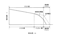
図5は、上記構造を有するMOSFET100の図4に示すB−B線に沿った断面における不純物濃度分布を示したものであり、横軸はMOSFET100の表面からの深さ方向の距離、縦軸は不純物濃度を示している。本発明のMOSFET100は上記したように高濃度のSiC基板層10とドリフト層12との間に不純物濃度が段階的に変化するように積層された複数の層からなるバッファー層11が設けられているために、ドリフト層12からSiC基板層10に至る区間の濃度勾配は、従来構造のものと比較して緩やかになっているのが理解できる。図6は、MOSFET100の動作時における図4中のB−B線断面に沿った電界強度分布を示したものである。図6には、比較として従来構造における図1中のA−A線断面に沿った電界強度分布が破線で示されている。図6に示すように本発明のMOSFET100においては、バッファー層11がドリフト層12とSiC基板層10との間に設けられ、このバッファー層11内で電界強度が低下するため動作時において電流密度が過剰となるSiC基板層10(ドレイン)近傍の電界強度が従来構造と比較して低下する。すなわち、バッファー層11の作用によりドリフト層12からSiC基板層10に至る区間の不純物濃度勾配が緩やかになることによって、セルの微細化に伴ってドレイン近傍で電流密度過剰部分が生じた場合でも、電界集中が起こりにくくなり、SiC基板を使用したMOSFETにおいて大電流化および高耐圧化を図ることが可能となる。
FIG. 5 shows the impurity concentration distribution in the cross section along the line BB shown in FIG. 4 of the
次に上記構造を有するMOSFET100の製造方法について図7を参照しつつ説明する。図7(a)から(g)は、MOSFET100の製造工程を各ステップ毎に示した断面図である。まず、例えば不純物濃度1×1020cm−3の窒素Nがドーピングされた厚さ300um程度のn型4H−SiC基板10を用意する。SiC基板10は例えば昇華法により製造される(図7(a))。
Next, a method for manufacturing
次に、SiC基板10上にバッファー層11およびドリフト層12を順次エピタキシャル成長させる。エピタキシャル成長は、例えばCVD(chemical Vapor Deposition 化学気相成長)法を用いて行うことができる。原料ガスはSi源にSiH4、C源にC3H8を用い、n型ドーパントガスとしてN2を用いる。キャリアガスH2により原料ガスおよびドーパントガスを反応管内に導入し、サセプタ上で加熱されたSiC基板10上にバッファー層11およびドリフト層12を順次形成する。成長温度は例えば1500℃とし、反応管内の圧力は例えば40Torrとする。バッファー層11は上記したように互いに不純物濃度の異なる3つの層11a、11b、11cにより構成されるが、CVD成膜工程においてはn型ドーパントガスであるN2の流量を順次変化させることにより、任意且つ高精度に不純物濃度を制御可能である。すなわち、バッファー層11のうち最も不純物濃度の高い最下層11aを形成する際にはN2流量を多くし、最も不純物濃度の低い最上層11cを形成する際にはN2流量を少なくする。中間層11bを形成する際にはその中間の流量とする。このように、CVD成膜工程においてドーパントガスの流量を段階的に変化させることにより、不純物濃度が段階的に変化する複数の層からなるバッファー層11を形成することが可能となる(図7(b))。ドリフト層12は、バッファー層11の形成後、引き続きCVD成膜工程において形成される。ドリフト層12の不純物濃度もバッファー層11と同様にドーパントガスの流量を調整することにより制御され、バッファー層11上にドリフト層12を成長させる(図7(c))。
Next, the
次にエピタキシャル成長させたドリフト層12の表面にフォトマスク20を形成し、p型不物イオン注入を行いp型ボディ領域13を形成する。フォトマスク20は、CVD法により堆積した厚さ1um程度のSiO2膜をフォトリソグラフィーによりパターン加工して形成する。イオン種は例えばアルミニウムAlを使用することができ、イオン注入は例えば注入エネルギー200KeV、ドーズ量5×1014cm−2で行う(図7(d))。尚、p型不純物としてはアルミニウムAlの代わりにホウ素Bを用いることとしてもよい。
Next, a
次に、基板表面にフォトマスク21を形成し、先の工程で形成したp型ボディ領域13内にn型不純物イオン注入を行いn型ソース領域14を形成する。イオン種は例えば窒素Nを使用することができ、イオン注入は例えば注入エネルギー100KeV、ドーズ量1×1015cm−2で行う(図7(e))。尚、n型不純物としては窒素Nの代わりにリンPを注入することとしてもよい。また、SiC単結晶中にイオン注入する場合は、イオン注入時に形成される結晶欠陥の熱アニールによる回復がSiに比べて困難であるため、結晶欠陥の回復に有効なイオン注入時に基板を加熱するホットイオン注入を行うことが好ましい。その後、例えば1500℃のアルゴン雰囲気中で30分間の活性化アニールを行う。
Next, a
次に、イオン注入後の基板を1100℃のWetO2中で5時間程度熱酸化して、基板表面にSiO2からなるゲート酸化膜15を形成する。尚、ゲート酸化膜の形成は、上記ウェット酸化法に限らずドライ酸素O2を用いたドライ酸化法やドライO2とドライ水素H2のガスを炉心間入口で燃焼させて水蒸気を発生させるパイロジェニック法を用いて行うこととしてもよい。次にゲート酸化膜15上にCVD法によりポリシリコンを堆積させ、フォトリソグラフィーによりパターン加工を施してゲート電極16を形成する(図7(f))。
Next, the substrate after ion implantation is thermally oxidized in WetO 2 at 1100 ° C. for about 5 hours to form a
次に、CVD法により基板表面全体を覆うように層間絶縁膜19を堆積させ、n型ソース領域14に対応する部分にコンタクト開口を形成する。続いてスパッタ法によりAlを基板表面に堆積させパターニングを施すことによりソース電極を18を形成する。次に、SiC基板層10の裏面側表面に例えばチタンTi、ニッケルNi、金Auを順次スパッタ法により堆積させ、ドレイン電極17を形成する(図7(g))。
Next, an
以上の工程を経ることにより、MOSFET100が完成する。上記した実施例においてはバッファー層11をCVD成膜工程においてドーパントガス(N2)の流量を段階的に変化させることにより形成することとしたが、SiCのドーパントガスとして用いられる窒素N2は大気中に多く含まれることから、CVD成膜工程において、CVDチャンバー内の真空度を段階的に変化させることにより上記した本発明のMOSFETの構造を得ることができる。すなわち、チャンバー内の真空度によりドーパントガスの導入量を制御するのである。具体的には、バッファー層11のうち最も不純物濃度の高い最下層11aを形成する際には、真空度を低くすることにより処理雰囲気中のN2含有量を多くし、最も不純物濃度の低い最上層11cを形成する際には真空度を高くすることにより処理雰囲気中のN2含有量を少なくする。中間層11bを形成する際にはその中間の真空度とする。更に、バッファー層11はCVD法以外の方法によっても形成することも可能である。以下にバッファー層11の他の形成方法について説明する。
The
まず、例えば濃度5×1018cm−3の窒素Nがドーピングされた厚さ300um程度のn型4H−SiC基板10を用意する。次にSiC基板10上にドリフト層12をエピタキシャル成長させる。エピタキシャル成長は、CVD法で行われ、原料ガスはSi源にSiH4、C源にC3H8を用い、n型ドーパントガスとしてN2を用いる。キャリアガスH2により原料ガスおよびn型ドーパントガスを反応管内に導入し、サセプタ上で加熱されたSiC基板10上に不純物濃度5×1015cm−3のドリフト層12を形成する。成長温度は例えば1500℃とし、反応管内の圧力は例えば40Torrとする。
First, for example, an n-type 4H—
ドリフト層12を形成した後、窒素Nの多重イオン注入によりドリフト層12とSiC基板10の界面付近に互いに不純物濃度の異なる複数の層からなるバッファー層11を形成する。すなわち、バッファー層11を構成する各層毎に注入エネルギーおよびドーズ量を変えてイオン注入を行うことにより所望の濃度分布を得る。具体的には、バッファー層11を構成する層のうちSiC基板層10に隣接する最下層11aを形成する際には、例えば注入エネルギー1200KeV、ドーズ量5×1014cm−2でイオン注入を行う。中間層11bを形成する際には、注入エネルギー1000KeV、ドーズ量5×1013cm−2でイオン注入を行う。そして、ドリフト層12に隣接する最上層11cを形成する際には注入エネルギー800KeV、ドーズ量5×1012cm−2でイオン注入を行う。尚、注入するイオン種は窒素N以外にリンPを用いることとしてもよい。図8に多重イオン注入により形成されたバッファー層11を含むMOSFET100の図4に示すB−B線に沿った断面における不純物濃度分布を示す。本製法においてはバッファー層11を構成する各層毎に注入エネルギーを順次変化させて濃度ピークが現れる深さ位置を制御し、各層毎にドーズ量を変化させることにより各層における不純物濃度を制御することで図8に示す如き不純物濃度分布を得ることができる。その結果、SiC基板層10とドリフト層12の界面近傍にこれらの層の不純物濃度勾配を緩和する役割を担うバッファー層11が形成されることになる。これ以降の製造工程は上記したものと同様であるのでその説明は省略する。
After the
(第2実施例)
図9に本発明の第2実施例に係るSiC基板を使用した縦型MOSFET200の単位セルの断面構造図を示す。第2実施例に係るMOSFET200の基本構造は、第1実施例のものと同様であるがバッファー層の構造が若干異なる。すなわち、第1実施例のMOSFET100に設けられたバッファー層11は、不純物濃度が段階的に変化するように積層された複数の層により構成されていた。これに対し本実施例に係るMOSFET200に設けられたバッファー層11´の構造は、深さ位置に応じて不純物濃度が連続的に変化する単一の層によって構成されている。図10は、図9に示すMOSFET200のC−C線に沿った断面における不純物濃度分布を示したものである。バッファー層11´は、基板表面からの深さ位置が増すにつれて不純物濃度が単調に増加するような濃度分布を有する。また、ドリフト層12との界面付近における不純物濃度はドリフト層12の不純物濃度と一致し、SiC基板層10との界面付近の不純物濃度はSiC基板層10の不純物濃度と一致している。このように、バッファー層11´の不純物濃度を連続的に変化させることによっても第1実施例と同様の効果を得ることができる。すなわち、バッファー層11´がドリフト層12とSiC基板層10との間に設けられることにより、動作時において電流密度が過剰となるSiC基板層10(ドレイン)近傍の電界強度が従来構造と比較して低下するという効果が得られる。これにより、セルの微細化に伴ってドレイン近傍で電流密度過剰部分が生じた場合でも、電界集中が起こりにくくなり、SiC基板を使用したMOSFETにおいて大電流化および高耐圧化を図ることが可能となる。
(Second embodiment)
FIG. 9 is a sectional structural view of a unit cell of a vertical MOSFET 200 using an SiC substrate according to a second embodiment of the present invention. The basic structure of the MOSFET 200 according to the second embodiment is the same as that of the first embodiment, but the structure of the buffer layer is slightly different. That is, the
上記の如き不純物濃度が深さに応じて連続的に変化するバッファー層11´を形成するためには、第1実施例と同様、CVD法を用いたエピタキシャル成長により形成することが可能である。すなわち、図10に示す如きバッファー層11´の濃度分布は、CVD成膜工程において原料ガスとともに導入するドーパントガスN2の流量を連続的に変化させることにより得ることが可能である。具体的には、CVD成膜工程においてバッファー層11´が下層部分から上層部分に向けて順次形成されていくのに伴ってドーパントガスN2の流量が連続変化するように徐々に減じていくことにより、本実施例に係るバッファー層11´の構造を得ることが可能である。ドリフト層12は、バッファー層11´の形成後、引き続きCVD法によりドーパントガスの流量を一定とすることにより形成される。このように形成されたバッファー層11´を有するMOSFETにおいても第1実施例のものと同様の作用効果が得られる。尚、バッファー層11´を形成するための他の方法としては、CVDチャンバー内の真空度を連続的に変化させるにより形成することが可能である。具体的には、CVD成膜工程において、バッファー層11´が下層部分から上層部分に向けて順次形成されていくのに伴って、CVDチャンバー内の窒素含有量が連続変化するように徐々にチャンバー内の真空度を高めていくことにより本実施例のバッファー層11´の構造を得ることができる。
In order to form the buffer layer 11 'in which the impurity concentration changes continuously according to the depth as described above, it can be formed by epitaxial growth using the CVD method as in the first embodiment. That is, the concentration distribution of the
以上の説明から明らかなように、本発明のMOSFETによれば、SiC基板層とドリフト層の間にこれら各層の不純物濃度勾配を緩和する役割を担うバッファー層を設けることとしたので、セルの微細化に伴って動作時において電流密度過剰部分が生じることとなった場合でも、ドレイン近傍での電界集中および電流集中が緩和され、デバイスの大電流化および高耐圧化を図ることが可能となる。また、本発明に係るMOSFETの構造は、通常のSi基板を用いたMOSFETに適用する場合でも一定の効果を有するが、SiC基板層とドリフト層の界面近傍の不純物濃度が急峻に変化するといった特徴を有するSiC基板を使用したMOSFETに適用した場合に顕著な効果を奏する。尚、本発明を通常のSi基板を用いたMOSFETに適用する場合は、バッファー層をCVD法により形成する際に用いられるドーパントガスとして例えばホスフィン(PH3)等を用いることができる。 As is clear from the above description, according to the MOSFET of the present invention, since the buffer layer that plays a role of relaxing the impurity concentration gradient of each layer is provided between the SiC substrate layer and the drift layer, the fine structure of the cell Even if an excessive current density portion is generated during operation, the electric field concentration and current concentration in the vicinity of the drain are alleviated, and it is possible to increase the device current and increase the breakdown voltage. The MOSFET structure according to the present invention has a certain effect even when applied to a MOSFET using a normal Si substrate, but the impurity concentration in the vicinity of the interface between the SiC substrate layer and the drift layer changes sharply. When the present invention is applied to a MOSFET using a SiC substrate having the above, a remarkable effect is obtained. In the case of applying the present invention to MOSFET using conventional Si substrate, for example a phosphine buffer layer as a dopant gas used when forming by CVD (PH 3) or the like can be used.
尚、以上の説明においては、本発明をNチャンネルMOSFETに適用した場合を例に説明したが、ドーパントを変更することによりPチャンネルMOSFETにも適用できることはもちろんである。 In the above description, the case where the present invention is applied to an N-channel MOSFET has been described as an example, but it is needless to say that the present invention can also be applied to a P-channel MOSFET by changing the dopant.
10 SiC基板層
11 バッファー層
12 ドリフト層
13 p型ボディ領域
14 n型ソース領域
15 ゲート酸化膜
16 ゲート電極
17 ドレイン電極
18 ソース電極
DESCRIPTION OF
Claims (1)
第1の導電型を有する半導体からなる基板を用意するステップと、Providing a substrate made of a semiconductor having a first conductivity type;
前記基板上に原料ガスおよび前記第1の導電型のドーパントガスを導入して気相反応によりバッファー層をエピタキシャル成長させるバッファー層形成ステップと、A buffer layer forming step of introducing a source gas and a dopant gas of the first conductivity type onto the substrate and epitaxially growing the buffer layer by a gas phase reaction;
前記バッファー層上に原料ガスおよび前記第1の導電型のドーパントガスを導入して気相反応によりドリフト層をエピタキシャル成長させるドリフト層形成ステップと、A drift layer forming step of introducing a source gas and a dopant gas of the first conductivity type onto the buffer layer and epitaxially growing the drift layer by a gas phase reaction;
前記ドリフト層表面に第2の導電型の不純物をイオン注入してボディ領域を形成するステップと、Ion implantation of a second conductivity type impurity into the drift layer surface to form a body region;
前記ボディ領域内に前記第1の導電型の不純物をイオン注入してソース領域を形成するステップと、を含み、Forming a source region by ion-implanting the first conductivity type impurity into the body region;
前記バッファー層形成ステップにおいて、前記ドーパントガスの導入量を順次減少させ、In the buffer layer forming step, the introduction amount of the dopant gas is sequentially reduced,
前記ドリフト層形成ステップにおいては、前記ドーパントガスとして窒素を用い、前記基板が設置されたチャンバー内に前記原料ガスおよび前記ドーパントガスを導入し、前記ドーパントガスの導入量を前記チャンバー内の真空度により制御することを特徴とする縦型MOSFETの製造方法。In the drift layer forming step, nitrogen is used as the dopant gas, the source gas and the dopant gas are introduced into a chamber in which the substrate is installed, and the amount of the dopant gas introduced depends on the degree of vacuum in the chamber. A method of manufacturing a vertical MOSFET, wherein the vertical MOSFET is controlled.
Priority Applications (1)
| Application Number | Priority Date | Filing Date | Title |
|---|---|---|---|
| JP2007336781A JP5236281B2 (en) | 2007-12-27 | 2007-12-27 | Manufacturing method of vertical MOSFET |
Applications Claiming Priority (1)
| Application Number | Priority Date | Filing Date | Title |
|---|---|---|---|
| JP2007336781A JP5236281B2 (en) | 2007-12-27 | 2007-12-27 | Manufacturing method of vertical MOSFET |
Publications (2)
| Publication Number | Publication Date |
|---|---|
| JP2009158788A JP2009158788A (en) | 2009-07-16 |
| JP5236281B2 true JP5236281B2 (en) | 2013-07-17 |
Family
ID=40962468
Family Applications (1)
| Application Number | Title | Priority Date | Filing Date |
|---|---|---|---|
| JP2007336781A Active JP5236281B2 (en) | 2007-12-27 | 2007-12-27 | Manufacturing method of vertical MOSFET |
Country Status (1)
| Country | Link |
|---|---|
| JP (1) | JP5236281B2 (en) |
Cited By (1)
| Publication number | Priority date | Publication date | Assignee | Title |
|---|---|---|---|---|
| KR20170100629A (en) * | 2015-01-27 | 2017-09-04 | 미쓰비시덴키 가부시키가이샤 | Semiconductor device |
Families Citing this family (9)
| Publication number | Priority date | Publication date | Assignee | Title |
|---|---|---|---|---|
| JP5458509B2 (en) * | 2008-06-04 | 2014-04-02 | 日立金属株式会社 | Silicon carbide semiconductor substrate |
| CN102714143B (en) * | 2010-01-08 | 2016-01-20 | 三菱电机株式会社 | Epitaxial wafer and semiconductor element |
| JP2012253108A (en) | 2011-06-01 | 2012-12-20 | Sumitomo Electric Ind Ltd | Silicon carbide semiconductor device and method of manufacturing the same |
| JP5637086B2 (en) * | 2011-07-07 | 2014-12-10 | 三菱電機株式会社 | Epitaxial wafer and semiconductor device |
| EP2874188A4 (en) | 2013-02-13 | 2016-04-13 | Fuji Electric Co Ltd | Semiconductor device |
| JP2017139362A (en) * | 2016-02-04 | 2017-08-10 | 株式会社東芝 | Semiconductor device |
| US10615274B2 (en) * | 2017-12-21 | 2020-04-07 | Cree, Inc. | Vertical semiconductor device with improved ruggedness |
| US11489069B2 (en) | 2017-12-21 | 2022-11-01 | Wolfspeed, Inc. | Vertical semiconductor device with improved ruggedness |
| CN108305900B (en) * | 2017-12-29 | 2022-02-15 | 重庆中科渝芯电子有限公司 | Slowly-varying doping material sheet of power MOSFET and manufacturing method thereof |
Family Cites Families (5)
| Publication number | Priority date | Publication date | Assignee | Title |
|---|---|---|---|---|
| JPS57153469A (en) * | 1981-03-18 | 1982-09-22 | Toshiba Corp | Insulated gate type field effect transistor |
| JPH0734471B2 (en) * | 1987-09-24 | 1995-04-12 | 三菱電機株式会社 | Field effect semiconductor device |
| JP3428459B2 (en) * | 1998-09-01 | 2003-07-22 | 富士電機株式会社 | Silicon carbide n-channel MOS semiconductor device and method of manufacturing the same |
| JP2000243957A (en) * | 1999-02-24 | 2000-09-08 | Nec Corp | Semiconductor device and manufacture thereof |
| JP2000286415A (en) * | 1999-03-29 | 2000-10-13 | Sanyo Electric Co Ltd | Mosfet element and manufacture thereof |
-
2007
- 2007-12-27 JP JP2007336781A patent/JP5236281B2/en active Active
Cited By (4)
| Publication number | Priority date | Publication date | Assignee | Title |
|---|---|---|---|---|
| KR20170100629A (en) * | 2015-01-27 | 2017-09-04 | 미쓰비시덴키 가부시키가이샤 | Semiconductor device |
| KR101970087B1 (en) * | 2015-01-27 | 2019-04-17 | 미쓰비시덴키 가부시키가이샤 | Semiconductor device |
| US10290711B2 (en) | 2015-01-27 | 2019-05-14 | Mitsubishi Electric Corporation | Semiconductor device |
| US10665677B2 (en) | 2015-01-27 | 2020-05-26 | Mitsubishi Electric Corporation | Semiconductor device |
Also Published As
| Publication number | Publication date |
|---|---|
| JP2009158788A (en) | 2009-07-16 |
Similar Documents
| Publication | Publication Date | Title |
|---|---|---|
| JP5236281B2 (en) | Manufacturing method of vertical MOSFET | |
| US8697555B2 (en) | Method of producing semiconductor device and semiconductor device | |
| JP5603008B2 (en) | Method for forming SiCMOSFET having large inversion layer mobility | |
| CN101859706B (en) | Silicon carbide semiconductor device and manufacturing method thereof | |
| JP5433352B2 (en) | Manufacturing method of semiconductor device | |
| JP3811624B2 (en) | Semiconductor device | |
| JP5519901B2 (en) | Silicon carbide field effect transistor and method of manufacturing the same | |
| JP4965576B2 (en) | Semiconductor device and manufacturing method thereof | |
| KR102324000B1 (en) | Silicon carbide semiconductor device, and methods for manufacturing thereof | |
| JP7103444B2 (en) | Silicon carbide semiconductor device | |
| JP2006066439A (en) | Semiconductor device and its manufacturing method | |
| US6559068B2 (en) | Method for improving inversion layer mobility in a silicon carbide metal-oxide semiconductor field-effect transistor | |
| JP4857697B2 (en) | Silicon carbide semiconductor device | |
| JP2014222735A (en) | Semiconductor device and manufacturing method thereof | |
| JP4549167B2 (en) | Method for manufacturing silicon carbide semiconductor device | |
| JP4842527B2 (en) | Manufacturing method of semiconductor device | |
| JP2010034481A (en) | Method of manufacturing semiconductor device, and semiconductor device | |
| CN103681256B (en) | A kind of silicon carbide MOSFET device and preparation method thereof | |
| JP2009043880A (en) | Method of manufacturing silicon carbide semiconductor device and silicon carbide semiconductor device | |
| JP5197474B2 (en) | Method for manufacturing silicon carbide semiconductor device | |
| JP2014222734A (en) | Semiconductor device and manufacturing method thereof | |
| JP4857698B2 (en) | Silicon carbide semiconductor device | |
| CN105161526B (en) | The method for improving vertical conductive structure SiC MOSFET channel mobilities | |
| JP2004039946A (en) | Manufacturing method of semiconductor device | |
| WO2007004595A2 (en) | Semiconductor device and manufacturing method thereof |
Legal Events
| Date | Code | Title | Description |
|---|---|---|---|
| A621 | Written request for application examination |
Free format text: JAPANESE INTERMEDIATE CODE: A621 Effective date: 20101101 |
|
| A131 | Notification of reasons for refusal |
Free format text: JAPANESE INTERMEDIATE CODE: A131 Effective date: 20121225 |
|
| A977 | Report on retrieval |
Free format text: JAPANESE INTERMEDIATE CODE: A971007 Effective date: 20121227 |
|
| A521 | Written amendment |
Free format text: JAPANESE INTERMEDIATE CODE: A523 Effective date: 20130218 |
|
| TRDD | Decision of grant or rejection written | ||
| A01 | Written decision to grant a patent or to grant a registration (utility model) |
Free format text: JAPANESE INTERMEDIATE CODE: A01 Effective date: 20130312 |
|
| A61 | First payment of annual fees (during grant procedure) |
Free format text: JAPANESE INTERMEDIATE CODE: A61 Effective date: 20130327 |
|
| R150 | Certificate of patent or registration of utility model |
Free format text: JAPANESE INTERMEDIATE CODE: R150 Ref document number: 5236281 Country of ref document: JP Free format text: JAPANESE INTERMEDIATE CODE: R150 |
|
| FPAY | Renewal fee payment (event date is renewal date of database) |
Free format text: PAYMENT UNTIL: 20160405 Year of fee payment: 3 |