JP5232425B2 - 不揮発性半導体記憶装置およびその製造方法 - Google Patents
不揮発性半導体記憶装置およびその製造方法 Download PDFInfo
- Publication number
- JP5232425B2 JP5232425B2 JP2007233924A JP2007233924A JP5232425B2 JP 5232425 B2 JP5232425 B2 JP 5232425B2 JP 2007233924 A JP2007233924 A JP 2007233924A JP 2007233924 A JP2007233924 A JP 2007233924A JP 5232425 B2 JP5232425 B2 JP 5232425B2
- Authority
- JP
- Japan
- Prior art keywords
- film
- insulating film
- charge storage
- region
- memory device
- Prior art date
- Legal status (The legal status is an assumption and is not a legal conclusion. Google has not performed a legal analysis and makes no representation as to the accuracy of the status listed.)
- Expired - Fee Related
Links
Images


Classifications
-
- H—ELECTRICITY
- H01—ELECTRIC ELEMENTS
- H01L—SEMICONDUCTOR DEVICES NOT COVERED BY CLASS H10
- H01L21/00—Processes or apparatus adapted for the manufacture or treatment of semiconductor or solid state devices or of parts thereof
- H01L21/02—Manufacture or treatment of semiconductor devices or of parts thereof
- H01L21/04—Manufacture or treatment of semiconductor devices or of parts thereof the devices having potential barriers, e.g. a PN junction, depletion layer or carrier concentration layer
- H01L21/18—Manufacture or treatment of semiconductor devices or of parts thereof the devices having potential barriers, e.g. a PN junction, depletion layer or carrier concentration layer the devices having semiconductor bodies comprising elements of Group IV of the Periodic Table or AIIIBV compounds with or without impurities, e.g. doping materials
- H01L21/30—Treatment of semiconductor bodies using processes or apparatus not provided for in groups H01L21/20 - H01L21/26
- H01L21/31—Treatment of semiconductor bodies using processes or apparatus not provided for in groups H01L21/20 - H01L21/26 to form insulating layers thereon, e.g. for masking or by using photolithographic techniques; After treatment of these layers; Selection of materials for these layers
- H01L21/3105—After-treatment
- H01L21/31051—Planarisation of the insulating layers
-
- H—ELECTRICITY
- H10—SEMICONDUCTOR DEVICES; ELECTRIC SOLID-STATE DEVICES NOT OTHERWISE PROVIDED FOR
- H10D—INORGANIC ELECTRIC SEMICONDUCTOR DEVICES
- H10D30/00—Field-effect transistors [FET]
- H10D30/01—Manufacture or treatment
- H10D30/021—Manufacture or treatment of FETs having insulated gates [IGFET]
- H10D30/0411—Manufacture or treatment of FETs having insulated gates [IGFET] of FETs having floating gates
-
- H—ELECTRICITY
- H10—SEMICONDUCTOR DEVICES; ELECTRIC SOLID-STATE DEVICES NOT OTHERWISE PROVIDED FOR
- H10D—INORGANIC ELECTRIC SEMICONDUCTOR DEVICES
- H10D30/00—Field-effect transistors [FET]
- H10D30/60—Insulated-gate field-effect transistors [IGFET]
- H10D30/69—IGFETs having charge trapping gate insulators, e.g. MNOS transistors
- H10D30/694—IGFETs having charge trapping gate insulators, e.g. MNOS transistors characterised by the shapes, relative sizes or dispositions of the gate electrodes
-
- H—ELECTRICITY
- H10—SEMICONDUCTOR DEVICES; ELECTRIC SOLID-STATE DEVICES NOT OTHERWISE PROVIDED FOR
- H10D—INORGANIC ELECTRIC SEMICONDUCTOR DEVICES
- H10D64/00—Electrodes of devices having potential barriers
- H10D64/01—Manufacture or treatment
- H10D64/031—Manufacture or treatment of data-storage electrodes
- H10D64/035—Manufacture or treatment of data-storage electrodes comprising conductor-insulator-conductor-insulator-semiconductor structures
Landscapes
- Engineering & Computer Science (AREA)
- Physics & Mathematics (AREA)
- Condensed Matter Physics & Semiconductors (AREA)
- General Physics & Mathematics (AREA)
- Manufacturing & Machinery (AREA)
- Computer Hardware Design (AREA)
- Microelectronics & Electronic Packaging (AREA)
- Power Engineering (AREA)
- Non-Volatile Memory (AREA)
- Semiconductor Memories (AREA)
Description
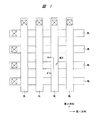
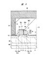
2 pウェル
3s ソース領域
3d ドレイン領域
4 電荷保持用絶縁膜
4a ボトム絶縁膜(第1絶縁膜)
4b 窒化領域
4c 電荷蓄積膜
4d 窒化領域
4e トップ絶縁膜(第2絶縁膜)
5 メモリゲート電極
6 側壁膜
7 層間絶縁膜
11 半導体基板
12ad,12as,12b 半導体領域
13 シリサイド層
14 ゲート絶縁膜
15 半導体領域
16 電荷保持用絶縁膜
16a ボトム絶縁膜
16c 電荷蓄積膜
16e トップ絶縁膜
17 半導体領域
18 層間絶縁膜
19 コンタクトホール
20 プラグ
BL ビット線
CG 選択ゲート電極
Drm ドレイン
M1 配線
MC1 メモリセル
MG メモリゲート電極
Srm ソース領域
WL ワード線
Claims (11)
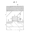
- 半導体基板と、前記半導体基板上に形成された第1絶縁膜と、前記第1絶縁膜上に形成された電荷蓄積膜と、前記電荷蓄積膜上に形成された第2絶縁膜と、前記第2絶縁膜上に形成されたゲート電極とを備えるメモリセルを有し、前記電荷蓄積膜が金属酸化膜により構成される不揮発性半導体記憶装置であって、
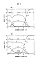
前記第1絶縁膜は一層の絶縁膜からなり、前記第1絶縁膜中の、前記半導体基板と前記第1絶縁膜との界面よりも前記第1絶縁膜と前記電荷蓄積膜との界面に近い領域に、窒素濃度が1原子%以上の窒化領域が形成されており、前記窒化領域の厚さが0.5nm以上、1.5nm以下であり、
前記電荷蓄積膜中の、前記第1絶縁膜と前記電荷蓄積膜との界面よりも前記電荷蓄積膜と前記第2絶縁膜との界面に近い領域に、窒素濃度が1原子%以上の窒化領域が形成されていることを特徴とする不揮発性半導体記憶装置。 - (a)半導体基板上に第1絶縁膜を形成する工程と、
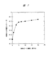
(b)前記第1絶縁膜に対してプラズマ窒化処理を行い、前記第1絶縁膜中の上面側に、ピーク値を有して窒素濃度が1原子%以上の窒化領域を形成する工程と、
(c)前記第1絶縁膜上に金属酸化膜からなる電荷蓄積膜を形成する工程と、
(d)前記電荷蓄積膜上に第2絶縁膜を形成する工程と、
(e)前記第2絶縁膜上にゲート電極を形成する工程とを含み、
前記窒化領域の厚さが0.5nm以上、1.5nm以下であることを特徴とする不揮発性半導体記憶装置の製造方法。 - 請求項2記載の不揮発性半導体記憶装置の製造方法において、前記(b)工程の前記プラズマ窒化処理の処理時間は30秒以上であることを特徴とする不揮発性半導体記憶装置の製造方法。
- 請求項2記載の不揮発性半導体記憶装置の製造方法において、前記第1絶縁膜中の前記窒素濃度のピーク値は5原子%以上、40原子%以下であることを特徴とする不揮発性半導体記憶装置の製造方法。
- 請求項2記載の不揮発性半導体記憶装置の製造方法において、前記窒素濃度のピーク値は前記第1絶縁膜と前記電荷蓄積膜との界面から2nm以内の領域に位置していることを特徴とする不揮発性半導体記憶装置の製造方法。
- 請求項2記載の不揮発性半導体記憶装置の製造方法において、前記電荷蓄積膜の物理的膜厚は20nm以下であることを特徴とする不揮発性半導体記憶装置の製造方法。
- 請求項2記載の不揮発性半導体記憶装置の製造方法において、前記電荷蓄積膜は、ALCVD法により形成されることを特徴とする不揮発性半導体記憶装置の製造方法。
- 請求項2記載の不揮発性半導体記憶装置の製造方法において、前記第1絶縁膜中の前記窒化領域は、前記半導体基板と前記第1絶縁膜との界面よりも前記第1絶縁膜と前記電荷蓄積膜との界面に近い領域に形成されることを特徴とする不揮発性半導体記憶装置の製造方法。
- 請求項2記載の不揮発性半導体記憶装置の製造方法において、前記(c)工程と前記(d)工程との間に、
(f)前記電荷蓄積膜に対してプラズマ窒化処理を行い、前記電荷蓄積膜中の上面側に、ピーク値を有して窒素濃度が1原子%以上の窒化領域を形成する工程、
をさらに含むことを特徴とする不揮発性半導体記憶装置の製造方法。 - 請求項9記載の不揮発性半導体記憶装置の製造方法において、前記電荷蓄積膜中の前記窒素濃度のピーク値は5原子%以上、40原子%以下であることを特徴とする不揮発性半導体記憶装置の製造方法。
- 請求項9記載の不揮発性半導体記憶装置の製造方法において、前記電荷蓄積膜中の前記窒化領域は、前記第1絶縁膜と前記電荷蓄積膜との界面よりも前記電荷蓄積膜と前記第2絶縁膜との界面に近い領域に形成されることを特徴とする不揮発性半導体記憶装置の製造方法。
Priority Applications (6)
| Application Number | Priority Date | Filing Date | Title |
|---|---|---|---|
| JP2007233924A JP5232425B2 (ja) | 2007-09-10 | 2007-09-10 | 不揮発性半導体記憶装置およびその製造方法 |
| KR1020080072232A KR100988092B1 (ko) | 2007-09-10 | 2008-07-24 | 불휘발성 반도체 기억 장치 및 그 제조 방법 |
| US12/186,488 US7719051B2 (en) | 2007-09-10 | 2008-08-05 | Nonvolatile semiconductor storage device and manufacturing method thereof |
| TW097130058A TWI390711B (zh) | 2007-09-10 | 2008-08-07 | 非揮發性半導體記憶裝置及其製造方法 |
| CN2008101449351A CN101388416B (zh) | 2007-09-10 | 2008-08-07 | 非易失性半导体存储装置及其制造方法 |
| US12/695,271 US7863134B2 (en) | 2007-09-10 | 2010-01-28 | Nonvolatile semiconductor storage device and manufacturing method thereof |
Applications Claiming Priority (1)
| Application Number | Priority Date | Filing Date | Title |
|---|---|---|---|
| JP2007233924A JP5232425B2 (ja) | 2007-09-10 | 2007-09-10 | 不揮発性半導体記憶装置およびその製造方法 |
Publications (2)
| Publication Number | Publication Date |
|---|---|
| JP2009065094A JP2009065094A (ja) | 2009-03-26 |
| JP5232425B2 true JP5232425B2 (ja) | 2013-07-10 |
Family
ID=40430913
Family Applications (1)
| Application Number | Title | Priority Date | Filing Date |
|---|---|---|---|
| JP2007233924A Expired - Fee Related JP5232425B2 (ja) | 2007-09-10 | 2007-09-10 | 不揮発性半導体記憶装置およびその製造方法 |
Country Status (5)
| Country | Link |
|---|---|
| US (2) | US7719051B2 (ja) |
| JP (1) | JP5232425B2 (ja) |
| KR (1) | KR100988092B1 (ja) |
| CN (1) | CN101388416B (ja) |
| TW (1) | TWI390711B (ja) |
Families Citing this family (5)
| Publication number | Priority date | Publication date | Assignee | Title |
|---|---|---|---|---|
| US20100059808A1 (en) * | 2008-09-10 | 2010-03-11 | Wei Zheng | Nonvolatile memories with charge trapping dielectric modified at the edges |
| CA2758205C (en) | 2009-04-09 | 2018-05-22 | Charles Skillman | Polymer having unsaturated cycloaliphatic functionality and coating compositions formed therefrom |
| US20120001179A1 (en) * | 2010-07-02 | 2012-01-05 | Semiconductor Energy Laboratory Co., Ltd. | Semiconductor device |
| JP2014053568A (ja) * | 2012-09-10 | 2014-03-20 | Toshiba Corp | 強誘電体メモリ及びその製造方法 |
| US10872898B2 (en) * | 2017-07-19 | 2020-12-22 | Cypress Semiconductor Corporation | Embedded non-volatile memory device and fabrication method of the same |
Family Cites Families (12)
| Publication number | Priority date | Publication date | Assignee | Title |
|---|---|---|---|---|
| JP3875455B2 (ja) * | 1999-04-28 | 2007-01-31 | 株式会社東芝 | 半導体装置の製造方法 |
| US6790755B2 (en) * | 2001-12-27 | 2004-09-14 | Advanced Micro Devices, Inc. | Preparation of stack high-K gate dielectrics with nitrided layer |
| JP2004158810A (ja) | 2002-09-10 | 2004-06-03 | Fujitsu Ltd | 不揮発性半導体メモリ |
| JP4358503B2 (ja) * | 2002-12-12 | 2009-11-04 | 忠弘 大見 | 不揮発性半導体記憶装置の製造方法 |
| US7405125B2 (en) * | 2004-06-01 | 2008-07-29 | Macronix International Co., Ltd. | Tunnel oxynitride in flash memories |
| KR100597642B1 (ko) * | 2004-07-30 | 2006-07-05 | 삼성전자주식회사 | 비휘발성 메모리 소자 및 그 제조방법 |
| JP4579637B2 (ja) * | 2004-10-01 | 2010-11-10 | 東京エレクトロン株式会社 | 半導体記憶装置及びその製造方法 |
| JP2006186245A (ja) * | 2004-12-28 | 2006-07-13 | Tokyo Electron Ltd | トンネル酸化膜の窒化処理方法、不揮発性メモリ素子の製造方法および不揮発性メモリ素子、ならびにコンピュータプログラムおよび記録媒体 |
| JP2006253311A (ja) * | 2005-03-09 | 2006-09-21 | Toshiba Corp | 半導体装置及びその製造方法 |
| JP4907173B2 (ja) * | 2006-01-05 | 2012-03-28 | マクロニクス インターナショナル カンパニー リミテッド | 不揮発性メモリセル、これを有するメモリアレイ、並びに、セル及びアレイの操作方法 |
| JP5032145B2 (ja) * | 2006-04-14 | 2012-09-26 | 株式会社東芝 | 半導体装置 |
| US7642616B2 (en) * | 2007-05-17 | 2010-01-05 | Micron Technology, Inc. | Tunnel and gate oxide comprising nitrogen for use with a semiconductor device and a process for forming the device |
-
2007
- 2007-09-10 JP JP2007233924A patent/JP5232425B2/ja not_active Expired - Fee Related
-
2008
- 2008-07-24 KR KR1020080072232A patent/KR100988092B1/ko not_active Expired - Fee Related
- 2008-08-05 US US12/186,488 patent/US7719051B2/en not_active Expired - Fee Related
- 2008-08-07 TW TW097130058A patent/TWI390711B/zh not_active IP Right Cessation
- 2008-08-07 CN CN2008101449351A patent/CN101388416B/zh not_active Expired - Fee Related
-
2010
- 2010-01-28 US US12/695,271 patent/US7863134B2/en active Active
Also Published As
| Publication number | Publication date |
|---|---|
| US7863134B2 (en) | 2011-01-04 |
| CN101388416A (zh) | 2009-03-18 |
| US7719051B2 (en) | 2010-05-18 |
| TW200924172A (en) | 2009-06-01 |
| TWI390711B (zh) | 2013-03-21 |
| US20100129998A1 (en) | 2010-05-27 |
| KR100988092B1 (ko) | 2010-10-18 |
| JP2009065094A (ja) | 2009-03-26 |
| US20090065848A1 (en) | 2009-03-12 |
| CN101388416B (zh) | 2011-07-13 |
| KR20090026720A (ko) | 2009-03-13 |
Similar Documents
| Publication | Publication Date | Title |
|---|---|---|
| US9117849B2 (en) | Nonvolatile semiconductor device and method of manufacturing the same | |
| US7872298B2 (en) | Split-gate type memory device | |
| TW561513B (en) | Semiconductor device and method of manufacturing the same | |
| JP5007017B2 (ja) | 半導体装置の製造方法 | |
| US10483114B2 (en) | Method of manufacturing semiconductor device having a nonvolatile memory and a MISFET | |
| EP3002780B1 (en) | Method of manufacturing semiconductor device | |
| JP2010183022A (ja) | 半導体装置およびその製造方法 | |
| US20110001179A1 (en) | Semiconductor device and manufacturing method of the same | |
| JP2009054707A (ja) | 半導体記憶装置およびその製造方法 | |
| JP2004356562A (ja) | 半導体装置の製造方法および半導体装置 | |
| CN104637947A (zh) | 半导体器件及其制造方法 | |
| US10446569B2 (en) | Semiconductor device and manufacturing method thereof | |
| JP4792620B2 (ja) | 不揮発性半導体記憶装置およびその製造方法 | |
| JP5232425B2 (ja) | 不揮発性半導体記憶装置およびその製造方法 | |
| WO1999065083A1 (en) | Semiconductor integrated circuit device and method of its manufacture | |
| US20230268400A1 (en) | Method of manufacturing semiconductor device | |
| CN100511682C (zh) | 半导体器件 |
Legal Events
| Date | Code | Title | Description |
|---|---|---|---|
| A621 | Written request for application examination |
Free format text: JAPANESE INTERMEDIATE CODE: A621 Effective date: 20100305 |
|
| A711 | Notification of change in applicant |
Free format text: JAPANESE INTERMEDIATE CODE: A712 Effective date: 20100528 |
|
| A131 | Notification of reasons for refusal |
Free format text: JAPANESE INTERMEDIATE CODE: A131 Effective date: 20120814 |
|
| A977 | Report on retrieval |
Free format text: JAPANESE INTERMEDIATE CODE: A971007 Effective date: 20120816 |
|
| A521 | Request for written amendment filed |
Free format text: JAPANESE INTERMEDIATE CODE: A523 Effective date: 20121015 |
|
| A131 | Notification of reasons for refusal |
Free format text: JAPANESE INTERMEDIATE CODE: A131 Effective date: 20121106 |
|
| A521 | Request for written amendment filed |
Free format text: JAPANESE INTERMEDIATE CODE: A523 Effective date: 20121228 |
|
| TRDD | Decision of grant or rejection written | ||
| A01 | Written decision to grant a patent or to grant a registration (utility model) |
Free format text: JAPANESE INTERMEDIATE CODE: A01 Effective date: 20130226 |
|
| A61 | First payment of annual fees (during grant procedure) |
Free format text: JAPANESE INTERMEDIATE CODE: A61 Effective date: 20130325 |
|
| FPAY | Renewal fee payment (event date is renewal date of database) |
Free format text: PAYMENT UNTIL: 20160329 Year of fee payment: 3 |
|
| R150 | Certificate of patent or registration of utility model |
Ref document number: 5232425 Country of ref document: JP Free format text: JAPANESE INTERMEDIATE CODE: R150 Free format text: JAPANESE INTERMEDIATE CODE: R150 |
|
| S531 | Written request for registration of change of domicile |
Free format text: JAPANESE INTERMEDIATE CODE: R313531 |
|
| R350 | Written notification of registration of transfer |
Free format text: JAPANESE INTERMEDIATE CODE: R350 |
|
| LAPS | Cancellation because of no payment of annual fees |