JP5225780B2 - 薄膜の製造方法および薄膜製造装置 - Google Patents
薄膜の製造方法および薄膜製造装置 Download PDFInfo
- Publication number
- JP5225780B2 JP5225780B2 JP2008203359A JP2008203359A JP5225780B2 JP 5225780 B2 JP5225780 B2 JP 5225780B2 JP 2008203359 A JP2008203359 A JP 2008203359A JP 2008203359 A JP2008203359 A JP 2008203359A JP 5225780 B2 JP5225780 B2 JP 5225780B2
- Authority
- JP
- Japan
- Prior art keywords
- substrate
- thin film
- target material
- emission intensity
- plume
- Prior art date
- Legal status (The legal status is an assumption and is not a legal conclusion. Google has not performed a legal analysis and makes no representation as to the accuracy of the status listed.)
- Expired - Fee Related
Links
- 239000010409 thin film Substances 0.000 title claims description 156
- 238000004519 manufacturing process Methods 0.000 title claims description 74
- 239000000758 substrate Substances 0.000 claims description 171
- 239000013077 target material Substances 0.000 claims description 132
- 238000005259 measurement Methods 0.000 claims description 24
- 238000003825 pressing Methods 0.000 claims description 22
- 230000001678 irradiating effect Effects 0.000 claims description 13
- 230000008859 change Effects 0.000 claims description 10
- 238000006243 chemical reaction Methods 0.000 claims description 9
- 239000002887 superconductor Substances 0.000 claims description 8
- 239000010408 film Substances 0.000 description 83
- 230000015572 biosynthetic process Effects 0.000 description 53
- 230000003028 elevating effect Effects 0.000 description 28
- 238000000034 method Methods 0.000 description 25
- 230000008569 process Effects 0.000 description 20
- 230000010355 oscillation Effects 0.000 description 12
- 238000001675 atomic spectrum Methods 0.000 description 7
- 238000010586 diagram Methods 0.000 description 7
- 230000000052 comparative effect Effects 0.000 description 6
- 239000000463 material Substances 0.000 description 6
- 239000002245 particle Substances 0.000 description 5
- 230000004048 modification Effects 0.000 description 4
- 238000012986 modification Methods 0.000 description 4
- 238000002360 preparation method Methods 0.000 description 4
- 238000002474 experimental method Methods 0.000 description 3
- 238000010438 heat treatment Methods 0.000 description 3
- 238000001228 spectrum Methods 0.000 description 3
- PXHVJJICTQNCMI-UHFFFAOYSA-N Nickel Chemical compound [Ni] PXHVJJICTQNCMI-UHFFFAOYSA-N 0.000 description 2
- 230000002093 peripheral effect Effects 0.000 description 2
- 230000007723 transport mechanism Effects 0.000 description 2
- 238000007740 vapor deposition Methods 0.000 description 2
- 241000954177 Bangana ariza Species 0.000 description 1
- MYMOFIZGZYHOMD-UHFFFAOYSA-N Dioxygen Chemical compound O=O MYMOFIZGZYHOMD-UHFFFAOYSA-N 0.000 description 1
- 229910052688 Gadolinium Inorganic materials 0.000 description 1
- 239000000956 alloy Substances 0.000 description 1
- 229910045601 alloy Inorganic materials 0.000 description 1
- 230000005540 biological transmission Effects 0.000 description 1
- 229910000420 cerium oxide Inorganic materials 0.000 description 1
- 229910001882 dioxygen Inorganic materials 0.000 description 1
- 230000000694 effects Effects 0.000 description 1
- 238000010894 electron beam technology Methods 0.000 description 1
- 239000007789 gas Substances 0.000 description 1
- 238000003384 imaging method Methods 0.000 description 1
- 230000006872 improvement Effects 0.000 description 1
- 230000007246 mechanism Effects 0.000 description 1
- 229910052759 nickel Inorganic materials 0.000 description 1
- 230000003647 oxidation Effects 0.000 description 1
- 238000007254 oxidation reaction Methods 0.000 description 1
- BMMGVYCKOGBVEV-UHFFFAOYSA-N oxo(oxoceriooxy)cerium Chemical compound [Ce]=O.O=[Ce]=O BMMGVYCKOGBVEV-UHFFFAOYSA-N 0.000 description 1
- 229910052761 rare earth metal Inorganic materials 0.000 description 1
- 238000009751 slip forming Methods 0.000 description 1
- 230000003595 spectral effect Effects 0.000 description 1
- 238000004544 sputter deposition Methods 0.000 description 1
- 238000012546 transfer Methods 0.000 description 1
Images


Landscapes
- Physical Vapour Deposition (AREA)
- Superconductors And Manufacturing Methods Therefor (AREA)
Description
本発明の効果を確認するために、本発明に従った方法および比較例の方法を用いて、レーザ蒸着法により帯状の基板の表面に超電導薄膜を形成する実験を行なった。
基板:
表面に超電導薄膜を形成するための基板として、長さが100m、幅が10mm、厚みが0.1mmであって、材質がニッケル系合金からなり表面に酸化セリウムの中間層を0.1μm形成した帯状の配向基板を2本(実施例の試料および比較例の試料の合計2本)準備した。
使用装置:
図6に示した構成の薄膜製造装置を用いた。
ターゲット材を構成する材料としてはHoBa2Cu3Oyを用いた。また、ターゲット材に照射するレーザ光の条件については、レーザ光の波長を248nm、出射エネルギーを1000mJ、繰返し周波数を150Hzとした。また、チャンバ中の雰囲気ガスを酸素ガス、雰囲気圧力を200mTorrとした。また、成膜温度(成膜時の基板の加熱温度)を750℃とした。
基本的に、上述した実施例の成膜条件と同様とした。ただし、ターゲット材と基板との間の距離は、成膜開始時に65mmに設定したあと、固定した。この結果、成膜開始時におけるプルームの輝度は4500cd/m2であったが、成膜処理の終了時には3600cd/m2となった。
実施例および比較例の試料について、それぞれ成膜開始時に薄膜が形成された領域と、成膜終了時に薄膜が形成された領域(すなわち帯状の基板の長手方向での両端部)において、試料を切出して超電導薄膜の膜厚および臨界電流値(Ic)を測定した。なお、切出した試料の長さは10cmとした。また、臨界電流値(Ic)の測定方法としては、四端子による通電法を用いた。
実施例:
実施例の試料において、成膜開始時に薄膜が形成された領域では超電導薄膜の厚みが0.20μm、臨界電流値Icが60Aであった。そして、成膜終了時に薄膜が形成された領域では、超電導薄膜の厚みが0.20μm、臨界電流値Icが58Aであった。
比較例の試料において、成膜開始時に薄膜が形成された領域では超電導薄膜の厚みが0.20μm、臨界電流値Icが60Aであった。そして、成膜終了時に薄膜が形成された領域では、超電導薄膜の厚みが0.16μm、臨界電流値Icが45Aであった。
Claims (4)
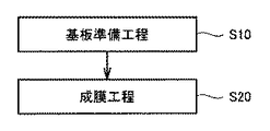
- 基板を準備する工程と、
前記基板と対向する位置にターゲット材を準備する工程と、
前記ターゲット材にエネルギー線を照射することにより、前記ターゲット材から放出される原子を含むプラズマを形成し、前記プラズマに含まれる前記原子を前記基板表面上に供給することにより薄膜を形成する工程とを備え、
前記薄膜を形成する工程では、前記基板に隣接する領域における前記プラズマの発光強度が、当該発光強度の初期値に対して±10%の範囲に入るように、前記基板と前記ターゲット材との間の距離が調整され、
前記薄膜を形成する工程において、前記プラズマの発光強度は前記プラズマの輝度であり、
前記基板を準備する工程では帯状の基板を準備し、
前記薄膜を形成する工程では、前記帯状の基板を移動させながら前記基板の表面上に前記薄膜が形成され、
前記薄膜を形成する工程では、前記帯状の基板の走行経路を規定するための押圧部材が前記基板に接触し、前記押圧部材が移動することにより前記基板と前記ターゲット材との間の距離が調整される、薄膜の製造方法。 - 前記薄膜を形成する工程では、超電導薄膜が形成される、請求項1に記載の薄膜の製造方法。
- 前記超電導薄膜はRE123系酸化物超電導体からなる、請求項2に記載の薄膜の製造方法。
- 反応室と、
前記反応室の内部に配置されたターゲット材支持部材と、
前記反応室の内部において、前記ターゲット材支持部材に対向するように帯状の基板を支持する基板支持部材と、
前記ターゲット材支持部材に支持されるターゲット材に照射するエネルギー線を発生させるエネルギー線源と、
前記エネルギー線が前記ターゲット材に照射されているとき、前記ターゲット材と前記基板との間の距離を変更する変更部材と、
前記ターゲット材に前記エネルギー線を照射することにより形成される、前記ターゲット材から放出される原子を含むプラズマの発光強度を測定する測定部材と、
前記測定部材により測定された前記プラズマの発光強度のデータに基づいて、前記変更部材を制御する制御部材とを備え、
前記変更部材は、前記ターゲット材支持部材の位置を変更する部材を含み、
前記基板支持部材は、前記ターゲット材の表面に沿った方向に前記基板を移動させる搬送部材と、前記移動される前記基板の走行経路を規定するために前記基板に接触する押圧部材とを含み、
前記変更部材は、前記押圧部材の位置を変更する部材を含む、薄膜製造装置。
Priority Applications (1)
| Application Number | Priority Date | Filing Date | Title |
|---|---|---|---|
| JP2008203359A JP5225780B2 (ja) | 2008-08-06 | 2008-08-06 | 薄膜の製造方法および薄膜製造装置 |
Applications Claiming Priority (1)
| Application Number | Priority Date | Filing Date | Title |
|---|---|---|---|
| JP2008203359A JP5225780B2 (ja) | 2008-08-06 | 2008-08-06 | 薄膜の製造方法および薄膜製造装置 |
Publications (2)
| Publication Number | Publication Date |
|---|---|
| JP2010037615A JP2010037615A (ja) | 2010-02-18 |
| JP5225780B2 true JP5225780B2 (ja) | 2013-07-03 |
Family
ID=42010464
Family Applications (1)
| Application Number | Title | Priority Date | Filing Date |
|---|---|---|---|
| JP2008203359A Expired - Fee Related JP5225780B2 (ja) | 2008-08-06 | 2008-08-06 | 薄膜の製造方法および薄膜製造装置 |
Country Status (1)
| Country | Link |
|---|---|
| JP (1) | JP5225780B2 (ja) |
Families Citing this family (1)
| Publication number | Priority date | Publication date | Assignee | Title |
|---|---|---|---|---|
| JP7174996B2 (ja) * | 2018-11-02 | 2022-11-18 | 国立大学法人東海国立大学機構 | パルスレーザーを用いた成膜方法及び成膜装置 |
Family Cites Families (4)
| Publication number | Priority date | Publication date | Assignee | Title |
|---|---|---|---|---|
| JPH03291371A (ja) * | 1989-12-27 | 1991-12-20 | Sumitomo Electric Ind Ltd | 薄膜製造方法 |
| JP2895683B2 (ja) * | 1992-07-30 | 1999-05-24 | 住友電気工業株式会社 | 酸化物超電導膜製造装置 |
| JPH08144051A (ja) * | 1994-11-21 | 1996-06-04 | Matsushita Electric Ind Co Ltd | レーザ・アブレーションを用いた薄膜形成法およびレーザ・アブレーション装置 |
| JP2007100620A (ja) * | 2005-10-05 | 2007-04-19 | Daihatsu Motor Co Ltd | 排ガス含有物質除去観測装置 |
-
2008
- 2008-08-06 JP JP2008203359A patent/JP5225780B2/ja not_active Expired - Fee Related
Also Published As
| Publication number | Publication date |
|---|---|
| JP2010037615A (ja) | 2010-02-18 |
Similar Documents
| Publication | Publication Date | Title |
|---|---|---|
| Bechelany et al. | Synthesis mechanisms of organized gold nanoparticles: influence of annealing temperature and atmosphere | |
| US6033741A (en) | Thin film forming apparatus using laser | |
| US5838016A (en) | Infrared radiation filament and method of manufacture | |
| KR101502390B1 (ko) | 그래핀의 제조 방법, 이를 포함하는 펄스레이저 공진기의 제조방법 및 이를 이용한 펄스레이저의 제조 방법 | |
| HUT61842A (en) | Method and equipment for spectroscopic analysing metal bath in the course of processing | |
| KR100403792B1 (ko) | 레이저표면처리장치및방법 | |
| JP5225780B2 (ja) | 薄膜の製造方法および薄膜製造装置 | |
| JP2003234288A (ja) | 多結晶半導体膜と半導体素子の製造方法及び製造装置 | |
| JPH01122905A (ja) | 酸化物層を基板上に形成する方法 | |
| JP2003163167A (ja) | 多結晶半導体膜、多結晶半導体膜製造方法及びそれを用いた薄膜半導体素子 | |
| US20250362225A1 (en) | Absorption spectrum-based chemical vapor deposition online in-situ characterization system and method | |
| JP2005214726A (ja) | 光強度分布検出方法、光強度分布検出装置、アニール装置及びアニール方法 | |
| US8841625B2 (en) | Method for the detection of the irradiance distribution in an extreme ultraviolet light source device and an extreme ultraviolet light source device | |
| CN108423709A (zh) | 一种基于双脉冲激光液相烧蚀合成纳米晶的装置的烧蚀方法 | |
| Biermann et al. | In-situ control of molecular beam epitaxial growth by spectral reflectivity analysis | |
| CN113253368A (zh) | 一种宽波段薄膜高吸收体、制备方法及装置 | |
| US20230311247A1 (en) | Laser machining method and laser machining system | |
| TWI480409B (zh) | 臨場監控之薄膜製程系統及其方法 | |
| US11328831B2 (en) | Method for treating a reflective optical element for the EUV wavelength range, method for producing same, and treating apparatus | |
| JP2006185933A (ja) | レーザアニール方法およびレーザアニール装置 | |
| JP4880548B2 (ja) | シリコン半導体薄膜の結晶性評価装置及び方法 | |
| JP3733022B2 (ja) | シリコン薄膜の結晶性評価方法および評価装置ならびにレーザアニール法および装置 | |
| Lecoeur et al. | Growth of Er: Y2O3 thin films by pulsed laser ablation from metallic targets | |
| JP4545902B2 (ja) | 成膜方法 | |
| WO2010024447A2 (ja) | カラーセンター含有酸化マグネシウムとその薄膜、波長可変レーザー媒体、レーザー装置、光源デバイス |
Legal Events
| Date | Code | Title | Description |
|---|---|---|---|
| A621 | Written request for application examination |
Free format text: JAPANESE INTERMEDIATE CODE: A621 Effective date: 20110328 |
|
| A977 | Report on retrieval |
Free format text: JAPANESE INTERMEDIATE CODE: A971007 Effective date: 20120813 |
|
| A131 | Notification of reasons for refusal |
Free format text: JAPANESE INTERMEDIATE CODE: A131 Effective date: 20120828 |
|
| A521 | Written amendment |
Free format text: JAPANESE INTERMEDIATE CODE: A523 Effective date: 20121024 |
|
| TRDD | Decision of grant or rejection written | ||
| A01 | Written decision to grant a patent or to grant a registration (utility model) |
Free format text: JAPANESE INTERMEDIATE CODE: A01 Effective date: 20130305 |
|
| A61 | First payment of annual fees (during grant procedure) |
Free format text: JAPANESE INTERMEDIATE CODE: A61 Effective date: 20130313 |
|
| R150 | Certificate of patent or registration of utility model |
Free format text: JAPANESE INTERMEDIATE CODE: R150 |
|
| FPAY | Renewal fee payment (event date is renewal date of database) |
Free format text: PAYMENT UNTIL: 20160322 Year of fee payment: 3 |
|
| S531 | Written request for registration of change of domicile |
Free format text: JAPANESE INTERMEDIATE CODE: R313531 |
|
| R350 | Written notification of registration of transfer |
Free format text: JAPANESE INTERMEDIATE CODE: R350 |
|
| LAPS | Cancellation because of no payment of annual fees |