JP5225780B2 - Thin film manufacturing method and thin film manufacturing apparatus - Google Patents
Thin film manufacturing method and thin film manufacturing apparatus Download PDFInfo
- Publication number
- JP5225780B2 JP5225780B2 JP2008203359A JP2008203359A JP5225780B2 JP 5225780 B2 JP5225780 B2 JP 5225780B2 JP 2008203359 A JP2008203359 A JP 2008203359A JP 2008203359 A JP2008203359 A JP 2008203359A JP 5225780 B2 JP5225780 B2 JP 5225780B2
- Authority
- JP
- Japan
- Prior art keywords
- substrate
- thin film
- target material
- emission intensity
- plume
- Prior art date
- Legal status (The legal status is an assumption and is not a legal conclusion. Google has not performed a legal analysis and makes no representation as to the accuracy of the status listed.)
- Expired - Fee Related
Links
- 239000010409 thin film Substances 0.000 title claims description 156
- 238000004519 manufacturing process Methods 0.000 title claims description 74
- 239000000758 substrate Substances 0.000 claims description 171
- 239000013077 target material Substances 0.000 claims description 132
- 238000005259 measurement Methods 0.000 claims description 24
- 238000003825 pressing Methods 0.000 claims description 22
- 230000001678 irradiating effect Effects 0.000 claims description 13
- 230000008859 change Effects 0.000 claims description 10
- 238000006243 chemical reaction Methods 0.000 claims description 9
- 239000002887 superconductor Substances 0.000 claims description 8
- 239000010408 film Substances 0.000 description 83
- 230000015572 biosynthetic process Effects 0.000 description 53
- 230000003028 elevating effect Effects 0.000 description 28
- 238000000034 method Methods 0.000 description 25
- 230000008569 process Effects 0.000 description 20
- 230000010355 oscillation Effects 0.000 description 12
- 238000001675 atomic spectrum Methods 0.000 description 7
- 238000010586 diagram Methods 0.000 description 7
- 230000000052 comparative effect Effects 0.000 description 6
- 239000000463 material Substances 0.000 description 6
- 239000002245 particle Substances 0.000 description 5
- 230000004048 modification Effects 0.000 description 4
- 238000012986 modification Methods 0.000 description 4
- 238000002360 preparation method Methods 0.000 description 4
- 238000002474 experimental method Methods 0.000 description 3
- 238000010438 heat treatment Methods 0.000 description 3
- 238000001228 spectrum Methods 0.000 description 3
- PXHVJJICTQNCMI-UHFFFAOYSA-N Nickel Chemical compound [Ni] PXHVJJICTQNCMI-UHFFFAOYSA-N 0.000 description 2
- 230000002093 peripheral effect Effects 0.000 description 2
- 230000007723 transport mechanism Effects 0.000 description 2
- 238000007740 vapor deposition Methods 0.000 description 2
- 241000954177 Bangana ariza Species 0.000 description 1
- MYMOFIZGZYHOMD-UHFFFAOYSA-N Dioxygen Chemical compound O=O MYMOFIZGZYHOMD-UHFFFAOYSA-N 0.000 description 1
- 229910052688 Gadolinium Inorganic materials 0.000 description 1
- 239000000956 alloy Substances 0.000 description 1
- 229910045601 alloy Inorganic materials 0.000 description 1
- 230000005540 biological transmission Effects 0.000 description 1
- 229910000420 cerium oxide Inorganic materials 0.000 description 1
- 229910001882 dioxygen Inorganic materials 0.000 description 1
- 230000000694 effects Effects 0.000 description 1
- 238000010894 electron beam technology Methods 0.000 description 1
- 239000007789 gas Substances 0.000 description 1
- 238000003384 imaging method Methods 0.000 description 1
- 230000006872 improvement Effects 0.000 description 1
- 230000007246 mechanism Effects 0.000 description 1
- 229910052759 nickel Inorganic materials 0.000 description 1
- 230000003647 oxidation Effects 0.000 description 1
- 238000007254 oxidation reaction Methods 0.000 description 1
- BMMGVYCKOGBVEV-UHFFFAOYSA-N oxo(oxoceriooxy)cerium Chemical compound [Ce]=O.O=[Ce]=O BMMGVYCKOGBVEV-UHFFFAOYSA-N 0.000 description 1
- 229910052761 rare earth metal Inorganic materials 0.000 description 1
- 238000009751 slip forming Methods 0.000 description 1
- 230000003595 spectral effect Effects 0.000 description 1
- 238000004544 sputter deposition Methods 0.000 description 1
- 238000012546 transfer Methods 0.000 description 1
Images


Landscapes
- Superconductors And Manufacturing Methods Therefor (AREA)
- Physical Vapour Deposition (AREA)
Description
この発明は、薄膜の製造方法および薄膜製造装置に関し、より特定的には、レーザを用いる薄膜の製造方法および薄膜製造装置に関する。 The present invention relates to a thin film manufacturing method and a thin film manufacturing apparatus, and more specifically to a thin film manufacturing method and a thin film manufacturing apparatus using a laser.
従来、レーザ蒸着法やレーザを用いたスパッタリング法などの薄膜の製造方法および薄膜製造装置が知られている。このような薄膜の製造方法では、薄膜の成膜処理を長時間続けると、反応室のレーザ入射窓にターゲット材から飛散した粒子が付着することにより、ターゲット材に入射するレーザ光のパワーが低下するという問題があった。このようにレーザ光のパワーが低下すると均質な薄膜を形成することができない。このような問題に対応するため、特許第2895683号明細書(以下、特許文献1と呼ぶ)では、レーザ入射窓の内側に回転式のレーザ透過性板材を配置し、粒子が直接レーザ入射窓に付着することを防止することが提案されている。
しかし、上述した従来の薄膜の製造方法および薄膜製造装置について発明者が詳細に検討したところ、形成する薄膜の均質性について更なる改善の余地があることが分かった。すなわち、上述のような従来の薄膜の製造方法および薄膜製造装置では、薄膜の形成を長時間続けると、ターゲット材においてレーザ光を照射された部分が凹形状となる。これは、レーザ光の照射によりターゲット材の表面が部分的に粒子として飛散することにより、当該表面が凹形状となるためである。このようにターゲット材の表面がレーザ光の照射により凹形状となると、ターゲット材においてレーザ光が照射される部分(凹形状となった部分)と、成膜対象物である基板との間の距離が大きくなり、結果的に基板表面での成膜条件が変化する。この結果、長時間成膜を続けた場合において、基板表面に形成される薄膜の均質性が低下することになっていた。 However, when the inventor examined the above-described conventional thin film manufacturing method and thin film manufacturing apparatus in detail, it was found that there was room for further improvement in the homogeneity of the thin film to be formed. That is, in the conventional thin film manufacturing method and thin film manufacturing apparatus as described above, when the thin film formation is continued for a long time, the portion of the target material irradiated with the laser light has a concave shape. This is because the surface of the target material is partially scattered as particles by the irradiation of the laser beam, so that the surface becomes concave. When the surface of the target material becomes concave due to laser light irradiation in this way, the distance between the portion of the target material irradiated with the laser light (the concave portion) and the substrate that is the film formation target As a result, film forming conditions on the substrate surface change. As a result, when film formation is continued for a long time, the homogeneity of the thin film formed on the substrate surface has been reduced.
また、上述した従来の薄膜製造装置のように、レーザ入射窓の内側に回転式のレーザ透過性板材を配置した場合であっても、成膜を長時間続けると当該レーザ透過性板材の表面に飛散した粒子が徐々に付着する。この結果、レーザ入射窓およびレーザ透過性板材を透過するレーザ光のパワーが低下し、やはり基板表面での成膜条件が変化する。この場合も、長時間成膜を続けた場合において、基板表面に形成される薄膜の均質性が低下することになっていた。 In addition, even when a rotary type laser transmissive plate is arranged inside the laser incident window as in the conventional thin film manufacturing apparatus described above, if the film formation is continued for a long time, the surface of the laser transmissive plate is applied. The scattered particles gradually adhere. As a result, the power of the laser beam transmitted through the laser incident window and the laser transmissive plate is lowered, and the film forming conditions on the substrate surface are also changed. Also in this case, when the film formation is continued for a long time, the homogeneity of the thin film formed on the surface of the substrate is lowered.
この発明は、上記のような課題を解決するために成されたものであり、この発明の目的は、均質な薄膜を長時間に渡って形成することが可能な薄膜の製造方法および薄膜製造装置を提供することである。 The present invention has been made to solve the above-described problems, and an object of the present invention is to provide a thin film manufacturing method and a thin film manufacturing apparatus capable of forming a homogeneous thin film over a long period of time. Is to provide.
この発明に従った薄膜の製造方法は、基板を準備する工程と、基板と対向する位置にターゲット材を準備する工程と、ターゲット材にエネルギー線を照射することにより、ターゲット材から放出される原子を含むプラズマを形成し、プラズマに含まれる原子を基板表面上に供給することにより薄膜を形成する工程とを備える。薄膜を形成する工程では、基板に隣接する領域におけるプラズマの発光強度が、当該発光強度の初期値に対して±10%の範囲に入るように、基板とターゲット材との間の距離が調整される。薄膜を形成する工程において、プラズマの発光強度はプラズマの輝度である。基板を準備する工程では帯状の基板を準備する。薄膜を形成する工程では、帯状の基板を移動させながら基板の表面上に薄膜が形成される。薄膜を形成する工程では、帯状の基板の走行経路を規定するための押圧部材が基板に接触し、押圧部材が移動することにより基板とターゲット材との間の距離が調整される。 The method of manufacturing a thin film according to the present invention includes a step of preparing a substrate, a step of preparing a target material at a position facing the substrate, and atoms emitted from the target material by irradiating the target material with energy rays. And forming a thin film by supplying atoms contained in the plasma onto the substrate surface. In the process of forming the thin film, the distance between the substrate and the target material is adjusted so that the plasma emission intensity in the region adjacent to the substrate falls within a range of ± 10% with respect to the initial value of the emission intensity. The In the process of forming a thin film, the emission intensity of plasma is the brightness of the plasma. In the step of preparing the substrate, a belt-like substrate is prepared. In the step of forming the thin film, the thin film is formed on the surface of the substrate while moving the belt-shaped substrate. In the step of forming the thin film, the pressing member for defining the travel path of the belt-shaped substrate comes into contact with the substrate, and the distance between the substrate and the target material is adjusted by moving the pressing member.
ここで、成膜を長時間続けた場合には、ターゲット材の表面がエネルギー線の照射により凹形状となったり、エネルギー線をターゲット材に照射するための透過窓に飛散した原子が付着したりすることによりターゲット材に照射されるエネルギー線のパワーが変化する。この場合、ターゲット材から放出される原子を含むプラズマ(プルーム)のサイズが小さくなり、結果的に成膜対象物である基板表面での成膜条件が変化する。そこで、本発明では上述のようにプラズマの状態を発光強度で検知し、当該発光強度に応じて基板とターゲット材との間の距離を調節する。たとえば、プルームが小さくなった場合には、基板とターゲット材との間の距離をより小さくすることで、基板表面近傍でのプルームの条件を成膜開始当初と同様に維持する、といった対応が考えられる。このようにすれば、成膜を長時間続けた場合であっても、基板表面での成膜条件を成膜開始時の条件に近似した条件に維持することができる。このため、均質な薄膜を長時間に渡って形成することができる。 Here, when film formation is continued for a long time, the surface of the target material becomes concave due to the irradiation of energy rays, or atoms scattered on the transmission window for irradiating the energy rays to the target material adhere By doing so, the power of the energy beam irradiated to the target material changes. In this case, the size of the plasma (plume) containing atoms emitted from the target material is reduced, and as a result, the film formation conditions on the substrate surface, which is the film formation target, change. Therefore, in the present invention, the plasma state is detected by the emission intensity as described above, and the distance between the substrate and the target material is adjusted according to the emission intensity. For example, if the plume becomes smaller, the distance between the substrate and the target material can be made smaller so that the plume conditions near the substrate surface can be maintained in the same way as at the beginning of film formation. It is done. In this way, even when the film formation is continued for a long time, the film formation conditions on the substrate surface can be maintained at conditions approximate to the conditions at the start of film formation. For this reason, a homogeneous thin film can be formed over a long time.
ここで、エネルギー線とは、たとえばレーザ光や電子線など、ターゲット材に照射されることにより当該ターゲット材の表面を構成する原子を飛散させてプラズマを形成することが可能な電磁波および粒子線を意味する。 Here, the energy beam is an electromagnetic wave or particle beam that can form plasma by irradiating the target material, such as a laser beam or an electron beam, to scatter atoms constituting the surface of the target material. means.
この発明に従った薄膜製造装置は、反応室と、ターゲット材支持部材と、基板支持部材と、エネルギー線源と、変更部材と、測定部材と、制御部材とを備える。ターゲット材支持部材は反応室の内部に配置される。基板支持部材は、反応室の内部において、ターゲット材支持部材に対向するように帯状の基板を支持する。エネルギー線源は、ターゲット材支持部材に支持されるターゲット材に照射するエネルギー線を発生させる。変更部材は、エネルギー線がターゲット材に照射されているとき、ターゲット材と基板との間の距離を変更する。測定部材は、ターゲット材にエネルギー線を照射することにより形成される、ターゲット材から放出される原子を含むプラズマの発光強度を測定する。制御部材は、測定部材により測定されたプラズマの発光強度のデータに基づいて、変更部材を制御する。変更部材は、ターゲット材支持部材の位置を変更する部材を含む。基板支持部材は、ターゲット材の表面に沿った方向に基板を移動させる搬送部材と、移動される基板の走行経路を規定するために基板に接触する押圧部材とを含む。変更部材は、押圧部材の位置を変更する部材を含む。 The thin film manufacturing apparatus according to the present invention includes a reaction chamber, a target material support member, a substrate support member, an energy ray source, a change member, a measurement member, and a control member . The target material support member is disposed inside the reaction chamber. The substrate support member supports the belt- like substrate so as to face the target material support member inside the reaction chamber. The energy beam source generates energy beams that irradiate the target material supported by the target material support member. The changing member changes the distance between the target material and the substrate when the energy beam is irradiated on the target material. The measurement member measures the emission intensity of plasma formed by irradiating the target material with energy rays and containing atoms emitted from the target material. The control member controls the changing member based on the plasma emission intensity data measured by the measuring member. The change member includes a member that changes the position of the target material support member. The substrate support member includes a transport member that moves the substrate in a direction along the surface of the target material, and a pressing member that contacts the substrate in order to define a travel path of the moved substrate. The changing member includes a member that changes the position of the pressing member.
このようにすれば、エネルギー線がターゲット材に照射されることにより、ターゲット材から飛散する原子を含むプラズマが形成され、当該プラズマから基板表面に当該原子が供給されることで薄膜が形成される。そして、薄膜形成時に、プラズマの状態(すなわち成膜条件)がほぼ一定になるようにターゲット材と基板との間の距離を変更できるので、長時間成膜処理を行なう場合でも、均質な薄膜を形成することができる。 In this way, the target material is irradiated with energy rays, thereby forming a plasma containing atoms scattered from the target material, and a thin film is formed by supplying the atoms from the plasma to the substrate surface. . Since the distance between the target material and the substrate can be changed so that the plasma state (that is, the film formation conditions) is substantially constant during the thin film formation, a uniform thin film can be formed even when performing a film formation process for a long time. Can be formed.
この発明によれば、均質な薄膜を長時間に渡って形成することができる。 According to this invention, a homogeneous thin film can be formed over a long period of time.
以下、図面に基づいて本発明の実施の形態を説明する。なお、以下の図面において同一または相当する部分には同一の参照番号を付しその説明は繰返さない。 Hereinafter, embodiments of the present invention will be described with reference to the drawings. In the following drawings, the same or corresponding parts are denoted by the same reference numerals, and description thereof will not be repeated.
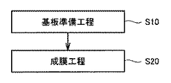
図1は、本発明に従った薄膜の製造方法を説明するためのフローチャートである。図2は、図1に示した成膜工程の内容を説明するためのフローチャートである。図3は、図1および図2に示した薄膜の製造方法を実施する薄膜製造装置を説明するための模式図である。図1〜図3を参照して、本発明に従った薄膜の製造方法および薄膜製造装置を説明する。 FIG. 1 is a flowchart for explaining a method of manufacturing a thin film according to the present invention. FIG. 2 is a flowchart for explaining the contents of the film forming process shown in FIG. FIG. 3 is a schematic diagram for explaining a thin film manufacturing apparatus for performing the thin film manufacturing method shown in FIGS. 1 and 2. The thin film manufacturing method and thin film manufacturing apparatus according to the present invention will be described with reference to FIGS.
図1および図2を参照して、本発明による薄膜の製造方法では、まず基板準備工程(S10)を実施する。具体的には、薄膜を表面に形成するべき基板を準備するとともに、後述する薄膜製造装置のチャンバ内に基板を配置する。この結果、ターゲット材と対向する位置に基板が配置されることになる。 Referring to FIGS. 1 and 2, in the thin film manufacturing method according to the present invention, first, a substrate preparation step (S10) is performed. Specifically, a substrate on which a thin film is to be formed is prepared, and the substrate is placed in a chamber of a thin film manufacturing apparatus described later. As a result, the substrate is disposed at a position facing the target material.
次に、成膜工程(S20)を実施する。具体的には、図2に示すような工程を実施する。ここで、成膜工程(S20)を説明するのに先立ち、図1および図2に示した薄膜の製造方法を実施する薄膜製造装置の構成を図3を参照しながら説明する。 Next, a film forming step (S20) is performed. Specifically, a process as shown in FIG. 2 is performed. Here, prior to the description of the film forming step (S20), the configuration of a thin film manufacturing apparatus that implements the thin film manufacturing method shown in FIGS. 1 and 2 will be described with reference to FIG.
図3に示すように、薄膜製造装置1は、反応室としてのチャンバ2と、ターゲット材支持部材としてのターゲット材用架台7と、基板支持部材としての基板用架台11と、エネルギー線源としてのレーザ発振部4と、変更部材としての昇降部材9、13および支柱8、12と、測定部材17と、制御部材としての制御部19および解析部18を備える。ターゲット材6を保持するターゲット材用架台7は、チャンバ2の内部に配置される。具体的には、ターゲット材用架台7の裏面側(ターゲット材6を保持する表面と反対側の裏面側)には支柱8の一方端部が接続固定されている。当該支柱8の他方端部は昇降部材9に接続される。昇降部材9はチャンバ2の底壁に固定されている。昇降部材9は支柱8を矢印21に示す方向に移動させることが可能になっている。このような昇降部材9の動作により、ターゲット材用架台7は矢印21に示す方向に移動可能になっている。なお、ターゲット材用架台7に保持されるターゲット材6としては、たとえば超電導体、より好ましくは酸化物超電導体、さらに好ましくはRE123系酸化物超電導体からなっている。ここで、RE123系酸化物超電導体とは、一般式REBa2Cu3Ox(REはたとえばY、Gd、Smなどの希土類元素の1種又は2種以上の元素を示す)で表される酸化物超電導体である。
As shown in FIG. 3, the thin film manufacturing apparatus 1 includes a
基板用架台11は、チャンバ2の内部において、ターゲット材用架台7に対向するように基板10を支持する。そのため、基板用架台11はターゲット材用架台7と対向する位置に配置される。また、基板用架台11の裏面側(基板10を保持する表面と反対側の裏面側)には支柱12の一方端部が接続されている。支柱12の他方端部は昇降部材13に接続される。昇降部材13はチャンバ2の上壁(底壁と対向する壁)に固定されている。昇降部材13は支柱12を矢印22に示す方向に移動させることが可能になっている。このような昇降部材13の動作により、基板用架台11は矢印22に示す方向に移動可能になっている。また、基板用架台11には、図示しないが基板10を加熱するためのヒータが設置されている。
The
レーザ発振部4は、ターゲット材用架台7に支持されるターゲット材6に照射するエネルギー線としてのレーザ光を発生させる。つまり、レーザ発振部4において発振したレーザ光は、矢印5に示すようにチャンバ2の壁に配置された窓部材3を透過してターゲット材6の表面に照射される。なお、窓部材3は、チャンバ2の側壁に形成された窓用凹部14(外側に凸形状となった凹部)の最外周部に形成された開口部を塞ぐように設置されている。窓部材3はレーザ光を透過可能な材料により構成される。
The laser oscillating unit 4 generates laser light as an energy beam applied to the
変更部材を構成する昇降部材9、13は、レーザ光がターゲット材6に照射されているとき、それぞれ支柱8、12を矢印21、22に示す方向に移動させることによりターゲット材6と基板10との間の距離を変更可能になっている。このため、薄膜形成時に、後述するようにプルーム20の状態(すなわち成膜条件)がほぼ一定になるようにターゲット材6と基板10との間の距離を変更できるので、長時間成膜処理を行なう場合でも、均質な薄膜を形成することができる。
The elevating
測定部材17は、チャンバ2の側壁に配置された窓部材16と対向する位置に配置されている。窓部材16は、チャンバ2の側壁に形成された窓用凹部15の最外周部における開口を塞ぐように配置されている。測定部材17は、レーザ光がターゲット材6に照射されることにより形成されるプラズマ(プルーム20)の先端部(基板10寄りの領域)を測定可能な位置に配置されている。測定部材17は、ターゲット材6にレーザ光を照射することにより形成される、ターゲット材6から放出される原子を含むプラズマの発光強度を測定する。測定部材17は解析部18に接続されている。なお、プラズマ(プルーム20)の発光強度として輝度を測定する場合には、測定部材17としては輝度計を用いることができる。
The measuring
解析部18では、測定部材17から出力される測定結果(プルーム20の発光強度を示す輝度などのデータ)を所定の基準値と対比し、その結果を制御部19に出力する。解析部18に接続された制御部19は、昇降部材9、13およびレーザ発振部4に接続されている。制御部19は、測定部材17により測定されたプルーム20の発光強度のデータに基づいて、昇降部材9、13の少なくともいずれか一方を制御する。また、制御部19は当該データに基づいてレーザ発振部4での出力を制御してもよい。
The
図1および図2に示した薄膜の製造方法において、図3に示した薄膜製造装置1のチャンバ2内に配置された基板10(基板用架台11に搭載された基板10)に対しては、図2に示すような工程により薄膜を形成する。以下、具体的に成膜工程(S20)を説明する。
In the thin film manufacturing method shown in FIGS. 1 and 2, for the substrate 10 (the
成膜工程(S20)では、図2に示すようにまずレーザ発振工程(S21)を実施する。この工程(S21)では、制御部19により制御信号がレーザ発振部4に入力されることにより、レーザ発振部4からレーザ光が発振される。発振されたレーザ光は、図3に示すように窓部材3を介してチャンバ2の内部に照射される。レーザ光は図3に示すようにチャンバ2内部のターゲット材6表面に入射する。
In the film forming step (S20), first, a laser oscillation step (S21) is performed as shown in FIG. In this step (S <b> 21), a laser beam is oscillated from the laser oscillation unit 4 when the
このようにレーザ光がターゲット材6の表面に照射されることにより、ターゲット材6の表面上(ターゲット材6と基板10との間の空間)にはプラズマ(プルーム20)が形成される。プルーム20は、ターゲット材6表面から放出された原子を含む。このプルーム20は図3に示すように基板10の近傍まで延びるように形成される。そして、プルーム20から放出される原子が基板10の表面(ターゲット材6と対向する表面)上に付着し、薄膜24が形成される。
By irradiating the surface of the
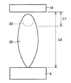
次に、プラズマ(プルーム20)の発光強度測定工程(S22)を実施する。具体的には、レーザ光を照射しながら(つまり基板10の表面に成膜処理を行ないながら)、測定部材17によりプルーム20の発光強度を測定する。ここで、発光強度としてはプルーム20の輝度を測定する。また、測定位置としては、図4に示すように基板10の膜が形成される表面近傍であることが好ましい。ここで、図4は、プルーム20の測定位置を説明するための模式図である。
Next, the light emission intensity measurement step (S22) of plasma (plume 20) is performed. Specifically, the emission intensity of the
図4に示すように、測定部材17(図3参照)によるプルーム20の測定対象領域23は、基板10の表面近傍の領域である。具体的には、測定対象領域23は基板10においてターゲット材6に対向する表面から5mmだけ離れた位置におけるプルーム20の中央点を中心として半径5mmの円形領域としてもよい。また、測定対象領域23を、基板10の表面から所定の距離L1内に配置してもよい。この場合、L1はたとえば基板10とターゲット材6との間の距離L0の1/3以下、より好ましくは1/4以下とする。また、測定対象領域23の位置は、プルーム20の全長の先端側(基板10側)であってプルーム20の全長の1/3の領域としてもよい。
As shown in FIG. 4, the
次に、図2に示すように発光強度が所定の範囲に入っているかどうかを判断する工程(S23)を実施する。この工程(S23)では、測定部材17により測定したプルーム20の発光強度(たとえば輝度)の値が、予め設定した基準値範囲に入っているかどうかを判断する。予め設定した基準範囲は、たとえば事前に実験などで決定しておいてもよいし、レーザ発振を開始してから所定時間(たとえば10秒)経過した後の発光強度の値を基準値として、当該基準値の±10%以内の範囲を基準範囲と設定してもよい。また、この工程(S23)は、図3に示した解析部18において実施してもよいが制御部19において実施してもよい。
Next, as shown in FIG. 2, a step (S23) of determining whether the emission intensity is within a predetermined range is performed. In this step (S23), it is determined whether the value of the emission intensity (for example, luminance) of the
上記工程(S23)において、YESと判断された場合には、成膜の終了条件が成立したかどうかを判断する工程(S25)へ進む。一方、工程(S23)においてNOと判断された(プルーム20の発光強度が基準範囲から外れた)場合には、位置調整工程(S24)が実施される。
If YES is determined in the step (S23), the process proceeds to a step (S25) in which it is determined whether or not a film formation end condition is satisfied. On the other hand, when it is determined NO in the step (S23) (the emission intensity of the
この位置調整工程(S24)では、具体的には制御部19からの制御信号により昇降部材9、13が制御され、ターゲット材用架台7および基板用架台11の位置が変更される。この結果、ターゲット材6と基板10との間の距離が変更される。たとえば、プルーム20の発光強度が基準範囲の下限を外れた場合には、ターゲット材6と基板10との間の距離をより短くするように昇降部材9、13が制御される。また、プルーム20の発光強度が基準範囲の上限を外れた場合には、ターゲット材6と基板10との間の距離をより長くするように昇降部材9、13が制御される。このとき、昇降部材9、13によりターゲット材用架台7および基板用架台11が移動される距離としては、予め1回当りの基準距離を決定しておいてもよい。
In this position adjusting step (S24), specifically, the elevating
また、ターゲット材6と基板10との間の距離を変更するため、昇降部材9、13のいずれか一方のみを動作させてもよい。このとき、動作させる昇降部材9、13のいずれか一方のみをチャンバ2内に配置し、他方の昇降部材はチャンバ内に配置しない構成としてもよい。
Further, in order to change the distance between the
このようにすれば、プルーム20の発光強度をほぼ一定に保つことができる。プルーム20の発光強度は、プルーム20の状態を反映しており、結果的に基板10表面での薄膜の成膜条件と相関がある。そのため、上記のような制御により基板10表面での成膜条件をほぼ一定に保つことができる。
In this way, the emission intensity of the
位置調整工程(S24)の次に(あるいは工程(S23)においてYESと判断された場合には)、上述した成膜の終了条件が成立したかどうかを判断する工程(S25)が実施される。具体的には、たとえば予め設定した成膜時間(レーザ発振を開始してからの経過時間)が経過したかどうかを判定する。なお、基板10の表面に形成される薄膜の膜厚をリアルタイムで測定し、当該膜厚が目的とした厚みに到達したかどうかを判断するようにしてもよい。この工程(S25)において、NOと判断されると、再び上記工程(S21)以下の工程を繰返す。一方、工程(S25)においてYESと判断された場合には、成膜工程が終了する。このようにして、基板10の表面に長時間に渡って成膜処理を行なう場合でも、成膜条件を安定させて均質な薄膜を形成することができる。
After the position adjustment step (S24) (or when it is determined YES in step (S23)), a step (S25) for determining whether or not the above-described film formation end conditions are satisfied is performed. Specifically, for example, it is determined whether or not a predetermined film formation time (elapsed time since the start of laser oscillation) has elapsed. Note that the film thickness of the thin film formed on the surface of the
なお、上述した工程では、プルーム20の発光強度として輝度を測定したが、輝度に代えてプルーム20の原子スペクトル強度を測定してもよい。ここで、原子スペクトル強度とは、プルーム20から放射される光をスペクトルに分光し、分光後の所定の波長(好ましくは成膜に関わる原子に起因する光の波長)の光の強度をいう。図5を参照して、より詳しく説明する。図5は、原子スペクトル強度を説明するための模式図である。
In the above-described process, the luminance is measured as the emission intensity of the
図5は、プルーム20から放射される光を分光して得られるスペクトルの一例を示す。図5では、横軸が光の波長を示し、縦軸が各波長の光の強度を示している。図5においては、ターゲット材6からプルーム20中に供給された原子に対応する波長の光を示すピーク25〜27が表わされている。そして、これらのピーク25〜27のうち、着目する原子に対応する波長の光のピーク(データ)の強度のデータを図2に示した工程(S22)で得るようにしてもよい。そして、上記強度の基準範囲を予め設定しておき、測定された強度が基準範囲に入っているかどうかを工程(S23)において判断してもよい。
FIG. 5 shows an example of a spectrum obtained by separating the light emitted from the
この場合、図3に示した薄膜製造装置1における測定部材17としては、たとえば分光光度計などを用いることができる。具体的には、プルーム20からの光をCCDカメラなどの撮像素子で取込み、当該光を分光器で波長スペクトルのデータとした上で、着目する原子に対応する波長の光の強度(ピークの高さ)を発光強度としてモニターしてもよい。
In this case, for example, a spectrophotometer or the like can be used as the
図6は、図3に示した本発明による薄膜製造装置の変形例を示す模式図である。図6を参照して、本発明による薄膜製造装置の変形例を説明する。 FIG. 6 is a schematic view showing a modification of the thin film manufacturing apparatus according to the present invention shown in FIG. A modification of the thin film manufacturing apparatus according to the present invention will be described with reference to FIG.
図6に示した薄膜製造装置1は、基本的には図3に示した薄膜製造装置1と同様の構成を備えるが、薄膜を形成する対象物である基板10として帯状の基板10を用いる点、および当該帯状の基板10を保持する部分の構成が図3に示した薄膜製造装置とは異なっている。具体的には、図6に示した薄膜製造装置1では、基板支持部材として、チャンバ2の内壁に回転可能に配置された、処理前の基板10を保持する払出リール31と、払出リール31から払出された帯状の基板10に薄膜が形成された後、当該薄膜付の基板10が巻取られる巻取リール32と、払出リール31から巻取リール32まで走行する基板10のうち、プルーム20と対向する部分(またはターゲット材6と対向する部分)の位置を矢印22に示す方向に移動させるための押圧部材35と、図示しない基板10加熱用のヒータとからなる搬送機構が設置されている。なお、押圧部材35において、基板10の裏面(ターゲット材6側の表面と反対側の面)側に接触する表面は、図6に示すように緩やかな曲面状になっていてもよいが、平坦な表面となっていてもよい。また、基板10との接触抵抗を低減するため、押圧部材35において基板10の裏面と接触する表面側には、たとえばガイドロールなどの回転部材を配置してもよい。
The thin film manufacturing apparatus 1 shown in FIG. 6 basically has the same configuration as the thin film manufacturing apparatus 1 shown in FIG. 3, but uses a strip-shaped
払出リール31および巻取リール32はいずれもチャンバ2に接続されている。押圧部材35は支柱12の一方端部と接続されている。そのため、昇降部材13が動作することにより、押圧部材35は矢印22に示した方向に移動可能となっている。
Both the
図6に示すように、払出リール31と巻取リール32とはプルーム20が形成される領域(ターゲット材6の正面に位置する領域)を挟むように配置される。払出リール31と巻取リール32との間には、基板10の走行経路を規定するための押圧部材35が配置されている。押圧部材35により案内される(つまり押圧部材35によりターゲット材6との間の距離が規定される)基板10の表面は、プルーム20と対向する(つまりターゲット材6においてレーザ光が照射される表面と対向する)。このため、押圧部材35により案内される部分において、基板10の表面には薄膜が形成される。なお、レーザ発振部4でのレーザ光の発振が開始されると同時に払出リール31および巻取リール32の回転が開始される。この結果、払出リール31および巻取リール32の間において表面に薄膜が形成された基板10が連続的に巻取リール32に巻取られる。このようにして、長尺の帯状である基板10の表面に薄膜を形成することができる。そして、このように長尺の基板10について薄膜を形成するために長時間の成膜処理を行なう場合には、本発明のようにプルーム20の発光強度に応じて基板10とターゲット材6との間の距離を調整することにより成膜条件をほぼ一定に保つことが、均質な薄膜の形成に特に効果的である。
As shown in FIG. 6, the pay-
上述した実施の形態と一部重複する部分もあるが、本発明の特徴的な構成を以下に列挙する。 Although there is a part which overlaps with embodiment mentioned above, the characteristic structure of this invention is enumerated below.
この発明に従った薄膜の製造方法は、図1および図2に示すように、基板を準備する工程(基板準備工程(S10))と、基板10と対向する位置にターゲット材6を準備する工程(基板準備工程(S10))と、ターゲット材6にエネルギー線としてのレーザ光を照射することにより、ターゲット材6から放出される原子を含むプラズマ(プルーム20)を形成し、プルーム20に含まれる原子を基板10表面上に供給することにより薄膜24を形成する工程(成膜工程(S20))とを備える。成膜工程(S20)では、プルーム20の発光強度に応じて基板10とターゲット材6との間の距離が調整される。
As shown in FIGS. 1 and 2, the thin film manufacturing method according to the present invention includes a step of preparing a substrate (substrate preparation step (S10)) and a step of preparing a
このようにすれば、プルーム20の状態を発光強度で検知し、当該発光強度に応じて基板10とターゲット材6との間の距離を調整するので、成膜を長時間続けた場合であっても、基板10表面での成膜条件を成膜開始時の条件に近似した条件に維持することができる。このため、均質な薄膜(膜厚や結晶性が均質な薄膜)を長時間に渡って形成することができる。
In this way, the state of the
上記薄膜の製造方法では、成膜工程(S20)において、プルーム20の発光強度はプルーム20の輝度(単位:cd/cm2)であってもよい。たとえば、当該プルーム20の輝度が薄膜製造開始時の輝度(たとえば薄膜製造開始後所定時間経過後(たとえば10秒後)のプルーム20の輝度)とほぼ同程度となるように、基板10とターゲット材6との間の距離を変更することができる。この場合、プルーム20の明るさを示す輝度を測定対象とするため、比較的簡単な測定装置でプルーム20の発光強度を測定することができる。この結果、薄膜製造装置1の装置構成を簡略化できるため、薄膜の製造コストの増大を抑制できる。
In the thin film manufacturing method, the emission intensity of the
上記薄膜の製造方法では、成膜工程(S20)において、プルーム20の発光強度は図5に示すようなプルーム20の原子スペクトル強度(特定の波長の光の強度)であってもよい。当該プルーム20の特定の原子スペクトル強度が薄膜製造開始時の強度(たとえば薄膜製造開始後所定時間経過後(たとえば10秒後)の原子スペクトル強度)とほぼ同程度となるように、基板10とターゲット材6との間の距離を変更することができる。この場合、プルーム20中に含まれる原子に応じて特定の波長の光が観測されるため、薄膜24の製造に関係する(薄膜24の材料となる)原子に対応する波長の光についての強度(図5のピークの高さに対応する原子スペクトル強度)を測定することで、薄膜の製造に直接関連するプルーム20の状態を検出することができる。このため、薄膜24の製造条件をより高い精度で調整することができる。この結果、形成される薄膜24について、成膜時間が長くなっても一定の膜質を確実に維持することができる。
In the thin film manufacturing method, in the film forming step (S20), the emission intensity of the
上記薄膜の製造方法において、成膜工程(S20)では、図4に示すように基板10に隣接する領域におけるプルーム20の発光強度に応じて基板10とターゲット材6との間の距離が調整されてもよい。この場合、基板10の表面に形成される薄膜の成膜条件に最も直接的に影響を及ぼすと考えられる、基板10に隣接する領域におけるプルーム20の発光強度を測定対象とすることで、成膜条件をより正確に反映したプルーム20の発光強度のデータを得ることができる。このため、成膜条件をより高い精度で調整することができる。この結果、形成される薄膜24について、成膜時間が長くなっても一定の膜質を確実に維持することができる。
In the thin film manufacturing method, in the film forming step (S20), the distance between the
上記薄膜の製造方法において、成膜工程(S20)では、図2に示した工程(S22)〜工程(S24)により、図4に示すように基板10に隣接する領域におけるプルーム20の発光強度が、発光強度の初期値に対して±10%の範囲に入るように、基板10とターゲット材6との間の距離が調整される。この場合、プルーム20の状態を初期状態(成膜を開始した時点から所定時間(たとえば10秒)経過したときのプルーム20の状態)とほぼ同等に維持することができる。この結果、成膜条件を長時間に渡ってほぼ一定に保つことができる。
In the thin film manufacturing method, in the film forming step (S20), the emission intensity of the
上記薄膜の製造方法において、成膜工程(S20)では、薄膜24として超電導薄膜が形成されてもよい。この場合、特性の均質な超電導薄膜を長時間に渡って形成することができる。また、上記薄膜の製造方法において、基板準備工程(S10)では図6に示すように帯状の基板10を準備してもよい。成膜工程(S20)では、図6で説明したように帯状の基板10を移動させながら基板10の表面上に超電導薄膜を形成してもよい。この場合、帯状の基板10の表面に、広い面積に渡って均質な超電導薄膜を形成することができる。このため、特性の優れた超電導薄膜線材を得ることができる。
In the thin film manufacturing method, a superconducting thin film may be formed as the
上記薄膜の製造方法において、超電導薄膜はRE123系酸化物超電導体からなっていてもよい。この場合、RE123系酸化物超電導体からなる均質な薄膜または当該薄膜を用いた超電導線材を形成することができる。 In the thin film manufacturing method, the superconducting thin film may be made of an RE123-based oxide superconductor. In this case, a homogeneous thin film made of RE123-based oxide superconductor or a superconducting wire using the thin film can be formed.
この発明に従った薄膜製造装置1は、反応室としてのチャンバ2と、ターゲット材支持部材としてのターゲット材用架台7と、基板支持部材としての基板用架台11(図3参照)または図6に示した押圧部材35を含む搬送機構と、エネルギー線源としてのレーザ発振部4と、変更部材としての昇降部材9、13および支柱8、12とを備える。ターゲット材用架台7はチャンバ2の内部に配置される。基板用架台11は、チャンバ2の内部において、ターゲット材用架台7に対向するように基板10を支持する。レーザ発振部4は、ターゲット材用架台7に支持されるターゲット材6に照射するエネルギー線としてのレーザ光を発生させる。昇降部材9、13および支柱8、12は、レーザ光がターゲット材6に照射されているとき(つまり成膜処理が行なわれているとき)、ターゲット材6と基板10との間の距離を変更する。
A thin film manufacturing apparatus 1 according to the present invention includes a
このようにすれば、レーザ光がターゲット材6に照射されることにより、ターゲット材6から飛散する原子を含むプルーム20が形成され、当該プルーム20から基板10表面に原子が供給されることで薄膜24が形成される。そして、薄膜24形成時に、プルーム20の状態(すなわち成膜条件)がほぼ一定になるようにターゲット材6と基板10との間の距離を変更できるので、長時間成膜処理を行なう場合でも、均質な薄膜24を形成することができる。
In this way, a
上記薄膜製造装置1は、ターゲット材6にレーザ光を照射することにより形成される、ターゲット材6から放出される原子を含むプルーム20の発光強度を測定する測定部材17を更に供えている。この場合、測定部材17によって測定されるプルーム20の発光強度に応じて、昇降部材9、13を制御することによりターゲット材6と基板10との間の距離を調整できる。この結果、プルーム20の状態(成膜条件)をほぼ一定に保つことができる。このため、長時間に渡って均質な薄膜24を形成することができる。
The thin film manufacturing apparatus 1 further includes a measuring
上記薄膜製造装置1は、測定部材17により測定されたプルーム20の発光強度のデータに基づいて、昇降部材9、13を制御する制御部19を更に備えている。この場合、制御部19を用いてプルーム20の発光強度のデータに応じて昇降部材9、13を制御できるので、プルーム20の状態(成膜条件)の調整を自動的に行なうことができる。
The thin film manufacturing apparatus 1 further includes a
上記薄膜製造装置1において、昇降部材9、13は、ターゲット材用架台7の位置を変更する昇降部材9を含む。この場合、たとえば基板10の位置を固定する装置構成であっても、ターゲット材6の位置を調整することによりターゲット材6と基板10との間の距離を変更できる。たとえば、図6に示すように基板支持部材として帯状の基板10をターゲット材6の表面に対してほぼ平行に走行させるような装置を用いる場合、当該装置全体を図6の矢印22に示す方向に移動させることは薄膜製造装置1の構成の複雑化に繋がる。このような場合には、基板支持部材としての押圧部材35などをチャンバ2に対して固定する(たとえばチャンバ2の上壁に直接押圧部材35を固定する)一方で、ターゲット材用架台7の位置を昇降部材9によって変更してもよい。このようにしてターゲット材6と基板10との間の距離を変更すれば、薄膜製造装置1の構成が過度に複雑化することを防止できる。
In the thin film manufacturing apparatus 1, the elevating
上記薄膜製造装置1において、昇降部材9、13は、基板用架台11の位置を変更する昇降部材13を含む。この場合、ターゲット材6の位置を固定する装置構成(たとえばターゲット材用架台7をチャンバ2の壁面に直接接続する構成)であっても、基板10の位置を調整することによりターゲット材6と基板10との間の距離を変更することができる。
In the thin film manufacturing apparatus 1, the elevating
上記薄膜製造装置1において、図6に示すように、押圧部材35を含む搬送機構は、ターゲット材6の表面に沿った方向に基板10を移動させる搬送部材としての払出リール31および巻取リール32を含んでいてもよい。この場合、基板10として長尺の帯状部材を用いることができる。すなわち、搬送部材(払出リール31、巻取リール32および押圧部材35)により帯状部材である基板10を、ターゲット材6の表面に沿った方向に移動させる(走行させる)ことにより、基板10の延在方向に沿って基板10全面に薄膜を形成することができる。そして、本発明による薄膜製造装置1では、長時間に渡って薄膜の製造条件をほぼ一定に保つことができるため、帯状部材である基板10の全長に渡って、均質な薄膜を形成することができる。
In the thin film manufacturing apparatus 1, as shown in FIG. 6, the transport mechanism including the pressing
(実施例)
本発明の効果を確認するために、本発明に従った方法および比較例の方法を用いて、レーザ蒸着法により帯状の基板の表面に超電導薄膜を形成する実験を行なった。
(Example)
In order to confirm the effect of the present invention, an experiment was conducted in which a superconducting thin film was formed on the surface of a belt-like substrate by laser vapor deposition using the method according to the present invention and the method of a comparative example.
(試料)
基板:
表面に超電導薄膜を形成するための基板として、長さが100m、幅が10mm、厚みが0.1mmであって、材質がニッケル系合金からなり表面に酸化セリウムの中間層を0.1μm形成した帯状の配向基板を2本(実施例の試料および比較例の試料の合計2本)準備した。
(sample)
substrate:
As a substrate for forming a superconducting thin film on the surface, the length was 100 m, the width was 10 mm, the thickness was 0.1 mm, and the material was made of a nickel-based alloy, and an intermediate layer of cerium oxide was formed on the surface by 0.1 μm. Two strip-like alignment substrates were prepared (two samples in total including the sample of the example and the sample of the comparative example).
(実験内容)
使用装置:
図6に示した構成の薄膜製造装置を用いた。
(Experiment contents)
Equipment used:
A thin film manufacturing apparatus having the configuration shown in FIG. 6 was used.
実施例の成膜条件:
ターゲット材を構成する材料としてはHoBa2Cu3Oyを用いた。また、ターゲット材に照射するレーザ光の条件については、レーザ光の波長を248nm、出射エネルギーを1000mJ、繰返し周波数を150Hzとした。また、チャンバ中の雰囲気ガスを酸素ガス、雰囲気圧力を200mTorrとした。また、成膜温度(成膜時の基板の加熱温度)を750℃とした。
Example film formation conditions:
HoBa 2 Cu 3 O y was used as a material constituting the target material. In addition, regarding the conditions of the laser beam irradiated to the target material, the wavelength of the laser beam was 248 nm, the emission energy was 1000 mJ, and the repetition frequency was 150 Hz. The atmospheric gas in the chamber was oxygen gas, and the atmospheric pressure was 200 mTorr. The film formation temperature (the heating temperature of the substrate during film formation) was 750 ° C.
また、基板の搬送速度を10m/hとした。このため、基板全長について成膜処理を行なうために要する時間は10時間となる。 The substrate transfer speed was 10 m / h. For this reason, the time required to perform the film forming process for the entire length of the substrate is 10 hours.
また、成膜開始時の基板とターゲット材との間の距離は65mmとした。さらに、測定部材として輝度計を用い、プルームの基板近傍領域(基板表面から5mmの位置を中心とした半径5mmの領域)の輝度を測定した。成膜開始時の当該輝度は4500cd/m2であった。その後、当該輝度の値が4500cd/m2の±10%以内になるように、ターゲット材を基板側に徐々に移動させた。具体的には、1時間毎に0.2mm、ターゲット材を基板側に近づけることにより、プルームの輝度が上述した数値範囲内となるようにした。この結果、成膜処理の終了時(成膜開始から10時間後)にはターゲット材と基板との間の距離は63mmとなった。 The distance between the substrate and the target material at the start of film formation was 65 mm. Further, a luminance meter was used as a measurement member, and the luminance of the plume substrate vicinity region (region having a radius of 5 mm centered on a position 5 mm from the substrate surface) was measured. The luminance at the start of film formation was 4500 cd / m 2 . Thereafter, the target material was gradually moved to the substrate side so that the luminance value was within ± 10% of 4500 cd / m 2 . Specifically, the luminance of the plume was within the numerical range described above by bringing the target material closer to the substrate side by 0.2 mm every hour. As a result, at the end of the film formation process (10 hours after the start of film formation), the distance between the target material and the substrate was 63 mm.
比較例の成膜条件:
基本的に、上述した実施例の成膜条件と同様とした。ただし、ターゲット材と基板との間の距離は、成膜開始時に65mmに設定したあと、固定した。この結果、成膜開始時におけるプルームの輝度は4500cd/m2であったが、成膜処理の終了時には3600cd/m2となった。
Film formation conditions for the comparative example:
Basically, the film forming conditions were the same as those in the above-described embodiment. However, the distance between the target material and the substrate was set to 65 mm at the start of film formation and then fixed. As a result, the brightness of the plume at the start film formation was the 4500 cd / m 2, at the end of the film forming process becomes 3600 cd / m 2.
(測定内容)
実施例および比較例の試料について、それぞれ成膜開始時に薄膜が形成された領域と、成膜終了時に薄膜が形成された領域(すなわち帯状の基板の長手方向での両端部)において、試料を切出して超電導薄膜の膜厚および臨界電流値(Ic)を測定した。なお、切出した試料の長さは10cmとした。また、臨界電流値(Ic)の測定方法としては、四端子による通電法を用いた。
(Measurement content)
For the samples of Examples and Comparative Examples, samples were cut out in a region where a thin film was formed at the start of film formation and a region where a thin film was formed at the end of film formation (that is, both ends in the longitudinal direction of the belt-like substrate). Then, the thickness and critical current value (Ic) of the superconducting thin film were measured. The length of the cut sample was 10 cm. Further, as a method for measuring the critical current value (Ic), an energization method using four terminals was used.
(測定結果)
実施例:
実施例の試料において、成膜開始時に薄膜が形成された領域では超電導薄膜の厚みが0.20μm、臨界電流値Icが60Aであった。そして、成膜終了時に薄膜が形成された領域では、超電導薄膜の厚みが0.20μm、臨界電流値Icが58Aであった。
(Measurement result)
Example:
In the sample of the example, the thickness of the superconducting thin film was 0.20 μm and the critical current value Ic was 60 A in the region where the thin film was formed at the start of film formation. In the region where the thin film was formed at the end of film formation, the thickness of the superconducting thin film was 0.20 μm and the critical current value Ic was 58A.
比較例:
比較例の試料において、成膜開始時に薄膜が形成された領域では超電導薄膜の厚みが0.20μm、臨界電流値Icが60Aであった。そして、成膜終了時に薄膜が形成された領域では、超電導薄膜の厚みが0.16μm、臨界電流値Icが45Aであった。
Comparative example:
In the sample of the comparative example, in the region where the thin film was formed at the start of film formation, the thickness of the superconducting thin film was 0.20 μm and the critical current value Ic was 60A. In the region where the thin film was formed at the end of film formation, the thickness of the superconducting thin film was 0.16 μm and the critical current value Ic was 45A.
上述した結果からもわかるように、本発明の実施例では、成膜処理を行なっている間、膜厚や膜質が安定した超電導薄膜を継続的に形成できている。 As can be seen from the results described above, in the example of the present invention, a superconducting thin film having a stable film thickness and film quality can be continuously formed during the film forming process.
今回開示された実施の形態および実施例はすべての点で例示であって制限的なものではないと考えられるべきである。本発明の範囲は上記した説明ではなくて特許請求の範囲によって示され、特許請求の範囲と均等の意味および範囲内でのすべての変更が含まれることが意図される。 It should be understood that the embodiments and examples disclosed herein are illustrative and non-restrictive in every respect. The scope of the present invention is defined by the terms of the claims, rather than the description above, and is intended to include any modifications within the scope and meaning equivalent to the terms of the claims.
この発明は、長尺の基板に薄膜を形成する場合や、大面積の基板に長時間をかけて薄膜を形成する場合などに、特に有利に適用される。 The present invention is particularly advantageously applied when a thin film is formed on a long substrate, or when a thin film is formed over a long area over a long time.
1 薄膜製造装置、2 チャンバ、3 窓部材、4 レーザ発振部、5,21,22 矢印、6 ターゲット材、7 ターゲット材用架台、8,12 支柱、9,13 昇降部材、10 基板、11 基板用架台、14,15 窓用凹部、16 窓部材、17 測定部材、18 解析部、19 制御部、20 プルーム、23 測定対象領域、24 薄膜、31 払出リール、32 巻取リール、35 押圧部材。 DESCRIPTION OF SYMBOLS 1 Thin film manufacturing apparatus, 2 chamber, 3 window member, 4 laser oscillation part, 5, 21, 22 arrow, 6 target material, 7 target material mount, 8, 12 support | pillar, 9,13 raising / lowering member, 10 board | substrate, 11 board | substrate Mounting base, 14, 15 Window recess, 16 Window member, 17 Measuring member, 18 Analysis unit, 19 Control unit, 20 Plume, 23 Measurement target area, 24 Thin film, 31 Dispensing reel, 32 Take-up reel, 35 Pressing member.
Claims (4)
前記基板と対向する位置にターゲット材を準備する工程と、
前記ターゲット材にエネルギー線を照射することにより、前記ターゲット材から放出される原子を含むプラズマを形成し、前記プラズマに含まれる前記原子を前記基板表面上に供給することにより薄膜を形成する工程とを備え、
前記薄膜を形成する工程では、前記基板に隣接する領域における前記プラズマの発光強度が、当該発光強度の初期値に対して±10%の範囲に入るように、前記基板と前記ターゲット材との間の距離が調整され、
前記薄膜を形成する工程において、前記プラズマの発光強度は前記プラズマの輝度であり、
前記基板を準備する工程では帯状の基板を準備し、
前記薄膜を形成する工程では、前記帯状の基板を移動させながら前記基板の表面上に前記薄膜が形成され、
前記薄膜を形成する工程では、前記帯状の基板の走行経路を規定するための押圧部材が前記基板に接触し、前記押圧部材が移動することにより前記基板と前記ターゲット材との間の距離が調整される、薄膜の製造方法。 Preparing a substrate;
Preparing a target material at a position facing the substrate;
Irradiating the target material with energy rays to form a plasma containing atoms emitted from the target material, and forming the thin film by supplying the atoms contained in the plasma onto the substrate surface; With
In the step of forming the thin film, the plasma emission intensity in a region adjacent to the substrate is between the substrate and the target material such that the plasma emission intensity falls within a range of ± 10% with respect to the initial value of the emission intensity. Is adjusted ,
In the step of forming the thin film, the emission intensity of the plasma is the brightness of the plasma,
In the step of preparing the substrate, a belt-shaped substrate is prepared,
In the step of forming the thin film, the thin film is formed on the surface of the substrate while moving the band-shaped substrate,
In the step of forming the thin film, a pressing member for defining a travel path of the belt-shaped substrate is in contact with the substrate, and the distance between the substrate and the target material is adjusted by the movement of the pressing member. is Ru, the method of manufacturing the thin film.
前記反応室の内部に配置されたターゲット材支持部材と、
前記反応室の内部において、前記ターゲット材支持部材に対向するように帯状の基板を支持する基板支持部材と、
前記ターゲット材支持部材に支持されるターゲット材に照射するエネルギー線を発生させるエネルギー線源と、
前記エネルギー線が前記ターゲット材に照射されているとき、前記ターゲット材と前記基板との間の距離を変更する変更部材と、
前記ターゲット材に前記エネルギー線を照射することにより形成される、前記ターゲット材から放出される原子を含むプラズマの発光強度を測定する測定部材と、
前記測定部材により測定された前記プラズマの発光強度のデータに基づいて、前記変更部材を制御する制御部材とを備え、
前記変更部材は、前記ターゲット材支持部材の位置を変更する部材を含み、
前記基板支持部材は、前記ターゲット材の表面に沿った方向に前記基板を移動させる搬送部材と、前記移動される前記基板の走行経路を規定するために前記基板に接触する押圧部材とを含み、
前記変更部材は、前記押圧部材の位置を変更する部材を含む、薄膜製造装置。 A reaction chamber;
A target material support member disposed inside the reaction chamber;
A substrate support member that supports a belt-shaped substrate so as to face the target material support member inside the reaction chamber;
An energy beam source for generating an energy beam for irradiating the target material supported by the target material support member;
A change member that changes a distance between the target material and the substrate when the energy beam is applied to the target material ;
A measurement member that measures the emission intensity of plasma that is formed by irradiating the target material with the energy beam and that includes atoms emitted from the target material;
A control member for controlling the change member based on data of the emission intensity of the plasma measured by the measurement member ;
The change member includes a member that changes the position of the target material support member,
The substrate support member includes a transport member that moves the substrate in a direction along the surface of the target material, and a pressing member that contacts the substrate to define a travel path of the moved substrate,
The said change member is a thin film manufacturing apparatus containing the member which changes the position of the said press member .
Priority Applications (1)
| Application Number | Priority Date | Filing Date | Title |
|---|---|---|---|
| JP2008203359A JP5225780B2 (en) | 2008-08-06 | 2008-08-06 | Thin film manufacturing method and thin film manufacturing apparatus |
Applications Claiming Priority (1)
| Application Number | Priority Date | Filing Date | Title |
|---|---|---|---|
| JP2008203359A JP5225780B2 (en) | 2008-08-06 | 2008-08-06 | Thin film manufacturing method and thin film manufacturing apparatus |
Publications (2)
| Publication Number | Publication Date |
|---|---|
| JP2010037615A JP2010037615A (en) | 2010-02-18 |
| JP5225780B2 true JP5225780B2 (en) | 2013-07-03 |
Family
ID=42010464
Family Applications (1)
| Application Number | Title | Priority Date | Filing Date |
|---|---|---|---|
| JP2008203359A Expired - Fee Related JP5225780B2 (en) | 2008-08-06 | 2008-08-06 | Thin film manufacturing method and thin film manufacturing apparatus |
Country Status (1)
| Country | Link |
|---|---|
| JP (1) | JP5225780B2 (en) |
Families Citing this family (1)
| Publication number | Priority date | Publication date | Assignee | Title |
|---|---|---|---|---|
| JP7174996B2 (en) * | 2018-11-02 | 2022-11-18 | 国立大学法人東海国立大学機構 | Film forming method and film forming apparatus using pulse laser |
Family Cites Families (4)
| Publication number | Priority date | Publication date | Assignee | Title |
|---|---|---|---|---|
| JPH03291371A (en) * | 1989-12-27 | 1991-12-20 | Sumitomo Electric Ind Ltd | Thin film formation |
| JP2895683B2 (en) * | 1992-07-30 | 1999-05-24 | 住友電気工業株式会社 | Oxide superconducting film production equipment |
| JPH08144051A (en) * | 1994-11-21 | 1996-06-04 | Matsushita Electric Ind Co Ltd | Thin film forming method using laser ablation and laser ablation apparatus |
| JP2007100620A (en) * | 2005-10-05 | 2007-04-19 | Daihatsu Motor Co Ltd | Exhaust gas content removal observation device |
-
2008
- 2008-08-06 JP JP2008203359A patent/JP5225780B2/en not_active Expired - Fee Related
Also Published As
| Publication number | Publication date |
|---|---|
| JP2010037615A (en) | 2010-02-18 |
Similar Documents
| Publication | Publication Date | Title |
|---|---|---|
| Bechelany et al. | Synthesis mechanisms of organized gold nanoparticles: influence of annealing temperature and atmosphere | |
| US6033741A (en) | Thin film forming apparatus using laser | |
| EP0842404B1 (en) | Infrared radiation filament and method of manufacture | |
| US8497987B2 (en) | Optical device unit and detection apparatus | |
| JP2000504498A (en) | Fabrication of electronic devices by energy beam crystallization | |
| KR100403792B1 (en) | Laser surface treatment apparatus and method | |
| JP5225780B2 (en) | Thin film manufacturing method and thin film manufacturing apparatus | |
| JP2020145366A (en) | Heat treatment method and heat treatment equipment | |
| JP2003234288A (en) | Method and apparatus for manufacturing polycrystalline semiconductor film and semiconductor element | |
| JPH01122905A (en) | Formation of oxide layer on substrate | |
| JP2003163167A (en) | Polycrystalline semiconductor film, method of manufacturing polycrystalline semiconductor film, and thin film semiconductor device using the same | |
| JP2005214726A (en) | Light-intensity distribution detection method, light-intensity distribution detecting device, annealing device, and annealing method | |
| CN108423709A (en) | A kind of ablative method of the device based on double-pulse laser liquid phase ablation synthesizing nanocrystalline | |
| EP2453218A1 (en) | A method for the detection of the irradiance distribution in an extreme ultraviolet light source device and a detection device for an extreme ultraviolet light source device | |
| CN113253368A (en) | Broadband thin film high absorber, preparation method and device | |
| Biermann et al. | In-situ control of molecular beam epitaxial growth by spectral reflectivity analysis | |
| JP6538389B2 (en) | Method of manufacturing diamond thin film, hot filament CVD apparatus and mechanical seal | |
| US20230311247A1 (en) | Laser machining method and laser machining system | |
| TWI480409B (en) | On-site monitoring film processing system and method thereof | |
| JP2006185933A (en) | Laser annealing method and annealer | |
| JP4880548B2 (en) | Apparatus and method for evaluating crystallinity of silicon semiconductor thin film | |
| EP3438744A1 (en) | Method for treating a reflective optical element for the euv wavelength range, method for producing same, and treating apparatus | |
| Lecoeur et al. | Growth of Er: Y2O3 thin films by pulsed laser ablation from metallic targets | |
| JP4545902B2 (en) | Deposition method | |
| WO2010024447A2 (en) | Color center-containing magnesium oxide and thin film of same, wavelength-variable laser medium, laser device, and light source device |
Legal Events
| Date | Code | Title | Description |
|---|---|---|---|
| A621 | Written request for application examination |
Free format text: JAPANESE INTERMEDIATE CODE: A621 Effective date: 20110328 |
|
| A977 | Report on retrieval |
Free format text: JAPANESE INTERMEDIATE CODE: A971007 Effective date: 20120813 |
|
| A131 | Notification of reasons for refusal |
Free format text: JAPANESE INTERMEDIATE CODE: A131 Effective date: 20120828 |
|
| A521 | Written amendment |
Free format text: JAPANESE INTERMEDIATE CODE: A523 Effective date: 20121024 |
|
| TRDD | Decision of grant or rejection written | ||
| A01 | Written decision to grant a patent or to grant a registration (utility model) |
Free format text: JAPANESE INTERMEDIATE CODE: A01 Effective date: 20130305 |
|
| A61 | First payment of annual fees (during grant procedure) |
Free format text: JAPANESE INTERMEDIATE CODE: A61 Effective date: 20130313 |
|
| R150 | Certificate of patent or registration of utility model |
Free format text: JAPANESE INTERMEDIATE CODE: R150 |
|
| FPAY | Renewal fee payment (event date is renewal date of database) |
Free format text: PAYMENT UNTIL: 20160322 Year of fee payment: 3 |
|
| S531 | Written request for registration of change of domicile |
Free format text: JAPANESE INTERMEDIATE CODE: R313531 |
|
| R350 | Written notification of registration of transfer |
Free format text: JAPANESE INTERMEDIATE CODE: R350 |
|
| LAPS | Cancellation because of no payment of annual fees |