JP5225526B2 - 液晶デバイス - Google Patents
液晶デバイス Download PDFInfo
- Publication number
- JP5225526B2 JP5225526B2 JP2001090213A JP2001090213A JP5225526B2 JP 5225526 B2 JP5225526 B2 JP 5225526B2 JP 2001090213 A JP2001090213 A JP 2001090213A JP 2001090213 A JP2001090213 A JP 2001090213A JP 5225526 B2 JP5225526 B2 JP 5225526B2
- Authority
- JP
- Japan
- Prior art keywords
- liquid crystal
- cell
- cell wall
- post
- random
- Prior art date
- Legal status (The legal status is an assumption and is not a legal conclusion. Google has not performed a legal analysis and makes no representation as to the accuracy of the status listed.)
- Expired - Fee Related
Links
Images


Classifications
-
- G—PHYSICS
- G02—OPTICS
- G02F—OPTICAL DEVICES OR ARRANGEMENTS FOR THE CONTROL OF LIGHT BY MODIFICATION OF THE OPTICAL PROPERTIES OF THE MEDIA OF THE ELEMENTS INVOLVED THEREIN; NON-LINEAR OPTICS; FREQUENCY-CHANGING OF LIGHT; OPTICAL LOGIC ELEMENTS; OPTICAL ANALOGUE/DIGITAL CONVERTERS
- G02F1/00—Devices or arrangements for the control of the intensity, colour, phase, polarisation or direction of light arriving from an independent light source, e.g. switching, gating or modulating; Non-linear optics
- G02F1/01—Devices or arrangements for the control of the intensity, colour, phase, polarisation or direction of light arriving from an independent light source, e.g. switching, gating or modulating; Non-linear optics for the control of the intensity, phase, polarisation or colour
- G02F1/13—Devices or arrangements for the control of the intensity, colour, phase, polarisation or direction of light arriving from an independent light source, e.g. switching, gating or modulating; Non-linear optics for the control of the intensity, phase, polarisation or colour based on liquid crystals, e.g. single liquid crystal display cells
- G02F1/133—Constructional arrangements; Operation of liquid crystal cells; Circuit arrangements
- G02F1/1333—Constructional arrangements; Manufacturing methods
- G02F1/1337—Surface-induced orientation of the liquid crystal molecules, e.g. by alignment layers
- G02F1/133753—Surface-induced orientation of the liquid crystal molecules, e.g. by alignment layers with different alignment orientations or pretilt angles on a same surface, e.g. for grey scale or improved viewing angle
-
- G—PHYSICS
- G02—OPTICS
- G02F—OPTICAL DEVICES OR ARRANGEMENTS FOR THE CONTROL OF LIGHT BY MODIFICATION OF THE OPTICAL PROPERTIES OF THE MEDIA OF THE ELEMENTS INVOLVED THEREIN; NON-LINEAR OPTICS; FREQUENCY-CHANGING OF LIGHT; OPTICAL LOGIC ELEMENTS; OPTICAL ANALOGUE/DIGITAL CONVERTERS
- G02F1/00—Devices or arrangements for the control of the intensity, colour, phase, polarisation or direction of light arriving from an independent light source, e.g. switching, gating or modulating; Non-linear optics
- G02F1/01—Devices or arrangements for the control of the intensity, colour, phase, polarisation or direction of light arriving from an independent light source, e.g. switching, gating or modulating; Non-linear optics for the control of the intensity, phase, polarisation or colour
- G02F1/13—Devices or arrangements for the control of the intensity, colour, phase, polarisation or direction of light arriving from an independent light source, e.g. switching, gating or modulating; Non-linear optics for the control of the intensity, phase, polarisation or colour based on liquid crystals, e.g. single liquid crystal display cells
- G02F1/133—Constructional arrangements; Operation of liquid crystal cells; Circuit arrangements
- G02F1/1333—Constructional arrangements; Manufacturing methods
- G02F1/1337—Surface-induced orientation of the liquid crystal molecules, e.g. by alignment layers
- G02F1/13378—Surface-induced orientation of the liquid crystal molecules, e.g. by alignment layers by treatment of the surface, e.g. embossing, rubbing or light irradiation
- G02F1/133788—Surface-induced orientation of the liquid crystal molecules, e.g. by alignment layers by treatment of the surface, e.g. embossing, rubbing or light irradiation by light irradiation, e.g. linearly polarised light photo-polymerisation
-
- G—PHYSICS
- G02—OPTICS
- G02F—OPTICAL DEVICES OR ARRANGEMENTS FOR THE CONTROL OF LIGHT BY MODIFICATION OF THE OPTICAL PROPERTIES OF THE MEDIA OF THE ELEMENTS INVOLVED THEREIN; NON-LINEAR OPTICS; FREQUENCY-CHANGING OF LIGHT; OPTICAL LOGIC ELEMENTS; OPTICAL ANALOGUE/DIGITAL CONVERTERS
- G02F1/00—Devices or arrangements for the control of the intensity, colour, phase, polarisation or direction of light arriving from an independent light source, e.g. switching, gating or modulating; Non-linear optics
- G02F1/01—Devices or arrangements for the control of the intensity, colour, phase, polarisation or direction of light arriving from an independent light source, e.g. switching, gating or modulating; Non-linear optics for the control of the intensity, phase, polarisation or colour
- G02F1/13—Devices or arrangements for the control of the intensity, colour, phase, polarisation or direction of light arriving from an independent light source, e.g. switching, gating or modulating; Non-linear optics for the control of the intensity, phase, polarisation or colour based on liquid crystals, e.g. single liquid crystal display cells
- G02F1/137—Devices or arrangements for the control of the intensity, colour, phase, polarisation or direction of light arriving from an independent light source, e.g. switching, gating or modulating; Non-linear optics for the control of the intensity, phase, polarisation or colour based on liquid crystals, e.g. single liquid crystal display cells characterised by the electro-optical or magneto-optical effect, e.g. field-induced phase transition, orientation effect, guest-host interaction or dynamic scattering
- G02F1/139—Devices or arrangements for the control of the intensity, colour, phase, polarisation or direction of light arriving from an independent light source, e.g. switching, gating or modulating; Non-linear optics for the control of the intensity, phase, polarisation or colour based on liquid crystals, e.g. single liquid crystal display cells characterised by the electro-optical or magneto-optical effect, e.g. field-induced phase transition, orientation effect, guest-host interaction or dynamic scattering based on orientation effects in which the liquid crystal remains transparent
- G02F1/1391—Bistable or multi-stable liquid crystal cells
Landscapes
- Physics & Mathematics (AREA)
- Nonlinear Science (AREA)
- Chemical & Material Sciences (AREA)
- Crystallography & Structural Chemistry (AREA)
- General Physics & Mathematics (AREA)
- Optics & Photonics (AREA)
- Spectroscopy & Molecular Physics (AREA)
- Mathematical Physics (AREA)
- Liquid Crystal (AREA)
Description
セルの製造
非限定的な例として、典型的なプロセスを以下に述べる。インジウムスズ酸化物(ITO)で被覆した清浄なガラス基板2を使用し、在来のリソグラフィと湿式エッチング手順を用いて、電極パターン12を形成した。この基板を適切なフォトレジスト(Shipley社製S1813)で、1.3μmの最終厚みまでスピンコートした。
1.液晶材料の層を囲む第一のセル壁及び第二のセル壁と、前記液晶材料の少なくとも幾らかに電場を加えるための電極と、液晶分子に所望の配列を付与するための、少なくとも前記第一のセル壁の内側表面上の表面配列構造とからなる液晶デバイスであって、
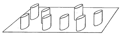
前記表面配列構造が、前記所望の配列を生成する形状及び/又は配向を有する特徴のランダムまたは疑似ランダムな二次元アレイからなる、液晶デバイス。
3.前記第二のセル壁の内側表面が、前記液晶材料の局部的ホメオトロピック配列を生ずるように処理され、それにより前記セルがハイブリッド配列ネマチックモードで作用する、上記2に記載のデバイス。
4.前記第二のセル壁の内側表面が、前記第一のセル壁上の配列方向に対して実質的に直角をなして、前記液晶材料の局部的プレーナー型又は傾斜プレーナー型の配列を生ずるように処理され、それにより前記セルがTNまたはSTNモードで作用する、上記2に記載のデバイス。
5.前記特徴の幾何学的形状及び間隔が、前記液晶材料に局部的なホメオトロピック配列をとらせるようなものである、上記1に記載のデバイス。
6.前記特徴が、単一の方位角方向において液晶ダイレクタの実質的に一様なプレーナー型又は傾斜プレーナー型の配列を生ずるように形成され及び/又は配向されている、上記1に記載のデバイス。
7.前記特徴が、複数の方位角方向において液晶ダイレクタの実質的に一様なプレーナー型又は傾斜プレーナー型の配列を生ずるように形成され及び/又は配向されている、上記1に記載のデバイス。
8.前記特徴が前記第一のセル壁の平面の法線に対して傾斜しているポストからなる、上記1に記載のデバイス。
9.前記セル壁に設けられた検光子及び偏光子をさらに含む、上記1に記載のデバイス。
10.前記特徴が、前記デバイスの異なる領域において異なる高さ、異なる形状、異なる傾斜、及び/又は異なる配向を有する、上記1に記載のデバイス。
11.前記ポストの傾斜角及び配向が、前記デバイス全体にわたって一様である、上記1に記載のデバイス。
12.上記1による液晶デバイスの製造に使用するセル壁であって、壁と、その一方の表面上にあり液晶材料のダイレクタを整列させるための配列表面ミクロ構造とからなり、前記ミクロ構造が前記所望の配列を生成する形状及び/又は配向を有する特徴のランダムまたは疑似ランダムな二次元アレイからなる、セル壁。
13.上記12によるセル壁を製造する方法であって、壁の表面にフォトレジスト材料を適用し、適用されたフォトレジスト材料を、ランダムまたは疑似ランダムな二次元アレイパターンを有するマスクを通して適切な光源に露光し、未露光のフォトレジスト材料を除去し、露光されたフォトレジスト材料を硬化して、前記壁上に配列特徴のランダムまたは疑似ランダムな二次元アレイを形成することからなる方法。
14.上記12によるセル壁を製造する方法であって、壁の表面にプラスチック材料を適用し、このプラスチック材料に配列特徴のランダムまたは疑似ランダムな二次元アレイをエンボス加工することからなる方法。
15.上記1による液晶デバイスを製造する方法であって、上記11による第一のセル壁を第二のセル壁に対して固着し、離間したセル壁を有しその内側表面の各々が少なくとも一つの電極構造を担持するセルを生成すべく、前記セル壁の少なくとも一方が電極構造を有するようにし、前記セルを液晶材料で充填し、前記セルをシールすることからなる方法。
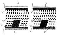
4 第二のセル壁
6 検光子
8 偏光子
10 四角形のポスト
12 行電極
14 列電極
Claims (13)
- 液晶材料の層を囲む第一のセル壁及び第二のセル壁と、前記液晶材料の少なくとも幾らかに電場を加えるための電極と、液晶分子に所望の配列を付与するための、少なくとも前記第一のセル壁の内側表面上の表面配列構造とからなる液晶デバイスであって、
前記表面配列構造が、前記所望の配列を生成する形状及び/又は配向を有するポストのランダムまたは疑似ランダムな二次元アレイからなり、前記ポストが、三角形、四角形、円形、楕円形又は多角形の断面を有し、対角線又は軸線の1つに沿って、前記第一のセル壁の平面の法線に対して傾斜しており、四角形の断面を有する場合には、対角線の1つに沿って傾斜している、液晶デバイス。
- 前記ポストの幾何学的形状及び間隔が、前記液晶材料に局部的なプレーナー型又は傾斜プレーナー型の配列をとらせるようなものである、請求項1に記載のデバイス。
- 前記第二のセル壁の内側表面が、前記液晶材料の局部的ホメオトロピック配列を生ずるように処理され、それにより前記セルがハイブリッド配列ネマチックモードで作用する、請求項2に記載のデバイス。
- 前記第二のセル壁の内側表面が、前記第一のセル壁上の配列方向に対して実質的に直角をなして、前記液晶材料の局部的プレーナー型又は傾斜プレーナー型の配列を生ずるように処理され、それにより前記セルがTNまたはSTNモードで作用する、請求項2に記載のデバイス。
- 前記ポストの幾何学的形状及び間隔が、前記液晶材料に局部的なホメオトロピック配列をとらせるようなものである、請求項1に記載のデバイス。
- 前記ポストが、単一の方位角方向において液晶ダイレクタの実質的に一様なプレーナー型又は傾斜プレーナー型の配列を生ずるように形成され及び/又は配向されている、請求項1に記載のデバイス。
- 前記セル壁に設けられた検光子及び偏光子をさらに含む、請求項1に記載のデバイス。
- 前記ポストが、前記デバイスの異なる領域において異なる高さ、異なる形状、異なる傾斜、及び/又は異なる配向を有する、請求項1に記載のデバイス。
- 前記ポストの傾斜角及び配向が、前記デバイス全体にわたって一様である、請求項1に記載のデバイス。
- 請求項1による液晶デバイスの製造に使用するセル壁であって、壁と、その一方の表面上にあり液晶材料のダイレクタを整列させるための配列表面ミクロ構造とからなり、前記ミクロ構造が前記所望の配列を生成する形状及び/又は配向を有するポストのランダムまたは疑似ランダムな二次元アレイからなり、前記ポストが、三角形、四角形、円形、楕円形又は多角形の断面を有し、対角線又は軸線の1つに沿って、前記第一のセル壁の平面の法線に対して傾斜しており、四角形の断面を有する場合には、対角線の1つに沿って傾斜している、セル壁。
- 請求項10によるセル壁を製造する方法であって、壁の表面にフォトレジスト材料を適用し、適用されたフォトレジスト材料を、ランダムまたは疑似ランダムな二次元アレイパターンを有するマスクを通して適切な光源に露光し、未露光のフォトレジスト材料を除去し、露光されたフォトレジスト材料を硬化して、前記壁上に配列ポストのランダムまたは疑似ランダムな二次元アレイを形成することからなる方法。
- 請求項10によるセル壁を製造する方法であって、壁の表面にプラスチック材料を適用し、このプラスチック材料に配列ポストのランダムまたは疑似ランダムな二次元アレイをエンボス加工することからなる方法。
- 請求項1による液晶デバイスを製造する方法であって、請求項10による第一のセル壁を第二のセル壁に対して固着し、離間したセル壁を有しその内側表面の各々が少なくとも一つの電極構造を担持するセルを生成すべく、前記セル壁の少なくとも一方が電極構造を有するようにし、前記セルを液晶材料で充填し、前記セルをシールすることからなる方法。
Applications Claiming Priority (2)
| Application Number | Priority Date | Filing Date | Title |
|---|---|---|---|
| EP00302480A EP1139152A1 (en) | 2000-03-27 | 2000-03-27 | Liquid crystal alignment structure |
| EP00302480.9 | 2000-03-27 |
Publications (3)
| Publication Number | Publication Date |
|---|---|
| JP2001281659A JP2001281659A (ja) | 2001-10-10 |
| JP2001281659A5 JP2001281659A5 (ja) | 2008-05-15 |
| JP5225526B2 true JP5225526B2 (ja) | 2013-07-03 |
Family
ID=8172828
Family Applications (1)
| Application Number | Title | Priority Date | Filing Date |
|---|---|---|---|
| JP2001090213A Expired - Fee Related JP5225526B2 (ja) | 2000-03-27 | 2001-03-27 | 液晶デバイス |
Country Status (5)
| Country | Link |
|---|---|
| US (2) | US6798481B2 (ja) |
| EP (1) | EP1139152A1 (ja) |
| JP (1) | JP5225526B2 (ja) |
| KR (1) | KR100794888B1 (ja) |
| DE (1) | DE60111990T2 (ja) |
Families Citing this family (19)
| Publication number | Priority date | Publication date | Assignee | Title |
|---|---|---|---|---|
| EP1139150A1 (en) * | 2000-03-27 | 2001-10-04 | Hewlett-Packard Company, A Delaware Corporation | Liquid crystal alignment structure |
| KR100670058B1 (ko) * | 2000-03-30 | 2007-01-16 | 삼성전자주식회사 | 액정 표시 장치 |
| KR100818193B1 (ko) * | 2000-07-05 | 2008-04-01 | 롤리크 아게 | 네마틱 액정 전기광학 소자 및 장치 |
| GB0017953D0 (en) * | 2000-07-21 | 2000-09-13 | Secr Defence | Liquid crystal device |
| TW554221B (en) * | 2001-01-09 | 2003-09-21 | Matsushita Electric Ind Co Ltd | Liquid crystal display device and manufacturing method thereof |
| EP1271225A1 (en) * | 2001-06-22 | 2003-01-02 | Hewlett-Packard Company, A Delaware Corporation | Bistable nematic liquid crystal device |
| KR20040093052A (ko) * | 2002-02-15 | 2004-11-04 | 다이니폰 인사츠 가부시키가이샤 | 배향막, 배향막의 제조 방법, 배향막이 부착된 기판 및액정 표시 장치 |
| JP2004212608A (ja) * | 2002-12-27 | 2004-07-29 | Dainippon Printing Co Ltd | 液晶表示装置およびその製造方法 |
| DE10318157A1 (de) | 2003-04-17 | 2004-11-11 | Leonhard Kurz Gmbh & Co. Kg | Folie und optisches Sicherungselement |
| GB2411735A (en) * | 2004-03-06 | 2005-09-07 | Sharp Kk | Control of liquid crystal alignment in an optical device |
| DE102004037365B4 (de) * | 2004-07-30 | 2011-12-01 | Deutsche Post Ag | Behälter mit elektronischem Etikett; Verwendung eines elektronischen Etiketts zur Kennzeichnung von Behältern |
| KR101143003B1 (ko) | 2005-05-16 | 2012-05-08 | 삼성전자주식회사 | 액정 표시 장치 |
| US8111368B2 (en) * | 2006-02-28 | 2012-02-07 | Hewlett-Packard Development Company, L.P. | Liquid crystal display |
| JP4923866B2 (ja) * | 2006-08-30 | 2012-04-25 | ソニー株式会社 | 液晶表示装置および映像表示装置 |
| JP5234303B2 (ja) * | 2006-10-13 | 2013-07-10 | Nltテクノロジー株式会社 | 表示装置、および電子機器 |
| JP5093717B2 (ja) * | 2006-10-23 | 2012-12-12 | Nltテクノロジー株式会社 | 光学素子およびこれを用いた照明光学装置、表示装置、電子機器 |
| JP5875068B2 (ja) * | 2012-03-08 | 2016-03-02 | 国立大学法人 奈良先端科学技術大学院大学 | 棒状分子の分子長分布の狭小化方法 |
| IL310194A (en) | 2016-11-18 | 2024-03-01 | Magic Leap Inc | Liquid crystal refraction lattices vary spatially |
| US11067860B2 (en) * | 2016-11-18 | 2021-07-20 | Magic Leap, Inc. | Liquid crystal diffractive devices with nano-scale pattern and methods of manufacturing the same |
Family Cites Families (42)
| Publication number | Priority date | Publication date | Assignee | Title |
|---|---|---|---|---|
| JPS542580B2 (ja) * | 1974-07-01 | 1979-02-09 | ||
| US4333708A (en) * | 1979-11-30 | 1982-06-08 | Bell Telephone Laboratories, Incorporated | Mechanically multistable liquid crystal cell |
| GB8608276D0 (en) * | 1986-04-04 | 1986-05-08 | British Telecomm | Optical devices |
| US4996123A (en) * | 1986-07-11 | 1991-02-26 | Matsushita Electric Industrial Co., Ltd. | Optically oriented photoresist pattern forming method using organic crystal in photoresist layer with specified refracting indices formula |
| JPH02137819A (ja) * | 1988-11-18 | 1990-05-28 | Matsushita Electric Ind Co Ltd | 液晶表示装置とその製造方法 |
| JPH02211422A (ja) * | 1989-02-13 | 1990-08-22 | Seiko Epson Corp | 液晶シャッター |
| JPH02226115A (ja) * | 1989-02-28 | 1990-09-07 | Citizen Watch Co Ltd | 強誘電性液晶素子の製造方法 |
| JPH03209220A (ja) * | 1990-01-11 | 1991-09-12 | Matsushita Electric Ind Co Ltd | 光学変調素子の製造法 |
| CA2049410C (en) * | 1990-08-17 | 2001-05-29 | Kiyofumi Takeuchi | Liquid crystal device and process for producing the same |
| JPH04225325A (ja) * | 1990-12-26 | 1992-08-14 | Victor Co Of Japan Ltd | 液晶分子配向体の製造方法 |
| KR970004881B1 (ko) * | 1991-07-08 | 1997-04-08 | 알프스 덴기 가부시기가이샤 | 액정의 배향막, 그 제조방법, 액정소자 및 그 제조방법 |
| JP3267989B2 (ja) | 1991-08-26 | 2002-03-25 | 株式会社東芝 | 液晶配向膜の製造方法 |
| JPH0580335A (ja) * | 1991-09-25 | 1993-04-02 | Toshiba Corp | 液晶表示素子および液晶配向膜の製造方法 |
| JPH0588177A (ja) * | 1991-09-30 | 1993-04-09 | Toshiba Corp | 液晶表示素子 |
| JPH06242447A (ja) * | 1993-02-18 | 1994-09-02 | Matsushita Electric Ind Co Ltd | 液晶素子とその製造法 |
| EP0636917B1 (en) * | 1993-07-27 | 1998-09-30 | Sharp Kabushiki Kaisha | Liquid crystal display |
| EP0649046B1 (en) * | 1993-10-19 | 2001-07-11 | Sharp Kabushiki Kaisha | A liquid crystal display device and a production method for the same |
| GB9402517D0 (en) * | 1994-02-09 | 1994-03-30 | Secr Defence | Ferroelectric liquid crystal alignment |
| TW428116B (en) * | 1994-05-18 | 2001-04-01 | Matsushita Electric Ind Co Ltd | Liquid crystal display element and laminated phase difference plate used for the same |
| JPH08114804A (ja) * | 1994-10-14 | 1996-05-07 | Sharp Corp | 液晶表示素子およびその製造方法 |
| GB9502635D0 (en) * | 1995-02-10 | 1995-03-29 | Secr Defence | Liquid crystal device alignment |
| US5552611A (en) * | 1995-06-06 | 1996-09-03 | International Business Machines | Pseudo-random registration masks for projection lithography tool |
| JPH09105941A (ja) * | 1995-10-13 | 1997-04-22 | Stanley Electric Co Ltd | 液晶表示装置 |
| GB9521106D0 (en) * | 1995-10-16 | 1995-12-20 | Secr Defence | Bistable nematic liquid crystal device |
| US6236445B1 (en) * | 1996-02-22 | 2001-05-22 | Hughes Electronics Corporation | Method for making topographic projections |
| GB9607854D0 (en) * | 1996-04-16 | 1996-06-19 | Secr Defence | Liquid crystal device |
| JPH10213794A (ja) * | 1996-04-30 | 1998-08-11 | Nec Corp | 液晶表示装置 |
| KR100343224B1 (ko) * | 1996-08-21 | 2002-11-18 | 삼성전자 주식회사 | 액정표시장치의 제조방법 |
| JP3199677B2 (ja) * | 1997-11-20 | 2001-08-20 | セイコーエプソン株式会社 | 電気光学装置の製造方法 |
| JPH11160706A (ja) * | 1997-11-21 | 1999-06-18 | Stanley Electric Co Ltd | 液晶表示素子の製造方法 |
| JP3481843B2 (ja) * | 1997-12-26 | 2003-12-22 | シャープ株式会社 | 液晶表示装置 |
| JP3977513B2 (ja) | 1998-04-28 | 2007-09-19 | 東レ株式会社 | 分割配向用基板及びこれを用いた液晶表示装置 |
| JP3335578B2 (ja) * | 1998-06-30 | 2002-10-21 | シャープ株式会社 | 液晶表示装置およびその製造方法 |
| JP2000105376A (ja) * | 1998-09-29 | 2000-04-11 | Sharp Corp | 液晶表示装置 |
| US6519018B1 (en) * | 1998-11-03 | 2003-02-11 | International Business Machines Corporation | Vertically aligned liquid crystal displays and methods for their production |
| JP2000206535A (ja) * | 1999-01-12 | 2000-07-28 | Sony Corp | 透過型ハイブリッド配向液晶表示装置 |
| EP1028346A3 (en) * | 1999-02-12 | 2002-05-02 | Matsushita Electric Industrial Co., Ltd. | Liquid crystal element and manufacturing method thereof |
| EP1094103A1 (en) | 1999-10-19 | 2001-04-25 | Rolic AG | Topologically structured polymer coating |
| GB9928126D0 (en) | 1999-11-30 | 2000-01-26 | Secr Defence | Bistable nematic liquid crystal device |
| KR100777690B1 (ko) * | 1999-12-27 | 2007-11-21 | 삼성전자주식회사 | 액정 표시 장치 |
| KR100778839B1 (ko) * | 2000-02-24 | 2007-11-22 | 엘지.필립스 엘시디 주식회사 | 액정표시장치의 배향막 성형용 플레이트 및 이를 이용한액정배향방법 |
| US6867837B2 (en) * | 2001-01-23 | 2005-03-15 | Raytheon Company | Liquid crystal device and manufacturing method |
-
2000
- 2000-03-27 EP EP00302480A patent/EP1139152A1/en not_active Withdrawn
-
2001
- 2001-02-22 DE DE60111990T patent/DE60111990T2/de not_active Expired - Lifetime
- 2001-03-23 US US09/815,999 patent/US6798481B2/en not_active Expired - Fee Related
- 2001-03-27 JP JP2001090213A patent/JP5225526B2/ja not_active Expired - Fee Related
- 2001-03-27 KR KR1020010015981A patent/KR100794888B1/ko not_active IP Right Cessation
-
2004
- 2004-07-27 US US10/899,818 patent/US20040263735A1/en not_active Abandoned
Also Published As
| Publication number | Publication date |
|---|---|
| US20040263735A1 (en) | 2004-12-30 |
| DE60111990T2 (de) | 2006-06-01 |
| JP2001281659A (ja) | 2001-10-10 |
| US20010024255A1 (en) | 2001-09-27 |
| EP1139152A1 (en) | 2001-10-04 |
| KR20010090586A (ko) | 2001-10-18 |
| US6798481B2 (en) | 2004-09-28 |
| KR100794888B1 (ko) | 2008-01-14 |
| DE60111990D1 (de) | 2005-08-25 |
Similar Documents
| Publication | Publication Date | Title |
|---|---|---|
| JP5225526B2 (ja) | 液晶デバイス | |
| US7460200B2 (en) | Liquid crystal alignment | |
| KR100326965B1 (ko) | 액정 표시 장치와 이의 제조 방법, 및 기판과 이의 제조 방법 | |
| US6141074A (en) | Four domain pixel for liquid crystalline light modulating device | |
| JP3673045B2 (ja) | 光を用いたツイストネマチック液晶セルの製造方法 | |
| US7106410B2 (en) | Bistable nematic liquid crystal device comprising an array of upstanding alignment posts | |
| JPWO2008062682A1 (ja) | 液晶表示パネル及び液晶表示パネルの製造方法 | |
| JPH10513276A (ja) | 液晶装置の配向 | |
| US7633596B2 (en) | Liquid crystal alignment | |
| JPH09325373A (ja) | 液晶表示素子とその製造方法 | |
| JP2004505297A (ja) | 液晶素子 | |
| JP3939341B2 (ja) | 液晶デバイスの配向 | |
| JP4484422B2 (ja) | 双安定ネマティック液晶デバイス | |
| JP2004302260A (ja) | 液晶表示装置およびその製造方法 | |
| EP1139154B1 (en) | Liquid crystal alignment | |
| WO2010100920A1 (ja) | 液晶表示装置およびその製造方法 | |
| JPH0961822A (ja) | 液晶表示装置とその製造方法 | |
| EP1139153B1 (en) | Liquid crystal alignment | |
| EP1091237A1 (en) | Liquid crystal device | |
| JP2004144866A (ja) | 液晶セルおよび液晶デバイス |
Legal Events
| Date | Code | Title | Description |
|---|---|---|---|
| A521 | Request for written amendment filed |
Free format text: JAPANESE INTERMEDIATE CODE: A523 Effective date: 20080327 |
|
| A621 | Written request for application examination |
Free format text: JAPANESE INTERMEDIATE CODE: A621 Effective date: 20080327 |
|
| A977 | Report on retrieval |
Free format text: JAPANESE INTERMEDIATE CODE: A971007 Effective date: 20101005 |
|
| A131 | Notification of reasons for refusal |
Free format text: JAPANESE INTERMEDIATE CODE: A131 Effective date: 20101019 |
|
| A601 | Written request for extension of time |
Free format text: JAPANESE INTERMEDIATE CODE: A601 Effective date: 20110119 |
|
| A602 | Written permission of extension of time |
Free format text: JAPANESE INTERMEDIATE CODE: A602 Effective date: 20110124 |
|
| A521 | Request for written amendment filed |
Free format text: JAPANESE INTERMEDIATE CODE: A523 Effective date: 20110419 |
|
| A131 | Notification of reasons for refusal |
Free format text: JAPANESE INTERMEDIATE CODE: A131 Effective date: 20111213 |
|
| A601 | Written request for extension of time |
Free format text: JAPANESE INTERMEDIATE CODE: A601 Effective date: 20120313 |
|
| A602 | Written permission of extension of time |
Free format text: JAPANESE INTERMEDIATE CODE: A602 Effective date: 20120316 |
|
| A521 | Request for written amendment filed |
Free format text: JAPANESE INTERMEDIATE CODE: A523 Effective date: 20120613 |
|
| A711 | Notification of change in applicant |
Free format text: JAPANESE INTERMEDIATE CODE: A711 Effective date: 20120820 |
|
| TRDD | Decision of grant or rejection written | ||
| A01 | Written decision to grant a patent or to grant a registration (utility model) |
Free format text: JAPANESE INTERMEDIATE CODE: A01 Effective date: 20130305 |
|
| A61 | First payment of annual fees (during grant procedure) |
Free format text: JAPANESE INTERMEDIATE CODE: A61 Effective date: 20130313 |
|
| R150 | Certificate of patent or registration of utility model |
Free format text: JAPANESE INTERMEDIATE CODE: R150 |
|
| FPAY | Renewal fee payment (event date is renewal date of database) |
Free format text: PAYMENT UNTIL: 20160322 Year of fee payment: 3 |
|
| LAPS | Cancellation because of no payment of annual fees |