JP5201854B2 - Manufacturing method of organic EL panel - Google Patents
Manufacturing method of organic EL panel Download PDFInfo
- Publication number
- JP5201854B2 JP5201854B2 JP2007057244A JP2007057244A JP5201854B2 JP 5201854 B2 JP5201854 B2 JP 5201854B2 JP 2007057244 A JP2007057244 A JP 2007057244A JP 2007057244 A JP2007057244 A JP 2007057244A JP 5201854 B2 JP5201854 B2 JP 5201854B2
- Authority
- JP
- Japan
- Prior art keywords
- organic
- protective layer
- panel
- manufacturing
- laminated
- Prior art date
- Legal status (The legal status is an assumption and is not a legal conclusion. Google has not performed a legal analysis and makes no representation as to the accuracy of the status listed.)
- Active
Links
- 238000004519 manufacturing process Methods 0.000 title claims description 31
- 239000011241 protective layer Substances 0.000 claims description 65
- 238000005520 cutting process Methods 0.000 claims description 39
- 239000000463 material Substances 0.000 claims description 39
- 239000000758 substrate Substances 0.000 claims description 31
- 238000000034 method Methods 0.000 claims description 26
- 239000000853 adhesive Substances 0.000 claims description 17
- 230000001070 adhesive effect Effects 0.000 claims description 17
- 239000011347 resin Substances 0.000 claims description 6
- 229920005989 resin Polymers 0.000 claims description 6
- 238000000605 extraction Methods 0.000 claims description 4
- 229910010272 inorganic material Inorganic materials 0.000 claims description 3
- 239000011147 inorganic material Substances 0.000 claims description 3
- 238000003475 lamination Methods 0.000 claims description 2
- 239000011368 organic material Substances 0.000 claims 1
- 239000010410 layer Substances 0.000 description 39
- 230000015572 biosynthetic process Effects 0.000 description 12
- 239000011521 glass Substances 0.000 description 11
- KFZMGEQAYNKOFK-UHFFFAOYSA-N Isopropanol Chemical compound CC(C)O KFZMGEQAYNKOFK-UHFFFAOYSA-N 0.000 description 9
- 238000007789 sealing Methods 0.000 description 8
- 229910052581 Si3N4 Inorganic materials 0.000 description 7
- 238000010438 heat treatment Methods 0.000 description 7
- 230000005525 hole transport Effects 0.000 description 7
- HQVNEWCFYHHQES-UHFFFAOYSA-N silicon nitride Chemical compound N12[Si]34N5[Si]62N3[Si]51N64 HQVNEWCFYHHQES-UHFFFAOYSA-N 0.000 description 7
- 238000002347 injection Methods 0.000 description 6
- 239000007924 injection Substances 0.000 description 6
- 238000010586 diagram Methods 0.000 description 5
- 230000003287 optical effect Effects 0.000 description 5
- 150000002894 organic compounds Chemical class 0.000 description 5
- 238000007740 vapor deposition Methods 0.000 description 5
- QVGXLLKOCUKJST-UHFFFAOYSA-N atomic oxygen Chemical compound [O] QVGXLLKOCUKJST-UHFFFAOYSA-N 0.000 description 4
- 238000005336 cracking Methods 0.000 description 4
- 238000000151 deposition Methods 0.000 description 4
- 239000001301 oxygen Substances 0.000 description 4
- 229910052760 oxygen Inorganic materials 0.000 description 4
- 239000004033 plastic Substances 0.000 description 4
- 229920003023 plastic Polymers 0.000 description 4
- 238000012360 testing method Methods 0.000 description 4
- 230000008021 deposition Effects 0.000 description 3
- 229910003460 diamond Inorganic materials 0.000 description 3
- 239000010432 diamond Substances 0.000 description 3
- 239000011159 matrix material Substances 0.000 description 3
- 238000005268 plasma chemical vapour deposition Methods 0.000 description 3
- CSCPPACGZOOCGX-UHFFFAOYSA-N Acetone Chemical compound CC(C)=O CSCPPACGZOOCGX-UHFFFAOYSA-N 0.000 description 2
- 239000004925 Acrylic resin Substances 0.000 description 2
- 229920000178 Acrylic resin Polymers 0.000 description 2
- 238000004140 cleaning Methods 0.000 description 2
- 238000011156 evaluation Methods 0.000 description 2
- 239000000284 extract Substances 0.000 description 2
- -1 for example Substances 0.000 description 2
- 238000010030 laminating Methods 0.000 description 2
- 230000002093 peripheral effect Effects 0.000 description 2
- 238000000206 photolithography Methods 0.000 description 2
- 238000007781 pre-processing Methods 0.000 description 2
- 238000003825 pressing Methods 0.000 description 2
- 238000000926 separation method Methods 0.000 description 2
- 238000004544 sputter deposition Methods 0.000 description 2
- TVIVIEFSHFOWTE-UHFFFAOYSA-K tri(quinolin-8-yloxy)alumane Chemical compound [Al+3].C1=CN=C2C([O-])=CC=CC2=C1.C1=CN=C2C([O-])=CC=CC2=C1.C1=CN=C2C([O-])=CC=CC2=C1 TVIVIEFSHFOWTE-UHFFFAOYSA-K 0.000 description 2
- 239000002699 waste material Substances 0.000 description 2
- OKTJSMMVPCPJKN-UHFFFAOYSA-N Carbon Chemical compound [C] OKTJSMMVPCPJKN-UHFFFAOYSA-N 0.000 description 1
- 229920000089 Cyclic olefin copolymer Polymers 0.000 description 1
- UFHFLCQGNIYNRP-UHFFFAOYSA-N Hydrogen Chemical compound [H][H] UFHFLCQGNIYNRP-UHFFFAOYSA-N 0.000 description 1
- 239000004677 Nylon Substances 0.000 description 1
- CBENFWSGALASAD-UHFFFAOYSA-N Ozone Chemical compound [O-][O+]=O CBENFWSGALASAD-UHFFFAOYSA-N 0.000 description 1
- VYPSYNLAJGMNEJ-UHFFFAOYSA-N Silicium dioxide Chemical compound O=[Si]=O VYPSYNLAJGMNEJ-UHFFFAOYSA-N 0.000 description 1
- GWEVSGVZZGPLCZ-UHFFFAOYSA-N Titan oxide Chemical compound O=[Ti]=O GWEVSGVZZGPLCZ-UHFFFAOYSA-N 0.000 description 1
- 230000005856 abnormality Effects 0.000 description 1
- 229910021417 amorphous silicon Inorganic materials 0.000 description 1
- FJDQFPXHSGXQBY-UHFFFAOYSA-L caesium carbonate Chemical compound [Cs+].[Cs+].[O-]C([O-])=O FJDQFPXHSGXQBY-UHFFFAOYSA-L 0.000 description 1
- 229910000024 caesium carbonate Inorganic materials 0.000 description 1
- 229910052799 carbon Inorganic materials 0.000 description 1
- 239000012461 cellulose resin Substances 0.000 description 1
- 238000010549 co-Evaporation Methods 0.000 description 1
- 230000000052 comparative effect Effects 0.000 description 1
- PMHQVHHXPFUNSP-UHFFFAOYSA-M copper(1+);methylsulfanylmethane;bromide Chemical compound Br[Cu].CSC PMHQVHHXPFUNSP-UHFFFAOYSA-M 0.000 description 1
- 239000006063 cullet Substances 0.000 description 1
- 230000006866 deterioration Effects 0.000 description 1
- 238000011161 development Methods 0.000 description 1
- SWXVUIWOUIDPGS-UHFFFAOYSA-N diacetone alcohol Natural products CC(=O)CC(C)(C)O SWXVUIWOUIDPGS-UHFFFAOYSA-N 0.000 description 1
- 238000010894 electron beam technology Methods 0.000 description 1
- 238000001704 evaporation Methods 0.000 description 1
- 230000008020 evaporation Effects 0.000 description 1
- 230000006355 external stress Effects 0.000 description 1
- 239000007789 gas Substances 0.000 description 1
- 239000001257 hydrogen Substances 0.000 description 1
- 229910052739 hydrogen Inorganic materials 0.000 description 1
- AMGQUBHHOARCQH-UHFFFAOYSA-N indium;oxotin Chemical compound [In].[Sn]=O AMGQUBHHOARCQH-UHFFFAOYSA-N 0.000 description 1
- 238000002955 isolation Methods 0.000 description 1
- 238000005304 joining Methods 0.000 description 1
- 238000004020 luminiscence type Methods 0.000 description 1
- 238000001755 magnetron sputter deposition Methods 0.000 description 1
- 239000012528 membrane Substances 0.000 description 1
- 238000012986 modification Methods 0.000 description 1
- 230000004048 modification Effects 0.000 description 1
- IBHBKWKFFTZAHE-UHFFFAOYSA-N n-[4-[4-(n-naphthalen-1-ylanilino)phenyl]phenyl]-n-phenylnaphthalen-1-amine Chemical compound C1=CC=CC=C1N(C=1C2=CC=CC=C2C=CC=1)C1=CC=C(C=2C=CC(=CC=2)N(C=2C=CC=CC=2)C=2C3=CC=CC=C3C=CC=2)C=C1 IBHBKWKFFTZAHE-UHFFFAOYSA-N 0.000 description 1
- 229920001778 nylon Polymers 0.000 description 1
- 239000012044 organic layer Substances 0.000 description 1
- TWNQGVIAIRXVLR-UHFFFAOYSA-N oxo(oxoalumanyloxy)alumane Chemical compound O=[Al]O[Al]=O TWNQGVIAIRXVLR-UHFFFAOYSA-N 0.000 description 1
- 229920005668 polycarbonate resin Polymers 0.000 description 1
- 239000004431 polycarbonate resin Substances 0.000 description 1
- 229920001225 polyester resin Polymers 0.000 description 1
- 239000004645 polyester resin Substances 0.000 description 1
- 229920001721 polyimide Polymers 0.000 description 1
- 239000009719 polyimide resin Substances 0.000 description 1
- 239000002952 polymeric resin Substances 0.000 description 1
- 229920005990 polystyrene resin Polymers 0.000 description 1
- 238000004080 punching Methods 0.000 description 1
- 229910052814 silicon oxide Inorganic materials 0.000 description 1
- OGIDPMRJRNCKJF-UHFFFAOYSA-N titanium oxide Inorganic materials [Ti]=O OGIDPMRJRNCKJF-UHFFFAOYSA-N 0.000 description 1
- XLYOFNOQVPJJNP-UHFFFAOYSA-N water Substances O XLYOFNOQVPJJNP-UHFFFAOYSA-N 0.000 description 1
Images

Classifications
-
- H—ELECTRICITY
- H10—SEMICONDUCTOR DEVICES; ELECTRIC SOLID-STATE DEVICES NOT OTHERWISE PROVIDED FOR
- H10K—ORGANIC ELECTRIC SOLID-STATE DEVICES
- H10K59/00—Integrated devices, or assemblies of multiple devices, comprising at least one organic light-emitting element covered by group H10K50/00
- H10K59/80—Constructional details
- H10K59/87—Passivation; Containers; Encapsulations
- H10K59/871—Self-supporting sealing arrangements
- H10K59/8722—Peripheral sealing arrangements, e.g. adhesives, sealants
-
- H—ELECTRICITY
- H10—SEMICONDUCTOR DEVICES; ELECTRIC SOLID-STATE DEVICES NOT OTHERWISE PROVIDED FOR
- H10K—ORGANIC ELECTRIC SOLID-STATE DEVICES
- H10K71/00—Manufacture or treatment specially adapted for the organic devices covered by this subclass
-
- H—ELECTRICITY
- H10—SEMICONDUCTOR DEVICES; ELECTRIC SOLID-STATE DEVICES NOT OTHERWISE PROVIDED FOR
- H10K—ORGANIC ELECTRIC SOLID-STATE DEVICES
- H10K50/00—Organic light-emitting devices
- H10K50/80—Constructional details
- H10K50/84—Passivation; Containers; Encapsulations
- H10K50/842—Containers
- H10K50/8426—Peripheral sealing arrangements, e.g. adhesives, sealants
-
- H—ELECTRICITY
- H10—SEMICONDUCTOR DEVICES; ELECTRIC SOLID-STATE DEVICES NOT OTHERWISE PROVIDED FOR
- H10K—ORGANIC ELECTRIC SOLID-STATE DEVICES
- H10K50/00—Organic light-emitting devices
- H10K50/80—Constructional details
- H10K50/84—Passivation; Containers; Encapsulations
- H10K50/844—Encapsulations
-
- H—ELECTRICITY
- H10—SEMICONDUCTOR DEVICES; ELECTRIC SOLID-STATE DEVICES NOT OTHERWISE PROVIDED FOR
- H10K—ORGANIC ELECTRIC SOLID-STATE DEVICES
- H10K59/00—Integrated devices, or assemblies of multiple devices, comprising at least one organic light-emitting element covered by group H10K50/00
- H10K59/80—Constructional details
- H10K59/87—Passivation; Containers; Encapsulations
- H10K59/873—Encapsulations
-
- H—ELECTRICITY
- H10—SEMICONDUCTOR DEVICES; ELECTRIC SOLID-STATE DEVICES NOT OTHERWISE PROVIDED FOR
- H10K—ORGANIC ELECTRIC SOLID-STATE DEVICES
- H10K71/00—Manufacture or treatment specially adapted for the organic devices covered by this subclass
- H10K71/40—Thermal treatment, e.g. annealing in the presence of a solvent vapour
-
- H—ELECTRICITY
- H10—SEMICONDUCTOR DEVICES; ELECTRIC SOLID-STATE DEVICES NOT OTHERWISE PROVIDED FOR
- H10K—ORGANIC ELECTRIC SOLID-STATE DEVICES
- H10K71/00—Manufacture or treatment specially adapted for the organic devices covered by this subclass
- H10K71/851—Division of substrate
-
- Y—GENERAL TAGGING OF NEW TECHNOLOGICAL DEVELOPMENTS; GENERAL TAGGING OF CROSS-SECTIONAL TECHNOLOGIES SPANNING OVER SEVERAL SECTIONS OF THE IPC; TECHNICAL SUBJECTS COVERED BY FORMER USPC CROSS-REFERENCE ART COLLECTIONS [XRACs] AND DIGESTS
- Y10—TECHNICAL SUBJECTS COVERED BY FORMER USPC
- Y10T—TECHNICAL SUBJECTS COVERED BY FORMER US CLASSIFICATION
- Y10T156/00—Adhesive bonding and miscellaneous chemical manufacture
- Y10T156/10—Methods of surface bonding and/or assembly therefor
- Y10T156/1052—Methods of surface bonding and/or assembly therefor with cutting, punching, tearing or severing
- Y10T156/1056—Perforating lamina
- Y10T156/1057—Subsequent to assembly of laminae
Landscapes
- Physics & Mathematics (AREA)
- Optics & Photonics (AREA)
- Engineering & Computer Science (AREA)
- Manufacturing & Machinery (AREA)
- Electroluminescent Light Sources (AREA)
Description
本発明は、有機ELパネルの製造方法に係わる。 The present invention relates to a method for manufacturing an organic EL panel.
ガラス基板上に有機発光層が二つの電極の間に挟まれたサンドイッチ構造の有機EL素子を有する有機ELパネルが知られている。そして、前記有機発光層の光を外に取り出せるようにするために、電極の片方は透明のものが使われており、一般的にはITO(Indium Tin Oxide)などの透明電極が使われている。更に前記有機発光層の外周面は封止部材により封止され、外部駆動回路により電圧を印加することにより発光する。 An organic EL panel having an organic EL element having a sandwich structure in which an organic light emitting layer is sandwiched between two electrodes on a glass substrate is known. In order to extract light from the organic light emitting layer to the outside, one of the electrodes is transparent, and generally a transparent electrode such as ITO (Indium Tin Oxide) is used. . Furthermore, the outer peripheral surface of the organic light emitting layer is sealed with a sealing member, and emits light when a voltage is applied by an external drive circuit.
以上の原理により発光する有機EL素子を有する有機ELパネルは、視認性に優れ且つ発色性が多様であることから、車載用コンポや携帯電話等のディスプレイや表示素子に利用されている。 An organic EL panel having an organic EL element that emits light based on the above principle is excellent in visibility and has a wide variety of color development properties. Therefore, the organic EL panel is used for displays and display elements such as in-vehicle components and mobile phones.
有機ELパネルの製造において、近年有機ELパネルを多面取りで生産する方法が考え出されている。この方法は、一枚の大型基板上に複数のパネルに対応した有機EL発光部を作成した後に、基板を切断して一枚の有機ELパネルを得る方法である。 In the manufacture of organic EL panels, in recent years, a method for producing organic EL panels with multiple layouts has been devised. In this method, an organic EL light emitting unit corresponding to a plurality of panels is formed on a single large substrate, and then the substrate is cut to obtain a single organic EL panel.
このような有機ELパネルの製造方法として特許文献1が知られている。特許文献1に記載の有機ELパネルの製造方法は、封止膜を形成した部分で基板をカットすると封止膜にひび割れや剥がれが発生する虞があることを課題としている。そこで、マスク部材をカットライン上に配置した状態で封止膜を形成し、マスク部材の除去によってカットライン上に封止膜がない状態で基板をカットすることによって上記課題の解決を図っている。封止膜は水及び酸素等の透過を阻止することを目的として形成されている。
しかしながら、特許文献1に記載の有機ELパネルの製造方法は、カットライン上にマスク部材を精度良く配置しなければならず、また封止膜を形成した後にマスク部材を剥がす工程を要するため、製造プロセスが複雑になる。
However, the manufacturing method of the organic EL panel described in
製造プロセスを簡単にするためには、大型基材上に配置される複数の有機EL素子群の間を跨いで封止膜等の保護層を形成し、保護層を大型基材とともに切断することが必要である。 In order to simplify the manufacturing process, a protective layer such as a sealing film is formed across a plurality of organic EL element groups arranged on a large substrate, and the protective layer is cut together with the large substrate. is necessary.
そこで、本発明は、特許文献1の発明と同様に保護層の切断によって保護層にひび割れや剥がれが発生する課題を解決しつつ、特許文献1の発明では困難であった製造プロセスを簡単にすることを目的とする。
Therefore, the present invention simplifies the manufacturing process that was difficult in the invention of
本発明は、基材と、前記基材の上に配置されている複数の有機EL素子を有する有機EL素子群と、前記有機EL素子群の上に配置されている透明性を有する無機物からなる保護層と、を有する有機ELパネルを、
前記有機EL素子群が複数配置されている部材の前記複数の有機EL素子群の間で、前記基材と前記保護層とを切断することによって得る有機ELパネルの製造方法において、有機樹脂からなる積層部材を前記保護層の上に接して前記複数の有機EL素子群の間を跨いで配置する工程と、
前記基材と、前記積層部材が配置された前記保護層とを、前記複数の有機EL素子群の間で前記基材側から切断する工程と、
を有することを特徴とする有機ELパネルの製造方法を提供する。
The present invention comprises a base material, an organic EL element group having a plurality of organic EL elements disposed on the base material, and a transparent inorganic material disposed on the organic EL element group. An organic EL panel having a protective layer,
In the manufacturing method of the organic electroluminescent panel obtained by cut | disconnecting the said base material and the said protective layer between the said some organic EL element group of the member in which the said plurality of organic EL element groups are arrange | positioned, it consists of organic resin. Placing the laminated member on the protective layer and straddling the plurality of organic EL element groups; and
Cutting the base material and the protective layer on which the laminated member is disposed from the base material side between the plurality of organic EL element groups;
The manufacturing method of the organic electroluminescent panel characterized by having.
本発明によれば、保護層の上に接して積層部材を配置した上で基材側から基材および保護層を切断するため、保護層を切断する際に生じるひび割れや剥がれを積層部材によって妨げることができる。また、保護層を基材とともに切断するため、基材の切断と保護層の切断を別々に行う必要がなく、製造プロセスを簡単にすることができる。
したがって本発明は、保護層にひび割れや剥がれの少ない有機ELパネルを簡単な方法で提供することができる。
According to the present invention, since the laminated member is disposed on and in contact with the protective layer, the substrate and the protective layer are cut from the substrate side, so that the laminated member prevents cracking or peeling that occurs when the protective layer is cut. be able to. Further, since the protective layer is cut together with the base material, it is not necessary to separately cut the base material and the protective layer, and the manufacturing process can be simplified.
Therefore, this invention can provide the organic EL panel with few cracks and peeling in a protective layer by a simple method.
本発明は、基材と、基材上に配置される複数の有機EL素子を有する有機EL素子群と、有機EL素子群の上に配置される保護層と、を有する有機ELパネルの製造方法である。この製造方法は、有機EL素子群が複数配置されている部材の複数の有機EL素子群の間で、基材と保護層とを切断するものである。 The present invention relates to a method for producing an organic EL panel having a base material, an organic EL element group having a plurality of organic EL elements disposed on the base material, and a protective layer disposed on the organic EL element group. It is. In this manufacturing method, a base material and a protective layer are cut between a plurality of organic EL element groups of a member in which a plurality of organic EL element groups are arranged.
そして、本発明は、複数の有機EL素子群の間を跨いで保護層の上に接して積層部材を配置する工程と、基材と上に前記積層部材が配置された保護層とを、複数の有機EL素子群の間で基材側から切断する工程と、を有することを特徴とする。 The present invention includes a step of placing a laminated member in contact with the protective layer across a plurality of organic EL element groups, and a plurality of protective layers on which the laminated member is arranged. And a step of cutting from the substrate side between the organic EL element groups.
保護層の上に接して積層部材が配置されているため、基材側から保護層を切断する際に保護層は積層部材によって固定されるため、保護層に加わる力の一部は積層部材に伝わる。保護層に余分な力が加わることを積層部材が妨げるため、保護層にひび割れや剥がれが発生しにくくなる。そして、ひび割れや、剥がれが発生した部分から水分等が有機EL素子に浸入することを防ぐことができ、より長時間に渡って高品質な発光を維持できる有機ELパネルを提供することができる。 Since the laminated member is disposed on and in contact with the protective layer, the protective layer is fixed by the laminated member when the protective layer is cut from the base material side, so a part of the force applied to the protective layer is applied to the laminated member. It is transmitted. Since the laminated member prevents an extra force from being applied to the protective layer, the protective layer is unlikely to be cracked or peeled off. In addition, it is possible to prevent moisture and the like from entering the organic EL element from the portion where cracking or peeling occurs, and it is possible to provide an organic EL panel that can maintain high-quality light emission for a longer time.
また、本発明では、積層部材が保護層の上に配置された状態で切断を行うため、切断によって発生する切断カスが保護層表面に付着しなくなる。保護層を配置した状態で切断を行った後に積層部材を配置する場合には、切断カスが保護層表面に付着してしまうため、切断カスを除去する別の工程が必要になる。また、切断カスが付着したまま積層部材を配置すると、切断カスが保護層を傷つけてしまい、また基材とは反対側から光を取り出すトップエミッション型の有機ELパネルの場合には表示品位を著しく低下させてしまう。本発明の製造方法はこのような問題を発生させることなく、有機ELパネルを製造することが可能である。 Moreover, in this invention, since it cut | disconnects in the state in which the lamination | stacking member has been arrange | positioned on a protective layer, the cutting waste generated by cutting | disconnection does not adhere to the protective layer surface. When the laminated member is disposed after being cut in a state where the protective layer is disposed, the cutting residue adheres to the surface of the protective layer, and thus another step for removing the cutting residue is required. In addition, if the laminated member is placed with the cutting residue attached, the cutting residue damages the protective layer, and the display quality is remarkably improved in the case of a top emission type organic EL panel that extracts light from the side opposite to the substrate. It will decrease. The production method of the present invention can produce an organic EL panel without causing such problems.
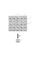
以下、本発明に係る有機ELパネルの構成及び有機ELパネルの製造方法を図面に基づいて説明する。図1及び図2は、本発明に係る有機ELパネルの製造方法の1実施形態を説明する図であり、図1は切断対象となる部材の断面模式図であり、図2は切断対象となる部材の平面模式図である。
図1及び図2において、1は基材、2は有機EL素子群、3は保護層、4は接着部材(積層部材)、5は平面部材、6は外部接続端子、7は切断ラインである。
Hereinafter, a configuration of an organic EL panel and a method for manufacturing the organic EL panel according to the present invention will be described with reference to the drawings. 1 and 2 are diagrams for explaining an embodiment of a method for producing an organic EL panel according to the present invention. FIG. 1 is a schematic cross-sectional view of a member to be cut, and FIG. 2 is to be cut. It is a plane schematic diagram of a member.
1 and 2, 1 is a base material, 2 is an organic EL element group, 3 is a protective layer, 4 is an adhesive member (laminated member), 5 is a planar member, 6 is an external connection terminal, and 7 is a cutting line. .
本発明に係る有機ELパネルの製造方法において、切断の対象となるものは図1に示すように、複数の有機ELパネルに共通する基材1上に有機EL素子群2が間隔をあけて複数配置されている。そして、有機EL素子群2の間を跨いで複数の有機EL素子群2の上に保護層3が配置されていて、有機EL素子群2の間を跨いで保護層3の上に接して積層部材4が配置されている。そして、これらの部材からなる切断対象を複数の有機EL素子群2の間において基材側から切断する。
In the method of manufacturing an organic EL panel according to the present invention, as shown in FIG. 1, a plurality of organic EL element groups 2 are spaced apart on a
基材1は、有機EL素子を構成する一対の電極、及び電極間に配置される有機化合物層を配置する土台となる部材である。例えば、ガラスや有機樹脂等の部材を有するものであって、アクティブマトリクス型の有機ELパネルの場合には、ガラスや有機樹脂等の部材の他にTFT等の回路素子や平坦化層等を有するものであっても良い。
The
有機EL素子群2は、複数の有機EL素子の集合である。有機EL素子とは一対の電極間に有機化合物層が配置されていて、電極間に電流を流すことによって、有機化合物層から発光が取り出されるものである。パッシブマトリクス型の有機ELパネルの場合には、ストライプ状の電極が交差した点を有機EL素子とし、複数の交差した点の集合が有機EL素子群となる。アクティブマトリクス型の有機ELパネルの場合には、素子を駆動するTFT等の回路素子に接続された電極とそれに対向して配置される電極部分と、電極間の有機化合物層の発光部分とが有機EL素子となる。そして、その有機EL素子が複数配置されたものを有機EL素子群となる。 The organic EL element group 2 is a set of a plurality of organic EL elements. In the organic EL element, an organic compound layer is disposed between a pair of electrodes, and light is extracted from the organic compound layer by passing a current between the electrodes. In the case of a passive matrix type organic EL panel, a point where stripe-shaped electrodes intersect is an organic EL element, and a set of a plurality of intersecting points is an organic EL element group. In the case of an active matrix type organic EL panel, an electrode connected to a circuit element such as a TFT for driving the element, an electrode portion disposed opposite thereto, and a light emitting portion of an organic compound layer between the electrodes are organic. It becomes an EL element. A plurality of organic EL elements are arranged as an organic EL element group.
保護層3は、有機EL素子を水分・酸素の影響から守り、その劣化を低減するために設けられる層である。材料としては例えば、酸化珪素、窒化珪素、酸化アルミニウム、窒化アルミニウム、酸化チタン、アモルファスシリコン、ダイアモンド状カーボン、SiCN等の無機物が好適であり、中でも窒化珪素が防湿性、成膜性、耐クラック性に優れているため好んで用いられる。また、基材とは反対側から光を取り出すトップエミッションタイプの有機ELパネルの場合は、保護層3を介して光が取り出されるため、透明性も要求される。窒化珪素は僅かに着色しているので、透明性を上げるために水素をドープすることが好ましい。 The protective layer 3 is a layer provided in order to protect the organic EL element from the influence of moisture and oxygen and reduce the deterioration thereof. As materials, for example, inorganic materials such as silicon oxide, silicon nitride, aluminum oxide, aluminum nitride, titanium oxide, amorphous silicon, diamond-like carbon, and SiCN are suitable. Among them, silicon nitride is moisture-proof, film-forming, and crack-resistant. It is preferably used because of its excellent resistance. Further, in the case of a top emission type organic EL panel that extracts light from the side opposite to the base material, since light is extracted through the protective layer 3, transparency is also required. Since silicon nitride is slightly colored, it is preferable to dope hydrogen to increase transparency.
保護層の厚みは、500〜10000nmであることが好ましい。500nm未満であるとピンホールなどにより十分な防湿性が発揮できず、10000nmを超えると外部応力によるクラックの発生が起こりやすくなる。 The thickness of the protective layer is preferably 500 to 10,000 nm. If it is less than 500 nm, sufficient moisture resistance cannot be exhibited due to pinholes or the like, and if it exceeds 10000 nm, cracks are likely to occur due to external stress.
上記防湿層の形成方法としては、プラズマCVD法、抵抗加熱蒸着法、電子ビーム蒸着法、スパッタリング法などから選択すればよい。窒化珪素の場合はプラズマCVD法によるのが一般的である。 A method for forming the moisture-proof layer may be selected from plasma CVD, resistance heating vapor deposition, electron beam vapor deposition, and sputtering. In the case of silicon nitride, the plasma CVD method is generally used.
接着部材4は、保護層3上に平面部材5を接着させるための部材である。本実施の形態においては、接着部材4が保護層3の上に接して配置される積層部材となる。積層部材が保護層3を固定し、ひび割れや剥がれの発生を妨げる。積層部材は保護層3を切断する際にひび割れや剥がれを起こして積層部材と同時に切断されないように、脆性の低い材料であることが好ましく、具体的には有機樹脂等の部材が好ましく用いられる。また、積層部材は保護層の表面を、切断に用いられる刃等の部材から保護する。積層部材は、有機ELパネルの光取り出し側に配置されていてもよいし、光取り出し側とは反対側に配置されていても良い。光取り出し側に配置されている場合には、前述したように、切断カスによって表示品位を著しく低下させることを回避することができる。なお、本実施の形態では、積層部材は保護層3上に平面部材5を接着させる接着部材4であるが、必ずしも、接着部材でなくてもよく、保護層3上に積層部材が単独で配置されてもよい。 The adhesive member 4 is a member for bonding the planar member 5 on the protective layer 3. In the present embodiment, the adhesive member 4 is a laminated member disposed in contact with the protective layer 3. The laminated member fixes the protective layer 3 and prevents the occurrence of cracks and peeling. The laminated member is preferably made of a material having low brittleness so that cracking or peeling is not caused when the protective layer 3 is cut, and specifically, a member such as an organic resin is preferably used. Further, the laminated member protects the surface of the protective layer from members such as blades used for cutting. The laminated member may be disposed on the light extraction side of the organic EL panel, or may be disposed on the side opposite to the light extraction side. In the case where it is arranged on the light extraction side, it is possible to avoid a significant reduction in display quality due to the cutting residue as described above. In the present embodiment, the laminated member is the adhesive member 4 that adheres the planar member 5 on the protective layer 3, but it is not necessarily an adhesive member, and the laminated member is disposed alone on the protective layer 3. May be.
平面部材5は、本発明においては必ずしも設けられる必要はないが、保護層3を基材1側から切断する際に保護層3をより強固に固定することになるため、設けられていることが好ましい。平面部材5が設けられる場合には、平面部材5は例えば、防湿層の保護、防湿性のさらなる付与、切断して得られるパネルの機械的強度向上、光学特性の向上などを目的とする部材であってもよい。材料としては例えば、ガラス、プラスチックが好適であり、後述する開口部が設け易いという点で、プラスチックがより好適である。具体的には、フッ素樹脂、アクリル樹脂、ポリエステル樹脂、ポリカーボネート樹脂、ナイロン樹脂、アセチル化セルロース樹脂、環状オレフィン重合体樹脂、ポリスチレン樹脂などの透明性に優れるプラスチックが好ましい。また、複数の材料の積層体でもよい。
The planar member 5 is not necessarily provided in the present invention, but may be provided because the protective layer 3 is more firmly fixed when the protective layer 3 is cut from the
また、平面部材5は円偏光部材であっても良い。円偏光部材は外光反射を低減するための部材であって偏光部材(直線偏光部材)と位相差部材とが積層されたものである。 Further, the planar member 5 may be a circularly polarizing member. The circularly polarizing member is a member for reducing external light reflection, and a polarizing member (linearly polarizing member) and a retardation member are laminated.
外部接続端子6は、駆動回路部を有機ELパネルに電気的に接続し、有機ELパネルに電気信号の入出力を行うために、有機ELパネル側に設けられる外部接続端子のことである。一般的に、外部接続端子6には駆動回路部側の端子としてフレキシブルプリント配線板(FPC)が接合される。外部接続端子6は基材1に設けられているため、基材1上に積層される保護層3や積層部材は外部接続端子6上には設けられず、外部接続端子6が露出している必要がある。そのため、積層部材の外部接続端子6に対応する位置に開口を設けて、開口を設けた積層部材を保護層3の上に接して配置することが好ましい。積層部材に開口を設けるためには、まず積層部材を平面部材に配置して、積層部材が設けられた平面部材の外部接続端子6に対応する位置に開口を設ける。そして、開口が設けられた積層部材および平面部材を保護層3の上に接して配置する。この方法は、積層部材を保護層3の上に配置した後に外部接続端子6に対応する部分を切り取る方法よりも、製造プロセスを大幅に簡単にすることができる。
The external connection terminal 6 is an external connection terminal provided on the organic EL panel side in order to electrically connect the drive circuit unit to the organic EL panel and to input / output electric signals to / from the organic EL panel. Generally, a flexible printed wiring board (FPC) is joined to the external connection terminal 6 as a terminal on the drive circuit unit side. Since the external connection terminal 6 is provided on the
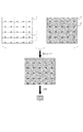
次に、本発明の有機ELパネルの製造方法を図3を用いてより詳細に説明する。図3において、8は有機EL素子基板、9は開口部である。
ガラス基材上に蒸着装置やスピンコーターなどの成膜装置により一対の電極と一対の電極間に配置される有機化合物層とからなる有機EL素子の複数からなる有機EL素子群を複数形成し、更に保護層3を形成する。
Next, the manufacturing method of the organic EL panel of the present invention will be described in more detail with reference to FIG. In FIG. 3, 8 is an organic EL element substrate, and 9 is an opening.
Forming a plurality of organic EL element groups consisting of a plurality of organic EL elements composed of a pair of electrodes and an organic compound layer disposed between the pair of electrodes by a film forming apparatus such as a vapor deposition apparatus or a spin coater on a glass substrate, Further, the protective layer 3 is formed.
次いで、フレキシブルプリント配線板(FPC)を接合するために設けられた電気信号入出力用の外部接続端子6に対応する部分に開口部9を有する平面部材5を接着部材4で有機EL素子群2が配置された基材1に貼り付ける。例えば、接着部材4として粘着剤を予め平面部材5に積層しておき、これをロールラミネート法や真空ラミネート法などによって有機EL素子群2が配置された基材1に貼り付ければよい。また、必要に応じて加熱しながら貼り付けてもよい。さらに、貼り付け後に接着部材4中の気泡を取り除くためにオートクレーブなどによって加熱加圧処理してもよい。
Subsequently, the planar member 5 having the opening 9 in the portion corresponding to the external connection terminal 6 for electric signal input / output provided for joining the flexible printed wiring board (FPC) is attached to the organic EL element group 2 by the adhesive member 4. Is affixed to the
こうして平面部材5を貼り付けたものを切断ライン7に沿って各パネル単位に切断する。本発明における切断とは、ダイサーやカッター等によって切断される対象に直接刃を入れて切断することだけではない。本発明における切断は、スクライバーによって切断される対象の表面に切り込みを入れた後に切り込み部に押圧を加えて分割することや、レーザーによる切断も含むものである。切断方法としては、切断される材料がガラスの場合はダイアモンドカッターやレーザーによる方法、プラスチックの場合は切り刃や抜き刃による方法などを種々選択して用いることが好ましい。 In this way, the flat member 5 is cut into individual panel units along the cutting line 7. The cutting in the present invention is not limited to cutting by directly inserting a blade into an object to be cut by a dicer or a cutter. Cutting in the present invention includes cutting by cutting the surface of an object to be cut by a scriber and then applying pressure to the cut portion, and cutting by laser. As a cutting method, it is preferable to select and use various methods such as a diamond cutter or a laser method when the material to be cut is glass, and a cutting blade or a cutting blade method when plastic is used.
本発明では、基材1および保護層3の切断は基材側から行う。保護層3を切断する際に、まだ切断されていない積層部材4によって保護層3を固定するためである。ダイサーによって切断する場合には基材1、保護層3のみならず積層部材4、さらには平面部材5を切断することができる。スクライバーを用いて切断する場合には基材1に切り込みを入れた後に積層部材側から押圧を加えることによって基材1および保護層3は切断される。このとき積層部材4は切断されにくいため、積層部材4の切断は平面部材側からダイサーやカッター等の刃によって平面部材5とともに直接切断することが好ましい。
In the present invention, the
平面部材側から平面部材5および積層部材4を切断する場合には、切断ラインは必ずしも基材側から切断する切断ラインと重なる必要はない。ただし、平面部材側から切断する切断ラインと基材側から切断する切断ラインとが重なる場合には、切断カスの量が少なくなり、また切断面積が小さくなり水分等の浸入をより効果的に妨げられるため好ましい。 When the flat member 5 and the laminated member 4 are cut from the flat member side, the cutting line does not necessarily have to overlap with the cutting line cut from the base material side. However, if the cutting line that cuts from the flat member side overlaps with the cutting line that cuts from the base material side, the amount of cutting waste is reduced, and the cutting area is reduced, preventing the entry of moisture and the like more effectively. Therefore, it is preferable.
最後に、FPCを異方導電性接着剤などの導電性接着剤にて外部接続端子6に接合して有機ELパネルが完成する。 Finally, the FPC is joined to the external connection terminal 6 with a conductive adhesive such as an anisotropic conductive adhesive to complete the organic EL panel.
以下、本発明の有機ELパネルの製造方法を具体的実施例に基づき詳細に説明する。なお、本発明は以下の実施例に何ら限定されるものではなく、その本発明の要旨の範囲内で種々変更することができる。 Hereinafter, the manufacturing method of the organic electroluminescent panel of this invention is demonstrated in detail based on a specific Example. The present invention is not limited to the following examples, and various modifications can be made within the scope of the gist of the present invention.
(実施例)
本発明の実施例を図3を用いて説明する。
(Example)
An embodiment of the present invention will be described with reference to FIG.
[平坦化膜]
複数のパネルのTFT回路が形成されたガラス基材上にアクリル樹脂よりなる平坦化膜をフォトリソグラフィー法にて形成し、回路による凹凸を平坦にした。
[Planarization film]
A flattened film made of an acrylic resin was formed on a glass substrate on which TFT circuits of a plurality of panels were formed by a photolithography method, and unevenness due to the circuit was flattened.
[Cr電極形成]
上記平坦化膜が形成されたガラス基材上にCrターゲットをDCスパッタし、陽極として100nmの厚さにCr膜を成膜した。この際、成膜マスクを用いて、20μm×100μmの画素電極とした。Arガスを用いて、0.2Paの圧力、300Wの投入電力条件で行った。
[Cr electrode formation]
A Cr target was DC-sputtered on the glass substrate on which the flattening film was formed, and a Cr film having a thickness of 100 nm was formed as an anode. At this time, a pixel electrode of 20 μm × 100 μm was formed using a film formation mask. Using Ar gas, the pressure was 0.2 Pa and the input power was 300 W.
[大気開放]
次に基材をスパッタ装置より取り出してアセトン、イソプロピルアルコール(IPA)で順次超音波洗浄し、次いでIPAで煮沸洗浄後乾燥した。さらに、UV/オゾン洗浄した。
[Atmospheric release]
Next, the base material was taken out from the sputtering apparatus, ultrasonically washed with acetone and isopropyl alcohol (IPA) successively, then boiled and washed with IPA, and then dried. Further, UV / ozone cleaning was performed.
[素子分離膜]
各素子を分離するために、ポリイミド樹脂よりなる素子分離膜をフォトリソグラフィー法にて形成した。
[Element isolation membrane]
In order to separate each element, an element separation film made of polyimide resin was formed by photolithography.
[前処理]
有機EL蒸着装置へ移し、真空排気し、前処理室で基材付近に設けたリング状電極に50WのRF電力を投入し酸素プラズマ洗浄処理を行った。酸素圧力は0.6Pa、処理時間は40秒であった。
[Preprocessing]
It moved to the organic electroluminescent vapor deposition apparatus, evacuated, and 50-W RF electric power was supplied to the ring-shaped electrode provided near the base material in the pre-processing chamber, and the oxygen plasma cleaning process was performed. The oxygen pressure was 0.6 Pa and the treatment time was 40 seconds.
[正孔輸送層形成]
基材を前処理室より成膜室へ移動し、成膜室を、1×10E(−4)Paまで排気した後、正孔輸送性を有するαNPDを抵抗加熱蒸着法により成膜速度0.2〜0.3nm/secの条件で成膜、膜厚35nm正孔輸送層を形成した。なお、正孔輸送層、発光層、および電子注入層は、同一の蒸着マスクを用いることにより所定の部分に蒸着した。所定の部分とは基材上で、画素電極であるCrが露出している部分である。
[Hole transport layer formation]
The substrate was moved from the pretreatment chamber to the film formation chamber, and the film formation chamber was evacuated to 1 × 10E (−4) Pa. Then, αNPD having hole transportability was formed at a film formation rate of 0. A film was formed under conditions of 2 to 0.3 nm / sec, and a 35 nm-thick hole transport layer was formed. Note that the hole transport layer, the light emitting layer, and the electron injection layer were deposited on predetermined portions by using the same deposition mask. The predetermined portion is a portion where the pixel electrode Cr is exposed on the substrate.
[発光層形成]
続いて正孔輸送層の上にアルキレート錯体であるAlq3を抵抗加熱蒸着法により正孔輸送層と同様の成膜条件で成膜し、膜厚15nmの発光層を形成した。
[Light emitting layer formation]
Subsequently, Alq3, which is an alkylate complex, was formed on the hole transport layer by resistance heating vapor deposition under the same film formation conditions as the hole transport layer to form a light emitting layer having a film thickness of 15 nm.
[電子注入電極層形成]
次に、発光層の上に抵抗加熱共蒸着法によりAlq3と炭酸セシウム(Cs2CO3)を膜厚比9:1の割合で混合されるよう、各々の蒸着速度を調整して成膜し、膜厚35nmの電子注入層を形成した。詳しくは、それぞれの蒸着ボートにセットした材料を抵抗加熱方式で蒸発させ、有機層、共蒸着層それぞれのボート電流値を調整することで、あわせて0.5nm/secの蒸着速度で膜形成を行った。
こうして、正孔輸送層、発光層、電子注入電極層からなる有機EL層を形成した。
[Electron injection electrode layer formation]
Next, the respective deposition rates are adjusted to form a film on the light emitting layer by a resistance heating co-evaporation method so that Alq3 and cesium carbonate (Cs 2 CO 3 ) are mixed at a film thickness ratio of 9: 1. An electron injection layer having a thickness of 35 nm was formed. Specifically, the material set in each evaporation boat is evaporated by resistance heating method, and the film current is formed at a deposition rate of 0.5 nm / sec by adjusting the boat current value of each of the organic layer and the co-deposition layer. went.
Thus, an organic EL layer composed of a hole transport layer, a light emitting layer, and an electron injection electrode layer was formed.
[陰極(透明導電膜)形成]
別の成膜室に基材を移し、電子注入層の上にITOターゲットを用いてDCマグネトロンスパッタリング法により、膜厚が130nmになるよう成膜し、ITOからなる陰極を形成した。
[Cathode (transparent conductive film) formation]
The base material was transferred to another film formation chamber, and a film was formed on the electron injection layer to have a thickness of 130 nm by a DC magnetron sputtering method using an ITO target to form a cathode made of ITO.
[保護層形成]
最後に、保護層の形成を行った。すなわち、前記陰極の上にプラズマCVD法を用いて、厚さ1μmの窒化シリコン膜を堆積した。この時、後述する実装工程でFPCを接続する電極パッド部のみはマスクによって窒化シリコン膜が堆積しないようにした。それ以外は複数のパネルにわたって全面に窒化シリコン膜を堆積した。
[Protective layer formation]
Finally, a protective layer was formed. That is, a silicon nitride film having a thickness of 1 μm was deposited on the cathode by plasma CVD. At this time, the silicon nitride film was not deposited by the mask only on the electrode pad portion to which the FPC was connected in the mounting process described later. Otherwise, a silicon nitride film was deposited on the entire surface over a plurality of panels.
以上のようにして、TFT回路が形成されたガラス基材上に、平坦化膜、陽極、素子分離膜、正孔輸送層、発光層、電子注入電極層、陰極及び保護層を設け、有機EL基板8を作製した。 As described above, a planarizing film, an anode, an element separation film, a hole transport layer, a light emitting layer, an electron injection electrode layer, a cathode, and a protective layer are provided on the glass substrate on which the TFT circuit is formed, and an organic EL A substrate 8 was produced.
[円偏光部材貼り付け]
次いで、電極パッド部に対応する部分に打ち抜き加工によって開口部9を設けた粘着剤付き円偏光部材をロールラミネーターを用いて位置合わせしながら有機EL基板8に貼り付けた。その後、粘着材中の気泡を除去するためにオートクレーブを用いて2気圧の条件下で50℃/10分の加熱を行った。
[Circularly polarizing member pasting]
Next, a circularly polarizing member with an adhesive provided with an opening 9 by punching in a portion corresponding to the electrode pad portion was attached to the organic EL substrate 8 while being aligned using a roll laminator. Thereafter, in order to remove bubbles in the adhesive, heating was performed at 50 ° C./10 minutes using an autoclave under a condition of 2 atm.
[切断]
複数のパネルを有する有機EL基板8を基材側からダイアモンド回転刃を具備した精密ガラススクライバーを用いて切断し、円偏光部材および粘着材をカッターにて切断することによって個々のパネルに分離した。
[Disconnect]
The organic EL substrate 8 having a plurality of panels was cut from the base material side using a precision glass scriber equipped with a diamond rotary blade, and the circularly polarizing member and the adhesive material were cut into individual panels by cutting with a cutter.
[実装]
最後に有機ELパネルを駆動させるための駆動回路を接続するのに必要なFPCの実装を行った。すなわち、有機ELパネルの外部接続端子にFPCを異方性導電性フィルムで熱圧着を行い、FPCを接合した。
[Implementation]
Finally, FPC necessary for connecting a drive circuit for driving the organic EL panel was mounted. That is, FPC was bonded to the external connection terminal of the organic EL panel by thermocompression bonding with an anisotropic conductive film.
<評価>
以上のような工程によって10個の有機ELパネルを作製した。このパネルの切断面を光学顕微鏡で観察したところ、防湿層にクラック、剥離は認められなかった。さらに、60℃/90%RHの環境下に1000時間保管する高温高湿試験を行った後、外観を目視及び光学顕微鏡で観察したところ問題は認められなかった。また、高温高湿試験後、陽極、陰極間に電圧を印加して評価した有機ELパネルの発光特性にも異常は認められなかった。
<Evaluation>
Ten organic EL panels were produced by the process as described above. When the cut surface of this panel was observed with an optical microscope, the moisture-proof layer was not cracked or peeled off. Furthermore, after performing a high-temperature and high-humidity test that was stored in an environment of 60 ° C./90% RH for 1000 hours, the appearance was observed visually and with an optical microscope, and no problem was found. In addition, after the high-temperature and high-humidity test, no abnormality was observed in the light emission characteristics of the organic EL panel evaluated by applying a voltage between the anode and the cathode.
(比較例)
実施例において、防湿層までは同様にして有機EL基板を作製した。
複数のパネルを有するこの有機EL基板をダイアモンド回転刃を具備した精密ガラススクライバーを用いて基板側から切断して個々のパネルに分離した。
(Comparative example)
In the examples, the organic EL substrate was similarly manufactured up to the moisture-proof layer.
The organic EL substrate having a plurality of panels was cut from the substrate side using a precision glass scriber equipped with a diamond rotary blade and separated into individual panels.
次いで、粘着剤付き円偏光部材をロールラミネーターを用いて位置合わせしながら個々のパネルに貼り付けた。その後、粘着材中の気泡を除去するためにオートクレーブを用いて2気圧の条件下で50℃/10分の加熱を行った。
最後に実施例と同様にして電極パッド部にFPCを接合した。
Next, the circularly polarizing member with an adhesive was attached to each panel while being aligned using a roll laminator. Thereafter, in order to remove bubbles in the adhesive, heating was performed at 50 ° C./10 minutes using an autoclave under a condition of 2 atm.
Finally, FPC was bonded to the electrode pad portion in the same manner as in the example.
<評価>
以上のような工程によって10個の有機ELパネルを作製した。このパネルの切断面を光学顕微鏡で観察したところ、防湿層にクラックが認められ、切断部から最大で0.5mm程度の剥離も発生していた。さらに、60℃/90%RHの環境下に1000時間保管する高温高湿試験を行った後、外観を目視及び光学顕微鏡で観察したところ、クラックがさらにパネル内側にまで進行していた。高温高湿試験後の有機ELパネルを発光させたところ、パネル周辺部の画素の有機EL層が劣化して発光効率が低下しており、一部画素が発光していないことが確認された。
<Evaluation>
Ten organic EL panels were produced by the process as described above. When the cut surface of this panel was observed with an optical microscope, cracks were found in the moisture-proof layer, and peeling of up to about 0.5 mm from the cut portion was also generated. Furthermore, after performing a high-temperature and high-humidity test that was stored for 1000 hours in an environment of 60 ° C./90% RH, the appearance was observed visually and with an optical microscope. As a result, cracks further progressed to the inside of the panel. When the organic EL panel after the high-temperature and high-humidity test was made to emit light, it was confirmed that the organic EL layer of the pixels in the peripheral portion of the panel was deteriorated and the light emission efficiency was lowered, and that some pixels did not emit light.
一方、切断部のクラックとは無関係に非発光領域が観測されるパネルがあった。このパネルの非発光領域を観察したところ、円偏光部材と防湿層との間に切断時に生じたカレットと思われる異物が付着しており、円偏光部材貼り付け時にこの異物が押されたことに起因する防湿層のクラックが非発光の原因であることが判明した。 On the other hand, there was a panel in which a non-light-emitting region was observed regardless of cracks in the cut portion. When the non-light-emitting area of this panel was observed, a foreign material that appeared to be a cullet generated during cutting was adhered between the circularly polarizing member and the moisture-proof layer, and this foreign matter was pressed when the circularly polarizing member was attached. It turned out that the crack of the moisture-proof layer resulting from it is a cause of non-luminescence.
1 基材
2 有機EL素子群
3 保護層
4 積層部材
5 平面部材
6 外部接続端子
7 切断ライン
8 有機EL基板
9 開口部
DESCRIPTION OF
Claims (6)
前記有機EL素子群が複数配置されている部材の前記複数の有機EL素子群の間で、前記基材と前記保護層とを切断することによって得る有機ELパネルの製造方法において、有機樹脂からなる積層部材を前記保護層の上に接して前記複数の有機EL素子群の間を跨いで配置する工程と、
前記基材と前記積層部材が配置された前記保護層とを前記複数の有機EL素子群の間で前記基材側から切断する工程と、
を有することを特徴とする有機ELパネルの製造方法。 A base material, an organic EL element group having a plurality of organic EL elements disposed on the base material, a protective layer made of a transparent inorganic material disposed on the organic EL element group, and An organic EL panel having
In the manufacturing method of the organic electroluminescent panel obtained by cut | disconnecting the said base material and the said protective layer between the said some organic EL element group of the member in which the said plurality of organic EL element groups are arrange | positioned, it consists of organic resin. Placing the laminated member on the protective layer and straddling the plurality of organic EL element groups; and
And cutting from the substrate side between the said protective layer, wherein the substrate and the front Symbol lamination member is disposed in front Symbol plurality of organic EL element group,
The manufacturing method of the organic electroluminescent panel characterized by having.
前記積層部材を配置する工程は、前記積層部材を前記平面部材に配置する工程と、前記積層部材が配置された前記平面部材を前記保護層の上に配置する工程とを有することを特徴とする請求項1に記載の有機ELパネルの製造方法。 The organic EL panel has a planar member in contact with the laminated member,
The step of arranging the laminated member includes a step of arranging the laminated member on the planar member, and a step of arranging the planar member on which the laminated member is arranged on the protective layer. The manufacturing method of the organic electroluminescent panel of Claim 1.
前記積層部材を配置する工程は、前記積層部材が配置された前記平面部材の前記外部接続端子に対応する位置に開口を設ける工程を有し、
前記平面部材を前記保護層の上に配置する工程は、前記開口を有する前記積層部材および前記平面部材を前記保護層の上に配置する工程であることを特徴とする請求項2に記載の有機ELパネルの製造方法。 The organic EL panel has an external connection terminal,
The step of arranging the laminated member includes a step of providing an opening at a position corresponding to the external connection terminal of the planar member on which the laminated member is arranged.
The organic material according to claim 2, wherein the step of disposing the planar member on the protective layer is a step of disposing the laminated member having the opening and the planar member on the protective layer. Manufacturing method of EL panel.
Priority Applications (2)
| Application Number | Priority Date | Filing Date | Title |
|---|---|---|---|
| JP2007057244A JP5201854B2 (en) | 2007-03-07 | 2007-03-07 | Manufacturing method of organic EL panel |
| US12/035,057 US8557067B2 (en) | 2007-03-07 | 2008-02-21 | Method for manufacturing organic electroluminescence panel |
Applications Claiming Priority (1)
| Application Number | Priority Date | Filing Date | Title |
|---|---|---|---|
| JP2007057244A JP5201854B2 (en) | 2007-03-07 | 2007-03-07 | Manufacturing method of organic EL panel |
Publications (3)
| Publication Number | Publication Date |
|---|---|
| JP2008218323A JP2008218323A (en) | 2008-09-18 |
| JP2008218323A5 JP2008218323A5 (en) | 2010-04-22 |
| JP5201854B2 true JP5201854B2 (en) | 2013-06-05 |
Family
ID=39741908
Family Applications (1)
| Application Number | Title | Priority Date | Filing Date |
|---|---|---|---|
| JP2007057244A Active JP5201854B2 (en) | 2007-03-07 | 2007-03-07 | Manufacturing method of organic EL panel |
Country Status (2)
| Country | Link |
|---|---|
| US (1) | US8557067B2 (en) |
| JP (1) | JP5201854B2 (en) |
Families Citing this family (19)
| Publication number | Priority date | Publication date | Assignee | Title |
|---|---|---|---|---|
| JP5573678B2 (en) * | 2008-12-10 | 2014-08-20 | コニカミノルタ株式会社 | Method for manufacturing organic electroluminescent element, organic electroluminescent element |
| JP2011018554A (en) * | 2009-07-09 | 2011-01-27 | Casio Computer Co Ltd | Display device |
| JP5447244B2 (en) * | 2010-07-12 | 2014-03-19 | コニカミノルタ株式会社 | Method for manufacturing organic electroluminescence panel |
| WO2013046545A1 (en) | 2011-09-26 | 2013-04-04 | パナソニック株式会社 | Method for manufacturing light emitting device, and light emitting device |
| KR101971202B1 (en) * | 2012-11-22 | 2019-04-23 | 삼성디스플레이 주식회사 | Organic light emitting display apparatus and the manufacturing method thereof |
| DE102013105128A1 (en) | 2013-05-17 | 2014-11-20 | Osram Opto Semiconductors Gmbh | Optoelectronic component |
| KR102300582B1 (en) * | 2014-09-01 | 2021-09-09 | 엘지디스플레이 주식회사 | Organic light emitting display device and method of manufacturing the same |
| KR102295614B1 (en) * | 2014-09-29 | 2021-08-27 | 엘지디스플레이 주식회사 | Organic light emitting display device |
| KR102307693B1 (en) * | 2014-12-12 | 2021-10-06 | 삼성디스플레이 주식회사 | Display panel and method of manufacturing the same |
| CN105374950A (en) * | 2015-10-30 | 2016-03-02 | 上海和辉光电有限公司 | Organic light emitting diode preparation method |
| CN105609655B (en) * | 2015-12-28 | 2018-06-12 | 天马微电子股份有限公司 | Method for manufacturing organic light-emitting display panel |
| KR102548461B1 (en) | 2016-06-10 | 2023-06-28 | 삼성디스플레이 주식회사 | Display device and method for manufacturing the same |
| CN107359284B (en) * | 2017-07-24 | 2019-11-26 | 武汉华星光电半导体显示技术有限公司 | A kind of cutting method and display panel of display panel |
| CN107919364B (en) * | 2017-11-17 | 2021-05-11 | 京东方科技集团股份有限公司 | Display substrate mother board, display substrate, manufacturing method and display device |
| CN110676394B (en) * | 2018-07-03 | 2022-08-12 | 上海和辉光电股份有限公司 | Manufacturing method of flexible OLED |
| CN110473983B (en) * | 2019-07-31 | 2021-04-27 | 武汉华星光电半导体显示技术有限公司 | Display panel mother board and preparation method of display panel mother board |
| CN114068655A (en) * | 2020-08-06 | 2022-02-18 | 乐金显示有限公司 | Mother substrate, display panel and manufacturing method thereof |
| KR20220169172A (en) * | 2021-06-18 | 2022-12-27 | 엘지디스플레이 주식회사 | Manufacturing Method for Ultra Thin Glass, ultra thin glass thereof and a display device comprising the ultra thin glass |
| US11729909B2 (en) * | 2021-07-20 | 2023-08-15 | Honeywell Federal Manufacturing & Technologies, Llc | Multi-layered diamond-like carbon coating for electronic components |
Family Cites Families (12)
| Publication number | Priority date | Publication date | Assignee | Title |
|---|---|---|---|---|
| GB9928014D0 (en) * | 1999-11-26 | 2000-01-26 | Cambridge Display Tech Ltd | Method of producing an organic light-emissive device |
| JP2003051380A (en) * | 2001-08-07 | 2003-02-21 | Toyota Central Res & Dev Lab Inc | Linear light source using organic electroluminescent element, and manufacturing method of same |
| JP2003223111A (en) * | 2002-01-30 | 2003-08-08 | Seiko Epson Corp | Method for producing display device, sealed side original substrate for display device, aggregate of display device, display device and electronic equipment |
| JP2003234179A (en) * | 2002-02-07 | 2003-08-22 | Matsushita Electric Ind Co Ltd | Oled display |
| JP2003249354A (en) | 2002-02-26 | 2003-09-05 | Toyota Industries Corp | Method of manufacturing organic el display panel |
| US7259505B2 (en) * | 2002-10-15 | 2007-08-21 | Eastman Kodak Company | OLED display with circular polarizer |
| KR100539877B1 (en) * | 2003-09-30 | 2005-12-28 | 삼성전자주식회사 | Dual-port broadband light source with independently controllable output powers |
| JP4744862B2 (en) * | 2004-12-16 | 2011-08-10 | 東芝モバイルディスプレイ株式会社 | Manufacturing method of display device |
| WO2006067997A1 (en) * | 2004-12-22 | 2006-06-29 | Konica Minolta Holdings, Inc. | Method for manufacturing lens with built-in hologram device |
| JP4592473B2 (en) * | 2005-03-31 | 2010-12-01 | 三洋電機株式会社 | LIGHT EMITTING PANEL MANUFACTURING METHOD, DISPLAY PANEL MANUFACTURING METHOD, AND DISPLAY PANEL |
| JP2007059209A (en) * | 2005-08-24 | 2007-03-08 | Toyota Industries Corp | Electroluminescent panel and manufacturing method therefor |
| JP2007173084A (en) * | 2005-12-22 | 2007-07-05 | Canon Inc | Light-emitting element |
-
2007
- 2007-03-07 JP JP2007057244A patent/JP5201854B2/en active Active
-
2008
- 2008-02-21 US US12/035,057 patent/US8557067B2/en active Active
Also Published As
| Publication number | Publication date |
|---|---|
| US8557067B2 (en) | 2013-10-15 |
| US20080220151A1 (en) | 2008-09-11 |
| JP2008218323A (en) | 2008-09-18 |
Similar Documents
| Publication | Publication Date | Title |
|---|---|---|
| JP5201854B2 (en) | Manufacturing method of organic EL panel | |
| JP6823134B2 (en) | apparatus | |
| JP6837510B2 (en) | Electronics | |
| KR102470375B1 (en) | Display apparatus | |
| KR102334815B1 (en) | Light-emitting device and peeling method | |
| JP6525420B2 (en) | Light emitting device | |
| KR101473309B1 (en) | Display device and Organic luminescence display device | |
| US8221553B2 (en) | Method for producing organic light-emitting device | |
| CN102082150A (en) | Flexible display and method for manufacturing the same | |
| JP2017208254A (en) | Display device and method of manufacturing the same | |
| JP2017211420A (en) | Display and method for manufacturing the same | |
| KR20150020446A (en) | Manufacturing method for flexible display device | |
| JP2012178262A (en) | Manufacturing method of light emitting device | |
| US20210343975A1 (en) | Display panel and method of manufacturing the same | |
| KR20180094199A (en) | Display device and manufacturing method of the same | |
| JP5318182B2 (en) | Manufacturing method of organic EL element | |
| JP2015157396A (en) | Metal foil pattern laminate and solar cell module | |
| JP2005157324A (en) | Method of manufacturing optical film | |
| CN113036065A (en) | Flexible display substrate, preparation method thereof and display device | |
| JP5043600B2 (en) | Organic EL element panel | |
| KR20140088942A (en) | Organic Light Emitting Diode Display Device and Method for Manufacturing The Same | |
| KR102053441B1 (en) | Barrier film and method for manufacturing of display device using the same | |
| JP2019039983A (en) | Intermediate body for forming display, display, and method for manufacturing display | |
| JP2011060738A (en) | Method of manufacturing organic el panel | |
| WO2020194737A1 (en) | Method for producing electronic device, and electronic device |
Legal Events
| Date | Code | Title | Description |
|---|---|---|---|
| RD04 | Notification of resignation of power of attorney |
Free format text: JAPANESE INTERMEDIATE CODE: A7424 Effective date: 20100201 |
|
| A521 | Request for written amendment filed |
Free format text: JAPANESE INTERMEDIATE CODE: A523 Effective date: 20100308 |
|
| A621 | Written request for application examination |
Free format text: JAPANESE INTERMEDIATE CODE: A621 Effective date: 20100308 |
|
| RD01 | Notification of change of attorney |
Free format text: JAPANESE INTERMEDIATE CODE: A7421 Effective date: 20100630 |
|
| A977 | Report on retrieval |
Free format text: JAPANESE INTERMEDIATE CODE: A971007 Effective date: 20111109 |
|
| A131 | Notification of reasons for refusal |
Free format text: JAPANESE INTERMEDIATE CODE: A131 Effective date: 20120131 |
|
| A521 | Request for written amendment filed |
Free format text: JAPANESE INTERMEDIATE CODE: A523 Effective date: 20120402 |
|
| A131 | Notification of reasons for refusal |
Free format text: JAPANESE INTERMEDIATE CODE: A131 Effective date: 20121120 |
|
| A521 | Request for written amendment filed |
Free format text: JAPANESE INTERMEDIATE CODE: A523 Effective date: 20130121 |
|
| TRDD | Decision of grant or rejection written | ||
| A01 | Written decision to grant a patent or to grant a registration (utility model) |
Free format text: JAPANESE INTERMEDIATE CODE: A01 Effective date: 20130205 |
|
| A61 | First payment of annual fees (during grant procedure) |
Free format text: JAPANESE INTERMEDIATE CODE: A61 Effective date: 20130212 |
|
| R151 | Written notification of patent or utility model registration |
Ref document number: 5201854 Country of ref document: JP Free format text: JAPANESE INTERMEDIATE CODE: R151 |
|
| FPAY | Renewal fee payment (event date is renewal date of database) |
Free format text: PAYMENT UNTIL: 20160222 Year of fee payment: 3 |