JP5139059B2 - プラズマ処理システムにおけるエッチング耐性を最適にする方法 - Google Patents
プラズマ処理システムにおけるエッチング耐性を最適にする方法 Download PDFInfo
- Publication number
- JP5139059B2 JP5139059B2 JP2007519252A JP2007519252A JP5139059B2 JP 5139059 B2 JP5139059 B2 JP 5139059B2 JP 2007519252 A JP2007519252 A JP 2007519252A JP 2007519252 A JP2007519252 A JP 2007519252A JP 5139059 B2 JP5139059 B2 JP 5139059B2
- Authority
- JP
- Japan
- Prior art keywords
- plasma processing
- plasma
- etching
- substrate
- photoresist
- Prior art date
- Legal status (The legal status is an assumption and is not a legal conclusion. Google has not performed a legal analysis and makes no representation as to the accuracy of the status listed.)
- Active
Links
- 238000000034 method Methods 0.000 title claims description 82
- 238000012545 processing Methods 0.000 title claims description 69
- 238000005530 etching Methods 0.000 claims description 60
- 239000000758 substrate Substances 0.000 claims description 60
- 229920002120 photoresistant polymer Polymers 0.000 claims description 55
- 230000008569 process Effects 0.000 claims description 49
- 239000000203 mixture Substances 0.000 claims description 21
- XUIMIQQOPSSXEZ-UHFFFAOYSA-N Silicon Chemical compound [Si] XUIMIQQOPSSXEZ-UHFFFAOYSA-N 0.000 claims description 4
- 238000004140 cleaning Methods 0.000 claims description 4
- 230000001678 irradiating effect Effects 0.000 claims description 4
- 230000001681 protective effect Effects 0.000 claims description 4
- 229910052710 silicon Inorganic materials 0.000 claims description 4
- 239000010703 silicon Substances 0.000 claims description 4
- 229910010272 inorganic material Inorganic materials 0.000 claims description 2
- 239000011147 inorganic material Substances 0.000 claims description 2
- 239000010410 layer Substances 0.000 description 46
- 239000007789 gas Substances 0.000 description 33
- 239000004065 semiconductor Substances 0.000 description 21
- 238000000576 coating method Methods 0.000 description 10
- 229910052734 helium Inorganic materials 0.000 description 10
- 239000000460 chlorine Substances 0.000 description 8
- 229910021420 polycrystalline silicon Inorganic materials 0.000 description 8
- 229920005591 polysilicon Polymers 0.000 description 8
- 230000000873 masking effect Effects 0.000 description 7
- 229910052757 nitrogen Inorganic materials 0.000 description 7
- 239000001301 oxygen Substances 0.000 description 6
- 229910052760 oxygen Inorganic materials 0.000 description 6
- 239000011248 coating agent Substances 0.000 description 5
- 239000000463 material Substances 0.000 description 5
- 229910003902 SiCl 4 Inorganic materials 0.000 description 4
- QVGXLLKOCUKJST-UHFFFAOYSA-N atomic oxygen Chemical compound [O] QVGXLLKOCUKJST-UHFFFAOYSA-N 0.000 description 4
- 238000001816 cooling Methods 0.000 description 4
- 238000006243 chemical reaction Methods 0.000 description 3
- 238000009792 diffusion process Methods 0.000 description 3
- 239000011521 glass Substances 0.000 description 3
- 239000001307 helium Substances 0.000 description 3
- SWQJXJOGLNCZEY-UHFFFAOYSA-N helium atom Chemical compound [He] SWQJXJOGLNCZEY-UHFFFAOYSA-N 0.000 description 3
- 238000002513 implantation Methods 0.000 description 3
- 230000006698 induction Effects 0.000 description 3
- 238000004519 manufacturing process Methods 0.000 description 3
- 238000009832 plasma treatment Methods 0.000 description 3
- 229920000642 polymer Polymers 0.000 description 3
- 239000011241 protective layer Substances 0.000 description 3
- VYPSYNLAJGMNEJ-UHFFFAOYSA-N Silicium dioxide Chemical compound O=[Si]=O VYPSYNLAJGMNEJ-UHFFFAOYSA-N 0.000 description 2
- 230000015572 biosynthetic process Effects 0.000 description 2
- 238000000151 deposition Methods 0.000 description 2
- 230000008021 deposition Effects 0.000 description 2
- 238000010586 diagram Methods 0.000 description 2
- 238000009826 distribution Methods 0.000 description 2
- 230000000694 effects Effects 0.000 description 2
- 230000010354 integration Effects 0.000 description 2
- 229910052751 metal Inorganic materials 0.000 description 2
- 239000002184 metal Substances 0.000 description 2
- 150000004767 nitrides Chemical class 0.000 description 2
- 238000001020 plasma etching Methods 0.000 description 2
- 230000002829 reductive effect Effects 0.000 description 2
- 239000000126 substance Substances 0.000 description 2
- 238000004381 surface treatment Methods 0.000 description 2
- ZOXJGFHDIHLPTG-UHFFFAOYSA-N Boron Chemical compound [B] ZOXJGFHDIHLPTG-UHFFFAOYSA-N 0.000 description 1
- ZAMOUSCENKQFHK-UHFFFAOYSA-N Chlorine atom Chemical compound [Cl] ZAMOUSCENKQFHK-UHFFFAOYSA-N 0.000 description 1
- VYZAMTAEIAYCRO-UHFFFAOYSA-N Chromium Chemical compound [Cr] VYZAMTAEIAYCRO-UHFFFAOYSA-N 0.000 description 1
- 241001634884 Cochlicopa lubricella Species 0.000 description 1
- UFHFLCQGNIYNRP-UHFFFAOYSA-N Hydrogen Chemical compound [H][H] UFHFLCQGNIYNRP-UHFFFAOYSA-N 0.000 description 1
- OAICVXFJPJFONN-UHFFFAOYSA-N Phosphorus Chemical compound [P] OAICVXFJPJFONN-UHFFFAOYSA-N 0.000 description 1
- 239000000654 additive Substances 0.000 description 1
- 230000000996 additive effect Effects 0.000 description 1
- 239000000443 aerosol Substances 0.000 description 1
- 230000004075 alteration Effects 0.000 description 1
- 229910021417 amorphous silicon Inorganic materials 0.000 description 1
- 230000004888 barrier function Effects 0.000 description 1
- 238000005452 bending Methods 0.000 description 1
- 230000000903 blocking effect Effects 0.000 description 1
- 229910052796 boron Inorganic materials 0.000 description 1
- 229910052799 carbon Inorganic materials 0.000 description 1
- 239000003795 chemical substances by application Substances 0.000 description 1
- 238000005229 chemical vapour deposition Methods 0.000 description 1
- 229910052801 chlorine Inorganic materials 0.000 description 1
- 229910052804 chromium Inorganic materials 0.000 description 1
- 239000011651 chromium Substances 0.000 description 1
- 230000003750 conditioning effect Effects 0.000 description 1
- -1 contains H 2 Inorganic materials 0.000 description 1
- 238000011109 contamination Methods 0.000 description 1
- 239000002826 coolant Substances 0.000 description 1
- 230000003247 decreasing effect Effects 0.000 description 1
- 230000007547 defect Effects 0.000 description 1
- 238000007599 discharging Methods 0.000 description 1
- 239000006185 dispersion Substances 0.000 description 1
- 238000005108 dry cleaning Methods 0.000 description 1
- 239000000839 emulsion Substances 0.000 description 1
- 238000005516 engineering process Methods 0.000 description 1
- 230000003628 erosive effect Effects 0.000 description 1
- 239000012634 fragment Substances 0.000 description 1
- 230000001788 irregular Effects 0.000 description 1
- 238000012423 maintenance Methods 0.000 description 1
- 230000007246 mechanism Effects 0.000 description 1
- 239000011859 microparticle Substances 0.000 description 1
- 238000012986 modification Methods 0.000 description 1
- 230000004048 modification Effects 0.000 description 1
- IJGRMHOSHXDMSA-UHFFFAOYSA-N nitrogen Substances N#N IJGRMHOSHXDMSA-UHFFFAOYSA-N 0.000 description 1
- QJGQUHMNIGDVPM-UHFFFAOYSA-N nitrogen(.) Chemical compound [N] QJGQUHMNIGDVPM-UHFFFAOYSA-N 0.000 description 1
- NJPPVKZQTLUDBO-UHFFFAOYSA-N novaluron Chemical compound C1=C(Cl)C(OC(F)(F)C(OC(F)(F)F)F)=CC=C1NC(=O)NC(=O)C1=C(F)C=CC=C1F NJPPVKZQTLUDBO-UHFFFAOYSA-N 0.000 description 1
- 238000005457 optimization Methods 0.000 description 1
- 230000003647 oxidation Effects 0.000 description 1
- 238000007254 oxidation reaction Methods 0.000 description 1
- 230000036961 partial effect Effects 0.000 description 1
- 239000002245 particle Substances 0.000 description 1
- 229910052698 phosphorus Inorganic materials 0.000 description 1
- 239000011574 phosphorus Substances 0.000 description 1
- 230000003449 preventive effect Effects 0.000 description 1
- 238000005086 pumping Methods 0.000 description 1
- 238000011160 research Methods 0.000 description 1
- 238000007789 sealing Methods 0.000 description 1
- 235000012239 silicon dioxide Nutrition 0.000 description 1
- 239000000377 silicon dioxide Substances 0.000 description 1
- 125000006850 spacer group Chemical group 0.000 description 1
- 230000006641 stabilisation Effects 0.000 description 1
- 238000011105 stabilization Methods 0.000 description 1
- 230000000087 stabilizing effect Effects 0.000 description 1
- 238000006467 substitution reaction Methods 0.000 description 1
- 238000012546 transfer Methods 0.000 description 1
Images


Classifications
-
- H—ELECTRICITY
- H01—ELECTRIC ELEMENTS
- H01J—ELECTRIC DISCHARGE TUBES OR DISCHARGE LAMPS
- H01J37/00—Discharge tubes with provision for introducing objects or material to be exposed to the discharge, e.g. for the purpose of examination or processing thereof
- H01J37/32—Gas-filled discharge tubes
- H01J37/32431—Constructional details of the reactor
- H01J37/32798—Further details of plasma apparatus not provided for in groups H01J37/3244 - H01J37/32788; special provisions for cleaning or maintenance of the apparatus
- H01J37/32853—Hygiene
- H01J37/32862—In situ cleaning of vessels and/or internal parts
-
- H—ELECTRICITY
- H01—ELECTRIC ELEMENTS
- H01L—SEMICONDUCTOR DEVICES NOT COVERED BY CLASS H10
- H01L21/00—Processes or apparatus adapted for the manufacture or treatment of semiconductor or solid state devices or of parts thereof
- H01L21/02—Manufacture or treatment of semiconductor devices or of parts thereof
- H01L21/04—Manufacture or treatment of semiconductor devices or of parts thereof the devices having at least one potential-jump barrier or surface barrier, e.g. PN junction, depletion layer or carrier concentration layer
- H01L21/18—Manufacture or treatment of semiconductor devices or of parts thereof the devices having at least one potential-jump barrier or surface barrier, e.g. PN junction, depletion layer or carrier concentration layer the devices having semiconductor bodies comprising elements of Group IV of the Periodic System or AIIIBV compounds with or without impurities, e.g. doping materials
- H01L21/30—Treatment of semiconductor bodies using processes or apparatus not provided for in groups H01L21/20 - H01L21/26
- H01L21/302—Treatment of semiconductor bodies using processes or apparatus not provided for in groups H01L21/20 - H01L21/26 to change their surface-physical characteristics or shape, e.g. etching, polishing, cutting
- H01L21/306—Chemical or electrical treatment, e.g. electrolytic etching
- H01L21/3065—Plasma etching; Reactive-ion etching
-
- H—ELECTRICITY
- H01—ELECTRIC ELEMENTS
- H01J—ELECTRIC DISCHARGE TUBES OR DISCHARGE LAMPS
- H01J37/00—Discharge tubes with provision for introducing objects or material to be exposed to the discharge, e.g. for the purpose of examination or processing thereof
- H01J37/32—Gas-filled discharge tubes
- H01J37/32009—Arrangements for generation of plasma specially adapted for examination or treatment of objects, e.g. plasma sources
- H01J37/32082—Radio frequency generated discharge
Description
Claims (6)
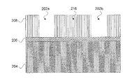
- プラズマ処理チャンバを含むプラズマ処理システムにおいて、基板の加工処理工程における処理の選択性を改善する方法であって、
処理ガス混合物と親和性を有するプレコートガス混合物を前記プラズマ処理チャンバ内に流入させる工程と、
前記プレコートガス混合物の第一プラズマを照射する工程と、
前記基板を前記プラズマ処理チャンバに導入する工程と、
前記プラズマ処理チャンバ内に処理ガス混合物を流入させる工程と、
前記処理ガス混合物の第二プラズマを照射する工程と、
前記第二プラズマにより前記基板をエッチングと積層の少なくとも1つを実施する工程と、
を含み、
前記第一プラズマが、前記プラズマ処理チャンバ内の表面にプレコート膜を形成して、前記第二プラズマ中の少なくともいくらかの量のラジカルを引きつけるように構成されており、
前記プレコートガス混合物が、CH2F2とCF4との混合物で構成されており、
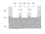
前記プレコートガス混合物を流入させる前に、ウエハのない状態で前記プラズマ処理チャンバを清浄化する工程を有していることを特徴とする処理の選択性を改善する方法。 - 前記処理ガス混合物が、エッチング種を含んでおり、
前記プレコート膜が、保護膜形成種を形成するために前記エッチング種と化学的に反応し、
前記保護膜形成種が前記基板の少なくとも一部を被覆する請求項1記載の方法。 - 前記処理の選択性が、フォトレジストのエッチングの選択性である請求項1記載の方法。
- 前記処理の選択性が、BARCのエッチングの選択性である請求項1記載の方法。
- 前記処理の選択性が、無機材料のエッチングの選択性である請求項1記載の方法。
- 前記処理の選択性が、シリコンのエッチングの選択性である請求項1記載の方法。
Applications Claiming Priority (3)
| Application Number | Priority Date | Filing Date | Title |
|---|---|---|---|
| US10/883,282 | 2004-06-30 | ||
| US10/883,282 US7316785B2 (en) | 2004-06-30 | 2004-06-30 | Methods and apparatus for the optimization of etch resistance in a plasma processing system |
| PCT/US2005/021047 WO2006011996A2 (en) | 2004-06-30 | 2005-06-14 | Methods and apparatus for the optimization of etch resistance in a plasma processing system |
Related Child Applications (1)
| Application Number | Title | Priority Date | Filing Date |
|---|---|---|---|
| JP2012199346A Division JP5567084B2 (ja) | 2004-06-30 | 2012-09-11 | プラズマ処理システムにおけるエッチング耐性を最適にする方法 |
Publications (3)
| Publication Number | Publication Date |
|---|---|
| JP2008505490A JP2008505490A (ja) | 2008-02-21 |
| JP2008505490A5 JP2008505490A5 (ja) | 2008-07-03 |
| JP5139059B2 true JP5139059B2 (ja) | 2013-02-06 |
Family
ID=35512818
Family Applications (2)
| Application Number | Title | Priority Date | Filing Date |
|---|---|---|---|
| JP2007519252A Active JP5139059B2 (ja) | 2004-06-30 | 2005-06-14 | プラズマ処理システムにおけるエッチング耐性を最適にする方法 |
| JP2012199346A Active JP5567084B2 (ja) | 2004-06-30 | 2012-09-11 | プラズマ処理システムにおけるエッチング耐性を最適にする方法 |
Family Applications After (1)
| Application Number | Title | Priority Date | Filing Date |
|---|---|---|---|
| JP2012199346A Active JP5567084B2 (ja) | 2004-06-30 | 2012-09-11 | プラズマ処理システムにおけるエッチング耐性を最適にする方法 |
Country Status (6)
| Country | Link |
|---|---|
| US (1) | US7316785B2 (ja) |
| JP (2) | JP5139059B2 (ja) |
| KR (1) | KR101233453B1 (ja) |
| CN (1) | CN101263092A (ja) |
| TW (1) | TWI389196B (ja) |
| WO (1) | WO2006011996A2 (ja) |
Families Citing this family (15)
| Publication number | Priority date | Publication date | Assignee | Title |
|---|---|---|---|---|
| US8546264B2 (en) * | 2005-06-02 | 2013-10-01 | The Regents Of The University Of California | Etching radical controlled gas chopped deep reactive ion etching |
| US7906032B2 (en) * | 2006-03-31 | 2011-03-15 | Tokyo Electron Limited | Method for conditioning a process chamber |
| US8501627B2 (en) * | 2007-09-27 | 2013-08-06 | Lam Research Corporation | Profile control in dielectric etch |
| US8298958B2 (en) | 2008-07-17 | 2012-10-30 | Lam Research Corporation | Organic line width roughness with H2 plasma treatment |
| CN101930921B (zh) * | 2009-06-25 | 2012-09-26 | 中芯国际集成电路制造(上海)有限公司 | 提高栅极尺寸均匀性的方法 |
| JP5450187B2 (ja) * | 2010-03-16 | 2014-03-26 | 株式会社日立ハイテクノロジーズ | プラズマ処理装置およびプラズマ処理方法 |
| JP2012015343A (ja) * | 2010-07-01 | 2012-01-19 | Hitachi High-Technologies Corp | プラズマエッチング方法 |
| TWI458011B (zh) * | 2010-10-29 | 2014-10-21 | Macronix Int Co Ltd | 蝕刻多層硬式幕罩的方法 |
| US8420947B2 (en) | 2010-12-30 | 2013-04-16 | Globalfoundries Singapore Pte. Ltd. | Integrated circuit system with ultra-low k dielectric and method of manufacture thereof |
| JP5956933B2 (ja) | 2013-01-15 | 2016-07-27 | 東京エレクトロン株式会社 | プラズマ処理方法及びプラズマ処理装置 |
| US9412606B2 (en) * | 2014-02-14 | 2016-08-09 | Taiwan Semiconductor Manufacturing Company Limited | Target dimension uniformity for semiconductor wafers |
| JP6169666B2 (ja) * | 2015-10-20 | 2017-07-26 | 株式会社日立ハイテクノロジーズ | プラズマ処理方法 |
| JP6568457B2 (ja) * | 2015-11-11 | 2019-08-28 | 株式会社日立ハイテクノロジーズ | プラズマ処理方法 |
| US9941123B1 (en) * | 2017-04-10 | 2018-04-10 | Lam Research Corporation | Post etch treatment to prevent pattern collapse |
| WO2019138654A1 (ja) * | 2018-10-26 | 2019-07-18 | 株式会社日立ハイテクノロジーズ | プラズマ処理装置及びプラズマ処理方法 |
Family Cites Families (22)
| Publication number | Priority date | Publication date | Assignee | Title |
|---|---|---|---|---|
| EP0394597A1 (en) * | 1989-04-28 | 1990-10-31 | International Business Machines Corporation | Follow-up System for Monitoring the Etching Process in an RIE Equipment and its Application to Producing High-resolution and Reproducible Patterns |
| JPH0828348B2 (ja) * | 1991-02-07 | 1996-03-21 | ヤマハ株式会社 | ドライエッチング方法 |
| JPH04313223A (ja) * | 1991-04-04 | 1992-11-05 | Mitsubishi Electric Corp | 半導体装置の製造方法 |
| US5482749A (en) * | 1993-06-28 | 1996-01-09 | Applied Materials, Inc. | Pretreatment process for treating aluminum-bearing surfaces of deposition chamber prior to deposition of tungsten silicide coating on substrate therein |
| US5571576A (en) * | 1995-02-10 | 1996-11-05 | Watkins-Johnson | Method of forming a fluorinated silicon oxide layer using plasma chemical vapor deposition |
| JP3067576B2 (ja) * | 1995-03-17 | 2000-07-17 | 株式会社日立製作所 | プラズマエッチング方法 |
| US5647953A (en) * | 1995-12-22 | 1997-07-15 | Lam Research Corporation | Plasma cleaning method for removing residues in a plasma process chamber |
| US6071573A (en) * | 1997-12-30 | 2000-06-06 | Lam Research Corporation | Process for precoating plasma CVD reactors |
| TW440952B (en) * | 1999-07-12 | 2001-06-16 | Lam Res Co Ltd | Waferless clean process of dry etcher |
| US6274500B1 (en) * | 1999-10-12 | 2001-08-14 | Chartered Semiconductor Manufacturing Ltd. | Single wafer in-situ dry clean and seasoning for plasma etching process |
| US6451703B1 (en) * | 2000-03-10 | 2002-09-17 | Applied Materials, Inc. | Magnetically enhanced plasma etch process using a heavy fluorocarbon etching gas |
| US6420274B1 (en) * | 2000-05-10 | 2002-07-16 | International Business Machines Corporation | Method for conditioning process chambers |
| JP2002025977A (ja) * | 2000-07-06 | 2002-01-25 | Hitachi Ltd | ドライエッチング方法 |
| JP2002184754A (ja) * | 2000-12-13 | 2002-06-28 | Seiko Epson Corp | ドライエッチング装置のシーズニング方法 |
| US6626187B2 (en) * | 2001-02-07 | 2003-09-30 | Promos Technologies Inc. | Method of reconditioning reaction chamber |
| US6455333B1 (en) * | 2001-02-28 | 2002-09-24 | Advanced Micro Devices, Inc. | Method of achieving stable deep ultraviolet (DUV) resist etch rate for gate critical dimension (CD) |
| JP2002270584A (ja) * | 2001-03-08 | 2002-09-20 | Toshiba Corp | 半導体装置の製造方法 |
| JP2002319571A (ja) * | 2001-04-20 | 2002-10-31 | Kawasaki Microelectronics Kk | エッチング槽の前処理方法及び半導体装置の製造方法 |
| JP4322484B2 (ja) * | 2002-08-30 | 2009-09-02 | 東京エレクトロン株式会社 | プラズマ処理方法及びプラズマ処理装置 |
| JP4034164B2 (ja) * | 2002-10-28 | 2008-01-16 | 富士通株式会社 | 微細パターンの作製方法及び半導体装置の製造方法 |
| US20040110388A1 (en) * | 2002-12-06 | 2004-06-10 | International Business Machines Corporation | Apparatus and method for shielding a wafer from charged particles during plasma etching |
| US6869542B2 (en) * | 2003-03-12 | 2005-03-22 | International Business Machines Corporation | Hard mask integrated etch process for patterning of silicon oxide and other dielectric materials |
-
2004
- 2004-06-30 US US10/883,282 patent/US7316785B2/en active Active
-
2005
- 2005-06-14 JP JP2007519252A patent/JP5139059B2/ja active Active
- 2005-06-14 KR KR1020077002286A patent/KR101233453B1/ko active IP Right Grant
- 2005-06-14 WO PCT/US2005/021047 patent/WO2006011996A2/en active Application Filing
- 2005-06-14 CN CNA2005800276665A patent/CN101263092A/zh active Pending
- 2005-06-29 TW TW094121944A patent/TWI389196B/zh active
-
2012
- 2012-09-11 JP JP2012199346A patent/JP5567084B2/ja active Active
Also Published As
| Publication number | Publication date |
|---|---|
| KR20070033010A (ko) | 2007-03-23 |
| JP5567084B2 (ja) | 2014-08-06 |
| TWI389196B (zh) | 2013-03-11 |
| JP2008505490A (ja) | 2008-02-21 |
| US7316785B2 (en) | 2008-01-08 |
| TW200614369A (en) | 2006-05-01 |
| US20060000797A1 (en) | 2006-01-05 |
| CN101263092A (zh) | 2008-09-10 |
| JP2012253386A (ja) | 2012-12-20 |
| WO2006011996A2 (en) | 2006-02-02 |
| WO2006011996A3 (en) | 2007-04-19 |
| KR101233453B1 (ko) | 2013-02-14 |
Similar Documents
| Publication | Publication Date | Title |
|---|---|---|
| JP5567084B2 (ja) | プラズマ処理システムにおけるエッチング耐性を最適にする方法 | |
| US6074959A (en) | Method manifesting a wide process window and using hexafluoropropane or other hydrofluoropropanes to selectively etch oxide | |
| US6183655B1 (en) | Tunable process for selectively etching oxide using fluoropropylene and a hydrofluorocarbon | |
| US6291357B1 (en) | Method and apparatus for etching a substrate with reduced microloading | |
| JP5492557B2 (ja) | 半導体基板を均一にエッチングするためのガス噴射 | |
| US8809199B2 (en) | Method of etching features in silicon nitride films | |
| US6569774B1 (en) | Method to eliminate striations and surface roughness caused by dry etch | |
| US20180286707A1 (en) | Gas additives for sidewall passivation during high aspect ratio cryogenic etch | |
| US6541164B1 (en) | Method for etching an anti-reflective coating | |
| US7186661B2 (en) | Method to improve profile control and N/P loading in dual doped gate applications | |
| US20130344702A1 (en) | Method of etching silicon nitride films | |
| KR20160075358A (ko) | 선택적인 질화물 에칭 | |
| US20060186087A1 (en) | Etchant and method of use | |
| KR20200027568A (ko) | 순환적 패시베이션 및 에칭을 사용한 고 종횡비 선택적 측방향 에칭 | |
| US20070298617A1 (en) | Processing method | |
| US20070119545A1 (en) | Method to improve profile control and n/p loading in dual doped gate applications | |
| US7141505B2 (en) | Method for bilayer resist plasma etch | |
| US6410451B2 (en) | Techniques for improving etching in a plasma processing chamber | |
| US20030148224A1 (en) | Methods for controlling and reducing profile variation in photoresist trimming | |
| KR20150031227A (ko) | 플라즈마 에칭 방법 및 플라즈마 처리 장치 | |
| US20190362983A1 (en) | Systems and methods for etching oxide nitride stacks | |
| CN101133682A (zh) | 用于蚀刻具有受控制的制程结果分配的方法 | |
| US20050239290A1 (en) | Trench photolithography rework for removal of photoresist residue | |
| US20030153193A1 (en) | Etching method | |
| TW202405942A (zh) | 用於半導體製造的蝕刻方法 |
Legal Events
| Date | Code | Title | Description |
|---|---|---|---|
| A521 | Request for written amendment filed |
Free format text: JAPANESE INTERMEDIATE CODE: A523 Effective date: 20080514 |
|
| A621 | Written request for application examination |
Free format text: JAPANESE INTERMEDIATE CODE: A621 Effective date: 20080514 |
|
| A977 | Report on retrieval |
Free format text: JAPANESE INTERMEDIATE CODE: A971007 Effective date: 20110310 |
|
| A131 | Notification of reasons for refusal |
Free format text: JAPANESE INTERMEDIATE CODE: A131 Effective date: 20110315 |
|
| A601 | Written request for extension of time |
Free format text: JAPANESE INTERMEDIATE CODE: A601 Effective date: 20110614 |
|
| A602 | Written permission of extension of time |
Free format text: JAPANESE INTERMEDIATE CODE: A602 Effective date: 20110621 |
|
| A601 | Written request for extension of time |
Free format text: JAPANESE INTERMEDIATE CODE: A601 Effective date: 20110705 |
|
| A602 | Written permission of extension of time |
Free format text: JAPANESE INTERMEDIATE CODE: A602 Effective date: 20110712 |
|
| A601 | Written request for extension of time |
Free format text: JAPANESE INTERMEDIATE CODE: A601 Effective date: 20110812 |
|
| A602 | Written permission of extension of time |
Free format text: JAPANESE INTERMEDIATE CODE: A602 Effective date: 20110819 |
|
| A521 | Request for written amendment filed |
Free format text: JAPANESE INTERMEDIATE CODE: A523 Effective date: 20110825 |
|
| A131 | Notification of reasons for refusal |
Free format text: JAPANESE INTERMEDIATE CODE: A131 Effective date: 20111025 |
|
| A601 | Written request for extension of time |
Free format text: JAPANESE INTERMEDIATE CODE: A601 Effective date: 20120124 |
|
| A602 | Written permission of extension of time |
Free format text: JAPANESE INTERMEDIATE CODE: A602 Effective date: 20120131 |
|
| A601 | Written request for extension of time |
Free format text: JAPANESE INTERMEDIATE CODE: A601 Effective date: 20120221 |
|
| A602 | Written permission of extension of time |
Free format text: JAPANESE INTERMEDIATE CODE: A602 Effective date: 20120228 |
|
| A521 | Request for written amendment filed |
Free format text: JAPANESE INTERMEDIATE CODE: A523 Effective date: 20120321 |
|
| A02 | Decision of refusal |
Free format text: JAPANESE INTERMEDIATE CODE: A02 Effective date: 20120515 |
|
| A521 | Request for written amendment filed |
Free format text: JAPANESE INTERMEDIATE CODE: A523 Effective date: 20120911 |
|
| A521 | Request for written amendment filed |
Free format text: JAPANESE INTERMEDIATE CODE: A821 Effective date: 20120911 |
|
| A911 | Transfer to examiner for re-examination before appeal (zenchi) |
Free format text: JAPANESE INTERMEDIATE CODE: A911 Effective date: 20121003 |
|
| TRDD | Decision of grant or rejection written | ||
| A01 | Written decision to grant a patent or to grant a registration (utility model) |
Free format text: JAPANESE INTERMEDIATE CODE: A01 Effective date: 20121023 |
|
| A01 | Written decision to grant a patent or to grant a registration (utility model) |
Free format text: JAPANESE INTERMEDIATE CODE: A01 |
|
| A61 | First payment of annual fees (during grant procedure) |
Free format text: JAPANESE INTERMEDIATE CODE: A61 Effective date: 20121115 |
|
| R150 | Certificate of patent or registration of utility model |
Ref document number: 5139059 Country of ref document: JP Free format text: JAPANESE INTERMEDIATE CODE: R150 Free format text: JAPANESE INTERMEDIATE CODE: R150 |
|
| FPAY | Renewal fee payment (event date is renewal date of database) |
Free format text: PAYMENT UNTIL: 20151122 Year of fee payment: 3 |
|
| RD02 | Notification of acceptance of power of attorney |
Free format text: JAPANESE INTERMEDIATE CODE: R3D02 |
|
| R250 | Receipt of annual fees |
Free format text: JAPANESE INTERMEDIATE CODE: R250 |
|
| R250 | Receipt of annual fees |
Free format text: JAPANESE INTERMEDIATE CODE: R250 |
|
| R250 | Receipt of annual fees |
Free format text: JAPANESE INTERMEDIATE CODE: R250 |
|
| R250 | Receipt of annual fees |
Free format text: JAPANESE INTERMEDIATE CODE: R250 |
|
| R250 | Receipt of annual fees |
Free format text: JAPANESE INTERMEDIATE CODE: R250 |
|
| R250 | Receipt of annual fees |
Free format text: JAPANESE INTERMEDIATE CODE: R250 |
|
| R250 | Receipt of annual fees |
Free format text: JAPANESE INTERMEDIATE CODE: R250 |
|
| R250 | Receipt of annual fees |
Free format text: JAPANESE INTERMEDIATE CODE: R250 |
|
| R250 | Receipt of annual fees |
Free format text: JAPANESE INTERMEDIATE CODE: R250 |