JP5139059B2 - Method for optimizing etch resistance in plasma processing systems - Google Patents
Method for optimizing etch resistance in plasma processing systems Download PDFInfo
- Publication number
- JP5139059B2 JP5139059B2 JP2007519252A JP2007519252A JP5139059B2 JP 5139059 B2 JP5139059 B2 JP 5139059B2 JP 2007519252 A JP2007519252 A JP 2007519252A JP 2007519252 A JP2007519252 A JP 2007519252A JP 5139059 B2 JP5139059 B2 JP 5139059B2
- Authority
- JP
- Japan
- Prior art keywords
- plasma processing
- plasma
- etching
- substrate
- photoresist
- Prior art date
- Legal status (The legal status is an assumption and is not a legal conclusion. Google has not performed a legal analysis and makes no representation as to the accuracy of the status listed.)
- Active
Links
- 238000000034 method Methods 0.000 title claims description 82
- 238000012545 processing Methods 0.000 title claims description 69
- 238000005530 etching Methods 0.000 claims description 60
- 239000000758 substrate Substances 0.000 claims description 60
- 229920002120 photoresistant polymer Polymers 0.000 claims description 55
- 230000008569 process Effects 0.000 claims description 49
- 239000000203 mixture Substances 0.000 claims description 21
- XUIMIQQOPSSXEZ-UHFFFAOYSA-N Silicon Chemical compound [Si] XUIMIQQOPSSXEZ-UHFFFAOYSA-N 0.000 claims description 4
- 238000004140 cleaning Methods 0.000 claims description 4
- 230000001678 irradiating effect Effects 0.000 claims description 4
- 230000001681 protective effect Effects 0.000 claims description 4
- 229910052710 silicon Inorganic materials 0.000 claims description 4
- 239000010703 silicon Substances 0.000 claims description 4
- 229910010272 inorganic material Inorganic materials 0.000 claims description 2
- 239000011147 inorganic material Substances 0.000 claims description 2
- 239000010410 layer Substances 0.000 description 46
- 239000007789 gas Substances 0.000 description 33
- 239000004065 semiconductor Substances 0.000 description 21
- 238000000576 coating method Methods 0.000 description 10
- 229910052734 helium Inorganic materials 0.000 description 10
- 239000000460 chlorine Substances 0.000 description 8
- 229910021420 polycrystalline silicon Inorganic materials 0.000 description 8
- 229920005591 polysilicon Polymers 0.000 description 8
- 230000000873 masking effect Effects 0.000 description 7
- 229910052757 nitrogen Inorganic materials 0.000 description 7
- 239000001301 oxygen Substances 0.000 description 6
- 229910052760 oxygen Inorganic materials 0.000 description 6
- 239000011248 coating agent Substances 0.000 description 5
- 239000000463 material Substances 0.000 description 5
- 229910003902 SiCl 4 Inorganic materials 0.000 description 4
- QVGXLLKOCUKJST-UHFFFAOYSA-N atomic oxygen Chemical compound [O] QVGXLLKOCUKJST-UHFFFAOYSA-N 0.000 description 4
- 238000001816 cooling Methods 0.000 description 4
- 238000006243 chemical reaction Methods 0.000 description 3
- 238000009792 diffusion process Methods 0.000 description 3
- 239000011521 glass Substances 0.000 description 3
- 239000001307 helium Substances 0.000 description 3
- SWQJXJOGLNCZEY-UHFFFAOYSA-N helium atom Chemical compound [He] SWQJXJOGLNCZEY-UHFFFAOYSA-N 0.000 description 3
- 238000002513 implantation Methods 0.000 description 3
- 230000006698 induction Effects 0.000 description 3
- 238000004519 manufacturing process Methods 0.000 description 3
- 238000009832 plasma treatment Methods 0.000 description 3
- 229920000642 polymer Polymers 0.000 description 3
- 239000011241 protective layer Substances 0.000 description 3
- VYPSYNLAJGMNEJ-UHFFFAOYSA-N Silicium dioxide Chemical compound O=[Si]=O VYPSYNLAJGMNEJ-UHFFFAOYSA-N 0.000 description 2
- 230000015572 biosynthetic process Effects 0.000 description 2
- 238000000151 deposition Methods 0.000 description 2
- 230000008021 deposition Effects 0.000 description 2
- 238000010586 diagram Methods 0.000 description 2
- 238000009826 distribution Methods 0.000 description 2
- 230000000694 effects Effects 0.000 description 2
- 230000010354 integration Effects 0.000 description 2
- 229910052751 metal Inorganic materials 0.000 description 2
- 239000002184 metal Substances 0.000 description 2
- 150000004767 nitrides Chemical class 0.000 description 2
- 238000001020 plasma etching Methods 0.000 description 2
- 230000002829 reductive effect Effects 0.000 description 2
- 239000000126 substance Substances 0.000 description 2
- 238000004381 surface treatment Methods 0.000 description 2
- ZOXJGFHDIHLPTG-UHFFFAOYSA-N Boron Chemical compound [B] ZOXJGFHDIHLPTG-UHFFFAOYSA-N 0.000 description 1
- ZAMOUSCENKQFHK-UHFFFAOYSA-N Chlorine atom Chemical compound [Cl] ZAMOUSCENKQFHK-UHFFFAOYSA-N 0.000 description 1
- VYZAMTAEIAYCRO-UHFFFAOYSA-N Chromium Chemical compound [Cr] VYZAMTAEIAYCRO-UHFFFAOYSA-N 0.000 description 1
- 241001634884 Cochlicopa lubricella Species 0.000 description 1
- UFHFLCQGNIYNRP-UHFFFAOYSA-N Hydrogen Chemical compound [H][H] UFHFLCQGNIYNRP-UHFFFAOYSA-N 0.000 description 1
- OAICVXFJPJFONN-UHFFFAOYSA-N Phosphorus Chemical compound [P] OAICVXFJPJFONN-UHFFFAOYSA-N 0.000 description 1
- 239000000654 additive Substances 0.000 description 1
- 230000000996 additive effect Effects 0.000 description 1
- 239000000443 aerosol Substances 0.000 description 1
- 230000004075 alteration Effects 0.000 description 1
- 229910021417 amorphous silicon Inorganic materials 0.000 description 1
- 230000004888 barrier function Effects 0.000 description 1
- 238000005452 bending Methods 0.000 description 1
- 230000000903 blocking effect Effects 0.000 description 1
- 229910052796 boron Inorganic materials 0.000 description 1
- 229910052799 carbon Inorganic materials 0.000 description 1
- 239000003795 chemical substances by application Substances 0.000 description 1
- 238000005229 chemical vapour deposition Methods 0.000 description 1
- 229910052801 chlorine Inorganic materials 0.000 description 1
- 229910052804 chromium Inorganic materials 0.000 description 1
- 239000011651 chromium Substances 0.000 description 1
- 230000003750 conditioning effect Effects 0.000 description 1
- -1 contains H 2 Inorganic materials 0.000 description 1
- 238000011109 contamination Methods 0.000 description 1
- 239000002826 coolant Substances 0.000 description 1
- 230000003247 decreasing effect Effects 0.000 description 1
- 230000007547 defect Effects 0.000 description 1
- 238000007599 discharging Methods 0.000 description 1
- 239000006185 dispersion Substances 0.000 description 1
- 238000005108 dry cleaning Methods 0.000 description 1
- 239000000839 emulsion Substances 0.000 description 1
- 238000005516 engineering process Methods 0.000 description 1
- 230000003628 erosive effect Effects 0.000 description 1
- 239000012634 fragment Substances 0.000 description 1
- 230000001788 irregular Effects 0.000 description 1
- 238000012423 maintenance Methods 0.000 description 1
- 230000007246 mechanism Effects 0.000 description 1
- 239000011859 microparticle Substances 0.000 description 1
- 238000012986 modification Methods 0.000 description 1
- 230000004048 modification Effects 0.000 description 1
- IJGRMHOSHXDMSA-UHFFFAOYSA-N nitrogen Substances N#N IJGRMHOSHXDMSA-UHFFFAOYSA-N 0.000 description 1
- QJGQUHMNIGDVPM-UHFFFAOYSA-N nitrogen(.) Chemical compound [N] QJGQUHMNIGDVPM-UHFFFAOYSA-N 0.000 description 1
- NJPPVKZQTLUDBO-UHFFFAOYSA-N novaluron Chemical compound C1=C(Cl)C(OC(F)(F)C(OC(F)(F)F)F)=CC=C1NC(=O)NC(=O)C1=C(F)C=CC=C1F NJPPVKZQTLUDBO-UHFFFAOYSA-N 0.000 description 1
- 238000005457 optimization Methods 0.000 description 1
- 230000003647 oxidation Effects 0.000 description 1
- 238000007254 oxidation reaction Methods 0.000 description 1
- 230000036961 partial effect Effects 0.000 description 1
- 239000002245 particle Substances 0.000 description 1
- 229910052698 phosphorus Inorganic materials 0.000 description 1
- 239000011574 phosphorus Substances 0.000 description 1
- 230000003449 preventive effect Effects 0.000 description 1
- 238000005086 pumping Methods 0.000 description 1
- 238000011160 research Methods 0.000 description 1
- 238000007789 sealing Methods 0.000 description 1
- 235000012239 silicon dioxide Nutrition 0.000 description 1
- 239000000377 silicon dioxide Substances 0.000 description 1
- 125000006850 spacer group Chemical group 0.000 description 1
- 230000006641 stabilisation Effects 0.000 description 1
- 238000011105 stabilization Methods 0.000 description 1
- 230000000087 stabilizing effect Effects 0.000 description 1
- 238000006467 substitution reaction Methods 0.000 description 1
- 238000012546 transfer Methods 0.000 description 1
Images


Classifications
-
- H—ELECTRICITY
- H01—ELECTRIC ELEMENTS
- H01J—ELECTRIC DISCHARGE TUBES OR DISCHARGE LAMPS
- H01J37/00—Discharge tubes with provision for introducing objects or material to be exposed to the discharge, e.g. for the purpose of examination or processing thereof
- H01J37/32—Gas-filled discharge tubes
- H01J37/32431—Constructional details of the reactor
- H01J37/32798—Further details of plasma apparatus not provided for in groups H01J37/3244 - H01J37/32788; special provisions for cleaning or maintenance of the apparatus
- H01J37/32853—Hygiene
- H01J37/32862—In situ cleaning of vessels and/or internal parts
-
- H—ELECTRICITY
- H01—ELECTRIC ELEMENTS
- H01L—SEMICONDUCTOR DEVICES NOT COVERED BY CLASS H10
- H01L21/00—Processes or apparatus adapted for the manufacture or treatment of semiconductor or solid state devices or of parts thereof
- H01L21/02—Manufacture or treatment of semiconductor devices or of parts thereof
- H01L21/04—Manufacture or treatment of semiconductor devices or of parts thereof the devices having at least one potential-jump barrier or surface barrier, e.g. PN junction, depletion layer or carrier concentration layer
- H01L21/18—Manufacture or treatment of semiconductor devices or of parts thereof the devices having at least one potential-jump barrier or surface barrier, e.g. PN junction, depletion layer or carrier concentration layer the devices having semiconductor bodies comprising elements of Group IV of the Periodic System or AIIIBV compounds with or without impurities, e.g. doping materials
- H01L21/30—Treatment of semiconductor bodies using processes or apparatus not provided for in groups H01L21/20 - H01L21/26
- H01L21/302—Treatment of semiconductor bodies using processes or apparatus not provided for in groups H01L21/20 - H01L21/26 to change their surface-physical characteristics or shape, e.g. etching, polishing, cutting
- H01L21/306—Chemical or electrical treatment, e.g. electrolytic etching
- H01L21/3065—Plasma etching; Reactive-ion etching
-
- H—ELECTRICITY
- H01—ELECTRIC ELEMENTS
- H01J—ELECTRIC DISCHARGE TUBES OR DISCHARGE LAMPS
- H01J37/00—Discharge tubes with provision for introducing objects or material to be exposed to the discharge, e.g. for the purpose of examination or processing thereof
- H01J37/32—Gas-filled discharge tubes
- H01J37/32009—Arrangements for generation of plasma specially adapted for examination or treatment of objects, e.g. plasma sources
- H01J37/32082—Radio frequency generated discharge
Description
本発明は基板製造技術、特にプラズマ処理システムにおけるエッチング耐性を最適にする方法および装置に関する。 The present invention relates to substrate manufacturing techniques, and more particularly to a method and apparatus for optimizing etch resistance in plasma processing systems.
基板、例えば半導体基板やフラットパネルディスプレイの製造に用いられるガラスパネルには、プラズマ処理が採用される。基板処理の一部として、例えば基板が複数のダイ(dies)または長方形のエリアに分割され、それらが集積回路を構成する。基板は、一連の処理工程において素材の一部が除去(エッチング)されまたは堆積(deposited)される。数ナノメートルのオーダーの限界寸法(critical dimension:CD)でトランジスタゲートを制御することが最優先であり、ターゲットゲートの長さがナノメートルずれるだけで、これらの装置の操作スピードに直接影響するからである。 Plasma processing is employed for glass panels used in the manufacture of substrates, such as semiconductor substrates and flat panel displays. As part of the substrate processing, for example, the substrate is divided into a plurality of dies or rectangular areas, which constitute an integrated circuit. The substrate is partially removed (etched) or deposited in a series of processing steps. Controlling transistor gates with a critical dimension (CD) on the order of a few nanometers is a top priority, and only a nanometer shift in target gate length directly affects the operating speed of these devices. It is.
典型的なプラズマ処理における基板上へのゲートセットの形成では、化学気相成長法によりシリコン基板上にp型エピタキシャル層が配置される。エピタキシャル層の上に窒化物層が堆積し、特定のパターンにマスキングおよびエッチングがなされ、エピタキシャル層の上に除去されて露出された領域などを形成する(例えば、窒化物層で被覆されない領域)。これらの領域は、リンなどの添加物が拡散またはイオン注入される前に特定のパターンにマスクキングされ、nウェルを形成する。 In the formation of a gate set on a substrate in a typical plasma process, a p-type epitaxial layer is disposed on a silicon substrate by chemical vapor deposition. A nitride layer is deposited over the epitaxial layer, and a specific pattern is masked and etched to form areas that are removed and exposed on the epitaxial layer (eg, areas not covered by the nitride layer). These regions are masked in a specific pattern before an additive such as phosphorus is diffused or ion implanted to form an n-well.
硬化エマルジョンの領域は選択的に除去され、基底層の構成要素が露出される。基板は、モノポーラ(mono-polar)まはバイポーラ(bi-polar)電極を含む支持構造の上で、チャックあるいは台座(pedestal)に固定されてプラズマ処理チャンバ内にセットされる。適当なエッチング源がチャンバ内に導入され、基板の処理面にプラズマが照射されてエッチング処理される。 The areas of the hardened emulsion are selectively removed, exposing the base layer components. The substrate is set in a plasma processing chamber, secured to a chuck or pedestal on a support structure that includes mono-polar or bi-polar electrodes. An appropriate etching source is introduced into the chamber, and the processing surface of the substrate is irradiated with plasma to be etched.
二酸化シリコンが成長して酸化物領域を形成し、回路の他のパーツからnウェルを絶縁する。別のマスキング/酸化処理が繰り返されてnウェル上にゲート酸化物層が成長し、pチャネルMOSトランジスタが形成される。このゲート酸化物層はこれらトランジスタのチャネルおよびゲートの間の絶縁層として働く。他のエピタキシャル領域を閾値電圧で調整しつつ、別途マスキング、拡散、注入などの処理によって、nチャネルトランジスタが形成される。 Silicon dioxide grows to form oxide regions and insulates the n-well from other parts of the circuit. Another masking / oxidation process is repeated to grow a gate oxide layer on the n-well and form a p-channel MOS transistor. This gate oxide layer serves as an insulating layer between the channel and gate of these transistors. An n-channel transistor is formed by separately processing such as masking, diffusion, and implantation while adjusting other epitaxial regions with the threshold voltage.
ウエハ上のポリシリコン層の堆積が行われ、続いて不要なポリシリコン層の除去の為のマスキング/エッチングが繰り返されて、pチャネルトランジスタのゲート酸化物の上にポリシリコンゲートが画定される。同時に、正確な位置における酸化物のエッチングによって、nウェルの上にソースとドレインのドライブイン(拡散)のための開口が形成される。 A polysilicon layer is deposited on the wafer, followed by repeated masking / etching to remove unwanted polysilicon layers to define a polysilicon gate over the gate oxide of the p-channel transistor. At the same time, an oxide etch at a precise location forms an opening for source and drain drive-in (diffusion) over the n-well.
別にマスキング/注入が繰り返され、nウェルの新しい開口内にボロンドープおよびドライブインが行われて、p型のソースとドレインが形成される。その後、マスキング/注入が繰り返されて、p型エピタキシャルの中に、nチャネルトランジスタのn型ソースとドレインが形成される。 Separately, masking / implantation is repeated and boron doping and drive-in are performed in the new opening of the n-well to form p-type source and drain. Thereafter, masking / implantation is repeated to form the n-type source and drain of the n-channel transistor in the p-type epitaxial.
しかし、基板上に高密度回路の要求が高くなると、サブミクロンのオーダーにおける高いアスペクト比を持ったヴィアコンタクトやトレンチを形成するには、現在のプラズマ処理の技術を用いてもなかなか困難なものであった。特に、ゲート深さがリソグラフィックの光の波長よりも小さい場合には当該深さのゲートを作成することは非常に困難である。一つの一般的な方法としては、化学的に優位なエッチング処理を用いて、フォトレジストマスクを削ることである。この方法では所望の結果(プレエッチングのCD)と比較して外形のCDが大きなマスクが形成される。底部基板のトレンチが縦方向(基板に対して垂直)にエッチングされ、フォトレジストが左右方向(基板に対して水平方向)にエッチングされあるいは削られて、最終的に所望のゲートCDが形成されるのである。 However, as the demand for high-density circuits on the substrate increases, it is very difficult to form via contacts and trenches with high aspect ratios on the order of submicrons, even using current plasma processing technology. there were. In particular, when the gate depth is smaller than the wavelength of the lithographic light, it is very difficult to produce a gate having the depth. One common method is to scrape the photoresist mask using a chemically dominant etching process. In this method, a mask having a larger outer shape CD than the desired result (pre-etched CD) is formed. The bottom substrate trench is etched in the vertical direction (perpendicular to the substrate) and the photoresist is etched or scraped in the left-right direction (horizontal direction with respect to the substrate) to finally form the desired gate CD. It is.
一般的に、フォトレジストはリソグラフィックプロセス(コントラスト、解像度、インライン粗さなど)、インテグレーション(積層化)プロセス(エッチング選択性、化学的安定性、アッシング(ash)選択性など)ともに最適のものでなければならない。このようなタイプのフォトレジストは、化学的に優位なエッチングなどによって、積層化について影響を受けやすく、これらは“ソフト”といわれることがある。 In general, photoresists are optimal for both lithographic processes (contrast, resolution, in-line roughness, etc.) and integration (stacking) processes (etch selectivity, chemical stability, ash selectivity, etc.). There must be. These types of photoresists are susceptible to stacking, such as by chemical-dominant etching, and are sometimes referred to as “soft”.
ソフトフォトレジストのCDの制御は、リソグラフィック環境におけるサブミクロン〜100nmの範囲では特に困難である。フォトレジストは、フォトレジストの柱が崩壊しないようにして十分に薄くなければならず、エッチング層の所望のエッチング選択性の為に十分な厚みを有していなければならない。しかし、フォトレジストの柱が幅に比較して高さが不均衡(例えば、高さ対幅の比が4以上)であると、エッチング処理が損傷を与え、基板の電気的・機能的特性が変わり、基板の性能および製品の良品率に直接影響を与えてしまう。 Control of the soft photoresist CD is particularly difficult in the submicron to 100 nm range in a lithographic environment. The photoresist must be thin enough so that the pillars of the photoresist do not collapse and have a sufficient thickness for the desired etch selectivity of the etching layer. However, if the photoresist pillars are imbalanced in height compared to the width (eg, the height to width ratio is 4 or more), the etching process will be damaged and the electrical and functional characteristics of the substrate will be reduced. This will directly affect the performance of the board and the yield rate of the product.
例えば、ソフトフォトレジストがエッチングされると、小刻みな波状パターンが形成され、溝ができたり、マイクロローディング(micro-loading)やランダムなエッチングストップの原因となってしまう。溝は普通の形状の中に不揃いな形状を作り、マスキングの領域を余分に露出させる。従って、基板から意図しないエッチング除去が起き、その結果ウエハの電気的・機能的特性が変えられてしまうのである。一つの影響として例えば、フォトレジストの柱面の粗さが増加することもある。もし、フォトレジストの小刻みな波状パターンが集中したとすると、その結果マスキングパターンが、部分的あるいは完全に、所定の基材の除去をブロックしてしまう。 For example, when a soft photoresist is etched, a small wavy pattern is formed, resulting in grooves, micro-loading, and random etching stop. The groove creates an irregular shape in the normal shape and exposes the masking area. Therefore, unintended etching removal from the substrate occurs, and as a result, the electrical and functional characteristics of the wafer are changed. As one influence, for example, the roughness of the column surface of the photoresist may increase. If a small wavy pattern of photoresist is concentrated, the masking pattern results in partial or complete blocking of the removal of a given substrate.
トレンチフロアに基材が残ると、マイクロローディングが起こり、物理的に平らでない底部表面が形成されてしまう。エッチング処理の間に、フォトレジストの柱の入口でエッチングガスが妨げられると、ランダムなエッチングストップが発生する。ある状況においては、フォトレジストの柱が、高さと薄さが不均衡(例えば、高さ対幅の比が4以上)であると、フォトレジストの柱の全部が誤って除去あるいは剥がされてしまう。さらに横からのエッチング速度と縦からのエッチング速度が違う場合に、不均一なストレスにより、フォトレジストの柱が、よじれたり、曲げられたり、捻じられたりする。 If the substrate remains on the trench floor, microloading occurs and a bottom surface that is not physically flat is formed. During the etching process, if the etching gas is blocked at the photoresist column entrance, a random etch stop occurs. In some situations, if the photoresist pillars are imbalanced in height and thickness (eg, a height to width ratio of 4 or greater), all of the photoresist pillars may be accidentally removed or stripped. . Furthermore, when the etching rate from the side is different from the etching rate from the vertical, the pillars of the photoresist are kinked, bent, or twisted due to non-uniform stress.
図1を参照すると、プラズマ処理システムの構成が簡易的に表されている。一般に、適切なガス混合物がガス分散システム122から入力管108を通ってチャンバ102内へ流される。静電的チャック116の上にエッジリング115によって固定された半導体基板やガラス板材などの基板114の露出された領域を、表面処理(例えばエッチングや堆積など)するために、これらのプラズマ処理ガスはプラズマ110を形成するようにイオン化される。加えて、ライナー117はプラズマとプラズマ処理チャンバの間の熱バリアとしてだけでなく基板114上のプラズマ110の最適化に寄与する。
Referring to FIG. 1, the configuration of the plasma processing system is simply shown. In general, a suitable gas mixture is flowed from the
ガス分散システム122は、プラズマ処理ガス(例えば、C4F8、C4F6、CHF3、CH2F3、CF4、HBr、CH3F、C2F4、N2、O2、Ar、Xe、He、H2、NH3、SF6、BCl3、Cl2、WF6、その他)を含む圧縮ガスシリンダ124a−fを含んでいる。圧縮ガスシリンダ124a−fは、それぞれのガスを排出する機構を備えた容器128の中に保護されている。流速コントローラ126a−fは、(トランスデューサ、コントロールバルブ、信号処理エレクトロニクスなどを含む)自己調整型装置であり、半導体産業においてプラズマ処理システムへガス流量を測定し、調整するために用いられる。インジェクタ109は、チャンバ102内にエアロゾルとしてプラズマ処理ガス124を導入する。
The
誘導コイル131は絶縁ウィンドウ104によってプラズマから分離され、プラズマ110を生成するためにプラズマ処理ガス内に時変電流を誘導する。ウィンドウは誘導コイルをプラズマ110から保護し、プラズマ処理チャンバ内に発生された高周波(RF)フィールドを透過させる。さらに誘導コイル131はリード線130a−bによってマッチングネットワーク132と結合し、そして高周波発生器138とも結合している。マッチングネットワーク132は、高周波発生器138のインピーダンスをマッチングさせ、約13.56MHz、50オームで操作されて、プラズマ110に適用する。
一般に、冷却システムのあるタイプでは、プラズマの点火による熱平衡を保つためにチャックと結合している。冷却システム自身は、チャックの中の空間にクーラント(coolant)をポンピングするため冷却装置を含み、チャックと基板の間にヘリウムガスを送り込む。発生した熱を除去し、熱の拡散を素早くコントロールするために、ヘリウムガスが冷却システムとして用いられる。従って、ヘリウムの圧力が増加すると熱の移動速度も増大する。ほとんどのプラズマ処理システムは、操作ソフトウエアプログラムを有する複雑なコンピュータにより制御される。典型的操作環境において、製造プロセスパラメータ(例えば、電圧、ガス混合流量、ガス流速、圧力など)は特別なプラズマ処理システム及び具体的な方法により決定される。 In general, some types of cooling systems are coupled to a chuck to maintain thermal equilibrium due to plasma ignition. The cooling system itself includes a cooling device for pumping a coolant into the space in the chuck and pumps helium gas between the chuck and the substrate. Helium gas is used as a cooling system to remove the generated heat and to quickly control the diffusion of heat. Therefore, the heat transfer rate increases as the helium pressure increases. Most plasma processing systems are controlled by a complex computer having an operating software program. In a typical operating environment, manufacturing process parameters (eg, voltage, gas mix flow rate, gas flow rate, pressure, etc.) are determined by a special plasma processing system and specific method.
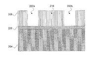
図2A−Bを参照すると、プラズマ処理により製造されたゲートの層構造断面図が示されている。図2Aは、リソグラフィック工程に先立つ、半導体ICの層構造を表す断面図である。以下の説明において“上”、“下”の用語は、層間の空間的な関係を意味し、層間の直接的な接続をも意味するものではない。他の付加的な層が上、下、または間に存在することに注意すべきである。さらに、存在する全ての層を表すものでもなく、他の異なる層によって構成されている場合もある。 Referring to FIGS. 2A-B, a cross-sectional view of the layer structure of a gate manufactured by plasma processing is shown. FIG. 2A is a cross-sectional view illustrating a layer structure of a semiconductor IC prior to a lithographic process. In the following description, the terms “upper” and “lower” mean a spatial relationship between layers, and do not mean a direct connection between layers. Note that other additional layers are present above, below, or between. Furthermore, it does not represent all the layers present but may be constituted by other different layers.
積層の底部は、図では層204として示されているが、ポリシリコンのような半導体を含んでいる。層204の上には、リソグラフィック処理を経たフォトレジストマスク層208とBARC層206が配置されている。この例では、フォトレジストマスクパターン216が最初にリソグラフィックによって形成され、トレンチゲート202a−bを形成するために化学的トリム(trimmed)が行われた後の状態を示している。
The bottom of the stack, shown in the figure as
図2Bは、トレンチゲート202a−bをさらに延長させるために、プラズマ処理システムによって層204がエッチングされた後の断面図を表している。さらに、フォトレジストマスク層が領域210の分、および基底半導体層204も横方向にエッチングされた状態を示す。
FIG. 2B shows a cross-sectional view after
図3A−Cを参照すると、プラズマ処理の間に崩壊されたソフトフォトレジストの柱を有する基板の断面を示している。エッチング処理によって、フォトレジスト材が横方向(基板に対して平行方向)、或いは縦方向(基板に対して垂直方向)に除去された状態である。もし柱の幅が十分に最小化されると、横方向と縦方向のエッチングの組合せが斜め方向に働いて、柱の大部分を除去してしまい、基底部の基板にも損傷を与える。 Referring to FIGS. 3A-C, a cross section of a substrate with soft photoresist pillars collapsed during plasma processing is shown. This is a state in which the photoresist material is removed in the lateral direction (a direction parallel to the substrate) or in the longitudinal direction (a direction perpendicular to the substrate) by the etching process. If the pillar width is sufficiently minimized, the combination of lateral and longitudinal etching acts diagonally, removing most of the pillars and damaging the base substrate.
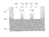
図3Aは、リソグラフィック工程に先立つ、典型的な半導体ICの断面図を表している。基底層は層304で示されており、ポリシリコンなどの半導体である。層304の上には、リソグラフィック処理後のフォトレジストマスク層308とBARC層306が形成されている。この例ではフォトレジストマスクパターンがトレンチ302a−cにゲートを形成するために、処理されている。
FIG. 3A shows a cross-sectional view of a typical semiconductor IC prior to the lithographic process. The base layer is indicated by
図3Bは、プラズマ処理システムによってフォトレジスト層308がエッチングされた後の断面を示している。しかし、これは図2A−Bに示す柱とは異なり、細い柱316が、エッチング処理により損傷を受けて柱312になっている。幅だけでなく、高さまでも壊滅的に減少している。
FIG. 3B shows a cross-section after the
図3Cは、図3Bの積層を、プラズマ処理システムによって層304をエッチングした後の断面図を示している。基底層304には大きな空間320が形成されてしまっている。
FIG. 3C shows a cross-sectional view of the stack of FIG. 3B after etching
図4A−Cを参照すると、不均一なソフトフォトレジストの柱がプラズマ処理の間に捻じられた状態を示す断面図である。前記の通り、フォトレジスト材が横方向(基板に対して平行方向)、或いは縦方向(基板に対して垂直方向)に除去された状態である。もし柱の幅が十分に最小化されると、横方向と縦方向のエッチングの組合せが、曲げられたり捻じられたりするストレスを生じさせる。 Referring to FIGS. 4A-C, cross-sectional views showing a non-uniform soft photoresist column twisted during plasma processing. As described above, the photoresist material is removed in the horizontal direction (parallel to the substrate) or in the vertical direction (perpendicular to the substrate). If the column width is sufficiently minimized, the combination of lateral and longitudinal etching creates stresses that can be bent or twisted.
図4Aは、リソグラフィック工程に先立つ、典型的な半導体ICの断面図を表している。積層の底には、ポリシリコンなどの半導体よりなる層404が示されている。層404の上には、リソグラフィック工程を経てフォトレジストマスク層408とBARC層406が形成されている。この例ではフォトレジストマスクパターンがトレンチゲート402a−cの形成のために、処理されている。
FIG. 4A shows a cross-sectional view of a typical semiconductor IC prior to a lithographic process. At the bottom of the stack, a
図4Bは図4Aの積層のフォトレジスト層408が、プラズマ処理システムによってエッチングされた後の断面図を示している。図2A−Bの柱216とは異なり、柱416がエッチング処理によって捻じられて柱412へ、また基底層404には非直線的な側壁面が形成されている。
FIG. 4B shows a cross-sectional view after the stacked
このように、プラズマ処理システムにおけるエッチング耐性を最適化する方法および装置が求められているのである。 Thus, there is a need for a method and apparatus that optimizes etch resistance in plasma processing systems.
本発明の具体例の一つは、プラズマ処理チャンバを含むプラズマ処理システムにおいて、基材のエッチングに対する耐性を最適化する方法に関する。該方法は、エッチングガス混合物と親和性を有するプレコート(pre-coat)ガス混合物をプラズマ処理チャンバに流入させる工程;プレコートガス混合物の第一プラズマを照射する工程;基材を含む基板を導入工程を含む。また、該方法は、プラズマ処理チャンバ内にエッチングガス混合物を流入させる工程;エッチングガス混合物の第二プラズマを照射する工程;第二プラズマにより基板をエッチングする工程;を含む。そして、プラズマ処理チャンバ内で、第一プラズマが露出表面にプレコート残留膜を形成し、基材のエッチング耐性が実質的に維持される。 One embodiment of the present invention relates to a method for optimizing substrate etch resistance in a plasma processing system including a plasma processing chamber. The method includes the steps of flowing a pre-coat gas mixture having an affinity for an etching gas mixture into a plasma processing chamber; irradiating a first plasma of the precoat gas mixture; introducing a substrate including a substrate; Including. The method also includes flowing an etching gas mixture into the plasma processing chamber; irradiating a second plasma of the etching gas mixture; etching the substrate with the second plasma. Then, in the plasma processing chamber, the first plasma forms a precoat residual film on the exposed surface, and the etching resistance of the substrate is substantially maintained.
本発明の特徴については、以下に図面を参照しつつ、さらに詳細に説明する。 The features of the present invention will be described in more detail below with reference to the drawings.
本発明について、いくつかの好ましい具体例とともに図面を参照しつつ更に詳細に説明する。以下の説明において、多くの詳細な説明は本発明を理解するために用いられる。当業者においては、これらの詳細な説明の一部または全部がなくても、本発明を実施することができるかもしれない。また、公知のプロセス、構造などについては、本発明を却って不明瞭にするかもしれないので詳細には記載していないことを理解すべきである。 The present invention will be described in more detail with reference to the drawings together with some preferred embodiments. In the following description, numerous detailed descriptions are used to understand the present invention. One skilled in the art may be able to practice the invention without some or all of these detailed descriptions. It should also be understood that well-known processes, structures, etc. are not described in detail because they may obscure the present invention.
前記の通り、深いゲートエッチングを、ソフトフォトレジスト(フォトレジストは集積化の問題による影響を受けやすい)を使用して得ることは困難である。特に、フォトレジストの柱の幅に比較して高さが不均衡(例えば、高さ対幅の比が4以上)であると、エッチング処理が該柱、そして後のゲート基材に損傷を与える。 As noted above, deep gate etching is difficult to obtain using soft photoresist (photoresist is susceptible to integration problems). In particular, if the height is unbalanced (eg, the height to width ratio is 4 or more) compared to the width of the photoresist pillar, the etching process will damage the pillar and the subsequent gate substrate. .
例えば、不均一なストレスがフォトレジストの柱によじれ、曲げ、捻じれ等を生じさせる原因となる。同様に、ファセット(facet)または非直線的な側面形状が該柱の壁に形成されて、基板の実質的な欠陥となる。ある状況においては、柱の高さ及び薄さが不均衡であると、フォトレジストの柱の全体が除去あるいは剥離され、さらには断面のCDや基板に対して損傷を与えることになる。伝統的な保護膜形成技術は一般的に役に立たない。何故なら、相対的な断面のCDは維持されるけれども、絶対的なサイズのCDは保護膜層を付加することにより増大するからである。 For example, non-uniform stress can cause kinking, bending, twisting, etc. of the photoresist pillars. Similarly, facets or non-linear side shapes are formed on the pillar walls, resulting in substantial defects in the substrate. In some situations, imbalance in column height and thinness can result in removal or stripping of the entire photoresist column and even damage to the cross-sectional CD and substrate. Traditional protective film formation techniques are generally useless. This is because the relative cross-section CD is maintained, but the absolute size CD is increased by adding a protective layer.
限定されることを望むものではないが、エッチング剤(例えばフォトレジストエッチング剤)と親和性(誘引性)のある材料でプラズマ処理チャンバをプレコートすることにより、基板が正確にエッチングされるだけでなく、エッチング剤の選択性を最適化できる。 While not wishing to be limited, pre-coating the plasma processing chamber with a material that is compatible (attractive) with an etchant (eg, a photoresist etchant) will not only accurately etch the substrate. The selectivity of the etching agent can be optimized.
一般に、プラズマ処理のエッチング工程の後、ドライクリーニング、ウエハの無い状態でのクリーニング、予防保守などにより反応チャンバの内表面に接着したミクロな粒子や残留ポリマを除去する。次の基板を入れる前に、エッチング剤と親和性のある材料でプラズマチャンバをプレコートすることによって、プラズマ中のエッチングラジカルの効果量が減少し、エッチング速度(例えば、フォトレジストの完全性を維持するためなど)が最適化される。 In general, after the plasma processing etching step, micro particles and residual polymer adhered to the inner surface of the reaction chamber are removed by dry cleaning, cleaning without a wafer, preventive maintenance, and the like. By precoating the plasma chamber with a material that is compatible with the etchant before the next substrate is loaded, the effective amount of etch radicals in the plasma is reduced and the etch rate (eg, maintaining the integrity of the photoresist). To optimize).
例えば、多くのフォトレジストエッチング剤は酸素を含んでいる。酸素と親和性のある塩素などでチャンバをプレコートすると、プラズマ中の酸素ラジカルの効果量が減少し、それがフォトレジストのエッチングには有効なのである。しかし、プレコート材の量が多すぎるとエッチング処理に有効な酸素ラジカルの数も殆どなくなってしまう。制御可能なポリマー保護層は、プレコートとフォトレジストエッチング剤との反応によって生成され、フォトレジストの完全性保護の為にエッチング処理を最適化する。ポリマー保護層はフォトレジストマスクの垂直方向と水平方向の浸食を防止し基板のCD維持にとって有効なのである。 For example, many photoresist etchants contain oxygen. Pre-coating the chamber with chlorine, which has an affinity for oxygen, reduces the effective amount of oxygen radicals in the plasma, which is effective for photoresist etching. However, if the amount of the precoat material is too large, the number of oxygen radicals effective for the etching process is almost eliminated. A controllable polymer protective layer is produced by the reaction of the precoat and the photoresist etchant, optimizing the etching process for photoresist integrity protection. The polymer protective layer prevents erosion in the vertical and horizontal directions of the photoresist mask and is effective for maintaining the CD of the substrate.
米国特許6455333号では、特有の積層を有するウエハをエッチングチャンバ内で処理して、深紫外線(deep ultraviolet:DUV)レジストのエッチング速度安定化法により、調和のとれた安定なDUVレジストのエッチング速度が得られている。しかし、本発明のフォトレジストの完全性を保存するという新規な方法は、前記の単にエッチング速度を安定化するという方法とは異なるものである。さらに前記方法は、チャンバに合わせてウエハの状態を整えて用いるが、本発明を示唆するものではない。 In U.S. Pat. No. 6,455,333, a wafer having a specific stack is processed in an etching chamber, and a deep ultraviolet (DUV) resist etching rate stabilization method provides a harmonized and stable etching rate of a DUV resist. Has been obtained. However, the novel method of preserving the integrity of the photoresist of the present invention is different from the aforementioned method of simply stabilizing the etching rate. Further, the method is used by adjusting the state of the wafer in accordance with the chamber, but does not suggest the present invention.
米国特許6626187号では、エッチング反応装置の反応チャンバを再調整する方法が提案されている。しかし、本発明のフォトレジストの完全性を保存するという新規な方法は、前記の窒素及び水素ガスが基板と反応して高分子量の粒子を生成してエッチング処理を安定化するものとは異なるのである。 US Pat. No. 6,626,187 proposes a method for reconditioning the reaction chamber of an etching reactor. However, the novel method of preserving the integrity of the photoresist of the present invention is different from the one in which nitrogen and hydrogen gas react with the substrate to generate high molecular weight particles to stabilize the etching process. is there.
米国特許6420274号では、分子、分子フラグメント、および原子によるチャンバ表面処理の調整による方法が提案されている。しかし、本発明のフォトレジストの完全性を保存するという新規な方法は、前記の繰り返しプラズマ処理を可能にするためのチャンバの調整方法とは異なるのである。 U.S. Pat. No. 6,420,274 proposes a method by adjusting the chamber surface treatment with molecules, molecular fragments and atoms. However, the novel method of preserving the integrity of the photoresist of the present invention is different from the method of adjusting the chamber to enable the repeated plasma processing described above.
米国特許6274500号では、プラズマエッチングチャンバの洗浄および順応方法が提案されている。しかし、本発明のフォトレジストの完全性を保存するという新規な方法は、前記の繰り返しプラズマ処理を可能にするために最初に洗浄し次いでプラズマチャンバを順応させるものとは異なるのである。さらに前記方法は、チャンバに合わせてウエハの状態を整えて用いるが、本発明を示唆するものではない。 US Pat. No. 6,274,500 proposes a method for cleaning and adapting a plasma etching chamber. However, the novel method of preserving the integrity of the photoresist of the present invention is different from first cleaning and then adapting the plasma chamber to allow the repeated plasma processing described above. Further, the method is used by adjusting the state of the wafer in accordance with the chamber, but does not suggest the present invention.
他の先行技術としては、エッチングアプリケーションのスペーサとしてCHxFyプレコート法がある。しかし、本発明のフォトレジストの完全性を保存するという新規な方法は、前記のクロムなどの金属分子による汚染を高度に防止するために金属分子を密封するものとは異なるのである。 Another prior art is the CH x F y precoat method as a spacer for etching applications. However, the novel method of preserving the integrity of the photoresist of the present invention is different from sealing metal molecules to highly prevent contamination by metal molecules such as chromium.
図5を参照すると、図1のプラズマ処理システムに本発明の一つの具体例であるプレコートを加えたものを簡易的に示したものである。前記の通り、適当なガスが、ガス分散システム122から入力管108を通ってチャンバ102内に流される。半導体基板やガラス板材などの基板114の露出表面処理(エッチング又はデポジッションなど)のために、これらのプラズマ処理ガスはプラズマ110の形成のためにイオン化される。しかし、この工程の前に、プレコート117(例えば、O2、HBr、Cl2、He、N2、Ar、CF4、CH2F2、CHF3、SiCl4、SF6、NF3、その他)が形成され、これがフォトレジストエッチングラジカルと反応してエッチング処理を実質的に最適化する。
Referring to FIG. 5, the plasma processing system of FIG. 1 is simply shown by adding a precoat which is one specific example of the present invention. As described above, a suitable gas is flowed from the
図6A−Bを参照すると、本発明の一つの具体例であるプレコートによってトリムプロセスが最適化された状態を示す積層の断面図である。図6Aは、リソグラフィック工程に先立つ、半導体ICの積層の断面図である。該積層の底部は層604で示され、ポリシリコンなどの半導体を含んでいる。層604の上には、既にリソグラフィック工程が行われたのちのフォトレジストマスク層608とBARC層606が表されている。しかし、図3A−Cや図4A−Bとは異なり、保護膜620がトレンチ602の中に形成されてフォトレジストの形状を保持し、その結果トレンチ602のCDが維持される。
Referring to FIGS. 6A-B, a cross-sectional view of a stack showing a trim process optimized by a precoat that is one embodiment of the present invention. FIG. 6A is a cross-sectional view of a stack of semiconductor ICs prior to a lithographic process. The bottom of the stack is indicated by
図6Bは、トレンチ606a−cがさらに延長されて半導体層604内にゲートのセットが形成されるように、図6Aの層604がプラズマ処理システムによりエッチングされた状態の断面図を示す。
FIG. 6B shows a cross-sectional view of
一つの具体例において、トリム処理の適用のために、プラズマ処理チャンバが、O2、HBr、Cl2、He、N2、CF4、Arから選択される一つ以上のガスを含む混合物でコーティング処理が施される。 In one embodiment, the plasma processing chamber is coated with a mixture comprising one or more gases selected from O 2 , HBr, Cl 2 , He, N 2 , CF 4 , Ar for trim processing applications. Processing is performed.
別の具体例において、BARCエッチングプロセスの適用のために、プラズマ処理チャンバが、O2、HBr、Cl2、He、N2、Ar、CFx(CF4)、CHxFy(CH2F2、CHF3など)、SiCl4、SF6、NF3から選択される一つ以上のガスを含む混合物でコーティング処理が施される。 In another embodiment, for the application of the BARC etch process, the plasma processing chamber is O 2 , HBr, Cl 2 , He, N 2 , Ar, CF x (CF 4 ), CH x F y (CH 2 F 2 , CHF 3, etc.), SiCl 4 , SF 6 , NF 3 and a mixture containing one or more gases.
別の具体例において、無機材料のエッチングプロセス適用のために、プラズマ処理チャンバが、O2、HBr、Cl2、He、N2、Ar、CFx(CF4)、CHxFy(CH2F2、CHF3など)、SF6、NF3から選択される一つ以上のガスを含んでコーティング処理が施される。 In another embodiment, for an inorganic material etching process application, the plasma processing chamber is O 2 , HBr, Cl 2 , He, N 2 , Ar, CF x (CF 4 ), CH x F y (CH 2). F 2 , CHF 3, etc.), SF 6 , and NF 3 are included in the coating process.
別の具体例において、シリコンエッチング(例えばポリシリコン、アモルファスシリコン、エピタキシャルシリコン、その他)処理の適用のために、プラズマ処理チャンバが、O2、HBr、Cl2、He、N2、Ar、CFx(CF4)、CHxFy(CH2F2、CHF3など)、SiCl4、SF6、NF3から選択される一つ以上のガスを含んでコーティング処理が施される。 In another embodiment, for application of silicon etching (eg, polysilicon, amorphous silicon, epitaxial silicon, etc.) processing, a plasma processing chamber may be used for O 2 , HBr, Cl 2 , He, N 2 , Ar, CF x. The coating process is performed including one or more gases selected from (CF 4 ), CH x F y (CH 2 F 2 , CHF 3, etc.), SiCl 4 , SF 6 , and NF 3 .
別の具体例においては、2300VersysTMシリーズプラズマ処理システム(2300VersysTM、2300Versys StarTM、2300Versys KiyoTM、その他)内、約5〜100mTのチャンバ圧力、約350〜1400WのTCP電力、約0〜20Wのバイアス電源、CH2F2が約50〜250sccmの流速、CF4が約5〜150sccmの流速、約20°〜60°の温度、約5〜30秒の時間、これらの条件でプレコートすることは、フォトレジストエッチング速度を十分に最適化する。 In another embodiment, in a 2300 Versys ™ series plasma processing system (2300 Versys ™ , 2300 Versys Star ™ , 2300 Versys Kiyo ™ , etc.), about 5-100 mT chamber pressure, about 350-1400 W TCP power, about 0-20 W Bias power source, CH 2 F 2 flow rate of about 50-250 sccm, CF 4 flow rate of about 5-150 sccm, temperature of about 20 ° -60 °, time of about 5-30 seconds, precoat under these conditions Optimize the photoresist etch rate sufficiently.
別の具体例においては、2300VersysTMシリーズプラズマ処理システム内、約30〜80mTのチャンバ圧力、約600〜1200WのTCP電力、約0〜10Wのバイアス電源、CH2F2が約50〜150sccmの流速、CF4が約10〜80sccmの流速、約30°〜50°の温度、約5〜15秒の時間、これらの条件でプレコートすることは、フォトレジストエッチング速度を十分に最適化する。 In another embodiment, in a 2300 Versys TM series plasma processing system, chamber pressure of about 30-80 mT, TCP power of about 600-1200 W, bias power of about 0-10 W, CH 2 F 2 flow rate of about 50-150 sccm. Pre-coating with CF 4 at a flow rate of about 10 to 80 sccm, a temperature of about 30 ° to 50 °, a time of about 5 to 15 seconds sufficiently optimizes the photoresist etch rate.
別の具体例においては、2300Versys StarTMシリーズプラズマ処理システム内、約50〜70mTのチャンバ圧力、約900〜1100WのTCP電力、約0〜5Wのバイアス電源、CH2F2が約75〜105sccmの流速、CF4が約20〜40sccmの流速、約30°〜50°の温度、約5〜15秒の時間、これらの条件でプレコートすることは、フォトレジストエッチング速度を十分に最適化する。 In another embodiment, in a 2300 Versys Star ™ series plasma processing system, chamber pressure of about 50-70 mT, TCP power of about 900-1100 W, bias power of about 0-5 W, CH 2 F 2 of about 75-105 sccm. Pre-coating with these conditions at a flow rate, a flow rate of CF 4 of about 20-40 sccm, a temperature of about 30 ° -50 °, a time of about 5-15 seconds sufficiently optimizes the photoresist etch rate.
別の具体例においては、プレコート処理は、基板がエッチングのために導入される前に、チャンバをコートするプレエッチングのプラズマ処理チャンバ調整工程として使用することができる。 In another embodiment, the precoat process can be used as a pre-etch plasma processing chamber conditioning step that coats the chamber before the substrate is introduced for etching.
別の具体例においては、基板がエッチングのためにプラズマ処理チャンバ内に置かれ、次いでトリム(trim)処理により目的とするサイズのCD(ライン幅など)に縮め、基板が除去され、プレコート工程を経て、基板を再導入して全体のエッチング処理を完成させる。 In another embodiment, the substrate is placed in a plasma processing chamber for etching and then trimmed to a desired size CD (such as line width), the substrate is removed, and the precoat process is performed. Then, the substrate is reintroduced to complete the entire etching process.
別の具体例においては、エッチング処理を連続して完成するために二つのプラズマ処理チャンバを使用することができる。第一チャンバは、CD(ライン幅など)を目的のサイズにトリムする。次いで、第二チャンバで、積層を残してエッチングするために基板を入れる前に、プレコート処理を実施する。 In another embodiment, two plasma processing chambers can be used to complete the etching process in succession. The first chamber trims the CD (such as line width) to the desired size. A precoat process is then performed in the second chamber prior to placing the substrate for etching leaving the stack.
図7を参照すると、本発明の具体例の一つである、基板のエッチングのためにプレコート処理を加えたプラズマ処理システムの簡易プロセスが示されている。最初に工程702で、O2、HBr、Cl2、He、N2、Ar、CFx(CF4)、CHxFy(CH2F2、CHF3など)、SiCl4、SF6、NF3から選択される一つ以上のプレコート用混合ガスをプラズマ処理システムのプラズマチャンバ内に流入させる。次に、工程704で、プレコート用混合ガスのプラズマを照射する。次いで、工程706で、基材(フォトレジスト、BARCなど)を含む基板をプラズマ反応器に導入する。さらに、工程708で、エッチングガス混合物をプラズマ処理システムのプラズマ反応器に流す。工程710で、エッチングガス混合物のプラズマを照射する。工程712で基板がプラズマによってエッチングされる。最後に、工程714で基材を取り出す。
Referring to FIG. 7, there is shown a simple process of a plasma processing system to which a pre-coating process is added for etching a substrate, which is one embodiment of the present invention. In
本発明についていくつかの好ましい実施例を挙げて説明したが、本発明の範囲内で変更、置換などが可能である。例えば、本発明例ではプラズマ処理システムとして、ラムリサーチコーポの製品(ExelanTM、ExelanTMHP、ExelanTMHPT、2300TM、VersysTMStarなど)を使用したが、他のプラズマ処理システムももちろん使用できる。本発明は各種直径(200mm、300mmなど)の基板を使用することもできる。また、フォトレジストプラズマエッチングは酸素以外のガスを用いることもできる。さらに、基材が他の種類についてのエッチング工程も、本発明により最適化することができる。本発明の方法に用いる用具には多く選択肢があることが理解されるべきである。 Although the present invention has been described with reference to some preferred embodiments, alterations, substitutions, and the like are possible within the scope of the present invention. For example, in the examples of the present invention, Lam Research Corp products (Exelan ™ , Exelan ™ HP, Exelan ™ HPT, 2300 ™ , Versys ™ Star, etc.) are used as the plasma treatment system, but other plasma treatment systems can of course be used. . In the present invention, substrates having various diameters (200 mm, 300 mm, etc.) can also be used. Photoresist plasma etching can also use a gas other than oxygen. Furthermore, the etching process for other types of substrates can also be optimized by the present invention. It should be understood that there are many options for the tools used in the method of the present invention.
本発明の効果は、プラズマ処理システム内のエッチングに対する耐性を最適化することを含んでいる。さらに、酸素を主とするエッチングガスに曝されたときのフォトレジストの損傷を最小化、エッチング処理中のトレンチやヴィアのファセッティング(faceting)、フェンシング(fencing)を最小化、エッチングパラメータにプレコートを使用する、基板処理の再現性を維持することなども本発明の効果である。 The effects of the present invention include optimizing resistance to etching within the plasma processing system. In addition, damage to the photoresist when exposed to etching gases, mainly oxygen, is minimized, faceting and fencing of trenches and vias during etching are minimized, and etching parameters are pre-coated. Maintaining the reproducibility of the substrate processing to be used is also an effect of the present invention.
適切な具体例およびベストモードについて述べてきたが、請求項に記載された本発明の目的、趣旨の範囲内において前記具体例に修飾、変更が加えられ得ることを理解すべきである。 While suitable embodiments and best modes have been described, it should be understood that modifications and changes may be made to the embodiments within the scope and spirit of the invention as set forth in the claims.
本発明の例として、限定されることなく、図面及び同様な構成については同じ参照番号を付して、具体的に例示する。
Claims (6)
処理ガス混合物と親和性を有するプレコートガス混合物を前記プラズマ処理チャンバ内に流入させる工程と、
前記プレコートガス混合物の第一プラズマを照射する工程と、
前記基板を前記プラズマ処理チャンバに導入する工程と、
前記プラズマ処理チャンバ内に処理ガス混合物を流入させる工程と、
前記処理ガス混合物の第二プラズマを照射する工程と、
前記第二プラズマにより前記基板をエッチングと積層の少なくとも1つを実施する工程と、
を含み、
前記第一プラズマが、前記プラズマ処理チャンバ内の表面にプレコート膜を形成して、前記第二プラズマ中の少なくともいくらかの量のラジカルを引きつけるように構成されており、
前記プレコートガス混合物が、CH2F2とCF4との混合物で構成されており、
前記プレコートガス混合物を流入させる前に、ウエハのない状態で前記プラズマ処理チャンバを清浄化する工程を有していることを特徴とする処理の選択性を改善する方法。In a plasma processing system including a plasma processing chamber, a method for improving processing selectivity in a substrate processing step, comprising:
Flowing a precoat gas mixture having an affinity for a process gas mixture into the plasma processing chamber;
Irradiating a first plasma of the precoat gas mixture;
Introducing the substrate into the plasma processing chamber;
Flowing a process gas mixture into the plasma processing chamber;
Irradiating a second plasma of the process gas mixture;
Performing at least one of etching and stacking the substrate with the second plasma;
Including
The first plasma is configured to form a precoat film on a surface in the plasma processing chamber to attract at least some amount of radicals in the second plasma;
The precoat gas mixture is composed of a mixture of CH 2 F 2 and CF 4 ;
A method for improving process selectivity comprising the step of cleaning the plasma processing chamber in the absence of a wafer prior to flowing the precoat gas mixture.
前記プレコート膜が、保護膜形成種を形成するために前記エッチング種と化学的に反応し、
前記保護膜形成種が前記基板の少なくとも一部を被覆する請求項1記載の方法。The process gas mixture includes an etching species;
The precoat film chemically reacts with the etching species to form a protective film forming species;
The method of claim 1, wherein the protective film-forming species covers at least a portion of the substrate.
Applications Claiming Priority (3)
| Application Number | Priority Date | Filing Date | Title |
|---|---|---|---|
| US10/883,282 US7316785B2 (en) | 2004-06-30 | 2004-06-30 | Methods and apparatus for the optimization of etch resistance in a plasma processing system |
| US10/883,282 | 2004-06-30 | ||
| PCT/US2005/021047 WO2006011996A2 (en) | 2004-06-30 | 2005-06-14 | Methods and apparatus for the optimization of etch resistance in a plasma processing system |
Related Child Applications (1)
| Application Number | Title | Priority Date | Filing Date |
|---|---|---|---|
| JP2012199346A Division JP5567084B2 (en) | 2004-06-30 | 2012-09-11 | Method for optimizing etch resistance in plasma processing systems |
Publications (3)
| Publication Number | Publication Date |
|---|---|
| JP2008505490A JP2008505490A (en) | 2008-02-21 |
| JP2008505490A5 JP2008505490A5 (en) | 2008-07-03 |
| JP5139059B2 true JP5139059B2 (en) | 2013-02-06 |
Family
ID=35512818
Family Applications (2)
| Application Number | Title | Priority Date | Filing Date |
|---|---|---|---|
| JP2007519252A Active JP5139059B2 (en) | 2004-06-30 | 2005-06-14 | Method for optimizing etch resistance in plasma processing systems |
| JP2012199346A Active JP5567084B2 (en) | 2004-06-30 | 2012-09-11 | Method for optimizing etch resistance in plasma processing systems |
Family Applications After (1)
| Application Number | Title | Priority Date | Filing Date |
|---|---|---|---|
| JP2012199346A Active JP5567084B2 (en) | 2004-06-30 | 2012-09-11 | Method for optimizing etch resistance in plasma processing systems |
Country Status (6)
| Country | Link |
|---|---|
| US (1) | US7316785B2 (en) |
| JP (2) | JP5139059B2 (en) |
| KR (1) | KR101233453B1 (en) |
| CN (1) | CN101263092A (en) |
| TW (1) | TWI389196B (en) |
| WO (1) | WO2006011996A2 (en) |
Families Citing this family (15)
| Publication number | Priority date | Publication date | Assignee | Title |
|---|---|---|---|---|
| US8546264B2 (en) * | 2005-06-02 | 2013-10-01 | The Regents Of The University Of California | Etching radical controlled gas chopped deep reactive ion etching |
| US7906032B2 (en) * | 2006-03-31 | 2011-03-15 | Tokyo Electron Limited | Method for conditioning a process chamber |
| KR101528947B1 (en) * | 2007-09-27 | 2015-06-15 | 램 리써치 코포레이션 | Profile control in dielectric etch |
| US8298958B2 (en) | 2008-07-17 | 2012-10-30 | Lam Research Corporation | Organic line width roughness with H2 plasma treatment |
| CN101930921B (en) * | 2009-06-25 | 2012-09-26 | 中芯国际集成电路制造(上海)有限公司 | Method for improving grid size uniformity |
| JP5450187B2 (en) * | 2010-03-16 | 2014-03-26 | 株式会社日立ハイテクノロジーズ | Plasma processing apparatus and plasma processing method |
| JP2012015343A (en) * | 2010-07-01 | 2012-01-19 | Hitachi High-Technologies Corp | Plasma etching method |
| TWI458011B (en) * | 2010-10-29 | 2014-10-21 | Macronix Int Co Ltd | Methods for etching multi-layer hardmasks |
| US8420947B2 (en) | 2010-12-30 | 2013-04-16 | Globalfoundries Singapore Pte. Ltd. | Integrated circuit system with ultra-low k dielectric and method of manufacture thereof |
| JP5956933B2 (en) | 2013-01-15 | 2016-07-27 | 東京エレクトロン株式会社 | Plasma processing method and plasma processing apparatus |
| US9412606B2 (en) * | 2014-02-14 | 2016-08-09 | Taiwan Semiconductor Manufacturing Company Limited | Target dimension uniformity for semiconductor wafers |
| JP6169666B2 (en) * | 2015-10-20 | 2017-07-26 | 株式会社日立ハイテクノロジーズ | Plasma processing method |
| JP6568457B2 (en) * | 2015-11-11 | 2019-08-28 | 株式会社日立ハイテクノロジーズ | Plasma processing method |
| US9941123B1 (en) * | 2017-04-10 | 2018-04-10 | Lam Research Corporation | Post etch treatment to prevent pattern collapse |
| JP6778822B2 (en) * | 2018-10-26 | 2020-11-04 | 株式会社日立ハイテク | Plasma processing method |
Family Cites Families (22)
| Publication number | Priority date | Publication date | Assignee | Title |
|---|---|---|---|---|
| EP0394597A1 (en) * | 1989-04-28 | 1990-10-31 | International Business Machines Corporation | Follow-up System for Monitoring the Etching Process in an RIE Equipment and its Application to Producing High-resolution and Reproducible Patterns |
| JPH0828348B2 (en) * | 1991-02-07 | 1996-03-21 | ヤマハ株式会社 | Dry etching method |
| JPH04313223A (en) * | 1991-04-04 | 1992-11-05 | Mitsubishi Electric Corp | Manufacture of semiconductor device |
| US5482749A (en) * | 1993-06-28 | 1996-01-09 | Applied Materials, Inc. | Pretreatment process for treating aluminum-bearing surfaces of deposition chamber prior to deposition of tungsten silicide coating on substrate therein |
| US5571576A (en) * | 1995-02-10 | 1996-11-05 | Watkins-Johnson | Method of forming a fluorinated silicon oxide layer using plasma chemical vapor deposition |
| JP3067576B2 (en) * | 1995-03-17 | 2000-07-17 | 株式会社日立製作所 | Plasma etching method |
| US5647953A (en) * | 1995-12-22 | 1997-07-15 | Lam Research Corporation | Plasma cleaning method for removing residues in a plasma process chamber |
| US6071573A (en) * | 1997-12-30 | 2000-06-06 | Lam Research Corporation | Process for precoating plasma CVD reactors |
| TW440952B (en) * | 1999-07-12 | 2001-06-16 | Lam Res Co Ltd | Waferless clean process of dry etcher |
| US6274500B1 (en) * | 1999-10-12 | 2001-08-14 | Chartered Semiconductor Manufacturing Ltd. | Single wafer in-situ dry clean and seasoning for plasma etching process |
| US6451703B1 (en) * | 2000-03-10 | 2002-09-17 | Applied Materials, Inc. | Magnetically enhanced plasma etch process using a heavy fluorocarbon etching gas |
| US6420274B1 (en) * | 2000-05-10 | 2002-07-16 | International Business Machines Corporation | Method for conditioning process chambers |
| JP2002025977A (en) * | 2000-07-06 | 2002-01-25 | Hitachi Ltd | Dry-etching method |
| JP2002184754A (en) * | 2000-12-13 | 2002-06-28 | Seiko Epson Corp | Method of seasoning dry etching apparatus |
| US6626187B2 (en) * | 2001-02-07 | 2003-09-30 | Promos Technologies Inc. | Method of reconditioning reaction chamber |
| US6455333B1 (en) * | 2001-02-28 | 2002-09-24 | Advanced Micro Devices, Inc. | Method of achieving stable deep ultraviolet (DUV) resist etch rate for gate critical dimension (CD) |
| JP2002270584A (en) * | 2001-03-08 | 2002-09-20 | Toshiba Corp | Method for fabricating semiconductor device |
| JP2002319571A (en) * | 2001-04-20 | 2002-10-31 | Kawasaki Microelectronics Kk | Preprocessing method for etching tank and manufacturing method for semiconductor device |
| JP4322484B2 (en) * | 2002-08-30 | 2009-09-02 | 東京エレクトロン株式会社 | Plasma processing method and plasma processing apparatus |
| JP4034164B2 (en) * | 2002-10-28 | 2008-01-16 | 富士通株式会社 | Method for manufacturing fine pattern and method for manufacturing semiconductor device |
| US20040110388A1 (en) * | 2002-12-06 | 2004-06-10 | International Business Machines Corporation | Apparatus and method for shielding a wafer from charged particles during plasma etching |
| US6869542B2 (en) * | 2003-03-12 | 2005-03-22 | International Business Machines Corporation | Hard mask integrated etch process for patterning of silicon oxide and other dielectric materials |
-
2004
- 2004-06-30 US US10/883,282 patent/US7316785B2/en active Active
-
2005
- 2005-06-14 KR KR1020077002286A patent/KR101233453B1/en active IP Right Grant
- 2005-06-14 CN CNA2005800276665A patent/CN101263092A/en active Pending
- 2005-06-14 JP JP2007519252A patent/JP5139059B2/en active Active
- 2005-06-14 WO PCT/US2005/021047 patent/WO2006011996A2/en active Application Filing
- 2005-06-29 TW TW094121944A patent/TWI389196B/en active
-
2012
- 2012-09-11 JP JP2012199346A patent/JP5567084B2/en active Active
Also Published As
| Publication number | Publication date |
|---|---|
| KR20070033010A (en) | 2007-03-23 |
| JP2008505490A (en) | 2008-02-21 |
| TWI389196B (en) | 2013-03-11 |
| US7316785B2 (en) | 2008-01-08 |
| JP2012253386A (en) | 2012-12-20 |
| WO2006011996A3 (en) | 2007-04-19 |
| US20060000797A1 (en) | 2006-01-05 |
| CN101263092A (en) | 2008-09-10 |
| TW200614369A (en) | 2006-05-01 |
| JP5567084B2 (en) | 2014-08-06 |
| KR101233453B1 (en) | 2013-02-14 |
| WO2006011996A2 (en) | 2006-02-02 |
Similar Documents
| Publication | Publication Date | Title |
|---|---|---|
| JP5567084B2 (en) | Method for optimizing etch resistance in plasma processing systems | |
| US6074959A (en) | Method manifesting a wide process window and using hexafluoropropane or other hydrofluoropropanes to selectively etch oxide | |
| US6183655B1 (en) | Tunable process for selectively etching oxide using fluoropropylene and a hydrofluorocarbon | |
| US6291357B1 (en) | Method and apparatus for etching a substrate with reduced microloading | |
| JP5492557B2 (en) | Gas injection for uniformly etching semiconductor substrates | |
| US8809199B2 (en) | Method of etching features in silicon nitride films | |
| US6569774B1 (en) | Method to eliminate striations and surface roughness caused by dry etch | |
| US20180286707A1 (en) | Gas additives for sidewall passivation during high aspect ratio cryogenic etch | |
| US6541164B1 (en) | Method for etching an anti-reflective coating | |
| US7186661B2 (en) | Method to improve profile control and N/P loading in dual doped gate applications | |
| US20130344702A1 (en) | Method of etching silicon nitride films | |
| KR20160075358A (en) | Selective nitride etch | |
| US20060186087A1 (en) | Etchant and method of use | |
| KR20200027568A (en) | High aspect ratio selective lateral etching using cyclic passivation and etching | |
| US20070298617A1 (en) | Processing method | |
| US20070119545A1 (en) | Method to improve profile control and n/p loading in dual doped gate applications | |
| IL180025A (en) | Method for bilayer resist plasma etch | |
| US6410451B2 (en) | Techniques for improving etching in a plasma processing chamber | |
| US20030148224A1 (en) | Methods for controlling and reducing profile variation in photoresist trimming | |
| KR20150031227A (en) | Plasma etching method and plasma treatment device | |
| US20190362983A1 (en) | Systems and methods for etching oxide nitride stacks | |
| CN101133682A (en) | Method for etching having a controlled distribution of process results | |
| US20050239290A1 (en) | Trench photolithography rework for removal of photoresist residue | |
| US20030153193A1 (en) | Etching method | |
| TW202405942A (en) | Method for etching for semiconductor fabrication |
Legal Events
| Date | Code | Title | Description |
|---|---|---|---|
| A521 | Request for written amendment filed |
Free format text: JAPANESE INTERMEDIATE CODE: A523 Effective date: 20080514 |
|
| A621 | Written request for application examination |
Free format text: JAPANESE INTERMEDIATE CODE: A621 Effective date: 20080514 |
|
| A977 | Report on retrieval |
Free format text: JAPANESE INTERMEDIATE CODE: A971007 Effective date: 20110310 |
|
| A131 | Notification of reasons for refusal |
Free format text: JAPANESE INTERMEDIATE CODE: A131 Effective date: 20110315 |
|
| A601 | Written request for extension of time |
Free format text: JAPANESE INTERMEDIATE CODE: A601 Effective date: 20110614 |
|
| A602 | Written permission of extension of time |
Free format text: JAPANESE INTERMEDIATE CODE: A602 Effective date: 20110621 |
|
| A601 | Written request for extension of time |
Free format text: JAPANESE INTERMEDIATE CODE: A601 Effective date: 20110705 |
|
| A602 | Written permission of extension of time |
Free format text: JAPANESE INTERMEDIATE CODE: A602 Effective date: 20110712 |
|
| A601 | Written request for extension of time |
Free format text: JAPANESE INTERMEDIATE CODE: A601 Effective date: 20110812 |
|
| A602 | Written permission of extension of time |
Free format text: JAPANESE INTERMEDIATE CODE: A602 Effective date: 20110819 |
|
| A521 | Request for written amendment filed |
Free format text: JAPANESE INTERMEDIATE CODE: A523 Effective date: 20110825 |
|
| A131 | Notification of reasons for refusal |
Free format text: JAPANESE INTERMEDIATE CODE: A131 Effective date: 20111025 |
|
| A601 | Written request for extension of time |
Free format text: JAPANESE INTERMEDIATE CODE: A601 Effective date: 20120124 |
|
| A602 | Written permission of extension of time |
Free format text: JAPANESE INTERMEDIATE CODE: A602 Effective date: 20120131 |
|
| A601 | Written request for extension of time |
Free format text: JAPANESE INTERMEDIATE CODE: A601 Effective date: 20120221 |
|
| A602 | Written permission of extension of time |
Free format text: JAPANESE INTERMEDIATE CODE: A602 Effective date: 20120228 |
|
| A521 | Request for written amendment filed |
Free format text: JAPANESE INTERMEDIATE CODE: A523 Effective date: 20120321 |
|
| A02 | Decision of refusal |
Free format text: JAPANESE INTERMEDIATE CODE: A02 Effective date: 20120515 |
|
| A521 | Request for written amendment filed |
Free format text: JAPANESE INTERMEDIATE CODE: A523 Effective date: 20120911 |
|
| A521 | Request for written amendment filed |
Free format text: JAPANESE INTERMEDIATE CODE: A821 Effective date: 20120911 |
|
| A911 | Transfer to examiner for re-examination before appeal (zenchi) |
Free format text: JAPANESE INTERMEDIATE CODE: A911 Effective date: 20121003 |
|
| TRDD | Decision of grant or rejection written | ||
| A01 | Written decision to grant a patent or to grant a registration (utility model) |
Free format text: JAPANESE INTERMEDIATE CODE: A01 Effective date: 20121023 |
|
| A01 | Written decision to grant a patent or to grant a registration (utility model) |
Free format text: JAPANESE INTERMEDIATE CODE: A01 |
|
| A61 | First payment of annual fees (during grant procedure) |
Free format text: JAPANESE INTERMEDIATE CODE: A61 Effective date: 20121115 |
|
| R150 | Certificate of patent or registration of utility model |
Ref document number: 5139059 Country of ref document: JP Free format text: JAPANESE INTERMEDIATE CODE: R150 Free format text: JAPANESE INTERMEDIATE CODE: R150 |
|
| FPAY | Renewal fee payment (event date is renewal date of database) |
Free format text: PAYMENT UNTIL: 20151122 Year of fee payment: 3 |
|
| RD02 | Notification of acceptance of power of attorney |
Free format text: JAPANESE INTERMEDIATE CODE: R3D02 |
|
| R250 | Receipt of annual fees |
Free format text: JAPANESE INTERMEDIATE CODE: R250 |
|
| R250 | Receipt of annual fees |
Free format text: JAPANESE INTERMEDIATE CODE: R250 |
|
| R250 | Receipt of annual fees |
Free format text: JAPANESE INTERMEDIATE CODE: R250 |
|
| R250 | Receipt of annual fees |
Free format text: JAPANESE INTERMEDIATE CODE: R250 |
|
| R250 | Receipt of annual fees |
Free format text: JAPANESE INTERMEDIATE CODE: R250 |
|
| R250 | Receipt of annual fees |
Free format text: JAPANESE INTERMEDIATE CODE: R250 |
|
| R250 | Receipt of annual fees |
Free format text: JAPANESE INTERMEDIATE CODE: R250 |
|
| R250 | Receipt of annual fees |
Free format text: JAPANESE INTERMEDIATE CODE: R250 |
|
| R250 | Receipt of annual fees |
Free format text: JAPANESE INTERMEDIATE CODE: R250 |