JP5128091B2 - Display device and manufacturing method thereof - Google Patents
Display device and manufacturing method thereof Download PDFInfo
- Publication number
- JP5128091B2 JP5128091B2 JP2006213024A JP2006213024A JP5128091B2 JP 5128091 B2 JP5128091 B2 JP 5128091B2 JP 2006213024 A JP2006213024 A JP 2006213024A JP 2006213024 A JP2006213024 A JP 2006213024A JP 5128091 B2 JP5128091 B2 JP 5128091B2
- Authority
- JP
- Japan
- Prior art keywords
- layer
- insulating layer
- electrode
- gate
- wiring
- Prior art date
- Legal status (The legal status is an assumption and is not a legal conclusion. Google has not performed a legal analysis and makes no representation as to the accuracy of the status listed.)
- Expired - Fee Related
Links
- 238000004519 manufacturing process Methods 0.000 title claims description 36
- 239000010410 layer Substances 0.000 claims description 947
- 239000000758 substrate Substances 0.000 claims description 142
- 239000003990 capacitor Substances 0.000 claims description 126
- 239000011229 interlayer Substances 0.000 claims description 98
- 239000010408 film Substances 0.000 claims description 76
- XUIMIQQOPSSXEZ-UHFFFAOYSA-N Silicon Chemical compound [Si] XUIMIQQOPSSXEZ-UHFFFAOYSA-N 0.000 claims description 44
- 229910052710 silicon Inorganic materials 0.000 claims description 39
- 239000010703 silicon Substances 0.000 claims description 39
- 229910021419 crystalline silicon Inorganic materials 0.000 claims description 32
- 239000002184 metal Substances 0.000 claims description 19
- 229910052751 metal Inorganic materials 0.000 claims description 19
- 229910021332 silicide Inorganic materials 0.000 claims description 18
- FVBUAEGBCNSCDD-UHFFFAOYSA-N silicide(4-) Chemical compound [Si-4] FVBUAEGBCNSCDD-UHFFFAOYSA-N 0.000 claims description 18
- 239000010409 thin film Substances 0.000 claims description 16
- 238000010438 heat treatment Methods 0.000 claims description 11
- 239000012535 impurity Substances 0.000 claims description 11
- 229910052719 titanium Inorganic materials 0.000 claims description 9
- 229910052726 zirconium Inorganic materials 0.000 claims description 9
- ATJFFYVFTNAWJD-UHFFFAOYSA-N Tin Chemical compound [Sn] ATJFFYVFTNAWJD-UHFFFAOYSA-N 0.000 claims description 7
- -1 at least one of Co Substances 0.000 claims description 7
- 229910052750 molybdenum Inorganic materials 0.000 claims description 7
- 229910052718 tin Inorganic materials 0.000 claims description 7
- 229910052721 tungsten Inorganic materials 0.000 claims description 7
- 229910052804 chromium Inorganic materials 0.000 claims description 6
- 229910004166 TaN Inorganic materials 0.000 claims description 5
- 229910008322 ZrN Inorganic materials 0.000 claims description 5
- 238000000151 deposition Methods 0.000 claims description 5
- 229910052715 tantalum Inorganic materials 0.000 claims description 5
- 229910052759 nickel Inorganic materials 0.000 claims description 2
- 229910021420 polycrystalline silicon Inorganic materials 0.000 description 148
- 229920005591 polysilicon Polymers 0.000 description 148
- 239000004973 liquid crystal related substance Substances 0.000 description 59
- 238000000034 method Methods 0.000 description 41
- 239000000463 material Substances 0.000 description 23
- 229910021417 amorphous silicon Inorganic materials 0.000 description 18
- 238000003860 storage Methods 0.000 description 18
- 229910052739 hydrogen Inorganic materials 0.000 description 13
- 239000001257 hydrogen Substances 0.000 description 13
- 239000011159 matrix material Substances 0.000 description 13
- 238000000623 plasma-assisted chemical vapour deposition Methods 0.000 description 13
- UFHFLCQGNIYNRP-UHFFFAOYSA-N Hydrogen Chemical compound [H][H] UFHFLCQGNIYNRP-UHFFFAOYSA-N 0.000 description 10
- 238000005468 ion implantation Methods 0.000 description 9
- 150000002500 ions Chemical class 0.000 description 9
- 229910052581 Si3N4 Inorganic materials 0.000 description 8
- HQVNEWCFYHHQES-UHFFFAOYSA-N silicon nitride Chemical compound N12[Si]34N5[Si]62N3[Si]51N64 HQVNEWCFYHHQES-UHFFFAOYSA-N 0.000 description 8
- BOTDANWDWHJENH-UHFFFAOYSA-N Tetraethyl orthosilicate Chemical compound CCO[Si](OCC)(OCC)OCC BOTDANWDWHJENH-UHFFFAOYSA-N 0.000 description 6
- 229910052782 aluminium Inorganic materials 0.000 description 6
- 230000015572 biosynthetic process Effects 0.000 description 6
- 239000004020 conductor Substances 0.000 description 6
- 238000000059 patterning Methods 0.000 description 6
- 230000002093 peripheral effect Effects 0.000 description 6
- VYPSYNLAJGMNEJ-UHFFFAOYSA-N Silicium dioxide Chemical compound O=[Si]=O VYPSYNLAJGMNEJ-UHFFFAOYSA-N 0.000 description 5
- 238000001312 dry etching Methods 0.000 description 5
- 230000001965 increasing effect Effects 0.000 description 5
- 238000002844 melting Methods 0.000 description 5
- 230000008018 melting Effects 0.000 description 5
- 229910052698 phosphorus Inorganic materials 0.000 description 5
- 239000011574 phosphorus Substances 0.000 description 5
- 238000001259 photo etching Methods 0.000 description 5
- 229910052814 silicon oxide Inorganic materials 0.000 description 5
- 238000011109 contamination Methods 0.000 description 4
- 238000010586 diagram Methods 0.000 description 4
- 230000000694 effects Effects 0.000 description 4
- 238000005530 etching Methods 0.000 description 4
- 239000011521 glass Substances 0.000 description 4
- 239000013081 microcrystal Substances 0.000 description 4
- 230000003071 parasitic effect Effects 0.000 description 4
- 238000004151 rapid thermal annealing Methods 0.000 description 4
- 239000003870 refractory metal Substances 0.000 description 4
- 229910052709 silver Inorganic materials 0.000 description 4
- 238000004544 sputter deposition Methods 0.000 description 4
- XYFCBTPGUUZFHI-UHFFFAOYSA-N Phosphine Chemical compound P XYFCBTPGUUZFHI-UHFFFAOYSA-N 0.000 description 3
- 238000000137 annealing Methods 0.000 description 3
- 229910052796 boron Inorganic materials 0.000 description 3
- 238000003795 desorption Methods 0.000 description 3
- 150000002431 hydrogen Chemical class 0.000 description 3
- 238000002513 implantation Methods 0.000 description 3
- 238000005224 laser annealing Methods 0.000 description 3
- 150000002736 metal compounds Chemical class 0.000 description 3
- 239000003566 sealing material Substances 0.000 description 3
- 125000006850 spacer group Chemical group 0.000 description 3
- 238000001039 wet etching Methods 0.000 description 3
- 229910004298 SiO 2 Inorganic materials 0.000 description 2
- BLRPTPMANUNPDV-UHFFFAOYSA-N Silane Chemical compound [SiH4] BLRPTPMANUNPDV-UHFFFAOYSA-N 0.000 description 2
- 150000001875 compounds Chemical class 0.000 description 2
- 229910052802 copper Inorganic materials 0.000 description 2
- 239000013078 crystal Substances 0.000 description 2
- 239000007772 electrode material Substances 0.000 description 2
- 239000007789 gas Substances 0.000 description 2
- PCHJSUWPFVWCPO-UHFFFAOYSA-N gold Chemical compound [Au] PCHJSUWPFVWCPO-UHFFFAOYSA-N 0.000 description 2
- 229910044991 metal oxide Inorganic materials 0.000 description 2
- 150000004706 metal oxides Chemical class 0.000 description 2
- 230000000149 penetrating effect Effects 0.000 description 2
- 229910000077 silane Inorganic materials 0.000 description 2
- 239000002356 single layer Substances 0.000 description 2
- 229920001621 AMOLED Polymers 0.000 description 1
- 239000004925 Acrylic resin Substances 0.000 description 1
- 229920000178 Acrylic resin Polymers 0.000 description 1
- 229910000838 Al alloy Inorganic materials 0.000 description 1
- ZOXJGFHDIHLPTG-UHFFFAOYSA-N Boron Chemical compound [B] ZOXJGFHDIHLPTG-UHFFFAOYSA-N 0.000 description 1
- 229910001182 Mo alloy Inorganic materials 0.000 description 1
- OAICVXFJPJFONN-UHFFFAOYSA-N Phosphorus Chemical compound [P] OAICVXFJPJFONN-UHFFFAOYSA-N 0.000 description 1
- 230000005540 biological transmission Effects 0.000 description 1
- 230000015556 catabolic process Effects 0.000 description 1
- 230000001413 cellular effect Effects 0.000 description 1
- 239000011248 coating agent Substances 0.000 description 1
- 238000000576 coating method Methods 0.000 description 1
- 230000000295 complement effect Effects 0.000 description 1
- ZOCHARZZJNPSEU-UHFFFAOYSA-N diboron Chemical compound B#B ZOCHARZZJNPSEU-UHFFFAOYSA-N 0.000 description 1
- 238000009792 diffusion process Methods 0.000 description 1
- 238000010790 dilution Methods 0.000 description 1
- 239000012895 dilution Substances 0.000 description 1
- 230000005684 electric field Effects 0.000 description 1
- 238000005516 engineering process Methods 0.000 description 1
- 230000005524 hole trap Effects 0.000 description 1
- AMGQUBHHOARCQH-UHFFFAOYSA-N indium;oxotin Chemical compound [In].[Sn]=O AMGQUBHHOARCQH-UHFFFAOYSA-N 0.000 description 1
- 230000001939 inductive effect Effects 0.000 description 1
- 238000002347 injection Methods 0.000 description 1
- 239000007924 injection Substances 0.000 description 1
- 238000009413 insulation Methods 0.000 description 1
- 238000010030 laminating Methods 0.000 description 1
- 239000012528 membrane Substances 0.000 description 1
- 229910021424 microcrystalline silicon Inorganic materials 0.000 description 1
- 238000002156 mixing Methods 0.000 description 1
- 229910000073 phosphorus hydride Inorganic materials 0.000 description 1
- 238000005268 plasma chemical vapour deposition Methods 0.000 description 1
- 238000009832 plasma treatment Methods 0.000 description 1
- 229920003217 poly(methylsilsesquioxane) Polymers 0.000 description 1
- 229920005668 polycarbonate resin Polymers 0.000 description 1
- 239000004431 polycarbonate resin Substances 0.000 description 1
- 230000001681 protective effect Effects 0.000 description 1
- 150000003376 silicon Chemical class 0.000 description 1
- ABTOQLMXBSRXSM-UHFFFAOYSA-N silicon tetrafluoride Chemical compound F[Si](F)(F)F ABTOQLMXBSRXSM-UHFFFAOYSA-N 0.000 description 1
Images


Classifications
-
- G—PHYSICS
- G02—OPTICS
- G02F—OPTICAL DEVICES OR ARRANGEMENTS FOR THE CONTROL OF LIGHT BY MODIFICATION OF THE OPTICAL PROPERTIES OF THE MEDIA OF THE ELEMENTS INVOLVED THEREIN; NON-LINEAR OPTICS; FREQUENCY-CHANGING OF LIGHT; OPTICAL LOGIC ELEMENTS; OPTICAL ANALOGUE/DIGITAL CONVERTERS
- G02F1/00—Devices or arrangements for the control of the intensity, colour, phase, polarisation or direction of light arriving from an independent light source, e.g. switching, gating or modulating; Non-linear optics
- G02F1/01—Devices or arrangements for the control of the intensity, colour, phase, polarisation or direction of light arriving from an independent light source, e.g. switching, gating or modulating; Non-linear optics for the control of the intensity, phase, polarisation or colour
- G02F1/13—Devices or arrangements for the control of the intensity, colour, phase, polarisation or direction of light arriving from an independent light source, e.g. switching, gating or modulating; Non-linear optics for the control of the intensity, phase, polarisation or colour based on liquid crystals, e.g. single liquid crystal display cells
- G02F1/133—Constructional arrangements; Operation of liquid crystal cells; Circuit arrangements
- G02F1/136—Liquid crystal cells structurally associated with a semi-conducting layer or substrate, e.g. cells forming part of an integrated circuit
- G02F1/1362—Active matrix addressed cells
- G02F1/1368—Active matrix addressed cells in which the switching element is a three-electrode device
-
- H—ELECTRICITY
- H01—ELECTRIC ELEMENTS
- H01L—SEMICONDUCTOR DEVICES NOT COVERED BY CLASS H10
- H01L27/00—Devices consisting of a plurality of semiconductor or other solid-state components formed in or on a common substrate
- H01L27/02—Devices consisting of a plurality of semiconductor or other solid-state components formed in or on a common substrate including semiconductor components specially adapted for rectifying, oscillating, amplifying or switching and having at least one potential-jump barrier or surface barrier; including integrated passive circuit elements with at least one potential-jump barrier or surface barrier
- H01L27/12—Devices consisting of a plurality of semiconductor or other solid-state components formed in or on a common substrate including semiconductor components specially adapted for rectifying, oscillating, amplifying or switching and having at least one potential-jump barrier or surface barrier; including integrated passive circuit elements with at least one potential-jump barrier or surface barrier the substrate being other than a semiconductor body, e.g. an insulating body
- H01L27/1214—Devices consisting of a plurality of semiconductor or other solid-state components formed in or on a common substrate including semiconductor components specially adapted for rectifying, oscillating, amplifying or switching and having at least one potential-jump barrier or surface barrier; including integrated passive circuit elements with at least one potential-jump barrier or surface barrier the substrate being other than a semiconductor body, e.g. an insulating body comprising a plurality of TFTs formed on a non-semiconducting substrate, e.g. driving circuits for AMLCDs
- H01L27/124—Devices consisting of a plurality of semiconductor or other solid-state components formed in or on a common substrate including semiconductor components specially adapted for rectifying, oscillating, amplifying or switching and having at least one potential-jump barrier or surface barrier; including integrated passive circuit elements with at least one potential-jump barrier or surface barrier the substrate being other than a semiconductor body, e.g. an insulating body comprising a plurality of TFTs formed on a non-semiconducting substrate, e.g. driving circuits for AMLCDs with a particular composition, shape or layout of the wiring layers specially adapted to the circuit arrangement, e.g. scanning lines in LCD pixel circuits
-
- H—ELECTRICITY
- H01—ELECTRIC ELEMENTS
- H01L—SEMICONDUCTOR DEVICES NOT COVERED BY CLASS H10
- H01L27/00—Devices consisting of a plurality of semiconductor or other solid-state components formed in or on a common substrate
- H01L27/02—Devices consisting of a plurality of semiconductor or other solid-state components formed in or on a common substrate including semiconductor components specially adapted for rectifying, oscillating, amplifying or switching and having at least one potential-jump barrier or surface barrier; including integrated passive circuit elements with at least one potential-jump barrier or surface barrier
- H01L27/12—Devices consisting of a plurality of semiconductor or other solid-state components formed in or on a common substrate including semiconductor components specially adapted for rectifying, oscillating, amplifying or switching and having at least one potential-jump barrier or surface barrier; including integrated passive circuit elements with at least one potential-jump barrier or surface barrier the substrate being other than a semiconductor body, e.g. an insulating body
- H01L27/1214—Devices consisting of a plurality of semiconductor or other solid-state components formed in or on a common substrate including semiconductor components specially adapted for rectifying, oscillating, amplifying or switching and having at least one potential-jump barrier or surface barrier; including integrated passive circuit elements with at least one potential-jump barrier or surface barrier the substrate being other than a semiconductor body, e.g. an insulating body comprising a plurality of TFTs formed on a non-semiconducting substrate, e.g. driving circuits for AMLCDs
- H01L27/1255—Devices consisting of a plurality of semiconductor or other solid-state components formed in or on a common substrate including semiconductor components specially adapted for rectifying, oscillating, amplifying or switching and having at least one potential-jump barrier or surface barrier; including integrated passive circuit elements with at least one potential-jump barrier or surface barrier the substrate being other than a semiconductor body, e.g. an insulating body comprising a plurality of TFTs formed on a non-semiconducting substrate, e.g. driving circuits for AMLCDs integrated with passive devices, e.g. auxiliary capacitors
-
- H—ELECTRICITY
- H01—ELECTRIC ELEMENTS
- H01L—SEMICONDUCTOR DEVICES NOT COVERED BY CLASS H10
- H01L29/00—Semiconductor devices adapted for rectifying, amplifying, oscillating or switching, or capacitors or resistors with at least one potential-jump barrier or surface barrier, e.g. PN junction depletion layer or carrier concentration layer; Details of semiconductor bodies or of electrodes thereof ; Multistep manufacturing processes therefor
- H01L29/40—Electrodes ; Multistep manufacturing processes therefor
- H01L29/41—Electrodes ; Multistep manufacturing processes therefor characterised by their shape, relative sizes or dispositions
- H01L29/417—Electrodes ; Multistep manufacturing processes therefor characterised by their shape, relative sizes or dispositions carrying the current to be rectified, amplified or switched
- H01L29/41725—Source or drain electrodes for field effect devices
- H01L29/41733—Source or drain electrodes for field effect devices for thin film transistors with insulated gate
-
- H—ELECTRICITY
- H01—ELECTRIC ELEMENTS
- H01L—SEMICONDUCTOR DEVICES NOT COVERED BY CLASS H10
- H01L29/00—Semiconductor devices adapted for rectifying, amplifying, oscillating or switching, or capacitors or resistors with at least one potential-jump barrier or surface barrier, e.g. PN junction depletion layer or carrier concentration layer; Details of semiconductor bodies or of electrodes thereof ; Multistep manufacturing processes therefor
- H01L29/40—Electrodes ; Multistep manufacturing processes therefor
- H01L29/41—Electrodes ; Multistep manufacturing processes therefor characterised by their shape, relative sizes or dispositions
- H01L29/423—Electrodes ; Multistep manufacturing processes therefor characterised by their shape, relative sizes or dispositions not carrying the current to be rectified, amplified or switched
- H01L29/42312—Gate electrodes for field effect devices
- H01L29/42316—Gate electrodes for field effect devices for field-effect transistors
- H01L29/4232—Gate electrodes for field effect devices for field-effect transistors with insulated gate
- H01L29/42384—Gate electrodes for field effect devices for field-effect transistors with insulated gate for thin film field effect transistors, e.g. characterised by the thickness or the shape of the insulator or the dimensions, the shape or the lay-out of the conductor
-
- H—ELECTRICITY
- H01—ELECTRIC ELEMENTS
- H01L—SEMICONDUCTOR DEVICES NOT COVERED BY CLASS H10
- H01L29/00—Semiconductor devices adapted for rectifying, amplifying, oscillating or switching, or capacitors or resistors with at least one potential-jump barrier or surface barrier, e.g. PN junction depletion layer or carrier concentration layer; Details of semiconductor bodies or of electrodes thereof ; Multistep manufacturing processes therefor
- H01L29/40—Electrodes ; Multistep manufacturing processes therefor
- H01L29/43—Electrodes ; Multistep manufacturing processes therefor characterised by the materials of which they are formed
- H01L29/45—Ohmic electrodes
- H01L29/456—Ohmic electrodes on silicon
- H01L29/458—Ohmic electrodes on silicon for thin film silicon, e.g. source or drain electrode
-
- H—ELECTRICITY
- H01—ELECTRIC ELEMENTS
- H01L—SEMICONDUCTOR DEVICES NOT COVERED BY CLASS H10
- H01L29/00—Semiconductor devices adapted for rectifying, amplifying, oscillating or switching, or capacitors or resistors with at least one potential-jump barrier or surface barrier, e.g. PN junction depletion layer or carrier concentration layer; Details of semiconductor bodies or of electrodes thereof ; Multistep manufacturing processes therefor
- H01L29/40—Electrodes ; Multistep manufacturing processes therefor
- H01L29/43—Electrodes ; Multistep manufacturing processes therefor characterised by the materials of which they are formed
- H01L29/49—Metal-insulator-semiconductor electrodes, e.g. gates of MOSFET
- H01L29/4908—Metal-insulator-semiconductor electrodes, e.g. gates of MOSFET for thin film semiconductor, e.g. gate of TFT
Description
本発明は、表示装置及びその製造方法に関し、特に、チャネル活性層として結晶性シリコン層を有する薄膜トランジスタを備えた表示装置及びその製造方法に関する。 The present invention relates to a display device and a manufacturing method thereof, and more particularly to a display device including a thin film transistor having a crystalline silicon layer as a channel active layer and a manufacturing method thereof.
複数の信号線と複数の走査線が格子状に配置され、信号線と走査線とで囲まれた画素領域内にスイッチング素子として薄膜トランジスタ(Thin Film Transistor:TFT)が形成されたアクティブマトリクス表示装置が開発されている。このアクティブマトリクス表示装置は、パッシブマトリクス表示装置より画質が優れており、有機EL表示装置や液晶表示装置の主流を占めている。TFTのチャネル活性層として低温ポリシリコン(Low Temperature Poly Silicon:LTPS)を用いたLTPS TFTは電子移動度が高い。このLTPS TFTを活用することにより、アクティブマトリクス表示装置の飛躍的な高性能化が進んでいる。 An active matrix display device in which a plurality of signal lines and a plurality of scanning lines are arranged in a lattice pattern, and a thin film transistor (TFT) is formed as a switching element in a pixel region surrounded by the signal lines and the scanning lines. Has been developed. This active matrix display device has better image quality than a passive matrix display device, and occupies the mainstream of organic EL display devices and liquid crystal display devices. An LTPS TFT using low temperature poly silicon (LTPS) as a channel active layer of the TFT has a high electron mobility. By utilizing this LTPS TFT, the performance of active matrix display devices has been dramatically improved.
例えば、LTPS TFTは、スイッチング素子を駆動するための周辺回路部に適用されている。LTPS TFTを表示装置周辺の回路形成に使用することにより、IC及びIC装着基板の使用を削減することができる。これにより、表示装置の構成を簡略化することができ、狭額縁で信頼性の高い表示装置が実現されている。 For example, LTPS TFT is applied to a peripheral circuit unit for driving a switching element. By using LTPS TFTs for circuit formation around the display device, the use of ICs and IC mounting substrates can be reduced. Thereby, the structure of a display apparatus can be simplified and the highly reliable display apparatus with a narrow frame is implement | achieved.
また、液晶表示装置においては、画素ごとのスイッチング素子としてLTPS TFTを用いた場合、その容量を小さくすることができるだけでなく、ドレイン側に接続されるストレージキャパシタの面積も縮小することができる。このため、高解像度で高開口率の液晶表示装置(LCD)を実現することができる。従って、LTPS TFTは、携帯電話用程度の小型パネルでQVGA(画素数:240×320)やVGA(画素数:480×640)の高解像度の液晶表示装置を実現するために、主導的な役割を果たしている。このように、LTPS TFTは、アモルファスシリコン(a−Si)TFTと比較して、性能面で大きな優位点がある。 Further, in the liquid crystal display device, when LTPS TFT is used as a switching element for each pixel, not only the capacity can be reduced, but also the area of the storage capacitor connected to the drain side can be reduced. Therefore, a liquid crystal display device (LCD) having a high resolution and a high aperture ratio can be realized. Therefore, the LTPS TFT is a leading panel for realizing a high-resolution liquid crystal display device of QVGA (pixel number: 240 × 320) or VGA (pixel number: 480 × 640) in a small panel of the size of a cellular phone. Plays. Thus, LTPS TFTs have a significant advantage in performance compared to amorphous silicon (a-Si) TFTs.
しかし、従来のLTPS TFTでは、a−Si TFTと比較して、製造プロセス工定数が多く、生産性が低いという問題点がある。ここで、a−Si TFTとLTPS TFTとの製造プロセスの違いについて、LCDを例にとって具体的に説明する。 However, the conventional LTPS TFT has a problem that the manufacturing process constant is large and the productivity is low as compared with the a-Si TFT. Here, the difference in the manufacturing process between the a-Si TFT and the LTPS TFT will be specifically described taking the LCD as an example.
a−Si TFT LCDとLTPS TFT LCDのアレイ製造工程を比較すると、a−Si TFT LCDのパターニングが必要な工程数が5工程であるのに対し、LTPS TFTは8工程である。LTPS TFTのパターニング工程数を増加させる工程の内訳は、
(1) C/MOS構造のための選択ドーピング工程(TFTの構造が、N型若しくはP型のどちらか1種類の場合には不要)
(2) ストレージキャパシタの下部電極用ポリシリコン層の低抵抗化のためのドーピング工程
(3)信号線を含むソース・ドレイン配線用のコンタクトホール形成工程
である。
Comparing the array manufacturing process of the a-Si TFT LCD and the LTPS TFT LCD, the number of processes required to pattern the a-Si TFT LCD is 5 processes, whereas the LTPS TFT has 8 processes. The breakdown of the process of increasing the number of LTPS TFT patterning processes is
(1) Selective doping process for C / MOS structure (not required if TFT structure is either N-type or P-type)
(2) Doping process for lowering the resistance of the polysilicon layer for the lower electrode of the storage capacitor (3) Contact hole forming process for source / drain wiring including signal lines.
このパターンニング工程の3工程の差は、生産性に大きく影響し、LTPS TFT LCDの利点とされるIC及びIC装着基板層の部品コストの削減額以上に生産コストが高くなり、表示装置の製品競争力は、a−Si TFTよりも低くなってしまう。この問題は、LCDだけでなく、アクティブマトリクス有機EL表示装置(AMOLED)等の他のアクティブマトリクス表示装置にも共通する問題である。 The difference between these three patterning processes has a significant effect on productivity, and the production cost is higher than the reduction in the component costs of the IC and IC mounting board layer, which is an advantage of LTPS TFT LCD. Competitiveness will be lower than a-Si TFT. This problem is common not only to LCDs but also to other active matrix display devices such as active matrix organic EL display devices (AMOLED).
そこで、ソース・ドレイン配線をゲート絶縁層の下に配置し、シリコン層のソース・ドレイン領域とソース・ドレイン配線をそれぞれ直接接続させ、また、この配線をストレージキャパシタの下部電極として利用する技術が開発されている(例えば、特許文献1及び2参照)。これにより、上述した(2)のストレージキャパシタの下部電極用のポリシリコン層の低抵抗化のためのドーピング工程、及び、(3)のソース・ドレイン配線用のコンタクトホール形成工程の2つの工程を省略することができる。例えば、特許文献1〜2は、ソース・ドレイン配線をシリコン層と直接接続する構造により、工程削減を達成している。
特許文献1及び2に記載のTFT構造は、金属配線上にシリコン層を形成する構造であり、LTPS TFTの場合には不具合が多い。LTPSは、通常a−Si層を形成した後、レーザを用いてa−Si層の表面を局部加熱し、a−Si層を融解して結晶化させることによって形成される。この高温加熱時に、下地の金属配線からシリコン層中に金属汚染が広がる。このため、このシリコン層に形成したTFTの接合が劣化し、リーク電流が大きくなってしまう。
The TFT structure described in
また、通常、レーザアニーリング工程では、スポットが線状のレーザを移動させてa−Si層を加熱する。この線状のレーザの加熱領域の方向と、端部に金属配線を有するソース・ドレイン領域の方向とが、直角方向と平行方向の各方向によって、シリコン層の結晶構造が異なる。この結晶構造の違いは、TFTの特性の違いを引き起こす。これらの不具合から、特許文献1及び2に記載のTFT構造をLTPS TFTに適用した場合には、TFTの特性のバラツキやリークが発生し、信頼性が低下する。
Also, normally, in the laser annealing step, the a-Si layer is heated by moving a laser having a linear spot. The crystal structure of the silicon layer differs depending on the direction of the heating direction of the linear laser and the direction of the source / drain region having the metal wiring at the end, which are perpendicular and parallel to each other. This difference in crystal structure causes a difference in TFT characteristics. Due to these problems, when the TFT structure described in
本発明は、上記のような事情を背景としてなされたものであり、本発明の目的は、簡便な構成で、チャネル活性層として結晶性シリコン層を有する薄膜トランジスタの特性のバラツキを抑制した表示装置及びその製造方法を提供することである。 The present invention has been made in the background as described above, and an object of the present invention is to provide a display device that has a simple configuration and suppresses variation in characteristics of a thin film transistor having a crystalline silicon layer as a channel active layer, and The manufacturing method is provided.
本発明の第1の態様にかかる表示装置は、複数の信号線と、前記複数の信号線に交差する複数の走査線と、前記信号線と前記走査線とで囲まれた領域に形成された薄膜トランジスタを有する表示装置であって、基板上に形成され、ソース領域、ドレイン領域及びチャネル領域を有する結晶性シリコン層と、前記信号線を含み、前記ソース領域及び前記ドレイン領域の上の少なくとも一部を被覆して形成された配線層と、前記結晶性シリコン層及び前記配線層上に形成されたゲート絶縁層と、前記ゲート絶縁層上に形成され、前記走査線と、前記チャネル領域に対応して形成されたゲート電極と、前記配線層の一部に対応して前記走査線及び前記ゲート電極と分離して形成され、前記配線層との間にキャパシタを形成するキャパシタ電極とを含むゲート電極層と、前記ゲート電極層及び前記ゲート絶縁層上に形成された層間絶縁層と、前記層間絶縁層上に形成され、前記ゲート絶縁層及び前記層間絶縁層に設けられたコンタクトホールを介して前記配線層に接続された画素電極を含む画素電極層とを備えるものである。 The display device according to the first aspect of the present invention is formed in a region surrounded by a plurality of signal lines, a plurality of scanning lines intersecting the plurality of signal lines, and the signal lines and the scanning lines. A display device having a thin film transistor, comprising: a crystalline silicon layer formed on a substrate and having a source region, a drain region, and a channel region; and the signal line, and at least a part on the source region and the drain region and a wiring layer formed by coating, and the crystalline silicon layer and the wiring layer gate insulating layer formed on, formed on the gate insulating layer, and the scanning lines, corresponding to the channel region including a gate electrode formed, it is formed separately from the scanning line and the gate electrode corresponds to a part of the wiring layer and a capacitor electrode to form a capacitor between the wiring layer Te Through a gate electrode layer, an interlayer insulating layer formed on the gate electrode layer and the gate insulating layer, is formed on the interlayer insulating layer, a contact hole formed in the gate insulating layer and the interlayer insulating layer And a pixel electrode layer including a pixel electrode connected to the wiring layer .
本発明の第2の態様に係る表示装置は、複数の信号線と、前記複数の信号線に交差する複数の走査線と、前記信号線と前記走査線とで囲まれた領域に形成された薄膜トランジスタを有する表示装置であって、基板上に形成され、ソース領域、ドレイン領域及びチャネル領域を有する結晶性シリコン層と、前記結晶性シリコン層から離間して形成された前記信号線を含む前記配線層と、前記結晶性シリコン層及び配線層上に形成されたゲート絶縁層と、前記ゲート絶縁層上に形成され、前記走査線と、前記チャネル領域に対応して形成されたゲート電極と、前記配線層の一部に対応して形成されたキャパシタ電極とを含むゲート電極層と、前記ゲート電極層上に形成された層間絶縁層と、前記層間絶縁層上に形成され、前記ゲート絶縁層及び前記層間絶縁層に設けられたコンタクトホールを介して前記ドレイン領域もしくはソース領域に接続された画素電極を含む画素電極層とを備えるものである。 The display device according to the second aspect of the present invention is formed in a region surrounded by a plurality of signal lines, a plurality of scanning lines intersecting the plurality of signal lines, and the signal lines and the scanning lines. A display device having a thin film transistor, the wiring including a crystalline silicon layer formed on a substrate and having a source region, a drain region, and a channel region, and the signal line formed apart from the crystalline silicon layer A gate insulating layer formed on the layer, the crystalline silicon layer and the wiring layer, the scanning line formed on the gate insulating layer, and a gate electrode formed corresponding to the channel region, A gate electrode layer including a capacitor electrode formed corresponding to a part of the wiring layer; an interlayer insulating layer formed on the gate electrode layer; and the gate insulating layer formed on the interlayer insulating layer; Previous In which and a pixel electrode layer including a pixel electrode connected to the drain region or the source region via the contact hole formed in the interlayer insulating layer.
本発明の第3の態様に係る表示装置の製造方法は、複数の信号線と、前記複数の信号線に交差して形成された複数の走査線と、前記信号線と前記走査線とで囲まれた領域に薄膜トランジスタを有する表示装置の製造方法であって、基板上に結晶性シリコン層を形成する工程と、前記結晶性シリコン層の上の少なくとも一部を被覆して前記信号線を含む配線層を形成する工程と、前記結晶性シリコン層及び前記配線層上にゲート絶縁層を形成する工程と、前記ゲート絶縁層上に、ゲート電極、前記走査線、及び前記配線層の一部に対応して前記走査線及び前記ゲート電極と分離して形成され、前記配線層との間にキャパシタを形成するキャパシタ電極を含むゲート電極層を形成する工程と、前記ゲート電極層及び前記ゲート絶縁層上に層間絶縁層を形成する工程と、前記層間絶縁層上に画素電極層を形成し、前記層間絶縁層及び前記ゲート絶縁層に設けられたコンタクトホールを介して、前記画素電極層と前記配線層とを電気的に接続する工程とを含む。 A manufacturing method of a display device according to a third aspect of the present invention includes a plurality of signal lines, a plurality of scanning lines formed to intersect the plurality of signal lines, and the signal lines and the scanning lines. A method for manufacturing a display device having a thin film transistor in a region where a crystalline silicon layer is formed on a substrate, and a wiring including at least a part of the crystalline silicon layer and including the signal line A step of forming a layer, a step of forming a gate insulating layer on the crystalline silicon layer and the wiring layer, and a gate electrode, the scanning line, and a part of the wiring layer on the gate insulating layer Forming a gate electrode layer including a capacitor electrode formed separately from the scanning line and the gate electrode and forming a capacitor with the wiring layer; and on the gate electrode layer and the gate insulating layer Interlayer insulation Forming a pixel electrode layer on the interlayer insulating layer, and electrically connecting the pixel electrode layer and the wiring layer through contact holes provided in the interlayer insulating layer and the gate insulating layer. Connecting to.
本発明の第4の態様に係る表示装置の製造方法は、複数の信号線と、前記複数の信号線に交差して形成された複数の走査線と、前記信号線と前記走査線とで囲まれた領域に薄膜トランジスタを有する表示装置の製造方法であって、基板上に結晶性シリコン層を形成する工程と、前記結晶性シリコン層に相互接触しないように、前記信号線を含む配線層を形成する工程と、前記結晶性シリコン層及び前記配線層上にゲート絶縁層を形成する工程と、前記ゲート絶縁層上にゲート電極、前記走査線、キャパシタ電極を含むゲート電極層を形成する工程と、前記ゲート電極層及び前記ゲート絶縁層上に層間絶縁層を形成する工程と、前記層間絶縁層上に画素電極層を形成し、前記層間絶縁層及び前記ゲート絶縁層に設けられたコンタクトホールを介して、前記画素電極と前記配線層及び前記結晶性シリコン層とを電気的に接続する工程とを含む。 A manufacturing method of a display device according to a fourth aspect of the present invention is surrounded by a plurality of signal lines, a plurality of scanning lines formed to intersect the plurality of signal lines, and the signal lines and the scanning lines. A method of manufacturing a display device having a thin film transistor in a region where a crystalline silicon layer is formed on a substrate and a wiring layer including the signal line is formed so as not to contact the crystalline silicon layer. A step of forming a gate insulating layer on the crystalline silicon layer and the wiring layer; a step of forming a gate electrode layer including a gate electrode, the scanning line, and a capacitor electrode on the gate insulating layer; Forming an interlayer insulating layer on the gate electrode layer and the gate insulating layer; forming a pixel electrode layer on the interlayer insulating layer; and via a contact hole provided in the interlayer insulating layer and the gate insulating layer. Te, and a step of electrically connecting the pixel electrode and the wiring layer and the crystalline silicon layer.
本発明によれば、簡便な構成で、チャネル活性層として結晶性シリコン層を有する薄膜トランジスタの特性のバラツキを抑制した表示装置及びその製造方法を提供することができる。 According to the present invention, it is possible to provide a display device and a method for manufacturing the same, which have a simple configuration and suppress variation in characteristics of a thin film transistor having a crystalline silicon layer as a channel active layer.
以下に、本発明を適用可能な実施の形態を説明する。以下の説明は、本発明の実施の形態についてのものであり、本発明は以下の実施形態に限定されるものではない。 Hereinafter, embodiments to which the present invention can be applied will be described. The following description is about an embodiment of the present invention, and the present invention is not limited to the following embodiment.
実施の形態1.
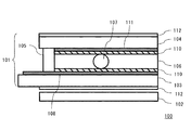
本発明の実施の形態1に係る表示装置について、図1及び図2を参照して説明する。本発明に係る表示装置は、スイッチング素子として薄膜トランジスタを有するアクティブマトリクス表示装置である。ここでは、表示装置の一例として透過型のアクティブマトリクス液晶表示装置について説明する。図1は、本実施の形態に係る液晶表示装置100の構成を示す平面図である。また、図2は本実施の形態に係る液晶表示装置100の構成を示す断面図である。なお、説明のため、図1においては対向基板等の図示を省略している。
A display device according to
図1及び図2に示すように、液晶表示装置100は、液晶表示パネル101とバックライト102とを備えている。液晶表示パネル101は、入力される表示信号に基づいて画像表示を行う。バックライト102は、液晶表示パネル101の反視認側に配置されており、液晶表示パネル101の背面側から光を照射する。液晶表示パネル101は、薄膜トランジスタアレイ基板(TFTアレイ基板)103、対向基板104、シール材105、液晶106、スペーサ107、ゲート線(走査線)108、ソース線(信号線)109、配向膜110、対向電極111、偏光板112、ゲートドライバIC113、ソースドライバIC114を備えている。本発明において注目すべき点はTFTアレイ基板103であり、後に詳述する。
As shown in FIGS. 1 and 2, the liquid
図1に示すように、本実施の形態に係る液晶表示装置100は、TFTアレイ基板103を有している。TFTアレイ基板103には、表示領域115と表示領域115を囲むように設けられた周辺領域116とが設けられている。この表示領域115には、複数のゲート線108と複数のソース線109とが形成されている。複数のゲート線108は平行に設けられている。同様に、複数のソース線109は平行に設けられている。ゲート線108と、ソース線109とは、互いに交差するように形成されている。
As shown in FIG. 1, the liquid
また、ゲート線108とソース線109の交差点付近には薄膜トランジスタ(Thin Film Transistor:TFT)118が設けられている。そして、隣接するゲート線108とソース線109とで囲まれた領域には、画素電極(不図示)が形成されている。従って、隣接するゲート線108とソース線109とで囲まれた領域が画素117となる。従って、TFTアレイ基板103上には、画素117がマトリクス状に配列される。TFT118のゲートがゲート線108に、ソースがソース線109に、ドレインが画素電極に、それぞれ接続される。画素電極は、例えば、ITO(Indium Tin Oxide)などの透明導電性薄膜から形成されている。この複数の画素117が形成されている領域が、表示領域115である。
In addition, a thin film transistor (TFT) 118 is provided in the vicinity of the intersection of the
図2に示すように、液晶表示パネル101は、TFTアレイ基板103と、TFTアレイ基板103に対向配置される対向基板104と、両基板を接着するシール材105との間の空間に液晶106を封入した構成を有している。両基板の間は、スペーサ107によって、所定の間隔となるように維持されている。TFTアレイ基板103及び対向基板104としては、例えば、光透過性のあるガラス、ポリカーボネート、アクリル樹脂などの絶縁基板が用いられる。
As shown in FIG. 2, the liquid
TFTアレイ基板103において、上述した各電極及び配線等の上には配向膜110が形成されている。一方、対向基板104のTFTアレイ基板103に対向する面には、カラーフィルタ(不図示)、BM(Black Matrix)(不図示)、対向電極111、配向膜110等が形成されている。なお、対向電極は、TFTアレイ基板103側に配置される場合もある。また、TFTアレイ基板103及び対向基板104の外側の面にはそれぞれ、偏光板112が貼着されている。
In the
さらに、図1に示すように、TFTアレイ基板103の周辺領域116には、ゲートドライバIC113及びソースドライバIC114が設けられている。ゲート線108は、表示領域115から周辺領域116まで延設されている。そして、ゲート線108は、TFTアレイ基板103の端部で、ゲートドライバIC113に接続される。ソース線109も同様に表示領域115から周辺領域116まで延設されている。そして、ソース線109は、TFTアレイ基板103の端部で、ソースドライバIC114と接続される。ゲートドライバIC113の近傍には、外部配線119が接続されている。また、ソースドライバIC114の近傍には、外部配線120が接続されている。外部配線119、119は、例えば、FPC(Flexible Printed Circuit)などの配線基板である。
Further, as shown in FIG. 1, a
外部配線119、120を介してゲートドライバIC113及びソースドライバIC114に外部から各種信号が供給される。ゲートドライバIC113は外部からの制御信号に基づいて、ゲート信号(走査信号)をゲート線108に供給する。このゲート信号によって、ゲート線108が順次選択される。ソースドライバIC114は外部からの制御信号や、表示データに基づいて表示信号をソース線109に供給する。これにより、表示データに応じた表示電圧を各画素電極に供給することができる。
Various signals are externally supplied to the
なお、ここでは、ゲートドライバIC113とソースドライバIC114は、COG(Chip On Glass)技術を用いて、TFTアレイ基板103上に直接実装したが、この構成に限られるものではない。例えば、TCP(Tape Carrier Package)によりドライバICをTFTアレイ基板103に接続してもよい。
Here, the
液晶表示パネル101の背面には、バックライト102が備えられている。バックライト102は、液晶表示パネル101の反視認側から当該液晶表示パネル101に対して光を照射する。バックライト102としては、例えば、光源、導光板、反射シート、拡散シート、プリズムシート、反射偏光シートなどを備えた一般的な構成のものを用いることができる。
A
ここで、上述の液晶表示装置100の駆動方法について説明する。各ゲート線108には、ゲートドライバIC113から走査信号が供給される。各走査信号によって、1つのゲート線108に接続されているすべてのTFT118が同時にオンとなる。そして、ソースドライバIC114から各ソース線109に表示信号が供給され、画素電極に表示信号に応じた電荷が蓄積される。表示信号が書き込まれた画素電極と対向電極111との電位差に応じて、画素電極と対向電極111間の液晶の配列が変化する。これにより、液晶表示パネル101を透過する光の透過量が変化する。画素117毎に表示電圧を変えることによって、所望の画像を表示することができる。
Here, a driving method of the liquid
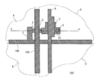
ここで、図3及び図4を参照して、本実施の形態に係る液晶表示装置100に用いられるTFTアレイ基板103について詳細に説明する。図3は、本実施の形態に係るTFTアレイ基板103上に形成されたトップゲート型のTFT118近傍の構成を示す平面図である。また、図4は、図3のa−a断面図である。本実施の形態において、TFTアレイ基板103に形成されるTFT118のチャネル活性層としては、結晶性シリコンである低温ポリシリコン(Low Temperature Poly Silicon:LTPS)を用いている。
Here, the
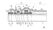
図3及び図4に示すように、TFTアレイ基板103は、絶縁基板1、ポリシリコン層2、配線層3、ゲート絶縁層4、ゲート電極5、キャパシタ電極6、層間絶縁層7、画素電極層8、コンタクトホール9、接続パッド10を有している。ここで、配線層3は、ソース線(信号線)109及び接続パッド10を含む。また、ゲート電極層11は、ゲート線(走査線)108、ゲート電極5及びキャパシタ電極6を含む。また、画素電極層8は、画素電極を含み、配線として機能する場合もある。
3 and 4, the
絶縁基板1は、ガラス基板や、導電性基板上に保護絶縁膜が形成されているものを用いることができる。絶縁基板1上には、ポリシリコン層2が形成されている。ポリシリコン層2は、ソース領域2a、チャネル領域2b、ドレイン領域2cを有する。また、絶縁基板1上において、ポリシリコン層2のソース領域2a及びドレイン領域2cの一部の上には、配線層3が形成されている。すなわち、配線層3は、ポリシリコン層2の上から絶縁基板1上にわたって形成されている。この配線層3のうち、ソース領域2aに対応した形成されているものが、ソース線109である。また、配線層3のうち、ドレイン領域2cに対応して形成されているものが、接続パッド10である。従って、配線層3は、ソース線109として機能するほか、TFT118、ストレージキャパシタ、及び画素電極層8間を所定の回路に構成する機能を有する。
As the insulating
図4に示すように、配線層3は、下敷シリコン層3a、導電層3b、界面導電層3cの3層構造となっている。配線層3のポリシリコン層2に接する界面には、下敷シリコン層3aが形成されている。下敷シリコン層3aとしては、上述したポリシリコン層2のソース領域2a、ドレイン領域2cと同一導電型の導電性不純物を含むアモルファス若しくはマイクロクリスタルシリコンを用いることができる。すなわち、配線層3は少なくとも下敷シリコン層3aとその上に形成される導電層3b及び界面導電層3cからなり、ソース領域2a及びドレイン領域2cに接する下敷シリコン層3aは、導電性不純物を含むシリコン膜である。また、下敷シリコン層3aの上に形成される導電層3b、界面導電層3cは金属膜からなる。
As shown in FIG. 4, the
導電層3bの材料としては、後の工程の熱処理に耐えるものが好ましく、高融点で導電性を有するものを用いることができる。例えば、導電層3bが、Ti、Cr、Zr、Ta、W、Mo、TiN、ZrN、TaN、WN、VNのうちの少なくとも一つを含んでいることが好ましい。なお、配線の抵抗が回路性能に大きく寄与するため、配線の低抵抗性が必要である場合には、配線層3の材料としては、Al又はCuを主成分とすることもできる。このとき、導電層3bの上に、界面導電層3cを形成する。界面導電層3cとしては、Ti、Cr、Zr、Ta、W、Mo、TiN、ZrN、TaN、WN、VNのうちの少なくとも一つを含んでいることが好ましい。すなわち、配線層3の後述する画素電極層8との界面は、高融点金属又は金属化合物である。
As a material of the
なお、本実施の形態においては、配線層3として、下敷シリコン層3a、導電層3b、界面導電層3cの3層構造としたが、これに限定されるものではない。例えば、配線層3を高融点で導電性を有する1層の導電材料で構成することも可能である。また、下敷シリコン層3aと高融点で導電性を有する材料からなる導電層3bの2層構造としてもよい。
In the present embodiment, the
また、下敷シリコン層3aを形成せず、導電層3bの材料としてCuを用いた場合、ポリシリコン層2への汚染が問題となる。この場合には、導電層3bの上側及び下側に界面導電層3cを形成することが好ましい。すなわち、導電層3bを界面導電層3cで挟み込む構造とする。すなわち、配線層3のポリシリコン層2と及び画素電極層8との界面は、それぞれTiなどの高融点金属又は金属化合物とする。
Further, when the
このように、配線層3の下側にポリシリコン層2を形成しており、配線層3のポリシリコン層2との界面は、下敷シリコン層3a又は高融点金属等である。このため、ポリシリコン層2を形成する際のレーザによる熱によって、配線層3からポリシリコン層2中に金属汚染が広がるおそれがない。従って、シリコン層に形成したTFTの接続が劣化し、リーク電流増加を抑制することができる。
Thus, the
ポリシリコン層2及び配線層3の上にはゲート絶縁層4が形成されている。ゲート絶縁層4は、ポリシリコン層2との界面で、電子や正孔のトラップ準位をつくらないことが重要である。ゲート絶縁層4としては、シリコン酸化膜などを用いることができる。また、ゲート絶縁層4上には、ポリシリコン層2のチャネル領域2bに対応して、ゲート電極5が形成されている。また、ゲート絶縁層4上には、配線層3の一部である接続パッド10に対応して、キャパシタ電極6が形成されている。ゲート電極5及びキャパシタ電極6は、同層で形成されている。図3に示すように、ゲート電極5はゲート線108としても用いられる。また、キャパシタ電極6は上述した対向電極111に共通電位を供給するための共通電位配線としても用いられる。ゲート電極5、キャパシタ電極6、ゲート線108をゲート電極層11とする。
A gate insulating layer 4 is formed on the
ゲート電極5とチャネル領域2bとを自己整合させるため、ゲート電極5を形成した後に、ゲート電極5をマスクとして、ソース領域2a及びドレイン領域2cを選択的イオン注入により形成することが好ましい。これにより、TFTの寄生容量を減らすことができる。なお、配線層3の下部のポリシリコン層2には、注入イオン量が少なくなるが、下敷シリコン層3aにより、配線層3とソース領域2a及びドレイン領域2cとの電気接続抵抗を下げることができる。さらに、下敷シリコン層3aは、ソース領域2a及びドレイン領域2cと同一導電型であるので、TFT118のオフ時のリーク電流が抑えられる。
In order to self-align the
また、キャパシタ電極6を、ゲート絶縁層4を介して配線層3の一部である接続パッド10上に形成することにより、接続パッド10をキャパシタの下部電極とすることができる。すなわち、キャパシタ電極6を上部電極とし、ゲート絶縁層4をキャパシタ絶縁膜とし、接続パッド10を下部電極とするキャパシタを形成することができる。これにより、従来のように、キャパシタの下部電極のためのドーピング工程を省略することができる。なお、キャパシタ絶縁膜として、ゲート絶縁層4以外の材料を用いたり、キャパシタ絶縁膜の膜厚を変えることによって、キャパシタ容量を変更することは可能である。
Further, by forming the
図4に示すように、ゲート電極層11上には、層間絶縁層7が形成されている。層間絶縁層7は、層間絶縁層7の下層からの水素の逸散を防止するために設けられる。層間絶縁層7の下層からの水素の逸散が生じた場合、シリコン原子のダングリングボンドが増加し、TFTの特性(閾値電圧Vth、電子移動度等)が著しく劣化してしまう。しかしながら、ゲート電極層11上に設けられた層間絶縁層7により、水素脱離によるポリシリコン層2及びポリシリコン層2とゲート絶縁層4の界面におけるシリコン原子のダングリングボンドの増加を抑えることができる。層間絶縁層7としては、少なくともシリコン窒化膜を含むことが好ましい。さらに、層間絶縁層7を形成後の熱処理により水素を拡散し、シリコン原子のダングリングボンドをさらに低減することができる。
As shown in FIG. 4, an
層間絶縁層7上には、画素電極層8が設けられている。画素電極層8は、層間絶縁層7及びゲート絶縁層4を貫くコンタクトホール9を介して、ゲート電極層11及び配線層3に電気的に接続されている。本実施の形態の場合、透過型液晶表示装置100であるため、画素電極層8としては、ITO、IZO、ITZO等の透明電極を用いる。
A
なお、ボトムエミッション型の有機EL表示装置の場合、画素電極層8としては、透過型液晶表示装置と同様に、ITO、IZO、ITZO等の透明電極を用いる。また、反射型液晶表示装置の場合には、画素電極層8としてAlや、Ag等の反射電極を用いる。また、トップエミッション型の有機EL表示装置の場合には、画素電極層8としてITO、IZO、ITZOなどの透明電極と、AlやAg等の高反射材料を積層した反射電極を用いる。
In the case of a bottom emission type organic EL display device, a transparent electrode such as ITO, IZO, ITZO or the like is used as the
画素電極層8がゲート電極層11及び配線層3と十分な電気的接続を持つために、ゲート電極層11及び配線層3上に界面導電層を形成することが好ましい。従って、本実施の形態においては、配線層3上に界面導電層3c、ゲート電極5上に界面導電層5a、キャパシタ電極6上に界面導電層6aが形成されている。この界面導電層としては、上述したように、Ti、Cr、Zr、Ta、W、Mo、TiN、ZrN、TaN、WN、VNのうちの少なくとも1つを含んでいることが好ましい。
In order for the
ここで、図5を参照して、液晶表示装置100の製造方法について説明する。図5は、本実施の形態に係る液晶表示装置100の製造方法を説明するための製造工程図である。まず、図5(a)に示すように、絶縁基板1上にポリシリコン層2を形成する。具体的には、絶縁基板1上にプラズマCVD(PECVD:Plasma Enhanced Chemical Vapor Deposition)によりアモルファスシリコン膜を形成し、XeClエキシマレーザ光(波長:308nm)若しくはYAG2ωレーザ光(波長:532nm)を照射することにより、アモルファスシリコン膜をポリシリコン膜に転換する。このポリシリコン膜を所定の形状にフォトエッチングすることにより、ポリシリコン層2を形成する。
Here, with reference to FIG. 5, the manufacturing method of the liquid
そして、図5(b)に示すように、ポリシリコン層2を形成した絶縁基板1上に配線層3を形成する。具体的には、まず、PECVDにより導電性不純物を含むアモルファスシリコン膜若しくはマイクロクリスタルシリコン膜を堆積する。下敷シリコン層3aを形成する。導電性不純物の導入は、p型不純物の場合はジボラン(B2H6)を、n型の不純物の場合はホスフィン(PH3)を、シラン(SiH4)と混合しながら、PECVD処理をすることにより行う。導電性不純物の濃度は、混合するガスの濃度で決まり、ジボラン及びホスフィンは、あらかじめ水素等で希釈して使用することが好ましい。マイクロクリスタルシリコン膜は、PECVD時の水素希釈量の最適化及び水素プラズマ処理の重畳により形成する。マイクロクリスタルシリコン膜は、ICP(Inductive Coupled Plasma)CVDにより形成することもできる。また、シランの代わりに、四フッ化珪素(SiF4)を用いてもよい。
Then, as shown in FIG. 5B, a
その後、下敷シリコン層3aの上にソース配線109を含む配線層3の材料をスパッタにより堆積させる。上述したとおり、配線層3は、後工程の熱処理に耐え、画素電極層8との電気的接合性のよい材料を用いる。あるいは、上述したとおり、配線の抵抗を低減させるため、導電層3bをAl、Cu等を用い、界面導電層3cで被覆する構成としてもよい。
Thereafter, the material of the
このように、絶縁基板1上に、下敷シリコン層3a、導電層3b、界面導電層3cからなる配線層3の材料を堆積させた後、フォトエッチングにより、所定のパターンを形成する。配線層3は、エッチングガス及び条件の異なるドライエッチングで所定のパターンを形成することができるが、配線層3のうち、導電層3b及び界面導電層3cについてはウェットエッチングで形成することも可能である。また、下敷シリコン層3aは、下層のポリシリコン層2とのエッチングレートの差を利用して選択エッチングできるように膜質の組合せを決めることが必要である。このとき、配線層3の一部は、ポリシリコン層2の一部の上に形成される。そして、配線層3は、ポリシリコン層2の上から、絶縁基板1の上まで延在して形成される。
Thus, after depositing the material of the
その後、図5(c)に示すように、ポリシリコン層2及び配線層3を覆うようにゲート絶縁層4を形成する。ゲート絶縁層4は、TEOS(Tetra Ethyl Ortho Silicate)を含むPECVDでSiO2膜を成膜することが好ましい。そして、ゲート絶縁層4の上にゲート電極5、キャパシタ電極6及びゲート配線108を含むゲート電極層11を形成する。ゲート電極層11としては、画素電極層8との電気的接合性がよいものにする必要がある。例えば、画素電極層8がITOの場合には、ITOとの電気的接合性の容易なMo合金やAl合金を選択することができる。また、ゲート電極層11の上に、ITOとの電気的接合性のよいTiNなどの界面導電層5a、6aを形成してもよい。
Thereafter, as shown in FIG. 5C, a gate insulating layer 4 is formed so as to cover the
そして、ゲート電極層11を堆積後、フォトエッチングにより、ゲート電極5及びキャパシタ電極6などを所定の形状にパターニングする。エッチングは、ウェットエッチングあるいはドライエッチングで行うことができる。これにより、ゲート絶縁層4を介して、ゲート電極5とポリシリコン層2とが対向するように形成される。また、ゲート絶縁層4を介して、キャパシタ電極6と配線層3の一部である接続パッド10とが対向するように形成される。すなわち、キャパシタ電極6は、接続パッド10の一部と重畳する。
Then, after depositing the
ゲート電極5を形成した後、ゲート電極5とポリシリコン層2のチャネル領域2bを自己整合させるために、ゲート電極5をマスクとして、ソース領域2a及びドレイン領域2cを選択的にイオン注入する。これにより、ポリシリコン層2にソース領域2a及びドレイン領域2cを形成する。なお、配線層3の下部のポリシリコン層2では、注入イオン量が少なくなるが、下敷シリコン層3aにより配線層3とソース領域2a及びドレイン領域2cとの電気接続抵抗を下げることができる。
After the
また、ゲート絶縁層4上に、キャパシタ電極6を配線層3の一部である接続パッド10に対応して形成することにより、キャパシタ電極6を上部電極、接続パッド10を下部電極としたキャパシタを形成することができる。このとき、キャパシタ電極6を接続パッド10との間に形成されるゲート絶縁層4がキャパシタ絶縁層となる。なお、キャパシタ絶縁層として、ゲート絶縁層4以外の材料を用いてもよく、キャパシタ絶縁膜の膜厚をゲート絶縁層4の膜厚と異なるようにして、キャパシタ容量を変更することも可能である。
Further, the
次いで、図5(d)に示すように、ゲート絶縁層4、ゲート電極層11を覆うように層間絶縁層7を形成する。層間絶縁層7としては、上述したように、水素の逸散を防止する膜、つまりPECVDにより形成したシリコン窒化膜を含む膜を用いることができる。また、層間絶縁層7として、TEOSを含むPECVDで形成したシリコン酸化膜を下層とし、PECVDで形成したシリコン窒化膜を上層にした二層構造とすることが更に好ましい。
Next, as illustrated in FIG. 5D, an
そして、層間絶縁層7及びゲート絶縁層4の所定の位置にコンタクトホール9を形成する。これにより、接続パッド10の一部を露出させる。コンタクトホール9の形成は、ドライエッチングを用いることができる。一般に、シリコン酸化膜及びシリコン窒化膜からなる層間絶縁層7と、ポリシリコン層2のドライエッチングにおける選択性は低い。このため、従来のように、直接ポリシリコン層2上にコンタクトホールを形成した場合、ポリシリコン層2までもエッチングされてしまうこととなるエッチングの突き抜けが発生する。しかしながら、本実施の形態によれば、コンタクトホール9は、ポリシリコン層2上に直接形成されず、ポリシリコン層2に接続する配線層3上に形成される。このため、安定した形状のコンタクトホール9を得ることができる。
Then, contact holes 9 are formed at predetermined positions of the interlayer insulating
その後、図5(e)に示すように、層間絶縁層7上に画素電極を含む画素電極層8を形成する。これにより、画素電極層8の画素電極は、層間絶縁層7及びゲート絶縁層4を貫くコンタクトホール9を介して、配線層3の一部である接続パッド10に電気的に接続される。また、ここでは図示していないが、画素電極層8の一部は、ゲート電極層11で絶縁基板1の端部に形成される端子等にも電気的に接続される。画素電極層8としては、上述のとおり、ITO等の透明電極を用いることができる。そして、層間絶縁層7上に堆積された画素電極材料を所定の形状にフォトエッチングして、画素電極等を形成する。
Thereafter, as shown in FIG. 5E, a
このようにして、TFTアレイ基板103が形成される。その後、このようにして形成されたTFTアレイ基板を用いて液晶パネル101を形成し、バックライト102、ゲートドライバIC113、ソースドライバIC114等を実装して、本実施の形態に係る液晶表示装置100を得ることができる。
In this way, the
このように、本発明に係る液晶表示装置の製造方法においては、ストレージキャパシタの下部電極として、配線層3の一部を用いることができる。このため、従来のように、ストレージキャパシタの下部電極用のポリシリコン層の低抵抗化のためのドーピング工程が必要ない。また、配線層3が直接ポリシリコン層2のソース領域2a及び、ドレイン領域2c上に設けられているため、ソース・ドレイン配線用のコンタクトホール形成工程が必要なくなる。このように、製造工程を省略することができ、生産性を向上させることができる。
Thus, in the method for manufacturing the liquid crystal display device according to the present invention, a part of the
実施の形態2.
本発明の実施の形態2に係る表示装置について、図6を参照して説明する。図6は、本実施の形態に係る液晶表示装置100に用いられるTFTアレイ基板103の構成を示す断面図である。本実施の形態において、実施の形態1と異なる点は、画素電極層8の一部が絶縁基板1に接しており、画素電極層8が絶縁基板1に接する領域の近傍で、画素電極層8と配線層3とが接続されている点である。また、本実施の形態に係る液晶表示装置100は、配線層3を反射電極とし、画素電極層8を透明電極とする半透過型液晶表示装置に適している。このため、本実施の形態においては、半透過型の液晶表示装置100について説明する。図6において図4と同一の構成要素には同一の符号を付し、説明を省略する。また、本実施の形態においてTFTアレイ基板103以外の他の構成要素については、図1及び図2に示すものと同一の物を用いることができる。従って、ここでは、図6に示すTFTアレイ基板103の構成について説明する。
A display device according to
図6に示すように、本実施の形態に用いられるTFTアレイ基板103は、絶縁基板1、ポリシリコン層2、配線層3、ゲート絶縁層4、ゲート電極5、キャパシタ電極6、層間絶縁層7、画素電極層8、接続パッド10、ゲート電極層11などを有している。絶縁基板1上には、ソース領域2a、チャネル領域2b、ドレイン領域2cを有するポリシリコン層2が形成されている。ポリシリコン層2の一部の上には、配線層3が形成されている。配線層3の一部であるソース線109は、ポリシリコン層2のソース領域2aの上から絶縁基板1にわたって形成されている。また、配線層3の一部である接続パッド10は、ポリシリコン層2のドレイン領域2cの上から絶縁基板1に延在して形成されている。なお、絶縁基板1上には、後述する画素電極層8が形成されている。また、画素電極層8は、層間絶縁層7の上及び配線層3の上にも形成される。すなわち、画素電極層8は、層間絶縁層7上から、配線層3及び絶縁基板1上にわたって形成されている。
As shown in FIG. 6, the
本実施の形態においては、配線層3は、反射特性を有する材料からなる。例えば、配線層3を構成する導電層3bをAl、Agなどとすることができる。そして、配線層3は、実施の形態1において説明したように、下敷シリコン層3a、導電層3b、界面導電層3cの3層構造とする。これにより、配線層3のうち接続パッド10の一部を反射電極として利用することができる。
In the present embodiment, the
ポリシリコン層2及び配線層3の上には、ゲート絶縁層4が形成されている。また、ゲート絶縁層4は、接続パッド10の一部の上に形成される。接続パッド10上において、ゲート絶縁層4が形成されていない領域には、画素電極層8が直接形成されている。すなわち、接続パッド10と画素電極層8とは、直接接続される。このように、本実施の形態においては、画素電極層8に画像信号を伝送するための配線層3と、画素電極層8との接続面積を比較的広くすることができる。また、画素電極層8と接続パッド10とを接続するためのコンタクトホールを形成する必要がない。しかしながら、配線層3と画素電極層8との接続のためのコンタクトホールの代わりに、図6においては図示していないが、配線層3とゲート電極5との接続のために後述する層間絶縁層7にコンタクトホールを形成する必要がある。このため、図4に示す実施の形態1と同じ製造工程数で形成することができる。
A gate insulating layer 4 is formed on the
ゲート絶縁層4上には、ゲート電極5及びキャパシタ電極6を含む、ゲート電極層11が形成されている。ゲート絶縁層4上において、ゲート電極5はポリシリコン層2のチャネル領域2bに対応して形成されており、キャパシタ電極6は、配線層3の接続パッド10に対応して形成されている。従って、本実施の形態においては、配線層の一部である接続パッド10が、キャパシタの下部電極として利用することできる。このため、ストレージキャパシタの下部電極用のポリシリコン層の低抵抗化のためのドーピング工程、及び、ソース・ドレイン配線用のコンタクトホール形成工程の2つの工程を省略することができる。
A
ゲート電極層11の上には、層間絶縁層7が形成されている。そして、層間絶縁層7上には、画素電極層8が形成されている。このため、上述したように、画素電極層8は、層間絶縁層7の上から接続パッド10上及び絶縁基板1上にわたって形成されている。画素電極層8としては、ITO等からなる透明導電材料を用いる。ゲート線108及びソース線109で囲まれた画素117のうち、反射電極である接続パッド10及び画素電極8aが形成された領域が反射領域117aである。また、画素117のうち、透明電極である画素電極8aが配置された領域のうち、接続パッド10が形成されている領域が透過領域117bである。
On the
このとき、反射電極として機能する接続パッド10上の画素電極層8をできるだけ除去することが好ましい。これにより、反射電極である接続パッド10の反射率を増大させることができ、反射モードにおける輝度を向上させることが可能となる。また、反射電極である接続パッド10上の界面導電層3cを除去することにより、反射率をさらに増大させることができる。
At this time, it is preferable to remove as much as possible the
実施の形態3.
本発明の実施の形態3に係る表示装置について、図7を参照して説明する。図7は、本実施の形態に係る液晶表示装置100に用いられるTFTアレイ基板103の構成を示す断面図である。本実施の形態において、実施の形態1と異なる点は、配線層3のポリシリコン層2との界面に形成される下敷シリコン層3aの代わりに界面導電層3cが設けられている点である。図7において、図4と同一の構成要素には、同一の符号を付し、説明を省略する。また、本実施の形態においてTFTアレイ基板103以外の他の構成要素については、図1及び図2に示すものと同一の物を用いることができる。従って、ここでは、図7に示すTFTアレイ基板103の構成について説明する。
A display device according to
図7に示すように、本実施の形態に用いられるTFTアレイ基板103は、絶縁基板1、ポリシリコン層2、配線層3、ゲート絶縁層4、ゲート電極5、キャパシタ電極6、層間絶縁層7、画素電極層8、接続パッド10、ゲート電極層11などを有している。絶縁基板1上には、ソース領域2a、チャネル領域2b、ドレイン領域2cを有するポリシリコン層2が形成されている。ポリシリコン層2の一部の上には、配線層3が形成されている。配線層3の一部であるソース線109は、ポリシリコン層2のソース領域2aの上から絶縁基板1にわたって形成されている。また、配線層3の一部である接続パッド10は、ポリシリコン層2のドレイン領域2cの上から絶縁基板1に延在して形成されている。本実施の形態においては、配線層3のポリシリコン層2との界面には、下敷シリコン層3aを形成しない構成とする。すなわち、配線層3は、図7に示すように、導電層3bを界面導電層3cにより挟み込んだ3層構造とすることができる。
As shown in FIG. 7, the
また、ポリシリコン層2及び配線層3の上には、ゲート絶縁層4が形成されている。そして、ゲート絶縁層4上には、ゲート電極5及びキャパシタ電極6を含む、ゲート電極層11が形成されている。ゲート絶縁層4上において、ゲート電極5はポリシリコン層2のチャネル領域2bに対応して形成されており、キャパシタ電極6は、配線層3の接続パッド10に対応して形成されている。従って、本実施の形態においては、配線層の一部である接続パッド10が、キャパシタの下部電極として利用することできる。このため、ストレージキャパシタの下部電極用のポリシリコン層の低抵抗化のためのドーピング工程、及び、ソース・ドレイン配線用のコンタクトホール形成工程の2つの工程を省略することができる。なお、また、キャパシタ絶縁膜としてゲート絶縁層4以外の材料等を用いることにより、キャパシタ容量を変更することが可能である。
A gate insulating layer 4 is formed on the
実施の形態1において説明したように、ゲート電極5とチャネル領域2bとを自己整合させるために、ゲート電極5を形成した後に、ゲート電極5をマスクとして、ソース領域2a、ドレイン領域2cを選択的にイオン注入することによって形成する。このとき、ポリシリコン層2のソース領域2a、ドレイン領域2c上に形成された配線層3は、イオン注入の際の障害となる。このため、イオン注入時には、イオン注入部のゲート絶縁層4の膜厚を削減したり、配線層3の膜厚を削減する等の工夫が必要である。
As described in the first embodiment, in order to self-align the
また、配線層3の導電層3b及び界面導電層3cとしては、比較的イオンストッピングパワーが低い材料を用いることが好ましい。SRIM(the Stopping and Range of Ions in Matter; James F. Ziegler)によれば、イオンエネルギー100〜200KeVにおけるイオンストッピングパワーの順位は、次のようになる。
リンイオンのイオンストッピングパワー順位;Si<Al<Ti<Zr≦Sn<Cu
ボロンイオンのストッピングパワー順位;Si<Al<Ti≦Zr<Sn<Cu
In addition, as the
Phosphorus ion stopping power ranking; Si <Al <Ti <Zr ≦ Sn <Cu
Boron ion stopping power ranking; Si <Al <Ti ≦ Zr <Sn <Cu
上記のイオンストッピングパワー順位から、配線層3の導電層3bとしては、Al、界面導電層3cとしては、Ti、Zr及び導電性のTi、Zr化合物を用いることができる。あるいは、配線層3をTi、Zr及び導電性のTi、Zr化合物の単層としてもよい。ただし、配線抵抗の観点から、Alからなる導電層3bと、界面導電層3cの組合せを用いることが好ましい。
From the above ion stopping power ranking, Al can be used as the
また、n型領域形成のためのリンイオンの注入深さは、同じ注入エネルギーで比較すると、p型領域形成のボロンイオンの注入深さの約1/3である。このため、n型領域形成のためのイオン注入が難しい。このため、リンイオンを注入する場合、上述したSRIMによれは、対象領域のゲート絶縁層4の膜厚を30nm、配線層3の導電層3bのAlの膜厚を65nm、界面導電層3cのTiの膜厚を20nmとして、リンイオンをポリシリコン層2へ注入するための注入エネルギーは、100KeV以上であることが必要である。配線層3の導電層3bのAlの膜厚を160nm、界面導電層3cのTiの膜厚を200nmとした場合は、リンイオンをポリシリコン層2へ注入するための注入エネルギーは、200KeVが必要である。
Further, the phosphorus ion implantation depth for forming the n-type region is about 1/3 of the boron ion implantation depth for forming the p-type region when compared with the same implantation energy. For this reason, ion implantation for forming the n-type region is difficult. Therefore, when phosphorus ions are implanted, according to the SRIM described above, the thickness of the gate insulating layer 4 in the target region is 30 nm, the thickness of the Al of the
一方、ボロンイオンを注入する場合、上述したSRIMによれば、ゲート絶縁層4を30nm、配線層3の導電層3bのAl膜厚を210nm、及び、界面導電層3cのTi膜厚を20nmとして、ポリシリコン層2へのボロンイオンを注入するための注入エネルギーは、100KeV以上となり、p型領域の形成のほうがn型領域の形成と比較するとはるかに容易である。
On the other hand, when boron ions are implanted, according to the SRIM described above, the gate insulating layer 4 is 30 nm, the Al film thickness of the
そして、図7に示すように、ゲート電極層11の上には、層間絶縁層7が形成されている。また、層間絶縁層7及びゲート絶縁層4の所定の位置には、コンタクトホール9が形成されている。層間絶縁層7上には、画素電極層8が設けられている。画素電極層8は、層間絶縁層7及びゲート絶縁層4を貫くコンタクトホール9を介して、ゲート電極層11及び配線層3に電気的に接続されている。また、画素電極層8は、層間絶縁層7の上から接続パッド10上及び絶縁基板1上にわたって形成されている。
Then, as shown in FIG. 7, an
このように、配線層3のポリシリコン層2との界面に、下敷シリコン層3aを形成しなくても、配線層3、ゲート絶縁層4等の膜厚を調整することによって、適切にポリシリコン層にイオンをドープすることができる。
Thus, even if the
実施の形態4.
本発明の実施の形態4に係る表示装置について、図8を参照して説明する。図8は、本実施の形態に係る液晶表示装置100に用いられるTFTアレイ基板103の構成を示す断面図である。本実施の形態において、実施の形態1と異なる点は、ソース領域2a上の配線層3が、チャネル領域2bに接している点である。すなわち、配線層3はチャネル領域2bの上まで設けられている。図8において、図4と同一の構成要素には、同一の符号を付し説明を省略する。また、本実施の形態においてTFTアレイ基板103以外の他の構成要素については、図1及び図2に示すものと同一の物を用いることができる。従って、ここでは、図8に示すTFTアレイ基板103の構成について説明する。
Embodiment 4 FIG.
A display device according to Embodiment 4 of the present invention will be described with reference to FIG. FIG. 8 is a cross-sectional view showing the configuration of the
図8に示すように、本実施の形態に用いられるTFTアレイ基板103は、絶縁基板1、ポリシリコン層2、配線層3、ゲート絶縁層4、ゲート電極5、キャパシタ電極6、層間絶縁層7、画素電極層8、接続パッド10、ゲート電極層11などを有している。絶縁基板1上には、ソース領域2a、チャネル領域2b、ドレイン領域2cを有するポリシリコン層2が形成されている。
As shown in FIG. 8, the
ポリシリコン層2の一部の上には、配線層3が形成されている。配線層3の一部であるソース線109は、ポリシリコン層2のソース領域2aの上から絶縁基板1にわたって形成されている。本実施の形態においては、ソース線109は、チャネル領域2bに接している。すなわち、ソース線109は、後述するゲート電極5の下側まで延設されている。つまり、ソース線109チャネル領域2bの上まで設けられている。なお、配線層3のポリシリコン層2との界面には、下敷シリコン層3aが形成されている。このため、配線層3の導電層3bと、チャネル領域2bとがショートすることはない。また、配線層3の一部である接続パッド10は、ポリシリコン層2のドレイン領域2cの上から絶縁基板1に延在して形成されている。
A
また、ポリシリコン層2及び配線層3の上には、ゲート絶縁層4が形成されている。そして、ゲート絶縁層4上には、ゲート電極5及びキャパシタ電極6を含む、ゲート電極層11が形成されている。ゲート絶縁層4上において、ゲート電極5はポリシリコン層2のチャネル領域2bに対応して形成されており、キャパシタ電極6は、配線層3の接続パッド10に対応して形成されている。従って、本実施の形態においては、配線層の一部である接続パッド10が、キャパシタの下部電極として利用することできる。このため、ストレージキャパシタの下部電極用のポリシリコン層の低抵抗化のためのドーピング工程、及び、ソース・ドレイン配線用のコンタクトホール形成工程の2つの工程を省略することができる。なお、また、キャパシタ絶縁膜としてゲート絶縁層4以外の材料等を用いることにより、キャパシタ容量を変更することが可能である。また、本実施の形態においては、ゲート電極5は、ソース線109の上に対応する位置にも形成されている。
A gate insulating layer 4 is formed on the
このような構成とすることによって、TFT118の寄生抵抗で影響が大きいソース抵抗を低減させることができる。特に、ソース領域2a及びドレイン領域2cがチャネル領域に接する部分の導電性不純物濃度を低減するLDD(Lightly Doped Drain)構造や、GOLD(Gate Overlapped LDD)構造で、プロセス上ソース領域も同じ構造とする場合には、ソース側の抵抗増大を解消することができ、TFTの寄生抵抗を低減させることができる。
By adopting such a configuration, it is possible to reduce the source resistance that is greatly affected by the parasitic resistance of the
実施の形態5.
本発明の実施の形態5に係る表示装置について、図9を参照して説明する。図9は本実施の形態に係る液晶表示装100に用いられるTFTアレイ基板103の構成を示す断面図である。本実施の形態において、実施の形態1と異なる点は、ソース領域2a上の配線層3及びドレイン領域2c上の配線層3が、チャネル領域2bに接している点である。すなわち、配線層3はチャネル領域2bの上まで設けられている。図9において、図4と同一の構成要素には、同一の符号を付し説明を省略する。また、本実施の形態においてTFTアレイ基板103以外の他の構成要素については、図1及び図2に示すものと同一の物を用いることができる。従って、ここでは、図9に示すTFTアレイ基板103の構成について説明する。
A display device according to
図9に示すように、本実施の形態に用いられるTFTアレイ基板103は、絶縁基板1、ポリシリコン層2、配線層3、ゲート絶縁層4、ゲート電極5、キャパシタ電極6、層間絶縁層7、画素電極層8、接続パッド10、ゲート電極層11などを有している。絶縁基板1上には、ソース領域2a、チャネル領域2b、ドレイン領域2cを有するポリシリコン層2が形成されている。
As shown in FIG. 9, the
ポリシリコン層2の一部の上には、配線層3が形成されている。配線層3の一部であるソース線109は、ポリシリコン層2のソース領域2aの上から絶縁基板1にわたって形成されている。本実施の形態においては、ソース線109は、チャネル領域2bに接している。すなわち、ソース線109は、後述するゲート電極5の下側まで延設されている。つまり、ソース線109はチャネル領域2bの上まで設けられている。また、配線層3の一部である接続パッド10は、ポリシリコン層2のドレイン領域2cの上から絶縁基板1に延在して形成されている。接続パッド10は、チャネル領域2bに接している。すなわち、接続パッド10は、後述するゲート電極5の下側まで延設されている。つまり、接続パッド10はチャネル領域2bの上まで設けられている。なお、配線層3のポリシリコン層2との界面には、下敷シリコン層3aが形成されている。このため、配線層3の導電層3bと、チャネル領域2bとがショートすることはない。
A
また、ポリシリコン層2及び配線層3の上には、ゲート絶縁層4が形成されている。そして、ゲート絶縁層4上には、ゲート電極5及びキャパシタ電極6を含む、ゲート電極層11が形成されている。ゲート絶縁層4上において、ゲート電極5はポリシリコン層2のチャネル領域2bに対応して形成されており、キャパシタ電極6は、配線層3の接続パッド10に対応して形成されている。従って、本実施の形態においては、配線層の一部である接続パッド10が、キャパシタの下部電極として利用することできる。このため、ストレージキャパシタの下部電極用のポリシリコン層の低抵抗化のためのドーピング工程、及び、ソース・ドレイン配線用のコンタクトホール形成工程の2つの工程を省略することができる。なお、また、キャパシタ絶縁膜としてゲート絶縁層4以外の材料等を用いることにより、キャパシタ容量を変更することが可能である。また、本実施の形態においては、ゲート電極5は、ソース線109の上に対応する位置にも形成されている。
A gate insulating layer 4 is formed on the
このような構成とすることによって、TFT118の寄生抵抗で影響が大きいソース・ドレイン抵抗を低減させることができる。さらに、ソース領域2a及びドレイン領域2cが配線層3で覆われているため、ソース領域2a及びドレイン領域2cの形成に必要な導電性不純物のイオン注入工程を省略することができる。また、下敷シリコン層3aの不純物濃度を制御することにより、ドレイン領域2cとチャネル領域2bとの界面の電界強度を押さえて、LDDと同様な効果を得ることができる。
By adopting such a configuration, it is possible to reduce the source / drain resistance that is greatly affected by the parasitic resistance of the
実施の形態6.
本発明の実施の形態6に係る表示装置について、図10及び図11を参照して説明する。図10は、本実施の形態に係る液晶表示装置100の構成を示す平面図である。また、図11は、図10のb−b断面図である。本実施の形態においては、実施の形態1〜5と異なり、ポリシリコン層2上に直接配線層3が接続されていない。なお、図10及び図11において、図3及び図4と同一の構成要素には、同一の符号を付し説明を省略する。また、本実施の形態においてTFTアレイ基板103以外の他の構成要素については、図1及び図2に示すものと同一の物を用いることができる。従って、ここでは、図10及び図11に示すTFTアレイ基板103の構成について説明する。
A display device according to
図10及び図11に示すように、TFTアレイ基板103は、絶縁基板1、ポリシリコン層2、配線層3、ゲート絶縁層4、ゲート電極5、キャパシタ電極6、層間絶縁層7、画素電極層8、コンタクトホール9、接続パッド10を有している。ここで、配線層3は、ソース線(信号線)109及び接続パッド10を含む。また、ゲート電極層11は、ゲート線(走査線)108、ゲート電極5及びキャパシタ電極6を含む。また、画素電極層8は、画素電極を含み、配線として機能する場合もある。
As shown in FIGS. 10 and 11, the
絶縁基板1上には、ポリシリコン層2が形成されている。ポリシリコン層2は、ソース領域2a、チャネル領域2b、ドレイン領域2cを有する。また、絶縁基板1上には、ポリシリコン層2と独立して形成された配線層3が形成されている。すなわち、配線層3は、ポリシリコン層2と相互接触しないように形成されている。つまり、配線層3は、ポリシリコン層2から離間して形成されている。配線層3は、ソース線109として機能するほか、TFT118、ストレージキャパシタ、及び画素電極層8間を所定の回路に構成する機能を有する。図11に示すように、本実施の形態においては、導電層3b、界面導電層3cの2層構造としている。絶縁基板1上には、導電層3bが形成されている。そして、導電層3b上には、画素電極層8と接する界面導電層3cが形成されている。すなわち、配線層3は、導電層3bと界面導電層3cをこの順に絶縁基板1上に形成した構成を有している。なお、上述したように、配線層3は、Ti等の高融点導電材料からなる単層であってもよく、Alなどの導電層3bを高融点導電材料の界面導電層3cにより被覆したものを用いてもよい。従って、配線層3の画素電極層8との界面は、高融点金属又は金属化合物である。
A
ポリシリコン層2及び配線層3上には、ゲート絶縁層4が形成されている。また、ゲート絶縁層4上には、ポリシリコン層2のチャネル領域2bに対応して、ゲート電極5が形成されている。さらに、ゲート絶縁層4上には、配線層3の一部である接続パッド10に対応して、キャパシタ電極6が形成されている。ゲート電極5及びキャパシタ電極6は、同層で形成されている。図10に示すように、ゲート電極5はゲート線108としても用いられる。また、キャパシタ電極6は上述した対向電極111に共通電位を供給するための共通電位配線としても用いられる。ゲート電極5、キャパシタ電極6、ゲート線108をゲート電極層11とする。
A gate insulating layer 4 is formed on the
また、画素電極層8がゲート電極層11及び配線層3と十分な電気的接続を持つために、ゲート電極層11及び配線層3上に界面導電層を形成することが好ましい。従って、本実施の形態においては、配線層3上に界面導電層3c、ゲート電極5上に界面導電層5a、キャパシタ電極6上に界面導電層6aが形成されている。この界面導電層としては、上述したように、Ti、Cr、Zr、Ta、W、Mo、TiN、ZrN、TaN、WN、VNのうちの少なくとも1つを含んでいることが好ましい。
Further, in order for the
また、キャパシタ電極6をゲート絶縁層4を介して配線層3の一部である接続パッド10の上に形成することにより、この一部の接続パッド10をキャパシタの下部電極とすることができる。すなわち、キャパシタ電極6を上部電極とし、ゲート絶縁層4をキャパシタ絶縁膜とし、接続パッド10を下部電極とするキャパシタを形成することができる。これにより、キャパシタの下部電極のためのドーピング工程を省略することができる。なお、キャパシタ絶縁膜として、ゲート絶縁層4以外の材料を用いたり、キャパシタ絶縁膜の膜厚を変えることによって、キャパシタ容量を変更することは可能である。
Further, by forming the
図11に示すように、ゲート電極層11上には、層間絶縁層7が形成されている。層間絶縁層7は、層間絶縁層7の下層からの水素の逸散を防止するために設けられる。上述のとおり、層間絶縁層7としては、少なくともシリコン窒化膜を含む膜を用いることによって、水素脱離によるポリシリコン層2及びポリシリコン層2とゲート絶縁層4の界面におけるシリコン原子のダングリングボンドの増加を抑えることができる。また、層間絶縁層7を形成後の熱処理により水素を拡散し、シリコン原子のダングリングボンドをさらに低減することができる。層間絶縁層7の所定の位置には、コンタクトホール9が設けられている。ここで、コンタクトホール9aは画素電極層8からなる画素電極8aと接続パッド10とを接続するために設けられており、コンタクトホール9bは画素電極8aとポリシリコン層2のドレイン領域2cとを接続するために設けられている。また、コンタクトホール9cは画素電極層8からなる接続電極8bとポリシリコン層2のソース領域2aとを接続するために設けられており、コンタクトホール9dは接続電極8bと配線層3の一部であるソース配線109とを接続するために設けられている。
As shown in FIG. 11, an
層間絶縁層7上には、画素電極層8が設けられている。画素電極層8は、画素電極8aと接続電極8bとからなる。画素電極8aは、層間絶縁層7及びゲート絶縁層4を貫くコンタクトホール9a、9bを介して、接続パッド10、ドレイン領域2cにそれぞれ接続されている。また、接続電極8bは、層間絶縁層7及びゲート絶縁層4を貫くコンタクトホール9c、9dを介して、ソース領域2a、ソース配線109にそれぞれ接続されている。本実施の形態の場合、透過型液晶表示装置100であるため、画素電極層8としては、ITO、IZO、ITZO等の透明電極を用いる。なお、上述のとおり、反射型液晶表示装置、ボトムエミッション型の有機EL表示装置、トップエミッション型の有機EL表示装置の場合には、それぞれ適した画素電極層8の材料を用いる。
A
画素電極層8がITO、IZO、ITZO等の金属酸化膜の場合、ポリシリコン層2のソース領域2a及びドレイン領域2cとの接続は、ポリシリコン層2の界面にシリコン酸化膜が成長し、電気的接続が難しい。従って、本実施の形態においては、画素電極層8を形成する前に、ポリシリコン層2と画素電極層8との接続部にシリサイド層2dを形成している。すなわち、ポリシリコン層2は、画素電極層8との界面にシリサイド層2dを有する。これにより、ポリシリコン層2と画素電極層8との電気的接続性を改善することができる。
When the
シリサイド層2dの形成のためには、比較的低温でポリシリコンとシリサイド化する金属で、かつ金属酸化膜が導電性を有することが必要である。この点を考慮し、シリサイド化させる金属としては、Co、Ni、Mo、W、Crを使用することが好ましい。特に、Coは、400℃程度の熱処理でポリシリコン層2と簡単にシリサイドを形成するため好ましい。600℃以上の高温処理が必要な場合には、ランプアニーリングRTA(Rapid Thermal Annealing)処理により、絶縁基板1の熱歪を抑えてシリサイド化することが好ましい。シリサイド化量は、電気的接続抵抗の必要に応じて調整することが可能である。
In order to form the
ここで、図12を参照して、本実施の形態に係る液晶表示装置100の製造方法について説明する。図12は、本実施の形態に係る液晶表示装置100の製造工程を説明するための製造工程図である。なお、本実施の形態において、実施の形態1の製造方法における工程と同一の工程の説明については、適宜省略する。
Here, with reference to FIG. 12, a method of manufacturing liquid
まず、図12(a)に示すように、絶縁基板1上に、ポリシリコン層2を形成する。上述したように、a−Si膜を形成した後、レーザアニーリングすることによって、ポリシリコン層2を形成することができる。そして、図12(b)に示すように、ポリシリコン層2を形成した絶縁基板1上に、ポリシリコン層2と相互接触しないように、配線層3を形成する。具体的には、絶縁基板1上に導電層3b及び界面導電層3cの材料をスパッタにより堆積させた後、フォトエッチングにより、所定のパターンを形成する。これにより、絶縁基板1上に配線層3がポリシリコン層2から離間して形成される。
First, as shown in FIG. 12A, a
その後、図12(c)に示すように、ポリシリコン層2及び配線層3を覆うように、ゲート絶縁層4を形成する。ゲート絶縁層4は、上述のとおり、TEOS(Tetra Ethyl Ortho Silicate)を含むPECVDでSiO2膜を成膜することが好ましい。そして、ゲート絶縁層4の上にゲート電極5、キャパシタ電極6及びゲート配線108を含むゲート電極層11を形成する。また、ゲート電極層11の上に、ITOとの電気的接合性のよいTiNなどの界面導電層5a、6aを形成する。そして、ゲート電極層11を堆積後、フォトエッチングにより、ゲート電極5及びキャパシタ電極6などを所定の形状にパターニングする。これにより、ゲート絶縁層4を介して、ゲート電極5とポリシリコン層2とが対向するように形成される。また、ゲート絶縁層を介して、キャパシタ電極6と配線層3の一部である接続パッド10とが対向するように形成される。
Thereafter, as shown in FIG. 12C, a gate insulating layer 4 is formed so as to cover the
ゲート電極5を形成した後、ゲート電極5とポリシリコン層2のチャネル領域2bを自己整合させるために、ゲート電極5をマスクとして、ソース領域2a及びドレイン領域2cを選択的にイオン注入する。これにより、ポリシリコン層2にソース領域2a及びドレイン領域2cを形成する。
After the
また、ゲート絶縁層4上に、キャパシタ電極6を配線層3の一部である接続パッド10に対応して形成することにより、キャパシタ電極6を上部電極、接続パッド10を下部電極としたキャパシタを形成することができる。このとき、キャパシタ電極6を接続パッド10との間に形成されるゲート絶縁層4がキャパシタ絶縁層となる。なお、キャパシタ絶縁層として、ゲート絶縁層4以外の材料を用いてもよく、キャパシタ絶縁膜の膜厚をゲート絶縁層4の膜厚と異なるようにして、キャパシタ容量を変更することも可能である。
Further, the
次いで、図12(d)に示すように、ゲート絶縁層4、ゲート電極層11を覆うように層間絶縁層7を形成する。層間絶縁層7としては、上述したように、水素の逸散を防止する膜、つまりPECVDにより形成したシリコン窒化膜を含むものを用いることができる。また、層間絶縁層7として、TEOSを含むPECVDで形成したシリコン酸化膜を下層とし、PECVDで形成したシリコン窒化膜を上層にした二層構造とすることが更に好ましい。
Next, as illustrated in FIG. 12D, the
そして、層間絶縁層7及びゲート絶縁層4の所定の位置にコンタクトホール9を形成する。これにより、配線層3の接続パッド10及びソース配線109の一部、ポリシリコン層2のソース領域2a及びドレイン領域2cの一部を露出させる。コンタクトホール9の形成は、ドライエッチングを用いることができる。
Then, contact holes 9 are formed at predetermined positions of the interlayer insulating
その後、コンタクトホール9b及び9cの底部に、シリサイド層2dを形成する。具体的には、層間絶縁層7上及びコンタクトホール9内面にシリサイド層2dを形成するための金属膜をスパッタにより堆積させる。すなわち、コンタクトホール9b及びコンタクトホール9cの底部のポリシリコン層2上に、シリサイド層2d形成用の金属膜が形成される。そして、ポリシリコン層2と金属膜の積層膜を、高温でアニールすることによりシリサイド層2dを形成することができる。例えば、Coをスパッタにより堆積させ、400℃の熱処理を行うことにより、Coとポリシリコン層2とのシリサイドを形成することができる。これにより、画素電極層8とポリシリコン層2との電気的接続性を改善することができる。なお、600℃以上の高温が必要な場合はランプアニーリング等のRTA(Rapid Thermal Annealing)処理により、ガラス基板の熱歪を抑えてシリサイド化することが好ましい。そして、熱処理を行い、ポリシリコン層2の表面にシリサイド層2dを形成した後、不要なシリサイド層形成用の金属膜をウェットエッチングで除去する。これにより、図12(e)に示すように、ポリシリコン層2のソース領域2a上に設けられたコンタクトホール9cの底部及びドレイン領域2c上に設けられたコンタクトホール9bの底部にシリサイド層2dを形成することができる。なお、層間絶縁層7上の残渣は、表面を軽くエッチオフすることが好ましい。このシリサイド化により、画素電極層8からのポリシリコン層2への汚染が防止できる。
Thereafter, a
その後、図12(f)に示すように、層間絶縁層7上に画素電極8a及び接続電極8bを含む画素電極層8を形成する。これにより、画素電極8aは、層間絶縁層7及びゲート絶縁層4を貫くコンタクトホール9aを介して、配線層3の一部である接続パッド10に電気的に接続される。また、画素電極8aは、層間絶縁層7及びゲート絶縁層4を貫くコンタクトホール9bを介して、ポリシリコン層2のドレイン領域2cに電気的に接続される。一方、接続電極8bは、層間絶縁層7及びゲート絶縁層4を貫くコンタクトホール9cを介して、ポリシリコン層2のソース領域2aに電気的に接続される。また、接続電極8bは、層間絶縁層7及びゲート絶縁層4を貫くコンタクトホール9dを介して、配線層3の一部であるソース線109に電気的に接続される。なお、ここでは図示していないが、画素電極層8の一部は、ゲート電極層11で絶縁基板1の端部に形成される端子等にも電気的に接続される。画素電極層8としては、上述のとおり、ITO等の透明電極を用いることができる。そして、層間絶縁層7上に堆積された画素電極材料を所定の形状にフォトエッチングして、画素電極等を形成する。
Thereafter, as shown in FIG. 12 (f), the
このようにして、TFTアレイ基板103が形成される。その後、このようにして形成されたTFTアレイ基板を用いて液晶パネル101を形成し、バックライト102、ゲートドライバIC113、ソースドライバIC114等を実装して、本実施の形態に係る液晶表示装置100を得ることができる。
In this way, the
このように、本発明に係る液晶表示装置100の製造方法においては、ストレージキャパシタの下部電極として、配線層3の一部を用いることができる。このため、従来のように、ストレージキャパシタの下部電極用のポリシリコン層の低抵抗化のためのドーピング工程が必要ない。また、配線層3が直接絶縁基板1上に設けられているため、ソース・ドレイン配線用のコンタクトホールを画素電極層8と接続パッド10接続用のコンタクトホールの形成と同一工程で形成することができる。このように、製造工程を省略することができ、生産性を向上させることができる。
Thus, in the method for manufacturing the liquid
実施の形態7.
本発明の実施の形態7に係る表示装置について図13を参照して説明する。図13は、本実施の形態に係る液晶表示装置100に用いられるTFTアレイ基板103の構成を示す断面図である。本実施の形態において、実施の形態6と異なる点は、画素電極層8の一部が絶縁基板1に接しており、画素電極層8が絶縁基板1に接する領域の近傍で、画素電極層8と配線層3とが接続されている点である。また、本実施の形態に係る液晶表示装置100は、配線層3を反射電極とし、画素電極層8を透明電極とする半透過型TFT LCDに適している。このため、本実施の形態においては、半透過型の液晶表示装置100について説明する。図13において図4と同一の構成要素には同一の符号を付し、説明を省略する。また、本実施の形態においてTFTアレイ基板103以外の他の構成要素については、図1及び図2に示すものと同一の物を用いることができる。従って、ここでは、図13に示すTFTアレイ基板103の構成について説明する。
A display device according to
図13に示すように、本実施の形態に用いられるTFTアレイ基板103は、絶縁基板1、ポリシリコン層2、配線層3、ゲート絶縁層4、ゲート電極5、キャパシタ電極6、層間絶縁層7、画素電極層8、接続パッド10、ゲート電極層11などを有している。絶縁基板1上には、ソース領域2a、チャネル領域2b、ドレイン領域2cを有するポリシリコン層2が形成されている。また、絶縁基板1上には、ポリシリコン層2と相互接触しないように、配線層3が形成されている。なお、絶縁基板1上には、後述する画素電極層8が形成されている。また、画素電極層8は、層間絶縁層7の上及び配線層3の上にも形成される。すなわち、画素電極層8は、層間絶縁層7上から、配線層3及び絶縁基板1上にわたって形成されている。
As shown in FIG. 13, the
本実施の形態においては、配線層3は、反射特性を有する材料からなる。例えば、配線層3を構成する導電層3bをAl、Agなどとすることができる。そして、配線層3は、実施の形態6において説明したように、導電層3b、界面導電層3cの2層構造とする。これにより、配線層3のうち接続パッド10の一部を反射電極として利用することができる。ゲート線108及びソース線109で囲まれた画素117のうち、反射電極である接続パッド10が形成された領域が反射領域117aである。また、画素117のうち、透明電極である画素電極8aが配置された領域が透過領域117bである。
In the present embodiment, the
ポリシリコン層2及び配線層3の上には、ゲート絶縁層4が形成されている。また、ゲート絶縁層4は、接続パッド10の一部の上に形成される。接続パッド10上において、ゲート絶縁層4が形成されていない領域には、画素電極層8が直接形成されている。すなわち、接続パッド10と画素電極層8とは、直接電気的に接続される。このように、本実施の形態においては、画素電極層8に画像信号を伝送するための配線層3と、画素電極層8との接続面積を比較的広くすることができる。また、画素電極層8と接続パッド10とを接続するためのコンタクトホールを形成する必要がない。しかしながら、配線層3と画素電極層8との接続のためのコンタクトホールの代わりに、図13においては図示していないが、配線層3とゲート電極5との接続のために後述する層間絶縁層7にコンタクトホールを形成する必要がある。このため、図11に示す実施の形態6と製造工程数においては、大差はない。
A gate insulating layer 4 is formed on the
ゲート絶縁層4上には、ゲート電極5及びキャパシタ電極6を含む、ゲート電極層11が形成されている。ゲート絶縁層4上において、ゲート電極5はポリシリコン層2のチャネル領域2bに対応して形成されており、キャパシタ電極6は、配線層3の接続パッド10に対応して形成されている。従って、本実施の形態においては、配線層の一部である接続パッド10が、キャパシタの下部電極として利用することできる。このため、ストレージキャパシタの下部電極用のポリシリコン層の低抵抗化のためのドーピング工程、及び、ソース・ドレイン配線用のコンタクトホール形成工程の2つの工程を省略することができる。
A
ゲート電極層11の上には、層間絶縁層7が形成されている。また、層間絶縁層7の所定の位置には、コンタクトホール9が設けられている。ここで、コンタクトホール9aは画素電極層8からなる画素電極8aと接続パッド10とを接続するために設けられており、コンタクトホール9bは画素電極8aとポリシリコン層2のドレイン領域2cとを接続するために設けられている。また、コンタクトホール9cは画素電極層8からなる接続電極8bとポリシリコン層2のソース領域2aとを接続するために設けられており、コンタクトホール9dは接続電極8bと配線層3の一部であるソース配線109とを接続するために設けられている。
On the
そして、層間絶縁層7上には、画素電極層8が形成されている。このため、上述したように、画素電極層8は、層間絶縁層7の上から接続パッド10上及び絶縁基板1上にわたって形成されている。画素電極層8としては、ITO等からなる透明導電材料を用いる。画素電極層8は、画素電極8aと接続電極8bとからなる。画素電極8aは、層間絶縁層7及びゲート絶縁層4を貫くコンタクトホール9a、9bを介して、接続パッド10、ドレイン領域2cにそれぞれ接続されている。また、接続電極8bは、層間絶縁層7及びゲート絶縁層4を貫くコンタクトホール9c、9dを介して、ソース領域2a、ソース配線109にそれぞれ接続されている。
A
また、実施の形態6において説明したとおり、画素電極層8とポリシリコン層2との接続性を改善するために、ポリシリコン層2の画素電極層8との界面にはシリサイド層2dが形成されている。なお、反射電極として機能する接続パッド10上の画素電極層8をできるだけ除去することが好ましい。これにより、反射電極である接続パッド10の反射率を増大させることができ、反射モードにおける輝度を向上させることが可能となる。また、反射電極である接続パッド10上の界面導電層3cを除去することにより、反射率をさらに増大させることができる。
Further, as described in the sixth embodiment, in order to improve the connectivity between the
実施の形態8.
本発明の実施の形態8に係る表示装置について、図14を参照して説明する。図14は、本実施の形態に係る液晶表示装置100に用いられるTFTアレイ基板103の構成を示す断面図である。本実施の形態において、実施の形態6と異なる点は、画素電極層8の下層に界面導電層8cが形成されている点である。図14において図4と同一の構成要素には同一の符号を付し、説明を省略する。また、本実施の形態においてTFTアレイ基板103以外の他の構成要素については、図1及び図2に示すものと同一の物を用いることができる。従って、ここでは、図14に示すTFTアレイ基板103の構成について説明する。
A display device according to
図14に示すように、TFTアレイ基板103は、絶縁基板1、ポリシリコン層2、配線層3、ゲート絶縁層4、ゲート電極5、キャパシタ電極6、層間絶縁層7、画素電極層8、コンタクトホール9、接続パッド10を有している。ここで、配線層3は、ソース線(信号線)109及び接続パッド10を含む。また、ゲート電極層11は、ゲート線(走査線)108、ゲート電極5及びキャパシタ電極6を含む。また、画素電極層8は、画素電極を含み、配線として機能する場合もある。
As shown in FIG. 14, the
絶縁基板1上には、ソース領域2a、チャネル領域2b、ドレイン領域2cを有するポリシリコン層2が形成されている。また、絶縁基板1上には、ポリシリコン層2と独立して形成された配線層3が形成されている。図14に示すように、本実施の形態においては、導電層3b、界面導電層3cの2層構造としている。ポリシリコン層2及び配線層3上には、ゲート絶縁層4が形成されている。また、ゲート絶縁層4上には、ポリシリコン層2のチャネル領域2bに対応して、ゲート電極5が形成されている。さらに、ゲート絶縁層4上には、配線層3の一部である接続パッド10に対応して、キャパシタ電極6が形成されている。ゲート電極5及びキャパシタ電極6は、同層のゲート電極層11で形成されている。また、画素電極層8がゲート電極層11及び配線層3と十分な電気的接続を持つために、ゲート電極5上に界面導電層5a、キャパシタ電極6上に界面導電層6aが形成されている。なお、本実施の形態においては、配線層3の上に界面導電層3aは形成しない。
On the insulating
また、キャパシタ電極6をゲート絶縁層4を介して配線層3の一部である接続パッド10の上に形成することにより、この一部の接続パッド10をキャパシタの下部電極とすることができる。すなわち、キャパシタ電極6を上部電極とし、ゲート絶縁層4をキャパシタ絶縁膜とし、接続パッド10を下部電極とするキャパシタを形成することができる。これにより、キャパシタの下部電極のためのドーピング工程を省略することができる。なお、キャパシタ絶縁膜として、ゲート絶縁層4以外の材料を用いたり、キャパシタ絶縁膜の膜厚を変えることによって、キャパシタ容量を変更することは可能である。
Further, by forming the
図14に示すように、ゲート電極層11上には、層間絶縁層7が形成されている。上述のとおり、層間絶縁層7としては、少なくともシリコン窒化膜を含むものを用いることによって、水素脱離によるポリシリコン層2及びポリシリコン層2とゲート絶縁層4の界面におけるシリコン原子のダングリングボンドの増加を抑えることができる。また、層間絶縁層7の所定の位置には、コンタクトホール9が設けられている。
As shown in FIG. 14, an
層間絶縁層7上には、画素電極層8が設けられている。画素電極層8は、画素電極8aと接続電極8bとからなる。画素電極8aは、層間絶縁層7及びゲート絶縁層4を貫くコンタクトホール9a、9bを介して、接続パッド10、ドレイン領域2cにそれぞれ接続されている。また、接続電極8bは、層間絶縁層7及びゲート絶縁層4を貫くコンタクトホール9c、9dを介して、ソース領域2a、ソース配線109にそれぞれ接続されている。
A
また、画素電極層8の層間絶縁層7との界面には、界面導電層8cが形成されている。さらに、界面導電層8cは、コンタクトホール9の内面まで形成されている。すなわち、画素電極層8のポリシリコン層2との界面及び配線層3との界面にも、界面導電層8cが形成されている。これにより、画素電極層8とポリシリコン層2、配線層3及びゲート電極層11との電気的接続を容易に改善することができる。これにより、上述した実施例6よりも少ない製造工程で、容易に電気的接続を改善することができる。なお、本実施の形態の場合、画素電極層8が透明導電材料により形成されている場合には、その透明性を劣化させてしまうおそれがある。このため、トップエミッション型の有機EL等の発光表示装置や反射型の液晶表示装置などにおいて、好適に用いることができる。
In addition, an interface
以上説明したように、ソース線109を含む配線層3をゲート絶縁層4の下部に位置させ、ソース領域2a・ドレイン領域2cを形成するポリシリコン層2と同層若しくは上部で重ねることにより、配線層3をストレージキャパシタの下部電極として利用することができる。また、配線層3をソース領域2a・ドレイン領域2cとそれぞれ直接接続することができるため、ソース・ドレイン配線用のコンタクトホール形成工程を省略することが可能となる。また、ストレージキャパシタの下部電極として配線層3を用いることができるため、従来のように、ストレージキャパシタの下部電極用ポリシリコン層の低抵抗化のためのドーピング工程が必要ない。
As described above, the
このように、本発明により、従来LTPS TFT LCDに必要であった8工程のパターンニング工程を、6工程に削減することができる。また、上述した相補型MOS(CMOS)構造ではなく、a−Si TFT LCDと同様の単一チャネル構造の場合には、本発明によればa−Si TFT LCDと同数のパターニング工程数でLTPS TFTを形成することができる。従って、LTPS TFTのパターニング工程を削減した生産性を向上させることができる。 As described above, according to the present invention, the eight patterning steps required for the conventional LTPS TFT LCD can be reduced to six steps. In addition, in the case of a single channel structure similar to the a-Si TFT LCD instead of the above-described complementary MOS (CMOS) structure, according to the present invention, the LTPS TFT has the same number of patterning steps as the a-Si TFT LCD. Can be formed. Therefore, productivity can be improved by reducing the patterning process of LTPS TFTs.
さらに、半透過型TFT LCDにおいて、配線層を反射電極として用いることにより、反射電極を形成するための工程を省略することができる。従って、透過型LCDと同数のパターニング工程数で、反射型LCDを製造することが可能となる。 Further, in the transflective TFT LCD, by using the wiring layer as the reflective electrode, the process for forming the reflective electrode can be omitted. Therefore, the reflective LCD can be manufactured with the same number of patterning steps as the transmissive LCD.
なお、上述の実施の形態においては、SA(Self Aligned)TFTの場合について説明したが、これに限定されるものではない。例えば、LDD(Lightly Doped Drain)TFT及びGOLD(Gate-Overlapped LDD)TFTの場合も同様の効果を奏する。 また、本発明は、上述したレーザアニーリングにより形成するポリシリコンからなる従来のLTPS TFTだけでなく、他の様々な方法で形成される結晶性シリコン、例えば、マイクロクリスタルシリコンTFT用いたアクティブマトリクス表示装置においても同様の効果を奏する。さらに、本発明による構造は、LCDだけでなく、アクティブマトリクス勇気EL表示装置等の他のアクティブマトリクス表示装置にも適用可能である。 In the above-described embodiment, the case of SA (Self Aligned) TFT has been described. However, the present invention is not limited to this. For example, the same effect can be obtained in the case of a lightly doped drain (LDD) TFT and a gate-overlapped LDD (GOLD) TFT. The present invention also provides an active matrix display device using not only the conventional LTPS TFT made of polysilicon formed by the laser annealing described above but also crystalline silicon formed by various other methods, for example, microcrystal silicon TFT. The same effect can be obtained in. Furthermore, the structure according to the present invention is applicable not only to the LCD but also to other active matrix display devices such as an active matrix courage EL display device.
1 絶縁基板、2 ポリシリコン層、2a ソース領域、2b チャネル領域
2c ドレイン領域、2d シリサイド層、3 配線層、
3a 下敷シリコン層、3b 導電層、3c 界面導電層、
4 ゲート絶縁層、5 ゲート電極、5a 界面導電層、
6 キャパシタ電極、6a 界面導電層、7 層間絶縁層、8 画素電極層、
8a 画素電極、8b 接続電極、8c 界面導電層、
9 コンタクトホール、10 接続パッド、11 ゲート電極層、
100 液晶表示装置、101 液晶表示パネル、102 バックライト、
103 TFTアレイ基板、104 対向基板、105 シール材、
106 液晶、107 スペーサ、108 ゲート線、109 ソース線、
110 配向膜、111 対向電極、112 偏光板、
113 ゲートドライバIC、114 ソースドライバIC、
115 表示領域、116 周辺領域、117 画素、118 TFT、
119、120 外部配線、
1 insulating substrate, 2 polysilicon layer, 2a source region,
3a underlying silicon layer, 3b conductive layer, 3c interface conductive layer,
4 gate insulating layer, 5 gate electrode, 5a interface conductive layer,
6 capacitor electrode, 6a interface conductive layer, 7 interlayer insulating layer, 8 pixel electrode layer,
8a pixel electrode, 8b connection electrode, 8c interface conductive layer,
9 contact holes, 10 connection pads, 11 gate electrode layers,
100 liquid crystal display device, 101 liquid crystal display panel, 102 backlight,
103 TFT array substrate, 104 Counter substrate, 105 Sealing material,
106 liquid crystal, 107 spacer, 108 gate line, 109 source line,
110 alignment film, 111 counter electrode, 112 polarizing plate,
113 Gate driver IC, 114 Source driver IC,
115 display area, 116 peripheral area, 117 pixels, 118 TFT,
119, 120 External wiring,
Claims (10)
基板上に形成され、ソース領域、ドレイン領域及びチャネル領域を有する結晶性シリコン層と、
前記信号線を含み、前記ソース領域及び前記ドレイン領域の上の少なくとも一部を被覆して形成された配線層と、
前記結晶性シリコン層及び前記配線層上に形成されたゲート絶縁層と、
前記ゲート絶縁層上に形成され、前記走査線と、前記チャネル領域に対応して形成されたゲート電極と、前記配線層の一部に対応して前記走査線及び前記ゲート電極と分離して形成され、前記配線層との間にキャパシタを形成するキャパシタ電極とを含むゲート電極層と、
前記ゲート電極層及び前記ゲート絶縁層上に形成された層間絶縁層と、
前記層間絶縁層上に形成され、前記ゲート絶縁層及び前記層間絶縁層に設けられたコンタクトホールを介して前記配線層に接続された画素電極を含む画素電極層と、
を備える表示装置。 A display device comprising a plurality of signal lines, a plurality of scanning lines intersecting the plurality of signal lines, and a thin film transistor formed in a region surrounded by the signal lines and the scanning lines,
A crystalline silicon layer formed on the substrate and having a source region, a drain region and a channel region;
A wiring layer including the signal line and formed to cover at least part of the source region and the drain region;
A gate insulating layer formed on the crystalline silicon layer and the wiring layer,
Formed on the gate insulating layer and formed separately from the scanning line and the gate electrode corresponding to a part of the wiring layer, the scanning electrode, a gate electrode formed corresponding to the channel region, and a part of the wiring layer. A gate electrode layer including a capacitor electrode that forms a capacitor with the wiring layer ;
An interlayer insulating layer formed on the gate electrode layer and the gate insulating layer ;
A pixel electrode layer including a pixel electrode formed on the interlayer insulating layer and connected to the wiring layer through a contact hole provided in the gate insulating layer and the interlayer insulating layer;
A display device comprising:
前記ソース領域及び前記ドレイン領域に接する前記第1層は導電性不純物を含むシリコン膜であり、
前記第2層は、金属膜を含む請求項1に記載の表示装置。 The wiring layer is composed of at least a first layer and a second layer formed on the first layer,
The first layer in contact with the source region and the drain region is a silicon film containing a conductive impurity;
The display device according to claim 1, wherein the second layer includes a metal film.
基板上に形成され、ソース領域、ドレイン領域及びチャネル領域を有する結晶性シリコン層と、
前記結晶性シリコン層から離間して形成された前記信号線を含む前記配線層と、
前記結晶性シリコン層及び配線層上に形成されたゲート絶縁層と、
前記ゲート絶縁層上に形成され、前記走査線と、前記チャネル領域に対応して形成されたゲート電極と、前記配線層の一部に対応して形成されたキャパシタ電極とを含むゲート電極層と、
前記ゲート電極層上に形成された層間絶縁層と、
前記層間絶縁層上に形成され、前記ゲート絶縁層及び前記層間絶縁層に設けられたコンタクトホールを介して前記ドレイン領域もしくは前記ソース領域に接続された画素電極を含む画素電極層と、
を備える表示装置。 A display device comprising a plurality of signal lines, a plurality of scanning lines intersecting the plurality of signal lines, and a thin film transistor formed in a region surrounded by the signal lines and the scanning lines,
A crystalline silicon layer formed on the substrate and having a source region, a drain region and a channel region;
The wiring layer including the signal line formed apart from the crystalline silicon layer;
A gate insulating layer formed on the crystalline silicon layer and the wiring layer;
A gate electrode layer formed on the gate insulating layer and including the scanning line, a gate electrode formed corresponding to the channel region, and a capacitor electrode formed corresponding to a part of the wiring layer; ,
An interlayer insulating layer formed on the gate electrode layer;
A pixel electrode layer formed on the interlayer insulating layer and including a pixel electrode connected to the drain region or the source region through a contact hole provided in the gate insulating layer and the interlayer insulating layer;
A display device comprising:
基板上に結晶性シリコン層を形成する工程と、
前記結晶性シリコン層の上の少なくとも一部を被覆して前記信号線を含む配線層を形成する工程と、
前記結晶性シリコン層及び前記配線層上にゲート絶縁層を形成する工程と、
前記ゲート絶縁層上に、ゲート電極、前記走査線、及び前記配線層の一部に対応して前記走査線及び前記ゲート電極と分離して形成され、前記配線層との間にキャパシタを形成するキャパシタ電極を含むゲート電極層を形成する工程と、
前記ゲート電極層及び前記ゲート絶縁層上に層間絶縁層を形成する工程と、
前記層間絶縁層上に画素電極層を形成し、前記層間絶縁層及び前記ゲート絶縁層に設けられたコンタクトホールを介して、前記画素電極層と前記配線層とを電気的に接続する工程と、
を含む表示装置の製造方法。 A method of manufacturing a display device having a plurality of signal lines, a plurality of scanning lines formed intersecting with the plurality of signal lines, and a thin film transistor in a region surrounded by the signal lines and the scanning lines,
Forming a crystalline silicon layer on the substrate;
Forming a wiring layer including the signal line by covering at least a part of the crystalline silicon layer;
Forming a gate insulating layer on the crystalline silicon layer and the wiring layer;
A gate electrode, the scanning line, and a part of the wiring layer are formed on the gate insulating layer so as to be separated from the scanning line and the gate electrode, and a capacitor is formed between the wiring layer and the gate insulating layer. Forming a gate electrode layer including a capacitor electrode;
Forming an interlayer insulating layer on the gate electrode layer and the gate insulating layer;
Forming a pixel electrode layer on the interlayer insulating layer, and electrically connecting the pixel electrode layer and the wiring layer through contact holes provided in the interlayer insulating layer and the gate insulating layer;
A manufacturing method of a display device including:
基板上に結晶性シリコン層を形成する工程と、
前記結晶性シリコン層から離間して、前記信号線を含む配線層を形成する工程と、
前記結晶性シリコン層及び前記配線層上にゲート絶縁層を形成する工程と、
前記ゲート絶縁層上にゲート電極、前記走査線及びキャパシタ電極を含むゲート電極層を形成する工程と、
前記ゲート電極層及び前記ゲート絶縁層上に層間絶縁層を形成する工程と、
前記層間絶縁層上に画素電極層を形成し、前記層間絶縁層及び前記ゲート絶縁層に設けられたコンタクトホールを介して、前記画素電極と前記配線層及び前記結晶性シリコン層とを電気的に接続する工程と、
を含む表示装置の製造方法。 A method of manufacturing a display device having a plurality of signal lines, a plurality of scanning lines formed intersecting with the plurality of signal lines, and a thin film transistor in a region surrounded by the signal lines and the scanning lines,
Forming a crystalline silicon layer on the substrate;
Forming a wiring layer including the signal line apart from the crystalline silicon layer;
Forming a gate insulating layer on the crystalline silicon layer and the wiring layer;
Forming a gate electrode layer including a gate electrode, the scanning line, and a capacitor electrode on the gate insulating layer;
Forming an interlayer insulating layer on the gate electrode layer and the gate insulating layer;
A pixel electrode layer is formed on the interlayer insulating layer, and the pixel electrode, the wiring layer, and the crystalline silicon layer are electrically connected via contact holes provided in the interlayer insulating layer and the gate insulating layer. Connecting, and
A manufacturing method of a display device including:
熱処理により前記結晶性シリコン層表面に前記金属膜との金属シリサイド層を形成する工程と、
前記金属シリサイド層を残し、前記金属膜を除去する工程と、
前記金属シリサイド層を介し、前記画素電極と前記結晶性シリコン層とを電気的に接続する工程と、
を含む請求項9に記載の表示装置の製造方法。 Depositing a metal film after opening the contact hole;
Forming a metal silicide layer with the metal film on the surface of the crystalline silicon layer by heat treatment;
Leaving the metal silicide layer and removing the metal film;
Electrically connecting the pixel electrode and the crystalline silicon layer through the metal silicide layer;
The manufacturing method of the display apparatus of Claim 9 containing this.
Priority Applications (5)
| Application Number | Priority Date | Filing Date | Title |
|---|---|---|---|
| JP2006213024A JP5128091B2 (en) | 2006-08-04 | 2006-08-04 | Display device and manufacturing method thereof |
| TW096124636A TW200820445A (en) | 2006-08-04 | 2007-07-06 | Display device and method of manufacturing the display device |
| US11/830,474 US7683977B2 (en) | 2006-08-04 | 2007-07-30 | Display device and method of manufacturing the display device |
| KR1020070077323A KR20080012768A (en) | 2006-08-04 | 2007-08-01 | Display device and manufacturing method thereof |
| CN2007101419258A CN101118913B (en) | 2006-08-04 | 2007-08-03 | Display device and method of manufacturing the display device |
Applications Claiming Priority (1)
| Application Number | Priority Date | Filing Date | Title |
|---|---|---|---|
| JP2006213024A JP5128091B2 (en) | 2006-08-04 | 2006-08-04 | Display device and manufacturing method thereof |
Publications (2)
| Publication Number | Publication Date |
|---|---|
| JP2008041865A JP2008041865A (en) | 2008-02-21 |
| JP5128091B2 true JP5128091B2 (en) | 2013-01-23 |
Family
ID=39028276
Family Applications (1)
| Application Number | Title | Priority Date | Filing Date |
|---|---|---|---|
| JP2006213024A Expired - Fee Related JP5128091B2 (en) | 2006-08-04 | 2006-08-04 | Display device and manufacturing method thereof |
Country Status (5)
| Country | Link |
|---|---|
| US (1) | US7683977B2 (en) |
| JP (1) | JP5128091B2 (en) |
| KR (1) | KR20080012768A (en) |
| CN (1) | CN101118913B (en) |
| TW (1) | TW200820445A (en) |
Families Citing this family (32)
| Publication number | Priority date | Publication date | Assignee | Title |
|---|---|---|---|---|
| TWI332266B (en) * | 2007-08-31 | 2010-10-21 | Au Optronics Corp | Method for manufacturing a pixel structure of a liquid crystal display |
| US20090066615A1 (en) * | 2007-09-11 | 2009-03-12 | Canon Kabushiki Kaisha | Display apparatus and driving method thereof |
| CN101582445B (en) | 2008-05-14 | 2012-05-16 | 清华大学 | Thin film transistor |
| CN101587839B (en) | 2008-05-23 | 2011-12-21 | 清华大学 | Method for producing thin film transistors |
| CN101582450B (en) | 2008-05-16 | 2012-03-28 | 清华大学 | Thin film transistor |
| US20110007049A1 (en) * | 2008-06-12 | 2011-01-13 | Tetsuo Kikuchi | Tft, shift register, scan signal line driving circuit, and display device |
| WO2009150862A1 (en) * | 2008-06-12 | 2009-12-17 | シャープ株式会社 | Tft, shift register, scanning signal drive circuit, and display, and method for forming tft |
| US7955890B2 (en) * | 2008-06-24 | 2011-06-07 | Applied Materials, Inc. | Methods for forming an amorphous silicon film in display devices |
| TWI423446B (en) * | 2008-06-27 | 2014-01-11 | Hon Hai Prec Ind Co Ltd | Thin film transistor panel |
| EP2352063A4 (en) * | 2008-11-05 | 2012-08-22 | Sharp Kk | Active matrix substrate, liquid crystal panel, liquid crystal display unit, liquid crystal display device, and television receiver |
| JP2010141262A (en) * | 2008-12-15 | 2010-06-24 | Showa Denko Kk | Semiconductor light-emitting element, electrode structure, method for manufacturing semiconductor light-emitting element, and method for manufacturing electrode structure |
| KR101257572B1 (en) * | 2008-12-15 | 2013-04-23 | 도요타 고세이 가부시키가이샤 | Semiconductor light emission element |
| JP2010238802A (en) * | 2009-03-30 | 2010-10-21 | Showa Denko Kk | Semiconductor light-emitting element, electrode structure, method for manufacturing semiconductor light-emitting element, and method for manufacturing electrode structure |
| JP2010147097A (en) * | 2008-12-16 | 2010-07-01 | Showa Denko Kk | Semiconductor element and production process of semiconductor element |
| US20100224878A1 (en) * | 2009-03-05 | 2010-09-09 | Semiconductor Energy Laboratory Co., Ltd. | Semiconductor device |
| KR101803554B1 (en) * | 2009-10-21 | 2017-11-30 | 가부시키가이샤 한도오따이 에네루기 켄큐쇼 | Method for manufacturing semiconductor device |
| CN101923811B (en) * | 2010-06-01 | 2013-05-22 | 苏州佳世达电通有限公司 | Panel module and electronic device |
| KR101822563B1 (en) | 2010-12-08 | 2018-03-09 | 삼성디스플레이 주식회사 | Organic light emitting display device and manufacturing method of the same |
| TWI417627B (en) * | 2010-12-24 | 2013-12-01 | Au Optronics Corp | Pixel structure |
| US8541781B2 (en) * | 2011-03-10 | 2013-09-24 | Semiconductor Energy Laboratory Co., Ltd. | Semiconductor device and method for manufacturing the same |
| US9112036B2 (en) * | 2011-06-10 | 2015-08-18 | Semiconductor Energy Laboratory Co., Ltd. | Manufacturing method of semiconductor device |
| CN102629590B (en) * | 2012-02-23 | 2014-10-22 | 京东方科技集团股份有限公司 | Thin film transistor array substrate and manufacturing method thereof |
| CN102945849A (en) * | 2012-11-30 | 2013-02-27 | 上海宏力半导体制造有限公司 | Semiconductor capacitor structure and manufacture method thereof |
| US10347769B2 (en) * | 2013-03-25 | 2019-07-09 | Semiconductor Energy Laboratory Co., Ltd. | Thin film transistor with multi-layer source/drain electrodes |
| KR102124025B1 (en) * | 2013-12-23 | 2020-06-17 | 엘지디스플레이 주식회사 | Organic Light Emitting Diode Display Device and Method of Fabricating the Same |
| CN103887154B (en) * | 2014-04-04 | 2016-08-17 | 哈尔滨工业大学 | A kind of anti-ionizing radiation reinforcement means of bipolar device based on passivation layer ion implanting mode |
| CN104538429B (en) * | 2014-12-26 | 2019-07-02 | 深圳市华星光电技术有限公司 | The production method and its structure of AMOLED backboard |
| CN105374334B (en) * | 2015-12-11 | 2018-06-01 | 武汉华星光电技术有限公司 | Structure of liquid crystal display panel |
| CN106019741A (en) * | 2016-06-07 | 2016-10-12 | 深圳市华星光电技术有限公司 | Pixel structure, liquid crystal display panel and drive method of liquid crystal display panel |
| KR20210010710A (en) * | 2019-07-17 | 2021-01-28 | 삼성디스플레이 주식회사 | Display device |
| CN112992937B (en) * | 2021-02-22 | 2022-07-15 | 京东方科技集团股份有限公司 | Display substrate, display device, display substrate and preparation method of display device |
| CN113299747A (en) * | 2021-05-21 | 2021-08-24 | 合肥京东方卓印科技有限公司 | Display panel, manufacturing method thereof and display device |
Family Cites Families (13)
| Publication number | Priority date | Publication date | Assignee | Title |
|---|---|---|---|---|
| JPS6410222A (en) * | 1987-07-03 | 1989-01-13 | Asahi Glass Co Ltd | Substrate for thin film passive element |
| JP3024620B2 (en) | 1990-04-11 | 2000-03-21 | セイコーエプソン株式会社 | Liquid crystal panel manufacturing method |
| JP3671943B2 (en) | 1992-11-04 | 2005-07-13 | セイコーエプソン株式会社 | Active matrix substrate |
| JP3615556B2 (en) | 1992-11-04 | 2005-02-02 | セイコーエプソン株式会社 | Active matrix substrate and manufacturing method thereof |
| JP3641342B2 (en) | 1997-03-07 | 2005-04-20 | Tdk株式会社 | Semiconductor device and organic EL display device |
| KR100317622B1 (en) | 1999-03-24 | 2001-12-22 | 구본준, 론 위라하디락사 | Thin Film Transistor and fabricating method thereof |
| JP4034479B2 (en) | 1999-07-07 | 2008-01-16 | エルジー フィリップス エルシーディー カンパニー リミテッド | Thin film transistor substrate and liquid crystal display device |
| KR100766493B1 (en) * | 2001-02-12 | 2007-10-15 | 삼성전자주식회사 | Tft lcd |
| KR100496420B1 (en) * | 2001-03-02 | 2005-06-17 | 삼성에스디아이 주식회사 | TFT with souece/drain electrode of double layer and Method for Fabricating the Same and Active Matrix display device and Method for fabricating the Same using the TFT |
| JP4019697B2 (en) * | 2001-11-15 | 2007-12-12 | 株式会社日立製作所 | Liquid crystal display |
| JP2005285977A (en) * | 2004-03-29 | 2005-10-13 | Seiko Epson Corp | Semiconductor device, electro-optical device and electronic apparatus |
| US7247529B2 (en) * | 2004-08-30 | 2007-07-24 | Semiconductor Energy Laboratory Co., Ltd. | Method for manufacturing display device |
| JP5030406B2 (en) * | 2004-08-30 | 2012-09-19 | 株式会社半導体エネルギー研究所 | Method for manufacturing display device |
-
2006
- 2006-08-04 JP JP2006213024A patent/JP5128091B2/en not_active Expired - Fee Related
-
2007
- 2007-07-06 TW TW096124636A patent/TW200820445A/en unknown
- 2007-07-30 US US11/830,474 patent/US7683977B2/en not_active Expired - Fee Related
- 2007-08-01 KR KR1020070077323A patent/KR20080012768A/en not_active Application Discontinuation
- 2007-08-03 CN CN2007101419258A patent/CN101118913B/en not_active Expired - Fee Related
Also Published As
| Publication number | Publication date |
|---|---|
| CN101118913A (en) | 2008-02-06 |
| US20080029767A1 (en) | 2008-02-07 |
| TW200820445A (en) | 2008-05-01 |
| KR20080012768A (en) | 2008-02-12 |
| CN101118913B (en) | 2011-01-19 |
| US7683977B2 (en) | 2010-03-23 |
| JP2008041865A (en) | 2008-02-21 |
Similar Documents
| Publication | Publication Date | Title |
|---|---|---|
| JP5128091B2 (en) | Display device and manufacturing method thereof | |
| KR100898773B1 (en) | Active matrix display device | |
| US7759178B2 (en) | Thin film transistor substrate and fabrication thereof | |
| US20080083927A1 (en) | Display device and method of manufacturing the same | |
| USRE43557E1 (en) | Thin film transistor array panel for a liquid crystal display and a method for manufacturing the same | |
| JP4485078B2 (en) | Method for manufacturing semiconductor device | |
| EP2216816A2 (en) | Display device | |
| JP2010003910A (en) | Display element | |
| US7344926B2 (en) | Liquid crystal display device and method of manufacturing the same | |
| US20060119778A1 (en) | Active matrix display device and method for manufacturing the same | |
| US7911568B2 (en) | Multi-layered thin films, thin film transistor array panel including the same, and method of manufacturing the panel | |
| TW200405102A (en) | Opto-electronic apparatus and manufacturing method of semiconductor apparatus | |
| KR101059024B1 (en) | Display device | |
| WO2010050161A1 (en) | Semiconductor device, method for manufacturing same, and display device | |
| US20080197357A1 (en) | Display panel and manufacturing method | |
| JP5458371B2 (en) | Thin film transistor, manufacturing method thereof, liquid crystal display panel, and electronic device | |
| KR20050011677A (en) | Thin film semiconductor element and method of manufacturing the same | |
| JP5032077B2 (en) | Display device and manufacturing method thereof | |
| US7834397B2 (en) | Thin film transistor, method of fabricating the same, and a display device including the thin film transistor | |
| US20060065894A1 (en) | Thin film transistor array panel and manufacturing method thereof | |
| KR101201313B1 (en) | Liquid Crystal Display Device And Method For Fabricating The Same | |
| KR20080047152A (en) | Substrate for display device and fabricating method thereof | |
| JP2001060693A (en) | Active matrix display device | |
| KR20060018136A (en) | Thin film transistor substrare and method for manufacturing the same | |
| JP2009224396A (en) | Thin film transistor substrate and method of manufacturing the same, and display device |
Legal Events
| Date | Code | Title | Description |
|---|---|---|---|
| A621 | Written request for application examination |
Free format text: JAPANESE INTERMEDIATE CODE: A621 Effective date: 20090706 |
|
| A521 | Written amendment |
Free format text: JAPANESE INTERMEDIATE CODE: A523 Effective date: 20100624 |
|
| A131 | Notification of reasons for refusal |
Free format text: JAPANESE INTERMEDIATE CODE: A131 Effective date: 20120529 |
|
| A977 | Report on retrieval |
Free format text: JAPANESE INTERMEDIATE CODE: A971007 Effective date: 20120531 |
|
| A521 | Written amendment |
Free format text: JAPANESE INTERMEDIATE CODE: A523 Effective date: 20120719 |
|
| TRDD | Decision of grant or rejection written | ||
| A01 | Written decision to grant a patent or to grant a registration (utility model) |
Free format text: JAPANESE INTERMEDIATE CODE: A01 Effective date: 20121030 |
|
| A01 | Written decision to grant a patent or to grant a registration (utility model) |
Free format text: JAPANESE INTERMEDIATE CODE: A01 |
|
| A61 | First payment of annual fees (during grant procedure) |
Free format text: JAPANESE INTERMEDIATE CODE: A61 Effective date: 20121031 |
|
| FPAY | Renewal fee payment (event date is renewal date of database) |
Free format text: PAYMENT UNTIL: 20151109 Year of fee payment: 3 |
|
| R250 | Receipt of annual fees |
Free format text: JAPANESE INTERMEDIATE CODE: R250 |
|
| R250 | Receipt of annual fees |
Free format text: JAPANESE INTERMEDIATE CODE: R250 |
|
| LAPS | Cancellation because of no payment of annual fees |