JP5116983B2 - Plasma processing method and plasma processing apparatus - Google Patents
Plasma processing method and plasma processing apparatus Download PDFInfo
- Publication number
- JP5116983B2 JP5116983B2 JP2006092939A JP2006092939A JP5116983B2 JP 5116983 B2 JP5116983 B2 JP 5116983B2 JP 2006092939 A JP2006092939 A JP 2006092939A JP 2006092939 A JP2006092939 A JP 2006092939A JP 5116983 B2 JP5116983 B2 JP 5116983B2
- Authority
- JP
- Japan
- Prior art keywords
- electrode
- processing
- capacitance
- plasma
- variable capacitor
- Prior art date
- Legal status (The legal status is an assumption and is not a legal conclusion. Google has not performed a legal analysis and makes no representation as to the accuracy of the status listed.)
- Active
Links
Images


Classifications
-
- H—ELECTRICITY
- H01—ELECTRIC ELEMENTS
- H01J—ELECTRIC DISCHARGE TUBES OR DISCHARGE LAMPS
- H01J37/00—Discharge tubes with provision for introducing objects or material to be exposed to the discharge, e.g. for the purpose of examination or processing thereof
- H01J37/32—Gas-filled discharge tubes
- H01J37/32009—Arrangements for generation of plasma specially adapted for examination or treatment of objects, e.g. plasma sources
- H01J37/32082—Radio frequency generated discharge
- H01J37/32091—Radio frequency generated discharge the radio frequency energy being capacitively coupled to the plasma
-
- H—ELECTRICITY
- H01—ELECTRIC ELEMENTS
- H01J—ELECTRIC DISCHARGE TUBES OR DISCHARGE LAMPS
- H01J37/00—Discharge tubes with provision for introducing objects or material to be exposed to the discharge, e.g. for the purpose of examination or processing thereof
- H01J37/32—Gas-filled discharge tubes
- H01J37/32009—Arrangements for generation of plasma specially adapted for examination or treatment of objects, e.g. plasma sources
- H01J37/32082—Radio frequency generated discharge
- H01J37/32174—Circuits specially adapted for controlling the RF discharge
-
- H—ELECTRICITY
- H01—ELECTRIC ELEMENTS
- H01J—ELECTRIC DISCHARGE TUBES OR DISCHARGE LAMPS
- H01J37/00—Discharge tubes with provision for introducing objects or material to be exposed to the discharge, e.g. for the purpose of examination or processing thereof
- H01J37/32—Gas-filled discharge tubes
- H01J37/32917—Plasma diagnostics
- H01J37/32935—Monitoring and controlling tubes by information coming from the object and/or discharge
Landscapes
- Physics & Mathematics (AREA)
- Engineering & Computer Science (AREA)
- Plasma & Fusion (AREA)
- Chemical & Material Sciences (AREA)
- Analytical Chemistry (AREA)
- Plasma Technology (AREA)
- Chemical Vapour Deposition (AREA)
- Drying Of Semiconductors (AREA)
Description
本発明は、被処理基板にプラズマ処理を施す技術に係り、特に容量結合型のプラズマ処理装置およびプラズマ処理方法に関する。 The present invention relates to a technique for performing plasma processing on a substrate to be processed, and more particularly to a capacitively coupled plasma processing apparatus and a plasma processing method.
半導体デバイスやFPD(Flat Panel Display)の製造プロセスにおけるエッチング、堆積、酸化、スパッタリング等の処理では、処理ガスに比較的低温で良好な反応を行わせるためにプラズマがよく利用されている。従来より、枚葉式のプラズマ処理装置、特にプラズマエッチング装置の中では、容量結合型のプラズマ処理装置が主流となっている。 In processes such as etching, deposition, oxidation, sputtering and the like in the manufacturing process of semiconductor devices and FPDs (Flat Panel Displays), plasma is often used in order to cause a favorable reaction to a processing gas at a relatively low temperature. Conventionally, among single-wafer plasma processing apparatuses, particularly plasma etching apparatuses, capacitively coupled plasma processing apparatuses have been mainstream.
一般に、容量結合型プラズマ処理装置は、真空チャンバとして構成される処理容器内に上部電極と下部電極とを平行に配置し、下部電極の上に被処理基板(半導体ウエハ、ガラス基板等)を載置し、両電極のいずれか一方に高周波電圧を印加する。この高周波電圧によって両電極間に形成される電界により電子が加速され、電子と処理ガスとの衝突電離によってプラズマが発生し、プラズマ中のラジカルやイオンによって基板表面に所望の微細加工(たとえばエッチング加工)が施される。ここで、高周波を印加される側の電極は整合器内のブロッキングキャパシタを介して高周波電源に接続されるため、カソード(陰極)として働く。 Generally, in a capacitively coupled plasma processing apparatus, an upper electrode and a lower electrode are arranged in parallel in a processing container configured as a vacuum chamber, and a substrate to be processed (semiconductor wafer, glass substrate, etc.) is mounted on the lower electrode. And a high frequency voltage is applied to one of both electrodes. Electrons are accelerated by the electric field formed between both electrodes by this high-frequency voltage, and plasma is generated by impact ionization between the electrons and the processing gas, and desired microfabrication (for example, etching processing) is performed on the substrate surface by radicals or ions in the plasma. ) Is given. Here, the electrode to which the high frequency is applied is connected to a high frequency power source via a blocking capacitor in the matching unit, and thus functions as a cathode (cathode).
基板を支持する下部電極に高周波を印加してこれをカソードとするカソードカップル方式は、下部電極に生じる自己バイアス電圧を利用してプラズマ中のイオンを基板にほぼ垂直に引き込むことにより、異方性エッチングを可能としている。さらに、カソードカップル方式は、上部電極にポリマー等の堆積物(デポジション、以下“デポ”と略称する。)が付着しやすいプロセスにおいて、上部電極に入射するイオンの衝撃つまりスパッタによってデポ膜(酸化膜が付いていればそれも)を除去できるという利点もある。
カソードカップル方式を用いる従来の容量結合型プラズマ処理装置は、概して、高周波を印加しないアノード側の上部電極を直流的に接地している。通常は、処理容器がアルミニウムやステンレス等の金属からなり保安接地されるので、処理容器を通じて上部電極を接地電位にすることができることから、上部電極を処理容器の天井に直付けで一体に組み込む構成や、あるいは処理容器の天井をそのまま上部電極として利用する構成を採っている。 In a conventional capacitively coupled plasma processing apparatus using a cathode coupled system, generally, an anode-side upper electrode to which no high frequency is applied is grounded in a direct current manner. Normally, the processing vessel is made of a metal such as aluminum or stainless steel and is grounded for safety, so that the upper electrode can be grounded through the processing vessel, so the upper electrode is directly attached to the ceiling of the processing vessel and integrated integrally. Alternatively, a configuration is employed in which the ceiling of the processing vessel is used as it is as the upper electrode.
しかしながら、近年の半導体製造プロセスにおけるデザインルールの微細化につれて低圧下での高密度のプラズマが要求されており、容量結合型プラズマ処理装置では高周波の周波数が段々高くなってきており、最近は標準的に40MHz以上の周波数を使用している。ところが、周波数が高くなると、その高周波電流が電極の中心部に集まることによって、両電極間の処理空間に生成されるプラズマの密度も電極中心部側が電極エッジ部側より高くなり、プロセスの面内均一性が低下するという問題がクローズアップされてきている。 However, with the recent miniaturization of design rules in semiconductor manufacturing processes, high-density plasma under low pressure has been demanded, and high frequency frequencies have been gradually increased in capacitively coupled plasma processing apparatuses. A frequency of 40 MHz or more is used. However, as the frequency increases, the high-frequency current gathers at the center of the electrode, so that the density of plasma generated in the processing space between both electrodes also becomes higher on the electrode center side than on the electrode edge side. The problem of reduced uniformity has been highlighted.
本発明は、上記のような従来技術の問題点に鑑みてなされたものであって、カソードカップル方式においてアノード側の電極にデポ膜が付いて後工程のプロセスに影響するのを極力防止しつつプロセスの均一性を可及的に向上させる容量結合型のプラズマ処理方法およびプラズマ処理装置を提供することを目的とする。
The present invention has been made in view of the above-described problems of the prior art, and in the cathode-coupled system, while preventing the deposition of a deposition film on the anode-side electrode and affecting the subsequent process as much as possible. It is an object of the present invention to provide a capacitively coupled plasma processing method and a plasma processing apparatus that improve process uniformity as much as possible.
上記の目的を達成するために、本発明の第1のプラズマ処理方法は、真空可能な接地された処理容器内で第1の電極と第2の電極とを所定の間隔を空けて平行に配置し、前記第1の電極に対向させて被処理基板を第2の電極で支持し、前記処理容器内を所定の圧力に真空排気し、前記第1の電極と前記第2の電極と前記処理容器の側壁との間の処理空間に所望の処理ガスを供給するとともに前記第2の電極に第1の高周波を印加し、前記処理空間に生成されるプラズマの下で前記基板に所望のプラズマプロセスを施すプラズマ処理方法であって、前記第1の電極を前記処理容器に絶縁体または空間を介して取り付けるとともに静電容量可変の可変コンデンサを介して接地電位の部材に電気的に接続して、前記第1の電極と前記処理容器との間に存在するインピーダンスをインダクタンスを含まない常時容量性の可変制御可能なインピーダンスとし、前記プラズマプロセスが前記第1の電極に堆積膜が付きやすいプロセスであるときは前記可変コンデンサの静電容量を高めの第1のキャパシタンス値に切り替え、前記プラズマプロセスが前記第1の電極に堆積膜が付きにくいプロセスであるときは前記可変コンデンサの静電容量を前記第1のキャパシタンス値よりも低い低めの第2のキャパシタンス値に切り替える。
また、本発明の第1のプラズマ処理装置は、真空排気可能な接地された処理容器と、前記処理容器に絶縁体または空間を介して取り付けられる第1の電極と、前記第1の電極と接地電位の部材との間に電気的に接続される静電容量可変の可変コンデンサと、前記処理容器内に前記第1の電極と所定の間隔を空けて平行に配置され、前記第1の電極と対向させて被処理基板を支持する第2の電極と、前記第1の電極と前記第2の電極と前記処理容器の側壁との間の処理空間に所望の処理ガスを供給する処理ガス供給部と、前記処理空間で前記処理ガスのプラズマを生成するために前記第2の電極に第1の高周波を印加する第1の高周波給電部と、前記基板に施すプラズマプロセスのプロセス条件に応じて前記可変コンデンサの静電容量の値を切り替える静電容量制御部とを有し、前記第1の電極と前記処理容器との間に存在するインピーダンスをインダクタンスを含まない常時容量性の可変制御可能なインピーダンスとし、前記静電容量制御部が、前記プラズマプロセスが前記第1の電極に堆積膜が付きやすいプロセスであるときは前記可変コンデンサの静電容量を高めの第1のキャパシタンス値に切り替え、前記プラズマプロセスが前記第1の電極に堆積膜が付きにくいプロセスであるときは前記可変コンデンサの静電容量を前記第1のキャパシタンス値よりも低い低めの第2のキャパシタンス値に切り替える。
In order to achieve the above object, according to the first plasma processing method of the present invention, a first electrode and a second electrode are arranged in parallel at a predetermined interval in a grounded processing container capable of being vacuumed. Then, the substrate to be processed is supported by the second electrode so as to face the first electrode, the inside of the processing container is evacuated to a predetermined pressure, and the first electrode, the second electrode, and the processing A desired processing gas is supplied to the processing space between the side walls of the container and a first high frequency is applied to the second electrode, and a desired plasma process is performed on the substrate under the plasma generated in the processing space. The first electrode is attached to the processing container via an insulator or space and electrically connected to a ground potential member via a variable capacitor having a variable capacitance; Between the first electrode and the processing container The impedance present a variable controllable impedance always capacitive free of inductance, when the plasma process is a process that easily marked with the first electrode to the deposited film higher the capacitance of the variable capacitor Switch to the first capacitance value, and when the plasma process is a process in which a deposited film is difficult to attach to the first electrode, the capacitance of the variable capacitor is set to a lower second value lower than the first capacitance value. Switch to capacitance value.
The first plasma processing apparatus of the present invention includes a grounded processing container capable of being evacuated, a first electrode attached to the processing container via an insulator or a space, and the first electrode and the ground. A variable capacitor having a variable capacitance that is electrically connected between the potential member and the first electrode in the processing container in parallel with a predetermined distance between the first electrode and the first electrode; A processing gas supply unit that supplies a desired processing gas to a processing space between a second electrode that supports the substrate to be processed so as to face each other, and the first electrode, the second electrode, and a sidewall of the processing container A first high-frequency power feeding unit that applies a first high frequency to the second electrode in order to generate plasma of the processing gas in the processing space, and the process conditions of the plasma process applied to the substrate Turn off the capacitance value of the variable capacitor. Order and a capacitance controller, the impedance existing between the first electrode and the process vessel is variable controllable impedance always capacitive without the inductance, the capacitance controller However, when the plasma process is a process in which a deposited film is easily attached to the first electrode, the capacitance of the variable capacitor is switched to a higher first capacitance value, and the plasma process is applied to the first electrode. When the process is difficult to attach a deposited film, the capacitance of the variable capacitor is switched to a second capacitance value lower than the first capacitance value.
本発明の第2のプラズマ処理方法は、真空可能な接地された処理容器内で第1の電極と第2の電極とを所定の間隔を空けて平行に配置し、前記第1の電極に対向させて被処理基板を第2の電極で支持し、前記処理容器内を所定の圧力に真空排気し、前記第1の電極と前記第2の電極と前記処理容器の側壁との間の処理空間に所望の処理ガスを供給するとともに前記第2の電極に第1の高周波を印加し、前記処理空間に生成されるプラズマの下で前記基板にマルチステップ方式のプラズマプロセスを施すプラズマ処理方法であって、前記第1の電極を前記処理容器に絶縁体または空間を介して取り付けるとともに静電容量可変の可変コンデンサを介して接地電位の部材に電気的に接続して、前記第1の電極と前記処理容器との間に存在するインピーダンスをインダクタンスを含まない常時容量性の可変制御可能なインピーダンスとし、最後のステップを除く各ステップのプロセスのときは前記可変コンデンサの静電容量を高めの第1のキャパシタンス値に切り替え、最後のステップのプロセスのときは前記可変コンデンサの静電容量を前記第1のキャパシタンス値よりも低い低めの第2のキャパシタンス値に切り替える。
また、本発明の第2のプラズマ処理装置は、真空排気可能な接地された処理容器と、前記処理容器に絶縁体または空間を介して取り付けられる第1の電極と、前記第1の電極と接地電位との間に電気的に接続される静電容量可変の可変コンデンサと、前記処理容器内に前記第1の電極と所定の間隔を空けて平行に配置され、前記第1の電極と対向させて被処理基板を支持する第2の電極と、前記第1の電極と前記第2の電極と前記処理容器の側壁との間の処理空間に所望の処理ガスを供給する処理ガス供給部と、前記処理空間で前記処理ガスのプラズマを生成するために前記第2の電極に第1の高周波を印加する第1の高周波給電部と、前記基板に施すマルチステップ方式のプラズマプロセスにおいて各ステップ毎のプロセス条件に応じて前記可変コンデンサの静電容量の値を切り替える静電容量制御部とを有し、前記第1の電極と前記処理容器との間に存在するインピーダンスをインダクタンスを含まない常時容量性の可変制御可能なインピーダンスとし、前記静電容量制御部が、最後のステップを除く各ステップのプロセスのときは前記可変コンデンサの静電容量を高めの第1のキャパシタンス値に切り替え、最後のステップのプロセスのときは前記可変コンデンサの静電容量を前記第1のキャパシタンス値よりも低い低めの第2のキャパシタンス値に切り替える。
In the second plasma processing method of the present invention, a first electrode and a second electrode are arranged in parallel at a predetermined interval in a vacuumable grounded processing container, and are opposed to the first electrode. The substrate to be processed is supported by the second electrode, the inside of the processing container is evacuated to a predetermined pressure, and a processing space between the first electrode, the second electrode, and the side wall of the processing container A plasma processing method of supplying a desired processing gas to the second electrode, applying a first high frequency to the second electrode, and subjecting the substrate to a multi-step plasma process under the plasma generated in the processing space. The first electrode is attached to the processing container via an insulator or space, and is electrically connected to a ground potential member via a variable capacitor having a variable capacitance, and the first electrode and the Inn that exists between the processing container -Impedance and a variable controllable impedance always capacitive free of inductance, when the process of each step except the last step switch to the first capacitance value increases the capacitance of the variable capacitor, the last In the step process, the capacitance of the variable capacitor is switched to a lower second capacitance value lower than the first capacitance value.
The second plasma processing apparatus of the present invention includes a grounded processing container that can be evacuated, a first electrode that is attached to the processing container via an insulator or a space, and the first electrode and the ground. A variable capacitor having a variable capacitance that is electrically connected between the first electrode and the electric potential; and is disposed in parallel with the first electrode in the processing container at a predetermined interval, and is opposed to the first electrode. A second electrode that supports the substrate to be processed; a processing gas supply unit that supplies a desired processing gas to a processing space between the first electrode, the second electrode, and a sidewall of the processing container; A first high-frequency power feeding unit that applies a first high frequency to the second electrode to generate plasma of the processing gas in the processing space; and a multi-step plasma process applied to the substrate for each step. Before according to process conditions And a capacitance controller for switching the value of the capacitance of the variable capacitor, a variable controllable impedance always capacitive that the impedance that exists contains no inductance between the processing container and the first electrode and then, the electrostatic capacity control unit, when the process of each step except the last step switch to the first capacitance value increases the capacitance of the variable capacitor, when the process of the last step the The capacitance of the variable capacitor is switched to a lower second capacitance value lower than the first capacitance value.
本発明の採る容量結合型においては、高周波電源からの高周波が第2の電極に印加されると、第2の電極と第1の電極との間の高周波放電および第2の電極と処理容器の側壁(内壁)との間の高周波放電によって処理空間内で処理ガスのプラズマが生成し、生成したプラズマは四方に、特に上方および半径方向外側に拡散し、プラズマ中の電子電流は第1の電極や処理容器側壁等を通ってグランドへ流れる。 In the capacitive coupling type according to the present invention, when a high frequency from a high frequency power source is applied to the second electrode, the high frequency discharge between the second electrode and the first electrode and the second electrode and the processing container A plasma of the processing gas is generated in the processing space by the high frequency discharge between the side wall (inner wall), the generated plasma diffuses in all directions, particularly upward and radially outward, and the electron current in the plasma is the first electrode. And flow to the ground through the side wall of the processing vessel.
ここで、当該プラズマプロセスのプロセス条件に応じて、上記可変コンデンサの静電容量の値を切り替えることにより、第1の電極の周囲の静電容量または接地容量を高容量(低インピーダンス)から低容量(高インピーダンス)まで任意に切り替えることができる。特に、高容量(低インピーダンス)接地のモードは、プラズマの電子電流の中で第1の電極と第2の電極との間で流れる割合を大きくして第1の電極に対するイオンのスパッタ効果を強めることができるので、第2の電極にポリマー等の堆積膜が付きやすいプロセスやマルチステップ方式において最後のステップを除く各ステップに有利である。また、低容量(高インピーダンス)接地のモードは、プラズマの電子電流の中で第1の電極と処理容器の側壁との間で流れる割合を大きくしてプラズマ密度の空間分布を半径方向外側に拡げられるので、第2の電極に堆積膜が付着しにくいプロセスや(第2の電極に堆積膜が付着しても問題ない)マルチステップ方式における最後のプロセスに適している。本発明によれば、特に上記第2のプラズマ処理方法または上記第2のプラズマ処理装置においては、メモリー効果の防止ないし低減とプロセス均一性とのバランスまたはトレードオフを最適化して、プロセス全体の加工性を向上させることができる。
Here, the capacitance or grounding capacitance around the first electrode is changed from a high capacitance (low impedance) to a low capacitance by switching the value of the capacitance of the variable capacitor according to the process conditions of the plasma process. (High impedance) can be switched arbitrarily. In particular, the high-capacity (low-impedance) ground mode increases the proportion of the plasma electron current that flows between the first electrode and the second electrode to enhance the sputtering effect of ions on the first electrode. Therefore, it is advantageous for each step except the last step in a process in which a deposited film such as a polymer is easily attached to the second electrode or a multi-step method . The low-capacity (high-impedance) ground mode increases the proportion of the plasma electron current that flows between the first electrode and the side wall of the processing vessel to expand the plasma density spatial distribution outward in the radial direction. Therefore, it is suitable for the process in which the deposited film is difficult to adhere to the second electrode and the last process in the multi-step method (there is no problem even if the deposited film adheres to the second electrode) . According to the present invention, particularly in the second plasma processing method or the second plasma processing apparatus, the balance or tradeoff between prevention or reduction of the memory effect and process uniformity is optimized to process the entire process. Can be improved.
なお、第2の電極に第1の高周波よりも周波数の低い第2の高周波を印加することや、第1の電極に所望の直流電圧を印加することも可能である。 Note that a second high frequency lower than the first high frequency can be applied to the second electrode, or a desired DC voltage can be applied to the first electrode.
本発明のプラズマ処理方法およびプラズマ処理装置によれば、上記のような構成と作用により、容量結合型のカソードカップル方式においてアノード側の電極にデポ膜が付いて後工程のプロセスに影響するのを極力防止しつつプロセスの均一性を可及的に向上させることができる。
According to the plasma processing method and the plasma processing apparatus of the present invention, due to the configuration and operation as described above, in the capacitively coupled cathode-coupled system, a deposition film is attached to the anode-side electrode and affects the subsequent process. The uniformity of the process can be improved as much as possible while preventing as much as possible .
以下、添付図を参照して本発明の好適な実施の形態を説明する。 Hereinafter, preferred embodiments of the present invention will be described with reference to the accompanying drawings.
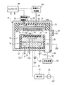
図1に、本発明の一実施形態におけるプラズマ処理装置の構成を示す。このプラズマ処理装置は、カソードカップルの容量結合型(平行平板型)プラズマエッチング装置として構成されており、たとえば表面がアルマイト処理(陽極酸化処理)されたアルミニウムからなる円筒形の真空チャンバ(処理容器)10を有している。チャンバ10は保安接地されている。
FIG. 1 shows the configuration of a plasma processing apparatus according to an embodiment of the present invention. This plasma processing apparatus is configured as a cathode-coupled capacitively coupled (parallel plate type) plasma etching apparatus. For example, a cylindrical vacuum chamber (processing vessel) made of aluminum whose surface is anodized (anodized). 10. The
チャンバ10の底部には、セラミックなどの絶縁板12を介して円柱状のサセプタ支持台14が配置され、このサセプタ支持台14の上にたとえばアルミニウムからなるサセプタ16が設けられている。サセプタ16は下部電極を構成し、この上に被処理基板としてたとえば半導体ウエハWが載置される。
A
サセプタ16の上面には半導体ウエハWを静電吸着力で保持するための静電チャック18が設けられている。この静電チャック18は導電膜からなる電極20を一対の絶縁層または絶縁シートの間に挟み込んだものであり、電極20には直流電源22が電気的に接続されている。直流電源22からの直流電圧により、半導体ウエハWをクーロン力で静電チャック18に吸着保持できるようになっている。静電チャック18の周囲でサセプタ16の上面には、エッチングの均一性を向上させるためのたとえばシリコンからなるフォーカスリング24が配置されている。サセプタ16およびサセプタ支持台14の側面にはたとえば石英からなる円筒状の内壁部材25が貼り付けられている。
An
サセプタ支持台14の内部には、たとえば円周方向に延びる冷媒室26が設けられている。この冷媒室26には、外付けのチラーユニット(図示せず)より配管27a,27bを介して所定温度の冷媒たとえば冷却水が循環供給される。冷媒の温度によってサセプタ16上の半導体ウエハWの処理温度を制御できるようになっている。さらに、伝熱ガス供給機構(図示せず)からの伝熱ガスたとえばHeガスが、ガス供給ライン28を介して静電チャック18の上面と半導体ウエハWの裏面との間に供給される。
Inside the susceptor support 14, for example, a
サセプタ16には、プラズマ生成用の高周波電源30が整合器32および給電棒33を介して電気的に接続されている。この高周波電源30は、チャンバ10内でプラズマ処理を行う際に所定の高周波数たとえば40MHzの高周波をサセプタ16に印加する。
A high
サセプタ16の上方には、このサセプタと平行に対向して上部電極34が設けられている。この上部電極34は、多数のガス噴出孔36aを有するたとえばSi、SiCなどの半導体材料からなる電極板36と、この電極板36を着脱可能に支持する導電材料たとえば表面がアルマイト処理されたアルミニウムからなる電極支持体38とで構成されており、チャンバ10にリング状の絶縁体35を介して電気的に浮いた状態で取り付けられている。この上部電極34とサセプタ16とチャンバ10の側壁とでプラズマ生成空間または処理空間PSが形成されている。
An
リング状絶縁体35は、たとえばアルミナ(Al2O3)からなり、上部電極34の外周面とチャンバ10の側壁との間の隙間を気密に塞ぐように取り付けられ、上部電極34を物理的に支持するとともに、上部電極34とチャンバ10との間の静電容量の一部を構成している。
The ring-shaped
電極支持体38は、その内部にガスバッファ室40を有するとともに、その下面にガスバッファ室40から電極板36のガス噴出孔36aに連通する多数のガス通気孔38aを有している。ガスバッファ室40にはガス供給管42を介して処理ガス供給部44が接続されている。処理ガス供給部44より所定の処理ガスがガスバッファ室40に導入されると、電極板36のガス噴出孔36aよりサセプタ16上の半導体ウエハWに向けて処理空間PSに処理ガスがシャワー状に噴出されるようになっている。このように、上部電極34は、処理空間PSに処理ガスを供給するためのシャワーヘッドを兼ねている。
The
また、電極支持体38の内部には冷媒たとえば冷却水を流す通路(図示せず)も設けられており、外部のチラーユニットにより冷媒を介して上部電極34の全体、特に電極板36を所定温度に温調するようになっている。さらに、上部電極34に対する温度制御をより安定化させるために、電極支持体38の内部または上面にたとえば抵抗発熱素子からなるヒータ(図示せず)を取り付ける構成も可能である。
Further, a passage (not shown) through which a coolant such as cooling water flows is provided inside the
上部電極34の上面とチャンバ10の天井との間には適当なギャップサイズの隙間が設けられ、そこに空間50が形成されている。この空間50は、大気空間でもよいが、好ましくは真空空間として構成され、上部電極34をチャンバ10ないし周囲温度から熱的に遮断するだけでなく、ガスの排除によって上部電極34とチャンバ10との間の放電を防止する機能も有している。このように空間50を真空にする場合は、処理空間PSとは別個に真空排気し、気密構造によって真空状態を保持する。この実施形態では、放電防止機能をさらに高めるために、空間50の内壁の全部または一部(図示の例は上面のみ)をシート状の絶縁体52で覆っている。この絶縁体52には耐熱性に優れたポリイミド系の樹脂を好適に使用することができるが、テフロン(登録商標)や石英等でもよい。
A gap having an appropriate gap size is provided between the upper surface of the
サセプタ16およびサセプタ支持台14とチャンバ10の側壁との間に形成される環状の空間は排気空間となっており、この排気空間の底にはチャンバ10の排気口54が設けられている。この排気口54に排気管56を介して排気装置58が接続されている。排気装置58は、ターボ分子ポンプなどの真空ポンプを有しており、チャンバ10の室内、特に処理空間PSを所望の真空度まで減圧できるようになっている。また、チャンバ10の側壁には半導体ウエハWの搬入出口60を開閉するゲートバルブ62が取り付けられている。
An annular space formed between the susceptor 16 and the
このプラズマエッチング装置は、空間50内に容量可変の可変コンデンサ86を設けており、チャンバ10の外たとえば上面に備え付けの静電容量制御部85により可変コンデンサ86の容量を可変するようにしている。
In this plasma etching apparatus, a
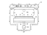
ここで、図2および図3に可変コンデンサ86の構成例を示す。この可変コンデンサ86は、上部電極34の上面に接触または近接する第1の位置と上部電極34から上方に離れた第2の位置との間で移動可能な導体板88と、この導体板88を上下に移動または変位させるための操作機構たとえば操作棒90とを有する。ここで、導体板88と上部電極34との間にコンデンサが形成される。導体板88の面積が大きいほど、容量可変の感度または範囲を大きくすることができる。図2の操作機構90は、導電性の材質、または高周波に対して導電性の性質を持つ材質、または高周波に対して低インピーダンスの材質からなり、直接あるいはチャンバ10を介して接地される。図3の操作機構90は絶縁性の材質でもよい。静電容量制御部85は、たとえば回転量を任意に制御できるステップモータと、このステップモータの回転駆動軸の回転を操作機構90の直進(昇降)運動に変換する運動変換機構(たとえばボールネジ機構)等を有しており、導体板88の高さ位置の可変制御を通じて可変コンデンサ86の容量を連続的に可変できるようになっている。導体板88をチャンバ10の天井面に近づければ近づけるほど、上部電極34の接地容量を小さくすることができる。反対に、導体板88を上部電極34の上面に近づければ近づけるほど、上部電極34の接地容量を大きくすることができる。極端には上部電極34に導体板88を接触させて上部電極34を接地し、接地容量を無限大にすることもできる。
Here, FIG. 2 and FIG. 3 show a configuration example of the
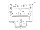
図4に、別の実施例による静電容量可変部85の構成を示す。この実施例は、上部電極34とチャンバ10の側壁との間に設けられるリング状絶縁体35の中に環状の液体収容室94を形成し、配管92を介してチャンバ10の外から適当な誘電率を有する液体(たとえばガルデンのような有機溶剤)Qを出し入れできる構成としている。誘電性液体Qの種類(誘電率)または液量を変えることでリング状絶縁体35全体の静電容量ひいては上部電極34の接地容量を可変することができる。
FIG. 4 shows a configuration of the
なお、静電容量制御部85には、このプラズマ処理装置内の各部の動作および装置全体のシーケンスを制御するコントローラ96より可変コンデンサ86の容量(目標値)を指示する制御信号が与えられる。
The electrostatic
このプラズマエッチング装置において、エッチングを行なうには、先ずゲートバルブ62を開状態にして加工対象の半導体ウエハWをチャンバ10内に搬入して、静電チャック18の上に載置する。そして、処理ガス供給部44より処理ガスつまりエッチングガス(一般に混合ガス)を所定の流量および流量比でチャンバ10内に導入し、排気装置58による真空排気でチャンバ10内の圧力を設定値にする。さらに、高周波電源30より所定のパワーで高周波(40MHz)をサセプタ16に印加する。また、直流電源22より直流電圧を静電チャック18の電極20に印加して、半導体ウエハWを静電チャック18上に固定する。上部電極34のシャワーヘッドより吐出されたエッチングガスは処理空間PSで高周波の放電によってプラズマ化し、このプラズマで生成されるラジカルやイオンによって半導体ウエハWの主面の膜がエッチングされる。
In order to perform etching in this plasma etching apparatus, first, the
この容量結合型プラズマエッチング装置は、サセプタ(下部電極)16に40MHzあるいはそれ以上の高周波を印加することにより、プラズマを好ましい解離状態で高密度化し、より低圧の条件下でも高密度プラズマを形成することができる。しかも、カソードカップル方式であり、サセプタ16に生じる自己バイアス電圧を利用してプラズマ中のイオンをウエハWにほぼ垂直に引き込んで、異方性のエッチングを行える。
In this capacitively coupled plasma etching apparatus, by applying a high frequency of 40 MHz or higher to the susceptor (lower electrode) 16, the plasma is densified in a preferable dissociation state, and high-density plasma is formed even under lower pressure conditions. be able to. In addition, it is a cathode-coupled method, and anisotropic etching can be performed by drawing ions in the plasma almost perpendicularly to the wafer W by using a self-bias voltage generated in the
また、プラズマ生成に適した比較的高い周波数(たとえば40MHz)の第1高周波とイオン引き込みに適した比較的低い周波数(たとえば2MHz)の第2高周波とを下部電極に重畳して印加する下部2周波重畳印加方式も可能である。この場合の装置構成としては、たとえば図5に示すように、サセプタ16に第2高周波を給電するための高周波電源64、整合器66および給電棒68を増設すればよい。このような下部2周波重畳印加方式においては、処理空間PSで生成するプラズマの密度を第1高周波(40MHz)により最適化し、サセプタ16に生じる自己バイアス電圧またはイオンシースを第2高周波(2MHz)により最適化することができ、より選択性の高い異方性エッチングが可能となる。
Further, the lower two frequencies are applied by superposing the first high frequency with a relatively high frequency (for example, 40 MHz) suitable for plasma generation and the second high frequency with a relatively low frequency (for example, 2 MHz) suitable for ion attraction on the lower electrode. A superimposed application method is also possible. As an apparatus configuration in this case, for example, as shown in FIG. 5, a high
次に、このプラズマエッチング装置における可変コンデンサ(静電容量可変部)86の作用を説明する。図6および図7において、上部電極34は電気的には可変コンデンサ86および固定コンデンサまたはキャパシタ70,72を介して接地電位のチャンバ10に接続(接地)される。ここで、キャパシタ70は、上部電極34とチャンバ10の側壁との間の容量(固定容量)であり、主としてリング状絶縁体35によって与えられる。一方、キャパシタ72は、可変コンデンサ86と並列に上部電極34とチャンバ10の天井との間に存在する容量(固定容量)である。上部電極34の周囲の静電容量または接地容量は、可変コンデンサ86の容量とキャパシタ70,72の容量とを足し合わせた合成容量として与えられる。
Next, the operation of the variable capacitor (capacitance variable portion) 86 in this plasma etching apparatus will be described. 6 and 7, the
先ず、可変コンデンサ86の容量を高めに調節して、上部電極34の接地容量(合成容量)をたとえば20000pF以上に選んだ場合(極端には導体板88を上部電極板34に接触させて無限大の容量値とした場合)の作用を説明する。この場合は、図6に示すように、高周波電源30からの高周波がサセプタ16に印加されると、サセプタ16と上部電極34との間の高周波放電およびサセプタ16とチャンバ10の側壁との間の高周波放電によって処理空間PS内で処理ガスのプラズマが生成し、生成したプラズマは四方に、特に上方および半径方向外側に拡散し、プラズマ中の電子電流は上部電極34やチャンバ10の側壁等を通ってグランドへ流れる。ここで、サセプタ16においては高周波の周波数が高くなるほど表皮効果によってサセプタ中心部に高周波電流が集まりやすく、しかも真向かいの上部電極34が高容量つまり低インピーダンスを介して接地されているため、プラズマ中の電子電流の中でチャンバ10の側壁へ流れる割合はかなり低く、大部分は上部電極34に、しかもその中心部に流れる。その結果、プラズマ密度の空間分布特性は、電極中心部が最も高くて半径方向外側の周辺部にいくほど低くなるような山形のプロファイルになりやすい。しかし、一方で、上部電極34に高周波電流または電子電流が多く流れることによって、上部電極34において自己バイアスによるイオンの入射量が増大してスパッタ効果が強まるという一面もある。
First, when the capacitance of the
これに対して、可変コンデンサ86の容量を低めに調節して、上部電極34の接地容量(合成容量)をたとえば250pF以下に選んだ場合は、図7に示すように処理空間PS内のプラズマ分布は半径方向外側に拡張する。この場合も、高周波電源30より高周波がサセプタ16に印加されると、サセプタ16と上部電極34との間の高周波放電およびサセプタ16とチャンバ10の側壁との間の高周波放電によって処理空間PS内でエッチングガスのプラズマが生成し、生成したプラズマは上方および半径方向外側に拡散し、プラズマ中の電子電流は上部電極34やチャンバ10の側壁等を通ってグランドへ流れる。そして、サセプタ16においてはサセプタ中心部に高周波電流が集まりやすいのも、図6の場合と同じである。しかし、上部電極34の接地容量またはインピーダンスが低いため、サセプタ16の中心部に高周波電流が集まってもそこから真向かいの上部電極34へは流れにくくなる。このため、プラズマ中の電子電流の中でチャンバ10の側壁へ流れる割合は決して低くはなく、接地容量の値次第で、つまり可変コンデンサ86の容量値次第で、サセプタ16と上部電極34との間およびサセプタ16とチャンバ10の側壁との間でそれぞれ流れる電子電流の比を任意に制御することができる。一方で、上部電極34に流れる高周波電流または電子電流が少なくなると、上部電極34におけるイオン入射量ないしスパッタ効果が低下するという一面もある。
On the other hand, when the capacitance of the
この実施形態のプラズマエッチング装置は、上記のように静電容量可変部86の静電容量を可変できる構成を有し、プロセス条件に応じて上部電極34の接地容量を適宜切り替えて、特に高容量接地(低インピーダンス)モードあるいは低容量接地(高インピーダンス)モードのいずれかを選択することにより、後述するメモリー効果の防止ないし低減とプロセス均一性とのバランスまたはトレードオフを最適化してプロセス全体の加工性を向上させることができる。
The plasma etching apparatus of this embodiment has a configuration capable of varying the capacitance of the
次に、この実施形態のプラズマエッチング装置における具体的なプラズマエッチング加工の一例を説明する。このエッチング加工は、層間絶縁膜としての有機系low-k膜に接続孔(ビアホール)を形成するものであり、下部2周波重畳印加方式(図5)を用いるものとする。 Next, an example of specific plasma etching processing in the plasma etching apparatus of this embodiment will be described. In this etching process, a connection hole (via hole) is formed in an organic low-k film as an interlayer insulating film, and a lower two-frequency superimposed application method (FIG. 5) is used.
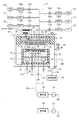
図8に、この実施例における処理ガス供給部44の詳細な構成例を示す。主ガス供給管42には、処理ガス供給系として各種原料ガスの供給源が各専用または分岐ガス供給管を介して接続されている。この実施例では、後述するようにエッチング用混合ガスの原料ガスとしてCF4、CHF3、CH3F、C4F8、Ar、N2の6種類を使用することから、それらの原料ガスを供給するガス供給源100〜110が用意されている。それぞれの専用ガス供給管には、コントローラ96により各々独立的かつ任意に制御可能なマスフローコントローラ(MFC)100a〜110aおよび開閉バルブ100b〜110bが設けられている。
FIG. 8 shows a detailed configuration example of the processing
エッチング加工の対象となる半導体ウエハWの主面上には、図9の(a)に示すように、多層配線構造における下層側配線層112、バリア層114、有機系low-k膜(層間絶縁膜)116およびマスク118が下からこの順に積層されている。配線層112は、たとえばCu配線層であり、たとえばデュアルダマシン加工で形成されている。バリア層114は、たとえば1000Å(0.1μm)の膜厚を有する窒化珪素(SiN)膜であり、たとえばCVD(Chemical Vapor Deposition)法により形成されている。有機系low-k膜116は、たとえば1μmの膜厚を有するSiOC系low-k膜であり、たとえばCVD法により形成されている。マスク118は、レジスト膜であり、通常のフォトリソグラフィによって形成され、ビアホールの孔あけ位置に開口部118aを有している。
On the main surface of the semiconductor wafer W to be etched, as shown in FIG. 9A, the
この実施例では、かかる被処理体の半導体ウエハWに対して3ステップ方式のエッチング加工を行う。先ず、第1ステップとして、デポジションプロセスのエッチングを行う。この第1ステップにおける主なエッチング条件は次のとおりである。
処理ガス:CF4/CH3F/N2=流量50/5/100sccm
チャンバ内の圧力:20mTorr
高周波電力:40MHz/2MHz=1000/0W
In this embodiment, a three-step etching process is performed on the semiconductor wafer W as the object to be processed. First, as a first step, a deposition process is etched. The main etching conditions in this first step are as follows.
Process gas: CF 4 / CH 3 F / N 2 =
Pressure in chamber: 20mTorr
High frequency power: 40MHz / 2MHz = 1000 / 0W
この第1ステップでは、エッチングガスにパーフロロカーボン系のCH3Fを使用する。すると、CH3F中のプラズマで分解されたH分子がすぐにFと反応してHFとして排気されることによってCが残りやすくなる。その結果、カーボン系のデポが多量に発生してレジストマスク118の開口部118aおよび上面に付近に付着し、これが後工程でマスク選択比を高める保護膜となる。しかし、ポリマーが多量に発生することで、しかもサセプタ16に第2高周波(2MHz)を印加しないため(つまり、上部電極34へのイオン入射が弱いため)、上部電極34にデポが付きやすい。
In this first step, perfluorocarbon-based CH 3 F is used as an etching gas. Then, H molecules decomposed by the plasma in CH 3 F immediately react with F and are exhausted as HF, so that C tends to remain. As a result, a large amount of carbon-based deposits are generated and adhere to the
このことから、上部電極34の接地容量については、図6のように可変コンデンサ86の容量を高めに調節して高容量接地(低インピーダンス)モードに切り替え、極端には短絡接地とする。これにより、上部電極34に対するイオンの入射効率を高めてイオンスパッタを促進し、デポ膜が付かないようにすることができる。
Therefore, for the ground capacitance of the
この第1ステップは、図9の(b)に示すように、有機系low-k膜116に形成されるホール116aの底が所定の深さ、たとえば1000Å付近の深さに達したところで、終了する。この第1ステップの終了に際しては、CF4/CH3F/N2の混合ガスの供給を止める、つまり開閉バルブ100b,104b,110bを閉めるとともに、高周波電源30の出力をオフにする。ただし、排気装置58の排気動作はそのまま継続させる。
As shown in FIG. 9B, the first step is terminated when the bottom of the
次に、第2のステップとして、メインエッチングを行う。この第2ステップにおける主なエッチング条件は次のとおりである。
処理ガス:CHF3/CF4/Ar/N2=流量40/30/1000/150sccm
チャンバ内の圧力:30mTorr
高周波電力:40MHz/2MHz=1000/1000W
Next, main etching is performed as a second step. The main etching conditions in the second step are as follows.
Process gas: CHF 3 / CF 4 / Ar / N 2 =
Pressure in the chamber: 30mTorr
High frequency power: 40MHz / 2MHz = 1000 / 1000W
第2ステップでは、化学反応によるプラズマアシストエッチングにイオン照射によるイオンアシストエッチングが重なり合って、高速の異方性エッチングが行われる。その際、上部電極34に先の第1ステップのプロセスで生成されたデポ膜が付いていない状態で第2ステップのプロセスを開始しているので、第1ステップのプロセスの影響を受けることはない。
In the second step, high-speed anisotropic etching is performed by overlapping plasma-assisted etching by chemical reaction with ion-assisted etching by ion irradiation. At this time, since the second step process is started in a state where the deposition film generated in the first step process is not attached to the
もっとも第2ステップのプロセスでも、パーフロロカーボン系のCHF3から多量のポリマーが発生し、第1ステップのときほどではないにしても上部電極34にデポが付きやすく、プロセス時間が比較的長いぶんデポ膜が蓄積して大きく成長する可能性は大きい。
However, even in the second step process, a large amount of polymer is generated from perfluorocarbon-based CHF 3 , and if not as much as in the first step, the
この点に鑑みて、第2ステップにおいても、上部電極34の接地容量を図6のような高容量接地モードとし、極端には短絡接地とする。これにより、上部電極34に対するイオンの入射効率を高めてイオンスパッタを促進し、デポ膜が付かないようにすることができる。
In view of this, in the second step, the ground capacitance of the
第2のステップは、図9の(c)に示すように、有機系low-k膜116のホール116aの底が所定の深さ、たとえば8000Å付近の深さに達したところで、終了する。このステップ終了に際しては、開閉バルブ102b,100b,108b,110bを閉めてCHF3/CF4/Ar/N2混合ガスの供給を止める。同時に、両高周波電源30,64の出力をいったんオフにする。
As shown in FIG. 9C, the second step ends when the bottom of the
次に、最後の第3ステップとして、オーバーエッチングを行う。この第3ステップにおける主なエッチング条件は次のとおりである。
処理ガス:C4F8/Ar/N2=流量6/1000/150sccm
チャンバ内の圧力:50mTorr
高周波電力:40MHz/2MHz=1000/1000W
Next, overetching is performed as the final third step. The main etching conditions in the third step are as follows.
Process gas: C 4 F 8 / Ar / N 2 = flow rate 6/1000/150 sccm
Pressure in the chamber: 50mTorr
High frequency power: 40MHz / 2MHz = 1000 / 1000W
第3ステップでも、ホール116aの異方性(垂直形状)を保ったまま下地膜(窒化珪素)62に達するまで、有機系low-k膜116をエッチングする。この場合にも、上部電極34に先の第2ステップのプロセスで生成されたデポ膜が付いていない状態で第3ステップのプロセスを開始するので、第2ステップのプロセスの影響を受けることはない。
Also in the third step, the organic low-
第3ステップのプロセスでエッチングガスに用いるC4F8/Ar/N2混合ガスは、下地膜(窒化珪素)62に対する選択比が高いという特長があり、フロロカーボンのポリマーを発生するもののその発生量は比較的少なく、しかもこの第3ステップに続く後工程のプロセスがない。つまり、この第3ステップのプロセス中に上部電極34にデポ膜が付いても、そのデポ膜によって次のプロセスが前プロセスの影響を受ける効果(メモリー効果)を考慮しなくて済む。なお、上部電極34やチャンバ10の側壁に付いたデポ膜は、たとえばプラズマクリーニングによって別途除去することができる。
The C 4 F 8 / Ar / N 2 mixed gas used as the etching gas in the third step process has a feature that the selection ratio with respect to the base film (silicon nitride) 62 is high, and generates a fluorocarbon polymer. Is relatively small, and there is no subsequent process following this third step. That is, even if a deposition film is formed on the
この点に鑑みて、第3ステップにおいては、上部電極34の接地容量を図7のような低容量接地(高インピーダンス)モードに切り替える。これにより、サセプタ16と上部電極34との間で流れる電子電流を相対的に減少させるとともにサセプタ16とチャンバ10の側壁との間で流れる電子電流を相対的に増加させ、処理空間PSで生成するプラズマの密度を半径方向外側に拡げることができる。
In view of this, in the third step, switching the ground capacitance of the
この場合、半導体ウエハW上のエッチングレートを空間的に(特に半径方向で)均一化してもよいが、中心部よりもエッジ部のエッチングレートを相対的に高くするのも好ましい。すなわち、先の第1および第2ステップでは、上記のようにメモリー効果防止を重視して上部電極34の接地容量を高めに設定したことから、プラズマ密度は相対的に中心部が高く周辺部が低くなる傾向があり、それによってビアホール形成のエッチングレートも相対的に中心部が高く周辺部が低くなりやすい。結果として、第2ステップの終了時点で、ホール116aの底の深さには空間的に(特に半径方向で)ばらつきがあり、中心部で相対的に深く、エッジ部で相対的に浅くなっている。
In this case, the etching rate on the semiconductor wafer W may be made spatially uniform (particularly in the radial direction), but it is also preferable to make the etching rate at the edge portion relatively higher than the central portion. That is, in the first and second steps, since the grounding capacity of the
そこで、最後の第3ステップで、逆にプラズマ密度を中心部で相対的に低く周辺部で相対的に高くし、半導体ウエハW上のエッチングレートを中心部で相対的に低くエッジ部で相対的に高くすることで、それまでのエッチング深さのばらつきをある程度までキャンセルすることができる。このことによって、第1〜第3ステップを通じたプロセス全体のエッチングレートの面内均一性を向上させることができる。 Therefore, in the final third step, the plasma density is relatively low at the center and relatively high at the periphery, and the etching rate on the semiconductor wafer W is relatively low at the center and relatively low at the edge. By making it high, it is possible to cancel variations in etching depth up to that point to some extent. This can improve the in-plane uniformity of the etching rate of the entire process through the first to third steps.
上記したように、この実施形態によれば、上部電極34の接地容量を可変に構成し、プロセス条件に応じて、たとえば連続するプロセスにおいて前のプロセスが上部電極34にデポ膜を付けやすいときはそのプロセス中は上部電極34の接地容量を高容量接地(低インピーダンス)モードに切り替えて上部電極34にデポ膜を付き難くし、次のプロセスに与える影響またはメモリー効果を防止ないし低減することができる。また、上部電極34にデポ膜が付け難いプロセスや最終工程のプロセスのときは、上部電極34の接地容量を低容量接地(高インピーダンス)モードに切り替えて、処理空間PS内で生成するプラズマの密度を半径方向外側に拡げ、これによってプロセス均一性の向上をはかることができる。
As described above, according to this embodiment, the ground capacitance of the
上記した実施例における有機系low-k膜のビアホールエッチングは一例であり、本発明は任意のマルチステッププロセスに適用可能であり、もちろん単ステップのプロセスにも適用可能である。また、上部電極34に直流電源(図示せず)を電気的に接続して、任意の直流電圧を上部電極34に印加する構成または方式も可能である。この場合も、上部電極34はチャンバ10の電位つまり接地電位からは電気的に浮いた状態で直流的な作用を奏することになる。
The via hole etching of the organic low-k film in the above-described embodiment is an example, and the present invention can be applied to an arbitrary multi-step process, and can be applied to a single-step process. Further, a configuration or a system in which a DC power source (not shown) is electrically connected to the
また、別の実施形態として、ウエハの処理枚数に応じて、静電容量の値を変化させてもよい。一般に、チャンバ内部のパーツの温度がプラズマにより上昇するにつれて、ウエハエッジ部のエッチングレートが低下する傾向にある。そこで、特にエッチング初期では、ウエハ中心のエッチングレートがウエハエッジ部のエッチングレートの上昇に合うように増加させて均一性を保ち、プロセス枚数が進み、ウエハエッジ部のエッチングレートが低下したなら、静電容量可変部の静電容量の値を小さくしてウエハエッジ部でのエッチングレートの低下を低減させる。 In another embodiment, the capacitance value may be changed according to the number of wafers processed. Generally, as the temperature of parts inside the chamber rises due to plasma, the etching rate of the wafer edge portion tends to decrease. Therefore, especially in the initial stage of etching, if the etching rate at the center of the wafer is increased so as to match the increase in the etching rate at the wafer edge portion to maintain uniformity, the number of processes proceeds, and the etching rate at the wafer edge portion decreases. A decrease in the etching rate at the wafer edge portion is reduced by reducing the capacitance value of the variable portion.
上記した実施形態で用いた高周波の周波数は一例であり、プロセスに応じて任意の周波数を使用することが可能である。また、装置内の各部の構成も種々の変形が可能である。特に、上記実施形態における静電容量可変部86の構成は一例であり、上部電極34の周囲の静電容量または接地容量を所望の範囲で可変できる任意のキャパシタ構造を採用することができる。上記実施形態はプラズマエッチング装置およびプラズマエッチング方法に係るものであったが、本発明はプラズマCVD、プラズマ酸化、プラズマ窒化、スパッタリングなどの他のプラズマ処理装置および処理方法にも適用可能である。また、本発明における被処理基板は半導体ウエハに限るものではなく、フラットパネルディスプレイ用の各種基板や、フォトマスク、CD基板、プリント基板等も可能である。
The frequency of the high frequency used in the above embodiment is an example, and an arbitrary frequency can be used depending on the process. In addition, the configuration of each part in the apparatus can be variously modified. In particular, the configuration of the
10 チャンバ(処理容器)
16 サセプタ(下部電極)
30 高周波電源
34 上部電極
35 リング状絶縁体
36 電極板
36a ガス噴出孔
38 電極支持体
40 ガスバッファ室
42 ガス供給管
44 処理ガス供給部
50 空間
52 絶縁体
64 高周波電源
70,72 キャパシタ
85 静電容量制御部
86 可変コンデンサ(静電容量可変部)
10 chamber (processing vessel)
16 Susceptor (lower electrode)
DESCRIPTION OF
Claims (8)
前記第1の電極を前記処理容器に絶縁体または空間を介して取り付けるとともに静電容量可変の可変コンデンサを介して接地電位の部材に電気的に接続して、前記第1の電極と前記処理容器との間に存在するインピーダンスをインダクタンスを含まない常時容量性の可変制御可能なインピーダンスとし、
前記プラズマプロセスが前記第1の電極に堆積膜が付きやすいプロセスであるときは前記可変コンデンサの静電容量を高めの第1のキャパシタンス値に切り替え、前記プラズマプロセスが前記第1の電極に堆積膜が付きにくいプロセスであるときは前記可変コンデンサの静電容量を前記第1のキャパシタンス値よりも低い低めの第2のキャパシタンス値に切り替える、
プラズマ処理方法。 A first electrode and a second electrode are arranged in parallel at a predetermined interval in a vacuumable grounded processing container, and the substrate to be processed is opposed to the first electrode by the second electrode. Supporting, evacuating the inside of the processing vessel to a predetermined pressure, supplying a desired processing gas to a processing space between the first electrode, the second electrode, and the side wall of the processing vessel, and A plasma processing method of applying a first high frequency to two electrodes and performing a desired plasma process on the substrate under plasma generated in the processing space,
Wherein the first electrode is electrically connected to a member of the ground potential via a variable capacitor of the capacitive variable is attached via an insulator or a space in said process vessel, said process vessel and said first electrode The impedance that exists between and is always a capacitive variable controllable impedance that does not include inductance ,
When the plasma process is a process in which a deposited film is easily attached to the first electrode, the capacitance of the variable capacitor is switched to a higher first capacitance value, and the plasma process is performed on the first electrode. When the process is difficult to stick, the capacitance of the variable capacitor is switched to a lower second capacitance value lower than the first capacitance value.
Plasma processing method.
前記第1の電極を前記処理容器に絶縁体または空間を介して取り付けるとともに静電容量可変の可変コンデンサを介して接地電位の部材に電気的に接続して、前記第1の電極と前記処理容器との間に存在するインピーダンスをインダクタンスを含まない常時容量性の可変制御可能なインピーダンスとし、
最後のステップを除く各ステップのプロセスのときは前記可変コンデンサの静電容量を高めの第1のキャパシタンス値に切り替え、最後のステップのプロセスのときは前記可変コンデンサの静電容量を前記第1のキャパシタンス値よりも低い低めの第2のキャパシタンス値に切り替える、
プラズマ処理方法。 A first electrode and a second electrode are arranged in parallel at a predetermined interval in a vacuumable grounded processing container, and the substrate to be processed is opposed to the first electrode by the second electrode. Supporting, evacuating the inside of the processing vessel to a predetermined pressure, supplying a desired processing gas to a processing space between the first electrode, the second electrode, and the side wall of the processing vessel, and A plasma processing method of applying a first high frequency to two electrodes and performing a multi-step plasma process on the substrate under plasma generated in the processing space,
Wherein the first electrode is electrically connected to a member of the ground potential via a variable capacitor of the capacitive variable is attached via an insulator or a space in said process vessel, said process vessel and said first electrode The impedance that exists between and is always a capacitive variable controllable impedance that does not include inductance ,
In the process of each step except the last step, the capacitance of the variable capacitor is switched to a higher first capacitance value. In the process of the last step, the capacitance of the variable capacitor is changed to the first capacitance value. Switch to a lower second capacitance value lower than the capacitance value,
Plasma processing method.
前記処理容器に絶縁体または空間を介して取り付けられる第1の電極と、
前記第1の電極と接地電位の部材との間に電気的に接続される静電容量可変の可変コンデンサと、
前記処理容器内に前記第1の電極と所定の間隔を空けて平行に配置され、前記第1の電極と対向させて被処理基板を支持する第2の電極と、
前記第1の電極と前記第2の電極と前記処理容器の側壁との間の処理空間に所望の処理ガスを供給する処理ガス供給部と、
前記処理空間で前記処理ガスのプラズマを生成するために前記第2の電極に第1の高周波を印加する第1の高周波給電部と、
前記基板に施すプラズマプロセスのプロセス条件に応じて前記可変コンデンサの静電容量の値を切り替える静電容量制御部と
を有し、
前記第1の電極と前記処理容器との間に存在するインピーダンスをインダクタンスを含まない常時容量性の可変制御可能なインピーダンスとし、
前記静電容量制御部が、前記プラズマプロセスが前記第1の電極に堆積膜が付きやすいプロセスであるときは前記可変コンデンサの静電容量を高めの第1のキャパシタンス値に切り替え、前記プラズマプロセスが前記第1の電極に堆積膜が付きにくいプロセスであるときは前記可変コンデンサの静電容量を前記第1のキャパシタンス値よりも低い低めの第2のキャパシタンス値に切り替える、
プラズマ処理装置。 A grounded processing vessel capable of being evacuated;
A first electrode attached to the processing container via an insulator or space;
A variable capacitor having a variable capacitance that is electrically connected between the first electrode and a ground potential member;
A second electrode disposed in parallel with the first electrode in the processing container at a predetermined interval and supporting the substrate to be processed so as to face the first electrode;
A processing gas supply unit that supplies a desired processing gas to a processing space between the first electrode, the second electrode, and a sidewall of the processing container;
A first high-frequency power feeding unit that applies a first high frequency to the second electrode in order to generate plasma of the processing gas in the processing space;
A capacitance control unit that switches a capacitance value of the variable capacitor according to a process condition of a plasma process applied to the substrate;
The impedance existing between the first electrode and the processing container is an always-capacitance variable controllable impedance that does not include an inductance ,
The capacitance control unit switches the capacitance of the variable capacitor to a higher first capacitance value when the plasma process is a process in which a deposited film is easily attached to the first electrode, and the plasma process When it is a process in which a deposited film is not easily attached to the first electrode, the capacitance of the variable capacitor is switched to a lower second capacitance value lower than the first capacitance value.
Plasma processing equipment.
前記処理容器に絶縁体または空間を介して取り付けられる第1の電極と、
前記第1の電極と接地電位との間に電気的に接続される静電容量可変の可変コンデンサと、
前記処理容器内に前記第1の電極と所定の間隔を空けて平行に配置され、前記第1の電極と対向させて被処理基板を支持する第2の電極と、
前記第1の電極と前記第2の電極と前記処理容器の側壁との間の処理空間に所望の処理ガスを供給する処理ガス供給部と、
前記処理空間で前記処理ガスのプラズマを生成するために前記第2の電極に第1の高周波を印加する第1の高周波給電部と、
前記基板に施すマルチステップ方式のプラズマプロセスにおいて各ステップ毎のプロセス条件に応じて前記可変コンデンサの静電容量の値を切り替える静電容量制御部と
を有し、
前記第1の電極と前記処理容器との間に存在するインピーダンスをインダクタンスを含まない常時容量性の可変制御可能なインピーダンスとし、
前記静電容量制御部が、最後のステップを除く各ステップのプロセスのときは前記可変コンデンサの静電容量を高めの第1のキャパシタンス値に切り替え、最後のステップのプロセスのときは前記可変コンデンサの静電容量を前記第1のキャパシタンス値よりも低い低めの第2のキャパシタンス値に切り替える、
プラズマ処理装置。 A grounded processing vessel capable of being evacuated;
A first electrode attached to the processing container via an insulator or space;
A variable capacitor of variable capacitance that is electrically connected between the first electrode and a ground potential;
A second electrode disposed in parallel with the first electrode in the processing container at a predetermined interval and supporting the substrate to be processed so as to face the first electrode;
A processing gas supply unit that supplies a desired processing gas to a processing space between the first electrode, the second electrode, and a sidewall of the processing container;
A first high-frequency power feeding unit that applies a first high frequency to the second electrode in order to generate plasma of the processing gas in the processing space;
A capacitance control unit that switches the value of the capacitance of the variable capacitor in accordance with process conditions for each step in a multi-step plasma process applied to the substrate;
The impedance existing between the first electrode and the processing container is an always-capacitance variable controllable impedance that does not include an inductance ,
The capacitance control unit switches the capacitance of the variable capacitor to a higher first capacitance value in the process of each step except the last step, and changes the capacitance of the variable capacitor in the process of the last step. Switching the capacitance to a lower second capacitance value lower than the first capacitance value;
Plasma processing equipment.
Priority Applications (8)
| Application Number | Priority Date | Filing Date | Title |
|---|---|---|---|
| JP2006092939A JP5116983B2 (en) | 2006-03-30 | 2006-03-30 | Plasma processing method and plasma processing apparatus |
| KR1020070030133A KR100883231B1 (en) | 2006-03-30 | 2007-03-28 | Plasma processing method and plasma processing apparatus |
| TW096111085A TWI447804B (en) | 2006-03-30 | 2007-03-29 | A plasma processing method and a plasma processing apparatus |
| US11/694,126 US7829463B2 (en) | 2006-03-30 | 2007-03-30 | Plasma processing method and plasma processing apparatus |
| CNB2007100913486A CN100565790C (en) | 2006-03-30 | 2007-03-30 | Plasma treatment method and plasma treatment device |
| CN2009101731291A CN101667532B (en) | 2006-03-30 | 2007-03-30 | Plasma processing apparatus |
| CN2009101732006A CN101667533B (en) | 2006-03-30 | 2007-03-30 | Plasma processing method and plasma processing apparatus |
| CN2009101762016A CN101667534B (en) | 2006-03-30 | 2007-03-30 | Plasma processing apparatus and plasma processing method |
Applications Claiming Priority (1)
| Application Number | Priority Date | Filing Date | Title |
|---|---|---|---|
| JP2006092939A JP5116983B2 (en) | 2006-03-30 | 2006-03-30 | Plasma processing method and plasma processing apparatus |
Publications (2)
| Publication Number | Publication Date |
|---|---|
| JP2007266534A JP2007266534A (en) | 2007-10-11 |
| JP5116983B2 true JP5116983B2 (en) | 2013-01-09 |
Family
ID=38639188
Family Applications (1)
| Application Number | Title | Priority Date | Filing Date |
|---|---|---|---|
| JP2006092939A Active JP5116983B2 (en) | 2006-03-30 | 2006-03-30 | Plasma processing method and plasma processing apparatus |
Country Status (4)
| Country | Link |
|---|---|
| JP (1) | JP5116983B2 (en) |
| KR (1) | KR100883231B1 (en) |
| CN (4) | CN101667533B (en) |
| TW (1) | TWI447804B (en) |
Families Citing this family (15)
| Publication number | Priority date | Publication date | Assignee | Title |
|---|---|---|---|---|
| JP5223377B2 (en) | 2008-02-29 | 2013-06-26 | 東京エレクトロン株式会社 | Electrode for plasma processing apparatus, plasma processing apparatus and plasma processing method |
| JP5563860B2 (en) * | 2010-03-26 | 2014-07-30 | 東京エレクトロン株式会社 | Substrate processing method |
| WO2013137414A1 (en) * | 2012-03-16 | 2013-09-19 | 株式会社クリエイティブ テクノロジー | Electrostatic chuck device and method for producing same |
| KR101842124B1 (en) | 2016-05-27 | 2018-03-27 | 세메스 주식회사 | Support unit, Apparatus and method for treating a substrate |
| CN108206153B (en) * | 2016-12-16 | 2021-02-09 | 台湾积体电路制造股份有限公司 | Wafer bearing device and semiconductor equipment |
| US10553404B2 (en) * | 2017-02-01 | 2020-02-04 | Applied Materials, Inc. | Adjustable extended electrode for edge uniformity control |
| JP6937644B2 (en) * | 2017-09-26 | 2021-09-22 | 東京エレクトロン株式会社 | Plasma processing equipment and plasma processing method |
| JP2019075517A (en) * | 2017-10-19 | 2019-05-16 | 東京エレクトロン株式会社 | Processing device and member having diffusion path |
| CN112309807B (en) * | 2019-08-02 | 2022-12-30 | 中微半导体设备(上海)股份有限公司 | Plasma etching equipment |
| JP2021038452A (en) * | 2019-09-05 | 2021-03-11 | 東京エレクトロン株式会社 | Plasma treatment apparatus and control method |
| JP7325294B2 (en) * | 2019-10-17 | 2023-08-14 | 東京エレクトロン株式会社 | Plasma processing apparatus and plasma processing method |
| WO2021157750A1 (en) * | 2020-02-03 | 2021-08-12 | (주)제이디 | Capacitance-type state measuring device using sensor-mounted wafer |
| CN114256046B (en) * | 2020-09-22 | 2024-07-05 | 中微半导体设备(上海)股份有限公司 | Plasma processing device and operating method thereof |
| CN114695042B (en) * | 2020-12-28 | 2025-02-14 | 中微半导体设备(上海)股份有限公司 | Radio frequency adjustment device, plasma processing equipment and radio frequency electric field adjustment method |
| CN118737797B (en) * | 2024-06-21 | 2025-07-25 | 北京北方华创微电子装备有限公司 | Upper electrode structure and semiconductor process equipment |
Family Cites Families (14)
| Publication number | Priority date | Publication date | Assignee | Title |
|---|---|---|---|---|
| US6251792B1 (en) * | 1990-07-31 | 2001-06-26 | Applied Materials, Inc. | Plasma etch processes |
| US6518195B1 (en) * | 1991-06-27 | 2003-02-11 | Applied Materials, Inc. | Plasma reactor using inductive RF coupling, and processes |
| US5494522A (en) * | 1993-03-17 | 1996-02-27 | Tokyo Electron Limited | Plasma process system and method |
| JP4493756B2 (en) * | 1999-08-20 | 2010-06-30 | 東京エレクトロン株式会社 | Plasma processing apparatus and plasma processing method |
| TW449654B (en) * | 1999-08-25 | 2001-08-11 | Fujitsu General Ltd | Air conditioner |
| JP4819244B2 (en) * | 2001-05-15 | 2011-11-24 | 東京エレクトロン株式会社 | Plasma processing equipment |
| JP4584565B2 (en) * | 2002-11-26 | 2010-11-24 | 東京エレクトロン株式会社 | Plasma processing apparatus and plasma processing method |
| JP2004235105A (en) * | 2003-01-31 | 2004-08-19 | Matsushita Electric Works Ltd | Plasma processing apparatus and plasma processing method |
| JP4388287B2 (en) * | 2003-02-12 | 2009-12-24 | 東京エレクトロン株式会社 | Plasma processing apparatus and high-frequency power supply apparatus |
| JP2004305918A (en) * | 2003-04-07 | 2004-11-04 | Sekisui Chem Co Ltd | Plasma processing method and plasma processing apparatus used for the same |
| JP2005332670A (en) * | 2004-05-19 | 2005-12-02 | Sekisui Chem Co Ltd | Normal pressure plasma surface treatment equipment |
| CN102184830B (en) * | 2004-07-30 | 2012-07-25 | 东京毅力科创株式会社 | Plasma processing apparatus and plasma processing method |
| JP4699127B2 (en) * | 2004-07-30 | 2011-06-08 | 東京エレクトロン株式会社 | Plasma processing apparatus and plasma processing method |
| US20060037704A1 (en) * | 2004-07-30 | 2006-02-23 | Tokyo Electron Limited | Plasma Processing apparatus and method |
-
2006
- 2006-03-30 JP JP2006092939A patent/JP5116983B2/en active Active
-
2007
- 2007-03-28 KR KR1020070030133A patent/KR100883231B1/en active Active
- 2007-03-29 TW TW096111085A patent/TWI447804B/en active
- 2007-03-30 CN CN2009101732006A patent/CN101667533B/en not_active Expired - Fee Related
- 2007-03-30 CN CN2009101762016A patent/CN101667534B/en not_active Expired - Fee Related
- 2007-03-30 CN CNB2007100913486A patent/CN100565790C/en not_active Expired - Fee Related
- 2007-03-30 CN CN2009101731291A patent/CN101667532B/en active Active
Also Published As
| Publication number | Publication date |
|---|---|
| CN101667533A (en) | 2010-03-10 |
| TWI447804B (en) | 2014-08-01 |
| TW200802596A (en) | 2008-01-01 |
| CN101667534A (en) | 2010-03-10 |
| CN100565790C (en) | 2009-12-02 |
| KR100883231B1 (en) | 2009-02-10 |
| CN101047112A (en) | 2007-10-03 |
| KR20070098588A (en) | 2007-10-05 |
| CN101667532A (en) | 2010-03-10 |
| JP2007266534A (en) | 2007-10-11 |
| CN101667533B (en) | 2011-06-15 |
| CN101667532B (en) | 2011-07-27 |
| CN101667534B (en) | 2011-07-27 |
Similar Documents
| Publication | Publication Date | Title |
|---|---|---|
| CN101667532B (en) | Plasma processing apparatus | |
| US7829463B2 (en) | Plasma processing method and plasma processing apparatus | |
| CN100517563C (en) | Plasma processing apparatus and plasma processing method | |
| KR102358732B1 (en) | Plasma etching method and plasma etching apparatus | |
| CN1992164B (en) | Plasma etching method | |
| JP5031252B2 (en) | Plasma processing equipment | |
| KR102260339B1 (en) | Semiconductor device manufacturing method | |
| KR101957348B1 (en) | Plasma processing apparatus and plasma processing method | |
| US8129282B2 (en) | Plasma etching method and computer-readable storage medium | |
| JP2009239012A (en) | Plasma processing device and method of plasma etching | |
| JP2014060440A (en) | Gas modulation to control edge exclusion in bevel edge etching plasma chamber | |
| KR20080006457A (en) | Plasma Etching Method and Computer-readable Storage Media | |
| JP2008244233A (en) | Plasma processing equipment | |
| WO2023008025A1 (en) | Etching method, method for manufacturing semiconductor device, etching program, and plasma processing device | |
| JP4278915B2 (en) | Etching method | |
| JP4827567B2 (en) | Plasma etching method and computer-readable storage medium | |
| US20070218699A1 (en) | Plasma etching method and computer-readable storage medium | |
| JP4615290B2 (en) | Plasma etching method | |
| KR20220011582A (en) | Plasma processing method and plasma processing apparatus | |
| JP5064708B2 (en) | Plasma processing equipment | |
| JP7099675B1 (en) | Etching method, semiconductor device manufacturing method, program and plasma processing device | |
| US20070218698A1 (en) | Plasma etching method, plasma etching apparatus, and computer-readable storage medium |
Legal Events
| Date | Code | Title | Description |
|---|---|---|---|
| A621 | Written request for application examination |
Free format text: JAPANESE INTERMEDIATE CODE: A621 Effective date: 20090218 |
|
| A977 | Report on retrieval |
Free format text: JAPANESE INTERMEDIATE CODE: A971007 Effective date: 20090619 |
|
| A131 | Notification of reasons for refusal |
Free format text: JAPANESE INTERMEDIATE CODE: A131 Effective date: 20111108 |
|
| A521 | Request for written amendment filed |
Free format text: JAPANESE INTERMEDIATE CODE: A523 Effective date: 20120106 |
|
| A131 | Notification of reasons for refusal |
Free format text: JAPANESE INTERMEDIATE CODE: A131 Effective date: 20120703 |
|
| A521 | Request for written amendment filed |
Free format text: JAPANESE INTERMEDIATE CODE: A523 Effective date: 20120903 |
|
| TRDD | Decision of grant or rejection written | ||
| A01 | Written decision to grant a patent or to grant a registration (utility model) |
Free format text: JAPANESE INTERMEDIATE CODE: A01 Effective date: 20121016 |
|
| A01 | Written decision to grant a patent or to grant a registration (utility model) |
Free format text: JAPANESE INTERMEDIATE CODE: A01 |
|
| A61 | First payment of annual fees (during grant procedure) |
Free format text: JAPANESE INTERMEDIATE CODE: A61 Effective date: 20121017 |
|
| R150 | Certificate of patent or registration of utility model |
Ref document number: 5116983 Country of ref document: JP Free format text: JAPANESE INTERMEDIATE CODE: R150 Free format text: JAPANESE INTERMEDIATE CODE: R150 |
|
| FPAY | Renewal fee payment (event date is renewal date of database) |
Free format text: PAYMENT UNTIL: 20151026 Year of fee payment: 3 |
|
| R250 | Receipt of annual fees |
Free format text: JAPANESE INTERMEDIATE CODE: R250 |
|
| R250 | Receipt of annual fees |
Free format text: JAPANESE INTERMEDIATE CODE: R250 |
|
| R250 | Receipt of annual fees |
Free format text: JAPANESE INTERMEDIATE CODE: R250 |
|
| R250 | Receipt of annual fees |
Free format text: JAPANESE INTERMEDIATE CODE: R250 |
|
| R250 | Receipt of annual fees |
Free format text: JAPANESE INTERMEDIATE CODE: R250 |
|
| R250 | Receipt of annual fees |
Free format text: JAPANESE INTERMEDIATE CODE: R250 |
|
| R250 | Receipt of annual fees |
Free format text: JAPANESE INTERMEDIATE CODE: R250 |
|
| R250 | Receipt of annual fees |
Free format text: JAPANESE INTERMEDIATE CODE: R250 |