JP5111745B2 - コンデンサ及びその製造方法 - Google Patents
コンデンサ及びその製造方法 Download PDFInfo
- Publication number
- JP5111745B2 JP5111745B2 JP2005243180A JP2005243180A JP5111745B2 JP 5111745 B2 JP5111745 B2 JP 5111745B2 JP 2005243180 A JP2005243180 A JP 2005243180A JP 2005243180 A JP2005243180 A JP 2005243180A JP 5111745 B2 JP5111745 B2 JP 5111745B2
- Authority
- JP
- Japan
- Prior art keywords
- layer
- electrode
- dielectric layer
- opening
- forming
- Prior art date
- Legal status (The legal status is an assumption and is not a legal conclusion. Google has not performed a legal analysis and makes no representation as to the accuracy of the status listed.)
- Active
Links
- 239000003990 capacitor Substances 0.000 title claims description 50
- 238000004519 manufacturing process Methods 0.000 title claims description 19
- 239000000758 substrate Substances 0.000 claims description 39
- 238000000605 extraction Methods 0.000 claims description 18
- 238000005530 etching Methods 0.000 claims description 11
- 239000012535 impurity Substances 0.000 claims description 6
- 239000003960 organic solvent Substances 0.000 claims description 6
- 239000000463 material Substances 0.000 claims description 4
- 230000004888 barrier function Effects 0.000 claims description 3
- 238000009792 diffusion process Methods 0.000 claims description 2
- PXHVJJICTQNCMI-UHFFFAOYSA-N Nickel Chemical compound [Ni] PXHVJJICTQNCMI-UHFFFAOYSA-N 0.000 description 55
- 229910052751 metal Inorganic materials 0.000 description 30
- 239000002184 metal Substances 0.000 description 30
- 229910052759 nickel Inorganic materials 0.000 description 26
- 239000004020 conductor Substances 0.000 description 15
- 238000000034 method Methods 0.000 description 14
- 239000004065 semiconductor Substances 0.000 description 14
- BASFCYQUMIYNBI-UHFFFAOYSA-N platinum Chemical compound [Pt] BASFCYQUMIYNBI-UHFFFAOYSA-N 0.000 description 13
- JRPBQTZRNDNNOP-UHFFFAOYSA-N barium titanate Chemical compound [Ba+2].[Ba+2].[O-][Ti]([O-])([O-])[O-] JRPBQTZRNDNNOP-UHFFFAOYSA-N 0.000 description 11
- 229910002113 barium titanate Inorganic materials 0.000 description 11
- 238000000206 photolithography Methods 0.000 description 7
- 230000015572 biosynthetic process Effects 0.000 description 6
- 239000010931 gold Substances 0.000 description 6
- 229910052697 platinum Inorganic materials 0.000 description 5
- -1 for example Substances 0.000 description 4
- 229920002120 photoresistant polymer Polymers 0.000 description 4
- 238000004544 sputter deposition Methods 0.000 description 4
- KRHYYFGTRYWZRS-UHFFFAOYSA-N Fluorane Chemical compound F KRHYYFGTRYWZRS-UHFFFAOYSA-N 0.000 description 3
- PCHJSUWPFVWCPO-UHFFFAOYSA-N gold Chemical compound [Au] PCHJSUWPFVWCPO-UHFFFAOYSA-N 0.000 description 3
- 229910052737 gold Inorganic materials 0.000 description 3
- 239000012212 insulator Substances 0.000 description 3
- 238000000059 patterning Methods 0.000 description 3
- 238000007747 plating Methods 0.000 description 3
- 229910000679 solder Inorganic materials 0.000 description 3
- RYGMFSIKBFXOCR-UHFFFAOYSA-N Copper Chemical compound [Cu] RYGMFSIKBFXOCR-UHFFFAOYSA-N 0.000 description 2
- 229910021578 Iron(III) chloride Inorganic materials 0.000 description 2
- 239000004642 Polyimide Substances 0.000 description 2
- VYPSYNLAJGMNEJ-UHFFFAOYSA-N Silicium dioxide Chemical compound O=[Si]=O VYPSYNLAJGMNEJ-UHFFFAOYSA-N 0.000 description 2
- XUIMIQQOPSSXEZ-UHFFFAOYSA-N Silicon Chemical compound [Si] XUIMIQQOPSSXEZ-UHFFFAOYSA-N 0.000 description 2
- 229910052802 copper Inorganic materials 0.000 description 2
- 239000010949 copper Substances 0.000 description 2
- 239000013078 crystal Substances 0.000 description 2
- RBTARNINKXHZNM-UHFFFAOYSA-K iron trichloride Chemical compound Cl[Fe](Cl)Cl RBTARNINKXHZNM-UHFFFAOYSA-K 0.000 description 2
- 229920001721 polyimide Polymers 0.000 description 2
- 229910052710 silicon Inorganic materials 0.000 description 2
- 239000010703 silicon Substances 0.000 description 2
- 229910052814 silicon oxide Inorganic materials 0.000 description 2
- 229910004298 SiO 2 Inorganic materials 0.000 description 1
- 230000032683 aging Effects 0.000 description 1
- 229910052782 aluminium Inorganic materials 0.000 description 1
- XAGFODPZIPBFFR-UHFFFAOYSA-N aluminium Chemical compound [Al] XAGFODPZIPBFFR-UHFFFAOYSA-N 0.000 description 1
- 238000004380 ashing Methods 0.000 description 1
- 230000015556 catabolic process Effects 0.000 description 1
- 230000007797 corrosion Effects 0.000 description 1
- 238000005260 corrosion Methods 0.000 description 1
- 230000003247 decreasing effect Effects 0.000 description 1
- 230000007547 defect Effects 0.000 description 1
- 238000000151 deposition Methods 0.000 description 1
- 239000000428 dust Substances 0.000 description 1
- 238000005516 engineering process Methods 0.000 description 1
- 239000000945 filler Substances 0.000 description 1
- 238000012986 modification Methods 0.000 description 1
- 230000004048 modification Effects 0.000 description 1
- QPJSUIGXIBEQAC-UHFFFAOYSA-N n-(2,4-dichloro-5-propan-2-yloxyphenyl)acetamide Chemical compound CC(C)OC1=CC(NC(C)=O)=C(Cl)C=C1Cl QPJSUIGXIBEQAC-UHFFFAOYSA-N 0.000 description 1
- 230000003647 oxidation Effects 0.000 description 1
- 238000007254 oxidation reaction Methods 0.000 description 1
- 239000011347 resin Substances 0.000 description 1
- 229920005989 resin Polymers 0.000 description 1
- 238000007788 roughening Methods 0.000 description 1
- 238000004528 spin coating Methods 0.000 description 1
- WFKWXMTUELFFGS-UHFFFAOYSA-N tungsten Chemical compound [W] WFKWXMTUELFFGS-UHFFFAOYSA-N 0.000 description 1
- 229910052721 tungsten Inorganic materials 0.000 description 1
- 239000010937 tungsten Substances 0.000 description 1
Images


Classifications
-
- H—ELECTRICITY
- H01—ELECTRIC ELEMENTS
- H01L—SEMICONDUCTOR DEVICES NOT COVERED BY CLASS H10
- H01L23/00—Details of semiconductor or other solid state devices
- H01L23/48—Arrangements for conducting electric current to or from the solid state body in operation, e.g. leads, terminal arrangements ; Selection of materials therefor
- H01L23/50—Arrangements for conducting electric current to or from the solid state body in operation, e.g. leads, terminal arrangements ; Selection of materials therefor for integrated circuit devices, e.g. power bus, number of leads
-
- H—ELECTRICITY
- H01—ELECTRIC ELEMENTS
- H01G—CAPACITORS; CAPACITORS, RECTIFIERS, DETECTORS, SWITCHING DEVICES OR LIGHT-SENSITIVE DEVICES, OF THE ELECTROLYTIC TYPE
- H01G4/00—Fixed capacitors; Processes of their manufacture
- H01G4/002—Details
- H01G4/228—Terminals
-
- H—ELECTRICITY
- H01—ELECTRIC ELEMENTS
- H01G—CAPACITORS; CAPACITORS, RECTIFIERS, DETECTORS, SWITCHING DEVICES OR LIGHT-SENSITIVE DEVICES, OF THE ELECTROLYTIC TYPE
- H01G4/00—Fixed capacitors; Processes of their manufacture
- H01G4/33—Thin- or thick-film capacitors
-
- H—ELECTRICITY
- H01—ELECTRIC ELEMENTS
- H01L—SEMICONDUCTOR DEVICES NOT COVERED BY CLASS H10
- H01L24/00—Arrangements for connecting or disconnecting semiconductor or solid-state bodies; Methods or apparatus related thereto
- H01L24/80—Methods for connecting semiconductor or other solid state bodies using means for bonding being attached to, or being formed on, the surface to be connected
- H01L24/81—Methods for connecting semiconductor or other solid state bodies using means for bonding being attached to, or being formed on, the surface to be connected using a bump connector
-
- H—ELECTRICITY
- H05—ELECTRIC TECHNIQUES NOT OTHERWISE PROVIDED FOR
- H05K—PRINTED CIRCUITS; CASINGS OR CONSTRUCTIONAL DETAILS OF ELECTRIC APPARATUS; MANUFACTURE OF ASSEMBLAGES OF ELECTRICAL COMPONENTS
- H05K1/00—Printed circuits
- H05K1/16—Printed circuits incorporating printed electric components, e.g. printed resistor, capacitor, inductor
- H05K1/162—Printed circuits incorporating printed electric components, e.g. printed resistor, capacitor, inductor incorporating printed capacitors
-
- H—ELECTRICITY
- H01—ELECTRIC ELEMENTS
- H01L—SEMICONDUCTOR DEVICES NOT COVERED BY CLASS H10
- H01L2224/00—Indexing scheme for arrangements for connecting or disconnecting semiconductor or solid-state bodies and methods related thereto as covered by H01L24/00
- H01L2224/80—Methods for connecting semiconductor or other solid state bodies using means for bonding being attached to, or being formed on, the surface to be connected
- H01L2224/81—Methods for connecting semiconductor or other solid state bodies using means for bonding being attached to, or being formed on, the surface to be connected using a bump connector
- H01L2224/818—Bonding techniques
- H01L2224/81801—Soldering or alloying
-
- H—ELECTRICITY
- H01—ELECTRIC ELEMENTS
- H01L—SEMICONDUCTOR DEVICES NOT COVERED BY CLASS H10
- H01L23/00—Details of semiconductor or other solid state devices
- H01L23/48—Arrangements for conducting electric current to or from the solid state body in operation, e.g. leads, terminal arrangements ; Selection of materials therefor
- H01L23/481—Internal lead connections, e.g. via connections, feedthrough structures
-
- H—ELECTRICITY
- H01—ELECTRIC ELEMENTS
- H01L—SEMICONDUCTOR DEVICES NOT COVERED BY CLASS H10
- H01L2924/00—Indexing scheme for arrangements or methods for connecting or disconnecting semiconductor or solid-state bodies as covered by H01L24/00
- H01L2924/01—Chemical elements
- H01L2924/01005—Boron [B]
-
- H—ELECTRICITY
- H01—ELECTRIC ELEMENTS
- H01L—SEMICONDUCTOR DEVICES NOT COVERED BY CLASS H10
- H01L2924/00—Indexing scheme for arrangements or methods for connecting or disconnecting semiconductor or solid-state bodies as covered by H01L24/00
- H01L2924/01—Chemical elements
- H01L2924/01006—Carbon [C]
-
- H—ELECTRICITY
- H01—ELECTRIC ELEMENTS
- H01L—SEMICONDUCTOR DEVICES NOT COVERED BY CLASS H10
- H01L2924/00—Indexing scheme for arrangements or methods for connecting or disconnecting semiconductor or solid-state bodies as covered by H01L24/00
- H01L2924/01—Chemical elements
- H01L2924/01013—Aluminum [Al]
-
- H—ELECTRICITY
- H01—ELECTRIC ELEMENTS
- H01L—SEMICONDUCTOR DEVICES NOT COVERED BY CLASS H10
- H01L2924/00—Indexing scheme for arrangements or methods for connecting or disconnecting semiconductor or solid-state bodies as covered by H01L24/00
- H01L2924/01—Chemical elements
- H01L2924/01029—Copper [Cu]
-
- H—ELECTRICITY
- H01—ELECTRIC ELEMENTS
- H01L—SEMICONDUCTOR DEVICES NOT COVERED BY CLASS H10
- H01L2924/00—Indexing scheme for arrangements or methods for connecting or disconnecting semiconductor or solid-state bodies as covered by H01L24/00
- H01L2924/01—Chemical elements
- H01L2924/01033—Arsenic [As]
-
- H—ELECTRICITY
- H01—ELECTRIC ELEMENTS
- H01L—SEMICONDUCTOR DEVICES NOT COVERED BY CLASS H10
- H01L2924/00—Indexing scheme for arrangements or methods for connecting or disconnecting semiconductor or solid-state bodies as covered by H01L24/00
- H01L2924/01—Chemical elements
- H01L2924/01056—Barium [Ba]
-
- H—ELECTRICITY
- H01—ELECTRIC ELEMENTS
- H01L—SEMICONDUCTOR DEVICES NOT COVERED BY CLASS H10
- H01L2924/00—Indexing scheme for arrangements or methods for connecting or disconnecting semiconductor or solid-state bodies as covered by H01L24/00
- H01L2924/01—Chemical elements
- H01L2924/01072—Hafnium [Hf]
-
- H—ELECTRICITY
- H01—ELECTRIC ELEMENTS
- H01L—SEMICONDUCTOR DEVICES NOT COVERED BY CLASS H10
- H01L2924/00—Indexing scheme for arrangements or methods for connecting or disconnecting semiconductor or solid-state bodies as covered by H01L24/00
- H01L2924/01—Chemical elements
- H01L2924/01074—Tungsten [W]
-
- H—ELECTRICITY
- H01—ELECTRIC ELEMENTS
- H01L—SEMICONDUCTOR DEVICES NOT COVERED BY CLASS H10
- H01L2924/00—Indexing scheme for arrangements or methods for connecting or disconnecting semiconductor or solid-state bodies as covered by H01L24/00
- H01L2924/01—Chemical elements
- H01L2924/01078—Platinum [Pt]
-
- H—ELECTRICITY
- H01—ELECTRIC ELEMENTS
- H01L—SEMICONDUCTOR DEVICES NOT COVERED BY CLASS H10
- H01L2924/00—Indexing scheme for arrangements or methods for connecting or disconnecting semiconductor or solid-state bodies as covered by H01L24/00
- H01L2924/01—Chemical elements
- H01L2924/01079—Gold [Au]
-
- H—ELECTRICITY
- H01—ELECTRIC ELEMENTS
- H01L—SEMICONDUCTOR DEVICES NOT COVERED BY CLASS H10
- H01L2924/00—Indexing scheme for arrangements or methods for connecting or disconnecting semiconductor or solid-state bodies as covered by H01L24/00
- H01L2924/01—Chemical elements
- H01L2924/01082—Lead [Pb]
-
- H—ELECTRICITY
- H01—ELECTRIC ELEMENTS
- H01L—SEMICONDUCTOR DEVICES NOT COVERED BY CLASS H10
- H01L2924/00—Indexing scheme for arrangements or methods for connecting or disconnecting semiconductor or solid-state bodies as covered by H01L24/00
- H01L2924/013—Alloys
- H01L2924/014—Solder alloys
-
- H—ELECTRICITY
- H01—ELECTRIC ELEMENTS
- H01L—SEMICONDUCTOR DEVICES NOT COVERED BY CLASS H10
- H01L2924/00—Indexing scheme for arrangements or methods for connecting or disconnecting semiconductor or solid-state bodies as covered by H01L24/00
- H01L2924/10—Details of semiconductor or other solid state devices to be connected
- H01L2924/11—Device type
- H01L2924/14—Integrated circuits
-
- H—ELECTRICITY
- H01—ELECTRIC ELEMENTS
- H01L—SEMICONDUCTOR DEVICES NOT COVERED BY CLASS H10
- H01L2924/00—Indexing scheme for arrangements or methods for connecting or disconnecting semiconductor or solid-state bodies as covered by H01L24/00
- H01L2924/19—Details of hybrid assemblies other than the semiconductor or other solid state devices to be connected
- H01L2924/1901—Structure
- H01L2924/1904—Component type
- H01L2924/19041—Component type being a capacitor
-
- H—ELECTRICITY
- H01—ELECTRIC ELEMENTS
- H01L—SEMICONDUCTOR DEVICES NOT COVERED BY CLASS H10
- H01L2924/00—Indexing scheme for arrangements or methods for connecting or disconnecting semiconductor or solid-state bodies as covered by H01L24/00
- H01L2924/30—Technical effects
- H01L2924/301—Electrical effects
- H01L2924/30105—Capacitance
-
- H—ELECTRICITY
- H05—ELECTRIC TECHNIQUES NOT OTHERWISE PROVIDED FOR
- H05K—PRINTED CIRCUITS; CASINGS OR CONSTRUCTIONAL DETAILS OF ELECTRIC APPARATUS; MANUFACTURE OF ASSEMBLAGES OF ELECTRICAL COMPONENTS
- H05K2201/00—Indexing scheme relating to printed circuits covered by H05K1/00
- H05K2201/09—Shape and layout
- H05K2201/09209—Shape and layout details of conductors
- H05K2201/095—Conductive through-holes or vias
- H05K2201/09509—Blind vias, i.e. vias having one side closed
-
- H—ELECTRICITY
- H05—ELECTRIC TECHNIQUES NOT OTHERWISE PROVIDED FOR
- H05K—PRINTED CIRCUITS; CASINGS OR CONSTRUCTIONAL DETAILS OF ELECTRIC APPARATUS; MANUFACTURE OF ASSEMBLAGES OF ELECTRICAL COMPONENTS
- H05K2201/00—Indexing scheme relating to printed circuits covered by H05K1/00
- H05K2201/09—Shape and layout
- H05K2201/09209—Shape and layout details of conductors
- H05K2201/095—Conductive through-holes or vias
- H05K2201/096—Vertically aligned vias, holes or stacked vias
-
- H—ELECTRICITY
- H05—ELECTRIC TECHNIQUES NOT OTHERWISE PROVIDED FOR
- H05K—PRINTED CIRCUITS; CASINGS OR CONSTRUCTIONAL DETAILS OF ELECTRIC APPARATUS; MANUFACTURE OF ASSEMBLAGES OF ELECTRICAL COMPONENTS
- H05K2201/00—Indexing scheme relating to printed circuits covered by H05K1/00
- H05K2201/10—Details of components or other objects attached to or integrated in a printed circuit board
- H05K2201/10227—Other objects, e.g. metallic pieces
- H05K2201/10378—Interposers
-
- H—ELECTRICITY
- H05—ELECTRIC TECHNIQUES NOT OTHERWISE PROVIDED FOR
- H05K—PRINTED CIRCUITS; CASINGS OR CONSTRUCTIONAL DETAILS OF ELECTRIC APPARATUS; MANUFACTURE OF ASSEMBLAGES OF ELECTRICAL COMPONENTS
- H05K3/00—Apparatus or processes for manufacturing printed circuits
- H05K3/0011—Working of insulating substrates or insulating layers
- H05K3/0017—Etching of the substrate by chemical or physical means
- H05K3/002—Etching of the substrate by chemical or physical means by liquid chemical etching
Description
このような原因により、特許文献1に開示された技術では、誘電体層の品質が劣化し、漏れ電流の発生、誘電損失の増加、静電容量の低下、経年劣化が早くなる等、製造されるコンデンサの品質が低下する問題がある。
基板と、
前記基板の一方の主面に形成された下部電極と、
前記基板の一方の主面に、前記下部電極から絶縁されて形成された引き出し電極層と、
少なくとも前記下部電極を覆うように形成され、前記下部電極を覆う領域とは異なる領域であって前記引き出し電極層の上に形成された開口部を備える誘電体層と、
少なくとも一部が前記誘電体層を介して前記下部電極と対向するように前記誘電体層上に形成された上部電極と、
前記基板の前記引き出し電極層に対応する位置に形成され、前記基板の一方の主面から他方の主面まで接続するコンタクトホールと、を備え、
前記上部電極は、前記誘電体層上に形成され、前記誘電体層の前記開口部と平面視して重なるように形成された開口部を備える第1の層と、該第1の層上及び前記誘電体層の前記開口部の内壁及び該第1の層の該開口部の内壁及び前記誘電体層の前記開口部を介して露出する前記引き出し電極層とを覆うように形成された第2の層と、を備え、
前記第1の層と前記第2の層とは異なる材料から形成され、
前記上部電極の前記第2の層の上に絶縁層が形成されることを特徴とする。
前記誘電体層の前記開口部は、該電極パッドが形成された領域に平面視して重なるように形成されてもよい。
基板の一方の主面上に下部電極を形成する下部電極形成工程と、
前記基板の一方の主面上に引き出し電極層を形成する引き出し電極層形成工程と、
少なくとも前記下部電極を覆うように誘電体層を形成する誘電体層形成工程と、
少なくとも一部が前記誘電体層を介して前記下部電極と対向するように前記誘電体層上に上部電極の第1の層を形成する第1の層形成工程と、
前記第1の層のうち前記誘電体層を介して前記下部電極と対向しない領域であって前記引き出し電極層に対向する領域に開口部を形成する開口部形成工程と、
前記第1の層をマスクとして用いて、前記第1の層の開口部を介して前記引き出し電極層の上の前記誘電体層に開口部を形成する誘電体層開口部形成工程と、
前記上部電極の第1の層上、前記第1の層の開口部の内壁及び前記誘電体層の前記開口部の内壁及び前記誘電体層の前記開口部の底面を覆うように、前記上部電極の第2の層を形成する第2の層形成工程と、
前記上部電極の前記第2の層の上に絶縁層を形成する絶縁層形成工程と、
前記基板の前記引き出し電極層に対応する位置に、前記基板の一方の主面から他方の主面まで接続するコンタクトホールを形成するコンタクトホール形成工程と、
を備えることを特徴とする。
前記上部電極の前記第1の層を、前記誘電体層内に該レジストパターンに含まれる不純物が拡散することを防ぐバリアとして機能させてもよい。
前記絶縁層形成工程では、前記第2の層により前記誘電体層を有機溶剤又は現像液から保護してもよい。
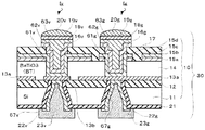
図1は、インターポーザ30の断面構成を示すもので、図3に示す平面図のI−I線での断面に相当する。図示するように、インターポーザ30は、コンデンサ10と、引出用電極層13bと、配線16v、16gと、絶縁膜17と、電極パッド18g、18vと、金属層19g、19vと、バンプ20g、20vと、絶縁層21と、金属層22g、22vと、電極パッド23g、23vと、を備える。コンデンサ10は、基板11と、酸化膜12と、下部(下層)電極13aと、誘電体層14と、上部電極15a〜15dと、から構成される。
金属膜16vは、誘電体層14の開口部61v及び上部電極15aの開口部62vを覆うように形成された上部電極15bと、絶縁膜17の開口部63vと、開口部63v近傍の絶縁膜17上面と、を覆うように形成される。金属膜16gも同様に上部電極15dと、開口部63gと、開口部63g近傍の絶縁膜17上面と、を覆うように形成される。
以上の工程から図6(i)に示すようにコンデンサ10を備えるインターポーザ30が製造される。
このように本実施の形態によれば、高品質なコンデンサ10が製造される。
本実施の形態では、コンデンサ10がインターポーザ30内に形成される場合を例に挙げて説明したが、これに限られない。
11 半導体基板
12 酸化膜
13a 下部電極
13b 引出用電極層
14 誘電体層
15a〜15d 上部電極
16v、16g 金属膜
17 絶縁膜
18g、18v、23g、23v 電極パッド
19g、19v 金属層
20g、20v バンプ
21 絶縁層
22g、22v 金属層
30 インターポーザ
50 半導体パッケージ
70 回路基板
Claims (9)
- 基板と、
前記基板の一方の主面に形成された下部電極と、
前記基板の一方の主面に、前記下部電極から絶縁されて形成された引き出し電極層と、
少なくとも前記下部電極を覆うように形成され、前記下部電極を覆う領域とは異なる領域であって前記引き出し電極層の上に形成された開口部を備える誘電体層と、
少なくとも一部が前記誘電体層を介して前記下部電極と対向するように前記誘電体層上に形成された上部電極と、
前記基板の前記引き出し電極層に対応する位置に形成され、前記基板の一方の主面から他方の主面まで接続するコンタクトホールと、を備え、
前記上部電極は、前記誘電体層上に形成され、前記誘電体層の前記開口部と平面視して重なるように形成された開口部を備える第1の層と、該第1の層上及び前記誘電体層の前記開口部の内壁及び該第1の層の該開口部の内壁及び前記誘電体層の前記開口部を介して露出する前記引き出し電極層とを覆うように形成された第2の層と、を備え、
前記第1の層と前記第2の層とは異なる材料から形成され、
前記上部電極の前記第2の層の上に絶縁層が形成されることを特徴とするコンデンサ。 - 前記上部電極の前記第2の層は、前記誘電体層の前記開口部の内壁全面を覆うように形成されることを特徴とする請求項1に記載のコンデンサ。
- 前記基板の他方の主面に前記上部電極に接続される電極パッドが形成され、
前記誘電体層の前記開口部は、該電極パッドが形成された領域に平面視して重なるように形成されることを特徴とする請求項1又は2に記載のコンデンサ。 - 前記電極パッドが形成される領域に平面視して重なるように、前記上部電極の第2の層上に前記上部電極の接続電極が形成されることを特徴とする請求項3に記載のコンデンサ。
- 基板の一方の主面上に下部電極を形成する下部電極形成工程と、
前記基板の一方の主面上に引き出し電極層を形成する引き出し電極層形成工程と、
少なくとも前記下部電極を覆うように誘電体層を形成する誘電体層形成工程と、
少なくとも一部が前記誘電体層を介して前記下部電極と対向するように前記誘電体層上に上部電極の第1の層を形成する第1の層形成工程と、
前記第1の層のうち前記誘電体層を介して前記下部電極と対向しない領域であって前記引き出し電極層に対向する領域に開口部を形成する開口部形成工程と、
前記第1の層をマスクとして用いて、前記第1の層の開口部を介して前記引き出し電極層の上の前記誘電体層に開口部を形成する誘電体層開口部形成工程と、
前記上部電極の第1の層上、前記第1の層の開口部の内壁及び前記誘電体層の前記開口部の内壁及び前記誘電体層の前記開口部の底面を覆うように、前記上部電極の第2の層を形成する第2の層形成工程と、
前記上部電極の前記第2の層の上に絶縁層を形成する絶縁層形成工程と、
前記基板の前記引き出し電極層に対応する位置に、前記基板の一方の主面から他方の主面まで接続するコンタクトホールを形成するコンタクトホール形成工程と、
を備えることを特徴とするコンデンサの製造方法。 - 前記第2の層形成工程では、前記誘電体層の前記開口部の内壁全面を覆うように前記第2の層を形成することを特徴とする請求項5に記載のコンデンサの製造方法。
- 前記開口部形成工程では、前記上部電極の前記第1の層上にレジストパターンを形成し、該レジストパターンをエッチングマスクとして用いて前記第1の層をエッチングし、前記第1の層の前記開口部を形成し、
前記上部電極の前記第1の層は、前記誘電体層内に該レジストパターンに含まれる不純物が拡散することを防ぐバリアとして機能することを特徴とする請求項5又は6に記載のコンデンサの製造方法。 - 前記誘電体層開口部形成工程で、前記誘電体層上に形成された前記上部電極の前記第1の層をマスクとして、第1の層により前記誘電体層を保護しつつ前記誘電体層の前記開口部をエッチング液を用いて形成する、ことを特徴とする請求項5乃至7のいずれか1項に記載のコンデンサの製造方法。
- 前記絶縁層形成工程では、前記第2の層により前記誘電体層を有機溶剤又は現像液から保護することを特徴とする請求項5乃至8のいずれか1項に記載のコンデンサの製造方法。
Priority Applications (5)
| Application Number | Priority Date | Filing Date | Title |
|---|---|---|---|
| JP2005243180A JP5111745B2 (ja) | 2005-08-24 | 2005-08-24 | コンデンサ及びその製造方法 |
| US11/508,141 US8247289B2 (en) | 2005-08-24 | 2006-08-23 | Capacitor and manufacturing method thereof |
| TW095131127A TW200733302A (en) | 2005-08-24 | 2006-08-24 | Capacitor and manufacturing method thereof |
| CNA2006101099255A CN1959964A (zh) | 2005-08-24 | 2006-08-24 | 电容器及其制造方法 |
| EP06017631A EP1758151A3 (en) | 2005-08-24 | 2006-08-24 | Capacitor and manufacturing method thereof |
Applications Claiming Priority (1)
| Application Number | Priority Date | Filing Date | Title |
|---|---|---|---|
| JP2005243180A JP5111745B2 (ja) | 2005-08-24 | 2005-08-24 | コンデンサ及びその製造方法 |
Publications (2)
| Publication Number | Publication Date |
|---|---|
| JP2007059624A JP2007059624A (ja) | 2007-03-08 |
| JP5111745B2 true JP5111745B2 (ja) | 2013-01-09 |
Family
ID=37453051
Family Applications (1)
| Application Number | Title | Priority Date | Filing Date |
|---|---|---|---|
| JP2005243180A Active JP5111745B2 (ja) | 2005-08-24 | 2005-08-24 | コンデンサ及びその製造方法 |
Country Status (5)
| Country | Link |
|---|---|
| US (1) | US8247289B2 (ja) |
| EP (1) | EP1758151A3 (ja) |
| JP (1) | JP5111745B2 (ja) |
| CN (1) | CN1959964A (ja) |
| TW (1) | TW200733302A (ja) |
Families Citing this family (4)
| Publication number | Priority date | Publication date | Assignee | Title |
|---|---|---|---|---|
| US7589394B2 (en) * | 2007-04-10 | 2009-09-15 | Ibiden Co., Ltd. | Interposer |
| JP6266907B2 (ja) * | 2013-07-03 | 2018-01-24 | 新光電気工業株式会社 | 配線基板及び配線基板の製造方法 |
| CN105592639B (zh) * | 2014-10-23 | 2019-01-25 | 碁鼎科技秦皇岛有限公司 | 电路板及其制作方法 |
| TW202333202A (zh) * | 2021-10-01 | 2023-08-16 | 美商沛思量子公司 | 金屬氧化物濕蝕刻方法 |
Family Cites Families (15)
| Publication number | Priority date | Publication date | Assignee | Title |
|---|---|---|---|---|
| US5648663A (en) * | 1985-08-05 | 1997-07-15 | Canon Kabushiki Kaisha | Semiconductor structure having transistor and other elements on a common substrate and process for producing the same |
| US4804490A (en) * | 1987-10-13 | 1989-02-14 | Energy Conversion Devices, Inc. | Method of fabricating stabilized threshold switching material |
| US6093615A (en) * | 1994-08-15 | 2000-07-25 | Micron Technology, Inc. | Method of fabricating a contact structure having a composite barrier layer between a platinum layer and a polysilicon plug |
| JP2658899B2 (ja) * | 1994-09-22 | 1997-09-30 | 日本電気株式会社 | 半導体装置の製造方法 |
| US5530288A (en) * | 1994-10-12 | 1996-06-25 | International Business Machines Corporation | Passive interposer including at least one passive electronic component |
| US5728603A (en) * | 1994-11-28 | 1998-03-17 | Northern Telecom Limited | Method of forming a crystalline ferroelectric dielectric material for an integrated circuit |
| US6815762B2 (en) * | 1997-05-30 | 2004-11-09 | Hitachi, Ltd. | Semiconductor integrated circuit device and process for manufacturing the same including spacers on bit lines |
| US5912044A (en) * | 1997-01-10 | 1999-06-15 | International Business Machines Corporation | Method for forming thin film capacitors |
| SE520173C2 (sv) * | 1997-04-29 | 2003-06-03 | Ericsson Telefon Ab L M | Förfarande för tillverkning av en kondensator i en integrerad krets |
| US6178082B1 (en) * | 1998-02-26 | 2001-01-23 | International Business Machines Corporation | High temperature, conductive thin film diffusion barrier for ceramic/metal systems |
| US6724611B1 (en) * | 2000-03-29 | 2004-04-20 | Intel Corporation | Multi-layer chip capacitor |
| US6370012B1 (en) * | 2000-08-30 | 2002-04-09 | International Business Machines Corporation | Capacitor laminate for use in printed circuit board and as an interconnector |
| JP4795521B2 (ja) * | 2000-10-16 | 2011-10-19 | 富士通株式会社 | 半導体装置及びその製造方法 |
| US6958508B2 (en) | 2000-10-17 | 2005-10-25 | Matsushita Electric Industrial Co., Ltd. | Ferroelectric memory having ferroelectric capacitor insulative film |
| JP4447881B2 (ja) * | 2003-10-14 | 2010-04-07 | 富士通株式会社 | インターポーザの製造方法 |
-
2005
- 2005-08-24 JP JP2005243180A patent/JP5111745B2/ja active Active
-
2006
- 2006-08-23 US US11/508,141 patent/US8247289B2/en active Active
- 2006-08-24 EP EP06017631A patent/EP1758151A3/en not_active Withdrawn
- 2006-08-24 TW TW095131127A patent/TW200733302A/zh unknown
- 2006-08-24 CN CNA2006101099255A patent/CN1959964A/zh active Pending
Also Published As
| Publication number | Publication date |
|---|---|
| TW200733302A (en) | 2007-09-01 |
| US20070181928A1 (en) | 2007-08-09 |
| JP2007059624A (ja) | 2007-03-08 |
| US8247289B2 (en) | 2012-08-21 |
| CN1959964A (zh) | 2007-05-09 |
| EP1758151A2 (en) | 2007-02-28 |
| EP1758151A3 (en) | 2008-04-23 |
Similar Documents
| Publication | Publication Date | Title |
|---|---|---|
| JP4695192B2 (ja) | インターポーザ | |
| US6278153B1 (en) | Thin film capacitor formed in via | |
| EP1143528B1 (en) | Interconnect-embedded metal-insulator-metal capacitor and method of fabricating same. | |
| JP5455352B2 (ja) | 薄膜mimキャパシタ及びその製造方法 | |
| JP4922891B2 (ja) | 半導体装置およびその製造方法 | |
| JP2007234843A (ja) | 薄膜キャパシタ素子、インターポーザ、半導体装置、及び、薄膜キャパシタ素子或いはインターポーザの製造方法 | |
| US20230260697A1 (en) | Thin film capacitor, its manufacturing method, and electronic circuit substrate having the thin film capacitor | |
| JP5111745B2 (ja) | コンデンサ及びその製造方法 | |
| US7072168B2 (en) | Capacitor device and method of manufacturing the same | |
| JP4425707B2 (ja) | 半導体装置およびその製造方法 | |
| JP2007281278A (ja) | 薄膜コンデンサ | |
| US6583506B1 (en) | Semiconductor device | |
| JP4864313B2 (ja) | 薄膜キャパシタ基板、その製造方法、及び、半導体装置 | |
| JP2003142590A (ja) | 容量素子 | |
| JP5014530B2 (ja) | キャパシタ部品 | |
| JPH0613468A (ja) | 半導体装置の層間コンタクト構造およびその製造方法 | |
| JP2007201157A (ja) | コンデンサ | |
| KR20070023610A (ko) | 콘덴서 및 그 제조 방법 | |
| JPH0888318A (ja) | 薄膜コンデンサー及び薄膜コンデンサー内蔵基板 | |
| JP3645808B2 (ja) | 薄膜電子部品およびその製法並びに基板 | |
| JP5119058B2 (ja) | 薄膜キャパシタ | |
| JPH10199886A (ja) | 半導体装置及びその製造方法 | |
| KR0173178B1 (ko) | 반도체 금속막 식각공정 | |
| JPH04188850A (ja) | コンタクトホール及びその製造方法 | |
| JPH10154878A (ja) | 薄膜コンデンサ内蔵基板及びその製造法 |
Legal Events
| Date | Code | Title | Description |
|---|---|---|---|
| A621 | Written request for application examination |
Free format text: JAPANESE INTERMEDIATE CODE: A621 Effective date: 20080818 |
|
| A711 | Notification of change in applicant |
Free format text: JAPANESE INTERMEDIATE CODE: A711 Effective date: 20081010 |
|
| A521 | Request for written amendment filed |
Free format text: JAPANESE INTERMEDIATE CODE: A821 Effective date: 20081010 |
|
| A977 | Report on retrieval |
Free format text: JAPANESE INTERMEDIATE CODE: A971007 Effective date: 20111114 |
|
| A131 | Notification of reasons for refusal |
Free format text: JAPANESE INTERMEDIATE CODE: A131 Effective date: 20111122 |
|
| A521 | Request for written amendment filed |
Free format text: JAPANESE INTERMEDIATE CODE: A523 Effective date: 20120119 |
|
| A131 | Notification of reasons for refusal |
Free format text: JAPANESE INTERMEDIATE CODE: A131 Effective date: 20120515 |
|
| A521 | Request for written amendment filed |
Free format text: JAPANESE INTERMEDIATE CODE: A523 Effective date: 20120717 |
|
| A711 | Notification of change in applicant |
Free format text: JAPANESE INTERMEDIATE CODE: A711 Effective date: 20120717 |
|
| A521 | Request for written amendment filed |
Free format text: JAPANESE INTERMEDIATE CODE: A821 Effective date: 20120718 |
|
| TRDD | Decision of grant or rejection written | ||
| A01 | Written decision to grant a patent or to grant a registration (utility model) |
Free format text: JAPANESE INTERMEDIATE CODE: A01 Effective date: 20120925 |
|
| A01 | Written decision to grant a patent or to grant a registration (utility model) |
Free format text: JAPANESE INTERMEDIATE CODE: A01 |
|
| A61 | First payment of annual fees (during grant procedure) |
Free format text: JAPANESE INTERMEDIATE CODE: A61 Effective date: 20121010 |
|
| FPAY | Renewal fee payment (event date is renewal date of database) |
Free format text: PAYMENT UNTIL: 20151019 Year of fee payment: 3 |
|
| R150 | Certificate of patent or registration of utility model |
Ref document number: 5111745 Country of ref document: JP Free format text: JAPANESE INTERMEDIATE CODE: R150 Free format text: JAPANESE INTERMEDIATE CODE: R150 |
|
| R250 | Receipt of annual fees |
Free format text: JAPANESE INTERMEDIATE CODE: R250 |
|
| R250 | Receipt of annual fees |
Free format text: JAPANESE INTERMEDIATE CODE: R250 |
|
| R250 | Receipt of annual fees |
Free format text: JAPANESE INTERMEDIATE CODE: R250 |
|
| R250 | Receipt of annual fees |
Free format text: JAPANESE INTERMEDIATE CODE: R250 |
|
| R250 | Receipt of annual fees |
Free format text: JAPANESE INTERMEDIATE CODE: R250 |
|
| R250 | Receipt of annual fees |
Free format text: JAPANESE INTERMEDIATE CODE: R250 |
|
| R250 | Receipt of annual fees |
Free format text: JAPANESE INTERMEDIATE CODE: R250 |
|
| R250 | Receipt of annual fees |
Free format text: JAPANESE INTERMEDIATE CODE: R250 |