JP5025596B2 - イメージセンサ - Google Patents
イメージセンサ Download PDFInfo
- Publication number
- JP5025596B2 JP5025596B2 JP2008212007A JP2008212007A JP5025596B2 JP 5025596 B2 JP5025596 B2 JP 5025596B2 JP 2008212007 A JP2008212007 A JP 2008212007A JP 2008212007 A JP2008212007 A JP 2008212007A JP 5025596 B2 JP5025596 B2 JP 5025596B2
- Authority
- JP
- Japan
- Prior art keywords
- light receiving
- film
- matrix
- terminal
- electrode
- Prior art date
- Legal status (The legal status is an assumption and is not a legal conclusion. Google has not performed a legal analysis and makes no representation as to the accuracy of the status listed.)
- Expired - Fee Related
Links
- 238000000605 extraction Methods 0.000 claims description 47
- 238000006243 chemical reaction Methods 0.000 claims description 21
- 239000010408 film Substances 0.000 description 140
- 239000011159 matrix material Substances 0.000 description 99
- 239000010410 layer Substances 0.000 description 89
- 239000000758 substrate Substances 0.000 description 30
- 239000004973 liquid crystal related substance Substances 0.000 description 29
- 238000000034 method Methods 0.000 description 28
- 238000004519 manufacturing process Methods 0.000 description 22
- 230000002093 peripheral effect Effects 0.000 description 21
- XUIMIQQOPSSXEZ-UHFFFAOYSA-N Silicon Chemical compound [Si] XUIMIQQOPSSXEZ-UHFFFAOYSA-N 0.000 description 20
- 229910052710 silicon Inorganic materials 0.000 description 20
- 239000010703 silicon Substances 0.000 description 20
- 229910021417 amorphous silicon Inorganic materials 0.000 description 18
- 230000008569 process Effects 0.000 description 18
- 238000000059 patterning Methods 0.000 description 16
- 239000010936 titanium Substances 0.000 description 15
- RTAQQCXQSZGOHL-UHFFFAOYSA-N Titanium Chemical compound [Ti] RTAQQCXQSZGOHL-UHFFFAOYSA-N 0.000 description 14
- 229910052719 titanium Inorganic materials 0.000 description 14
- 239000007789 gas Substances 0.000 description 12
- 229910021420 polycrystalline silicon Inorganic materials 0.000 description 12
- 230000015572 biosynthetic process Effects 0.000 description 11
- 239000011229 interlayer Substances 0.000 description 11
- 238000005530 etching Methods 0.000 description 10
- 239000012535 impurity Substances 0.000 description 9
- 239000011347 resin Substances 0.000 description 7
- 229920005989 resin Polymers 0.000 description 7
- 229920001721 polyimide Polymers 0.000 description 6
- 239000004065 semiconductor Substances 0.000 description 6
- OAICVXFJPJFONN-UHFFFAOYSA-N Phosphorus Chemical compound [P] OAICVXFJPJFONN-UHFFFAOYSA-N 0.000 description 5
- VYPSYNLAJGMNEJ-UHFFFAOYSA-N Silicium dioxide Chemical compound O=[Si]=O VYPSYNLAJGMNEJ-UHFFFAOYSA-N 0.000 description 5
- 239000011574 phosphorus Substances 0.000 description 5
- 229910052698 phosphorus Inorganic materials 0.000 description 5
- ZOXJGFHDIHLPTG-UHFFFAOYSA-N Boron Chemical compound [B] ZOXJGFHDIHLPTG-UHFFFAOYSA-N 0.000 description 4
- 239000004642 Polyimide Substances 0.000 description 4
- 229910052796 boron Inorganic materials 0.000 description 4
- 230000004048 modification Effects 0.000 description 4
- 238000012986 modification Methods 0.000 description 4
- 229910052814 silicon oxide Inorganic materials 0.000 description 4
- 229910052581 Si3N4 Inorganic materials 0.000 description 3
- 229910052782 aluminium Inorganic materials 0.000 description 3
- 230000008859 change Effects 0.000 description 3
- 238000006073 displacement reaction Methods 0.000 description 3
- 239000011521 glass Substances 0.000 description 3
- 238000003384 imaging method Methods 0.000 description 3
- 230000010365 information processing Effects 0.000 description 3
- 230000003287 optical effect Effects 0.000 description 3
- 238000005268 plasma chemical vapour deposition Methods 0.000 description 3
- 229920005591 polysilicon Polymers 0.000 description 3
- HQVNEWCFYHHQES-UHFFFAOYSA-N silicon nitride Chemical compound N12[Si]34N5[Si]62N3[Si]51N64 HQVNEWCFYHHQES-UHFFFAOYSA-N 0.000 description 3
- 239000004952 Polyamide Substances 0.000 description 2
- LEVVHYCKPQWKOP-UHFFFAOYSA-N [Si].[Ge] Chemical compound [Si].[Ge] LEVVHYCKPQWKOP-UHFFFAOYSA-N 0.000 description 2
- NIXOWILDQLNWCW-UHFFFAOYSA-N acrylic acid group Chemical group C(C=C)(=O)O NIXOWILDQLNWCW-UHFFFAOYSA-N 0.000 description 2
- 150000001408 amides Chemical class 0.000 description 2
- 239000000460 chlorine Substances 0.000 description 2
- 238000002425 crystallisation Methods 0.000 description 2
- 230000000694 effects Effects 0.000 description 2
- 229910021424 microcrystalline silicon Inorganic materials 0.000 description 2
- 229920002647 polyamide Polymers 0.000 description 2
- HBMJWWWQQXIZIP-UHFFFAOYSA-N silicon carbide Chemical compound [Si+]#[C-] HBMJWWWQQXIZIP-UHFFFAOYSA-N 0.000 description 2
- 229910010271 silicon carbide Inorganic materials 0.000 description 2
- 238000004544 sputter deposition Methods 0.000 description 2
- ZAMOUSCENKQFHK-UHFFFAOYSA-N Chlorine atom Chemical compound [Cl] ZAMOUSCENKQFHK-UHFFFAOYSA-N 0.000 description 1
- 125000002066 L-histidyl group Chemical group [H]N1C([H])=NC(C([H])([H])[C@](C(=O)[*])([H])N([H])[H])=C1[H] 0.000 description 1
- 229910003902 SiCl 4 Inorganic materials 0.000 description 1
- BLRPTPMANUNPDV-UHFFFAOYSA-N Silane Chemical compound [SiH4] BLRPTPMANUNPDV-UHFFFAOYSA-N 0.000 description 1
- XAGFODPZIPBFFR-UHFFFAOYSA-N aluminium Chemical compound [Al] XAGFODPZIPBFFR-UHFFFAOYSA-N 0.000 description 1
- 230000003321 amplification Effects 0.000 description 1
- 230000004888 barrier function Effects 0.000 description 1
- 230000005540 biological transmission Effects 0.000 description 1
- 239000003990 capacitor Substances 0.000 description 1
- 230000015556 catabolic process Effects 0.000 description 1
- 229910052801 chlorine Inorganic materials 0.000 description 1
- 238000004891 communication Methods 0.000 description 1
- 230000008025 crystallization Effects 0.000 description 1
- 230000006866 deterioration Effects 0.000 description 1
- 230000002542 deteriorative effect Effects 0.000 description 1
- 238000009792 diffusion process Methods 0.000 description 1
- 238000001312 dry etching Methods 0.000 description 1
- 238000005516 engineering process Methods 0.000 description 1
- 230000001771 impaired effect Effects 0.000 description 1
- 239000011810 insulating material Substances 0.000 description 1
- 239000012212 insulator Substances 0.000 description 1
- 230000001678 irradiating effect Effects 0.000 description 1
- 238000005224 laser annealing Methods 0.000 description 1
- 229910052751 metal Inorganic materials 0.000 description 1
- 239000002184 metal Substances 0.000 description 1
- 238000002156 mixing Methods 0.000 description 1
- 238000003199 nucleic acid amplification method Methods 0.000 description 1
- 238000002161 passivation Methods 0.000 description 1
- 238000012545 processing Methods 0.000 description 1
- 239000010453 quartz Substances 0.000 description 1
- 230000009467 reduction Effects 0.000 description 1
- 230000004044 response Effects 0.000 description 1
- SBIBMFFZSBJNJF-UHFFFAOYSA-N selenium;zinc Chemical compound [Se]=[Zn] SBIBMFFZSBJNJF-UHFFFAOYSA-N 0.000 description 1
- 229910000077 silane Inorganic materials 0.000 description 1
- 239000002356 single layer Substances 0.000 description 1
- 239000002344 surface layer Substances 0.000 description 1
- 239000010409 thin film Substances 0.000 description 1
- 238000012546 transfer Methods 0.000 description 1
Images


Landscapes
- Solid State Image Pick-Up Elements (AREA)
- Transforming Light Signals Into Electric Signals (AREA)
- Devices For Indicating Variable Information By Combining Individual Elements (AREA)
Description
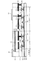
前記受光部は、前記受光画素ごとに分離された複数の下部電極と、光電変換層と、前記受光画素に共通な上部電極とを有し、前記上部電極は、光入射側で取出し端子に接続され、前記取出し端子は前記上部電極と異なる層に形成されていることを特徴とする。
nmの厚さに形成する。
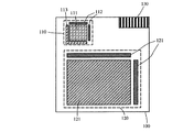
111 受光マトリクス
112 周辺駆動回路
113 端子部
120 画素領域
121 表示マトリクス
122 周辺駆動回路
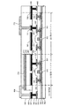
201 活性層
202 選択線
206 信号線
207 ソース電極
208 下部電極
209 n層
210 i層
211 p層
212 上部電極
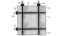
301 活性層
302 選択線
306 信号線
307 ドレイン電極
308 電極層
309 電極
312 画素電極
601、603、606 取出し端子
Claims (1)
- 複数の受光画素を有し、
前記複数の受光画素は、光を電荷に変換する受光部と、前記受光部に電気的に接続されたスイッチング素子とを有し、
前記受光部は、前記複数の受光画素ごとに分離された複数の第1の導電層と、光電変換層と、前記複数の受光画素に共通な第2の導電層とを有し、
前記第2の導電層は、前記第2の導電層の上層に形成された取出し配線と電気的に接続され、
前記取出し配線は、前記第2の導電層の下層に形成された取出し端子と電気的に接続され、
前記取出し配線と前記取出し端子とは、複数のコンタクトホールによって電気的に接続され、
前記複数のコンタクトホールの間隔が、前記複数の受光画素の画素ピッチと等しくなるように配置されていることを特徴とするイメージセンサ。
Priority Applications (1)
| Application Number | Priority Date | Filing Date | Title |
|---|---|---|---|
| JP2008212007A JP5025596B2 (ja) | 2008-08-20 | 2008-08-20 | イメージセンサ |
Applications Claiming Priority (1)
| Application Number | Priority Date | Filing Date | Title |
|---|---|---|---|
| JP2008212007A JP5025596B2 (ja) | 2008-08-20 | 2008-08-20 | イメージセンサ |
Related Parent Applications (1)
| Application Number | Title | Priority Date | Filing Date |
|---|---|---|---|
| JP27345897A Division JP4271268B2 (ja) | 1997-09-20 | 1997-09-20 | イメージセンサおよびイメージセンサ一体型アクティブマトリクス型表示装置 |
Related Child Applications (1)
| Application Number | Title | Priority Date | Filing Date |
|---|---|---|---|
| JP2012062919A Division JP5138107B2 (ja) | 2012-03-20 | 2012-03-20 | イメージセンサ、電子機器 |
Publications (3)
| Publication Number | Publication Date |
|---|---|
| JP2009016855A JP2009016855A (ja) | 2009-01-22 |
| JP2009016855A5 JP2009016855A5 (ja) | 2011-02-03 |
| JP5025596B2 true JP5025596B2 (ja) | 2012-09-12 |
Family
ID=40357294
Family Applications (1)
| Application Number | Title | Priority Date | Filing Date |
|---|---|---|---|
| JP2008212007A Expired - Fee Related JP5025596B2 (ja) | 2008-08-20 | 2008-08-20 | イメージセンサ |
Country Status (1)
| Country | Link |
|---|---|
| JP (1) | JP5025596B2 (ja) |
Cited By (1)
| Publication number | Priority date | Publication date | Assignee | Title |
|---|---|---|---|---|
| JP2950937B2 (ja) | 1990-07-31 | 1999-09-20 | 株式会社マテリアルアンドインテリジェントデバイス研究所 | 電子ビームの偏向格子 |
Families Citing this family (3)
| Publication number | Priority date | Publication date | Assignee | Title |
|---|---|---|---|---|
| KR101610846B1 (ko) | 2009-09-08 | 2016-04-11 | 삼성디스플레이 주식회사 | 표시 장치 및 그 제조 방법 |
| US8975637B2 (en) | 2009-10-07 | 2015-03-10 | Sharp Kabushiki Kaisha | Semiconductor device, process for production of the semiconductor device, and display device equipped with the semiconductor device |
| GB2506631A (en) | 2012-10-04 | 2014-04-09 | Sony Comp Entertainment Europe | Combined image display and sensing device |
Family Cites Families (6)
| Publication number | Priority date | Publication date | Assignee | Title |
|---|---|---|---|---|
| JPS5722251U (ja) * | 1980-07-11 | 1982-02-04 | ||
| JPS6286855A (ja) * | 1985-10-14 | 1987-04-21 | Fuji Photo Film Co Ltd | 放射線用固体撮像素子 |
| JPH02128468A (ja) * | 1988-11-08 | 1990-05-16 | Fujitsu Ltd | 固体撮像装置及びその製造方法 |
| JPH03187267A (ja) * | 1989-12-15 | 1991-08-15 | Mitsubishi Electric Corp | 固体撮像装置 |
| JP3347423B2 (ja) * | 1993-08-31 | 2002-11-20 | キヤノン株式会社 | 液晶表示装置 |
| JPH08186241A (ja) * | 1995-01-06 | 1996-07-16 | Canon Inc | 撮像素子と固体撮像装置 |
-
2008
- 2008-08-20 JP JP2008212007A patent/JP5025596B2/ja not_active Expired - Fee Related
Cited By (1)
| Publication number | Priority date | Publication date | Assignee | Title |
|---|---|---|---|---|
| JP2950937B2 (ja) | 1990-07-31 | 1999-09-20 | 株式会社マテリアルアンドインテリジェントデバイス研究所 | 電子ビームの偏向格子 |
Also Published As
| Publication number | Publication date |
|---|---|
| JP2009016855A (ja) | 2009-01-22 |
Similar Documents
| Publication | Publication Date | Title |
|---|---|---|
| JP4271268B2 (ja) | イメージセンサおよびイメージセンサ一体型アクティブマトリクス型表示装置 | |
| JP4044187B2 (ja) | アクティブマトリクス型表示装置およびその作製方法 | |
| JP4027465B2 (ja) | アクティブマトリクス型表示装置およびその製造方法 | |
| JP5004892B2 (ja) | 半導体装置 | |
| JP4183784B2 (ja) | 液晶パネルの作製方法 | |
| JPH1197664A (ja) | 電子機器およびその作製方法 | |
| JP5025596B2 (ja) | イメージセンサ | |
| JP4700659B2 (ja) | 液晶表示装置 | |
| JP5138107B2 (ja) | イメージセンサ、電子機器 | |
| JP5312442B2 (ja) | 半導体装置、イメージセンサ及び撮影機器 | |
| JP5604579B2 (ja) | 表示装置 | |
| JP4986923B2 (ja) | イメージセンサの作製方法 | |
| JP4163156B2 (ja) | 表示装置 | |
| JP5622812B2 (ja) | 表示装置 | |
| JP4999979B2 (ja) | イメージセンサ及び電子機器 | |
| JP5100799B2 (ja) | 液晶表示装置 |
Legal Events
| Date | Code | Title | Description |
|---|---|---|---|
| A521 | Request for written amendment filed |
Free format text: JAPANESE INTERMEDIATE CODE: A523 Effective date: 20101215 |
|
| A131 | Notification of reasons for refusal |
Free format text: JAPANESE INTERMEDIATE CODE: A131 Effective date: 20120214 |
|
| A521 | Request for written amendment filed |
Free format text: JAPANESE INTERMEDIATE CODE: A523 Effective date: 20120320 |
|
| TRDD | Decision of grant or rejection written | ||
| A01 | Written decision to grant a patent or to grant a registration (utility model) |
Free format text: JAPANESE INTERMEDIATE CODE: A01 Effective date: 20120612 |
|
| A01 | Written decision to grant a patent or to grant a registration (utility model) |
Free format text: JAPANESE INTERMEDIATE CODE: A01 |
|
| A61 | First payment of annual fees (during grant procedure) |
Free format text: JAPANESE INTERMEDIATE CODE: A61 Effective date: 20120619 |
|
| FPAY | Renewal fee payment (event date is renewal date of database) |
Free format text: PAYMENT UNTIL: 20150629 Year of fee payment: 3 |
|
| R150 | Certificate of patent or registration of utility model |
Free format text: JAPANESE INTERMEDIATE CODE: R150 |
|
| FPAY | Renewal fee payment (event date is renewal date of database) |
Free format text: PAYMENT UNTIL: 20150629 Year of fee payment: 3 |
|
| R250 | Receipt of annual fees |
Free format text: JAPANESE INTERMEDIATE CODE: R250 |
|
| R250 | Receipt of annual fees |
Free format text: JAPANESE INTERMEDIATE CODE: R250 |
|
| LAPS | Cancellation because of no payment of annual fees |