JP5025596B2 - Image sensor - Google Patents
Image sensor Download PDFInfo
- Publication number
- JP5025596B2 JP5025596B2 JP2008212007A JP2008212007A JP5025596B2 JP 5025596 B2 JP5025596 B2 JP 5025596B2 JP 2008212007 A JP2008212007 A JP 2008212007A JP 2008212007 A JP2008212007 A JP 2008212007A JP 5025596 B2 JP5025596 B2 JP 5025596B2
- Authority
- JP
- Japan
- Prior art keywords
- light receiving
- film
- matrix
- terminal
- electrode
- Prior art date
- Legal status (The legal status is an assumption and is not a legal conclusion. Google has not performed a legal analysis and makes no representation as to the accuracy of the status listed.)
- Expired - Fee Related
Links
Images


Description
本発明は、光を電荷に変換する受光部と、受光画素を走査して、受光部で発生した電荷を信号として読み出す走査回路を有するイメージセンサに関するものであり、特に走査回路上に受光部を積層した積層型のイメージセンサに関するものである。 The present invention relates to an image sensor having a light receiving unit that converts light into electric charge, and a scanning circuit that scans light receiving pixels and reads out the electric charge generated in the light receiving unit as a signal, and in particular, includes a light receiving unit on the scanning circuit. The present invention relates to a laminated image sensor.
更に、他の発明は積層型のイメージセンサと表示マトリクスとを一体化したアクティブマトリクス型表示装置に関するものである。 Furthermore, another invention relates to an active matrix display device in which a laminated image sensor and a display matrix are integrated.
光センサは、光を電気信号に変換するセンサとして広く用いられている。例えば、ファクシミリ、複写機、ビデオカメラ、デジタルスチルカメラ等のイメージセンサとして広く使用されている。 Optical sensors are widely used as sensors that convert light into electrical signals. For example, it is widely used as an image sensor for facsimile machines, copying machines, video cameras, digital still cameras, and the like.
マルチメディアの要求に対応するため、イメージセンサの画素の高密度化が急激に進んでいる。例えば、デジタルスチルカメラの画素の規格はVGA(640×480=31万画素)から、SVGA、XGAへと高密度化され、更にSXGA(1280×1024=131万画素)へと高密度化が進んでいる。 In order to meet the demand for multimedia, the density of pixels of the image sensor is rapidly increasing. For example, the standard of digital still camera pixels has been increased from VGA (640 × 480 = 310,000 pixels) to SVGA and XGA, and further to SXGA (1280 × 1024 = 1.31 million pixels). It is out.
また、デジタルスチルカメラ等のマルチメディアツールの小型化、低コスト化の要求から、光学系は2/3inchから1/2inch、1/3inch、1/4inchへと年々小型化されている。 In addition, due to the demand for miniaturization and cost reduction of multimedia tools such as digital still cameras, the optical system is miniaturized from 2/3 inch to 1/2 inch, 1/3 inch, and 1/4 inch year by year.
このように、画素の高密度化、光学系の小型化を実現するうえで、小さな受光セルであって、変換効率の良いイメージセンサが要求される。この要求を満足するため、例えば開口率を向上するため、受光部で発生した電荷を信号として読み出す走査回路と、受光部(フォトダイオード部)とを積層した積層型イメージセンサが提案されている。 As described above, an image sensor having a small light receiving cell and a high conversion efficiency is required in order to realize a high density pixel and a small optical system. In order to satisfy this requirement, for example, in order to improve the aperture ratio, a multilayer image sensor in which a scanning circuit that reads out electric charges generated in the light receiving portion as a signal and a light receiving portion (photodiode portion) has been proposed.
近年、ポリシリコンTFTと呼ばれる多結晶シリコンを用いたTFTする技術が鋭意研究されている。その成果として、ポリシリコンTFTによって、シフトレジスタ回路等の駆動回路を作製することが可能になり、表示マトリクスと、表示マトリクスを駆動する周辺駆動回路とを同一基板上に集積したアクティブマトリクス型の液晶パネル実用化に至っている。そのため、液晶パネルが低コスト化、小型化、軽量化されたため、パーソナルコンピュータ、携帯電話、ビデオカメラやデジタルカメラ等の各種情報機器、携帯機器の表示部に用いられている。 In recent years, a technique for performing TFT using polycrystalline silicon called polysilicon TFT has been intensively studied. As a result, it is possible to manufacture a drive circuit such as a shift register circuit by using a polysilicon TFT, and an active matrix type liquid crystal in which a display matrix and a peripheral drive circuit for driving the display matrix are integrated on the same substrate. Panels have been put to practical use. For this reason, liquid crystal panels have been reduced in cost, size, and weight, and are used in various information devices such as personal computers, mobile phones, video cameras and digital cameras, and display units of mobile devices.
現在、ノート型パソコンよりも携帯性に優れ、安価なポケットサイズの小型携帯用情報処理端末装置が実用化されており、その表示部にはアクティブマトリクス型液晶パネルが用いられている。このような情報処理端末装置は表示部からタッチペン方式でデータを入力可能となっているが、紙面上の文字・図画情報や、映像情報を入力するには、スキャナーやデジタルカメラ等の周辺機器が必要である。そのため、情報処理端末装置の携帯性が損なわれてしまっている。また、使用者に周辺機器を購入するための経済的な負担をかけている。 At present, a pocket-sized small portable information processing terminal device that is more portable than a notebook personal computer and is inexpensive has been put into practical use, and an active matrix liquid crystal panel is used for its display section. Such information processing terminal devices can input data from the display unit by a touch pen method, but peripheral devices such as scanners and digital cameras are used to input text / graphics information and video information on paper. is necessary. For this reason, the portability of the information processing terminal device has been impaired. It also puts an economic burden on the user to purchase peripheral equipment.
また、アクティブマトリクス型表示装置は、TV会議システム、TV電話、インターネット用端末等の表示部にも用いられている。これらシステムや、端末では、対話者や使用者の映像を撮影するカメラを備えているが、表示部とカメラ部は個別に製造されてモジュール化されている。 Active matrix display devices are also used in display units of TV conference systems, TV phones, Internet terminals, and the like. These systems and terminals are equipped with a camera that captures images of a conversation person or user, but the display unit and the camera unit are individually manufactured and modularized.
本発明では、積層型のイメージセンサにおいて、さらなる開口率の向上を図ることを課題とし、特に、受光部の光入射側の上部電極を定電位に固定するための取出し端子の構造に関する。 The present invention has an object of further improving the aperture ratio in a multilayer image sensor, and particularly relates to a structure of an extraction terminal for fixing an upper electrode on a light incident side of a light receiving unit to a constant potential.
本発明の目的は、上述した問題点を解消し、表示マトリクス、周辺回路が形成される基板上に、イメージセンサを設けることにより、撮像機能と表示機能とを兼ね備えたインテリジェント化されたアクティブマトリクス型表示装置をすることにある。 An object of the present invention is to provide an intelligent active matrix type that has both an imaging function and a display function by providing an image sensor on a substrate on which a display matrix and peripheral circuits are formed, eliminating the above-described problems. There is a display device.
上述の課題を解決するために本発明は、複数の受光画素が配置された受光画素領域に、光を電荷に変換する受光部と、前記受光部で発生した電荷を信号として読み出す信号読出し部とが積層されたイメージセンサであって、前記受光部は、前記受光画素ごとに分離された複数の下部電極と、光電変換層と、前記受光画素に共通な上部電極とを有し、前記イメージセンサは、前記上部電極と異なる層に形成された取出し端子を有し、前記受光画素領域外部において、前記上部電極は前記取出し端子と光入射側で接続されていることを特徴とする。 In order to solve the above-described problems, the present invention provides a light receiving unit that converts light into electric charge in a light receiving pixel region in which a plurality of light receiving pixels are arranged, and a signal reading unit that reads out the charge generated in the light receiving unit as a signal. Wherein the light receiving unit has a plurality of lower electrodes separated for each light receiving pixel, a photoelectric conversion layer, and an upper electrode common to the light receiving pixels. Has an extraction terminal formed in a different layer from the upper electrode, and the upper electrode is connected to the extraction terminal on the light incident side outside the light receiving pixel region.
更に、本発明は、複数の選択線と複数の信号線が格子状に配置され、複数の画素電極を有する表示マトリクスと、複数の受光画素が配置された受光画素領域に、光を電荷に変換する受光部と、前記受光部で発生した電荷を信号として読み出す信号読出し部とが積層されたイメージセンサとを同一基板上に有するアクティブマトリクス型表示装置であって、
前記受光部は、前記受光画素ごとに分離された複数の下部電極と、光電変換層と、前記受光画素に共通な上部電極とを有し、前記上部電極は、光入射側で取出し端子に接続され、前記取出し端子は前記上部電極と異なる層に形成されていることを特徴とする。
Furthermore, the present invention converts light into electric charges in a display matrix having a plurality of selection lines and a plurality of signal lines arranged in a grid, having a plurality of pixel electrodes, and a light receiving pixel region in which a plurality of light receiving pixels are arranged. An active matrix type display device having an image sensor in which a light receiving unit and a signal reading unit that reads out a charge generated in the light receiving unit as a signal are stacked on the same substrate,
The light receiving unit includes a plurality of lower electrodes separated for each light receiving pixel, a photoelectric conversion layer, and an upper electrode common to the light receiving pixels, and the upper electrode is connected to an extraction terminal on a light incident side. The lead-out terminal is formed in a layer different from the upper electrode.
更に、上記イメージセンサ一体型アクティブマトリクス型表示装置において、前記信号線及び前記選択線を少なくとも覆う電極層を形成し、かつ受光部の下部電極を前記電極層と同じ出発膜で形成することを特徴とする。 Further, in the active matrix display device integrated with an image sensor, an electrode layer covering at least the signal line and the selection line is formed, and a lower electrode of the light receiving portion is formed of the same starting film as the electrode layer. And
更に、イメージセンサ一体型アクティブマトリクス型表示装置において、前記画素マトリクスは、前記基板上に形成され、前記信号線及び前記選択線に接続された能動素子と、前記能動素子を覆う第1の絶縁膜と、前記第1の絶縁膜上に形成され、前記信号線及び前記選択線とを少なくとも覆う電極層と、前記電極層上に形成された第2の絶縁膜と、前記第2の絶縁膜上に形成され、前記能動素子に接続された画素電極とを有し、前記イメージセンサは、前記基板上に形成された前記信号読出し部と、前記信号読出し部を覆う前記第1の絶縁膜と、前記第1の絶縁膜上に形成され前記電極層と同じ出発膜でなり、前記受光画素ごとに分離された複数の下部電極と、前記下部電極上に形成された光電変換層と、前記光電変換層上に形成され、前記受光画素に共通な上部電極と、前記上部電極を覆う前記第2の絶縁膜と、前記第2の絶縁膜上に形成され、前記上部電極に接続された取出し端子とを有し、前記上部電極は、前記画素電極と同じ出発膜で形成されていることを特徴とする。 Furthermore, in the active matrix display device integrated with an image sensor, the pixel matrix is formed on the substrate, and an active element connected to the signal line and the selection line, and a first insulating film covering the active element And an electrode layer formed on the first insulating film and covering at least the signal line and the selection line, a second insulating film formed on the electrode layer, and the second insulating film A pixel electrode connected to the active element, and the image sensor includes the signal readout unit formed on the substrate, the first insulating film covering the signal readout unit, A plurality of lower electrodes formed on the first insulating film and having the same starting film as the electrode layer, separated for each light receiving pixel, a photoelectric conversion layer formed on the lower electrode, and the photoelectric conversion Formed on the layer and before An upper electrode common to a light-receiving pixel; the second insulating film covering the upper electrode; and an extraction terminal formed on the second insulating film and connected to the upper electrode. Is formed of the same starting film as the pixel electrode.
本実施形態では、表示マトリクスと受光マトリクスを同一基板上に形成するために、成膜プロセス及びパターニングプロセスを各マトリクスとで共通化することで、製造コストを安価におさえることができる。 In the present embodiment, since the display matrix and the light receiving matrix are formed on the same substrate, the film formation process and the patterning process are shared by each matrix, so that the manufacturing cost can be reduced.
また本実施形態では、受光部の上部電極の電位を固定するための取出し端子を上部電極と一体的に形成しないことにより、受光部の上部電極と光電変換層とのパターニングを連続して行うことが可能になり、マスクずれによる開口率の低下を防止できる。さらにこの取出し端子を表示マトリクスの画素電極と同一出発膜で形成することにより、プロセスの簡略化が図れる。 In the present embodiment, the extraction electrode for fixing the potential of the upper electrode of the light receiving unit is not formed integrally with the upper electrode, so that the upper electrode of the light receiving unit and the photoelectric conversion layer are continuously patterned. It is possible to prevent the aperture ratio from being lowered due to mask displacement. Furthermore, the process can be simplified by forming the extraction terminal with the same starting film as the pixel electrode of the display matrix.
図1を用いて、本実施形態の周辺回路一体型のアクティブマトリクス型表示装置において、素子基板にイメージセンサを一体的に設けた表示装置を説明する。 A display device in which an image sensor is integrated with an element substrate in the peripheral circuit integrated active matrix display device of this embodiment will be described with reference to FIG.
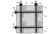
基板500上には、受光マトリクス111と表示マトリクス121が形成されている。表示マトリクス121には、信号線307及び選択線302が格子状に配列され、この格子内に、信号線307及び選択線302接続されたTFTでなる能動素子が表示画素ごとに配置されている。
A
表示マトリクス121には、TFTを覆う第2の絶縁膜540と、第2の絶縁膜540上に形成され、選択線302及び信号線307とを少なくとも覆う電極層308が配置されている。図1において、電極層308は分断されているように図示されているが、格子状に一体的に配置されている。
In the
電極層308上には第3の絶縁膜550が形成され、第3の絶縁膜550上には画素電極312が形成されている。画素電極312は第1、第2の絶縁膜540、550に設けられたコンタクトホールを介して表示マトリクスのTFTに接続されている。
A third
電極層308は、表示マトリクス121に配置されている能動素子に光が入射するのを防止すると共に、有効表示領域からの光が表示に寄与して、表示特性が劣化するのを防いでいる。また電極層308の電位を固定することにより、選択線302、信号線306の電位の変動が、画素電極312の電位にフィードバックされることが防止できる。
The
他方、受光マトリクス111には、信号読取り部として、TFTをスイッチング素子として用い受光画素を走査するための走査回路が配置されている。信号読取り部は、表示部の能動素子と同様、第1の絶縁膜540に覆われている。第1の絶縁層540上には、受光部が形成されている。第2の絶縁ゲイト型半導体素子により、受光部で発生した電荷、もしくは受光部の電位の変化が信号として読み出される。
On the other hand, the
受光部は、受光画素ごとに分離された複数の下部電極208と、下部電極208上に形成された光電変換層210と、光電変換層210上に形成され、受光画素に共通な上部電極212とで構成されている。下部電極212は電極層308と同じ出発膜で形成されている。受光部は第2の絶縁膜550によってパッシベーションされている。
The light receiving unit includes a plurality of
光電変換膜210は真性もしくは実質的に真性な非晶質シリコンや非晶質シリコンゲルマニューム等のシリコン系半導体を用いることができる。pin接合を有するシリコン系半導体膜を用いることもできる。また受光部をフォトコンダクタとする場合には、一般に固体撮像管に用いられてるZnSe/ZnCdTe膜や、Se/Te/As等の積層膜を用いることができる。
For the
なお、図1において、膜209、膜211は非晶質シリコンでなる光電変換層210を下部電極208、上部電極212にオーミック接合させるためのn型、p型非晶質シリコン膜である。なお、n型非晶質シリコン膜209の代わりに、非晶質シリコン膜210のバリア膜として機能する膜を設けても良い。この場合、リン等のn型不純物が添加された酸化珪素膜、窒化珪素膜、炭化珪素膜等を用いることができる。
In FIG. 1, a
上部電極212の電位を固定するために、前記受光マトリクス111外部において、受光部の上部電極212は、第3の絶縁膜550に設けられたコンタクトホールを介して、画素電極312と同じ出発膜でなる取出し配線606に接続されている。
In order to fix the potential of the
更に、取出し配線606は、電極層308と同じ出発膜でなる取出し端子603に接続され、さらに取出し端子603は信号線307と同じ出発膜でなる取出し端子601に接続されている。取出し端子601は基板外部の配線との接続部となる外部端子に、直接もしくは他の配線を介して接続されている。取出し端子601を一定電位に固定することにより、上部電極212の電位が一定に固定できる。
Further, the
積層型イメージセンサにおいて、開口部が全て上部電極212に覆われ、その電位が一定に固定されるため、光入射側から侵入する雑音を上部電極212にてシールドすることができる。さらに、本実施形態では、受光部の側面は、端子601、603、606で囲まれ、これら端子の電位は一定に固定されるため、受光部側面からの雑音が侵入することも抑制できる。よって、S/N比が向上でき、高性能、高信頼性のイメージセンサを提供できる
In the multilayer image sensor, since all the openings are covered with the
本実施形態では、表示マトリクス121と受光マトリクス111を同一基板上に形成するために、成膜プロセス及びパターニングプロセスを各マトリクス111、121とで共通化することを特徴とする。絶縁膜540、550を各マトリクス111、121で共有する。
In this embodiment, in order to form the
更に電極層308と下部電極208、画素電極312と取出し端子606とを同一の成膜プロセス及びパターニングプロセスで形成する。これにより、追加工程を最小限にして、イメージセンサ一体型のアクティブマトリクス型表示装置を提供することが可能であり、製造コストを安価におさえることができる。
Further, the
また本実施形態では、受光部の上部電極212の電位を固定するために、上部電極212を外部端子に接続するための取出し端子606を、上部電極212と一体的に形成しづらい点に特徴を有する。この取出し端子606を上部電極212と異なる層に形成し、かつ上部電極212の光入射側で接続することにある。
Further, the present embodiment is characterized in that it is difficult to integrally form an
この取出し端子606を上部電極212と一体的に形成した場合には、上部電極212と光電変換層210とのパターンが異り、上部電極212のパターニング工程は光電変換層210と異なることとなる。このため、上部電極212のパターニングのマスクずれにより、開口率が低下するおそれがある。
When the
他方、上部電極212と取出し端子とをそれぞれ異なる層に配置された導電膜で構成することにより、1つのレジストマスクを用いて、上部電極212と光電変換層210とのパターニングを連続して行うことが可能になり、マスクずれによる開口率の低下を防止するという効果を得る。更に光電変換層210をパターニングする際に、光電変換層210上には上部電極212が存在するため、光電変換層210のパターニングプロセス時のダメージを抑制することができる。
On the other hand, by patterning the
本実施形態では、上部電極212と取出し端子606とをそれぞれ異なる層に配置された導電膜で構成する。上部電極212と光電変換層210とを同じプロセスでパターニングするには、この導電膜は上部電極212よりも上部に形成することも重要であり、取出し端子606を上部電極212の光入射側で接続させる。またこの取出し端子606を画素電極312と同じプロセスによって形成することにより、アクティブ型表示装置の製造プロセスとの整合性をとる。
In the present embodiment, the
図1〜図16を用いて、本発明の実施例を詳細に説明する。 The embodiment of the present invention will be described in detail with reference to FIGS.
本実施例は、イメージセンサと表示マトリクスとを同一基板上に備えた透過型液晶表示装置に関するものである。 This embodiment relates to a transmissive liquid crystal display device provided with an image sensor and a display matrix on the same substrate.
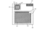
図2は、本実施例の液晶表示装置の正面図である。図2に示すように基板100上には、受光領域110と表示領域120とが共に設けられている。受光領域110には、複数の受光画素がマトリクス状に配置された受光マトリクス111と、受光マトリクス111に接続された周辺回路112と、周辺回路が接続されていない受光マトリクス111の周囲を囲むように、取出し端子が配置される端子部113とが形成されている。受光マトリクス111は、受光部(フォトダイオード)と、受光部で発生した電荷を信号として読み出すための半導体素子が積層した構造を有する。
FIG. 2 is a front view of the liquid crystal display device of this embodiment. As shown in FIG. 2, a
他方、表示領域120は、画素電極と画素電極に接続された能動素子とが配置された表示マトリクス121と、表示マトリクス121配置された能動素子を駆動するための周辺駆動回路122とが設けられている。更に、基板100上には、基板外部の電源線等の配線との接続部となる外部取出し端子部130が設けられている。
On the other hand, the
本実施例では、受光マトリクス111の絶縁ゲイト型半導体素子、表示マトリクス121の能動素子、及び周辺駆動回路112、122に配置される半導体素子を、CMOS技術を用いてTFT(薄膜トランジスタ)にて同時に作製する。以下に本実施例の液晶パネルの作製方法を説明する。
In this embodiment, the insulating gate type semiconductor element of the
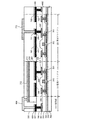
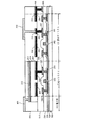
図3、図4には、受光マトリクス111、取出し端子部113及び表示マトリクス121の断面図を示す。また、図5〜図8には受光領域121の作製過程を示す正面図を示し、図9〜図12には表示マトリクス121の作製過程を示す正面図を示し、図13、図14には周辺回路112、122に配置されるCMOS−TFTの作製過程を示す正面図を示す。
3 and 4 are cross-sectional views of the
まず図3(A)に示すように、ガラス基板500全面に、基板からの不純物の拡散を防止するための下地膜510を形成する。下地膜510として、プラズマCVD法によって、酸化珪素膜を200nmの厚さに形成する。
First, as shown in FIG. 3A, a
図3(A)の受光マトリクス111、表示マトリクス121及びCMOS−TFTの正面図が図5、図9、図13に相当する。図5、図9において線A−A’、線B−B’に沿った断面図が図3(A)に対応する。
Front views of the
本実施例では透過型液晶パネルを作製するため、基板500は可視光を透過する基板であれば良く、ガラス基板500の代わりに石英基板等も用いることができる。なお、本実施例では、TFTを多結晶シリコン膜で形成するため、基板500は多結晶シリコン膜の形成プロセスに耐え得るものを選択する。多結晶シリコン膜は移動度が10〜200cm2 /Vsec程度と非常に大きく、多結晶シリコンでTFTのチャネル形成領域を構成することにより、高速応答させることができ、特に、受光マトリクス110のTFTや、周辺駆動回路112、122のCMOS−TFTに有効である。
In this embodiment, since a transmissive liquid crystal panel is manufactured, the
次に、プラズマCVD法によって非晶質シリコン膜を55nmの厚さに成膜し、エキシマレーザ光を照射して、多結晶化する。非晶質珪素膜の結晶化方法として、SPCと呼ばれる熱結晶化法、赤外線を照射するRTA法、熱結晶化とレーザアニールとを併用する方法等を用いることができる。 Next, an amorphous silicon film having a thickness of 55 nm is formed by plasma CVD and irradiated with excimer laser light to be polycrystallized. As a method for crystallizing the amorphous silicon film, a thermal crystallization method called SPC, an RTA method of irradiating infrared rays, a method using thermal crystallization and laser annealing in combination, or the like can be used.
次に、多結晶化されたシリコン膜を島状にパターニングして、TFTの活性層201、301、401、402を形成する。次に、これら活性層201、301、401、402を覆うゲイト絶縁膜520を形成する。ゲイト絶縁膜520はシラン(SiH4)とN2Oを原料ガスに用いて、プラズマCVD法で120
nmの厚さに形成する。
Next, the polycrystallized silicon film is patterned into an island shape to form
It is formed to a thickness of nm.
次に、Al、Cr、Mo等の金属や導電性ポリシリコン膜等の導電膜を成膜しパターニングして、選択線202、302、ゲイト電極403を形成する。これら配線・電極202、302、403をマスクにして、公知のCMOS技術を用いて活性層201、301、401、402に導電性を付与する不純物をドーピングしてソース及びドレイン領域を形成する。
Next, a conductive film such as a metal such as Al, Cr, or Mo or a conductive polysilicon film is formed and patterned to form
活性層201にリンをドープすることにより、N型のソース領域203、ドレイン領域204、チャネル形成領域205が自己整合的に形成され、活性層301にリンをドープすることにより、N型のソース領域303、ドレイン領域304、チャネル形成領域305が自己整合的に形成され、活性層401にリンをドープすることにより、N型のソース領域、ドレイン領域、チャネル形成領域が自己整合的に形成される。活性層201、301、401をレジストマスクで覆い、活性層402のみにボロンをドープして、P型のソース領域およびドレイン領域と、チャネル形成領域を自己整合的に形成する。ドーピング後、ドーピングされた不純物を活性化する。
By doping the
なお、本実施例では活性層201、301、401が多結晶シリコンであるため、配線・電極202、302、403を形成する前に、少なくともNチャネル型TFTのチャネル形成領域となる領域にボロン等のP型の不純物を添加して、しきい値を最適化するのが好ましい。
In this embodiment, since the
次に、図3(B)に示すように、基板500全面を覆う第1の層間絶縁膜530を形成する。層間絶縁膜530に各TFTのソース領域およびドレイン領域に達するコンタクトホール及びCMOS−TFTのゲイト電極403に達するコンタクトホールをそれぞれ形成する。しかる後、チタン膜、アルミニウム膜、チタン膜でなる積層膜を形成し、パターニングして、受光マトリクス111の信号線206、ソース電極207と、表示マトリクス121の信号線306、ドレイン電極307がそれぞれ形成される。
Next, as shown in FIG. 3B, a first
この状態の受光マトリクス111、表示マトリクス121の正面図が図6、図10に相当する。図6、図10において線A−A’、線B−B’に沿った断面図が図3(A)に対応する。
Front views of the
更にCMOS−TFTには、図14に示すようにゲイト電極403に接続される入力配線411、nチャネル型TFTのソース領域に接続される配線412、pチャネル型TFTのドレイン領域に接続される配線413、Nチャネル型TFTのドレイン領域406とPチャネル型TFTのソース領域408とを接続する配線414を形成する。
Further, as shown in FIG. 14, the CMOS-TFT includes an
図6に示すように、受光マトリクス111において、選択線202は周辺回路122Hに接続され、周辺回路122Hから、受光部で発生した信号電荷を読み取る受光画素を指定する選択信号が入力される。また信号線206は周辺回路112Vに接続され、読み出された信号電荷は、信号線206を経て周辺回路112Vに出力され、周辺回路112Vから映像信号として外部に出力される。
As shown in FIG. 6, in the
さらに、取出し端子部113には、取出し端子601が形成される。図6に示すように、取出し端子601は、受光マトリクス111の周囲であって周辺駆動回路112が接続されていない周囲に沿って『L』字型に形成されている。更に取出し端子601は受光領域110外部に延在する部分を有し、この部分で外部取出し端子部130に形成された端子に接続されている。
Furthermore, an
更に、表示領域120内において、表示マトリクス121外部に後に形成される電極層308の電位を固定するための端子602も形成される。
Further, a terminal 602 for fixing the potential of an
以上のCMOSプロセスを経て、多結晶シリコンTFTを用いた受光マトリクス111、表示マトリクス121及び駆動回路112、122に配置されるCMOS−TFTが同時に完成する。ここでは、これらTFTをトップゲイトのプラナ型としたが、逆スタガ等のボトムゲイト型としてもよい。この場合、活性層201、301、401、402と選択線202、302、ゲイト電極403の形成順序を逆にし、選択線202、302、ゲイト電極403を形成した後、ゲイト絶縁膜520を形成すればよい。また、LDD領域やオフセット領域を設けてもよい。
Through the CMOS process described above, CMOS-TFTs disposed in the
次に、図3(C)に示すように、受光部TFT200と受光部とを絶縁分離するための第2の層間絶縁膜540を基板500全面に形成する。第2の層間絶縁膜540には下層の凹凸を相殺して、平坦な表面が得られる樹脂膜が好適である。このような樹脂膜として、ポリイミド、ポリアミド、ポリイミドアミド、アクリルを用いることができる。また、第2の層間絶縁膜540の表面層は平坦な表面を得るため樹脂膜とし、下層は酸化珪素、窒化珪素、酸化窒化珪素等の無機絶縁材料の単層、多層としても良い。本実施例では、第2の層間絶縁膜540としてポリイミド膜を1.5μmの厚さに形成する。
Next, as shown in FIG. 3C, a second
次に、第2の層間絶縁膜540に、ソース電極207、ドレイン電極307、端子601、602に達するコンタクトホールをそれぞれ形成した後、受光部の下部電極、及び表示マトリクスの電極層を構成するTi、Cr、Mo、Al等の導電膜11を形成する。本実施例では導電膜として厚さ200nmのチタン膜11をスッパタ法で成膜する。
Next, contact holes reaching the
次に、受光部の光電変換層と下部電極とをオーミック接合させるためのn型の非晶質シリコン膜12を30〜50nmの厚さに、ここでは30nmの厚さに基板全面に成膜する。チタン膜11及びシリコン膜12をパターニングするためのレジストマスク13を形成する。
Next, an n-type
レジストマスク13を用いて、図4(A)に示すようにシリコン膜12、チタン膜11を順次パターニングする。ここでは、ドライエッチング法を用いる。シリコン膜12のエッチングガスにはCF4を1〜10%混合したO2ガスを用いる。本実施例ではCF4の濃度を5%とする。またチタン膜11のエッチングガスにはCl2 /BCl3/SiCl4を混合した塩素系ガスを用いる。なお、チタン膜11は樹脂でなる絶縁膜540上に形成されるため、チタン膜11のエッチングガス、エッチャントは樹脂を変質しないものを選択する必要がある。
Using the resist
チタン膜11をパターニングすることにより、図4(A)に示すように、受光マトリクス111には、受光部の下部電極208、表示マトリクス121の電極層308、画素電極との接続用電極309、および端子部113の端子603が形成される。これらチタンでなる電極208、308、309、603上には、チタン膜11と概略同一形状にパターニングされたシリコン膜11でなるn層209、310、311、604が形成される。
By patterning the
受光マトリクス以外のn層310、311、604は実質的な機能を有しないため、形成しなくともよい。この場合はチタン膜11とシリコン膜12のパターニングを別々に行えばよい。しかし、チタン膜11とシリコン膜12のパターニングを同時に行うことで、工程が簡略化できる。
The n layers 310, 311, and 604 other than the light receiving matrix do not have a substantial function and thus may not be formed. In this case, the
なお、受光部のn層209として非晶質シリコンの代わりに微結晶シリコンを用いることもできる。また、リン等のn型不純物が添加された窒化珪素、酸化珪素、炭化珪素を用いることができる。
Note that microcrystalline silicon can be used instead of amorphous silicon for the
この状態の受光領域110および表示マトリクス120の上面図を図7(A)、図11にそれぞれ示す。なお、図7、図11において、n層209、310、311、604は省略されている。
7A and 11 are top views of the
図7(A)に示すように、下部電極208は選択線202、信号線206で形成された格子内に、受光画素ごとに分離されて形成されている。また端子部113には、取出し端子601と接続される端子603が形成されている。端子603は端子601と同様に、周辺駆動回路112と接続されていない受光マトリクス111の周囲に沿って、『L』字型に形成されている。図7(A)の線A−A’による断面図が図4(A)に図示されている。
As shown in FIG. 7A, the
図7(B)に示すように、端子601と端子603とは絶縁膜540に形成された複数のコンタクトホールを介して上下間で接続されている。コンタクトが小さいほどアンテナ効果が緩和されるため、端子601と603は複数のコンタクトホール605により接続する。なお。図7(A)の線D−D’による断面図が図7(B)に相当する。コンタクトホール605のピッチは例えば受光画素のピッチと同程度であれば、上部電極を等電位にするのに問題がない。
As shown in FIG. 7B, the terminal 601 and the terminal 603 are connected to each other through a plurality of contact holes formed in the insulating
他方、表示マトリクス121には、図11に示すように電極層308が、選択線302、信号線306および、電極307とのコンタクト部を除いた活性層301を覆うように格子状に一体的に形成されている。電極層308は受光部に光が入射するのを防ぐと共に、有効表示領域以外から光が漏れることを防止している。さらに、電極層308は表示マトリクス121外部において、取出し配線602に接続されている。取出し配線602はその電位が一定電位に固定されるため、電極層308の電位も一定電位に固定される。これにより、電極層308の下層の選択線302、信号線306の電位の変動によって、電極層308の上層の画素電極の電位が変動することを抑制できる。
On the other hand, in the
次に、チタン膜11、シリコン膜のパターニング終了後、図4(A)に示すように、真性もしくは実質的に真性な非晶質シリコン膜14を1〜2μm、ここでは1.5μmの膜厚に形成し、連続してボロンを含んだp型の非晶質シリコン膜15を30〜100nmの厚さに、ここでは50nmの厚さに成膜する。さらに、受光部の上部電極を構成する透明導電膜、ここではITO膜16を120nmの厚さに成膜する。そして、これら膜14〜16をパターニングするためのレジストマスク17を形成する。
Next, after the patterning of the
なお、非晶質シリコン膜14が実質的に真性な状態とは、ボロン等のp型不純物を5×10¹⁶〜1×1019cm-3程度添加し、そのフェルミ準位がバンドギャプの中央に位置した状態をいう。これは非晶質シリコンは成膜時にはフェルミ準位がバンドギャプの中央に必ずしも位置している訳ではなく、若干n型になる方向にフェルミ準位がずれている。そのため、上記のようにp型不純物を添加することで、フェルミ準位をバンドギャプの中央にすることができる。この場合に不純物が添加されているが、フェルミ準位をバンドギャプの中央にある状態を実質的に真性な状態であるとしている。
The substantially intrinsic state of the
なお、真性または実質的に真正な非晶質シリコン膜14の代わりに非晶質シリコンゲルマニュームを用いることができる。また、p型非晶質シリコン膜15の代わりに微結晶シリコンを用いることもできる。
An amorphous silicon germanium can be used instead of the intrinsic or substantially intrinsic
次に、レジストマスク17を用いて、ITO膜16、シリコン膜15、14を順次パターニングして、図4(B)に示すように、上部電極212、p層211、i層210をそれぞれ形成する。ITO膜16、シリコン膜15、14をパターニングするには、CF4/SF6/O2を混合したエッチングガスを用いたRIEエッチングを用いる。なお、ITO膜16をパターニングした後は、シリコン膜のみをエッチングするガスを用いることにより、上部電極212をマスクにしてシリコン膜15、14をエッチング可能であるため、レジストマスク17は不要になる。しかしシリコン膜15、14のエッチング時に、レジストマスク17を残存させることで、RIEエッチングによって上部電極212が変質することを防止できる。
Next, the
本実施例では、シリコン膜15、14とITO膜16とのパターニング工程を連続して行う、即ち、ITO膜成膜前にシリコン膜15、14の成膜の間にパターニング工程を行わないことで、上部電極212と光電変換層210とのパターンずれによる開口率低下を回避することができる。
In this embodiment, the patterning process of the
また上部電極212とp層211、i層210を、受光マトリクス111内のみでなく、端子部113側に突出させて形成する。これは、後に、開口率を低下することなく、上部電極212を電極604に接続させるためであり、製造マージンや受光部の信頼性を考慮して、端子部113側に突出させる幅は、受光画素のピッチの2〜10倍程度とすればよい。
Further, the
また、受光部の信頼性の点から、i層210において、受光マトリクス111の境界部を絶縁化して、受光マトリクス111外部のi層210で発生したフォトキャリアが受光マトリクス111内に漏れ込むことを防止すると良い。絶縁化の方法の1つとして、受光マトリクス111の境界部に沿ってi層210に溝部を形成し、この溝部に絶縁物を埋め込む方法が挙げられる。この溝部はi層210を完全に分断するように形成しても良い。なお、上記のように境界部を絶縁化する場合は、シリコン膜14、15のパターニング工程と、ITO膜16のパターニング工程を別々に行う必要がある。
In addition, from the point of reliability of the light receiving unit, the boundary portion of the
次にレジストマスク17を除去した後、図1に示すように、表示マトリクス121の画素電極312の下地となる第3の層間絶縁膜550を基板500全面に形成する。絶縁膜550受光マトリクス111のパッシベーション膜としても機能する。第3の層間絶縁膜550を構成する絶縁被膜として、ポリイミド、ポリアミド、ポリイミドアミド、アクリル等の樹脂膜を形成して、平坦な表面を得るようにする。本実施例では、ポリイミド膜を形成し、受光マトリクス111での膜厚が、0.3〜1μm、ここでは0.5μmとなる成膜にする。
Next, after removing the resist mask 17, as shown in FIG. 1, a third
次に層間絶縁膜550に、上部電極212、電極309および端子603に達するコンタクトホールを形成する。ここでは、エッチングガスにはCF4を1〜10%混合したO2ガスを用いたRIEエッチング法を用いる。層間絶縁膜550は樹脂でなるためO2ガスのみでエッチング可能であるが、CF4混合することにより、電極309、604上のシリコン膜でなるn層310、604もエッチングされる。
Next, contact holes reaching the
コンタクトホールを開口後、100〜300nm厚さ、ここでは120nmのITO膜をスパッタ法にて成膜し、CF4/SF6/O2を混合したエッチングガスを用いてパターニングして、電極309に接続された画素電極312、および上部電極212を端子603に接続するための取出し端子606が形成される。この状態の受光マトリクス111、表示マトリクス121の上面図をそれぞれ、図8(A)、図12に示す。
After opening the contact hole, an ITO film having a thickness of 100 to 300 nm, here 120 nm, is formed by sputtering, and patterned by using an etching gas mixed with CF 4 / SF 6 / O 2.
図8(A)に示すように、取出し端子606は端子603同様、受光マトリクス111の駆動回路121が接続されていない周囲を囲むように、『L』字型に形成されている。そして、端子606は受光マトリクス111外部において上部電極212に接続され、端子部113において端子603に接続されている。この構造により、取出し端子601を一定電位に固定することにより、上部電極212は端子606、603を介して、その電位が一定電位に固定される。例えば、端子601を一定電位に固定するには、端子601を図1に示す取出し端子部130に形成される外部取出し端子に接続する。この場合、外部取出し端子を信号線206、306と同一の導電膜で形成して、外部取出し端子と取出し端子601を一体的に形成することも可能である。
As shown in FIG. 8A, like the terminal 603, the
なお、上部電極212の全体を一定電位にするためには、端子606を接続するためのコンタクトホール607は受光画素のピッチと同程度とすればよい。なお、図8(A)の線D−D’による断面図を図8(B)に示す。また図8(A)の線A−A’による断面図が図1に図示されている。
In order to make the entire
ここで、端子601、603、606は受光マトリクス111が駆動回路121と接続されていない周囲を囲むように形成したため、図1の断面構成からも明らかなように、受光部(フォトダイオード)側面が端子601、端子603、606で囲まれている。ここでは、端子601、端子603、606は電位が一定に固定されているため、受光部に対するシールドとして機能させることができる。よって、表示マトリクス121と受光マトリクス111を同一基板に設けても、受光部の信頼性を保つことができる。
Here, since the
さらに、選択線202、信号線302が周辺回路112H、112Vとの接続端の他端も端子601、603、606によって、電気的に保護できるため、受光マトリクス111に配置されるTFTの静電破壊を抑制できる。
Further, since the other end of the connection end of the
他方、表示マトリクス121においては、図12に示すように、画素電極312は表示画素ごとに電気的に分離され、その周縁が電極層308と重なるように形成される。この構造により、絶縁膜550を誘電体とし、電極層308、画素電極312を対向電極とする補助容量が形成できる。なお、図12において電極層308上のn層309は省略されている。
On the other hand, in the
実施例において、受光マトリクス111をTFTを作製した後、TFT上に受光部(フォトダイオード)を形成する積層型としたので、従来のように受光部を非晶質シリコン膜で形成しても、受光TFT200を多結晶シリコンで構成することができる。よって、ガラス基板等の絶縁性基板上に、変換効率が良く、高速応答可能なイメージセンサが作製できる。
In the embodiment, since the
また、イメージセンサを積層構造とすることで、従来多結晶シリコンTFTで構成されている液晶パネルの作製工程と整合性が保たれる。従って、イメージセンサと液晶パネルの各特性を損なうことなく同一基板上に集積化できる。 In addition, since the image sensor has a stacked structure, consistency with a manufacturing process of a liquid crystal panel conventionally configured with a polycrystalline silicon TFT is maintained. Therefore, the image sensor and the liquid crystal panel can be integrated on the same substrate without deteriorating the characteristics.
本実施例では、受光マトリクス111に受光画素を2次元に配列したが、受光画素を1次元に配列したラインセンサとしても良い。また、受光画素のフォーマットを表示部のフォーマットと同一にすると、受光画素と表示画素が1対1に対応するため、受光マトリクス111で検出された画像を表示マトリクス121に表示するための信号処理が簡単化、高速化できる。ラインセンサとした場合も、受光画素数は、列方向又は行方向の表示画素数と同じにすると良い。
In this embodiment, the light receiving pixels are two-dimensionally arranged in the
画素フォーマットを一致させた場合には、例えば表示マトリクス121のフォーマットを640×480(VGA規格)とし場合には、1つの受光画素ピッチを10μm程度とすると、受光マトリクス111の占有面積は6.4mm×4.8mm程度となり、液晶パネルに集積化することは可能である。
When the pixel formats are matched, for example, when the format of the
本実施例では、受光部を抵抗型のフォトダイオードとしたため、下部電極208、上部電極とオーミック接合させるn層209、p層211を設けたが、例えばショットキー型とする場合は、n層209、p層211を省略すればよい。
In this embodiment, since the light receiving portion is a resistance type photodiode, the
本実施例では、透過型液晶パネルとしたが、画素電極312を鏡面表面を有する反射型電極とし、直視型の液晶パネルとすることもできる。
In this embodiment, the transmission type liquid crystal panel is used. However, the
本実施例では、受光マトリクス111において、受光部(フォトダイオード)と接続される信号読出し回路として、スイッチング素子として機能するTFTを1つ設けたパッシブ型としたが、例えば、増幅機能を有するアクティブ型とし、複数のTFTで構成することもできる。
In this embodiment, in the
本実施例は、受光領域111の端子部113の変形例である。本実施例を図15を用いて説明する。
The present embodiment is a modification of the
本実施例では、信号線306と同じ出発膜でなる端子601を省略する。この場合、最下層の配線701は電極層308と同一の出発膜でなる配線となる。配線701の形状は、実施例1の端子601と同様とし、受光マトリクス111外部へ延長して、外部取出し端子部130に形成される端子と接続するようにすればよい。
In this embodiment, the terminal 601 made of the same starting film as the
本実施例は、受光領域111の端子部113の変形例である。本実施例を図16を用いて説明する。
The present embodiment is a modification of the
本実施例では、端子601及び電極308を省略する。この場合、端子部113に配置される配線801は画素電極312と同一の出発膜でなる配線のみとなる。配線801の形状は、実施例1の端子601と同様とし、受光マトリクス111外部に延在して、外部取出し端子部130に形成される端子と接続するようにすればよい。
In this embodiment, the terminal 601 and the
本実施例は、受光領域111の端子部113の変形例である。実施例1では端子部の最下層の端子601と信号線306と同じ出発膜で形成したが、選択線302と同じ出発膜で構成することも可能である。
The present embodiment is a modification of the
本実施例の受光領域111の端子部113の変形例である。実施例1において電極層308と同じ出発膜でなる端子603を省略して、端子606と端子601を直接に接続する。また、この場合、実施例4で述べたように、端子601を選択線302と同じ出発膜で構成することも可能である。
It is a modification of the
本実施例は、実施例1で説明した、イメージセンサ一体型の液晶パネルの応用製品を説明する。図17に本実施例の電子機器の模式的な外観図を示す。 In this embodiment, an application product of the image sensor integrated liquid crystal panel described in the first embodiment will be described. FIG. 17 shows a schematic external view of the electronic apparatus of this embodiment.
実施例1の液晶パネルは撮像機能を有する受光領域と、表示領域が一体的に設けられているため、TV会議システム、TV電話、インターネット用端末やパーソナルコンビュータ等の通信機能を備えた表示部に好適である。例えば、表示部で対話者の端末から送信された映像を見ながら、受光マトリクスで自身の姿を撮影して、対話者の端末にその映像を転送することできるので、動画像を双方向通信することが可能である。 Since the liquid crystal panel of the first embodiment is provided with a light receiving area having an imaging function and a display area, the display panel having a communication function such as a TV conference system, a TV phone, an Internet terminal, or a personal computer is provided. Is preferred. For example, while watching the video transmitted from the conversation person's terminal on the display unit, you can take a picture of yourself with the light-receiving matrix and transfer the picture to the conversation person's terminal, so you can communicate the moving image bidirectionally It is possible.
またこのような電子機器の1つとして、図17(A)に、液晶パネルを有するノート型パソコン2000を示す。2001が液晶パネルであり、2002がイメージセンサ部である。
As one of such electronic devices, FIG. 17A illustrates a notebook
また他の電子機器として、図17(B)に、テレビ電話2010を示す。2011が液晶パネルであり、2012がイメージセンサ部である。使用者は自身の姿を姿をイメージセンサ部2012で撮影しつつ、また液晶パネルにて2011通話相手の姿を見ながら通話することができる。
As another electronic device, a
更に図17(C)にはペン入力型の携帯型情報端末機器2020を示す。2021が液晶パネルであり、2021がエリアセンサ部である。エリアセンサ2021により、名紙等の文字・図画情報を取り込んで、液晶パネル2021に表示したり、携帯型情報端末機器内にこれらの情報を保存できるようになっている。
Further, FIG. 17C shows a pen input type portable
本発明では液晶パネルとセンサ部を同一基板に設けたため、小型、軽量でとすることができる。またセンサ部の駆動を液晶パネルと共有化することも可能であるため、省電力化が図れる。よって、図17で示したような、バッテリー駆動型の電子機器に本発明は好適である。 In the present invention, since the liquid crystal panel and the sensor portion are provided on the same substrate, the size and weight can be reduced. Further, it is possible to share the drive of the sensor unit with the liquid crystal panel, so that power saving can be achieved. Therefore, the present invention is suitable for battery-driven electronic devices as shown in FIG.
110 受光領域
111 受光マトリクス
112 周辺駆動回路
113 端子部
120 画素領域
121 表示マトリクス
122 周辺駆動回路
201 活性層
202 選択線
206 信号線
207 ソース電極
208 下部電極
209 n層
210 i層
211 p層
212 上部電極
301 活性層
302 選択線
306 信号線
307 ドレイン電極
308 電極層
309 電極
312 画素電極
601、603、606 取出し端子
110
Claims (1)
前記複数の受光画素は、光を電荷に変換する受光部と、前記受光部に電気的に接続されたスイッチング素子とを有し、
前記受光部は、前記複数の受光画素ごとに分離された複数の第1の導電層と、光電変換層と、前記複数の受光画素に共通な第2の導電層とを有し、
前記第2の導電層は、前記第2の導電層の上層に形成された取出し配線と電気的に接続され、
前記取出し配線は、前記第2の導電層の下層に形成された取出し端子と電気的に接続され、
前記取出し配線と前記取出し端子とは、複数のコンタクトホールによって電気的に接続され、
前記複数のコンタクトホールの間隔が、前記複数の受光画素の画素ピッチと等しくなるように配置されていることを特徴とするイメージセンサ。 Having a plurality of light receiving pixels,
The plurality of light receiving pixels include a light receiving unit that converts light into electric charge, and a switching element that is electrically connected to the light receiving unit,
The light receiving unit includes a plurality of first conductive layers separated for each of the plurality of light receiving pixels, a photoelectric conversion layer, and a second conductive layer common to the plurality of light receiving pixels,
The second conductive layer is electrically connected to an extraction wiring formed in an upper layer of the second conductive layer;
The extraction wiring is electrically connected to an extraction terminal formed in a lower layer of the second conductive layer ,
The extraction wiring and the extraction terminal are electrically connected by a plurality of contact holes,
An image sensor , wherein an interval between the plurality of contact holes is arranged to be equal to a pixel pitch of the plurality of light receiving pixels .
Priority Applications (1)
| Application Number | Priority Date | Filing Date | Title |
|---|---|---|---|
| JP2008212007A JP5025596B2 (en) | 2008-08-20 | 2008-08-20 | Image sensor |
Applications Claiming Priority (1)
| Application Number | Priority Date | Filing Date | Title |
|---|---|---|---|
| JP2008212007A JP5025596B2 (en) | 2008-08-20 | 2008-08-20 | Image sensor |
Related Parent Applications (1)
| Application Number | Title | Priority Date | Filing Date |
|---|---|---|---|
| JP27345897A Division JP4271268B2 (en) | 1997-09-20 | 1997-09-20 | Image sensor and image sensor integrated active matrix display device |
Related Child Applications (1)
| Application Number | Title | Priority Date | Filing Date |
|---|---|---|---|
| JP2012062919A Division JP5138107B2 (en) | 2012-03-20 | 2012-03-20 | Image sensors, electronic devices |
Publications (3)
| Publication Number | Publication Date |
|---|---|
| JP2009016855A JP2009016855A (en) | 2009-01-22 |
| JP2009016855A5 JP2009016855A5 (en) | 2011-02-03 |
| JP5025596B2 true JP5025596B2 (en) | 2012-09-12 |
Family
ID=40357294
Family Applications (1)
| Application Number | Title | Priority Date | Filing Date |
|---|---|---|---|
| JP2008212007A Expired - Fee Related JP5025596B2 (en) | 2008-08-20 | 2008-08-20 | Image sensor |
Country Status (1)
| Country | Link |
|---|---|
| JP (1) | JP5025596B2 (en) |
Families Citing this family (3)
| Publication number | Priority date | Publication date | Assignee | Title |
|---|---|---|---|---|
| KR101610846B1 (en) | 2009-09-08 | 2016-04-11 | 삼성디스플레이 주식회사 | Display device and manufacturing method thereof |
| US8975637B2 (en) | 2009-10-07 | 2015-03-10 | Sharp Kabushiki Kaisha | Semiconductor device, process for production of the semiconductor device, and display device equipped with the semiconductor device |
| GB2506631A (en) | 2012-10-04 | 2014-04-09 | Sony Comp Entertainment Europe | Combined image display and sensing device |
Family Cites Families (6)
| Publication number | Priority date | Publication date | Assignee | Title |
|---|---|---|---|---|
| JPS5722251U (en) * | 1980-07-11 | 1982-02-04 | ||
| JPS6286855A (en) * | 1985-10-14 | 1987-04-21 | Fuji Photo Film Co Ltd | Solid-state image pickup element for radiation |
| JPH02128468A (en) * | 1988-11-08 | 1990-05-16 | Fujitsu Ltd | Solid-state image sensing device and manufacture thereof |
| JPH03187267A (en) * | 1989-12-15 | 1991-08-15 | Mitsubishi Electric Corp | Solid-state image sensor |
| JP3347423B2 (en) * | 1993-08-31 | 2002-11-20 | キヤノン株式会社 | Liquid crystal display |
| JPH08186241A (en) * | 1995-01-06 | 1996-07-16 | Canon Inc | Image pick-up element, and solid image pickup device |
-
2008
- 2008-08-20 JP JP2008212007A patent/JP5025596B2/en not_active Expired - Fee Related
Also Published As
| Publication number | Publication date |
|---|---|
| JP2009016855A (en) | 2009-01-22 |
Similar Documents
| Publication | Publication Date | Title |
|---|---|---|
| JP4271268B2 (en) | Image sensor and image sensor integrated active matrix display device | |
| JP4044187B2 (en) | Active matrix display device and manufacturing method thereof | |
| JP4027465B2 (en) | Active matrix display device and manufacturing method thereof | |
| JPH1197664A (en) | Electronic apparatus and manufacture thereof | |
| JP5004892B2 (en) | Semiconductor device | |
| JP4183784B2 (en) | Manufacturing method of liquid crystal panel | |
| JP5025596B2 (en) | Image sensor | |
| JP4700659B2 (en) | Liquid crystal display | |
| JP5138107B2 (en) | Image sensors, electronic devices | |
| JP5312442B2 (en) | Semiconductor device, image sensor and photographing device | |
| JP4986923B2 (en) | Image sensor fabrication method | |
| JP5604579B2 (en) | Display device | |
| JP5622812B2 (en) | Display device | |
| JP4999979B2 (en) | Image sensor and electronic device | |
| JP4163156B2 (en) | Display device | |
| JP5100799B2 (en) | Liquid crystal display |
Legal Events
| Date | Code | Title | Description |
|---|---|---|---|
| A521 | Request for written amendment filed |
Free format text: JAPANESE INTERMEDIATE CODE: A523 Effective date: 20101215 |
|
| A131 | Notification of reasons for refusal |
Free format text: JAPANESE INTERMEDIATE CODE: A131 Effective date: 20120214 |
|
| A521 | Request for written amendment filed |
Free format text: JAPANESE INTERMEDIATE CODE: A523 Effective date: 20120320 |
|
| TRDD | Decision of grant or rejection written | ||
| A01 | Written decision to grant a patent or to grant a registration (utility model) |
Free format text: JAPANESE INTERMEDIATE CODE: A01 Effective date: 20120612 |
|
| A01 | Written decision to grant a patent or to grant a registration (utility model) |
Free format text: JAPANESE INTERMEDIATE CODE: A01 |
|
| A61 | First payment of annual fees (during grant procedure) |
Free format text: JAPANESE INTERMEDIATE CODE: A61 Effective date: 20120619 |
|
| FPAY | Renewal fee payment (event date is renewal date of database) |
Free format text: PAYMENT UNTIL: 20150629 Year of fee payment: 3 |
|
| R150 | Certificate of patent or registration of utility model |
Free format text: JAPANESE INTERMEDIATE CODE: R150 |
|
| FPAY | Renewal fee payment (event date is renewal date of database) |
Free format text: PAYMENT UNTIL: 20150629 Year of fee payment: 3 |
|
| R250 | Receipt of annual fees |
Free format text: JAPANESE INTERMEDIATE CODE: R250 |
|
| R250 | Receipt of annual fees |
Free format text: JAPANESE INTERMEDIATE CODE: R250 |
|
| LAPS | Cancellation because of no payment of annual fees |