JP5013657B2 - 半導体プロセスパラメータを制御する方法 - Google Patents
半導体プロセスパラメータを制御する方法 Download PDFInfo
- Publication number
- JP5013657B2 JP5013657B2 JP2003544809A JP2003544809A JP5013657B2 JP 5013657 B2 JP5013657 B2 JP 5013657B2 JP 2003544809 A JP2003544809 A JP 2003544809A JP 2003544809 A JP2003544809 A JP 2003544809A JP 5013657 B2 JP5013657 B2 JP 5013657B2
- Authority
- JP
- Japan
- Prior art keywords
- test structure
- wafer
- focus
- pattern
- changes
- Prior art date
- Legal status (The legal status is an assumption and is not a legal conclusion. Google has not performed a legal analysis and makes no representation as to the accuracy of the status listed.)
- Expired - Fee Related
Links
Images


Classifications
-
- G—PHYSICS
- G03—PHOTOGRAPHY; CINEMATOGRAPHY; ANALOGOUS TECHNIQUES USING WAVES OTHER THAN OPTICAL WAVES; ELECTROGRAPHY; HOLOGRAPHY
- G03F—PHOTOMECHANICAL PRODUCTION OF TEXTURED OR PATTERNED SURFACES, e.g. FOR PRINTING, FOR PROCESSING OF SEMICONDUCTOR DEVICES; MATERIALS THEREFOR; ORIGINALS THEREFOR; APPARATUS SPECIALLY ADAPTED THEREFOR
- G03F7/00—Photomechanical, e.g. photolithographic, production of textured or patterned surfaces, e.g. printing surfaces; Materials therefor, e.g. comprising photoresists; Apparatus specially adapted therefor
- G03F7/70—Microphotolithographic exposure; Apparatus therefor
- G03F7/70483—Information management; Active and passive control; Testing; Wafer monitoring, e.g. pattern monitoring
- G03F7/70605—Workpiece metrology
- G03F7/70616—Monitoring the printed patterns
- G03F7/70625—Dimensions, e.g. line width, critical dimension [CD], profile, sidewall angle or edge roughness
-
- G—PHYSICS
- G03—PHOTOGRAPHY; CINEMATOGRAPHY; ANALOGOUS TECHNIQUES USING WAVES OTHER THAN OPTICAL WAVES; ELECTROGRAPHY; HOLOGRAPHY
- G03F—PHOTOMECHANICAL PRODUCTION OF TEXTURED OR PATTERNED SURFACES, e.g. FOR PRINTING, FOR PROCESSING OF SEMICONDUCTOR DEVICES; MATERIALS THEREFOR; ORIGINALS THEREFOR; APPARATUS SPECIALLY ADAPTED THEREFOR
- G03F7/00—Photomechanical, e.g. photolithographic, production of textured or patterned surfaces, e.g. printing surfaces; Materials therefor, e.g. comprising photoresists; Apparatus specially adapted therefor
- G03F7/70—Microphotolithographic exposure; Apparatus therefor
- G03F7/70483—Information management; Active and passive control; Testing; Wafer monitoring, e.g. pattern monitoring
- G03F7/70605—Workpiece metrology
- G03F7/70616—Monitoring the printed patterns
- G03F7/70641—Focus
Description

Claims (22)
- 半導体リソグラフィプロセスパラメータを制御する方法であって、
テスト構造の転写特性を変更するための波面エンジニアリングフィーチャを有するテスト構造をレチクル上に形成することであって、それぞれ互いに異なる前記波面エンジニアリングフィーチャを有する第1のテスト構造および第2のテスト構造を前記レチクル上に形成することと、
ウェーハテスト構造を形成するための同一の前記リソグラフィプロセスを用いて前記第1のテスト構造および前記第2のテスト構造を第1のウェーハに転写することであって、前記第1のテスト構造をフォーカスが合った状態で転写するとともに前記第2のテスト構造をフォーカスがずれた状態で転写することを含む転写すること、および
前記ウェーハテスト構造の少なくとも一部を測定し、参照寸法と比較することによって、少なくとも1つのリソグラフィプロセスパラメータが変化したかを決定すると共に、前記少なくとも1つのリソグラフィプロセスパラメータの変化の間接的測定を提供すること、
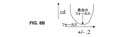
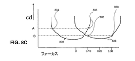
前記第1のウェーハに転写された前記第1のテスト構造および前記第2のテスト構造を測定し、測定結果と前記第1のテスト構造のフォーカス応答曲線および前記第2のテスト構造のフォーカス応答曲線とに基づき、少なくとも1つのリソグラフィプロセスパラメータの変化の方向を決定することと、
前記リソグラフィプロセスが変化したときに、前記少なくとも1つのリソグラフィプロセスパラメータを調整すること
を含む方法。 - 請求項1に記載の方法であって、
前記参照寸法は、前記第1のウェーハと第2のウェーハとの一方上に形成される前記ウェーハテスト構造の少なくとも一部の測定により得られる、方法。 - 請求項1に記載の方法であって、前記波面エンジニアリングフィーチャの設計は、前記ウェーハテスト構造の、前記少なくとも1つのリソグラフィプロセスパラメータの変化に対する最適化された感度を生むように選択される方法。
- 請求項1に記載の方法であって、前記波面エンジニアリングフィーチャの設計を実験的な手法で決定することをさらに含む方法。
- 請求項1に記載の方法であって、シミュレーションツール上で実行されるシミュレーションによって前記波面エンジニアリングフィーチャの設計を決定することをさらに含む方法。
- 請求項2に記載の方法であって、光学的オーバレイツールが用いられることによって、前記ウェーハテスト構造が測定される方法。
- 請求項1に記載の方法であって、前記波面エンジニアリングフィーチャの設計は、前記テスト構造が、前記ウェーハテスト構造を形成するのに用いられる露光ツールのフォーカスおよび露光量の変化に対して感度を持つように選択される方法。
- 請求項2に記載の方法であって、前記ウェーハテスト構造は、画像処理ソフトウェアを用いて分析される方法。
- 請求項1に記載の方法であって、前記波面エンジニアリングフィーチャは位相シフトマスクデザインである方法。
- 請求項1に記載の方法であって、前記波面エンジニアリングフィーチャは、光学近接補正である方法。
- 請求項1に記載の方法であって、前記テスト構造は、フォーカスおよび露光量変化に対して独立に応答する方法。
- 半導体プロセスパラメータを制御する方法であって、
第1のテスト構造および第2のテスト構造を持つパターンをレチクル上に形成すること、および
前記第1のテスト構造および前記第2のテスト構造のそれぞれに近接して互いに異なる波面エンジニアリングフィーチャを配置することによって、リソグラフィプロセスにおいて前記第1のテスト構造および前記第2のテスト構造の転写を制御すること
を含み、
前記第1のテスト構造および前記第2のテスト構造は、デュアルトーンラインショートニングアレイを備え、
前記波面エンジニアリングフィーチャは、前記パターンが複数のウェーハ上に転写されるとき、前記パターンのうちの前記第1のテスト構造部分および前記第2のテスト構造部分がプロセス変化に対して予め選択された感度であるように構成され、
前記方法は、さらに、
前記パターンの前記第1のテスト構造部分がフォーカスが合い前記第2のテスト構造部分がフォーカスがずれた状態でウェーハ上に前記パターンを形成すること、
前記ウェーハ上に形成された前記パターンの前記アレイ部分を測定することによって、ウェーハ上の前記パターンの他の形成に比較して前記プロセスが変化したかを決定すること、
前記ウェーハ上に形成された前記パターンの前記第1のテスト構造部分および前記第2のテスト構造部分を測定し、測定結果と前記第1のテスト構造のフォーカス応答曲線および前記第2のテスト構造のフォーカス応答曲線とに基づき、少なくとも1つのプロセスパラメータの変化の方向を決定すること、および
前記プロセスパラメータをそれらが変化したときに調整すること、を含む
方法。 - 請求項12に記載の方法であって、前記テスト構造は、前記リソグラフィプロセスのフォーカスおよび露光量変化に対して独立に応答する方法。
- 請求項12に記載の方法であって、前記パターンの前記形成および前記パターンの他の形成は、同じウェーハ上に起こる方法。
- 請求項12に記載の方法であって、前記波面エンジニアリングフィーチャは光学近接補正フィーチャであり、前記レチクル上に現れる前記テスト構造をフォーカスがずれた状態で転写させることによって、ウェーハ上に前記パターンを転写するのに用いられる露光ツールのフォーカスの変化の向きを決定するように前記波面エンジニアリングフィーチャがさらに構成される方法。
- 請求項15に記載の方法であって、前記テスト構造はデュアルトーンラインショートニングアレイを備え、前記光学近接補正フィーチャは、前記アレイに対して非対称に適用される方法。
- 半導体プロセスパラメータを制御する方法であって、
第1のテスト構造および第2のテスト構造を持つパターンをレチクル上に形成すること、および
ウェーハ上に転写された前記パターンのラインエンドショートニングを位相シフト技術を用いて制御することによって前記パターンのウェーハ上への転写を制御すること
を含み、
前記位相シフト技術は、前記パターンが複数のウェーハ上に転写されるとき、前記パターンがプロセス変化に対して感度を持つように選択され、
前記方法は、さらに、
前記パターンの前記第1のテスト構造部分がフォーカスが合い前記第2のテスト構造部分がフォーカスがずれた状態でウェーハ上に前記パターンを形成すること、
前記ウェーハ上の前記形成されたパターンを測定することによって、ウェーハ上の前記パターンの他の形成に比較して前記プロセスが変化したかを決定すること、
前記ウェーハ上に形成された前記パターンの前記第1のテスト構造部分および前記第2のテスト構造部分を測定し、測定結果と前記第1のテスト構造のフォーカス応答曲線および前記第2のテスト構造のフォーカス応答曲線とに基づき、少なくとも1つのプロセスパラメータの変化の方向を決定すること、および
前記プロセスパラメータをそれらが変化したときに調整すること、を含む
方法。 - 請求項17に記載の方法であって、前記位相シフト技術は、プロセス変化に対する予め選択された感度を生むよう選択される方法。
- 請求項17に記載の方法であって、前記位相シフト技術は、プロセス変化に対する高められた感度を生むよう選択される方法。
- 請求項17に記載の方法であって、前記位相シフト技術は、プロセス変化に対する低められた感度を生むよう選択される方法。
- 請求項1に記載の方法であって、
前記測定した部分が前記参照寸法を所定の閾値分超える場合に、前記リソグラフィプロセスパラメータを調整することをさらに含む、方法。 - 請求項1に記載の方法であって、
前記波面エンジニアリングフィーチャは、前記少なくとも1つのリソグラフィプロセスパラメータが所定の閾値分変化するとき、前記ウェーハテスト構造に所定の変化を引き起こすように構成されている、方法。
Applications Claiming Priority (5)
| Application Number | Priority Date | Filing Date | Title |
|---|---|---|---|
| US33571201P | 2001-11-14 | 2001-11-14 | |
| US60/335,712 | 2001-11-14 | ||
| US10/058,572 | 2002-01-28 | ||
| US10/058,572 US6673638B1 (en) | 2001-11-14 | 2002-01-28 | Method and apparatus for the production of process sensitive lithographic features |
| PCT/US2002/036819 WO2003043075A1 (en) | 2001-11-14 | 2002-11-14 | Method and apparatus for the production of process sensitive lithographic features |
Publications (3)
| Publication Number | Publication Date |
|---|---|
| JP2005510058A JP2005510058A (ja) | 2005-04-14 |
| JP2005510058A5 JP2005510058A5 (ja) | 2006-02-16 |
| JP5013657B2 true JP5013657B2 (ja) | 2012-08-29 |
Family
ID=26737761
Family Applications (1)
| Application Number | Title | Priority Date | Filing Date |
|---|---|---|---|
| JP2003544809A Expired - Fee Related JP5013657B2 (ja) | 2001-11-14 | 2002-11-14 | 半導体プロセスパラメータを制御する方法 |
Country Status (3)
| Country | Link |
|---|---|
| US (1) | US6673638B1 (ja) |
| JP (1) | JP5013657B2 (ja) |
| WO (1) | WO2003043075A1 (ja) |
Families Citing this family (88)
| Publication number | Priority date | Publication date | Assignee | Title |
|---|---|---|---|---|
| JP2003142376A (ja) * | 2001-11-02 | 2003-05-16 | Canon Inc | リソグラフィシステム、露光装置及びそれらの制御方法並びにデバイスの製造方法 |
| KR100434110B1 (ko) * | 2002-06-04 | 2004-06-04 | 삼성전자주식회사 | 반도체 장치의 제조방법 |
| US6711732B1 (en) * | 2002-07-26 | 2004-03-23 | Taiwan Semiconductor Manufacturing Company | Full sized scattering bar alt-PSM technique for IC manufacturing in sub-resolution era |
| JP4302965B2 (ja) * | 2002-11-01 | 2009-07-29 | 株式会社日立ハイテクノロジーズ | 半導体デバイスの製造方法及びその製造システム |
| US6746882B1 (en) * | 2002-11-21 | 2004-06-08 | Advanced Micro Devices, Inc. | Method of correcting non-linearity of metrology tools, and system for performing same |
| US7042550B2 (en) * | 2002-11-28 | 2006-05-09 | Asml Netherlands B.V. | Device manufacturing method and computer program |
| US7352453B2 (en) * | 2003-01-17 | 2008-04-01 | Kla-Tencor Technologies Corporation | Method for process optimization and control by comparison between 2 or more measured scatterometry signals |
| US7778721B2 (en) * | 2003-01-27 | 2010-08-17 | Applied Materials, Inc. | Small lot size lithography bays |
| US7221993B2 (en) * | 2003-01-27 | 2007-05-22 | Applied Materials, Inc. | Systems and methods for transferring small lot size substrate carriers between processing tools |
| WO2004099874A1 (ja) * | 2003-04-16 | 2004-11-18 | Nikon Corporation | パターン決定方法及びシステム、マスクの製造方法、結像性能調整方法、露光方法及び装置、並びにプログラム及び情報記録媒体 |
| US6968253B2 (en) * | 2003-05-07 | 2005-11-22 | Kla-Tencor Technologies Corp. | Computer-implemented method and carrier medium configured to generate a set of process parameters for a lithography process |
| CN1902501B (zh) * | 2003-07-17 | 2010-06-09 | 凸版光掩膜公司 | 校准计量工具的方法和装置 |
| US7218983B2 (en) | 2003-11-06 | 2007-05-15 | Applied Materials, Inc. | Method and apparatus for integrating large and small lot electronic device fabrication facilities |
| US7720557B2 (en) * | 2003-11-06 | 2010-05-18 | Applied Materials, Inc. | Methods and apparatus for enhanced operation of substrate carrier handlers |
| JP2005202102A (ja) * | 2004-01-15 | 2005-07-28 | Fujitsu Ltd | 露光用マスク及びそのパターン補正方法並びに半導体装置の製造方法 |
| US7274971B2 (en) | 2004-02-28 | 2007-09-25 | Applied Materials, Inc. | Methods and apparatus for electronic device manufacturing system monitoring and control |
| US7177716B2 (en) | 2004-02-28 | 2007-02-13 | Applied Materials, Inc. | Methods and apparatus for material control system interface |
| US7413069B2 (en) * | 2004-02-28 | 2008-08-19 | Applied Materials, Inc. | Methods and apparatus for transferring a substrate carrier within an electronic device manufacturing facility |
| US7146599B2 (en) * | 2004-04-15 | 2006-12-05 | Taiwan Semiconductor Manufacturing Co., Ltd. | Method for using asymmetric OPC structures on line ends of semiconductor pattern layers |
| TWI333233B (en) * | 2004-06-10 | 2010-11-11 | Applied Materials Inc | Small lot size lithography bays |
| US7369697B2 (en) * | 2004-06-17 | 2008-05-06 | Intel Corporation | Process variable of interest monitoring and control |
| US7052921B1 (en) * | 2004-09-03 | 2006-05-30 | Advanced Micro Devices, Inc. | System and method using in situ scatterometry to detect photoresist pattern integrity during the photolithography process |
| US7251807B2 (en) * | 2005-02-24 | 2007-07-31 | Synopsys, Inc. | Method and apparatus for identifying a manufacturing problem area in a layout using a process-sensitivity model |
| US7814456B2 (en) * | 2004-11-22 | 2010-10-12 | Tela Innovations, Inc. | Method and system for topography-aware reticle enhancement |
| JP4389222B2 (ja) * | 2005-05-02 | 2009-12-24 | エルピーダメモリ株式会社 | マスクデータ作成方法 |
| US7519940B2 (en) * | 2005-05-02 | 2009-04-14 | Cadence Design Systems, Inc. | Apparatus and method for compensating a lithography projection tool |
| US7536670B2 (en) * | 2005-05-31 | 2009-05-19 | Cadence Design Systems, Inc. | Method for verifying and choosing lithography model |
| US7392502B2 (en) * | 2005-06-30 | 2008-06-24 | Invarium, Inc. | Method for real time monitoring and verifying optical proximity correction model and method |
| US7695876B2 (en) * | 2005-08-31 | 2010-04-13 | Brion Technologies, Inc. | Method for identifying and using process window signature patterns for lithography process control |
| US7502702B1 (en) * | 2005-09-07 | 2009-03-10 | Advanced Micro Devices, Inc. | Method and apparatus for dynamic adjustment of sensor and/or metrology sensitivities |
| US7176675B1 (en) * | 2005-11-29 | 2007-02-13 | International Business Machines Corporation | Proximity sensitive defect monitor |
| US7506285B2 (en) | 2006-02-17 | 2009-03-17 | Mohamed Al-Imam | Multi-dimensional analysis for predicting RET model accuracy |
| US8541879B2 (en) | 2007-12-13 | 2013-09-24 | Tela Innovations, Inc. | Super-self-aligned contacts and method for making the same |
| US8658542B2 (en) | 2006-03-09 | 2014-02-25 | Tela Innovations, Inc. | Coarse grid design methods and structures |
| US8653857B2 (en) | 2006-03-09 | 2014-02-18 | Tela Innovations, Inc. | Circuitry and layouts for XOR and XNOR logic |
| US9035359B2 (en) | 2006-03-09 | 2015-05-19 | Tela Innovations, Inc. | Semiconductor chip including region including linear-shaped conductive structures forming gate electrodes and having electrical connection areas arranged relative to inner region between transistors of different types and associated methods |
| US9230910B2 (en) | 2006-03-09 | 2016-01-05 | Tela Innovations, Inc. | Oversized contacts and vias in layout defined by linearly constrained topology |
| US8225261B2 (en) * | 2006-03-09 | 2012-07-17 | Tela Innovations, Inc. | Methods for defining contact grid in dynamic array architecture |
| US8448102B2 (en) * | 2006-03-09 | 2013-05-21 | Tela Innovations, Inc. | Optimizing layout of irregular structures in regular layout context |
| US9563733B2 (en) * | 2009-05-06 | 2017-02-07 | Tela Innovations, Inc. | Cell circuit and layout with linear finfet structures |
| US7932545B2 (en) | 2006-03-09 | 2011-04-26 | Tela Innovations, Inc. | Semiconductor device and associated layouts including gate electrode level region having arrangement of six linear conductive segments with side-to-side spacing less than 360 nanometers |
| US8225239B2 (en) * | 2006-03-09 | 2012-07-17 | Tela Innovations, Inc. | Methods for defining and utilizing sub-resolution features in linear topology |
| US8839175B2 (en) | 2006-03-09 | 2014-09-16 | Tela Innovations, Inc. | Scalable meta-data objects |
| US7446352B2 (en) * | 2006-03-09 | 2008-11-04 | Tela Innovations, Inc. | Dynamic array architecture |
| US7908578B2 (en) * | 2007-08-02 | 2011-03-15 | Tela Innovations, Inc. | Methods for designing semiconductor device with dynamic array section |
| US7763534B2 (en) | 2007-10-26 | 2010-07-27 | Tela Innovations, Inc. | Methods, structures and designs for self-aligning local interconnects used in integrated circuits |
| US9009641B2 (en) | 2006-03-09 | 2015-04-14 | Tela Innovations, Inc. | Circuits with linear finfet structures |
| US7956421B2 (en) * | 2008-03-13 | 2011-06-07 | Tela Innovations, Inc. | Cross-coupled transistor layouts in restricted gate level layout architecture |
| US7943967B2 (en) * | 2006-03-09 | 2011-05-17 | Tela Innovations, Inc. | Semiconductor device and associated layouts including diffusion contact placement restriction based on relation to linear conductive segments |
| US8245180B2 (en) * | 2006-03-09 | 2012-08-14 | Tela Innovations, Inc. | Methods for defining and using co-optimized nanopatterns for integrated circuit design and apparatus implementing same |
| US8247846B2 (en) * | 2006-03-09 | 2012-08-21 | Tela Innovations, Inc. | Oversized contacts and vias in semiconductor chip defined by linearly constrained topology |
| US7925486B2 (en) | 2006-03-14 | 2011-04-12 | Kla-Tencor Technologies Corp. | Computer-implemented methods, carrier media, and systems for creating a metrology target structure design for a reticle layout |
| US7743357B2 (en) * | 2006-05-31 | 2010-06-22 | Synopsys, Inc. | Method and apparatus for determining a process model that models the impact of CAR/PEB on the resist profile |
| US7979829B2 (en) | 2007-02-20 | 2011-07-12 | Tela Innovations, Inc. | Integrated circuit cell library with cell-level process compensation technique (PCT) application and associated methods |
| US8286107B2 (en) * | 2007-02-20 | 2012-10-09 | Tela Innovations, Inc. | Methods and systems for process compensation technique acceleration |
| US8667443B2 (en) | 2007-03-05 | 2014-03-04 | Tela Innovations, Inc. | Integrated circuit cell library for multiple patterning |
| US7687206B2 (en) * | 2007-03-08 | 2010-03-30 | United Microelectronics Corp. | Mask pattern and method for forming the same |
| US20080241708A1 (en) * | 2007-04-02 | 2008-10-02 | Taiwan Semiconductor Manufacturing Company, Ltd. | Sub-resolution assist feature of a photomask |
| US7873504B1 (en) | 2007-05-07 | 2011-01-18 | Kla-Tencor Technologies Corp. | Computer-implemented methods, carrier media, and systems for creating a metrology target structure design for a reticle layout |
| US8453094B2 (en) | 2008-01-31 | 2013-05-28 | Tela Innovations, Inc. | Enforcement of semiconductor structure regularity for localized transistors and interconnect |
| US7939443B2 (en) | 2008-03-27 | 2011-05-10 | Tela Innovations, Inc. | Methods for multi-wire routing and apparatus implementing same |
| KR101739709B1 (ko) | 2008-07-16 | 2017-05-24 | 텔라 이노베이션스, 인코포레이티드 | 동적 어레이 아키텍쳐에서의 셀 페이징과 배치를 위한 방법 및 그 구현 |
| US9122832B2 (en) * | 2008-08-01 | 2015-09-01 | Tela Innovations, Inc. | Methods for controlling microloading variation in semiconductor wafer layout and fabrication |
| US8214771B2 (en) | 2009-01-08 | 2012-07-03 | Kla-Tencor Corporation | Scatterometry metrology target design optimization |
| US8661392B2 (en) | 2009-10-13 | 2014-02-25 | Tela Innovations, Inc. | Methods for cell boundary encroachment and layouts implementing the Same |
| US8453076B2 (en) * | 2010-03-16 | 2013-05-28 | International Business Machines Corporation | Wavefront engineering of mask data for semiconductor device design |
| US9159627B2 (en) | 2010-11-12 | 2015-10-13 | Tela Innovations, Inc. | Methods for linewidth modification and apparatus implementing the same |
| WO2012097833A1 (en) | 2011-01-20 | 2012-07-26 | Carl Zeiss Smt Gmbh | Method of operating a projection exposure tool |
| US10769320B2 (en) | 2012-12-18 | 2020-09-08 | Kla-Tencor Corporation | Integrated use of model-based metrology and a process model |
| US10274839B2 (en) * | 2013-03-11 | 2019-04-30 | Taiwan Semiconductor Manufacturing Company, Ltd. | Two-dimensional marks |
| US9448343B2 (en) | 2013-03-15 | 2016-09-20 | Kla-Tencor Corporation | Segmented mirror apparatus for imaging and method of using the same |
| US10101670B2 (en) | 2013-03-27 | 2018-10-16 | Kla-Tencor Corporation | Statistical model-based metrology |
| US9875946B2 (en) | 2013-04-19 | 2018-01-23 | Kla-Tencor Corporation | On-device metrology |
| US9383661B2 (en) | 2013-08-10 | 2016-07-05 | Kla-Tencor Corporation | Methods and apparatus for determining focus |
| US10935893B2 (en) | 2013-08-11 | 2021-03-02 | Kla-Tencor Corporation | Differential methods and apparatus for metrology of semiconductor targets |
| US9490182B2 (en) | 2013-12-23 | 2016-11-08 | Kla-Tencor Corporation | Measurement of multiple patterning parameters |
| WO2016083076A1 (en) | 2014-11-26 | 2016-06-02 | Asml Netherlands B.V. | Metrology method, computer product and system |
| KR102323388B1 (ko) | 2015-05-15 | 2021-11-05 | 케이엘에이 코포레이션 | 초점 감응성 오버레이 타겟을 이용한 초점 결정용 시스템 및 방법 |
| US10216096B2 (en) | 2015-08-14 | 2019-02-26 | Kla-Tencor Corporation | Process-sensitive metrology systems and methods |
| JP2017053674A (ja) | 2015-09-08 | 2017-03-16 | 株式会社ニューフレアテクノロジー | パターン幅寸法のずれ量測定方法及びパターン検査装置 |
| US20170256465A1 (en) | 2016-03-01 | 2017-09-07 | Asml Netherlands B.V. | Method and apparatus to determine a patterning process parameter |
| US9711420B1 (en) * | 2016-03-14 | 2017-07-18 | Taiwan Semiconductor Manufacturing Co., Ltd. | Inline focus monitoring |
| KR102450492B1 (ko) * | 2016-10-21 | 2022-09-30 | 에이에스엠엘 네델란즈 비.브이. | 패터닝 프로세스용 보정 결정 방법 |
| US10209627B2 (en) | 2017-01-06 | 2019-02-19 | Kla-Tencor Corporation | Systems and methods for focus-sensitive metrology targets |
| US10133838B2 (en) * | 2017-01-30 | 2018-11-20 | Dongfang Jingyuan Electron Limited | Guided defect detection of integrated circuits |
| EP3396456A1 (en) * | 2017-04-25 | 2018-10-31 | ASML Netherlands B.V. | Method of monitoring and device manufacturing method |
| CN108957943B (zh) | 2017-05-22 | 2021-02-19 | 联华电子股份有限公司 | 形成布局图案的方法 |
| WO2020141040A1 (en) * | 2019-01-03 | 2020-07-09 | Asml Netherlands B.V. | Methods and patterning devices and apparatuses for measuring focus performance of a lithographic apparatus, device manufacturing method |
Family Cites Families (23)
| Publication number | Priority date | Publication date | Assignee | Title |
|---|---|---|---|---|
| US4855253A (en) * | 1988-01-29 | 1989-08-08 | Hewlett-Packard | Test method for random defects in electronic microstructures |
| US5103557A (en) * | 1988-05-16 | 1992-04-14 | Leedy Glenn J | Making and testing an integrated circuit using high density probe points |
| US5682323A (en) * | 1995-03-06 | 1997-10-28 | Lsi Logic Corporation | System and method for performing optical proximity correction on macrocell libraries |
| JP2917879B2 (ja) * | 1995-10-31 | 1999-07-12 | 日本電気株式会社 | フォトマスク及びその製造方法 |
| JP4180678B2 (ja) * | 1997-05-29 | 2008-11-12 | 株式会社東芝 | 露光方法 |
| JP3067695B2 (ja) * | 1997-06-06 | 2000-07-17 | 日本電気株式会社 | 投影露光装置の検査方法 |
| US5976740A (en) | 1997-08-28 | 1999-11-02 | International Business Machines Corporation | Process for controlling exposure dose or focus parameters using tone reversing pattern |
| US5970311A (en) * | 1997-10-31 | 1999-10-19 | Advanced Micro Devices | Method and structure for optimizing the performance of a semiconductor device having dense transistors |
| US6174741B1 (en) * | 1997-12-19 | 2001-01-16 | Siemens Aktiengesellschaft | Method for quantifying proximity effect by measuring device performance |
| JPH11233434A (ja) * | 1998-02-17 | 1999-08-27 | Nikon Corp | 露光条件決定方法、露光方法、露光装置、及びデバイスの製造方法 |
| US6174630B1 (en) * | 1998-03-03 | 2001-01-16 | Lsi Logic Corporation | Method of proximity correction with relative segmentation |
| JP2000124103A (ja) * | 1998-10-16 | 2000-04-28 | Sony Corp | 露光方法および露光装置 |
| US6374396B1 (en) * | 1998-12-04 | 2002-04-16 | Micron Technology, Inc. | Correction of field effects in photolithography |
| JP2000181045A (ja) * | 1998-12-10 | 2000-06-30 | Matsushita Electronics Industry Corp | パターン補正方法 |
| US6294397B1 (en) * | 1999-03-04 | 2001-09-25 | Advanced Micro Devices, Inc. | Drop-in test structure and abbreviated integrated circuit process flow for characterizing production integrated circuit process flow, topography, and equipment |
| US6345210B1 (en) * | 1999-03-08 | 2002-02-05 | Advanced Micro Devices, Inc. | Method of using critical dimension mapping to qualify a reticle used in integrated circuit fabrication |
| US6120953A (en) * | 1999-04-23 | 2000-09-19 | United Microelectronics Corp. | Method of optical proximity correction |
| US6143579A (en) * | 1999-04-26 | 2000-11-07 | Taiwan Semiconductor Manufacturing Ltd. | Efficient method for monitoring gate oxide damage related to plasma etch chamber processing history |
| US6444373B1 (en) * | 2000-06-16 | 2002-09-03 | Advanced Micro Devices, Inc. | Modification of mask layout data to improve mask fidelity |
| US6448099B1 (en) * | 2000-11-28 | 2002-09-10 | Advanced Micro Devices, Inc. | Method and apparatus for detecting voltage contrast in a semiconductor wafer |
| US6365422B1 (en) * | 2001-01-22 | 2002-04-02 | Advanced Micro Devices, Inc. | Automated variation of stepper exposure dose based upon across wafer variations in device characteristics, and system for accomplishing same |
| US6433878B1 (en) * | 2001-01-29 | 2002-08-13 | Timbre Technology, Inc. | Method and apparatus for the determination of mask rules using scatterometry |
| US6458605B1 (en) * | 2001-06-28 | 2002-10-01 | Advanced Micro Devices, Inc. | Method and apparatus for controlling photolithography overlay registration |
-
2002
- 2002-01-28 US US10/058,572 patent/US6673638B1/en not_active Expired - Lifetime
- 2002-11-14 JP JP2003544809A patent/JP5013657B2/ja not_active Expired - Fee Related
- 2002-11-14 WO PCT/US2002/036819 patent/WO2003043075A1/en active Application Filing
Also Published As
| Publication number | Publication date |
|---|---|
| WO2003043075A1 (en) | 2003-05-22 |
| JP2005510058A (ja) | 2005-04-14 |
| US6673638B1 (en) | 2004-01-06 |
Similar Documents
| Publication | Publication Date | Title |
|---|---|---|
| JP5013657B2 (ja) | 半導体プロセスパラメータを制御する方法 | |
| JP4954211B2 (ja) | 個別マスクエラーモデルを使用するマスク検証を行うシステムおよび方法 | |
| JP5371179B2 (ja) | フォトマスクのテストパターンイメージから印刷されたテストフィーチャーを用いるフォトリソグラフィ工程における焦点変化を測定するシステム及び方法 | |
| JP3972035B2 (ja) | 検査方法とデバイス製造方法 | |
| US7327436B2 (en) | Method for evaluating a local flare, correction method for a mask pattern, manufacturing method for a semiconductor device and a computer program product | |
| US7536670B2 (en) | Method for verifying and choosing lithography model | |
| CN1862385B (zh) | 使用测试特征检测光刻工艺中的焦点变化的系统和方法 | |
| TW201939174A (zh) | 用於處理度量衡資料、用於處理基板之圖案之變數及用於預測輪廓之方法及電腦程式產品 | |
| JP2002311564A (ja) | 散乱測定を用いてマスクルールを求めるための方法および装置 | |
| JP4057847B2 (ja) | リソグラフィ投影装置の較正方法、パターニング装置、及びデバイス製造方法 | |
| JP2006301631A (ja) | 向上したフォトリソグラフィ工程ウィンドーを提供するフォトマスク構造及びその製造方法 | |
| JP2017538155A (ja) | パターニングデバイストポグラフィ誘起位相を使用するための方法及び装置 | |
| TW201633003A (zh) | 使用圖案化裝置形貌誘導相位之方法及設備 | |
| KR101175341B1 (ko) | 리소그래피 시스템에서 조명기의 조도 프로파일을 결정하는 장치 및 그 제조방법 | |
| TWI604277B (zh) | 使用圖案化裝置形貌誘導相位之方法及設備 | |
| TWI623822B (zh) | 用以檢測基板的方法及電腦程式 | |
| TW201632984A (zh) | 使用圖案化裝置形貌誘導相位之方法及設備 | |
| TWI636317B (zh) | 使用圖案化裝置形貌誘導相位之方法、非暫時性電腦程式產品及製造半導體裝置之方法 | |
| TWI769625B (zh) | 用於判定量測配方之方法及相關裝置 | |
| TWI706233B (zh) | 用以判定關於藉由一微影程序形成之一基板上之一結構的一所關注特性之方法、圖案化器件、微影系統、及非暫時性電腦程式產品 | |
| JP2009239029A (ja) | リソグラフィ装置の評価方法および制御方法 | |
| JP2004200691A (ja) | レンズ系の特性決定のための方法およびマスク | |
| CN117882011A (zh) | 监测光刻过程的方法以及相关设备 |
Legal Events
| Date | Code | Title | Description |
|---|---|---|---|
| A621 | Written request for application examination |
Free format text: JAPANESE INTERMEDIATE CODE: A621 Effective date: 20051114 |
|
| A521 | Request for written amendment filed |
Free format text: JAPANESE INTERMEDIATE CODE: A523 Effective date: 20051220 |
|
| A131 | Notification of reasons for refusal |
Free format text: JAPANESE INTERMEDIATE CODE: A131 Effective date: 20090407 |
|
| A601 | Written request for extension of time |
Free format text: JAPANESE INTERMEDIATE CODE: A601 Effective date: 20090706 |
|
| A602 | Written permission of extension of time |
Free format text: JAPANESE INTERMEDIATE CODE: A602 Effective date: 20090713 |
|
| A521 | Request for written amendment filed |
Free format text: JAPANESE INTERMEDIATE CODE: A523 Effective date: 20091006 |
|
| A131 | Notification of reasons for refusal |
Free format text: JAPANESE INTERMEDIATE CODE: A131 Effective date: 20100907 |
|
| A601 | Written request for extension of time |
Free format text: JAPANESE INTERMEDIATE CODE: A601 Effective date: 20101203 |
|
| A602 | Written permission of extension of time |
Free format text: JAPANESE INTERMEDIATE CODE: A602 Effective date: 20101210 |
|
| A521 | Request for written amendment filed |
Free format text: JAPANESE INTERMEDIATE CODE: A523 Effective date: 20110303 |
|
| A131 | Notification of reasons for refusal |
Free format text: JAPANESE INTERMEDIATE CODE: A131 Effective date: 20120110 |
|
| A521 | Request for written amendment filed |
Free format text: JAPANESE INTERMEDIATE CODE: A523 Effective date: 20120406 |
|
| TRDD | Decision of grant or rejection written | ||
| A01 | Written decision to grant a patent or to grant a registration (utility model) |
Free format text: JAPANESE INTERMEDIATE CODE: A01 Effective date: 20120508 |
|
| A01 | Written decision to grant a patent or to grant a registration (utility model) |
Free format text: JAPANESE INTERMEDIATE CODE: A01 |
|
| A61 | First payment of annual fees (during grant procedure) |
Free format text: JAPANESE INTERMEDIATE CODE: A61 Effective date: 20120605 |
|
| FPAY | Renewal fee payment (event date is renewal date of database) |
Free format text: PAYMENT UNTIL: 20150615 Year of fee payment: 3 |
|
| R150 | Certificate of patent or registration of utility model |
Free format text: JAPANESE INTERMEDIATE CODE: R150 Ref document number: 5013657 Country of ref document: JP Free format text: JAPANESE INTERMEDIATE CODE: R150 |
|
| R250 | Receipt of annual fees |
Free format text: JAPANESE INTERMEDIATE CODE: R250 |
|
| R250 | Receipt of annual fees |
Free format text: JAPANESE INTERMEDIATE CODE: R250 |
|
| R250 | Receipt of annual fees |
Free format text: JAPANESE INTERMEDIATE CODE: R250 |
|
| R250 | Receipt of annual fees |
Free format text: JAPANESE INTERMEDIATE CODE: R250 |
|
| R250 | Receipt of annual fees |
Free format text: JAPANESE INTERMEDIATE CODE: R250 |
|
| R250 | Receipt of annual fees |
Free format text: JAPANESE INTERMEDIATE CODE: R250 |
|
| R250 | Receipt of annual fees |
Free format text: JAPANESE INTERMEDIATE CODE: R250 |
|
| LAPS | Cancellation because of no payment of annual fees |