JP5013657B2 - Method for controlling semiconductor process parameters - Google Patents
Method for controlling semiconductor process parameters Download PDFInfo
- Publication number
- JP5013657B2 JP5013657B2 JP2003544809A JP2003544809A JP5013657B2 JP 5013657 B2 JP5013657 B2 JP 5013657B2 JP 2003544809 A JP2003544809 A JP 2003544809A JP 2003544809 A JP2003544809 A JP 2003544809A JP 5013657 B2 JP5013657 B2 JP 5013657B2
- Authority
- JP
- Japan
- Prior art keywords
- test structure
- wafer
- focus
- pattern
- changes
- Prior art date
- Legal status (The legal status is an assumption and is not a legal conclusion. Google has not performed a legal analysis and makes no representation as to the accuracy of the status listed.)
- Expired - Fee Related
Links
Images


Classifications
-
- G—PHYSICS
- G03—PHOTOGRAPHY; CINEMATOGRAPHY; ANALOGOUS TECHNIQUES USING WAVES OTHER THAN OPTICAL WAVES; ELECTROGRAPHY; HOLOGRAPHY
- G03F—PHOTOMECHANICAL PRODUCTION OF TEXTURED OR PATTERNED SURFACES, e.g. FOR PRINTING, FOR PROCESSING OF SEMICONDUCTOR DEVICES; MATERIALS THEREFOR; ORIGINALS THEREFOR; APPARATUS SPECIALLY ADAPTED THEREFOR
- G03F7/00—Photomechanical, e.g. photolithographic, production of textured or patterned surfaces, e.g. printing surfaces; Materials therefor, e.g. comprising photoresists; Apparatus specially adapted therefor
- G03F7/70—Microphotolithographic exposure; Apparatus therefor
- G03F7/70483—Information management; Active and passive control; Testing; Wafer monitoring, e.g. pattern monitoring
- G03F7/70605—Workpiece metrology
- G03F7/70616—Monitoring the printed patterns
- G03F7/70625—Dimensions, e.g. line width, critical dimension [CD], profile, sidewall angle or edge roughness
-
- G—PHYSICS
- G03—PHOTOGRAPHY; CINEMATOGRAPHY; ANALOGOUS TECHNIQUES USING WAVES OTHER THAN OPTICAL WAVES; ELECTROGRAPHY; HOLOGRAPHY
- G03F—PHOTOMECHANICAL PRODUCTION OF TEXTURED OR PATTERNED SURFACES, e.g. FOR PRINTING, FOR PROCESSING OF SEMICONDUCTOR DEVICES; MATERIALS THEREFOR; ORIGINALS THEREFOR; APPARATUS SPECIALLY ADAPTED THEREFOR
- G03F7/00—Photomechanical, e.g. photolithographic, production of textured or patterned surfaces, e.g. printing surfaces; Materials therefor, e.g. comprising photoresists; Apparatus specially adapted therefor
- G03F7/70—Microphotolithographic exposure; Apparatus therefor
- G03F7/70483—Information management; Active and passive control; Testing; Wafer monitoring, e.g. pattern monitoring
- G03F7/70605—Workpiece metrology
- G03F7/70616—Monitoring the printed patterns
- G03F7/70641—Focus
Description
本発明は一般に、半導体ウェーハ上にプロセスに調節可能に敏感なリソグラフィフィーチャを作ることに関する。より具体的には本発明は、ウェーブフロントエンジニアリングを用いてターゲットを、ウェーハ上にレイヤを転写することを実現する装置におけるフォーカスおよび薬量のバラツキに敏感な半導体ウェーハ上に作る装置および方法に関する。 The present invention generally relates to making process-adjustable lithographic features on a semiconductor wafer. More specifically, the present invention relates to an apparatus and method for making a target on a semiconductor wafer that is sensitive to focus and dose variation in an apparatus that implements transferring a layer onto the wafer using wavefront engineering.
設計者および半導体デバイス製造者は、より小さいフィーチャを持つ回路が一般により速い速度および改善された歩留まり(標準的な半導体ウェーハから作られる使用可能なチップの数)を提供することを認識して、より小さいデバイスをウェーハから開発するために常に努めている。特にデバイス上に印刷される線幅については、一貫した寸法でウェーハを作ることが望まれる。しかしより小さいデバイス(転写されたフィーチャの微小寸法が露光波長より小さい)では、微小寸法の交差に適合する困難さが増す。ある種の光学近接効果補正(OPC)および位相シフトマスク(PSM)技術のような波面エンジニアリング技術はしばしばレチクルに応用されて、リソグラフィパフォーマンスを改善し、光学露光ツールの有効な寿命を延ばす。これらの技術によって作られた変化は、波面エンジニアリングと呼ばれる。位相シフトマスク(PSM)技術(強−交互、弱−埋め込み、および減衰)が主にリソグラフィ解像度を改善し、フォーカス深度を改善し、かつフォーカスモニタを用いてリソグラフィステッパまたはスキャナパフォーマンスをモニタする。光学近接効果補正は、マスクからウェーハへのパターン転写のあいだに起こるフィーチャ形状およびサイズの変化を補償するために、フォトマスクパターンの変更(バイナリチェンジ、すなわちマスク上でクロムを加算したり減算したりする)が行われる波面エンジニアリング技術である。これらのフィーチャの変化は、隣接リソグラフィフィーチャの存在、ウェーハステッパ/スキャナの限界、または与えられたウェーハプロセスステップの動作のバラツキによる過度の露光によって引き起こされえる。OPCはまた、位相シフトマスク上で用いられて、PSM技術からえられる優位性を最大限にする。OPC技術は、パターン忠実度エラー(空中からのイメージのクォリティの低下)について補正し、プロセスラチチュードを改善するのにしばしば用いられるが、OPCは解像度を改善するのには少ししか役立たない。OPCおよびPSM技術に加えて、さまざまな他の波面エンジニアリング技術が現在用いられる。例えば、「スキャッタバー」と呼ばれるサブ解像度フィーチャ(バイナリマスク追加または転写しないサブ解像度マスクパターン)は、空中イメージの形状を調整することー単にOPC技術を応用することーによって小さく分離され疑似的に密なフィーチャのリソグラフィ的なふるまいを改善する。 Designers and semiconductor device manufacturers recognize that circuits with smaller features generally provide faster speeds and improved yields (number of usable chips made from standard semiconductor wafers) We are constantly striving to develop smaller devices from wafers. In particular, for line widths printed on devices, it is desirable to make wafers with consistent dimensions. However, smaller devices (where the transferred feature micro-dimensions are smaller than the exposure wavelength) increase the difficulty of meeting micro-dimension crossings. Wavefront engineering techniques, such as certain optical proximity correction (OPC) and phase shift mask (PSM) techniques, are often applied to reticles to improve lithographic performance and extend the useful life of optical exposure tools. The changes made by these techniques are called wavefront engineering. Phase shift mask (PSM) technology (strong-alternating, weak-embedding, and attenuation) primarily improves lithography resolution, improves focus depth, and uses a focus monitor to monitor lithography stepper or scanner performance. Optical proximity correction is a photomask pattern change (binary change, ie adding or subtracting chrome on the mask) to compensate for feature shape and size changes that occur during mask-to-wafer pattern transfer. Wavefront engineering technology. These feature changes can be caused by overexposure due to the presence of adjacent lithographic features, wafer stepper / scanner limitations, or variations in the operation of a given wafer process step. OPC is also used on phase shift masks to maximize the advantages gained from PSM technology. Although OPC techniques are often used to correct for pattern fidelity errors (degradation of image quality from the air) and improve process latitude, OPC is only of little use to improve resolution. In addition to OPC and PSM technologies, various other wavefront engineering technologies are currently used. For example, sub-resolution features called “scatterbars” (sub-resolution mask patterns that do not add or transfer a binary mask) can be separated into small and pseudo-dense by adjusting the shape of the aerial image – simply by applying OPC technology. Improve the lithographic behavior of sensitive features.
フォトリソグラフィ露光装置(スキャナ/ステッパ)におけるフォーカスおよび露光量の変化のようなプロセスパラメータのマイナーなバラツキは、ウェーハ上の微小寸法が許容可能な半導体製造公差(典型的なCD仕様では+/−8%)の外に出ることを引き起こしえる。多くのプロセスパラメータがシリコンウェーハ上のレジストパターンの寸法に影響を与ええる。最も重要なパラメータには、レジストの厚さ、フォーカス位置、露光量、レジストのプリ・ポストベーク温度および現像温度および時間が含まれる。フォトリソグラフィ露光ツールおよびフォトリソグラフィレジストトラックは、プロセス条件(ベーク時間、露光量、フォーカスなど)の微小な変動する変化を連続的にモニタし調整するが、結果として生じるレジストフィーチャサイズまたは微小寸法は、全てのプロセス変数の複雑な結果である。典型的には半導体製造施設は、露光量(例えば時間的な変化)だけを調節することによってプロセスのバラツキ(ドリフトするCD)について補正する。これは、たいていの経済的に見て可能なソリューションを提供する傾向にある。 Minor variations in process parameters such as focus and exposure dose changes in photolithographic exposure apparatus (scanner / stepper) are due to semiconductor manufacturing tolerances that allow for small dimensions on the wafer (+/− 8 for typical CD specifications). %) Can cause you to go outside. Many process parameters can affect the size of the resist pattern on the silicon wafer. The most important parameters include resist thickness, focus position, exposure, resist pre / post bake temperature and development temperature and time. Photolithographic exposure tools and photolithographic resist tracks continuously monitor and adjust for minute and changing changes in process conditions (bake time, exposure dose, focus, etc.), but the resulting resist feature size or dimension is It is a complex result of all process variables. Typically, a semiconductor manufacturing facility corrects for process variations (drifting CD) by adjusting only the exposure dose (eg, changes over time). This tends to provide most economically viable solutions.
フォトリソグラフィは、半導体製造プロセスのうちで最も重要なステップのうちの一つである。フォトリソグラフィプロセスのあいだ、半導体ウェーハは、フォトレジストまたはレジスト(例:化学増幅レジスト(CAR))と呼ばれる感光性材料で覆われ、作用光源(エキシマレーザ、水銀ランプなど)で露光される。露光用光線は、フォトマスクを透過し、投影光学系を介してレジストで覆われたウェーハ上に結像され、フォトマスクの縮小されたイメージをフォトレジスト中に形成する(典型的には4倍または5倍に縮小)。ポジ化学増幅レジスト(CAR)については、作用光源は典型的には、ポスト露光ベークのあいだに拡散する光酸の発生を引き起こし、露光量のほとんどを受けた領域においてだけ水溶性現像液によってレジストが洗い流されることを許す。現像プロセスに続いて、レジストでパターンが付けられたウェーハは、計測ステーションに送られ、微小寸法またはパターン付けされたレジストフィーチャの形状が測定される。典型的な計測ツールには、散乱計、走査電子顕微鏡および原子間力顕微鏡が含まれる。フォトリソグラフィプロセスの最後のステップには、レジストで覆われたウェーハを複雑なプラズマ化学を用いてエッチングして、フォトレジストで覆われていない半導体材料を侵す。 Photolithography is one of the most important steps in the semiconductor manufacturing process. During the photolithography process, the semiconductor wafer is covered with a photosensitive material called photoresist or resist (eg, chemically amplified resist (CAR)) and exposed with a working light source (excimer laser, mercury lamp, etc.). The exposure beam passes through the photomask and is imaged onto the resist-covered wafer via the projection optics to form a reduced image of the photomask in the photoresist (typically 4 ×). Or reduced to 5 times). For positive chemically amplified resists (CARs), the working light source typically causes the generation of photoacids that diffuse during post-exposure baking, so that the resist is removed by the aqueous developer only in the areas that have received most of the exposure. Allow to be washed away. Following the development process, the resist-patterned wafer is sent to a metrology station where the dimensions of the micro-sized or patterned resist features are measured. Typical metrology tools include scatterometers, scanning electron microscopes and atomic force microscopes. In the final step of the photolithography process, the resist-covered wafer is etched using complex plasma chemistry to attack the semiconductor material not covered by the photoresist.
エッチングに続いて、レジストで覆われたウェーハは洗浄され、走査電子顕微鏡または他の計測器に送られ、最終的なリソグラフィ検査が行われる。転写プロセスの正確な制御が、ウェーハ上のパターンを形成するデバイス線幅が公差内に入ることを確実にするために必要である。もし問題が間に合って検出されるなら、エッチングの前にリソグラフィプロセスを繰り返すことが可能である。フォトレジストウェーハが物理的にエッチングされた後なら、フォトリソグラフィイメージングプロセスを修正するには遅すぎる。現在は、用いられる一つのモニタリング技術は、エッチング前に線幅(微小寸法)が許容可能な範囲の外に落ちていないかを決定するために、レジストでイメージされたウェーハのロットサンプリングである。しかしデバイスのサイズが極端に小さいことから、例えばデバイスサイズが0.15μm以下であることから、高価で遅い計測技術が必要である。これらの寸法で、線幅を測定するのに現在用いられる数少ない効果的なツールの一つは、走査電子顕微鏡(SEM)である。ウェーハは、そのプロセス位置から取り出されて、SEMに搬送されなければならない。さらにSEM検査に必要とされる時間は非常に長いので、典型的なサンプリングレートでは、大量のウェーハがエッチングされた後でなければプロセスドリフトを検出できない。 Following etching, the resist-covered wafer is cleaned and sent to a scanning electron microscope or other instrument for final lithography inspection. Accurate control of the transfer process is necessary to ensure that the device line width forming the pattern on the wafer is within tolerance. If a problem is detected in time, the lithography process can be repeated before etching. Once the photoresist wafer has been physically etched, it is too late to modify the photolithography imaging process. Currently, one monitoring technique that is used is lot sampling of resist imaged wafers to determine if the line width (minor dimension) has fallen outside of an acceptable range prior to etching. However, since the device size is extremely small, for example, the device size is 0.15 μm or less, an expensive and slow measurement technique is required. With these dimensions, one of the few effective tools currently used to measure line width is the scanning electron microscope (SEM). The wafer must be removed from its process location and transferred to the SEM. In addition, the time required for SEM inspection is so long that typical sampling rates can detect process drift only after a large number of wafers have been etched.
他のモニタリング計測には、複雑で高価なルックアップライブラリを用いる散乱計測技術(エリプソメトリ、可変角、反射)、および安価な光学計測ツールおよびラインエンド短絡技術を用いるフォトレジストパターン付きウェーハの微小寸法を間接に測定するためのデュアルトーンライン短絡(「シュニッツェル」)アレイを利用する光学CD技術が含まれる。OCD技術は高速で安価であるが、この技術は、日々の製造モニタリングルーチンに必要とされる最適なプロセス感度を持つかもしれず持たないかもしれない。実際にはOCD技術は、フォーカスおよび露光の変化についての複雑なCDドリフトの2次多項式記述を構築することによってフォーカスおよび露光ドリフトの両方を決定するのに用いられえる。しかしフォーカスドリフトの絶対的な方向を決定する能力は、フォーカスがずれたテストフィールドのさらなる転写を要求する。これは高価な露光時間および半導体ウェーハ上のスペースが必要となる。 Other monitoring measurements include scatterometry techniques (ellipsometry, variable angle, reflection) using complex and expensive look-up libraries, and photoresist patterned wafer micro-dimensions using inexpensive optical metrology tools and line-end short-circuit techniques Includes optical CD technology that utilizes a dual tone line short circuit ("Schnitzel") array to indirectly measure. Although OCD technology is fast and inexpensive, this technology may or may not have the optimum process sensitivity required for daily manufacturing monitoring routines. In practice, OCD techniques can be used to determine both focus and exposure drift by building a second order polynomial description of complex CD drift for focus and exposure changes. However, the ability to determine the absolute direction of focus drift requires further transfer of the defocused test field. This requires expensive exposure time and space on the semiconductor wafer.
必要となるのは、プロセス感度の調整可能なレベルを持ち、フォーカスドリフトの方向を予測できる光学計測技術を用いて半導体プロセスにおけるバラツキを検出する迅速で安価な方法である。 What is needed is a fast and inexpensive method of detecting variations in semiconductor processes using optical metrology techniques that have adjustable levels of process sensitivity and can predict the direction of focus drift.
前述を達成するために、本発明の目的によれば、フォトリソグラフィプロセスパラメータをより多目的に効率的にモニタリングおよび制御する方法が説明される。 In order to achieve the foregoing, according to the objects of the present invention, a method for more efficiently and efficiently monitoring and controlling photolithography process parameters is described.
本発明は、プロセス感度の調整可能な程度を持ち、フォーカスドリフトの絶対的な向きを決定するのに用いられえる変更されたターゲット構造を用いてプロセスパラメータの変動を制御する方法を提供する。マスクレベルデュアルトーンペアラインショートニングテスト構造(例えば「シュニッツェルアレイ」)を変更するために光学近接補正および/またはPSM技術が用いられて、CD対フォーカスおよび露光量プロセス感度をカスタマイズする。変更されたシュニッツェルアレイテスト構造は、ウェーハ上の選択された位置において転写され、半導体リソグラフィプロセスをモニタするのに用いられる。もしプロセスが変化するなら、フォーカスおよび露光量パラメータはテスト構造の測定値に応答して調整されえる。 The present invention provides a method of controlling process parameter variations using a modified target structure that has an adjustable degree of process sensitivity and can be used to determine the absolute orientation of focus drift. Optical proximity correction and / or PSM techniques are used to modify the mask level dual tone pair line shortening test structure (e.g., "Schnitzel array") to customize CD versus focus and dose process sensitivity. The modified schnitzel array test structure is transferred at selected locations on the wafer and used to monitor the semiconductor lithography process. If the process changes, focus and exposure parameters can be adjusted in response to test structure measurements.
ある局面において、半導体プロセスパラメータを制御する方法は、テスト構造を持つパターンをレチクル上に形成すること、および波面エンジニアリングフィーチャを利用して前記レチクル上に現れる前記テスト構造の転写特性を変更することによって、リソグラフィプロセス変化に対する前記テスト構造の感度を調整することを含む。 In one aspect, a method for controlling semiconductor process parameters includes forming a pattern with a test structure on a reticle, and utilizing wavefront engineering features to alter the transfer characteristics of the test structure that appear on the reticle. Adjusting the sensitivity of the test structure to lithographic process changes.
他の局面において、光学近接補正または位相シフトマスクフィーチャが配置され、フォーカスおよび露光量プロセス変化を区別できるテスト構造を変更する。波面エンジニアリングフィーチャは、ターゲット構造の感度が調整されることを可能にする。この感度はプロセスをモニタするのに用いられ、すなわちフォトリソグラフィツールのフォーカスまたは露光量が変化したかを決定するのに用いられる。 In other aspects, optical proximity correction or phase shift mask features are placed to modify the test structure that can distinguish between focus and dose process changes. Wavefront engineering features allow the sensitivity of the target structure to be adjusted. This sensitivity is used to monitor the process, i.e. to determine if the focus or exposure of the photolithography tool has changed.
他の局面において、波面エンジニアリングフィーチャは、非対称的に配置されたOPCフィーチャであり、これによりプロセスフォーカス変化の向きおよび大きさについての決定が可能になる。 In other aspects, the wavefront engineering features are asymmetrically placed OPC features that allow determination of the direction and magnitude of process focus changes.
本発明のこれらおよび他の特徴および優位性は、本発明の以下の説明および添付図面においてより詳細に示され、これらは本発明の原理を例示的に示す。 These and other features and advantages of the present invention are shown in greater detail in the following description of the invention and the accompanying drawings, which illustrate, by way of example, the principles of the invention.
本発明は、以下の詳細な説明を添付の図面とあわせれば容易に理解され、ここで同様の参照番号は同様の構成要素を示す。 The present invention will be readily understood by the following detailed description in conjunction with the accompanying drawings, and like reference numerals designate like elements.
本発明の具体的な実施形態が詳細に参照される。これら実施形態の例は、添付図面において図示される。本発明はこれらの具体的な実施形態について説明されるが、本発明はこれらの実施形態に限定されるよう意図されていない。むしろ添付の特許請求の範囲によって規定されるように本発明の真の精神および範囲内に含まれるよう改変、変更、および等価物をカバーするように意図される。以下の記載においては、多くの具体的な詳細が本発明の完全な理解を与えるために述べられる。本発明はこれらの具体的な詳細の一部または全てがなくても実施できる。あるいは既知のプロセス操作は、本発明の本質を不必要にぼかさないために、詳細に記載されない。 Reference will now be made in detail to specific embodiments of the invention. Examples of these embodiments are illustrated in the accompanying drawings. While the invention will be described with reference to these specific embodiments, the invention is not intended to be limited to these embodiments. Rather, it is intended to cover modifications, changes, and equivalents as included within the true spirit and scope of the invention as defined by the appended claims. In the following description, numerous specific details are set forth in order to provide a thorough understanding of the present invention. The present invention may be practiced without some or all of these specific details. In other instances, known process operations have not been described in detail in order not to unnecessarily blur the essence of the invention.
図1は、レチクル上に現れるパターンのバイナリ変化の形状におけるさまざまな波面エンジニアリング技術の使用の概略図である。これらの変化は、ウェーハ上に転写されたパターンの寸法を制御する。図1は、アレイ100を構成するテスト構造フィーチャ102、104、106、108および110を持つレチクル上のOPC補正されたアレイ100を示す。セリフ(serifs)112は、テスト構造フィーチャ102に追加されることによって転写されたパターン上での角の丸みおよびフィーチャ長短縮を低減する。セリフ112は、サブ解像度補助フィーチャ、すなわちテスト構造フィーチャの転写されたウェーハ上への転写を制御するが、それら自身は転写されたテスト構造には現れないレチクル上に現れるフィーチャの例である。図1に示されるサブ解像度補助フィーチャの他の例には、ラインジョグ120および122と共にスキャッタリングバー114、116、および118が含まれる。
FIG. 1 is a schematic diagram of the use of various wavefront engineering techniques in the form of a binary variation of a pattern appearing on a reticle. These changes control the dimensions of the pattern transferred onto the wafer. FIG. 1 shows an OPC corrected
図1に示されるサブ解像度補助フィーチャ112〜122は、転写されたウェーハ上のラインエンド短縮効果を制御するよう構成されえる。ラインエンド短縮効果の量は、プロセスパラメータの変化に敏感である。プロセス変化によるラインエンド短縮効果を制御するために任意の適切なサブ解像度フィーチャが用いられえる。波面エンジニアリング技術は、例えばスキャッタリングバー、ハンマーヘッド、およびセリフを含むさまざまな形態のサブ解像度補助フィーチャを利用する。 The sub-resolution assist features 112-122 shown in FIG. 1 can be configured to control the line end shortening effect on the transferred wafer. The amount of line end shortening effect is sensitive to changes in process parameters. Any suitable sub-resolution feature can be used to control line end shortening effects due to process changes. Wavefront engineering techniques utilize various forms of sub-resolution assist features including, for example, scattering bars, hammerheads, and serifs.
波面エンジニアリング技術は、より多くのプロセスラチチュードを作り、それによりリソグラフィプロセスのプロセスウィンドウを改善する。この融通性によって転写された形状は、狭い公差の中に収められる。サブ解像度フィーチャは、波面補正のよく知られた原理を利用することによって、この結果を達成し、バイナリマスクおよび位相シフトマスクの両方において用いられえる。バイナリマスクにおいては、不透明な部分(典型的にはクロム)およびレチクルの透明な部分によって作られたパターンが用いられて、さまざまな技術を用いて露光されたウェーハ上にパターンを作る。位相シフトマスクは入射する露光ビームの位相をさらに操作することでウェーハ上のパターンの位置を特定する。レチクルは、当業者によってよく知られる技術にしたがって作られえる。 Wavefront engineering techniques create more process latitude, thereby improving the process window of the lithography process. Shapes transferred by this flexibility are accommodated within narrow tolerances. Sub-resolution features achieve this result by utilizing well-known principles of wavefront correction and can be used in both binary and phase shift masks. In a binary mask, a pattern created by opaque portions (typically chrome) and a transparent portion of the reticle is used to create a pattern on the exposed wafer using various techniques. The phase shift mask further specifies the position of the pattern on the wafer by further manipulating the phase of the incident exposure beam. The reticle can be made according to techniques well known by those skilled in the art.
たいていの典型的な応用例では、サブ解像度フィーチャは、プライマリパターンフィーチャ(すなわちウェーハ上に転写されることが望まれる回路のライン部分)の横に配置され、リソグラフィプロセスの露光ツールにおけるフォーカスまたは露光量(dosage)のドリフトのような、ウェーハフィーチャのプロセス制御における変化に対する感度を減らすのに用いられる。これはしばしば望まれることで、回路パターンはプロセスがドリフトするときであっても一貫して転写される。そうでなければ、ライン長における変化は回路に悪影響を与えうる。例えば、コンタクトは、長さが縮まった特定の導電ラインとは適切にアラインしなくなりえる。 In most typical applications, the sub-resolution feature is placed next to the primary pattern feature (ie, the line portion of the circuit that is desired to be transferred onto the wafer) and focused or exposed in the exposure tool of the lithography process. It is used to reduce sensitivity to changes in process control of wafer features, such as dose drift. This is often desirable and the circuit pattern is transferred consistently even when the process drifts. Otherwise, changes in line length can adversely affect the circuit. For example, a contact may not properly align with a particular conductive line of reduced length.
製品仕様はふつう、ライン幅のようなデバイス寸法のための許容可能な範囲つまり公差を提供する。用いられる極端に小さい寸法に適合することを確実にするために、高価で時間のかかる検査方法が従来用いられてきている。例えば完成したウェーハのサンプリングは、走査電子顕微鏡(SEM)によって検査される。SEM測定は、リソグラフィプロセスの初期セットアップにおける用いられるが、ポストパターニングSEMサンプリング検査は、従来のプロセスにおいて微小寸法が許容可能な限界の中に留まっていることを確実にするために必要であった。微小寸法は、プロセス変化のために変化しえる。 Product specifications usually provide an acceptable range or tolerance for device dimensions such as line width. Expensive and time consuming inspection methods have been used in the past to ensure that the extremely small dimensions used are met. For example, the sampling of a completed wafer is inspected by a scanning electron microscope (SEM). Although SEM measurements are used in the initial setup of the lithographic process, post-patterning SEM sampling inspection was necessary to ensure that small dimensions remained within acceptable limits in conventional processes. Small dimensions can change due to process changes.
理論上は高くされた感度はパターンありウェーハにおいて望ましくないが、製造中にフォーカスおよび露光量パラメータのドリフトをモニタするためには効果的に用いられえる。プロセスパラメータの変化、すなわち「プロセスウィンドウ」における変化は転写されたパターンにある程度、影響を与えるが、多くの場合はプロセスウィンドウにおける位置のシフトは、デバイスの微小寸法において小さな変化しか作りださない。この問題に対応するために、すなわちよりよくプロセス変化をモニタリングするために、デュアルトーンラインエンドショートニングアレイ(dual tone line end shortening array)のような専門のターゲット構造(例えばテスト構造)が従来、ウェーハ上の目立たない位置に転写するためのレチクル上に配置されてきた。これらのラインショートニングアレイは、プロセスパラメータ変化により感度が高く、ラインショートニングが光学測定ツールを用いて検出されることを可能にする。しかしプロセスウィンドウ内のある種のバラツキは、これらのラインエンドショートニングアレイおよび光学ツールを用いても容易には検出されえない。例えばプロセスウィンドウは、主にフォーカスおよび露光量の組み合わせとして特徴付けられえる。デュアルトーンアレイのようなテスト構造は、プロセスウィンドウからの大きな変動には敏感かもしれないが、初期に選択されたフォーカスおよび露光量からの小さなズレ、例えば数nmの範囲の+または−のフォーカスの変化は、デュアルトーンラインエンドショートニングアレイに応用される光学測定を用いては検出されないかもしれない。波面エンジニアリングのフィーチャをデュアルトーンアレイの近傍に配置することは、ある実施形態においては、デュアルトーンアレイまたは他のターゲット構造を、プロセスウィンドウのその部分における小さなプロセス変化に対してさえも敏感にさせ、よって光学測定ツールを用いて検出可能にする。 Theoretically increased sensitivity is undesirable in patterned wafers, but can be used effectively to monitor focus and dose parameter drift during manufacturing. Changes in process parameters, i.e. changes in the "process window", affect the transferred pattern to some extent, but in many cases a shift in position in the process window will produce only a small change in the device micro-dimension. To address this issue, ie to better monitor process changes, specialized target structures such as dual tone line end shortening arrays (eg test structures) have traditionally been on the wafer. It has been placed on a reticle for transferring to an inconspicuous position. These line shortening arrays are sensitive to process parameter changes and allow line shortening to be detected using optical measurement tools. However, certain variations within the process window cannot be easily detected using these line end shortening arrays and optical tools. For example, the process window can be characterized primarily as a combination of focus and exposure. Test structures such as dual tone arrays may be sensitive to large variations from the process window, but small deviations from the initially selected focus and exposure, eg, + or-focus in the range of a few nm. Changes may not be detected using optical measurements applied to dual tone line end shortening arrays. Placing wavefront engineering features in the vicinity of the dual tone array, in certain embodiments, makes the dual tone array or other target structure sensitive to even small process changes in that portion of the process window, Therefore, detection is possible using an optical measurement tool.
本発明は、微小寸法に悪影響も及ぼしえるプロセスの変化を直接にモニタリングする調整可能に敏感なテストターゲットを用いる方法を提供する。テストターゲットは、ウェーハフィーチャに相関のあるプロセスセンシティブなターゲットを用いて光学またはSEMツールを用いてプロセスをモニタするために測定されえる。プロセスは制御されるので、微小寸法もまた理想的に制御される。したがって微小寸法は製造後に独立して確認される必要はない。 The present invention provides a method using a tunable and sensitive test target that directly monitors process changes that can also adversely affect micro dimensions. The test target may be measured to monitor the process using an optical or SEM tool using a process sensitive target that is correlated to the wafer features. Since the process is controlled, the micro dimensions are also ideally controlled. Therefore, the minute dimensions need not be independently confirmed after manufacture.
前述のようにOPCおよびPSMのフィーチャは、典型的には、回路のパターン付きラインを、フォーカスおよび露光量のようなリソグラフィプロセスパラメータの変化により感度が低い転写されたウェーハ上に作るために用いられる。しかしOPCおよびPSMフィーチャの適切な選択(例えばそれらのサイズ、設計、および配置)を通して、パターン付きデバイスラインは、プロセス中のフォーカスおよび露光量に対するある程度の範囲を持った感度で作られえる。すなわち、フォーカスおよび露光量のバラツキが、所望の、または制御可能な範囲のラインエンドショートニングを作り、それによってプロセス変化のよりよいモニタリングを提供し、かつそれによってよりよいプロセス制御を可能にするように、OPCおよびPSMフィーチャは構成されえる。本発明の実施形態を用いて、ラインエンドショートニング技術およびOPCまたはPSMフィーチャを利用するテストターゲットまたはテストターゲットのアレイは、プロセス変化に対して最大の感度を持つように設計されえる。テストターゲットは、機能する回路の一部ではないので、プロセス変化への高められた反応は、回路の機能に悪影響を及ばさない。ラインエンドショートニングの量は、波面エンジニアリング技術を用いて調整されえる。 As noted above, OPC and PSM features are typically used to create patterned lines of circuitry on transferred wafers that are less sensitive to changes in lithography process parameters such as focus and exposure. . However, through appropriate selection of OPC and PSM features (eg, their size, design, and placement), patterned device lines can be made with a degree of sensitivity to in-process focus and exposure. That is, focus and exposure variability creates a desired or controllable range of line end shortening, thereby providing better monitoring of process changes and thereby allowing better process control , OPC and PSM features can be configured. Using embodiments of the present invention, test targets or arrays of test targets that utilize line end shortening techniques and OPC or PSM features can be designed to have maximum sensitivity to process changes. Since the test target is not part of the functioning circuit, the enhanced response to process changes will not adversely affect the functioning of the circuit. The amount of line end shortening can be adjusted using wavefront engineering techniques.
図1および図2A〜2Bは、本発明の実施形態によって、調整可能に感度を持つ転写されたリソグラフィフィーチャをウェーハ上に作るために用いられる波面エンジニアリング技術をさらに示す。図1のテスト構造フィーチャ102〜110によって実現されるアレイは、より感度の低いテスト構造フィーチャ(112および114と併せた102)から、より感度の高いテスト構造フィーチャ(122と併せた110)までの範囲を持つ。図2A〜2Bは、図1に示されるレチクルからのアレイ100を用いて形成されたダイ208を持つパターン付きウェーハ206におけるこの感度範囲を示す。図1のレチクル上に現れたサブ解像度フィーチャ112〜122は、図2A内のフィーチャされた転写パターン内に現れず、あるいは図2Bに示される転写パターンの拡大図にも現れず、しかしそれらの転写されたウェーハパターンへの影響は識別可能である。ラインエンドショートニング(線端後退)は、リソグラフィプロセスの物理学的および化学的な複雑な関数である。アレイを備えるテスト構造と共に用いられるとき、ラインエンドショートニングは、典型的には距離221(L)のような、アレイを構成する2本のフィーチャ間において測定される。転写されたライン210は、最小ラインエンドショートニングを示し、一方、ライン212〜218は徐々に大きくなるラインエンドショートニングを示す。
1 and 2A-2B further illustrate wavefront engineering techniques used to make tunably sensitive transferred lithographic features on a wafer in accordance with embodiments of the present invention. The array realized by the test structure features 102-110 of FIG. 1 ranges from the less sensitive test structure features (102 in combination with 112 and 114) to the more sensitive test structure features (110 in combination with 122). With a range. 2A-2B illustrate this sensitivity range for a
ラインエンドショートニングターゲットアレイの感度は、光学的近接および位相シフトマスク補正の構成および設計で変化する。より具体的には、プロセス変化に応答した選択されたラインエンドショートニングターゲット寸法の変化は、波面エンジニアリングフィーチャの設計と共に変化する。製品ウェーハ中のプロセスウィンドウ内の位置のシフトは、ウェーハ内にわたって、またはウェーハ群間で発生しえる。要するに、プロセスパラメータのドリフトの間接的測定は、ラインエンドショートニングターゲットアレイの幾何学的変化によって提供される。 The sensitivity of the line end shortening target array varies with the configuration and design of optical proximity and phase shift mask correction. More specifically, changes in selected line end shortening target dimensions in response to process changes will vary with the design of the wavefront engineering features. Shifts in position within the process window in the product wafer can occur across the wafer or between groups of wafers. In summary, indirect measurement of process parameter drift is provided by the geometric changes of the line end shortening target array.
まず、シミュレーションが、波面エンジニアリングフィーチャ(wavefront engineering features)の設計を決定して、テストターゲットパターン内の寸法(長さ)の所望の感度を作るために行われる。あるいは、波面エンジニアリングフィーチャの最適設計は、ステッパマシンを用いて、ラインエンドショートニングターゲットアレイのマトリクスを異なるフォーカスおよび露光量の組み合わせにおいて、ラインエンドショートニングターゲットアレイに対してさまざまなサイズ、設計、および位置を持つ波面エンジニアリングフィーチャのマトリクスを持つレチクルを用いて露光することによって決定されえる。 First, a simulation is performed to determine the design of wavefront engineering features and create the desired sensitivity of the dimensions (length) in the test target pattern. Alternatively, optimal design of wavefront engineering features can be achieved by using a stepper machine to vary the matrix of line end shortening target arrays in various sizes, designs, and positions relative to the line end shortening target array in different focus and exposure combinations. It can be determined by exposing with a reticle having a matrix of wavefront engineering features.
シミュレーションは、カリフォルニア州、サンノゼのKLAーTencorによって製造・販売されるProLithツールのような商用シミュレーションツールによって実行されえる。プロセス変化および異なる波面エンジニアリングフィーチャの構成の変化によって引き起こされる微小寸法変化をシミュレーションするために、他の相当製品も利用可能である。図3は、本発明のある実施形態によってサブ解像度補助フィーチャ(subresolution assistance features)の構成および大きさを決める設計プロセスを示すフローチャートである。まず、フォトリソグラフィツールについての選択された設定がシミュレーションツールに入力される。これらの設定は、フォーカス、露光量、およびステッパ設定およびさまざまなレジストパラメータ(302)のようなターゲット構造の転写された寸法(printed dimension)に影響を与えうる多くの他のプロセスパラメータを表しえる。サブ解像度補助フィーチャのサイズおよび構成の初期設計設定は、それからシミュレータに入力される(304)。あるいは複数の異なる波面エンジニアリングフィーチャの構成が入力されえる。初期設定は、フォトリソグラフィシミュレーションツールを操作する個人の技術と経験とに基づいて評価されえる。 The simulation may be performed by a commercial simulation tool such as the ProLith tool manufactured and sold by KLA-Tencor, San Jose, California. Other equivalent products are also available to simulate micro-dimensional changes caused by process changes and different wavefront engineering feature composition changes. FIG. 3 is a flowchart illustrating a design process for determining the configuration and size of subresolution assistance features according to an embodiment of the present invention. First, selected settings for a photolithography tool are input to a simulation tool. These settings can represent many other process parameters that can affect the printed dimension of the target structure, such as focus, exposure, and stepper settings and various resist parameters (302). The initial design settings for the size and composition of the sub-resolution assist features are then entered into the simulator (304). Alternatively, a configuration of a plurality of different wavefront engineering features can be input. The initial settings can be evaluated based on the skills and experience of the individual operating the photolithography simulation tool.
初期設定はそれからシミュレーションツール上で実行されて、結果として生じる転写されたテスト構造の、フォーカスおよび露光量レベルの変化に対する感度レベルを確かめる。シミュレーションツールは、露光ツールの露光量およびフォーカスの両方のドリフトに対応するターゲット上での微小寸法の変化(例えばラインエンドショートニング)を計算する。図4を参照して異なる感度が図示され、後述される。例えば、もし検査ツールがプロセスパラメータ変化によって生じた寸法変化に対して相対的に感度が低いなら、プロセス変化により高い感度を示すターゲット構造が選択される。光学検査ツールは一般に、現在製造されている集積回路中によくある線幅を直接に測定することができない。よって本発明において記載される波面エンジニアリング技術と共に転写されたデュアルトーンアレイのようなテスト構造は、光学技術を用いて測定されえる調整可能な感度を持つリソグラフィフィーチャを提供する。もしより高くされた感度のターゲット構造が選択されるなら、KLAーTencorの5300 Optical Overlayツールのような光学検査ツールがプロセスモニタリングを実行するように構成されえる。SEMツールも用いられえるが、これらは費用が高くなりモニタリングにかかる時間も長くなるような欠点をいくつか持つ。 Initialization is then performed on the simulation tool to ascertain the level of sensitivity of the resulting transferred test structure to changes in focus and exposure level. The simulation tool calculates a minute dimension change (eg, line end shortening) on the target that corresponds to both exposure dose and focus drift of the exposure tool. Different sensitivities are illustrated with reference to FIG. 4 and will be described later. For example, if the inspection tool is relatively insensitive to dimensional changes caused by process parameter changes, a target structure that is more sensitive to process changes is selected. Optical inspection tools generally cannot directly measure line widths common in currently manufactured integrated circuits. Thus, a test structure such as a dual tone array transferred with wavefront engineering techniques described in the present invention provides lithographic features with adjustable sensitivity that can be measured using optical techniques. If a higher sensitivity target structure is selected, an optical inspection tool such as KLA-Tencor's 5300 Optical Overlay tool can be configured to perform process monitoring. SEM tools can also be used, but they have some drawbacks that are expensive and take longer to monitor.
続いて図3において、OPCフィーチャまたは他の波面エンジニアリング技術の設計によって作られた感度を示すシミュレーションされた結果を得るために、シミュレーションツールがそれから実行される(306)。後述のように、波面エンジニアリング技術設計は、OPCフィーチャに加えて、またはその代わりに位相シフトマスクフィーチャを組み込みえる。シミュレーションツールは、ある実施形態においては、2次元または3次元グラフの形で結果を出力する(308)。微小寸法Lの変化対フォーカス変化を示す例示的なグラフは、図4に示され後述される。波面エンジニアリング設計に対応する感度が満足のいくものであるかに関する決定がそれからなされる(310)。ある実施形態においてこれは、経験的な結果を用いて観測することによって実行されが、統計的あてはめ方法使用されえる。例えば、特定されたフォーカスおよび/または露光量の変化が、ターゲット構造の微小寸法における対応する測定可能な変化を生むかどうかが決定されえる。波面エンジニアリング設計はそれから、他のシミュレーション実行に備えて変化されえる(312)。当業者は、レチクル上のサブ解像度補助フィーチャの構成およびサイズに対してなされたような、波面エンジニアリング設計の変化に基づいて最適な感度を実験的に決定できるだろう。ステップ304〜312は、所望の感度結果がシミュレーションにおいて作られるまで繰り返される。シミュレーション方法が好ましいが、適切な波面エンジニアリング設計は実験的に決定されえる。 Subsequently, in FIG. 3, a simulation tool is then run 306 to obtain a simulated result indicating the sensitivity created by the design of the OPC feature or other wavefront engineering technique. As described below, wavefront engineering design can incorporate phase shift mask features in addition to or instead of OPC features. The simulation tool, in one embodiment, outputs the results in the form of a 2D or 3D graph (308). An exemplary graph showing the change in micro dimension L versus the change in focus is shown in FIG. 4 and described below. A determination is then made as to whether the sensitivity corresponding to the wavefront engineering design is satisfactory (310). In certain embodiments, this is done by observing with empirical results, but statistical fitting methods can be used. For example, it can be determined whether a specified focus and / or exposure change produces a corresponding measurable change in the micro-dimension of the target structure. The wavefront engineering design can then be changed (312) in preparation for another simulation run. One skilled in the art will be able to experimentally determine the optimum sensitivity based on changes in the wavefront engineering design, such as was done for the configuration and size of the sub-resolution assist features on the reticle. Steps 304-312 are repeated until the desired sensitivity result is produced in the simulation. Although simulation methods are preferred, appropriate wavefront engineering designs can be determined experimentally.
プロセス制御を引き起こすために、サブ解像度フィーチャのサイズ、設計、および構成のような選択された波面エンジニアリング設計と共に、所望の感度を反映するターゲット(群)が製品レチクルに集積されえる。ある適切な位置は、ウェーハダイ間に走るスクライブラインに対応する。 To cause process control, the target (s) reflecting the desired sensitivity can be integrated into the product reticle, along with selected wavefront engineering designs such as the size, design, and configuration of sub-resolution features. One suitable position corresponds to a scribe line running between the wafer dies.
図4に示されるように、微小寸法対フォーカスのグラフは、感度がターゲット構成にしたがって変化する様子を示す。例えばサブ解像度フィーチャ構成1を表すカーブ402は、フォーカスの変化に対する低い感度を示す。フォーカスが点404(「最良フォーカス」)から点405(「デフォーカス」)に変化したとき、結果として生じる微小寸法または長さ(例えばラインエンドショートニング)は、量414だけ変化する。レチクル上のターゲットについての第2サブ解像度フィーチャ(グラフ408によって示される)および第3サブ解像度フィーチャ(グラフ410によって示される)は共に、フォーカス変化に対するより高い感度を示す。グラフ410によって示されるように、微小寸法Lは、点404から点405へのフォーカス変化に対応し、418の長さだけ変化し、これは長さ変化414よりもずっと大きい。よって構成3は、フォーカス変化に対する構成1よりもより高い感度を示す。
As shown in FIG. 4, the micro dimension vs. focus graph shows how the sensitivity changes according to the target configuration. For example, curve 402 representing
上述の技術はバイナリマスクを背景として記述されてきたが、位相シフトマスクを用いる波面エンジニアリング技術を代替として利用してもよい。位相シフトマスクは典型的には、与えられたウェーハステッパ露光ツールの解像度を改良するために用いられる。交互の位相シフトマスクは、エッチングされた透明領域をレチクル上の不透明領域群の間に持つ。このエッチングされた領域は、ウェーブステッパ波長において半波長位相シフトを作る。これは、「強い」位相シフトマスク(PSM)技術の例であり、ウェーハステッパの解像度をかなり改善しえる。解像度においてより少ない改良しか提供しないが製造がより簡単な他のPSM構造は、埋め込みPSMマスク(embedded PSM mask)である。埋め込みPSMは、5%から10%の透過率を提供する減衰フィルムと共に180度の位相シフトを持つ透明フィルムを有する2層構造を備え、これら全ては基板上に堆積される。これらの位相シフトマスク技術は、デュアルトーンアレイのようなテスト構造と共に利用されえ、また転写されたリソグラフィフィーチャをプロセス変化に対する所望の感度を持つウェーハ上に提供するように構成されえる。 Although the above technique has been described with a binary mask background, wavefront engineering techniques using a phase shift mask may alternatively be used. Phase shift masks are typically used to improve the resolution of a given wafer stepper exposure tool. The alternating phase shift mask has etched transparent areas between the opaque areas on the reticle. This etched region creates a half-wave phase shift at the wave stepper wavelength. This is an example of a “strong” phase shift mask (PSM) technique that can significantly improve the resolution of a wafer stepper. Another PSM structure that provides less improvement in resolution but is easier to manufacture is an embedded PSM mask. The embedded PSM comprises a two-layer structure with a transparent film with a 180 degree phase shift with an attenuating film providing 5% to 10% transmission, all of which are deposited on the substrate. These phase shift mask techniques can be utilized with test structures such as dual tone arrays and can be configured to provide transferred lithographic features on a wafer with the desired sensitivity to process changes.
結果として生じる波面エンジニアリング構成設計(例えばPSMまたはOPC技術のいずれかを利用すること)はそれから、シミュレーションツールまたは経験的結果の補助で作られたレチクルを用いて、またフォーカス・露光マトリクスを用いて検証されえる。このテストウェーハはFEMウェーハとしても知られ、システムを再較正するために製造中に周期的に用いられえる。露光のマトリクスは、選択された波面エンジニアリングフィーチャによって変更されたテスト構造を含むテストレチクルを用いて実行される。露光フィールドは、フォーカスおよび露光設定のある範囲に渡って露光され、これらの設定におけるラインエンドショートニングの量が測定される。これらの測定値はそれからラインエンドショートニングモデルを調整するために用いられる。 The resulting wavefront engineering composition design (eg using either PSM or OPC technology) is then verified using a reticle made with the aid of simulation tools or empirical results and using a focus and exposure matrix It can be done. This test wafer, also known as an FEM wafer, can be used periodically during manufacturing to recalibrate the system. The matrix of exposure is performed using a test reticle that includes test structures modified by selected wavefront engineering features. The exposure field is exposed over a range of focus and exposure settings and the amount of line end shortening at these settings is measured. These measurements are then used to adjust the line end shortening model.
図5に示されるように、波面エンジニアリングフィーチャの所望の設計で所望のテスト構造を持つレチクルがまず作られる(504)。それから露光ツールのフォーカスおよび露光設定が、選択されたプロセスパラメータにしたがって初期設定に調整される(506)。ステッパマシンはそれからレチクルおよび露光ビームをウェーハ上の新しいフィールドに動かし、このフィールドは最初は選択された初期フィールドに対応する(508)。ウェーハ上のこの位置におけるフィールドがそれから露光される(510)。この初期フォーカスおよび露光設定は、テスト構造上の微小寸法に対するプロセスパラメータのバラツキの効果を評価するのにレファレンスとして用いられえる。 As shown in FIG. 5, a reticle having a desired test structure with a desired design of wavefront engineering features is first created (504). The exposure tool focus and exposure settings are then adjusted to the default settings according to the selected process parameters (506). The stepper machine then moves the reticle and exposure beam to a new field on the wafer, which field initially corresponds to the selected initial field (508). The field at this location on the wafer is then exposed (510). This initial focus and exposure setting can be used as a reference to evaluate the effect of process parameter variations on micro-dimensions on the test structure.
露光の結果は、ウェーハ上に転写されたテスト構造である。出力は、ラインエンドショートニングの量を決定するための、テスト構造上の選択されたラインの光学測定値の形でありえる(512)。他の実施形態においては、出力は、画像比較および分析目的のための画像処理ソフトウェアに送られる光学画像でありえる。 The result of the exposure is a test structure transferred onto the wafer. The output may be in the form of an optical measurement of a selected line on the test structure to determine the amount of line end shortening (512). In other embodiments, the output can be an optical image sent to image processing software for image comparison and analysis purposes.
他のフィールドの露光が処理されるべきかについての決定が続く(514)。もしさらなるフィールドが露光される必要があるなら、新しいフォーカス・露光の組み合わせが選択される(516)。少なくとも、デバイス中の微小寸法の許容可能な範囲を生むフォーカスおよび露光設定が、作られたマトリクス中で評価されなければならない。ステップ508〜516は、露光・フォーカスの組み合わせに対応するフィールドが完了するまで繰り返されえる。 A determination is then made as to whether other field exposures should be processed (514). If additional fields need to be exposed, a new focus / exposure combination is selected (516). At least the focus and exposure settings that produce an acceptable range of small dimensions in the device must be evaluated in the resulting matrix. Steps 508-516 may be repeated until the field corresponding to the exposure / focus combination is completed.
このセットアッププロシージャにおいて集められたデータは、サブ解像度フィーチャが最適な感度レベルを生むかを検証するのに用いられえる。感度パターンは、モデルに対する統計的なあてはめにしたがって選択されえる。テストパターン(「テスト構造」)上で測定された光学微小寸法(「OCD」)およびSEMを用いて測定されたチップ微小寸法の間の関係を確立するためにFEM較正が実行される。 The data collected in this setup procedure can be used to verify that the sub-resolution features yield the optimal sensitivity level. The sensitivity pattern can be selected according to a statistical fit to the model. FEM calibration is performed to establish a relationship between the optical microdimension (“OCD”) measured on the test pattern (“test structure”) and the chip microdimension measured using the SEM.
ある実施形態においては、OCD測定値は、リソグラフィプロセス変化に応答するフォーカスおよび露光変化を記述する数学的モデルを決定するために用いられる。数学的モデルは、「Process for Controlling Exposure Dose or Focus Parameters Using Tone Reversing Pattern」と題された米国特許第5,976,740号により完全に記載され、その全体が参照によって援用される。 In some embodiments, OCD measurements are used to determine a mathematical model that describes focus and exposure changes in response to lithographic process changes. The mathematical model is fully described in US Pat. No. 5,976,740 entitled “Process for Controlling Exposure Dose or Focus Parameters Using Tone Reversing Pattern”, which is incorporated by reference in its entirety.
いったん図5を参照して上述のこれらのセットアッププロシージャが完了すると、ターゲット構造は、製品ウェーハが転写されるときのフォーカスおよび露光量の一時的(ウェーハからウェーハ)バラツキを認識するために用いられえる。この技術は、ダイ中のウェーハ(空間的)のバラツキにわたって検出するのにも有用である。ウェーハの周期的サンプリングが、ターゲットを検査するために実行されえ、または代替としてそれぞれのウェーハがそれぞれ検査される。 Once these setup procedures described above with reference to FIG. 5 are completed, the target structure can be used to recognize temporary (wafer-to-wafer) variations in focus and exposure as the product wafer is transferred. . This technique is also useful for detecting across wafer (spatial) variations in the die. Periodic sampling of the wafers can be performed to inspect the target, or alternatively each wafer is inspected individually.
本発明の方法を用いて利用できる感度は、インライン光学ツールを用いてユーザがそれぞれのウェーハを検査することを可能にし、それによってプロセスのスループットを高める。光学ツールは、インラインで利用されえタイムペナルティもないが、これは多くのプロセスにおいては、光学オーバレイツールがすでに、フォトリソグラフィプロセスの直後に異なるレイヤのアライメント検証のために用いられているからである。 The sensitivity available using the method of the present invention allows a user to inspect each wafer using inline optical tools, thereby increasing process throughput. Optical tools can be used in-line and there is no time penalty because in many processes the optical overlay tool is already used for alignment verification of different layers immediately after the photolithography process. .
図6に示されるように、プロセス制御のためのターゲットの光学検査は、SEM検査ステップおよびそれに関わる時間およびコストを省く。当業者によく知られた方法によって、まずガラスマスク上に現れるパターンがウェーハ上に転写される(602)。ウェーハはそれから、光学オーバレイツール(または他の適切な微小寸法測定ツール)の下に置かれ、プロセス変化、すなわちフォーカスおよび露光量のいずれかのドリフトを確かめる(604)。ターゲットフィーチャはプロセスパラメータ変化に相関するので、測定されたターゲットフィーチャが図5について上述の許容可能な範囲を超えるかについての決定がそれからなされる(606)。もし測定されたフィーチャが許容可能な範囲の外に入るなら、プロセスパラメータの調整がなされる(608)。前述のように、許容可能なウィンドウの境界は、光学的に測定されたラインエンドショートニングからの統計的あてはめ(statistical fit)を用いて決定されえる。光学的測定および対応する調整は、ある実施形態においては手動で行われえる。他の実施形態においては、検査、調整、またはこれらの両方は、当業者によく知られた技術によって自動で実行されえる。もし測定された微小寸法が許容可能な範囲内に入るなら、そのウェーハについての検査プロセスは終了し(610)、ウェーハの製造はフォーカスまたは露光量設定の調整をせずに継続する。 As shown in FIG. 6, optical inspection of the target for process control saves the SEM inspection step and the time and cost associated therewith. The pattern appearing on the glass mask is first transferred onto the wafer (602) by methods well known to those skilled in the art. The wafer is then placed under an optical overlay tool (or other suitable micro sizing tool) to ascertain process changes, either drift of focus and exposure (604). Since the target feature correlates with the process parameter change, a determination is then made as to whether the measured target feature exceeds the acceptable range described above for FIG. 5 (606). If the measured feature falls outside the acceptable range, a process parameter adjustment is made (608). As described above, acceptable window boundaries can be determined using a statistical fit from optically measured line end shortening. Optical measurements and corresponding adjustments can be made manually in some embodiments. In other embodiments, the inspection, adjustment, or both can be performed automatically by techniques well known to those skilled in the art. If the measured minor dimension falls within an acceptable range, the inspection process for that wafer ends (610) and wafer fabrication continues without adjusting the focus or exposure setting.
いくつかのターゲットは、プロセスにおける大きなバラツキを示しえるが、露光量によって引き起こされたバラツキおよびフォーカスによるバラツキの間で区別することができないかもしれない。本発明の技術は、テスト構造が、フォーカスまたは露光量変化のいずれかによって引き起こされたプロセス変化群の間で区別することができるときに最大の効果を発揮して用いられえる。しかし本発明は、このようなテスト構造と共に用いることに限定されるようには意図されない。ここに記載された波面エンジニアリング技術は、フォーカスまたは露光量のような一つのパラメータだけによって、またはレジスト厚さのバラツキのような他のパラメータによって引き起こされたプロセス変化を区別することができるテスト構造に応用されえる。 Some targets may exhibit large variations in the process, but may not be able to distinguish between variations caused by exposure dose and variations due to focus. The technique of the present invention can be used with maximum effectiveness when the test structure can distinguish between groups of process changes caused by either focus or exposure dose changes. However, the present invention is not intended to be limited to use with such test structures. The wavefront engineering techniques described herein are based on test structures that can distinguish process changes caused by only one parameter such as focus or exposure, or by other parameters such as resist thickness variation. Can be applied.
フォーカスおよび露光量変化の間で区別するためのある具体的な有用なターゲットのクラスは、「シュニッツェル(schnitzl)」ターゲットとも呼ばれるデュアルトーンイメージショートニングアレイ(dual tone image-shortening arrays)である。これらのターゲットは、ネガ(リバース)のトーンアレイと組み合わされたポジのトーンアレイを備える。図7Aは、最良フォーカスにおいて転写された従来のデュアルトーンラインショートニングアレイを示す。デュアルトーンアレイ700は、ポジアレイ702およびネガアレイ704を備える。個々のバーはSEM画像では見えるが、アレイの所望の特性は、光学顕微鏡を用いて決定されえる。個々のバーは典型的には光学顕微鏡では見えないが、ラインエンドは連続し、光学的に分離され、高コントラストエッジとして見える。ラインショートニングは、ターゲット構造700における列の間のL1およびL2のような距離によって測定されえる。露光量の変化は、ポジトーンアレイに変化を作り、その変化はネガトーンアレイの変化と反対である。フォーカス変化は、ネガトーンアレイと同じ変化をポジにも作る。デュアルトーンアレイのこれらの特性および方程式のセットは、このようなテスト構造からの測定値は、リソグラフィプロセスにおけるフォーカスおよび露光量変化の間で区別することを可能にする。
One particular useful target class for distinguishing between focus and exposure dose changes is dual tone image-shortening arrays, also referred to as “schnitzl” targets. These targets comprise a positive tone array combined with a negative (reverse) tone array. FIG. 7A shows a conventional dual tone line shortening array transferred at best focus. The
回路またはデバイス微小寸法は、上述のフォーカス露光量マトリクスを用いて光学微小寸法測定値で較正される。フォーカスおよび露光量バラツキ間で区別し、フォーカスおよび露光量変化を、所望のフィーチャからの測定されたCD値と相関させるための数学的モデルが作られえる。このプロセスはまず、相補的トーン・リバーシングパターンを一連の異なる露光量およびフォーカス条件の下で転写することによって特徴付けられる。それぞれの(Ei,Zj)の組み合わせについて、形状(Aij)およびスペース(Bij)寸法が測定される。図7Aに示される寸法L1およびL2は、形状(Aij)およびスペース(Bij)寸法を表す。ターゲット値(Ato,Bto)は、回路パターンの所望の寸法への相関によって決定される。zについてAおよびBの変化率が最小である最適フォーカスZoにおいて、ターゲット値は、単一の露光値Eiに対応しなければならない。 Circuit or device microdimensions are calibrated with optical microdimension measurements using the focus exposure matrix described above. A mathematical model can be created to distinguish between focus and exposure variations and to correlate focus and exposure changes with measured CD values from the desired feature. This process is first characterized by transferring a complementary tone reversing pattern under a series of different exposure and focus conditions. For each (E i , Z j ) combination, the shape (A ij ) and space (B ij ) dimensions are measured. The dimensions L1 and L2 shown in FIG. 7A represent the shape (A ij ) and space (B ij ) dimensions. Target values (A to , B to ) are determined by correlation to the desired dimensions of the circuit pattern. At the optimal focus Z o where the rate of change of A and B is minimal for z, the target value must correspond to a single exposure value E i .
ターゲット値(Ato,BtoおよびEt,zc)の近傍における形状およびスペース寸法の露光量およびフォーカスへの従属性は、パラメトリック方程式のセットによってモデル化される。

例えば、以下の方程式は、露光量感度(勾配パラメータa2、b2によって表現される)およびデフォーカス感度(曲率パラメータa1、b1によって表現される)が形状およびスペースパターン間で異なる場合を捉えるために用いられる。
図7Bにおいて示されるように、微小寸法(光学的に測定される)対フォーカスのグラフは、最良焦点について対称的な最良適合曲線を作る。曲線の対称性からわかるように、ラインショートニングアレイの光学測定から決定される微小寸法について2つの解法(すなわち2つのデフォーカス値)が存在する。プロセスパラメータへの適切な調整を促進するために、フォーカスのドリフトの大きさおよび向きの両方が決定されなければならない。 As shown in FIG. 7B, the small dimension (optically measured) versus focus graph produces a best-fit curve that is symmetric about the best focus. As can be seen from the symmetry of the curve, there are two solutions (ie, two defocus values) for small dimensions determined from optical measurements of the line shortening array. In order to facilitate proper adjustment to the process parameters, both the magnitude and orientation of the focus drift must be determined.
多くの従来のターゲット構造は、フォーカスおよび露光量変化に対して応答するが、追加のフィールドなしにフォーカスドリフトの向きを区別できるものは存在しない。例えば、デュアルトーンペアのラインショートニングアレイと共に、2つの追加フィールドの露光は、「From Compliance To Control: Off-roadmap Metrology For Low-k1 Lithography」、Proceedings S.P.I.E. 4344-01(2001年2月26日)に記載され、その全体がここで参照によって援用される。2つの追加フィールドの露光は、ターゲットをデフォーカスされた条件で露光し、それによりフォーカスドリフトの向きを決定するために必要である。本発明は、ある実施形態においては、バイナリOPCフィーチャを配置することによってデフォーカスされたパターンを作り、それにより1つ以上の追加のフィールド露光からの歩留まり低下を要求することなく、フォーカスのドリフトの向きを特定する。 Many conventional target structures respond to focus and exposure dose changes, but none can distinguish the direction of focus drift without additional fields. For example, along with a line-shortening array of dual tone pairs, two additional field exposures can be found in “From Compliance To Control: Off-roadmap Metrology For Low-k1 Lithography”, Proceedings SPIE 4344-01 (February 26, 2001). Which is hereby incorporated by reference in its entirety. Two additional field exposures are necessary to expose the target under defocused conditions, thereby determining the direction of focus drift. The present invention, in one embodiment, creates a defocused pattern by placing binary OPC features, thereby reducing focus drift without requiring yield reduction from one or more additional field exposures. Identify the orientation.
本発明は、波面エンジニアリング技術を利用して、ベストフォーカスにおいて転写されるテスト構造と同じ露光フィールド内にフォーカスがずれた1つ以上のテスト構造を転写する。ある実施形態においては、本発明は、OPC技術を用いてデュアルトーンアレイ(例えばシュニッツェル)ターゲットを転写するが、これは所定の向き(+または−の向き)にフォーカスがずれて転写される。これらのデフォーカスされたターゲットは、インフォーカス転写されたターゲットと同じフォーカスおよび露光量設定を用いて同じフィールド内に転写されえる。フォーカスドリフトの向きを決定するために、OPC技術がテスト構造に応用され、それによりテスト構造のうちに少なくとも1つがフォーカスがずれて転写されるようにする。他の実施形態においては、OPC技術が利用され、それにより少なくとも2つのターゲットが、インフォーカスのテスト構造と同じ露光フィールドにおいてフォーカスがずれて転写される。 The present invention utilizes wavefront engineering techniques to transfer one or more test structures that are out of focus within the same exposure field as the test structure that is transferred at best focus. In one embodiment, the present invention uses OPC technology to transfer a dual tone array (eg, schnitzel) target, which is transferred out of focus in a predetermined orientation (+ or − orientation). These defocused targets can be transferred into the same field using the same focus and exposure settings as the in-focus transferred target. To determine the direction of focus drift, OPC technology is applied to the test structure, so that at least one of the test structures is transferred out of focus. In other embodiments, OPC technology is utilized, whereby at least two targets are transferred out of focus in the same exposure field as the in-focus test structure.
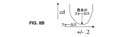
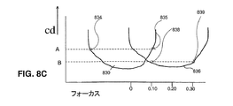
OPCシフトされた(デフォーカスされた)ペアラインショートニングアレイ800の例は図8Aに示される。デフォーカスされたアレイ800は、レチクル上に見えるのと同じにように見える。前述のようなOPC技術は、レチクル上のテスト構造に応用され、それによりテスト構造、すなわちデュアルトーンラインショートニングアレイがウェーハ上に、フォーカスがはずれて露光がなされたのと全く同じように転写される。形状802、803は、例えば、延長フィーチャ808と共に構成されえ、それにより形状803のようなテスト構造主要フィーチャは、プロセス変化により多くのプルバックを示し(すなわちより高い感度を示し)、さらにデフォーカス状態で転写する。スペース804、805は、主要テスト構造フィーチャ802がプロセス変化に対して感度がより低くなるようにさせるために減感スキャッタバー806と共に構成されえる。図8Bに示されるように、光学的に測定された微小寸法のグラフは、デフォーカスされたテスト構造について+または−0.2ミクロンにおいて中心付けられた応答を示す(OPCフィーチャが対称的に適用されてアレイのそれぞれの部分が均等な感度を持つテスト構造に対して)。この実施形態において、OPC技術はテスト構造に適用され、それによりテスト構造の転写がフォーカスがずれて行われるようにする。この技術は、最良フォーカスにおいて転写された1つ以上のテスト構造と同じ露光フィールドにおいてテスト構造が最良フォーカスにおいて転写されることを可能にする。この技術は、それらを意図的にフォーカスをずらして転写することによってテスト構造を追加露光フィールドに転写する、従来技術において記載された歩留まりの損失を招く技術を避ける。フォーカスシフトの向きは、標準(最良フォーカスにおける)ターゲット構造から決定される光学微小寸法を、1つ以上のデフォーカスされたターゲット構造の光学微小寸法と共に評価することによって決定されえる。例えば図8Cは、最良フォーカスにおいて転写されたテスト構造およびデフォーカスされた状態(+0.2ミクロン)で転写されたテスト構造を用いたフォーカスシフトの向きの決定の例を示す。標準ターゲット構造についてのフォーカス応答曲線830は、最良フォーカス位置(0ミクロン)に近傍に中心付けられて示される。AのCD測定例は、プロセスがフォーカスにおいて、点834および835に対応する+または−0.10ミクロンのデフォーカスされた状態にシフトしたことを示唆する。デフォーカスされたテスト構造についてのフォーカス応答曲線836は、+0.2ミクロンにおいて中心付けられて示される。同じプロセス条件についてのBにおけるCD測定例は、それぞれ点838および839に対応する0.10または0.30ミクロンのいずれかだけプロセスがシフトしたことを示唆する。よって2つのグラフは、フォーカスのシフトが正の向きであることを示し、フォーカスシフトの向きおよび大きさの両方が決定されることが可能になる。上述のように、プロセスウィンドウのシフトは、較正フェーズにおけるフォーカス露光マトリクスからのターゲット構造微小寸法測定値および相関する値を用いて数学的モデリングによって決定されえる。
An example of an OPC shifted (defocused) pair
これらの非常に非対称なデュアルトーンラインショートニングアレイは、ターゲットパターンを変更するためにOPC補正を用いて作られる。その結果、デュアルトーンアレイは、従来のデュアルトーンラインショートニングアレイに対してシフトされた効果的な最良フォーカス位置を持つ。ターゲット構造と共に用いられるOPCフィーチャを参照して上述された技術によれば、デフォーカスされたアレイからのCD測定値(非対称OPCフィーチャを用いて作られた)は、標準ターゲット構造からのCD測定値(すなわち最良フォーカスにおける)と共に用いられ、フォーカスのドリフトを決定されえる。スキャッタバー805および延長フィーチャ808のようなOPCフィーチャは、アレイ800の主要テストパターンフィーチャ802、803、804、および805に近接して配置されるとき、プロセスウィンドウ変化に対する異なる感度、およびウェーハ上に転写されるとき非対称応答を作りだす。よってOPCフィーチャは、転写されたウェーハ上に現れる転写されたテスト構造がデフォーカスされた状態にあるように設計されえる。望ましいデフォーカス量は実験的に決定されえる。適切な結果は、0.10から0.20ミクロンの範囲のデフォーカスで得られた。テスト構造の光学応答はそれから、上述のようにフォーカスシフトの向きを決定するために用いられえる。結果として生じるOPC補正された非対称テスト構造は、フォーカスがずれて転写された様相をなす。バイナリOPC変化をテスト構造上で非対称に使用することは、デフォーカスされて転写されたテスト構造を低コストで生成し、テスト構造のために複数の露光が行われるとき無駄になる露光フィールド(群)を防ぐ。
These highly asymmetric dual tone line shortening arrays are made using OPC correction to change the target pattern. As a result, the dual tone array has an effective best focus position that is shifted relative to a conventional dual tone line shortening array. According to the technique described above with reference to the OPC features used with the target structure, the CD measurements from the defocused array (made using the asymmetric OPC features) are the CD measurements from the standard target structure. (Ie at best focus) can be used to determine focus drift. OPC features, such as
本発明は、任意の適切な検査システムと共に用いられえる。図9は、本発明のある実施形態において実現されるウェーハを測定するウェーハまたはレチクル検査システム900を示す。自動的にウェーハを搬送するオートローダ908は、ウェーハ検査ステーション950の検査ポート902へ伸びるアーム910を持つロボット912を含む。アーム910は、回転し、参照番号910’で示される状態のときは外部ポート904へ伸びえる。同様に参照番号910’’で示される状態のときは、ロボットアームはウェーハストッカステーション916のストレージポート906に向かって伸びえ、このストッカステーション916は典型的にはウェーハを格納するいくつかのスロットまたはトラックを含む。ロボットアームは、さらに伸びてウェーハ914をウェーハストッカステーション916から取り出すように設計される。
The present invention can be used with any suitable inspection system. FIG. 9 illustrates a wafer or
本発明のある実施形態による典型的な検査プロセスは、例えば後続の検査アプリケーションにおいて用いられるまでウェーハをウェーハストッカステーション916内に格納することを前提で、ウェーハまたはレチクル914が外部ポート904上に置かれた後に始まりえる。ロボットアームはその位置910’においてウェーハを外部ポート904から搬送し、図9に示されるように伸びることによってそれをウェーハストッカステーション916のローディングポート内に格納する。例えばウェーハが必要とされるとき、ロボットアーム910’’はウェーハ914をローディングポートから取り出し、それをウェーハ検査ステーションの検査ポート902上に置く。
A typical inspection process according to an embodiment of the invention places a wafer or
ウェーハ検査ステーション950は、コンピュータシステム952と結合され、ここでは光学測定値がテスト構造から得られた測定値およびレファレンスウェーハ上の露光されたフィールドからのパターンと比較して評価される。ウェーハまたはレチクル検査システムは、欠陥を検出するのにも用いられえる。コンピュータシステム952は、ウェーハ検査ステーション950と統合されてもよく、検査ステーション950と別個であってもよい。ウェーハ検査ステーション950は、設計データ954を形状のリストの形で受け取り、例えば、欠陥を検出する。さらにコンピュータシステム952は、画像データ(すなわちテスト画像)を検出ステーション950から受け取る。画像データは、それをベースライン画像と比較することによって分析され、ベースライン画像は設計データ954から、またはウェーハ914から生成されえる。ウェーハ検査が完了した後、ウェーハ914は外部ポート904上に置かれる。リソグラフィモニタリングおよび制御のために、ウェーハ上のテスト構造から、および検査ステーション950から得られた光学測定値が、図5を参照して用いられ説明されたようなテストウェーハのさまざまな露光フィールドで得られたテスト構造およびパターンの測定値と共に比較されえる。テストウェーハデータは、コンピュータシステム952によって格納され評価されえる。
本発明の方法を実現し制御(さまざまなスキャニング装置要素の設定を制御すること、ウェーハのベースライン画像を格納および取り出しを行うこと、ウェーハのテスト画像を格納すること、テスト画像を1つ以上のベースライン画像と比較すること、ラインショートニング測定値およびそのような比較中の統計的情報を格納することなど)するのに用いられる適切なコンピュータシステムは、さまざまなベンダー(例えばカリフォルニア州、マウンテンビューのシリコングラフィックスまたはカリフォルニア州、サニーベールのサンマイクロシステムズ)から入手されえ、またはKLAーTencorのようなウェーハ検査システムベンダーによってカスタムメードで作られえる。 Implement and control the method of the present invention (controlling the settings of various scanning device elements, storing and retrieving a baseline image of a wafer, storing a test image of a wafer, storing one or more test images Suitable computer systems used to compare with baseline images, store line shortening measurements and statistical information during such comparisons, etc. are available from various vendors (eg, Mountain View, Calif.). (Silicon Graphics or Sun Microsystems, Sunnyvale, Calif.) Or custom made by a wafer inspection system vendor such as KLA-Tencor.
ここで使用される「電子的表現」という語は、任意の機械読み取り可能な表現を含む。典型的にはこのような表現は、磁気、電子、または光学的に読み取り可能な媒体上に記憶される。このような表現の内容は、電気信号、磁気信号、電磁気信号、光学的信号などとして伝送されえる。 As used herein, the term “electronic representation” includes any machine-readable representation. Typically, such representations are stored on magnetic, electronic, or optically readable media. The contents of such expressions can be transmitted as electrical signals, magnetic signals, electromagnetic signals, optical signals, and the like.
好ましくは、光学的または他の検査システムは、本発明の方法ステップの多くを実現するコンピュータシステムと統合される。このような統合システムは好ましくは、少なくとも(a)メモリに記憶されたベースライン画像(好ましくは圧縮された)、(b)ウェーハの光学画像を生成するよう構成された画像化システム、および(c)ベースラインおよび現在のテスト画像を比較することによって、ここで説明された数学的モデルにしたがって、光学測定値に対応するフォーカスおよび露光量応答を計算し、さまざまな統計情報を格納すると共に、欠陥を特定するよう構成された処理ユニットを含む。少なくとも、画像化システムは、ふつう(i)照射をウェーハの特定位置に導く照射源、および(ii)ウェーハによって散乱されたソースからのウェーハの画像を検出するよう方向付けられた1つ以上の検出器を含む。画像化システムはまたスキャニング手段を含みえる。 Preferably, an optical or other inspection system is integrated with a computer system that implements many of the method steps of the present invention. Such an integrated system preferably includes at least (a) a baseline image (preferably compressed) stored in memory, (b) an imaging system configured to generate an optical image of the wafer, and (c) ) By comparing the baseline and the current test image, according to the mathematical model described here, calculate the focus and exposure response corresponding to the optical measurements, store various statistical information and Including a processing unit configured to identify At least the imaging system typically includes (i) an illumination source that directs illumination to a specific location on the wafer, and (ii) one or more detections directed to detect an image of the wafer from a source scattered by the wafer. Including a bowl. The imaging system can also include scanning means.
前述の本発明は、明瞭な理解の目的のためにある程度詳細に説明されてきたが、ある種の改変および変更が添付の特許請求の範囲内で実施されえることは明らかだろう。本発明の方法および装置を実現する多くの代替的な方法が存在ことに注意されたい。例えば、サブ解像度フィーチャは、ウェーハ上へのラインまたはパターンの転写に光学近接補正効果を作る任意のフィーチャでありえる。さらに本発明は、微小寸法が準拠していること、および微小寸法の測定値を求めるために薄くフィニッシュされた(thin finished)ウェーハを検査するのに特に有用でありえる。したがって本実施形態は、例示的であって限定的ではなく、本発明はここに与えられた詳細に限定されることはなく、添付の特許請求の範囲および等価物の中で改変されえる。 Although the foregoing invention has been described in some detail for purposes of clarity of understanding, it will be apparent that certain modifications and changes may be practiced within the scope of the appended claims. It should be noted that there are many alternative ways of implementing the method and apparatus of the present invention. For example, a sub-resolution feature can be any feature that creates an optical proximity correction effect in the transfer of a line or pattern onto the wafer. In addition, the present invention can be particularly useful for inspecting thin finished wafers to determine that micro dimensions are compliant and to measure micro dimensions. Accordingly, the embodiments are illustrative and not restrictive, and the invention is not limited to the details provided herein, but can be modified within the scope of the appended claims and equivalents.
Claims (22)
テスト構造の転写特性を変更するための波面エンジニアリングフィーチャを有するテスト構造をレチクル上に形成することであって、それぞれ互いに異なる前記波面エンジニアリングフィーチャを有する第1のテスト構造および第2のテスト構造を前記レチクル上に形成することと、
ウェーハテスト構造を形成するための同一の前記リソグラフィプロセスを用いて前記第1のテスト構造および前記第2のテスト構造を第1のウェーハに転写することであって、前記第1のテスト構造をフォーカスが合った状態で転写するとともに前記第2のテスト構造をフォーカスがずれた状態で転写することを含む転写すること、および
前記ウェーハテスト構造の少なくとも一部を測定し、参照寸法と比較することによって、少なくとも1つのリソグラフィプロセスパラメータが変化したかを決定すると共に、前記少なくとも1つのリソグラフィプロセスパラメータの変化の間接的測定を提供すること、
前記第1のウェーハに転写された前記第1のテスト構造および前記第2のテスト構造を測定し、測定結果と前記第1のテスト構造のフォーカス応答曲線および前記第2のテスト構造のフォーカス応答曲線とに基づき、少なくとも1つのリソグラフィプロセスパラメータの変化の方向を決定することと、
前記リソグラフィプロセスが変化したときに、前記少なくとも1つのリソグラフィプロセスパラメータを調整すること
を含む方法。A method for controlling semiconductor lithography process parameters comprising:
Forming a test structure having a wavefront engineering feature on a reticle for changing a transfer characteristic of the test structure, the first test structure and the second test structure having the wavefront engineering features different from each other, Forming on a reticle;
Said first test structure and the second test structure using the same of the lithographic process for forming a wafer test structure be to transfer the first wafer, said first test structure transcribing comprises transferring a state where focusing said second test structure is shifted with transfer in a state where focus suits, and measuring at least a portion of the wafer test structure, compared to a reference dimension Determining whether the at least one lithography process parameter has changed, and providing an indirect measurement of the change in the at least one lithography process parameter ;
Focus response of the first wafer the transferred first test structure and the second test structure was measured, the focus response curve and the second test structure of the the measurement results first test structure Determining a direction of change of at least one lithography process parameter based on the curve ;
Adjusting the at least one lithography process parameter when the lithography process changes.
前記参照寸法は、前記第1のウェーハと第2のウェーハとの一方上に形成される前記ウェーハテスト構造の少なくとも一部の測定により得られる、方法。The method of claim 1, comprising:
The method wherein the reference dimension is obtained by measuring at least a portion of the wafer test structure formed on one of the first and second wafers.
第1のテスト構造および第2のテスト構造を持つパターンをレチクル上に形成すること、および
前記第1のテスト構造および前記第2のテスト構造のそれぞれに近接して互いに異なる波面エンジニアリングフィーチャを配置することによって、リソグラフィプロセスにおいて前記第1のテスト構造および前記第2のテスト構造の転写を制御すること
を含み、
前記第1のテスト構造および前記第2のテスト構造は、デュアルトーンラインショートニングアレイを備え、
前記波面エンジニアリングフィーチャは、前記パターンが複数のウェーハ上に転写されるとき、前記パターンのうちの前記第1のテスト構造部分および前記第2のテスト構造部分がプロセス変化に対して予め選択された感度であるように構成され、
前記方法は、さらに、
前記パターンの前記第1のテスト構造部分がフォーカスが合い前記第2のテスト構造部分がフォーカスがずれた状態でウェーハ上に前記パターンを形成すること、
前記ウェーハ上に形成された前記パターンの前記アレイ部分を測定することによって、ウェーハ上の前記パターンの他の形成に比較して前記プロセスが変化したかを決定すること、
前記ウェーハ上に形成された前記パターンの前記第1のテスト構造部分および前記第2のテスト構造部分を測定し、測定結果と前記第1のテスト構造のフォーカス応答曲線および前記第2のテスト構造のフォーカス応答曲線とに基づき、少なくとも1つのプロセスパラメータの変化の方向を決定すること、および
前記プロセスパラメータをそれらが変化したときに調整すること、を含む
方法。A method for controlling semiconductor process parameters comprising:
Forming a pattern having a first test structure and a second test structure on a reticle; and disposing different wavefront engineering features in proximity to each of the first test structure and the second test structure. By controlling the transfer of the first test structure and the second test structure in a lithography process,
The first test structure and the second test structure comprise a dual tone line shortening array;
The wavefront engineering feature is characterized in that when the pattern is transferred onto a plurality of wafers, the first test structure portion and the second test structure portion of the pattern are preselected for process changes. Is configured to be
The method further comprises:
A child form the pattern on the wafer in a state in which the second test structure portion first test structure portion fit focus of the pattern is shifted focus,
By measuring the array portion of the pattern formed on the wafer, that compared to other formation of the pattern on the wafer to determine whether the process has changed,
The first test structure portion and the second test structure portion of the pattern formed on the wafer are measured , the measurement result, the focus response curve of the first test structure, and the second test structure of the second test structure are measured. Determining a direction of change of at least one process parameter based on the focus response curve and adjusting the process parameter as they change.
第1のテスト構造および第2のテスト構造を持つパターンをレチクル上に形成すること、および
ウェーハ上に転写された前記パターンのラインエンドショートニングを位相シフト技術を用いて制御することによって前記パターンのウェーハ上への転写を制御すること
を含み、
前記位相シフト技術は、前記パターンが複数のウェーハ上に転写されるとき、前記パターンがプロセス変化に対して感度を持つように選択され、
前記方法は、さらに、
前記パターンの前記第1のテスト構造部分がフォーカスが合い前記第2のテスト構造部分がフォーカスがずれた状態でウェーハ上に前記パターンを形成すること、
前記ウェーハ上の前記形成されたパターンを測定することによって、ウェーハ上の前記パターンの他の形成に比較して前記プロセスが変化したかを決定すること、
前記ウェーハ上に形成された前記パターンの前記第1のテスト構造部分および前記第2のテスト構造部分を測定し、測定結果と前記第1のテスト構造のフォーカス応答曲線および前記第2のテスト構造のフォーカス応答曲線とに基づき、少なくとも1つのプロセスパラメータの変化の方向を決定すること、および
前記プロセスパラメータをそれらが変化したときに調整すること、を含む
方法。A method for controlling semiconductor process parameters comprising:
Forming a pattern having a first test structure and a second test structure on a reticle, and controlling the line end shortening of the pattern transferred onto the wafer using a phase shift technique; Including controlling transcription on the top,
The phase shift technique is selected such that when the pattern is transferred onto a plurality of wafers, the pattern is sensitive to process changes;
The method further comprises:
A child form the pattern on the wafer in a state in which the second test structure portion first test structure portion fit focus of the pattern is shifted focus,
By measuring the pattern formed on the wafer, that compared to other formation of the pattern on the wafer to determine whether the process has changed,
The first test structure portion and the second test structure portion of the pattern formed on the wafer are measured , the measurement result, the focus response curve of the first test structure, and the second test structure of the second test structure are measured. Determining a direction of change of at least one process parameter based on the focus response curve and adjusting the process parameter as they change.
前記測定した部分が前記参照寸法を所定の閾値分超える場合に、前記リソグラフィプロセスパラメータを調整することをさらに含む、方法。The method of claim 1, comprising:
Adjusting the lithography process parameters if the measured portion exceeds the reference dimension by a predetermined threshold.
前記波面エンジニアリングフィーチャは、前記少なくとも1つのリソグラフィプロセスパラメータが所定の閾値分変化するとき、前記ウェーハテスト構造に所定の変化を引き起こすように構成されている、方法。The method of claim 1, comprising:
The wavefront engineering feature is configured to cause a predetermined change in the wafer test structure when the at least one lithography process parameter changes by a predetermined threshold.
Applications Claiming Priority (5)
| Application Number | Priority Date | Filing Date | Title |
|---|---|---|---|
| US33571201P | 2001-11-14 | 2001-11-14 | |
| US60/335,712 | 2001-11-14 | ||
| US10/058,572 | 2002-01-28 | ||
| US10/058,572 US6673638B1 (en) | 2001-11-14 | 2002-01-28 | Method and apparatus for the production of process sensitive lithographic features |
| PCT/US2002/036819 WO2003043075A1 (en) | 2001-11-14 | 2002-11-14 | Method and apparatus for the production of process sensitive lithographic features |
Publications (3)
| Publication Number | Publication Date |
|---|---|
| JP2005510058A JP2005510058A (en) | 2005-04-14 |
| JP2005510058A5 JP2005510058A5 (en) | 2006-02-16 |
| JP5013657B2 true JP5013657B2 (en) | 2012-08-29 |
Family
ID=26737761
Family Applications (1)
| Application Number | Title | Priority Date | Filing Date |
|---|---|---|---|
| JP2003544809A Expired - Fee Related JP5013657B2 (en) | 2001-11-14 | 2002-11-14 | Method for controlling semiconductor process parameters |
Country Status (3)
| Country | Link |
|---|---|
| US (1) | US6673638B1 (en) |
| JP (1) | JP5013657B2 (en) |
| WO (1) | WO2003043075A1 (en) |
Families Citing this family (88)
| Publication number | Priority date | Publication date | Assignee | Title |
|---|---|---|---|---|
| JP2003142376A (en) * | 2001-11-02 | 2003-05-16 | Canon Inc | Lithographic system, aligner, method of controlling them, and method of manufacturing device |
| KR100434110B1 (en) * | 2002-06-04 | 2004-06-04 | 삼성전자주식회사 | Method of Manufacturing Semiconductor Device |
| US6711732B1 (en) * | 2002-07-26 | 2004-03-23 | Taiwan Semiconductor Manufacturing Company | Full sized scattering bar alt-PSM technique for IC manufacturing in sub-resolution era |
| JP4302965B2 (en) * | 2002-11-01 | 2009-07-29 | 株式会社日立ハイテクノロジーズ | Semiconductor device manufacturing method and manufacturing system thereof |
| US6746882B1 (en) * | 2002-11-21 | 2004-06-08 | Advanced Micro Devices, Inc. | Method of correcting non-linearity of metrology tools, and system for performing same |
| US7042550B2 (en) * | 2002-11-28 | 2006-05-09 | Asml Netherlands B.V. | Device manufacturing method and computer program |
| US7352453B2 (en) * | 2003-01-17 | 2008-04-01 | Kla-Tencor Technologies Corporation | Method for process optimization and control by comparison between 2 or more measured scatterometry signals |
| US7778721B2 (en) * | 2003-01-27 | 2010-08-17 | Applied Materials, Inc. | Small lot size lithography bays |
| US7221993B2 (en) * | 2003-01-27 | 2007-05-22 | Applied Materials, Inc. | Systems and methods for transferring small lot size substrate carriers between processing tools |
| WO2004099874A1 (en) * | 2003-04-16 | 2004-11-18 | Nikon Corporation | Pattern decision method and system, mask manufacturing method, focusing performance adjusting method, exposure method and device, program, and information recording medium |
| US6968253B2 (en) * | 2003-05-07 | 2005-11-22 | Kla-Tencor Technologies Corp. | Computer-implemented method and carrier medium configured to generate a set of process parameters for a lithography process |
| CN1902501B (en) * | 2003-07-17 | 2010-06-09 | 凸版光掩膜公司 | Method and apparatus for calibrating a metrology tool |
| US7218983B2 (en) | 2003-11-06 | 2007-05-15 | Applied Materials, Inc. | Method and apparatus for integrating large and small lot electronic device fabrication facilities |
| US7720557B2 (en) * | 2003-11-06 | 2010-05-18 | Applied Materials, Inc. | Methods and apparatus for enhanced operation of substrate carrier handlers |
| JP2005202102A (en) * | 2004-01-15 | 2005-07-28 | Fujitsu Ltd | Mask for exposure, pattern correction method therefor, and method for manufacturing semiconductor device |
| US7274971B2 (en) | 2004-02-28 | 2007-09-25 | Applied Materials, Inc. | Methods and apparatus for electronic device manufacturing system monitoring and control |
| US7177716B2 (en) | 2004-02-28 | 2007-02-13 | Applied Materials, Inc. | Methods and apparatus for material control system interface |
| US7413069B2 (en) * | 2004-02-28 | 2008-08-19 | Applied Materials, Inc. | Methods and apparatus for transferring a substrate carrier within an electronic device manufacturing facility |
| US7146599B2 (en) * | 2004-04-15 | 2006-12-05 | Taiwan Semiconductor Manufacturing Co., Ltd. | Method for using asymmetric OPC structures on line ends of semiconductor pattern layers |
| TWI333233B (en) * | 2004-06-10 | 2010-11-11 | Applied Materials Inc | Small lot size lithography bays |
| US7369697B2 (en) * | 2004-06-17 | 2008-05-06 | Intel Corporation | Process variable of interest monitoring and control |
| US7052921B1 (en) * | 2004-09-03 | 2006-05-30 | Advanced Micro Devices, Inc. | System and method using in situ scatterometry to detect photoresist pattern integrity during the photolithography process |
| US7251807B2 (en) * | 2005-02-24 | 2007-07-31 | Synopsys, Inc. | Method and apparatus for identifying a manufacturing problem area in a layout using a process-sensitivity model |
| US7814456B2 (en) * | 2004-11-22 | 2010-10-12 | Tela Innovations, Inc. | Method and system for topography-aware reticle enhancement |
| JP4389222B2 (en) * | 2005-05-02 | 2009-12-24 | エルピーダメモリ株式会社 | How to create mask data |
| US7519940B2 (en) * | 2005-05-02 | 2009-04-14 | Cadence Design Systems, Inc. | Apparatus and method for compensating a lithography projection tool |
| US7536670B2 (en) * | 2005-05-31 | 2009-05-19 | Cadence Design Systems, Inc. | Method for verifying and choosing lithography model |
| US7392502B2 (en) * | 2005-06-30 | 2008-06-24 | Invarium, Inc. | Method for real time monitoring and verifying optical proximity correction model and method |
| US7695876B2 (en) * | 2005-08-31 | 2010-04-13 | Brion Technologies, Inc. | Method for identifying and using process window signature patterns for lithography process control |
| US7502702B1 (en) * | 2005-09-07 | 2009-03-10 | Advanced Micro Devices, Inc. | Method and apparatus for dynamic adjustment of sensor and/or metrology sensitivities |
| US7176675B1 (en) * | 2005-11-29 | 2007-02-13 | International Business Machines Corporation | Proximity sensitive defect monitor |
| US7506285B2 (en) | 2006-02-17 | 2009-03-17 | Mohamed Al-Imam | Multi-dimensional analysis for predicting RET model accuracy |
| US8541879B2 (en) | 2007-12-13 | 2013-09-24 | Tela Innovations, Inc. | Super-self-aligned contacts and method for making the same |
| US8658542B2 (en) | 2006-03-09 | 2014-02-25 | Tela Innovations, Inc. | Coarse grid design methods and structures |
| US8653857B2 (en) | 2006-03-09 | 2014-02-18 | Tela Innovations, Inc. | Circuitry and layouts for XOR and XNOR logic |
| US9035359B2 (en) | 2006-03-09 | 2015-05-19 | Tela Innovations, Inc. | Semiconductor chip including region including linear-shaped conductive structures forming gate electrodes and having electrical connection areas arranged relative to inner region between transistors of different types and associated methods |
| US9230910B2 (en) | 2006-03-09 | 2016-01-05 | Tela Innovations, Inc. | Oversized contacts and vias in layout defined by linearly constrained topology |
| US8225261B2 (en) * | 2006-03-09 | 2012-07-17 | Tela Innovations, Inc. | Methods for defining contact grid in dynamic array architecture |
| US8448102B2 (en) * | 2006-03-09 | 2013-05-21 | Tela Innovations, Inc. | Optimizing layout of irregular structures in regular layout context |
| US9563733B2 (en) * | 2009-05-06 | 2017-02-07 | Tela Innovations, Inc. | Cell circuit and layout with linear finfet structures |
| US7932545B2 (en) | 2006-03-09 | 2011-04-26 | Tela Innovations, Inc. | Semiconductor device and associated layouts including gate electrode level region having arrangement of six linear conductive segments with side-to-side spacing less than 360 nanometers |
| US8225239B2 (en) * | 2006-03-09 | 2012-07-17 | Tela Innovations, Inc. | Methods for defining and utilizing sub-resolution features in linear topology |
| US8839175B2 (en) | 2006-03-09 | 2014-09-16 | Tela Innovations, Inc. | Scalable meta-data objects |
| US7446352B2 (en) * | 2006-03-09 | 2008-11-04 | Tela Innovations, Inc. | Dynamic array architecture |
| US7908578B2 (en) * | 2007-08-02 | 2011-03-15 | Tela Innovations, Inc. | Methods for designing semiconductor device with dynamic array section |
| US7763534B2 (en) | 2007-10-26 | 2010-07-27 | Tela Innovations, Inc. | Methods, structures and designs for self-aligning local interconnects used in integrated circuits |
| US9009641B2 (en) | 2006-03-09 | 2015-04-14 | Tela Innovations, Inc. | Circuits with linear finfet structures |
| US7956421B2 (en) * | 2008-03-13 | 2011-06-07 | Tela Innovations, Inc. | Cross-coupled transistor layouts in restricted gate level layout architecture |
| US7943967B2 (en) * | 2006-03-09 | 2011-05-17 | Tela Innovations, Inc. | Semiconductor device and associated layouts including diffusion contact placement restriction based on relation to linear conductive segments |
| US8245180B2 (en) * | 2006-03-09 | 2012-08-14 | Tela Innovations, Inc. | Methods for defining and using co-optimized nanopatterns for integrated circuit design and apparatus implementing same |
| US8247846B2 (en) * | 2006-03-09 | 2012-08-21 | Tela Innovations, Inc. | Oversized contacts and vias in semiconductor chip defined by linearly constrained topology |
| US7925486B2 (en) | 2006-03-14 | 2011-04-12 | Kla-Tencor Technologies Corp. | Computer-implemented methods, carrier media, and systems for creating a metrology target structure design for a reticle layout |
| US7743357B2 (en) * | 2006-05-31 | 2010-06-22 | Synopsys, Inc. | Method and apparatus for determining a process model that models the impact of CAR/PEB on the resist profile |
| US7979829B2 (en) | 2007-02-20 | 2011-07-12 | Tela Innovations, Inc. | Integrated circuit cell library with cell-level process compensation technique (PCT) application and associated methods |
| US8286107B2 (en) * | 2007-02-20 | 2012-10-09 | Tela Innovations, Inc. | Methods and systems for process compensation technique acceleration |
| US8667443B2 (en) | 2007-03-05 | 2014-03-04 | Tela Innovations, Inc. | Integrated circuit cell library for multiple patterning |
| US7687206B2 (en) * | 2007-03-08 | 2010-03-30 | United Microelectronics Corp. | Mask pattern and method for forming the same |
| US20080241708A1 (en) * | 2007-04-02 | 2008-10-02 | Taiwan Semiconductor Manufacturing Company, Ltd. | Sub-resolution assist feature of a photomask |
| US7873504B1 (en) | 2007-05-07 | 2011-01-18 | Kla-Tencor Technologies Corp. | Computer-implemented methods, carrier media, and systems for creating a metrology target structure design for a reticle layout |
| US8453094B2 (en) | 2008-01-31 | 2013-05-28 | Tela Innovations, Inc. | Enforcement of semiconductor structure regularity for localized transistors and interconnect |
| US7939443B2 (en) | 2008-03-27 | 2011-05-10 | Tela Innovations, Inc. | Methods for multi-wire routing and apparatus implementing same |
| KR101739709B1 (en) | 2008-07-16 | 2017-05-24 | 텔라 이노베이션스, 인코포레이티드 | Methods for cell phasing and placement in dynamic array architecture and implementation of the same |
| US9122832B2 (en) * | 2008-08-01 | 2015-09-01 | Tela Innovations, Inc. | Methods for controlling microloading variation in semiconductor wafer layout and fabrication |
| US8214771B2 (en) | 2009-01-08 | 2012-07-03 | Kla-Tencor Corporation | Scatterometry metrology target design optimization |
| US8661392B2 (en) | 2009-10-13 | 2014-02-25 | Tela Innovations, Inc. | Methods for cell boundary encroachment and layouts implementing the Same |
| US8453076B2 (en) * | 2010-03-16 | 2013-05-28 | International Business Machines Corporation | Wavefront engineering of mask data for semiconductor device design |
| US9159627B2 (en) | 2010-11-12 | 2015-10-13 | Tela Innovations, Inc. | Methods for linewidth modification and apparatus implementing the same |
| WO2012097833A1 (en) | 2011-01-20 | 2012-07-26 | Carl Zeiss Smt Gmbh | Method of operating a projection exposure tool |
| US10769320B2 (en) | 2012-12-18 | 2020-09-08 | Kla-Tencor Corporation | Integrated use of model-based metrology and a process model |
| US10274839B2 (en) * | 2013-03-11 | 2019-04-30 | Taiwan Semiconductor Manufacturing Company, Ltd. | Two-dimensional marks |
| US9448343B2 (en) | 2013-03-15 | 2016-09-20 | Kla-Tencor Corporation | Segmented mirror apparatus for imaging and method of using the same |
| US10101670B2 (en) | 2013-03-27 | 2018-10-16 | Kla-Tencor Corporation | Statistical model-based metrology |
| US9875946B2 (en) | 2013-04-19 | 2018-01-23 | Kla-Tencor Corporation | On-device metrology |
| US9383661B2 (en) | 2013-08-10 | 2016-07-05 | Kla-Tencor Corporation | Methods and apparatus for determining focus |
| US10935893B2 (en) | 2013-08-11 | 2021-03-02 | Kla-Tencor Corporation | Differential methods and apparatus for metrology of semiconductor targets |
| US9490182B2 (en) | 2013-12-23 | 2016-11-08 | Kla-Tencor Corporation | Measurement of multiple patterning parameters |
| WO2016083076A1 (en) | 2014-11-26 | 2016-06-02 | Asml Netherlands B.V. | Metrology method, computer product and system |
| KR102323388B1 (en) | 2015-05-15 | 2021-11-05 | 케이엘에이 코포레이션 | Systems and methods for focus determination using focus-sensitive overlay targets |
| US10216096B2 (en) | 2015-08-14 | 2019-02-26 | Kla-Tencor Corporation | Process-sensitive metrology systems and methods |
| JP2017053674A (en) | 2015-09-08 | 2017-03-16 | 株式会社ニューフレアテクノロジー | Displacement amount measurement method of pattern width dimension and pattern inspection device |
| US20170256465A1 (en) | 2016-03-01 | 2017-09-07 | Asml Netherlands B.V. | Method and apparatus to determine a patterning process parameter |
| US9711420B1 (en) * | 2016-03-14 | 2017-07-18 | Taiwan Semiconductor Manufacturing Co., Ltd. | Inline focus monitoring |
| KR102450492B1 (en) * | 2016-10-21 | 2022-09-30 | 에이에스엠엘 네델란즈 비.브이. | Methods of determining corrections for a patterning process |
| US10209627B2 (en) | 2017-01-06 | 2019-02-19 | Kla-Tencor Corporation | Systems and methods for focus-sensitive metrology targets |
| US10133838B2 (en) * | 2017-01-30 | 2018-11-20 | Dongfang Jingyuan Electron Limited | Guided defect detection of integrated circuits |
| EP3396456A1 (en) * | 2017-04-25 | 2018-10-31 | ASML Netherlands B.V. | Method of monitoring and device manufacturing method |
| CN108957943B (en) | 2017-05-22 | 2021-02-19 | 联华电子股份有限公司 | Method for forming layout pattern |
| WO2020141040A1 (en) * | 2019-01-03 | 2020-07-09 | Asml Netherlands B.V. | Methods and patterning devices and apparatuses for measuring focus performance of a lithographic apparatus, device manufacturing method |
Family Cites Families (23)
| Publication number | Priority date | Publication date | Assignee | Title |
|---|---|---|---|---|
| US4855253A (en) * | 1988-01-29 | 1989-08-08 | Hewlett-Packard | Test method for random defects in electronic microstructures |
| US5103557A (en) * | 1988-05-16 | 1992-04-14 | Leedy Glenn J | Making and testing an integrated circuit using high density probe points |
| US5682323A (en) * | 1995-03-06 | 1997-10-28 | Lsi Logic Corporation | System and method for performing optical proximity correction on macrocell libraries |
| JP2917879B2 (en) * | 1995-10-31 | 1999-07-12 | 日本電気株式会社 | Photomask and manufacturing method thereof |
| JP4180678B2 (en) * | 1997-05-29 | 2008-11-12 | 株式会社東芝 | Exposure method |
| JP3067695B2 (en) * | 1997-06-06 | 2000-07-17 | 日本電気株式会社 | Inspection method for projection exposure apparatus |
| US5976740A (en) | 1997-08-28 | 1999-11-02 | International Business Machines Corporation | Process for controlling exposure dose or focus parameters using tone reversing pattern |
| US5970311A (en) * | 1997-10-31 | 1999-10-19 | Advanced Micro Devices | Method and structure for optimizing the performance of a semiconductor device having dense transistors |
| US6174741B1 (en) * | 1997-12-19 | 2001-01-16 | Siemens Aktiengesellschaft | Method for quantifying proximity effect by measuring device performance |
| JPH11233434A (en) * | 1998-02-17 | 1999-08-27 | Nikon Corp | Exposure condition determining method, exposure method, aligner, and manufacture of device |
| US6174630B1 (en) * | 1998-03-03 | 2001-01-16 | Lsi Logic Corporation | Method of proximity correction with relative segmentation |
| JP2000124103A (en) * | 1998-10-16 | 2000-04-28 | Sony Corp | Exposure method and aligner |
| US6374396B1 (en) * | 1998-12-04 | 2002-04-16 | Micron Technology, Inc. | Correction of field effects in photolithography |
| JP2000181045A (en) * | 1998-12-10 | 2000-06-30 | Matsushita Electronics Industry Corp | Pattern correcting method |
| US6294397B1 (en) * | 1999-03-04 | 2001-09-25 | Advanced Micro Devices, Inc. | Drop-in test structure and abbreviated integrated circuit process flow for characterizing production integrated circuit process flow, topography, and equipment |
| US6345210B1 (en) * | 1999-03-08 | 2002-02-05 | Advanced Micro Devices, Inc. | Method of using critical dimension mapping to qualify a reticle used in integrated circuit fabrication |
| US6120953A (en) * | 1999-04-23 | 2000-09-19 | United Microelectronics Corp. | Method of optical proximity correction |
| US6143579A (en) * | 1999-04-26 | 2000-11-07 | Taiwan Semiconductor Manufacturing Ltd. | Efficient method for monitoring gate oxide damage related to plasma etch chamber processing history |
| US6444373B1 (en) * | 2000-06-16 | 2002-09-03 | Advanced Micro Devices, Inc. | Modification of mask layout data to improve mask fidelity |
| US6448099B1 (en) * | 2000-11-28 | 2002-09-10 | Advanced Micro Devices, Inc. | Method and apparatus for detecting voltage contrast in a semiconductor wafer |
| US6365422B1 (en) * | 2001-01-22 | 2002-04-02 | Advanced Micro Devices, Inc. | Automated variation of stepper exposure dose based upon across wafer variations in device characteristics, and system for accomplishing same |
| US6433878B1 (en) * | 2001-01-29 | 2002-08-13 | Timbre Technology, Inc. | Method and apparatus for the determination of mask rules using scatterometry |
| US6458605B1 (en) * | 2001-06-28 | 2002-10-01 | Advanced Micro Devices, Inc. | Method and apparatus for controlling photolithography overlay registration |
-
2002
- 2002-01-28 US US10/058,572 patent/US6673638B1/en not_active Expired - Lifetime
- 2002-11-14 JP JP2003544809A patent/JP5013657B2/en not_active Expired - Fee Related
- 2002-11-14 WO PCT/US2002/036819 patent/WO2003043075A1/en active Application Filing
Also Published As
| Publication number | Publication date |
|---|---|
| WO2003043075A1 (en) | 2003-05-22 |
| JP2005510058A (en) | 2005-04-14 |
| US6673638B1 (en) | 2004-01-06 |
Similar Documents
| Publication | Publication Date | Title |
|---|---|---|
| JP5013657B2 (en) | Method for controlling semiconductor process parameters | |
| JP4954211B2 (en) | System and method for performing mask verification using an individual mask error model | |
| JP5371179B2 (en) | System and method for measuring focus changes in a photolithography process using test features printed from a test pattern image of a photomask | |
| JP3972035B2 (en) | Inspection method and device manufacturing method | |
| US7327436B2 (en) | Method for evaluating a local flare, correction method for a mask pattern, manufacturing method for a semiconductor device and a computer program product | |
| US7536670B2 (en) | Method for verifying and choosing lithography model | |
| CN1862385B (en) | System and method for detecting focus change in photolithographic process using test characteristic | |
| TW201939174A (en) | Methods for processing metrology data, processing variables of a pattern of a substrate and predicting a contour, and computer program product | |
| JP2002311564A (en) | Method and apparatus for determining mask rule using scatterometry | |
| JP4057847B2 (en) | Lithographic projection apparatus calibration method, patterning apparatus, and device manufacturing method | |
| JP2006301631A (en) | Photomask structure providing improved photolithographic step window and method of manufacturing the same | |
| JP2017538155A (en) | Method and apparatus for using patterning device topography induced phase | |
| TW201633003A (en) | Method and apparatus for using patterning device topography induced phase | |
| KR101175341B1 (en) | Device and method for determining an illumination intensity profile of an illuminator for a lithography system | |
| TWI604277B (en) | Method and apparatus for using patterning device topography induced phase | |
| TWI623822B (en) | Method and computer program for inspecting a substrate | |
| TW201632984A (en) | Method and apparatus for using patterning device topography induced phase | |
| TWI636317B (en) | Method for using patterning device topography induced phase, non-transitory computer program, and method for manufacturing semiconductor devices | |
| TWI769625B (en) | Method for determining a measurement recipe and associated apparatuses | |
| TWI706233B (en) | Method, patterning device, lithographic system and non-transitory computer program product of determining a characteristic of interest relating to a structure on a substrate formed by a lithographic process | |
| JP2009239029A (en) | Method for evaluating lithography apparatus and method for controlling lithography apparatus | |
| JP2004200691A (en) | Method for characterizing lens system, and mask | |
| CN117882011A (en) | Method of monitoring a lithographic process and related apparatus |
Legal Events
| Date | Code | Title | Description |
|---|---|---|---|
| A621 | Written request for application examination |
Free format text: JAPANESE INTERMEDIATE CODE: A621 Effective date: 20051114 |
|
| A521 | Request for written amendment filed |
Free format text: JAPANESE INTERMEDIATE CODE: A523 Effective date: 20051220 |
|
| A131 | Notification of reasons for refusal |
Free format text: JAPANESE INTERMEDIATE CODE: A131 Effective date: 20090407 |
|
| A601 | Written request for extension of time |
Free format text: JAPANESE INTERMEDIATE CODE: A601 Effective date: 20090706 |
|
| A602 | Written permission of extension of time |
Free format text: JAPANESE INTERMEDIATE CODE: A602 Effective date: 20090713 |
|
| A521 | Request for written amendment filed |
Free format text: JAPANESE INTERMEDIATE CODE: A523 Effective date: 20091006 |
|
| A131 | Notification of reasons for refusal |
Free format text: JAPANESE INTERMEDIATE CODE: A131 Effective date: 20100907 |
|
| A601 | Written request for extension of time |
Free format text: JAPANESE INTERMEDIATE CODE: A601 Effective date: 20101203 |
|
| A602 | Written permission of extension of time |
Free format text: JAPANESE INTERMEDIATE CODE: A602 Effective date: 20101210 |
|
| A521 | Request for written amendment filed |
Free format text: JAPANESE INTERMEDIATE CODE: A523 Effective date: 20110303 |
|
| A131 | Notification of reasons for refusal |
Free format text: JAPANESE INTERMEDIATE CODE: A131 Effective date: 20120110 |
|
| A521 | Request for written amendment filed |
Free format text: JAPANESE INTERMEDIATE CODE: A523 Effective date: 20120406 |
|
| TRDD | Decision of grant or rejection written | ||
| A01 | Written decision to grant a patent or to grant a registration (utility model) |
Free format text: JAPANESE INTERMEDIATE CODE: A01 Effective date: 20120508 |
|
| A01 | Written decision to grant a patent or to grant a registration (utility model) |
Free format text: JAPANESE INTERMEDIATE CODE: A01 |
|
| A61 | First payment of annual fees (during grant procedure) |
Free format text: JAPANESE INTERMEDIATE CODE: A61 Effective date: 20120605 |
|
| FPAY | Renewal fee payment (event date is renewal date of database) |
Free format text: PAYMENT UNTIL: 20150615 Year of fee payment: 3 |
|
| R150 | Certificate of patent or registration of utility model |
Free format text: JAPANESE INTERMEDIATE CODE: R150 Ref document number: 5013657 Country of ref document: JP Free format text: JAPANESE INTERMEDIATE CODE: R150 |
|
| R250 | Receipt of annual fees |
Free format text: JAPANESE INTERMEDIATE CODE: R250 |
|
| R250 | Receipt of annual fees |
Free format text: JAPANESE INTERMEDIATE CODE: R250 |
|
| R250 | Receipt of annual fees |
Free format text: JAPANESE INTERMEDIATE CODE: R250 |
|
| R250 | Receipt of annual fees |
Free format text: JAPANESE INTERMEDIATE CODE: R250 |
|
| R250 | Receipt of annual fees |
Free format text: JAPANESE INTERMEDIATE CODE: R250 |
|
| R250 | Receipt of annual fees |
Free format text: JAPANESE INTERMEDIATE CODE: R250 |
|
| R250 | Receipt of annual fees |
Free format text: JAPANESE INTERMEDIATE CODE: R250 |
|
| LAPS | Cancellation because of no payment of annual fees |