JP4982948B2 - Manufacturing method of semiconductor device - Google Patents
Manufacturing method of semiconductor device Download PDFInfo
- Publication number
- JP4982948B2 JP4982948B2 JP2005017486A JP2005017486A JP4982948B2 JP 4982948 B2 JP4982948 B2 JP 4982948B2 JP 2005017486 A JP2005017486 A JP 2005017486A JP 2005017486 A JP2005017486 A JP 2005017486A JP 4982948 B2 JP4982948 B2 JP 4982948B2
- Authority
- JP
- Japan
- Prior art keywords
- conductivity type
- main surface
- groove
- region
- separation layer
- Prior art date
- Legal status (The legal status is an assumption and is not a legal conclusion. Google has not performed a legal analysis and makes no representation as to the accuracy of the status listed.)
- Expired - Fee Related
Links
- 239000004065 semiconductor Substances 0.000 title claims description 143
- 238000004519 manufacturing process Methods 0.000 title claims description 62
- 239000010410 layer Substances 0.000 claims description 147
- 238000000926 separation method Methods 0.000 claims description 80
- 238000000034 method Methods 0.000 claims description 74
- 239000000758 substrate Substances 0.000 claims description 56
- 239000012535 impurity Substances 0.000 claims description 34
- 238000005468 ion implantation Methods 0.000 claims description 32
- 238000000347 anisotropic wet etching Methods 0.000 claims description 24
- 239000012670 alkaline solution Substances 0.000 claims description 18
- 230000015572 biosynthetic process Effects 0.000 claims description 15
- 238000011049 filling Methods 0.000 claims description 14
- 238000010438 heat treatment Methods 0.000 claims description 13
- 230000001681 protective effect Effects 0.000 claims description 6
- 239000002344 surface layer Substances 0.000 claims description 4
- 238000000151 deposition Methods 0.000 claims 1
- 235000012431 wafers Nutrition 0.000 description 79
- 230000002441 reversible effect Effects 0.000 description 60
- 230000000903 blocking effect Effects 0.000 description 57
- 238000005530 etching Methods 0.000 description 57
- 238000009792 diffusion process Methods 0.000 description 55
- 229910052710 silicon Inorganic materials 0.000 description 38
- 239000010703 silicon Substances 0.000 description 38
- XUIMIQQOPSSXEZ-UHFFFAOYSA-N Silicon Chemical compound [Si] XUIMIQQOPSSXEZ-UHFFFAOYSA-N 0.000 description 30
- 230000008569 process Effects 0.000 description 30
- 229910052796 boron Inorganic materials 0.000 description 28
- ZOXJGFHDIHLPTG-UHFFFAOYSA-N Boron Chemical compound [B] ZOXJGFHDIHLPTG-UHFFFAOYSA-N 0.000 description 26
- 230000003647 oxidation Effects 0.000 description 24
- 238000007254 oxidation reaction Methods 0.000 description 24
- 238000005224 laser annealing Methods 0.000 description 21
- 238000000137 annealing Methods 0.000 description 17
- 230000015556 catabolic process Effects 0.000 description 17
- 238000002955 isolation Methods 0.000 description 15
- VYPSYNLAJGMNEJ-UHFFFAOYSA-N silicon dioxide Inorganic materials O=[Si]=O VYPSYNLAJGMNEJ-UHFFFAOYSA-N 0.000 description 15
- KWYUFKZDYYNOTN-UHFFFAOYSA-M Potassium hydroxide Chemical compound [OH-].[K+] KWYUFKZDYYNOTN-UHFFFAOYSA-M 0.000 description 14
- 239000002390 adhesive tape Substances 0.000 description 14
- 239000002585 base Substances 0.000 description 14
- 239000002019 doping agent Substances 0.000 description 14
- 230000000694 effects Effects 0.000 description 13
- 230000002829 reductive effect Effects 0.000 description 12
- QVGXLLKOCUKJST-UHFFFAOYSA-N atomic oxygen Chemical compound [O] QVGXLLKOCUKJST-UHFFFAOYSA-N 0.000 description 11
- 239000001301 oxygen Substances 0.000 description 11
- 229910052760 oxygen Inorganic materials 0.000 description 11
- 239000013078 crystal Substances 0.000 description 10
- 238000001312 dry etching Methods 0.000 description 10
- 238000005520 cutting process Methods 0.000 description 9
- 229910052814 silicon oxide Inorganic materials 0.000 description 9
- 239000006260 foam Substances 0.000 description 8
- 239000000243 solution Substances 0.000 description 8
- WGTYBPLFGIVFAS-UHFFFAOYSA-M tetramethylammonium hydroxide Chemical compound [OH-].C[N+](C)(C)C WGTYBPLFGIVFAS-UHFFFAOYSA-M 0.000 description 8
- 229910052782 aluminium Inorganic materials 0.000 description 7
- 238000012545 processing Methods 0.000 description 7
- 239000000126 substance Substances 0.000 description 7
- 239000012790 adhesive layer Substances 0.000 description 6
- XAGFODPZIPBFFR-UHFFFAOYSA-N aluminium Chemical compound [Al] XAGFODPZIPBFFR-UHFFFAOYSA-N 0.000 description 6
- 239000007864 aqueous solution Substances 0.000 description 6
- 239000011248 coating agent Substances 0.000 description 6
- 238000000576 coating method Methods 0.000 description 6
- 230000007423 decrease Effects 0.000 description 6
- 230000007547 defect Effects 0.000 description 6
- 239000004642 Polyimide Substances 0.000 description 5
- 238000005229 chemical vapour deposition Methods 0.000 description 5
- 238000000227 grinding Methods 0.000 description 5
- 229920001721 polyimide Polymers 0.000 description 5
- 239000010453 quartz Substances 0.000 description 5
- 230000004913 activation Effects 0.000 description 4
- 239000005380 borophosphosilicate glass Substances 0.000 description 4
- 238000002513 implantation Methods 0.000 description 4
- 239000011229 interlayer Substances 0.000 description 4
- 238000002844 melting Methods 0.000 description 4
- 230000008018 melting Effects 0.000 description 4
- 229910052751 metal Inorganic materials 0.000 description 4
- 239000002184 metal Substances 0.000 description 4
- 229910021420 polycrystalline silicon Inorganic materials 0.000 description 4
- 229920005591 polysilicon Polymers 0.000 description 4
- 239000012779 reinforcing material Substances 0.000 description 4
- 238000003892 spreading Methods 0.000 description 4
- 230000007480 spreading Effects 0.000 description 4
- -1 SOG Substances 0.000 description 3
- 229910052581 Si3N4 Inorganic materials 0.000 description 3
- 230000002457 bidirectional effect Effects 0.000 description 3
- 230000007812 deficiency Effects 0.000 description 3
- 230000006866 deterioration Effects 0.000 description 3
- 239000007789 gas Substances 0.000 description 3
- 238000010884 ion-beam technique Methods 0.000 description 3
- 230000036961 partial effect Effects 0.000 description 3
- 229920001709 polysilazane Polymers 0.000 description 3
- 229920001296 polysiloxane Polymers 0.000 description 3
- HQVNEWCFYHHQES-UHFFFAOYSA-N silicon nitride Chemical compound N12[Si]34N5[Si]62N3[Si]51N64 HQVNEWCFYHHQES-UHFFFAOYSA-N 0.000 description 3
- QGZKDVFQNNGYKY-UHFFFAOYSA-N Ammonia Chemical compound N QGZKDVFQNNGYKY-UHFFFAOYSA-N 0.000 description 2
- OAKJQQAXSVQMHS-UHFFFAOYSA-N Hydrazine Chemical compound NN OAKJQQAXSVQMHS-UHFFFAOYSA-N 0.000 description 2
- XYFCBTPGUUZFHI-UHFFFAOYSA-N Phosphine Chemical compound P XYFCBTPGUUZFHI-UHFFFAOYSA-N 0.000 description 2
- 230000002411 adverse Effects 0.000 description 2
- 239000003513 alkali Substances 0.000 description 2
- 238000006243 chemical reaction Methods 0.000 description 2
- 238000010586 diagram Methods 0.000 description 2
- 239000011521 glass Substances 0.000 description 2
- 239000010931 gold Substances 0.000 description 2
- 230000009931 harmful effect Effects 0.000 description 2
- 230000001678 irradiating effect Effects 0.000 description 2
- 239000000463 material Substances 0.000 description 2
- 238000000059 patterning Methods 0.000 description 2
- 239000002244 precipitate Substances 0.000 description 2
- 230000009467 reduction Effects 0.000 description 2
- VHUUQVKOLVNVRT-UHFFFAOYSA-N Ammonium hydroxide Chemical compound [NH4+].[OH-] VHUUQVKOLVNVRT-UHFFFAOYSA-N 0.000 description 1
- 229920002799 BoPET Polymers 0.000 description 1
- PIICEJLVQHRZGT-UHFFFAOYSA-N Ethylenediamine Chemical compound NCCN PIICEJLVQHRZGT-UHFFFAOYSA-N 0.000 description 1
- UFHFLCQGNIYNRP-UHFFFAOYSA-N Hydrogen Chemical compound [H][H] UFHFLCQGNIYNRP-UHFFFAOYSA-N 0.000 description 1
- OAICVXFJPJFONN-UHFFFAOYSA-N Phosphorus Chemical compound [P] OAICVXFJPJFONN-UHFFFAOYSA-N 0.000 description 1
- 239000004820 Pressure-sensitive adhesive Substances 0.000 description 1
- 229910004298 SiO 2 Inorganic materials 0.000 description 1
- BLRPTPMANUNPDV-UHFFFAOYSA-N Silane Chemical compound [SiH4] BLRPTPMANUNPDV-UHFFFAOYSA-N 0.000 description 1
- 230000003213 activating effect Effects 0.000 description 1
- 230000001154 acute effect Effects 0.000 description 1
- 229910021529 ammonia Inorganic materials 0.000 description 1
- 239000000969 carrier Substances 0.000 description 1
- 230000008859 change Effects 0.000 description 1
- 238000011109 contamination Methods 0.000 description 1
- 238000010924 continuous production Methods 0.000 description 1
- 238000007796 conventional method Methods 0.000 description 1
- 230000002950 deficient Effects 0.000 description 1
- 230000001627 detrimental effect Effects 0.000 description 1
- 238000004031 devitrification Methods 0.000 description 1
- 238000005187 foaming Methods 0.000 description 1
- PCHJSUWPFVWCPO-UHFFFAOYSA-N gold Chemical compound [Au] PCHJSUWPFVWCPO-UHFFFAOYSA-N 0.000 description 1
- 229910052737 gold Inorganic materials 0.000 description 1
- 239000001257 hydrogen Substances 0.000 description 1
- 229910052739 hydrogen Inorganic materials 0.000 description 1
- 238000002347 injection Methods 0.000 description 1
- 239000007924 injection Substances 0.000 description 1
- 230000002452 interceptive effect Effects 0.000 description 1
- 150000002500 ions Chemical class 0.000 description 1
- 238000010030 laminating Methods 0.000 description 1
- 239000007788 liquid Substances 0.000 description 1
- 238000012423 maintenance Methods 0.000 description 1
- 238000000691 measurement method Methods 0.000 description 1
- 239000008155 medical solution Substances 0.000 description 1
- 238000002156 mixing Methods 0.000 description 1
- 238000012986 modification Methods 0.000 description 1
- 230000004048 modification Effects 0.000 description 1
- 230000001590 oxidative effect Effects 0.000 description 1
- 230000000149 penetrating effect Effects 0.000 description 1
- 239000012071 phase Substances 0.000 description 1
- 229910052698 phosphorus Inorganic materials 0.000 description 1
- 239000011574 phosphorus Substances 0.000 description 1
- 229910000073 phosphorus hydride Inorganic materials 0.000 description 1
- 238000005268 plasma chemical vapour deposition Methods 0.000 description 1
- 238000003825 pressing Methods 0.000 description 1
- 239000000047 product Substances 0.000 description 1
- 230000001698 pyrogenic effect Effects 0.000 description 1
- 239000002994 raw material Substances 0.000 description 1
- 229910000077 silane Inorganic materials 0.000 description 1
- 238000005549 size reduction Methods 0.000 description 1
- KKEYFWRCBNTPAC-UHFFFAOYSA-L terephthalate(2-) Chemical compound [O-]C(=O)C1=CC=C(C([O-])=O)C=C1 KKEYFWRCBNTPAC-UHFFFAOYSA-L 0.000 description 1
- 238000007740 vapor deposition Methods 0.000 description 1
- 239000012808 vapor phase Substances 0.000 description 1
- 239000011800 void material Substances 0.000 description 1
- 238000001039 wet etching Methods 0.000 description 1
Images


Classifications
-
- H—ELECTRICITY
- H01—ELECTRIC ELEMENTS
- H01L—SEMICONDUCTOR DEVICES NOT COVERED BY CLASS H10
- H01L29/00—Semiconductor devices specially adapted for rectifying, amplifying, oscillating or switching and having potential barriers; Capacitors or resistors having potential barriers, e.g. a PN-junction depletion layer or carrier concentration layer; Details of semiconductor bodies or of electrodes thereof ; Multistep manufacturing processes therefor
- H01L29/66—Types of semiconductor device ; Multistep manufacturing processes therefor
- H01L29/68—Types of semiconductor device ; Multistep manufacturing processes therefor controllable by only the electric current supplied, or only the electric potential applied, to an electrode which does not carry the current to be rectified, amplified or switched
- H01L29/70—Bipolar devices
- H01L29/72—Transistor-type devices, i.e. able to continuously respond to applied control signals
- H01L29/739—Transistor-type devices, i.e. able to continuously respond to applied control signals controlled by field-effect, e.g. bipolar static induction transistors [BSIT]
- H01L29/7393—Insulated gate bipolar mode transistors, i.e. IGBT; IGT; COMFET
-
- H—ELECTRICITY
- H01—ELECTRIC ELEMENTS
- H01L—SEMICONDUCTOR DEVICES NOT COVERED BY CLASS H10
- H01L21/00—Processes or apparatus adapted for the manufacture or treatment of semiconductor or solid state devices or of parts thereof
- H01L21/67—Apparatus specially adapted for handling semiconductor or electric solid state devices during manufacture or treatment thereof; Apparatus specially adapted for handling wafers during manufacture or treatment of semiconductor or electric solid state devices or components ; Apparatus not specifically provided for elsewhere
- H01L21/683—Apparatus specially adapted for handling semiconductor or electric solid state devices during manufacture or treatment thereof; Apparatus specially adapted for handling wafers during manufacture or treatment of semiconductor or electric solid state devices or components ; Apparatus not specifically provided for elsewhere for supporting or gripping
- H01L21/6835—Apparatus specially adapted for handling semiconductor or electric solid state devices during manufacture or treatment thereof; Apparatus specially adapted for handling wafers during manufacture or treatment of semiconductor or electric solid state devices or components ; Apparatus not specifically provided for elsewhere for supporting or gripping using temporarily an auxiliary support
-
- H—ELECTRICITY
- H01—ELECTRIC ELEMENTS
- H01L—SEMICONDUCTOR DEVICES NOT COVERED BY CLASS H10
- H01L21/00—Processes or apparatus adapted for the manufacture or treatment of semiconductor or solid state devices or of parts thereof
- H01L21/02—Manufacture or treatment of semiconductor devices or of parts thereof
- H01L21/04—Manufacture or treatment of semiconductor devices or of parts thereof the devices having potential barriers, e.g. a PN junction, depletion layer or carrier concentration layer
- H01L21/18—Manufacture or treatment of semiconductor devices or of parts thereof the devices having potential barriers, e.g. a PN junction, depletion layer or carrier concentration layer the devices having semiconductor bodies comprising elements of Group IV of the Periodic Table or AIIIBV compounds with or without impurities, e.g. doping materials
- H01L21/30—Treatment of semiconductor bodies using processes or apparatus not provided for in groups H01L21/20 - H01L21/26
- H01L21/302—Treatment of semiconductor bodies using processes or apparatus not provided for in groups H01L21/20 - H01L21/26 to change their surface-physical characteristics or shape, e.g. etching, polishing, cutting
- H01L21/306—Chemical or electrical treatment, e.g. electrolytic etching
- H01L21/30604—Chemical etching
- H01L21/30608—Anisotropic liquid etching
-
- H—ELECTRICITY
- H01—ELECTRIC ELEMENTS
- H01L—SEMICONDUCTOR DEVICES NOT COVERED BY CLASS H10
- H01L21/00—Processes or apparatus adapted for the manufacture or treatment of semiconductor or solid state devices or of parts thereof
- H01L21/67—Apparatus specially adapted for handling semiconductor or electric solid state devices during manufacture or treatment thereof; Apparatus specially adapted for handling wafers during manufacture or treatment of semiconductor or electric solid state devices or components ; Apparatus not specifically provided for elsewhere
- H01L21/683—Apparatus specially adapted for handling semiconductor or electric solid state devices during manufacture or treatment thereof; Apparatus specially adapted for handling wafers during manufacture or treatment of semiconductor or electric solid state devices or components ; Apparatus not specifically provided for elsewhere for supporting or gripping
- H01L21/6835—Apparatus specially adapted for handling semiconductor or electric solid state devices during manufacture or treatment thereof; Apparatus specially adapted for handling wafers during manufacture or treatment of semiconductor or electric solid state devices or components ; Apparatus not specifically provided for elsewhere for supporting or gripping using temporarily an auxiliary support
- H01L21/6836—Wafer tapes, e.g. grinding or dicing support tapes
-
- H—ELECTRICITY
- H01—ELECTRIC ELEMENTS
- H01L—SEMICONDUCTOR DEVICES NOT COVERED BY CLASS H10
- H01L21/00—Processes or apparatus adapted for the manufacture or treatment of semiconductor or solid state devices or of parts thereof
- H01L21/70—Manufacture or treatment of devices consisting of a plurality of solid state components formed in or on a common substrate or of parts thereof; Manufacture of integrated circuit devices or of parts thereof
- H01L21/77—Manufacture or treatment of devices consisting of a plurality of solid state components or integrated circuits formed in, or on, a common substrate
- H01L21/78—Manufacture or treatment of devices consisting of a plurality of solid state components or integrated circuits formed in, or on, a common substrate with subsequent division of the substrate into plural individual devices
-
- H—ELECTRICITY
- H01—ELECTRIC ELEMENTS
- H01L—SEMICONDUCTOR DEVICES NOT COVERED BY CLASS H10
- H01L29/00—Semiconductor devices specially adapted for rectifying, amplifying, oscillating or switching and having potential barriers; Capacitors or resistors having potential barriers, e.g. a PN-junction depletion layer or carrier concentration layer; Details of semiconductor bodies or of electrodes thereof ; Multistep manufacturing processes therefor
- H01L29/02—Semiconductor bodies ; Multistep manufacturing processes therefor
- H01L29/04—Semiconductor bodies ; Multistep manufacturing processes therefor characterised by their crystalline structure, e.g. polycrystalline, cubic or particular orientation of crystalline planes
- H01L29/045—Semiconductor bodies ; Multistep manufacturing processes therefor characterised by their crystalline structure, e.g. polycrystalline, cubic or particular orientation of crystalline planes by their particular orientation of crystalline planes
-
- H—ELECTRICITY
- H01—ELECTRIC ELEMENTS
- H01L—SEMICONDUCTOR DEVICES NOT COVERED BY CLASS H10
- H01L29/00—Semiconductor devices specially adapted for rectifying, amplifying, oscillating or switching and having potential barriers; Capacitors or resistors having potential barriers, e.g. a PN-junction depletion layer or carrier concentration layer; Details of semiconductor bodies or of electrodes thereof ; Multistep manufacturing processes therefor
- H01L29/02—Semiconductor bodies ; Multistep manufacturing processes therefor
- H01L29/06—Semiconductor bodies ; Multistep manufacturing processes therefor characterised by their shape; characterised by the shapes, relative sizes, or dispositions of the semiconductor regions ; characterised by the concentration or distribution of impurities within semiconductor regions
- H01L29/0603—Semiconductor bodies ; Multistep manufacturing processes therefor characterised by their shape; characterised by the shapes, relative sizes, or dispositions of the semiconductor regions ; characterised by the concentration or distribution of impurities within semiconductor regions characterised by particular constructional design considerations, e.g. for preventing surface leakage, for controlling electric field concentration or for internal isolations regions
- H01L29/0642—Isolation within the component, i.e. internal isolation
- H01L29/0646—PN junctions
-
- H—ELECTRICITY
- H01—ELECTRIC ELEMENTS
- H01L—SEMICONDUCTOR DEVICES NOT COVERED BY CLASS H10
- H01L29/00—Semiconductor devices specially adapted for rectifying, amplifying, oscillating or switching and having potential barriers; Capacitors or resistors having potential barriers, e.g. a PN-junction depletion layer or carrier concentration layer; Details of semiconductor bodies or of electrodes thereof ; Multistep manufacturing processes therefor
- H01L29/02—Semiconductor bodies ; Multistep manufacturing processes therefor
- H01L29/06—Semiconductor bodies ; Multistep manufacturing processes therefor characterised by their shape; characterised by the shapes, relative sizes, or dispositions of the semiconductor regions ; characterised by the concentration or distribution of impurities within semiconductor regions
- H01L29/0603—Semiconductor bodies ; Multistep manufacturing processes therefor characterised by their shape; characterised by the shapes, relative sizes, or dispositions of the semiconductor regions ; characterised by the concentration or distribution of impurities within semiconductor regions characterised by particular constructional design considerations, e.g. for preventing surface leakage, for controlling electric field concentration or for internal isolations regions
- H01L29/0642—Isolation within the component, i.e. internal isolation
- H01L29/0649—Dielectric regions, e.g. SiO2 regions, air gaps
-
- H—ELECTRICITY
- H01—ELECTRIC ELEMENTS
- H01L—SEMICONDUCTOR DEVICES NOT COVERED BY CLASS H10
- H01L29/00—Semiconductor devices specially adapted for rectifying, amplifying, oscillating or switching and having potential barriers; Capacitors or resistors having potential barriers, e.g. a PN-junction depletion layer or carrier concentration layer; Details of semiconductor bodies or of electrodes thereof ; Multistep manufacturing processes therefor
- H01L29/02—Semiconductor bodies ; Multistep manufacturing processes therefor
- H01L29/06—Semiconductor bodies ; Multistep manufacturing processes therefor characterised by their shape; characterised by the shapes, relative sizes, or dispositions of the semiconductor regions ; characterised by the concentration or distribution of impurities within semiconductor regions
- H01L29/0657—Semiconductor bodies ; Multistep manufacturing processes therefor characterised by their shape; characterised by the shapes, relative sizes, or dispositions of the semiconductor regions ; characterised by the concentration or distribution of impurities within semiconductor regions characterised by the shape of the body
- H01L29/0661—Semiconductor bodies ; Multistep manufacturing processes therefor characterised by their shape; characterised by the shapes, relative sizes, or dispositions of the semiconductor regions ; characterised by the concentration or distribution of impurities within semiconductor regions characterised by the shape of the body specially adapted for altering the breakdown voltage by removing semiconductor material at, or in the neighbourhood of, a reverse biased junction, e.g. by bevelling, moat etching, depletion etching
-
- H—ELECTRICITY
- H01—ELECTRIC ELEMENTS
- H01L—SEMICONDUCTOR DEVICES NOT COVERED BY CLASS H10
- H01L29/00—Semiconductor devices specially adapted for rectifying, amplifying, oscillating or switching and having potential barriers; Capacitors or resistors having potential barriers, e.g. a PN-junction depletion layer or carrier concentration layer; Details of semiconductor bodies or of electrodes thereof ; Multistep manufacturing processes therefor
- H01L29/02—Semiconductor bodies ; Multistep manufacturing processes therefor
- H01L29/06—Semiconductor bodies ; Multistep manufacturing processes therefor characterised by their shape; characterised by the shapes, relative sizes, or dispositions of the semiconductor regions ; characterised by the concentration or distribution of impurities within semiconductor regions
- H01L29/08—Semiconductor bodies ; Multistep manufacturing processes therefor characterised by their shape; characterised by the shapes, relative sizes, or dispositions of the semiconductor regions ; characterised by the concentration or distribution of impurities within semiconductor regions with semiconductor regions connected to an electrode carrying current to be rectified, amplified or switched and such electrode being part of a semiconductor device which comprises three or more electrodes
- H01L29/083—Anode or cathode regions of thyristors or gated bipolar-mode devices
- H01L29/0834—Anode regions of thyristors or gated bipolar-mode devices, e.g. supplementary regions surrounding anode regions
-
- H—ELECTRICITY
- H01—ELECTRIC ELEMENTS
- H01L—SEMICONDUCTOR DEVICES NOT COVERED BY CLASS H10
- H01L29/00—Semiconductor devices specially adapted for rectifying, amplifying, oscillating or switching and having potential barriers; Capacitors or resistors having potential barriers, e.g. a PN-junction depletion layer or carrier concentration layer; Details of semiconductor bodies or of electrodes thereof ; Multistep manufacturing processes therefor
- H01L29/66—Types of semiconductor device ; Multistep manufacturing processes therefor
- H01L29/66007—Multistep manufacturing processes
- H01L29/66075—Multistep manufacturing processes of devices having semiconductor bodies comprising group 14 or group 13/15 materials
- H01L29/66227—Multistep manufacturing processes of devices having semiconductor bodies comprising group 14 or group 13/15 materials the devices being controllable only by the electric current supplied or the electric potential applied, to an electrode which does not carry the current to be rectified, amplified or switched, e.g. three-terminal devices
- H01L29/66234—Bipolar junction transistors [BJT]
- H01L29/66325—Bipolar junction transistors [BJT] controlled by field-effect, e.g. insulated gate bipolar transistors [IGBT]
- H01L29/66333—Vertical insulated gate bipolar transistors
-
- H—ELECTRICITY
- H01—ELECTRIC ELEMENTS
- H01L—SEMICONDUCTOR DEVICES NOT COVERED BY CLASS H10
- H01L29/00—Semiconductor devices specially adapted for rectifying, amplifying, oscillating or switching and having potential barriers; Capacitors or resistors having potential barriers, e.g. a PN-junction depletion layer or carrier concentration layer; Details of semiconductor bodies or of electrodes thereof ; Multistep manufacturing processes therefor
- H01L29/66—Types of semiconductor device ; Multistep manufacturing processes therefor
- H01L29/68—Types of semiconductor device ; Multistep manufacturing processes therefor controllable by only the electric current supplied, or only the electric potential applied, to an electrode which does not carry the current to be rectified, amplified or switched
- H01L29/70—Bipolar devices
- H01L29/72—Transistor-type devices, i.e. able to continuously respond to applied control signals
- H01L29/739—Transistor-type devices, i.e. able to continuously respond to applied control signals controlled by field-effect, e.g. bipolar static induction transistors [BSIT]
- H01L29/7393—Insulated gate bipolar mode transistors, i.e. IGBT; IGT; COMFET
- H01L29/7395—Vertical transistors, e.g. vertical IGBT
-
- H—ELECTRICITY
- H01—ELECTRIC ELEMENTS
- H01L—SEMICONDUCTOR DEVICES NOT COVERED BY CLASS H10
- H01L2221/00—Processes or apparatus adapted for the manufacture or treatment of semiconductor or solid state devices or of parts thereof covered by H01L21/00
- H01L2221/67—Apparatus for handling semiconductor or electric solid state devices during manufacture or treatment thereof; Apparatus for handling wafers during manufacture or treatment of semiconductor or electric solid state devices or components; Apparatus not specifically provided for elsewhere
- H01L2221/683—Apparatus for handling semiconductor or electric solid state devices during manufacture or treatment thereof; Apparatus for handling wafers during manufacture or treatment of semiconductor or electric solid state devices or components; Apparatus not specifically provided for elsewhere for supporting or gripping
- H01L2221/68304—Apparatus for handling semiconductor or electric solid state devices during manufacture or treatment thereof; Apparatus for handling wafers during manufacture or treatment of semiconductor or electric solid state devices or components; Apparatus not specifically provided for elsewhere for supporting or gripping using temporarily an auxiliary support
- H01L2221/68327—Apparatus for handling semiconductor or electric solid state devices during manufacture or treatment thereof; Apparatus for handling wafers during manufacture or treatment of semiconductor or electric solid state devices or components; Apparatus not specifically provided for elsewhere for supporting or gripping using temporarily an auxiliary support used during dicing or grinding
-
- H—ELECTRICITY
- H01—ELECTRIC ELEMENTS
- H01L—SEMICONDUCTOR DEVICES NOT COVERED BY CLASS H10
- H01L2221/00—Processes or apparatus adapted for the manufacture or treatment of semiconductor or solid state devices or of parts thereof covered by H01L21/00
- H01L2221/67—Apparatus for handling semiconductor or electric solid state devices during manufacture or treatment thereof; Apparatus for handling wafers during manufacture or treatment of semiconductor or electric solid state devices or components; Apparatus not specifically provided for elsewhere
- H01L2221/683—Apparatus for handling semiconductor or electric solid state devices during manufacture or treatment thereof; Apparatus for handling wafers during manufacture or treatment of semiconductor or electric solid state devices or components; Apparatus not specifically provided for elsewhere for supporting or gripping
- H01L2221/68304—Apparatus for handling semiconductor or electric solid state devices during manufacture or treatment thereof; Apparatus for handling wafers during manufacture or treatment of semiconductor or electric solid state devices or components; Apparatus not specifically provided for elsewhere for supporting or gripping using temporarily an auxiliary support
- H01L2221/68381—Details of chemical or physical process used for separating the auxiliary support from a device or wafer
-
- H—ELECTRICITY
- H01—ELECTRIC ELEMENTS
- H01L—SEMICONDUCTOR DEVICES NOT COVERED BY CLASS H10
- H01L29/00—Semiconductor devices specially adapted for rectifying, amplifying, oscillating or switching and having potential barriers; Capacitors or resistors having potential barriers, e.g. a PN-junction depletion layer or carrier concentration layer; Details of semiconductor bodies or of electrodes thereof ; Multistep manufacturing processes therefor
- H01L29/02—Semiconductor bodies ; Multistep manufacturing processes therefor
- H01L29/06—Semiconductor bodies ; Multistep manufacturing processes therefor characterised by their shape; characterised by the shapes, relative sizes, or dispositions of the semiconductor regions ; characterised by the concentration or distribution of impurities within semiconductor regions
- H01L29/0603—Semiconductor bodies ; Multistep manufacturing processes therefor characterised by their shape; characterised by the shapes, relative sizes, or dispositions of the semiconductor regions ; characterised by the concentration or distribution of impurities within semiconductor regions characterised by particular constructional design considerations, e.g. for preventing surface leakage, for controlling electric field concentration or for internal isolations regions
- H01L29/0607—Semiconductor bodies ; Multistep manufacturing processes therefor characterised by their shape; characterised by the shapes, relative sizes, or dispositions of the semiconductor regions ; characterised by the concentration or distribution of impurities within semiconductor regions characterised by particular constructional design considerations, e.g. for preventing surface leakage, for controlling electric field concentration or for internal isolations regions for preventing surface leakage or controlling electric field concentration
- H01L29/0611—Semiconductor bodies ; Multistep manufacturing processes therefor characterised by their shape; characterised by the shapes, relative sizes, or dispositions of the semiconductor regions ; characterised by the concentration or distribution of impurities within semiconductor regions characterised by particular constructional design considerations, e.g. for preventing surface leakage, for controlling electric field concentration or for internal isolations regions for preventing surface leakage or controlling electric field concentration for increasing or controlling the breakdown voltage of reverse biased devices
- H01L29/0615—Semiconductor bodies ; Multistep manufacturing processes therefor characterised by their shape; characterised by the shapes, relative sizes, or dispositions of the semiconductor regions ; characterised by the concentration or distribution of impurities within semiconductor regions characterised by particular constructional design considerations, e.g. for preventing surface leakage, for controlling electric field concentration or for internal isolations regions for preventing surface leakage or controlling electric field concentration for increasing or controlling the breakdown voltage of reverse biased devices by the doping profile or the shape or the arrangement of the PN junction, or with supplementary regions, e.g. junction termination extension [JTE]
- H01L29/0619—Semiconductor bodies ; Multistep manufacturing processes therefor characterised by their shape; characterised by the shapes, relative sizes, or dispositions of the semiconductor regions ; characterised by the concentration or distribution of impurities within semiconductor regions characterised by particular constructional design considerations, e.g. for preventing surface leakage, for controlling electric field concentration or for internal isolations regions for preventing surface leakage or controlling electric field concentration for increasing or controlling the breakdown voltage of reverse biased devices by the doping profile or the shape or the arrangement of the PN junction, or with supplementary regions, e.g. junction termination extension [JTE] with a supplementary region doped oppositely to or in rectifying contact with the semiconductor containing or contacting region, e.g. guard rings with PN or Schottky junction
-
- H—ELECTRICITY
- H01—ELECTRIC ELEMENTS
- H01L—SEMICONDUCTOR DEVICES NOT COVERED BY CLASS H10
- H01L29/00—Semiconductor devices specially adapted for rectifying, amplifying, oscillating or switching and having potential barriers; Capacitors or resistors having potential barriers, e.g. a PN-junction depletion layer or carrier concentration layer; Details of semiconductor bodies or of electrodes thereof ; Multistep manufacturing processes therefor
- H01L29/40—Electrodes ; Multistep manufacturing processes therefor
- H01L29/402—Field plates
Landscapes
- Engineering & Computer Science (AREA)
- Microelectronics & Electronic Packaging (AREA)
- Power Engineering (AREA)
- Condensed Matter Physics & Semiconductors (AREA)
- General Physics & Mathematics (AREA)
- Physics & Mathematics (AREA)
- Computer Hardware Design (AREA)
- Ceramic Engineering (AREA)
- Manufacturing & Machinery (AREA)
- Chemical & Material Sciences (AREA)
- Chemical Kinetics & Catalysis (AREA)
- General Chemical & Material Sciences (AREA)
- Crystallography & Structural Chemistry (AREA)
- Element Separation (AREA)
- Mechanical Treatment Of Semiconductor (AREA)
- Dicing (AREA)
Description
この発明は、電力変換装置などに使用されるパワー半導体装置の製造方法に関し、特に、双方向の耐圧特性を有する双方向型デバイスまたは逆阻止型デバイスにおける分離層の形成プロセスに関する。 This invention relates to a method of manufacturing a power semiconductor equipment used for such a power conversion device, and more particularly to a process of forming the separation layer in the interactive device, or reverse blocking device having a bidirectional breakdown voltage characteristics.
逆阻止型の半導体装置においては、順阻止能力と同等の逆阻止能力が必要となる。この逆阻止能力を確保するために、逆耐圧を維持するpn接合を半導体チップの裏面から表面まで延在させる必要がある。この裏面から表面に延在したpn接合を形成するための拡散層が分離層である。 In the reverse blocking semiconductor device, a reverse blocking capability equivalent to the forward blocking capability is required. In order to ensure this reverse blocking capability, it is necessary to extend the pn junction that maintains the reverse breakdown voltage from the back surface to the front surface of the semiconductor chip. A diffusion layer for forming a pn junction extending from the back surface to the front surface is a separation layer.
図28(図28−1〜図28−3)は、従来の逆阻止型IGBTの分離層を形成する場合で、同図−1から同図−3は工程順に示した要部製造工程断面図である。これは、分離層を塗布拡散によって形成する方法である。まず、半導体ウェハ151上に膜厚がおおよそ2.5μm程度の熱酸化で形成した酸化膜152をドーパントマスクとして形成させる(図28−1)。つぎに、この酸化膜152にパターニング・エッチングにより、分離層を形成するための開口部153を形成する(図28−2)。
FIG. 28 (FIGS. 28-1 to 28-3) is a case where a separation layer of a conventional reverse blocking IGBT is formed, and FIGS. It is. This is a method of forming the separation layer by coating diffusion. First, an
つぎに、開口部153にボロンソース154を塗布し、その後、拡散炉により高温、長時間の熱処理を行い、おおよそ数百μm程度のp型の拡散層を形成する(図28−3)。このp型の拡散層が分離層155となる。その後、特に図示しないが、表面構造を形成した後、裏面を分離層155付近に達するまで研削して半導体ウェハ151を薄くし、この研削面156にpコレクタ領域とコレクタ電極で構成される裏面構造を形成し、分離層155の中心部に位置するスクライブラインで半導体ウェハ151を切断してIGBTチップを形成する。
Next, a
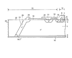
図29は、図28−1〜図28−3の方法で分離層が形成された従来の逆阻止型IGBTの要部断面図である。なお、図中の161はpウェル領域、162はp耐圧領域、163はエミッタ領域、164はゲート絶縁膜、165はゲート電極、166は層間絶縁膜、167はエミッタ電極、168はフィールド酸化膜、169はフィールドプレート、170はpコレクタ領域、171はコレクタ電極、172はダイシング面である。 FIG. 29 is a cross-sectional view of an essential part of a conventional reverse blocking IGBT in which a separation layer is formed by the method of FIGS. 28-1 to 28-3. In the figure, 161 is a p-well region, 162 is a p-voltage region, 163 is an emitter region, 164 is a gate insulating film, 165 is a gate electrode, 166 is an interlayer insulating film, 167 is an emitter electrode, 168 is a field oxide film, 169 is a field plate, 170 is a p collector region, 171 is a collector electrode, and 172 is a dicing surface.
図30(図30−1〜図30−3)は、従来の逆阻止型IGBTの分離層を形成する別の場合で、同図−1から同図−3は工程順に示した要部製造工程断面図である。これは、トレンチ(溝)を掘ってその側面に拡散層を形成して分離層を形成する方法である。数μmの厚い酸化膜173でエッチングマスクを形成する(図30−1)。つぎに、数百μm程度の深さのトレンチ174をドライエッチングで形成する(図30−2)。つぎに、気相拡散175にてトレンチ174の側壁へ不純物を導入して分離層176を形成する(図30−3)。
FIG. 30 (FIGS. 30-1 to 30-3) is another case of forming a separation layer of a conventional reverse blocking IGBT, and FIGS. It is sectional drawing. This is a method of forming a separation layer by digging a trench (groove) and forming a diffusion layer on its side surface. An etching mask is formed with a
図31は、図30−1〜図30−3の方法で分離層が形成された従来の逆阻止型IGBTの要部断面図である。トレンチ174に補強材177を充填した後、スクライブラインに沿ってダイシングして半導体ウェハ151からIGBTチップが切り出されて、逆阻止型IGBTができあがる。178はダイシング面である。
FIG. 31 is a fragmentary cross-sectional view of a conventional reverse blocking IGBT having a separation layer formed by the method of FIGS. 30-1 to 30-3. After filling the
このように、トレンチ174を掘ってその側面に分離層176を形成する方法としては、特許文献1〜3が開示されている。特許文献1において、デバイス上面から下側接合まで活性層を取り囲むようにトレンチを形成し、このトレンチの側面に拡散層を形成し、デバイスの下側接合の終端をデバイスの上面まで延在させて分離層を形成することが示されている。特許文献2および特許文献3において、これも特許文献1と同様に、デバイス上面から下側接合までトレンチを形成し、このトレンチの側面に拡散層を形成することで逆阻止能力のあるデバイスとしている。
As described above,
図28−1〜図28−3に示す逆阻止型IGBTの分離層の形成方法において、表面からボロンソース154(ボロンの液状の拡散源)を塗布し熱処理にてボロンを拡散し、数百μm程度の拡散深さの分離層155を形成するためには、高温、長時間の拡散処理を必要とする。このため、拡散炉を構成する石英ボード、石英管(石英チューブ)、石英ノズルなど石英治具のへたりや、ヒーターからの汚染、石英治具の失透現象による強度低下などを発生させてしまう。
In the method of forming the reverse blocking IGBT separation layer shown in FIGS. 28-1 to 28-3, boron source 154 (boron liquid diffusion source) is applied from the surface, and boron is diffused by heat treatment to be several hundred μm. In order to form the
またこの塗布拡散法による分離層155の形成では、マスク酸化膜(酸化膜152)の形成が必要となる。このマスク酸化膜は長時間のボロン拡散に耐えるようにするためには良質で厚い酸化膜が必要となる。この耐マスク性が高い、つまり良質なシリコン酸化膜を得る方法としては熱酸化の方法がある。
Further, in forming the
しかし、高温で長時間(例えば1300℃、200時間)のボロンによる分離層155の拡散処理においてボロンがマスク酸化膜を突き抜けないためには、膜厚が約2.5μmの熱酸化膜を形成させる必要がある。この膜厚2.5μmの熱酸化膜形成のためには、例えば1150℃の酸化温度において必要な酸化時間は、良質な酸化膜が得られるドライ(乾燥酸素雰囲気)酸化では、約200時間必要である。
However, in order to prevent boron from penetrating the mask oxide film in the diffusion treatment of the
膜質がやや劣るものの、ドライ酸化に比べて酸化時間が短くて済むウェットもしくはパイロジェニック酸化でも、約15時間と長い酸化時間を必要とする。さらにこれらの酸化処理中には、大量の酸素がシリコンウェハ中に導入されるために、酸素析出物や酸化誘起積層欠陥などの結晶欠陥が導入されたり、酸素ドナーが発生したりすることによるデバイス特性劣化や信頼性低下の弊害が生じる。 Wet or pyrogenic oxidation, which requires slightly shorter oxidation time than dry oxidation, requires a long oxidation time of about 15 hours, although the film quality is somewhat inferior. Furthermore, during these oxidation processes, a large amount of oxygen is introduced into the silicon wafer, so that crystal defects such as oxygen precipitates and oxidation-induced stacking faults are introduced, and oxygen donors are generated. Detrimental effects such as deterioration of characteristics and reliability occur.
さらに、ボロンソース154塗布後の拡散でも、通常は酸化雰囲気下で上記高温長時間の拡散処理が行われるため、ウェハ内に格子間酸素が導入され、この工程でも酸素析出物や酸素ドナー化現象、酸化誘起積層欠陥(OSF:Oxidation Induced Stacking Fault)や、スリップ転位など結晶欠陥が導入されてしまう。これら結晶欠陥が導入されたウェハに形成されたpn接合ではリーク電流が高くなってしまったり、ウェハ上に熱酸化により形成された絶縁膜の耐圧、信頼性が大幅に劣化することが知られている。また、拡散中に取り込まれた酸素がドナー化し、耐圧が低下するという弊害を生じさせる。
Further, even after diffusion after the
図28−1〜図28−3に示す分離層の形成方法では、ボロンによる拡散はマスク酸化膜の開口部から、シリコンバルクへとほぼ等方的に進行するため、深さ方向に200μmのボロン拡散を行う場合、必然的に横方向にもボロンは160μm拡散されてしまうため、デバイスピッチやチップサイズの縮小に対しての弊害を生じさせる。 In the method for forming the separation layer shown in FIGS. 28A to 28C, since the diffusion by boron proceeds substantially isotropically from the opening of the mask oxide film to the silicon bulk, boron having a depth of 200 μm is formed. When diffusion is performed, boron is inevitably diffused in the horizontal direction by 160 μm, which causes an adverse effect on device pitch and chip size reduction.
図30−1〜図30−3に示す分離層の形成方法では、ドライエッチングにてトレンチ174を形成し、形成したトレンチ174側壁にボロンを導入して分離層を形成する。その後、トレンチ174を絶縁膜などの補強材177で充填し、高アスペクト比のトレンチが形成できるため、図30−1〜図30−3の形成方法は図28−1〜図28−3の形成方法と比べてデバイスピッチの縮小に有利である。
30-1 to 30-3, the
しかし200μm程度のエッチングに要する時間は、典型的なドライエッチング装置を用いた場合、1枚あたり、100分程度の処理時間が必要であり、リードタイムの増加、メンテナンス回数の増加など弊害をもたらす。また、ドライエッチングによって深いトレンチを形成する場合、マスクとしてシリコン酸化膜(SiO2)を用いた場合、選択比が50以下なので、数μm程度の厚いシリコン酸化膜が必要とするため、コストの上昇や酸化誘起積層欠陥や酸素析出物などのプロセス誘起結晶欠陥導入による良品率低下という弊害を生じさせる。 However, the time required for etching of about 200 μm requires a processing time of about 100 minutes per sheet when a typical dry etching apparatus is used, which causes problems such as an increase in lead time and an increase in the number of maintenance. In addition, when a deep trench is formed by dry etching, when a silicon oxide film (SiO 2 ) is used as a mask, the selection ratio is 50 or less, so a thick silicon oxide film of about several μm is required, resulting in an increase in cost. As a result, there is a problem that the yield rate decreases due to the introduction of process-induced crystal defects such as oxidation-induced stacking faults and oxygen precipitates.
さらにドライエッチングによる高アスペクト比の深堀りトレンチを利用した分離層形成プロセスでは、図32に示すように、トレンチ内で薬液残渣179やレジスト残渣180などが発生し、歩留まりの低下や信頼性の低下など弊害を生じさせてしまう問題がある。通常、トレンチ側壁に対してリンやボロンなどのドーパントを導入する場合、トレンチ側壁が垂直となっているので、ウェハを斜めにしてイオン注入することによりトレンチ側壁へのドーパント導入を行っている。
Further, in the separation layer forming process using a deep trench with a high aspect ratio by dry etching, as shown in FIG. 32, a
しかし、アスペクト比の高いトレンチ側壁へのドーパント導入は、実効ドーズ量の低下(それに伴う注入時間の増加)、実効投影飛程の低下、スクリーン酸化膜によるドーズ量ロス、注入均一性の低下などの弊害を生じさせる。このため、アスペクト比の高いトレンチ内へ不純物を導入するための手法として、イオン注入の代わりにPH3(ホスフィン)やB2H6(ジボラン)などのガス化させたドーパント零囲気中にウェハを暴露させる気相拡散法が用いられるが、ドーズ量の精密制御性において、イオン注入法に比べて劣る。 However, introduction of dopants into trench sidewalls with a high aspect ratio can lead to a decrease in effective dose (according to an increase in implantation time), a decrease in effective projection range, a dose loss due to a screen oxide film, and a decrease in implantation uniformity. Cause harmful effects. For this reason, as a method for introducing impurities into a trench having a high aspect ratio, a wafer is placed in a gasified dopant zero atmosphere such as PH 3 (phosphine) or B 2 H 6 (diborane) instead of ion implantation. Although the gas phase diffusion method to be exposed is used, it is inferior to the ion implantation method in the precise controllability of the dose.
またアスペクト比の高いトレンチに絶縁膜を充填させる場合、トレンチ内にボイドと呼ばれる隙間ができてしまい、信頼性などの問題が発生する。そこで、本出願人は、異方性ドライエッチングによりトレンチを形成し、このトレンチの内面からボロンを拡散させて分離層を形成する方法を先に提案している(特願2004−36274号)。この提案によれば、ウェハの横方向へのボロンの広がりを抑えることができる。また、前記の特許文献1〜3の製造方法では、トレンチ内に補強材を充填してウェハをスクライブラインで切断して半導体チップ化する工程が必要となることが想定され、製造コストが高くなる。 Further, when an insulating film is filled in a trench having a high aspect ratio, a gap called a void is formed in the trench, which causes problems such as reliability. Therefore, the present applicant has previously proposed a method of forming a trench by anisotropic dry etching and diffusing boron from the inner surface of the trench to form a separation layer (Japanese Patent Application No. 2004-36274). According to this proposal, the spread of boron in the lateral direction of the wafer can be suppressed. Moreover, in the manufacturing method of the said patent documents 1-3, it is assumed that the process which fills a trench with a reinforcing material, cut | disconnects a wafer with a scribe line, and makes it a semiconductor chip becomes high, and manufacturing cost becomes high. .
この発明は、上述した従来技術による問題点を解消するため、信頼性が高く、デバイスピッチやチップサイズの小さい半導体装置を提供することを目的とする。また、この発明は、高温で長時間の拡散処理や、長時間の酸化処理を行わずに分離層を形成することができる半導体装置の製造方法を提供することを目的とする。さらに、この発明は、高い信頼性を有する半導体装置を低コストで製造することができる半導体装置の製造方法を提供することを目的とする。 An object of the present invention is to provide a semiconductor device having high reliability and a small device pitch and chip size in order to solve the above-described problems caused by the prior art. It is another object of the present invention to provide a method for manufacturing a semiconductor device that can form a separation layer without performing diffusion treatment for a long time at high temperature or oxidation treatment for a long time. Another object of the present invention is to provide a semiconductor device manufacturing method capable of manufacturing a highly reliable semiconductor device at low cost.
この発明にかかる半導体装置の製造方法は、第1導電型半導体基板の第1主面の表面領域に選択的に設けられた第2導電型ベース領域と、前記ベース領域の表面領域に選択的に設けられた第1導電型エミッタ領域と、前記ベース領域の、前記半導体基板と前記エミッタ領域に挟まれた部分の表面上に設けられたゲート絶縁膜、および該ゲート絶縁膜上に設けられたゲート電極を含むMOSゲート構造と、前記エミッタ領域および前記ベース領域に接触するエミッタ電極と、前記半導体基板の第2主面の表面層に設けられた第2導電型コレクタ層と、前記コレクタ層に接触するコレクタ電極と、前記MOSゲート構造を囲み、かつ前記第1主面から前記第2主面に対して傾斜して前記第2主面まで至り、前記コレクタ層に連結された第2導電型分離層と、を有し、前記第1主面および前記第2主面は、{100}面であり、前記半導体基板に形成された溝の側壁は、{111}面である半導体装置を製造するにあたって、第1導電型半導体基板の第1主面を所望のパターンのマスクで被覆する工程と、前記半導体基板の、前記マスクにより被覆されていない部分をアルカリ溶液に接触させて湿式異方性エッチングを行い、前記半導体基板に、断面形状がV字状または台形状である溝を形成する工程と、前記溝の側壁に第2導電型不純物を導入して第2導電型分離層を形成する工程と、を含み、前記溝の側壁に第2導電型不純物を導入した後に、前記第1主面に半導体膜を堆積して前記溝を当該半導体膜で埋め、その後に熱処理を行うことを特徴とする。A method for manufacturing a semiconductor device according to the present invention includes a second conductivity type base region selectively provided in a surface region of a first main surface of a first conductivity type semiconductor substrate, and a surface region of the base region. A first conductivity type emitter region provided; a gate insulating film provided on a surface of a portion of the base region sandwiched between the semiconductor substrate and the emitter region; and a gate provided on the gate insulating film A MOS gate structure including an electrode; an emitter electrode in contact with the emitter region and the base region; a second conductivity type collector layer provided on a surface layer of a second main surface of the semiconductor substrate; and a contact with the collector layer And a second conductivity type surrounding the MOS gate structure and inclined from the first main surface to the second main surface and connected to the collector layer A semiconductor device is manufactured, wherein the first main surface and the second main surface are {100} planes, and the side walls of the grooves formed in the semiconductor substrate are {111} planes. In the process, the first main surface of the first conductivity type semiconductor substrate is covered with a mask having a desired pattern, and the portion of the semiconductor substrate that is not covered with the mask is brought into contact with an alkaline solution to perform wet anisotropy. Etching to form a groove having a V-shaped or trapezoidal cross-sectional shape on the semiconductor substrate, and introducing a second conductivity type impurity into the side wall of the groove to form a second conductivity type separation layer. A semiconductor film is deposited on the first main surface, the groove is filled with the semiconductor film, and then a heat treatment is performed after introducing a second conductivity type impurity into the sidewall of the groove. And
この発明にかかる半導体装置の製造方法は、上述した発明において、前記溝は、54.7°の角度で傾斜するよう形成し、前記側壁にイオン注入法により第2導電型不純物を導入することを特徴とする。この発明にかかる半導体装置の製造方法は、上述した発明において、前記第1主面側にゲート絶縁膜およびゲート電極を含むMOSゲート構造を形成した後に、前記溝の形成と第2導電型不純物の導入を順次行って前記第2導電型分離層を形成することを特徴とする。この発明にかかる半導体装置の製造方法は、上述した発明において、前記第1主面側にゲート絶縁膜およびゲート電極を含むMOSゲート構造を形成し、エミッタ電極を形成した後に、前記溝の形成と第2導電型不純物の導入を順次行って前記第2導電型分離層を形成することを特徴とする。In the semiconductor device manufacturing method according to the present invention, in the above-described invention, the groove is formed so as to be inclined at an angle of 54.7 °, and the second conductivity type impurity is introduced into the sidewall by an ion implantation method. Features. According to a method of manufacturing a semiconductor device according to the present invention, in the above-described invention, after forming a MOS gate structure including a gate insulating film and a gate electrode on the first main surface side, formation of the trench and formation of the second conductivity type impurity are performed. The second conductivity type separation layer is formed by sequentially introducing the second conductivity type separation layer. According to a method of manufacturing a semiconductor device according to the present invention, in the above-described invention, a MOS gate structure including a gate insulating film and a gate electrode is formed on the first main surface side, and an emitter electrode is formed. The second conductivity type separation layer is formed by sequentially introducing second conductivity type impurities.
この発明にかかる半導体装置の製造方法は、上述した発明において、前記第1主面側にゲート絶縁膜およびゲート電極を含むMOSゲート構造を形成し、エミッタ電極を形成し、前記第1主面側の表面保護膜を形成した後に、前記溝の形成と第2導電型不純物の導入を順次行って前記第2導電型分離層を形成することを特徴とする。According to a method of manufacturing a semiconductor device according to the present invention, in the above-described invention, a MOS gate structure including a gate insulating film and a gate electrode is formed on the first main surface side, an emitter electrode is formed, and the first main surface side is formed. After forming the surface protective film, the formation of the groove and the introduction of the second conductivity type impurity are sequentially performed to form the second conductivity type separation layer.
上述した発明によれば、アルカリ溶液による湿式異方性エッチングにおいて、エッチングマスクを、マスク選択比が非常に高いシリコン酸化膜やシリコン窒化膜(SiAccording to the above-described invention, in wet anisotropic etching with an alkaline solution, an etching mask is used as a silicon oxide film or silicon nitride film (Si 3Three NN 4Four )で形成することによって、エッチングマスクを薄くすることができる。例えば、エッチングマスクとしてシリコン酸化膜を用い、エッチング溶液として水酸化カリウム(KOH)水溶液を用いる場合、マスク選択比は1:350〜500と非常に大きいので、マスク酸化膜であるシリコン酸化膜の厚さを非常に小さくすることができる。従って、熱酸化によりマスク酸化膜を形成する際の酸化温度を低くし、また酸化時間を大幅に短くすることができるので、従来のリードタイムの増加という問題や、酸化時の酸素導入に起因する結晶欠陥の発生という問題を抑制することができる。The etching mask can be made thinner. For example, when a silicon oxide film is used as an etching mask and a potassium hydroxide (KOH) aqueous solution is used as an etching solution, the mask selectivity is as large as 1: 350 to 500, so the thickness of the silicon oxide film that is the mask oxide film is large. Can be made very small. Therefore, the oxidation temperature when forming the mask oxide film by thermal oxidation can be lowered, and the oxidation time can be greatly shortened, resulting in the problem of the conventional increase in lead time and the introduction of oxygen during oxidation. The problem of generation of crystal defects can be suppressed.
また、化学気相成長法(CVD)により形成したシリコン酸化膜は、熱酸化膜よりも膜質(耐マスク性)がやや劣るが、エッチングマスクとして十分なマスク選択比を有しているので、減圧CVD法やプラズマCVD法により形成されたTEOS膜またはシリコン窒化膜などをエッチングマスクとして用いることもできる。この場合には、CVDの形成温度が200〜680℃と低温であるので、ウェハ形成プロセスの後半、すなわちMOSゲート構造を形成した後や、エミッタ電極を形成した後や、表面保護膜を形成した後などに、分離層を形成するための溝を形成することができる。In addition, the silicon oxide film formed by chemical vapor deposition (CVD) is slightly inferior in film quality (mask resistance) to the thermal oxide film, but has a sufficient mask selection ratio as an etching mask. A TEOS film or a silicon nitride film formed by a CVD method or a plasma CVD method can also be used as an etching mask. In this case, since the CVD forming temperature is as low as 200 to 680 ° C., the latter half of the wafer forming process, that is, after forming the MOS gate structure, forming the emitter electrode, or forming the surface protective film. A groove for forming the separation layer can be formed later.
また、アルカリ溶液による湿式異方性エッチングでは、エッチングレートを非常に高く設定することができる。例えば、54重量%濃度の水酸化カリウム水溶液を用いて、110℃でエッチングを行う場合、エッチングレートは、おおよそ8μm/分である。加えて、湿式エッチングでは、数〜数十枚のウェハを同時に処理するバッチ式と呼ばれる方法でエッチングを行うことができるので、リードタイムの短縮やコストの削減において非常に大きな効果を奏する。Moreover, in wet anisotropic etching with an alkaline solution, the etching rate can be set very high. For example, when etching is performed at 110 ° C. using a 54 wt% potassium hydroxide aqueous solution, the etching rate is approximately 8 μm / min. In addition, in wet etching, etching can be performed by a method called a batch method in which several to several tens of wafers are processed at the same time, which is very effective in reducing lead time and cost.
また、アルカリ溶液による湿式異方性エッチングでは、エッチング温度は、200℃以下である。従って、サーマルバジェットが非常に小さくなり、活性領域のドーパントプロファイルへの影響がない。また、湿式異方性エッチングにより溝を形成する前に、アルミニウム(Al)などの比較的低融点の金属や、熱に弱い材料がウェハ上に形成されていても、エッチングを行ったことによるそれらに対する影響はない。In wet anisotropic etching with an alkaline solution, the etching temperature is 200 ° C. or lower. Therefore, the thermal budget is very small and does not affect the dopant profile of the active region. In addition, even if a relatively low melting point metal such as aluminum (Al) or a heat-sensitive material is formed on the wafer before the grooves are formed by wet anisotropic etching, those due to the etching are performed. There is no impact on
また、アルカリ溶液による湿式異方性エッチングによって溝を形成した後に、ボロンのイオン注入を行うことによって、従来よりも熱処理温度を低くすることができ、また熱処理時間を短くすることができるので、分離層を形成する際のリードタイムの削減と、それに伴う良品率の改善という効果が得られる。また、溝(トレンチ)の側壁のテーパー角度が、ドライエッチングによって形成されたトレンチに比べて非常に大きいので、イオン注入における従来の弊害、すなわち実効ドーズ量の低下、スクリーン酸化膜によるドーズ量ロス、イオンビームの反射や再放出によるドーズ量ロス、実効投影飛程の低下などを抑制することができる。さらに、溝の側壁のテーパー角度が大きいことにより、溝内の薬液や残渣を容易に除去することができるので、歩留まりと信頼性の向上に大きな効果がある。In addition, after forming grooves by wet anisotropic etching with an alkaline solution, boron ion implantation is performed, so that the heat treatment temperature can be lowered and the heat treatment time can be shortened. The effect of reducing the lead time when forming the layer and improving the yield rate is obtained. Further, since the taper angle of the side wall of the groove (trench) is much larger than that of a trench formed by dry etching, conventional disadvantages in ion implantation, that is, reduction in effective dose amount, loss of dose amount due to screen oxide film, It is possible to suppress a dose loss due to ion beam reflection and re-emission, a decrease in effective projection range, and the like. Furthermore, since the taper angle of the side wall of the groove is large, the chemical solution and residue in the groove can be easily removed, which has a great effect on yield and reliability.
また、アルカリ溶液による異方性エッチングでは、例えば(100)面を主面とするシリコンウェハを用いて、<110>方向に等価な結晶方向である{110}方向にマスクアライメントを配置する場合、溝の側壁のテーパー角度が54.7°に固定される。従って、プロセスのばらつきが少ないという効果がある。また、溝の側壁のテーパー角度が54.7°に固定されることによって、エッチングが進行して溝の断面形状がV字状になった時点で、エッチングの進行が自動的に停止する。つまり、V字状の溝の深さは、エッチングマスクの開口幅によって決定されるので、溝の深さのばらつきが従来よりも非常に小さくなるという効果を奏する。Further, in anisotropic etching with an alkaline solution, for example, when a mask alignment is arranged in the {110} direction, which is a crystal direction equivalent to the <110> direction, using a silicon wafer having a (100) plane as a main surface, The taper angle of the groove sidewall is fixed at 54.7 °. Therefore, there is an effect that the process variation is small. Further, by fixing the taper angle of the side wall of the groove to 54.7 °, the progress of the etching is automatically stopped when the etching progresses and the cross-sectional shape of the groove becomes a V-shape. In other words, since the depth of the V-shaped groove is determined by the opening width of the etching mask, there is an effect that the variation in the depth of the groove is much smaller than the conventional one.
この発明にかかる半導体装置の製造方法は、半導体ウェハの第1主面側に複数の拡散層と第1主電極および制御電極を形成する工程と、前記半導体ウェハの第2主面を研削して該半導体ウェハを薄くする工程と、該薄い半導体ウェハの第2主面側に拡散層と該拡散層と接する第2主電極とを形成する工程と、前記第2主電極を接着層を介して支持基板に接着する工程と、前記第1主面側から前記第2主面側の拡散層に達する溝を形成する工程と、該溝の側壁面の全域に前記第2主面側の拡散層と同一導電型の分離層を前記第2主面側の拡散層と接するように形成する工程と、前記接着層を前記薄い半導体ウェハから剥離して、前記半導体ウェハを半導体チップ化する工程と、を含むことを特徴とする。A method of manufacturing a semiconductor device according to the present invention includes a step of forming a plurality of diffusion layers, a first main electrode, and a control electrode on a first main surface side of a semiconductor wafer, and grinding a second main surface of the semiconductor wafer. A step of thinning the semiconductor wafer, a step of forming a diffusion layer and a second main electrode in contact with the diffusion layer on the second main surface side of the thin semiconductor wafer, and the second main electrode through an adhesive layer A step of adhering to a support substrate, a step of forming a groove reaching the diffusion layer on the second main surface side from the first main surface side, and a diffusion layer on the second main surface side in the entire side wall surface of the groove Forming a separation layer of the same conductivity type so as to be in contact with the diffusion layer on the second main surface side, peeling the adhesive layer from the thin semiconductor wafer, and converting the semiconductor wafer into a semiconductor chip; It is characterized by including.
この発明にかかる半導体装置の製造方法は、上述した発明において、前記接着層が、少なくとも発泡テープで構成されることを特徴とする。この発明にかかる半導体装置の製造方法は、上述した発明において、前記薄い半導体ウェハの第1主面の結晶面が{100}面であり、前記溝の表面の結晶面が{111}面であることを特徴とする。この発明にかかる半導体装置の製造方法は、上述した発明において、前記溝が、湿式異方性エッチングで形成されることを特徴とする。The method for manufacturing a semiconductor device according to the present invention is characterized in that, in the above-described invention, the adhesive layer is composed of at least a foamed tape. In the semiconductor device manufacturing method according to the present invention, in the above-described invention, the crystal surface of the first main surface of the thin semiconductor wafer is a {100} plane, and the crystal plane of the surface of the groove is a {111} plane. It is characterized by that. The method for manufacturing a semiconductor device according to the present invention is characterized in that, in the above-described invention, the groove is formed by wet anisotropic etching.
この発明にかかる半導体装置の製造方法は、上述した発明において、前記分離層が、イオン注入と500℃以下の低温アニールで形成されることを特徴とする。この発明にかかる半導体装置の製造方法は、上述した発明において、前記分離層が、イオン注入とレーザーアニールで形成されることを特徴とする。この発明にかかる半導体装置の製造方法は、上述した発明において、前記溝の側壁面に照射されるレーザーの照射エネルギー密度が側壁面全域に亘って一定であることを特徴とする。The method for manufacturing a semiconductor device according to the present invention is characterized in that, in the above-described invention, the separation layer is formed by ion implantation and low-temperature annealing at 500 ° C. or lower. The method for manufacturing a semiconductor device according to the present invention is characterized in that, in the above-described invention, the separation layer is formed by ion implantation and laser annealing. The method for manufacturing a semiconductor device according to the present invention is characterized in that, in the above-described invention, the irradiation energy density of the laser irradiated on the side wall surface of the groove is constant over the entire side wall surface.
この発明にかかる半導体装置の製造方法は、上述した発明において、前記レーザーの照射エネルギー密度が1.5Joule/cmThe method of manufacturing a semiconductor device according to this invention is the above-described invention, wherein the irradiation energy density of the laser is 1.5 Joule / cm. 22 以上であることを特徴とする。この発明にかかる半導体装置の製造方法は、上述した発明において、前記溝の底面までの深さが、1mm以下であることを特徴とする。It is the above. The semiconductor device manufacturing method according to the present invention is characterized in that, in the above-described invention, the depth to the bottom surface of the groove is 1 mm or less.
上述した発明によれば、逆阻止型半導体チップを構成する表面構造、裏面構造を形成した薄い半導体ウェハを支持基板に貼り付け、スクライブラインとなる溝(トレンチ)を薄い半導体ウェハに形成し、このトレンチの側面に分離層を形成し、半導体ウェハを支持基板から剥がして半導体チップとすることで、従来のようなダイシング工程が削減でき、分離層形成に塗布拡散法を用いないので、酸素起因による特性劣化の影響が低減でき、低コストで、高い信頼性の逆阻止型の半導体装置を提供することができる。また、分離層の活性化に低温アニールやレーザーアニールを用いることで一様で拡散深さの浅い分離層とすることができて、従来の塗布拡散法に比べて、分離層の半導体チップに占める占有面積を小さくできてデバイスピッチを縮小することができる。According to the above-described invention, a thin semiconductor wafer on which a front surface structure and a back surface structure constituting a reverse blocking semiconductor chip are formed is attached to a support substrate, and a groove (trench) serving as a scribe line is formed on the thin semiconductor wafer. By forming a separation layer on the side surface of the trench and peeling the semiconductor wafer from the support substrate to form a semiconductor chip, the conventional dicing process can be reduced, and the coating diffusion method is not used for forming the separation layer. An influence of characteristic deterioration can be reduced, and a low-reliability reverse-blocking semiconductor device can be provided at low cost. Also, by using low-temperature annealing or laser annealing for the activation of the separation layer, it is possible to obtain a separation layer having a uniform and shallow diffusion depth, which occupies the semiconductor chip of the separation layer as compared with the conventional coating diffusion method. The occupied area can be reduced and the device pitch can be reduced.
この発明にかかる半導体装置の製造方法は、半導体ウェハの第1主面側に複数の拡散層と第1主電極および制御電極を形成する工程と、前記半導体ウェハの第2主面を研削して該半導体ウェハを薄くする工程と、該薄い半導体ウェハの第2主面側に拡散層と該拡散層と接する第2主電極とを形成する工程と、前記第2主電極を接着層を介して支持基板に接着する工程と、前記第1主面側から前記第2主面側の拡散層に達する溝を形成する工程と、該溝の側壁面の全域に不純物をイオン注入し、その不純物注入領域にレーザー照射を行って前記第2主面側の拡散層と同一導電型の分離層を前記第2主面側の拡散層と接するように形成する工程と、前記溝の底面にレーザー照射を行って前記第2主面側の拡散層とその下の前記第2主電極を切断する工程と、前記接着層を前記薄い半導体ウェハから剥離して、前記半導体ウェハを半導体チップ化する工程と、を含むことを特徴とする。A method of manufacturing a semiconductor device according to the present invention includes a step of forming a plurality of diffusion layers, a first main electrode, and a control electrode on a first main surface side of a semiconductor wafer, and grinding a second main surface of the semiconductor wafer. A step of thinning the semiconductor wafer, a step of forming a diffusion layer and a second main electrode in contact with the diffusion layer on the second main surface side of the thin semiconductor wafer, and the second main electrode through an adhesive layer A step of bonding to the support substrate, a step of forming a groove reaching the diffusion layer on the second main surface side from the first main surface side, and an ion implantation of impurities over the entire side wall surface of the groove, and the impurity implantation Irradiating the region with a laser to form a separation layer having the same conductivity type as the diffusion layer on the second main surface side so as to be in contact with the diffusion layer on the second main surface side; To cut the diffusion layer on the second main surface side and the second main electrode therebelow A step, by peeling off the adhesive layer from the thin semiconductor wafer, characterized in that it comprises a and a step of forming a semiconductor chip of the semiconductor wafer.
この発明にかかる半導体装置の製造方法は、上述した発明において、前記分離層を形成する際のレーザー照射と、前記第2主面側の拡散層と前記第2主電極を切断する際のレーザー照射を、同一のレーザー照射装置により行うことを特徴とする。The method of manufacturing a semiconductor device according to the present invention includes the laser irradiation for forming the separation layer and the laser irradiation for cutting the diffusion layer on the second main surface side and the second main electrode in the above-described invention. Is performed by the same laser irradiation apparatus.
上述した発明によれば、デバイスを先に形成してから、分離層を形成し、空乏層を制御するためにその分離層と第2主面側の拡散層をつなぐ必要があるが、支持基板を貼り付けて分離層の形成を行うことによって、分離層形成のためにトレンチを形成しても、そのトレンチ形成部のイオン注入工程とアニール工程が終了するまでにウェハがチップ状にばらばらになってしまうことはない。また、デバイスと支持基板との接着に、発泡テープとUVテープを貼り合わせた両面粘着テープを用い、デバイス面に発泡テープを貼り付け、支持基板にUVテープを貼り付けることによって、アニール処理後に容易にデバイスから両面粘着テープを発泡剥離させることができる。According to the above-described invention, after forming the device first, it is necessary to form the separation layer and connect the separation layer and the diffusion layer on the second main surface side in order to control the depletion layer. Even if a trench is formed for forming the separation layer, the wafer is separated into chips until the ion implantation process and the annealing process of the trench formation part are completed. There is no end to it. In addition, a double-sided adhesive tape with a foam tape and UV tape bonded to the device and the support substrate is used. The foam tape is attached to the device surface, and the UV tape is attached to the support substrate. The double-sided adhesive tape can be foamed and peeled from the device.
また、イオン注入後のアニール工程をレーザーアニールにすることによって、瞬時にシリコンの融点に近い温度まで活性化することができるので、分離層を形成するためにイオン注入したドーパント(例えば、BやAl等のp型ドーパント)を500℃以下の低温炉アニールよりも高活性化することができる。その際、表面から数μmまでの距離しか活性化しないので、既に形成された表面電極への影響はない。Also, by performing laser annealing as the annealing step after ion implantation, activation can be instantaneously made to a temperature close to the melting point of silicon, so that an ion-implanted dopant (for example, B or Al) can be formed to form a separation layer. P-type dopant) can be activated more than low temperature furnace annealing at 500 ° C. or lower. At that time, since only a distance of several μm from the surface is activated, there is no influence on the already formed surface electrode.
また、レーザーアニール後に、分離層の底面の拡散層と第2主電極をレーザー照射により切断してから、両面粘着テープの発泡剥離を行って個々のチップにするので、分離層の下で第2主電極を過不足なくきれいに切断することができる。従って、第2主電極がチップ端面から少し飛び出た状態で残ったり、第2主電極が分離層の下の部分で欠けてしまったりすることがない。また、第2主電極の切断面にバリ等が残らないので、きれいなチップ断面(切断面)を得ることができる。In addition, after the laser annealing, the diffusion layer on the bottom surface of the separation layer and the second main electrode are cut by laser irradiation, and then the double-sided adhesive tape is foamed and peeled into individual chips. The main electrode can be cut cleanly without excess or deficiency. Therefore, the second main electrode does not remain in a state of slightly protruding from the end surface of the chip, and the second main electrode is not chipped in a portion below the separation layer. Moreover, since no burrs or the like remain on the cut surface of the second main electrode, a clean chip cross section (cut surface) can be obtained.
上述した発明によれば、レーザー照射装置は、レーザーアニール工程ではイオン注入層の活性化として作用し、レーザーダイシング工程では加工モードで加工するように作用する。第2主電極の厚さは数μmと薄いので、レーザーダイシングの時間も短くて済み、通常のダイシングを使うよりも効果的である。また、この2つの工程は、同じ装置で照射エネルギー密度を変えることにより連続工程として実施することができる。従って、一台の装置で2つの工程を連続して行うことができるので、投資コストを抑えることができる。According to the above-described invention, the laser irradiation apparatus acts as activation of the ion implantation layer in the laser annealing process, and acts to process in the processing mode in the laser dicing process. Since the thickness of the second main electrode is as thin as several μm, the laser dicing time can be shortened, which is more effective than using normal dicing. Moreover, these two processes can be implemented as continuous processes by changing the irradiation energy density with the same apparatus. Therefore, since two processes can be performed continuously with one apparatus, the investment cost can be suppressed.
本発明にかかる半導体装置の製造方法によれば、アルカリ溶液による湿式異方性エッチングによりシリコン半導体基板に溝を形成し、この溝の側壁に不純物をイオン注入することによって、高温で長時間の拡散処理や、長時間の酸化処理を行わずに分離層を形成することができる。また、支持基板を貼り付けて分離層の形成を行うことによって、第2主面側の拡散層につながる分離層を容易に形成することができる。さらに、レーザー照射によるダイシングを行ってから支持基板を取り外すことにより、分離層の下で第2主電極を過不足なくきれいに切断することができる。従って、信頼性が高く、デバイスピッチやチップサイズの小さい半導体装置が低コストで得られるという効果を奏する。 According to the manufacturing method of the semiconductor equipment according to the present invention, a groove is formed in the silicon semiconductor substrate by wet anisotropic etching with an alkaline solution, by ion-implanting an impurity into the side wall of the groove, a long time at high temperatures The separation layer can be formed without performing diffusion treatment or long-time oxidation treatment. Moreover, the separation layer connected to the diffusion layer on the second main surface side can be easily formed by attaching the support substrate and forming the separation layer. Further, by removing the support substrate after dicing by laser irradiation, the second main electrode can be cleanly cut under the separation layer without excess or deficiency. Therefore, there is an effect that a semiconductor device with high reliability and a small device pitch and chip size can be obtained at low cost.
以下に添付図面を参照して、この発明にかかる半導体装置の製造方法の好適な実施の形態を詳細に説明する。ここでは、本発明を逆阻止型IGBTに適用した例について説明する。本明細書および添付図面においては、nまたはpを冠記した層や領域では、それぞれ電子または正孔が多数キャリアであることを意味する。また、nまたはpに付す「+」および「-」は、それぞれ比較的高不純物濃度および比較的低不純物濃度であることを意味する。なお、以下の説明および添付図面において、同一の符号を付した構成は同様の構成であるので、重複する説明を省略する。 With reference to the accompanying drawings, illustrating a preferred embodiment of the manufacturing method of the semiconductor equipment according to the present invention in detail. Here, an example in which the present invention is applied to a reverse blocking IGBT will be described. In the present specification and the accompanying drawings, it means that electrons or holes are majority carriers in layers and regions with n or p, respectively. Further, “ + ” and “ − ” attached to n or p mean a relatively high impurity concentration and a relatively low impurity concentration, respectively. Note that, in the following description and the accompanying drawings, the same reference numerals are assigned to the same components, so that the duplicate description is omitted.
実施の形態1.
図1は、本発明の実施の形態1にかかる逆阻止型IGBTの構成を示す断面図である。図1に示すように、高比抵抗のn-シリコン半導体基板1の第1主面15に、pベース領域2が選択的に複数形成されている。基板裏面側の第2主面16には、p+コレクタ層3が形成されている。pベース領域2とp+コレクタ層3とによって基板厚さ方向に挟まれる領域は、もともとn-シリコン半導体基板1であり、nベース領域となる。特に限定しないが、n-シリコン半導体基板1の厚さ、すなわち第1主面15から第2主面16までの寸法は、例えば200μmである。
FIG. 1 is a cross-sectional view illustrating a configuration of a reverse blocking IGBT according to a first embodiment of the present invention. As shown in FIG. 1, a plurality of
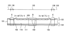
矢印で示す活性領域14において、pベース領域2内の表面層には、n+エミッタ領域4が選択的に形成されている。この活性領域14の外側には、プレーナ型pn接合表面の終端構造の一種として、矢印で示す耐圧構造13が形成されており、このIGBTの順方向阻止耐圧を確保している。この耐圧構造13は、第1主面15内で活性領域14の外側にあって、n-シリコン半導体基板1の表面層にリング状に形成されるp+半導体領域11のガードリング、酸化膜12および金属膜24のフィールドプレート等を複数段組み合わせて作られている。
In the
n+エミッタ領域4とnベース領域(n-シリコン半導体基板1)とに挟まれたpベース領域2の表面と、複数のpベース領域2間のnベース領域の表面には、ゲート絶縁膜5を介してそれぞれゲート電極6が形成されている。n+エミッタ領域4の表面は、エミッタ電極8により被覆されている。p+コレクタ層3の表面は、コレクタ電極9により被覆されている。エミッタ電極8とゲート電極6との間には、層間絶縁膜7が設けられている。
A gate insulating film 5 is formed on the surface of the
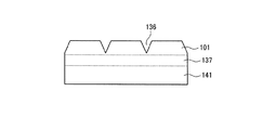
耐圧構造13の外側には、p+分離層20が形成されている。p+分離層20は、第1主面15から形成された溝(トレンチ)21の側壁に沿って形成されている。この溝21の側壁は、第2主面16に対しておおよそ54.7°の角度で傾斜している。従って、p+分離層20は、断面形状が帯状で、第2主面16に対しておおよそ54.7°の角度で傾斜している。
A p + isolation layer 20 is formed outside the
p+分離層20とダイシング等による切断面25との間に形成された充填領域22は、SOG(スピンオングラス)やBPSG、ポリシラザン、ポリイミドなどの絶縁膜、もしくはポリシリコンやエピタキシャルシリコンなどの半導体膜によって充填された領域である。この充填領域22は、切断面25で切断される前の溝21内に充填されたものである。p+分離層20が設けられていることによって、逆バイアス時にpn接合の前後に広がる空乏層が切断面25およびその周辺のダメージ領域に広がるのを防ぐことができるので、十分な逆耐圧を得ることができる。
The filling
本実施の形態では、p+分離層20を形成するために、アルカリ溶液による湿式異方性エッチングを行うことによって、n-シリコン半導体基板1に、断面形状がV字状または台形状であり、かつ側壁がn-シリコン半導体基板1の第2主面16に対しておおよそ54.7°の角度で傾斜する溝21を形成する。この溝21の形成方法について、図5〜図9を参照しながら説明する。図5は、アルカリ溶液によるシリコンの湿式異方性エッチングを説明するための断面斜視図である。図5において、符号31は、シリコンウェハであり、符号32は、シリコン酸化膜やシリコン窒化膜よりなるエッチングマスクである。
In the present embodiment, by performing wet anisotropic etching with an alkaline solution to form the p + isolation layer 20, the n −
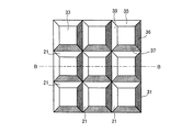
また、図6および図8は、アルカリ溶液によるシリコンの湿式異方性エッチングによって形成されたチップ9個分の溝のパターンを示す平面図である。図7および図9は、それぞれ図6の切断線A−Aおよび図8の切断線B−Bにおける構成を示す断面図である。図6〜図9において、符号33は、デバイスの活性領域14となる(100)面であり、符号34は、エッチングにより露出した(100)面であり、符号35、36、37および38は、それぞれ溝21の側壁である(111)面、(11−1)面、(1−1−1)面および(1−11)面である。なお、本明細書では、ミラー指数の表記において、“−”はその直後の指数につくバーを意味する。
6 and 8 are plan views showing patterns of grooves for nine chips formed by wet anisotropic etching of silicon with an alkaline solution. 7 and 9 are cross-sectional views showing configurations at a cutting line AA in FIG. 6 and a cutting line BB in FIG. 8, respectively. 6-9, the code |
シリコンの湿式異方性エッチング溶液には、水酸化カリウム、ヒドラジン、エチレンジアミン、アンモニア、TMAH(水酸化テトラメチルアンモニウム)などの水溶液を用いる。これらアルカリ溶液を用いたシリコンのエッチングには、シリコンの面方位によってエッチングレートが異なるという特性、すなわち異方性がある。具体的には、例えば水酸化カリウム溶液を用いた場合、(110)面および(100)面のエッチングレートは、それぞれ(111)面のエッチングレートの600倍および400倍である。つまり、事実上、(111)面に等価な結晶面でエッチングがストップする。 An aqueous solution of potassium hydroxide, hydrazine, ethylenediamine, ammonia, TMAH (tetramethylammonium hydroxide), or the like is used for the wet anisotropic etching solution of silicon. Etching of silicon using these alkaline solutions has a characteristic that the etching rate varies depending on the plane orientation of silicon, that is, anisotropy. Specifically, for example, when a potassium hydroxide solution is used, the etching rates of the (110) plane and the (100) plane are 600 times and 400 times the etching rate of the (111) plane, respectively. That is, the etching actually stops at a crystal plane equivalent to the (111) plane.
そのため、(100)ウェハ上に予め{110}方位に沿ってエッチングマスクを形成してエッチングを行えば、V字状の溝やピラミッド形のピット、あるいはピラミッド形の空洞構造を形成することができるということが知られている。また、エッチングマスクの開口幅やエッチング時間を調整することにより、任意の深さと任意の大きさのV字状や台形状の溝、あるいはピラミッド形のピットを形成することができるということが知られている。 Therefore, if an etching mask is previously formed on the (100) wafer along the {110} direction and etching is performed, a V-shaped groove, a pyramidal pit, or a pyramidal cavity structure can be formed. It is known that. It is also known that V-shaped or trapezoidal grooves or pyramid-shaped pits of any depth and size can be formed by adjusting the opening width and etching time of the etching mask. ing.
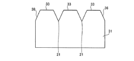
エッチングを途中で停止させた場合には、図5〜図7に示すように、断面が逆台形状の溝21を形成することができる。この場合には、溝21の側壁となる(111)面35、(11−1)面36、(1−1−1)面37および(1−11)面38と、エッチングにより露出した(100)面34とのなす角度は、おおよそ125.3゜であり、後述するV字状溝の底部の角度よりも大きい。従って、V字状溝の場合よりも、レジストや薬液の残渣を取り除きやすく、また容易に溝21内に空洞を生じさせずに絶縁膜を埋め込むことができる。
When the etching is stopped halfway, a
エッチングをさらに進行させると、溝21の側壁の{111}面が増加する一方で、溝21の底部の(100)面34が減少していく。そして、最終的には、図8および図9に示すように、溝21の底部の(100)面34が消滅し、相対峙する両側の{111}面がおおよそ70.6°の角度をなして交差すると、それ以上のエッチングが実質的に停止する。このため、エッチング時間がばらついても、V字状の溝21の深さにばらつきは生じない。つまり、V字状の溝21の深さは、エッチング時間に応じて決まるのではなく、エッチングマスク32の開口幅に応じて決まる。
When the etching further proceeds, the {111} plane of the side wall of the
具体的には、V字状の溝21の深さは、エッチングマスク32の開口幅の1/2にtan54.7°を乗じた値となる。逆に、所望の深さのV字状の溝21を形成するには、エッチングマスク32の開口幅を、溝21の深さに2/tan54.7°を乗じた値とすればよい。例えば、溝の深さを200μmにする場合には、エッチングマスク32の開口幅を283μmにすればよいので、デバイスピッチの縮小化に有利である。ただし、この場合には、溝21の底部の角度がおおよそ70.6°とやや鋭角的であるため、水素アニール処理、角部の丸め酸化処理またはCDE(ケミカルドライエッチング)処理などを行って、角部が丸みを帯びるようにしておくとよい。
Specifically, the depth of the V-shaped
つぎに、図1に示す構成の逆阻止型IGBTの製造プロセスについて、図2(図2−1〜図2−3)を参照しながら説明する。まず、例えば熱酸化によりシリコンウェハ31上にマスク酸化膜30を形成する(図2−1)。アルカリ溶液によるシリコンの湿式異方性エッチングでは、エッチングマスク選択比が大きいため、マスク酸化膜30を非常に薄くすることができる。熱酸化膜に対して膜質(耐マスク性)がやや劣るが、CVDで形成したシリコン酸化膜でも十分なエッチングマスク選択比が得られるので、減圧CVD法やプラズマCVD法によりTEOS膜などを形成し、これをマスク酸化膜30としてもよい。
Next, a manufacturing process of the reverse blocking IGBT having the configuration shown in FIG. 1 will be described with reference to FIG. 2 (FIGS. 2-1 to 2-3). First, the
次いで、マスク酸化膜30のパターニングおよびエッチングを行って、所望のパターンのエッチングマスク32を形成する。そして、上述したアルカリ溶液によるシリコンの湿式異方性エッチングを行い、台形状(または、図2−2において点線で示すV字状)の溝21を形成する。その後、溝21の側壁に、例えばボロンをイオン注入法により導入する(図2−2)。その際、溝21の側壁のテーパー角度がおおよそ54.7°と非常に大きいので、シリコンウェハ31を傾けずに溝21の側壁に不純物を注入することができる。つまり、チルト角度0°でもってイオン注入を行うことができる。
Next, patterning and etching of the
この場合には、1回のイオン注入によって、(111)面35、(11−1)面36、(1−1−1)面37および(1−11)面38の4つの側壁に同時に不純物を注入することができるので、簡便である。ただし、通常のトレンチ側壁へのイオン注入のように、シリコンウェハ31を斜めに傾けて、(111)面35、(11−1)面36、(1−1−1)面37および(1−11)面38の4つの側壁ごとに不純物を注入してもよい。しかる後、熱処理を行い、注入された不純物を活性化させて、溝21の側壁および底部(台形状の溝21の場合)に沿ってp型拡散層40を形成する(図2−3)。このp型拡散層40が前記p+分離層20となる。
In this case, impurities are simultaneously formed on the four side walls of the (111)
つぎに、図示省略するが、溝21内を、SOGやBPSG、ポリシラザン、ポリイミドなどの絶縁膜や、ポリシリコンやエピタキシャルシリコン膜などの半導体膜で埋めて、充填領域22を形成する。そして、アニール処理を行って、溝21内の充填領域22の膜質を改善するとともに、充填領域22とシリコンとの密着性を改善する。ポリシリコン膜やエピタキシャルシリコン膜で溝21を充填して充填領域22を形成する場合、膜形成中の原料シラン系ガスにB2H6(ジボラン)などドーパントガスを混入させることによりp型半導体膜で充填させれば、B+(ボロン)イオン注入によるドーパント導入工程を省略できるので簡便である。ここまでで、p+分離層20の形成工程が終了する。
Next, although not shown, the filling
この後、周知のプロセスに従って、活性領域14における素子の表面構造および耐圧構造13を作製する。そして、第2主面16を研削し、エッチングして薄ウェハ化する。その後、第2主面16側に、例えばボロンのイオン注入と熱処理によりp+コレクタ層3を形成する。また、例えば第2主面16側に、金(Au)の蒸着と熱処理によりコレクタ電極9を形成する。最後に、ダイシング等により個々のチップに切断して完成である。
Thereafter, the surface structure of the element and the
実施の形態2.
図3は、本発明の実施の形態2にかかる逆阻止型IGBTの構成を示す断面図である。図3に示すように、実施の形態2は、実施の形態1において、p+分離層20と切断面25との間の充填領域22が第1主面15上に伸びて、耐圧構造13および活性領域14を覆っているものである。その他の構成は、実施の形態1と同じである。従って、実施の形態1と同様に、p+分離層20によって、逆バイアス時にpn接合の前後に広がる空乏層が切断面25およびその周辺のダメージ領域に広がるのを防ぐことができるので、十分な逆耐圧を得ることができる。なお、実施の形態1と同様の構成については、実施の形態1と同じ符号を付して説明を省略する。
FIG. 3 is a cross-sectional view showing the configuration of the reverse blocking IGBT according to the second embodiment of the present invention. As shown in FIG. 3, the second embodiment is different from the first embodiment in that the filling
つぎに、図3に示す構成の逆阻止型IGBTの製造プロセスについて、図4(図4−1〜図4−4)を参照しながら説明する。ただし、各工程の詳細については、実施の形態1で説明した通りであるので、重複する説明を省略し、ここでは、大まかな流れについて説明する。まず、周知のプロセスに従って、シリコンウェハ31の第1主面15に、活性領域14における素子の表面構造および耐圧構造13を作製する(図4−1)。ただし、この時点ではまだ、エミッタ電極8となるアルミニウム電極を形成しない。なお、図4−1において、符号41は、活性領域14における素子の表面構造および耐圧構造13を含む素子領域であり、素子領域41と素子領域41との間は、分離領域42である。
Next, a manufacturing process of the reverse blocking IGBT having the configuration shown in FIG. 3 will be described with reference to FIG. 4 (FIGS. 4-1 to 4-4). However, the details of each process are as described in the first embodiment, and therefore, a duplicate description is omitted, and a rough flow is described here. First, according to a well-known process, the surface structure of the element and the
つぎに、アルカリ溶液によるシリコンの湿式異方性エッチングを行って、分離領域42に溝21を形成する。そして、溝21の側壁に、例えばボロンをイオン注入法により導入する。その後、第1主面15側にアルミニウムをスパッタし、これをエッチングしてエミッタ電極8を形成する(図4−2)。つぎに、第1主面15側にSOGやBPSG、ポリシラザン、ポリイミド、ポリシリコン、エピタキシャルシリコンなどの絶縁膜や半導体膜を堆積して、溝21内を絶縁膜や半導体膜で埋めた後、アニール処理を行う(図4−3)。ここまでで、p+分離層20の形成工程が終了する。この後、第2主面16を研削し、エッチングして薄ウェハ化する(図4−4)、その後、第2主面16側に、p+コレクタ層3およびコレクタ電極9を形成する。最後に、ダイシング等により個々のチップに切断して完成である。
Next, wet anisotropic etching of silicon with an alkaline solution is performed to form the
このように、湿式異方性エッチングによる溝21の形成処理は、ダメージのない処理であり、処理温度も200℃以下であるので、第1主面15側にMOSゲート構造を形成した後や、アルミニウムのエミッタ電極8を形成した後や、BPSGなどの表面保護膜を形成した後など、素子の表面構造を作製するプロセスの大半を終了した後、つまりデバイス作製プロセスの後半に、溝21を形成することができる。また、溝21内を絶縁膜や半導体膜で埋めることによって、裏面研削によって薄ウェハ化する際に、溝21において個々のチップに分離してしまうことや、シリコンウェハ31が切断されてしまうのを防ぐことができる。
Thus, the formation process of the
実施の形態1または2によれば、溝21を形成する際のエッチングマスク32を厚くしなくてもよいので、従来よりも低い温度で、かつ短時間で熱酸化を行ってエッチングマスク32となるマスク酸化膜30を形成することができる。従って、リードタイムの増加という問題や、酸化時の酸素導入に起因する結晶欠陥の発生という問題を抑制することができる。また、アルカリ溶液による湿式異方性エッチングでは、エッチングレートを非常に高く設定して、バッチ式でエッチングを行うことができるので、リードタイムの短縮やコストの削減において非常に大きな効果を奏する。
According to the first or second embodiment, it is not necessary to increase the thickness of the
また、アルカリ溶液による湿式異方性エッチングでは、エッチング温度が200℃以下と低いので、サーマルバジェットが非常に小さくなり、活性領域14のドーパントプロファイルへの影響がない。また、湿式異方性エッチングにより溝21を形成する前に、アルミニウムなどの比較的低融点の金属や、熱に弱い材料がシリコンウェハ31上に形成されていても、エッチングを行ったことによるそれらに対する影響がない。
Further, in wet anisotropic etching with an alkaline solution, the etching temperature is as low as 200 ° C. or lower, so the thermal budget becomes very small and the dopant profile of the
また、溝21の側壁に対してボロンのイオン注入を行うことによって、従来よりも熱処理温度が低くなり、また熱処理時間が短くなるので、p+分離層20を形成する際のリードタイムの削減と、それに伴う良品率の改善という効果が得られる。また、溝21の側壁のテーパー角度が、ドライエッチングによって形成されたトレンチに比べて非常に大きいので、実効ドーズ量の低下、スクリーン酸化膜によるドーズ量ロス、イオンビームの反射や再放出によるドーズ量ロス、実効投影飛程の低下などの弊害を抑制することができる。さらに、溝21の側壁のテーパー角度が大きいことにより、溝21内の薬液や残渣を容易に除去することができるので、歩留まりと信頼性の向上に大きな効果がある。
Also, by performing boron ion implantation on the side wall of the
また、溝21の側壁のテーパー角度がばらつかないので、イオン注入時のドーズ量や飛程のばらつきが飛躍的に小さくなる。さらに、V字状の溝21を形成する場合には、溝21の深さが、エッチングマスク32の開口幅によって決定されるので、溝21の深さのばらつきが従来よりも非常に小さくなるという効果を奏する。
Further, since the taper angle of the side wall of the
実施の形態3.
図10は、この発明の半導体装置(ここでは、逆阻止型IGBT)の半導体チップ形成箇所が多数集積した薄い半導体ウェハの構成を示す平面図である。図11は、図10のC−C線で切断した要部断面図であり、図12は、図11のD部とE部を拡大した図である。この薄い半導体ウェハは第1主面に表面構造が形成された厚い半導体ウェハの第2主面を研削し、この第2主面に裏面構造を形成した状態を示しており、スクライブラインとなるトレンチとこのトレンチに形成される分離層はまだ形成されていない状態を示す。
FIG. 10 is a plan view showing a configuration of a thin semiconductor wafer in which a large number of semiconductor chip forming portions of the semiconductor device (here, reverse blocking IGBT) of the present invention are integrated. FIG. 11 is a cross-sectional view of a main part cut along the line CC in FIG. 10, and FIG. 12 is an enlarged view of a D part and an E part in FIG. This thin semiconductor wafer shows a state in which a second main surface of a thick semiconductor wafer having a surface structure formed on the first main surface is ground and a back surface structure is formed on the second main surface, and a trench serving as a scribe line. The isolation layer formed in the trench is not formed yet.
薄い半導体ウェハ101の第1主面131側のIGBTチップ形成箇所135には、pウェル領域102、p耐圧領域103、nエミッタ領域104などの拡散層が形成され、pウェル領域102のチャネル領域上にはゲート絶縁膜105を介してゲート電極106が形成され、このゲート電極106上には層間絶縁膜107が形成され、nエミッタ領域104上とpウェル領域102上(図示していない高濃度のpコンタクト領域上)にはエミッタ電極108が形成され、表面に図示しないポリイミドなどの保護膜が形成される(これらを表面構造133という)。薄い半導体ウェハ101の第2主面にはpコレクタ領域110が形成され、このpコレクタ領域110上にコレクタ電極111が形成される(これらを裏面構造134という)。なお、p耐圧領域103はフィールドプレートと接続する拡散層である。
Diffusion layers such as
図13から図18は、本発明の実施の形態3の逆阻止型IGBTの製造方法を工程順に示す要部断面図である。例えば、300μm程度の厚さの厚い半導体ウェハ101aの第1主面131側のIGBTチップ形成箇所135に、pウェル領域102、p耐圧領域103、nエミッタ領域104などの拡散層を形成し、pウェル領域102のチャネル領域上にはゲート絶縁膜105を介してゲート電極106を形成し、ゲート電極106上に層間絶縁膜107を形成する。nエミッタ領域104上とpウェル領域102上(図示していない高濃度のpコンタクト領域上)にはエミッタ電極108を形成し、これらの上に図示しないポリイミドなどの保護膜を形成する(これらが表面構造133となる)(図13)。
13 to 18 are cross-sectional views of relevant parts showing a method of manufacturing the reverse blocking IGBT according to the third embodiment of the present invention in the order of steps. For example, diffusion layers such as
つぎに、厚い半導体ウェハ101aの第2主面132aを研削し、エッチングした、例えば、100μm程度の薄い半導体ウェハ101の研削面109(薄い半導体ウェハ101の第2主面132となる)側にpコレクタ領域110を形成し、このpコレクタ領域110上にコレクタ電極111を形成する(これらが半導体チップを構成する裏面構造134となる)。ここまでの工程が終了した薄い半導体ウェハ101を準備する(図14)。
Next, the second
つぎに、薄い半導体ウェハ101のコレクタ電極111を石英ガラス(ガラスウェハ)などで形成された支持基板141に両面粘着テープ137を介して貼り付ける。その際、薄い半導体ウェハ101と支持基板141で両面粘着テープ137を挟み、上下から圧力をかける方法や、ローラで気泡が入らないように貼り合わせる方法を利用して、薄い半導体ウェハ101と支持基板141を貼り合わせる。
Next, the
両面粘着テープ137は、加熱により発泡して剥離する発泡テープ138と、例えば、紫外線の照射により剥離するUV(Ultravio1et)テープ139をPET(PoIyethylene Terephthalate)フィルム140を介して貼り付けた構成をしており、薄い半導体ウェハ101のコレクタ電極111と発泡テープ138を貼り付け、支持基板141とUVテープ139を貼り付ける(図15)。特に限定しないが、例えば発泡テープ138およびUVテープ139の厚さは50μmであり、PETフィルム140の厚さは100μmである。また、支持基板141の厚さは例えば600μmである。
The double-sided pressure-sensitive
つぎに、薄い半導体ウェハ101の隣り合うIGBTチップ形成箇所135の間にスクライブライン領域136となるトレンチ142を湿式異方性エッチングで形成する(図16)。このトレンチ142の底部はpコレクタ領域110に達するようにする。この状態では、トレンチ142を形成しても支持基板141に薄い半導体ウェハ101が両面粘着テープ137を介して固着しているので、薄い半導体ウェハ101はばらばらの半導体チップになることはない。このトレンチ142の側壁はIGBTチップの端部となる。
Next, a
このトレンチ142を形成するためのエッチング液の条件は、TMAH(水酸化テトラメチルアンモニウム水溶液)で、濃度が3〜20%で、温度が50〜90℃である。また、NH4OH(アンモニア水溶液)で、濃度が1〜20%で、温度が50〜90℃であってもよく、KOH(水酸化カリウム水溶液)で、濃度が10〜60%で、温度が50〜90℃であってもよい。
The conditions of the etching solution for forming the
このようにして形成されたトレンチ142の形状は、薄い半導体ウェハ101の第1主面131が{100}面であるので、実施の形態1において図5〜図9を参照しながら説明した通りである。この湿式異方性エッチングでエッチングされた{111}面の平坦度は1nmRa程度で極めて滑らかな面となる。図19に示すように、エッチングが自動的に停止して断面形状がV字形になった場合には、そのV字形の底部をpコレクタ領域110に接するようにする。また、図20に示すように、エッチングを途中で停止して断面形状が逆台形になった場合には、その逆台形の底部をpコレクタ領域110に接するようにする。
The
つぎに、薄い半導体ウェハ101の第1主面131側からトレンチ142の側壁へボロンのイオン注入144を行い、低温アニールし、注入されたボロンを活性化して、分離層145を形成する(図17)。この分離層145の形成にあたっては、垂直なトレンチ側壁へのイオン注入のように斜めにウェハを傾けて上下左右4方向の側壁にそれぞれ4回に分けて注入してもよいが、イオン注入されるトレンチ142の側壁面143の第1主面131とのテーパー角度(交角)が54.7°と非常に大きいのでウェハを傾けずに(チルト角度0°(垂直)で)注入してもよく、この場合は1回の注入で済むので簡便である(図16〜図18)。
Next,
従来技術のドライエッチングによるトレンチでは、アスペクト比が高いため、イオン注入における、実効ドーズ量の低下や、スクリーン酸化膜によるドーズ量ロス、イオンビームの反射や再放出によるドーズ量ロス、実効投影飛程の低下が発生したが、本発明では、テーパー角度が54.7°と大きくアスペクト比が小さいため、それらの問題は発生しない。さらにはアスペクト比が小さいため、トレンチ内の薬液や残渣除去が容易になり、歩留まりと信頼性の向上に対して大きな効果がある。V字溝のテーパー角度は、前記したように(100)主面とエッチングがストップする{111}面の交角54.7°で固定され、側壁テーパー角度がばらつかないので、ドーズ量や飛程のばらつきも飛躍的に小さくなる。 In conventional trenches by dry etching, the aspect ratio is high, so the effective dose in ion implantation is reduced, the dose is lost due to the screen oxide film, the dose is lost due to the reflection and re-emission of the ion beam, and the effective projection range. However, in the present invention, since the taper angle is 54.7 ° and the aspect ratio is small, those problems do not occur. Furthermore, since the aspect ratio is small, it is easy to remove chemicals and residues in the trench, which has a great effect on yield and reliability. As described above, the taper angle of the V-shaped groove is fixed at the intersection angle of 54.7 ° between the (100) main surface and the {111} surface where etching stops, and the side wall taper angle does not vary. The variation of the is also drastically reduced.
一例として、例えば1×1015cm-2/100keVでボロンをチルト角度0°でイオン注入する。イオン注入後の低温アニールは既に形成されているエミッタ電極やコレクタ電極に影響が及ばない温度と時間(例えば、400℃のアニール温度で5時間のアニール時間)で行う。また、トレンチ142の側壁面143の平坦度が1nmRaであるので、拡散深さが1μmの分離層145が確実に形成することができる。
As an example, boron is ion-implanted at a tilt angle of 0 °, for example, at 1 × 10 15 cm −2 / 100 keV. The low temperature annealing after the ion implantation is performed at a temperature and a time that do not affect the already formed emitter electrode and collector electrode (for example, an annealing temperature of 400 ° C. and an annealing time of 5 hours). Further, since the flatness of the
つぎに、加熱して薄い半導体ウェハ101から発泡テープ138を発泡剥離して、半導体ウェハ101を支持基板141に固着している両面粘着テープ137から離す。また支持基板141については、紫外線(UV)をUVテープ139に照射することで、UVテープ139を支持基板141から剥離し、両面粘着テープ137を支持基板141から離して、支持基板141を再利用する。IGBTチップ形成箇所135同士は、数μmの厚さ(pコレタタ領域110とコレクタ電極111を合わせた厚み)で繋がっているが、発泡テープ138を剥離するときに、この薄い箇所が切れて互いに分離してIGBTチップとなる(図18)。
Next, the foamed
ここで、発泡剥離は、130℃程度に昇温したホットプレート上に支持基板141を下(ホットプレート面)にして載せて行う。トレンチ142の底面での残り厚さは、前記したように数μmしかないため発泡剥離を行うと同時にチップ化することができる。もしも、pコレクタ領域110とコレクタ電極111が切断できずに残ってしまった場合には、レーザー光などで繋がっている部分を切断するとよい。このようにして、図18のF部に示すIGBTチップが形成され、このチップを図示しないパッケージに組み込んで逆阻止型IGBTが完成する。
Here, the foam peeling is performed by placing the supporting
実施の形態3によれば、IGBTチップの表面構造133および裏面構造134が形成された薄い半導体ウェハ101を、両面粘着テープ137で支持基板141に貼り付けた後、スクライブラインを兼ねてトレンチ142を形成し、このトレンチ142側壁に分離層145を形成し、両面粘着テープ137を薄い半導体ウェハ101から剥離することで、IGBTチップが完成する。そのため、トレンチ142の形成後、厚い半導体ウェハ101aの裏面(第2主面132)を研削し、裏面構造134を形成する従来方法と比べてコンタミネーションが少なくなり、また従来の塗布拡散のような酸素に起因する特性劣化はなく、安定して90%以上の高い良品率にすることができる。また、従来のようにトレンチ内に補強材を充填して半導体ウェハを切断し、チップ化する工程が削除できるので、低コストで高い信頼性の逆阻止型IGBTを提供することができる。
According to the third embodiment, the
図21は、イオン注入と低温アニールで形成した分離層のSR(広がり抵抗法)による濃度プロフィルである。トレンチ側壁の平坦性は1nmRaと良好であるので、1μm程度の拡散深さで1018cm-3程度の不純物濃度の分離層145でも空乏層を確実に止めることができる。なお、前記の分離層を形成するドーパントをボロンとしたがアルミニウムとしても構わない。また、実施の形態3では支持基板141側のテープにUVテープ139を使用したが、通常の研削工程(バックグラインド工程)で使用するピール(引っ張る)により支持基板141から剥離できる剥離テープを用いてもよい。
FIG. 21 is a concentration profile by SR (spreading resistance method) of a separation layer formed by ion implantation and low-temperature annealing. Since the flatness of the trench sidewall is as good as 1 nmRa, the depletion layer can be reliably stopped even with the
実施の形態4.
図22は、本発明の実施の形態4の逆阻止型IGBTの製造方法を示す要部断面図である。この断面図は、図17に相当する断面図である。図22に示すように、実施の形態4が実施の形態3と異なるのは、分離層145を形成するために、イオン注入後、低温アニールではなくレーザーアニール147を行うことである。その他のプロセスは、実施の形態3と同じである。なお、実施の形態3と同様の構成については、実施の形態3と同じ符号を付して説明を省略する。
Embodiment 4 FIG.
FIG. 22 is a fragmentary cross-sectional view showing the method for manufacturing the reverse blocking IGBT of the fourth embodiment of the present invention. This sectional view is a sectional view corresponding to FIG. As shown in FIG. 22, the fourth embodiment is different from the third embodiment in that
図23は、レーザーアニールした場合の分離層の濃度プロフィルである。参考までに低温アニールした場合の不純物濃度プロフィルも合わせて示す。これは、YAG2ωダブルパルスレーザー(照射エネルギー密度は2台合計で3J/cm2(1.5J/cm2+1.5J/cm2)、波長532nm、2台のレーザーの遅延時間は300n秒)を照射した場合である。 FIG. 23 shows the concentration profile of the separation layer when laser annealing is performed. For reference, the impurity concentration profile when annealed at a low temperature is also shown. This is a YAG2ω double pulse laser (irradiation energy density is 3J / cm 2 (1.5J / cm 2 + 1.5J / cm 2 ) in total, 532nm wavelength, delay time of 2 lasers is 300ns) This is the case of irradiation.
この条件でトレンチ側壁にイオン注入したドーパントのボロンを活性化させると、不純物濃度は1×1019cm-3を超え、深さも1μm程度のものが得られ、低温アニールを用いた場合よりも空乏化しにくいので逆耐圧良品率を向上させることができる。不純物濃度が低温アニールより高くなるのは、瞬時にSi融点に近い温度まで加熱されるのでドーパントの活性化率が高いためである。 When the dopant boron ion-implanted into the trench sidewall is activated under these conditions, the impurity concentration exceeds 1 × 10 19 cm −3 and the depth is about 1 μm, which is more depleted than when using low-temperature annealing. Since it is difficult to make it, it is possible to improve the rate of non-defective products. The reason why the impurity concentration is higher than that of the low-temperature annealing is that the activation rate of the dopant is high because the impurity is instantaneously heated to a temperature close to the Si melting point.
また、分離層形成部のイオン注入層領域にしか熱による影響は加わらないために再びデバイスに熱履歴を加えることもなく良好な方法である。レーザー照射時には、照射したい場所以外はSUS等のメタルマスクをするか、部分照射レーザーアニールによって行ってもよい。部分照射レーザーアニールは、レーザー光を部分的に走査させたり、シャッターをレーザー走査中に開閉して制御することにより部分的にアニールする方法である。 Further, since the influence of heat is applied only to the ion implantation layer region of the separation layer forming portion, it is a good method without adding a thermal history to the device again. At the time of laser irradiation, a metal mask such as SUS may be used except for a place where irradiation is desired, or partial irradiation laser annealing may be performed. The partial irradiation laser annealing is a method in which partial annealing is performed by partially scanning laser light or by opening and closing a shutter during laser scanning.
図24は、レーザー焦点位置から高さ方向(離れる方向)に半導体基板をずらした場合のピーク不純物濃度とずれ量Zの関係を測定する場合の測定方法を示す図である。同一のドーズ量のボロンがイオン注入された半導体基板を21枚用意し、これを3グループに分け、第1グループ(No.1)の7枚はレーザーの照射エネルギー密度を3J/cm2、第2グループ(No.2)の7枚はレーザーの照射エネルギー密度を1.5J/cm2、第3グループ(No.3)の7枚はレーザーの照射エネルギー密度を1.2J/cm2として、それぞれZ=0mm、0.2mm、0.4mm、0.6mm、0.8mm、1.0mm、1.2mmずらした位置(7箇所)に半導体基板を置いてYAG2ωレーザーアニールし、その後ピーク不純物濃度を測定した。その結果について説明する。 FIG. 24 is a diagram illustrating a measurement method for measuring the relationship between the peak impurity concentration and the shift amount Z when the semiconductor substrate is shifted in the height direction (away from the laser focus position). Twenty-one semiconductor substrates into which boron ions of the same dose were ion-implanted were prepared and divided into three groups. Seven of the first group (No. 1) had a laser irradiation energy density of 3 J / cm 2 Seven pieces in Group 2 (No. 2) have a laser irradiation energy density of 1.5 J / cm 2 , and seven pieces in Group 3 (No. 3) have a laser irradiation energy density of 1.2 J / cm 2 . Place the semiconductor substrate at the positions (seven locations) shifted by Z = 0 mm, 0.2 mm, 0.4 mm, 0.6 mm, 0.8 mm, 1.0 mm, 1.2 mm, respectively, and perform YAG2ω laser annealing, and then the peak impurity concentration Was measured. The result will be described.
図25は、レーザー焦点位置から高さ方向(離れる方向)に半導体基板をずらした場合のピーク不純物濃度とずれ量Zの関係を示す図である。図25より、照射エネルギー密度が1.2J/cm2の場合には、焦点位置がずれてくると照射エネルギー密度が変わってしまうことがわかる。また、1.5J/cm2と3.0J/cm2の照射エネルギー密度では焦点位置が1mmを超えるまで不純物濃度が変化しないことがわかる。 FIG. 25 is a diagram showing the relationship between the peak impurity concentration and the shift amount Z when the semiconductor substrate is shifted in the height direction (away from the laser focus position). From FIG. 25, it is understood that when the irradiation energy density is 1.2 J / cm 2 , the irradiation energy density changes when the focal position shifts. It can also be seen that the impurity concentration does not change until the focal position exceeds 1 mm at irradiation energy densities of 1.5 J / cm 2 and 3.0 J / cm 2 .
つまり、実施の形態4の場合には、1.5J/cm2以上の照射エネルギー密度で照射すれば、側壁にイオン注入した層を十分に活性化できることがわかる。従って、トレンチ底面までの深さが1mm以下でトレンチの側壁にイオン注入で分離層を形成する場合には、1.5J/cm2以上の照射エネルギー密度で照射することで、十分活性化することができる。 In other words, in the case of the fourth embodiment, it can be seen that the layer implanted with ions on the side wall can be sufficiently activated by irradiation with an irradiation energy density of 1.5 J / cm 2 or more. Therefore, when the depth to the bottom of the trench is 1 mm or less and the separation layer is formed on the sidewall of the trench by ion implantation, it is sufficiently activated by irradiation with an irradiation energy density of 1.5 J / cm 2 or more. Can do.
逆阻止型IGBTにおいては、1mmの厚さのウェハまで耐圧等の電気的特性が確保できれば本レーザーアニールを用いた分離層形成を実施することができる。また、トレンチ底面までの深さが10μm未満の場合ではレーザーアニールは集積回路を形成するときに既に行われており、従って、本レーザーアニール法はトレンチ底面までの深さが10μm以上で1mm以下の場合に適用するとよい。 In the reverse blocking IGBT, separation layer formation using this laser annealing can be performed if electrical characteristics such as withstand voltage can be secured up to a wafer having a thickness of 1 mm. When the depth to the bottom of the trench is less than 10 μm, laser annealing has already been performed when forming an integrated circuit. Therefore, the laser annealing method has a depth of 10 μm or more and 1 mm or less to the trench bottom. It is good to apply to the case.
実施の形態3または4によれば、塗布型分離層形成法により分離層を形成した場合よりも、酸素起因の影響を除去することができるために格段に良好な良品率(>90%)を確保することができる。また、前記の分離層の活性化に低温アニール(実施の形態3)やレーザーアニール(実施の形態4)を用いることで一様で拡散深さの浅い分離層とすることができて、従来の塗布拡散法に比べて、分離層の半導体チップに占める面積を小さくできてデバイスピッチを縮小することができる。なお、実施の形態4では、分離層形成を後で行う場合に限定して述べたが、このレーザーアニールの技術は、貼り合せ等による方法によらなくても有効性が高い。 According to the third or fourth embodiment, since the influence caused by oxygen can be removed compared with the case where the separation layer is formed by the coating-type separation layer forming method, the yield rate (> 90%) is significantly better. Can be secured. Further, by using low-temperature annealing (Embodiment 3) or laser annealing (Embodiment 4) for activating the isolation layer, a uniform isolation layer having a shallow diffusion depth can be obtained. Compared with the coating diffusion method, the area occupied by the semiconductor chip of the separation layer can be reduced and the device pitch can be reduced. In the fourth embodiment, the case where the separation layer is formed later has been described. However, this laser annealing technique is highly effective even if it is not based on a bonding method or the like.
実施の形態5.
図26および図27は、本発明の実施の形態5の逆阻止型IGBTの製造方法を順に示す要部断面図である。図26および図27に示すように、実施の形態5は、実施の形態4において、分離層145を形成した後、レーザー照射によるダイシング(レーザーダイシング)148を行ってトレンチ底面のpコレクタ領域110とコレクタ電極111を切断してから、発泡テープ138を加熱して薄い半導体ウェハ101を両面粘着テープ137から離すようにしたものである。その他のプロセスは、実施の形態4と同じである。なお、実施の形態4と同様の構成については、実施の形態3と同じ符号を付して説明を省略する。
Embodiment 5 FIG.
26 and 27 are cross-sectional views of relevant parts sequentially illustrating the method for manufacturing the reverse blocking IGBT according to the fifth embodiment of the present invention. As shown in FIGS. 26 and 27, in the fifth embodiment, after forming the
特に限定しないが、例えばYAG2ωダブルパルスレーザー(照射エネルギー密度は2台合計で6J/cm2(3J/cm2+3J/cm2)、波長532nm、2台のレーザーの遅延時間は0n秒(遅延時間は設けない))でレーザーダイシング148を実施する。その際、微細領域のダイシングを行えるようレーザー光のビーム径を絞る。そして、レーザーダイシング148を終了した後に、実施の形態3と同様に発泡テープ138を加熱発泡させて薄い半導体ウェハ101を両面粘着テープ137から離す。なお、イオン注入時には、トレンチ部にのみマスクを行うのが理想的である。
Although not particularly limited, for example, YAG2ω double pulse laser (irradiation energy density is 6 J / cm 2 (3 J / cm 2 +3 J / cm 2 ) in total, wavelength 532 nm, delay time of two lasers is 0 ns (delay time) The
ここで、レーザーアニール工程では、加工痕が入らない状態(加工モードでない状態)でレーザーアニールを行う。このときの照射エネルギー密度は、本実施の形態5のようにYAG2ωレーザーを用いる場合には、1台あたり2J/cm2以下であるのが適当である。一方、レーザーダイシング工程では、加工モードに入る状態でダイシングを行う。加工モードにするには、照射エネルギー密度を1台あたり2J/cm2/以上にすればよい。数μmの厚さのコレクタ電極111を切断する場合には、照射エネルギー密度は、1台あたり3J/cm2程度が適当である。
Here, in the laser annealing step, laser annealing is performed in a state in which no processing marks are entered (a state that is not in the processing mode). The irradiation energy density at this time is suitably 2 J / cm 2 or less per unit when using a YAG2ω laser as in the fifth embodiment. On the other hand, in the laser dicing process, dicing is performed in a state of entering the processing mode. In order to enter the processing mode, the irradiation energy density may be 2 J / cm 2 / unit or more. When the
実施の形態5によれば、レーザーダイシング148を行ってから、両面粘着テープ137を剥がして個々のチップにするので、分離層145の下でコレクタ電極111を過不足なくきれいに切断することができる。従って、コレクタ電極111がチップ端面から少し飛び出た状態で残ったり、コレクタ電極111が分離層145の下の部分で欠けてしまったりすることがない。また、コレクタ電極111の切断面にバリ等が残らないので、きれいなチップ断面(切断面)を得ることができる。
According to the fifth embodiment, the
さらに、照射エネルギー密度を調整することによって、同一のレーザー照射装置でもってレーザーアニールとレーザーダイシングを連続して行うことができる。そのようにすれば、レーザーアニール用の装置とレーザーダイシング用の装置を設けずに済み、装置メリットが高い。なお、YAG2ωダブルパルスレーザー以外にも、エキシマレーザー(XeF、XeCl等)、YAG3ωレーザー、YLF2ωレーザーあるいは半導体レーザーによっても、それぞれの照射エネルギー密度を調整することにより、本発明を実施することができる。 Furthermore, by adjusting the irradiation energy density, laser annealing and laser dicing can be performed continuously with the same laser irradiation apparatus. By doing so, it is not necessary to provide an apparatus for laser annealing and an apparatus for laser dicing, and the merit of the apparatus is high. In addition to the YAG2ω double pulse laser, the present invention can be carried out by adjusting the respective irradiation energy densities by using an excimer laser (XeF, XeCl, etc.), a YAG3ω laser, a YLF2ω laser, or a semiconductor laser.
以上において、本発明は、上述した実施の形態に限らず、種々変更可能である。また、実施の形態では、第1導電型をn型とし、第2導電型をp型としたが、本発明は、その逆でも成り立つ。本発明は、逆阻止型IGBTに限らず、その他の逆阻止型デバイスや双方向型デバイス、または分離層形成を伴うMOSFETやバイポーラトランジスタ、MOSサイリスタなどの半導体デバイスにも適用でき、有効性がある。 As described above, the present invention is not limited to the above-described embodiment, and various modifications can be made. In the embodiment, the first conductivity type is n-type, and the second conductivity type is p-type. However, the present invention can be reversed. The present invention is applicable not only to reverse blocking IGBTs, but also to other reverse blocking devices, bidirectional devices, or semiconductor devices such as MOSFETs, bipolar transistors, and MOS thyristors that involve formation of separation layers. .
以上のように、本発明にかかる半導体装置の製造方法は、電力変換装置などに使用されるパワー半導体装置に有用であり、特に、双方向型デバイスまたは逆阻止型デバイスに適している。 As described above, the method of manufacturing a semiconductor equipment according to the present invention is useful for a power semiconductor device for use in such a power conversion device, particularly suitable for bidirectional device or a reverse blocking device.
1 第1導電型シリコン半導体基板(n-シリコン半導体基板)
2 第2導電型ベース領域(pベース領域)
3 第2導電型コレクタ層(p+コレクタ層)
4 第1導電型エミッタ領域(n+エミッタ領域)
5 ゲート絶縁膜
6 ゲート電極
8 エミッタ電極
9 コレクタ電極
15,131 第1主面
16,132,132a 第2主面
20 第2導電型分離層(p+分離層)
21,142 溝(トレンチ)
22 充填領域
31 シリコンウェハ
32 エッチングマスク
33,34 {100}面
35,36,37,38 {111}面
101 薄い半導体ウェハ
101a 厚い半導体ウェハ
102,103,104,110 拡散層(pウェル領域、p耐圧領域、nエミッタ領域、pコレクタ領域)
106 制御電極(ゲート電極)
108 第1主電極(エミッタ電極)
111 第2主電極(コレクタ電極)
137 接着層(両面粘着テープ)
138 発泡テープ
141 支持基板
143 側壁面
145 分離層
147 レーザーアニール
148 レーザーダイシング
1 First conductivity type silicon semiconductor substrate (n - silicon semiconductor substrate)
2 Second conductivity type base region (p base region)
3 Second conductivity type collector layer (p + collector layer)
4 First conductivity type emitter region (n + emitter region)
DESCRIPTION OF SYMBOLS 5 Gate insulating film 6
21, 142 grooves
22
106 Control electrode (gate electrode)
108 First main electrode (emitter electrode)
111 Second main electrode (collector electrode)
137 Adhesive layer (Double-sided adhesive tape)
138
Claims (5)
第1導電型半導体基板の第1主面を所望のパターンのマスクで被覆する工程と、 Covering the first main surface of the first conductivity type semiconductor substrate with a mask having a desired pattern;
前記半導体基板の、前記マスクにより被覆されていない部分をアルカリ溶液に接触させて湿式異方性エッチングを行い、前記半導体基板に、断面形状がV字状または台形状である溝を形成する工程と、 Forming a groove having a V-shaped or trapezoidal cross-sectional shape on the semiconductor substrate by performing wet anisotropic etching by contacting a portion of the semiconductor substrate not covered with the mask with an alkaline solution; ,
前記溝の側壁に第2導電型不純物を導入して第2導電型分離層を形成する工程と、 Introducing a second conductivity type impurity into the sidewall of the groove to form a second conductivity type separation layer;
を含み、 Including
前記溝の側壁に第2導電型不純物を導入した後に、前記第1主面に半導体膜を堆積して前記溝を当該半導体膜で埋め、その後に熱処理を行うことを特徴とする半導体装置の製造方法。 A semiconductor device is manufactured by introducing a second conductivity type impurity into the side wall of the groove, depositing a semiconductor film on the first main surface, filling the groove with the semiconductor film, and thereafter performing a heat treatment. Method.
Priority Applications (9)
| Application Number | Priority Date | Filing Date | Title |
|---|---|---|---|
| JP2005017486A JP4982948B2 (en) | 2004-08-19 | 2005-01-25 | Manufacturing method of semiconductor device |
| DE102005038152A DE102005038152A1 (en) | 2004-08-19 | 2005-08-12 | Semiconductor component and method for its production |
| US11/208,459 US7741192B2 (en) | 2004-08-19 | 2005-08-19 | Semiconductor device and manufacturing method thereof |
| US11/389,495 US7776672B2 (en) | 2004-08-19 | 2006-03-27 | Semiconductor device and manufacturing method thereof |
| US12/575,730 US8697558B2 (en) | 2004-08-19 | 2009-10-08 | Semiconductor device and manufacturing method thereof |
| US12/785,932 US8119496B2 (en) | 2004-08-19 | 2010-05-24 | Semiconductor device and manufacturing method thereof |
| US12/824,541 US8759870B2 (en) | 2004-08-19 | 2010-06-28 | Semiconductor device |
| US13/352,581 US20120184083A1 (en) | 2004-08-19 | 2012-01-18 | Semiconductor device and manufacturing method thereof |
| US14/338,140 US20140327041A1 (en) | 2004-08-19 | 2014-07-22 | Semiconductor device and manufacturing method thereof |
Applications Claiming Priority (5)
| Application Number | Priority Date | Filing Date | Title |
|---|---|---|---|
| JP2004240094 | 2004-08-19 | ||
| JP2004240094 | 2004-08-19 | ||
| JP2004312590 | 2004-10-27 | ||
| JP2004312590 | 2004-10-27 | ||
| JP2005017486A JP4982948B2 (en) | 2004-08-19 | 2005-01-25 | Manufacturing method of semiconductor device |
Related Child Applications (1)
| Application Number | Title | Priority Date | Filing Date |
|---|---|---|---|
| JP2011266344A Division JP5382098B2 (en) | 2004-08-19 | 2011-12-05 | Manufacturing method of semiconductor device |
Publications (2)
| Publication Number | Publication Date |
|---|---|
| JP2006156926A JP2006156926A (en) | 2006-06-15 |
| JP4982948B2 true JP4982948B2 (en) | 2012-07-25 |
Family
ID=35852697
Family Applications (1)
| Application Number | Title | Priority Date | Filing Date |
|---|---|---|---|
| JP2005017486A Expired - Fee Related JP4982948B2 (en) | 2004-08-19 | 2005-01-25 | Manufacturing method of semiconductor device |
Country Status (3)
| Country | Link |
|---|---|
| US (4) | US7741192B2 (en) |
| JP (1) | JP4982948B2 (en) |
| DE (1) | DE102005038152A1 (en) |
Cited By (1)
| Publication number | Priority date | Publication date | Assignee | Title |
|---|---|---|---|---|
| WO2021096067A1 (en) * | 2019-11-14 | 2021-05-20 | (주)오이솔루션 | Method for processing semiconductor wafer |
Families Citing this family (58)
| Publication number | Priority date | Publication date | Assignee | Title |
|---|---|---|---|---|
| US7776672B2 (en) * | 2004-08-19 | 2010-08-17 | Fuji Electric Systems Co., Ltd. | Semiconductor device and manufacturing method thereof |
| JP4982948B2 (en) * | 2004-08-19 | 2012-07-25 | 富士電機株式会社 | Manufacturing method of semiconductor device |
| JP5188673B2 (en) * | 2005-06-09 | 2013-04-24 | 株式会社Sumco | Silicon wafer for IGBT and method for manufacturing the same |
| DE102006007053B4 (en) | 2006-02-15 | 2008-08-14 | Infineon Technologies Austria Ag | Optimized dielectric isolation structures and methods for their production |
| JP4760729B2 (en) * | 2006-02-21 | 2011-08-31 | 株式会社Sumco | Silicon single crystal wafer for IGBT and manufacturing method of silicon single crystal wafer for IGBT |
| TWI354382B (en) * | 2007-06-01 | 2011-12-11 | Huga Optotech Inc | Semiconductor substrate with electromagnetic-wave- |
| JP5074172B2 (en) * | 2007-12-21 | 2012-11-14 | オンセミコンダクター・トレーディング・リミテッド | Mesa type semiconductor device and manufacturing method thereof |
| JP2009158589A (en) | 2007-12-25 | 2009-07-16 | Sanyo Electric Co Ltd | Mesa semiconductor device and method of manufacturing the method |
| TW200933899A (en) | 2008-01-29 | 2009-08-01 | Sanyo Electric Co | Mesa type semiconductor device and method for making the same |
| DE112009001128T5 (en) | 2008-05-13 | 2011-06-16 | Fuji Electric Systems Co., Ltd. | Semiconductor device and method of making the same |
| JP2010028018A (en) * | 2008-07-24 | 2010-02-04 | Fuji Electric Device Technology Co Ltd | Semiconductor wafer, semiconductor device, and method for manufacturing semiconductor device |
| JP5507118B2 (en) * | 2009-05-20 | 2014-05-28 | 富士電機株式会社 | Semiconductor device and manufacturing method thereof |
| JP5621271B2 (en) * | 2010-02-12 | 2014-11-12 | 富士電機株式会社 | Method of manufacturing reverse blocking insulated gate bipolar transistor |
| JP2011187916A (en) * | 2010-02-12 | 2011-09-22 | Fuji Electric Co Ltd | Method of manufacturing reverse block-type insulated gate bipolar transistor |
| JP5740820B2 (en) * | 2010-03-02 | 2015-07-01 | 富士電機株式会社 | Semiconductor device and manufacturing method of semiconductor device |
| US8278690B2 (en) | 2010-04-27 | 2012-10-02 | Omnivision Technologies, Inc. | Laser anneal for image sensors |
| JP5195816B2 (en) | 2010-05-17 | 2013-05-15 | 富士電機株式会社 | Manufacturing method of semiconductor device |
| JP2011257317A (en) | 2010-06-10 | 2011-12-22 | Shinagawa Corp | Automatic leveling base |
| JP5621334B2 (en) | 2010-06-10 | 2014-11-12 | 富士電機株式会社 | Semiconductor device and manufacturing method of semiconductor device |
| JP5648379B2 (en) * | 2010-06-14 | 2015-01-07 | 富士電機株式会社 | Manufacturing method of semiconductor device |
| JP5605032B2 (en) * | 2010-07-09 | 2014-10-15 | 豊田合成株式会社 | Light emitting diode manufacturing method, cutting method, and light emitting diode |
| CN102986011B (en) | 2010-08-12 | 2016-05-11 | 富士电机株式会社 | The manufacture method of semiconductor devices |
| JP5549532B2 (en) * | 2010-10-21 | 2014-07-16 | 富士電機株式会社 | Manufacturing method of semiconductor device |
| JPWO2012056536A1 (en) | 2010-10-27 | 2014-03-20 | 富士電機株式会社 | Semiconductor device and manufacturing method of semiconductor device |
| JP5692241B2 (en) | 2011-01-18 | 2015-04-01 | 富士電機株式会社 | Method for manufacturing reverse blocking semiconductor element |
| JP5766462B2 (en) * | 2011-02-24 | 2015-08-19 | ローム株式会社 | Semiconductor device and manufacturing method thereof |
| JP5655931B2 (en) | 2011-03-14 | 2015-01-21 | 富士電機株式会社 | Manufacturing method of semiconductor device |
| US9093266B2 (en) * | 2011-04-11 | 2015-07-28 | Micron Technology, Inc. | Forming high aspect ratio isolation structures |
| JP5866827B2 (en) | 2011-06-30 | 2016-02-24 | 富士電機株式会社 | Method of manufacturing reverse blocking insulated gate bipolar transistor |
| JP5929063B2 (en) * | 2011-09-15 | 2016-06-01 | 富士電機株式会社 | Manufacturing method of semiconductor device |
| DE112012000210T5 (en) | 2012-02-23 | 2014-01-16 | Fuji Electric Co., Ltd | Method for producing a semiconductor component |
| US9219020B2 (en) | 2012-03-08 | 2015-12-22 | Infineon Technologies Ag | Semiconductor device, wafer assembly and methods of manufacturing wafer assemblies and semiconductor devices |
| US9981844B2 (en) | 2012-03-08 | 2018-05-29 | Infineon Technologies Ag | Method of manufacturing semiconductor device with glass pieces |
| JP5772670B2 (en) * | 2012-03-12 | 2015-09-02 | 富士電機株式会社 | Method for manufacturing reverse blocking semiconductor element |
| WO2013176037A1 (en) | 2012-05-22 | 2013-11-28 | 富士電機株式会社 | Process for producing semiconductor device |
| JP6135666B2 (en) | 2012-05-31 | 2017-05-31 | 富士電機株式会社 | Manufacturing method of semiconductor device |
| US9082808B2 (en) * | 2012-06-05 | 2015-07-14 | Oracle International Corporation | Batch process for three-dimensional integration |
| US8969177B2 (en) * | 2012-06-29 | 2015-03-03 | Applied Materials, Inc. | Laser and plasma etch wafer dicing with a double sided UV-curable adhesive film |
| RU2509391C1 (en) * | 2012-09-21 | 2014-03-10 | Федеральное государственное бюджетное учреждение науки Институт физики полупроводников им. А.В. Ржанова Сибирского отделения Российской академии наук (ИФП СО РАН) | Method of forming chip boundaries for inlaid photodetector modules |
| WO2014065018A1 (en) * | 2012-10-23 | 2014-05-01 | 富士電機株式会社 | Semiconductor device manufacturing method |
| WO2014112057A1 (en) * | 2013-01-16 | 2014-07-24 | 富士電機株式会社 | Semiconductor device and method for manufacturing semiconductor device |
| US8859361B1 (en) * | 2013-04-05 | 2014-10-14 | Alpha And Omega Semiconductor Incorporated | Symmetric blocking transient voltage suppressor (TVS) using bipolar NPN and PNP transistor base snatch |
| CN104332494B (en) * | 2013-07-22 | 2018-09-21 | 无锡华润上华科技有限公司 | A kind of igbt and its manufacturing method |
| JP6036603B2 (en) | 2013-08-21 | 2016-11-30 | 住友電気工業株式会社 | Method for manufacturing silicon carbide semiconductor device |
| FR3011124A1 (en) * | 2013-09-26 | 2015-03-27 | St Microelectronics Tours Sas | SCR COMPONENT WITH STABLE TEMPERATURE CHARACTERISTICS |
| JP6320799B2 (en) * | 2014-03-07 | 2018-05-09 | 住友重機械工業株式会社 | Manufacturing method of semiconductor device |
| US9570542B2 (en) | 2014-04-01 | 2017-02-14 | Infineon Technologies Ag | Semiconductor device including a vertical edge termination structure and method of manufacturing |
| JP6238234B2 (en) * | 2014-06-03 | 2017-11-29 | ルネサスエレクトロニクス株式会社 | Semiconductor device |
| CN105448971B (en) * | 2014-09-01 | 2019-04-09 | 中芯国际集成电路制造(上海)有限公司 | A kind of semiconductor devices and preparation method thereof and electronic device |
| CN106711036A (en) * | 2015-11-12 | 2017-05-24 | 上海联星电子有限公司 | Reverse blocking IGBT (Insulated Gate Bipolar Transistor) chip and manufacturing method thereof |
| US11037904B2 (en) * | 2015-11-24 | 2021-06-15 | Taiwan Semiconductor Manufacturing Company, Ltd. | Singulation and bonding methods and structures formed thereby |
| JP6476419B2 (en) * | 2016-02-04 | 2019-03-06 | パナソニックIpマネジメント株式会社 | Device chip manufacturing method and device chip |
| US9941256B1 (en) | 2016-12-21 | 2018-04-10 | Ixys Corporation | Inverse diode stack |
| JP7175159B2 (en) | 2018-11-05 | 2022-11-18 | ソニーセミコンダクタソリューションズ株式会社 | Imaging device, manufacturing method, and electronic device |
| CN111261710A (en) * | 2018-12-03 | 2020-06-09 | 珠海格力电器股份有限公司 | Insulated gate bipolar transistor and preparation method thereof |
| CN109961057B (en) * | 2019-04-03 | 2021-09-03 | 罗克佳华科技集团股份有限公司 | Vehicle position obtaining method and device |
| CN118412367A (en) * | 2023-01-30 | 2024-07-30 | 力特半导体(无锡)有限公司 | Method for glass deposition for semiconductor device fabrication |
| CN118329124B (en) * | 2024-06-07 | 2024-08-13 | 中国科学院海洋研究所 | Preparation method of temperature and conductivity simultaneous measurement sensor and sensor |
Family Cites Families (20)
| Publication number | Priority date | Publication date | Assignee | Title |
|---|---|---|---|---|
| JPS5269587A (en) * | 1975-12-08 | 1977-06-09 | Hitachi Ltd | Device and manufacture for high voltage resisting semiconductor |
| US4278987A (en) * | 1977-10-17 | 1981-07-14 | Hitachi, Ltd. | Junction isolated IC with thick EPI portion having sides at least 20 degrees from (110) orientations |
| US5332920A (en) * | 1988-02-08 | 1994-07-26 | Kabushiki Kaisha Toshiba | Dielectrically isolated high and low voltage substrate regions |
| US4904609A (en) | 1988-05-06 | 1990-02-27 | General Electric Company | Method of making symmetrical blocking high voltage breakdown semiconductor device |
| DE4340590A1 (en) * | 1992-12-03 | 1994-06-09 | Hewlett Packard Co | Trench isolation using doped sidewalls |
| JPH06252259A (en) * | 1993-02-26 | 1994-09-09 | Ricoh Co Ltd | Semiconductor device and its manufacture |
| JPH09246371A (en) * | 1996-03-14 | 1997-09-19 | Matsushita Electric Works Ltd | Semiconductor device and manufacture thereof |
| JPH1064855A (en) * | 1996-08-14 | 1998-03-06 | Toshiba Corp | Method for manufacturing semiconductor device |
| JP4131752B2 (en) | 1997-03-14 | 2008-08-13 | 東芝松下ディスプレイテクノロジー株式会社 | Method for manufacturing polycrystalline semiconductor film |
| US6096656A (en) * | 1999-06-24 | 2000-08-01 | Sandia Corporation | Formation of microchannels from low-temperature plasma-deposited silicon oxynitride |
| JP4696337B2 (en) * | 1999-10-15 | 2011-06-08 | 富士電機システムズ株式会社 | Semiconductor device |
| JP2001144213A (en) * | 1999-11-16 | 2001-05-25 | Hitachi Ltd | Method for manufacturing semiconductor device and semiconductor device |
| JP4788028B2 (en) | 2000-08-28 | 2011-10-05 | 富士電機株式会社 | Bidirectional IGBT with reverse blocking IGBTs connected in antiparallel |
| US6517546B2 (en) * | 2001-03-13 | 2003-02-11 | Gregory R. Whittaker | Method and apparatus for fixing a graft in a bone tunnel |
| US6920267B2 (en) * | 2002-05-13 | 2005-07-19 | Alps Electric Co., Ltd | Optical coupling device and manufacturing method thereof |
| JP4459571B2 (en) | 2003-08-15 | 2010-04-28 | 株式会社半導体エネルギー研究所 | Method for manufacturing semiconductor device |
| US6897118B1 (en) * | 2004-02-11 | 2005-05-24 | Chartered Semiconductor Manufacturing Ltd. | Method of multiple pulse laser annealing to activate ultra-shallow junctions |
| JP4770140B2 (en) | 2004-08-17 | 2011-09-14 | 富士電機株式会社 | Manufacturing method of semiconductor device |
| JP4982948B2 (en) * | 2004-08-19 | 2012-07-25 | 富士電機株式会社 | Manufacturing method of semiconductor device |
| US7776672B2 (en) * | 2004-08-19 | 2010-08-17 | Fuji Electric Systems Co., Ltd. | Semiconductor device and manufacturing method thereof |
-
2005
- 2005-01-25 JP JP2005017486A patent/JP4982948B2/en not_active Expired - Fee Related
- 2005-08-12 DE DE102005038152A patent/DE102005038152A1/en not_active Withdrawn
- 2005-08-19 US US11/208,459 patent/US7741192B2/en not_active Expired - Fee Related
-
2010
- 2010-05-24 US US12/785,932 patent/US8119496B2/en not_active Expired - Fee Related
-
2012
- 2012-01-18 US US13/352,581 patent/US20120184083A1/en not_active Abandoned
-
2014
- 2014-07-22 US US14/338,140 patent/US20140327041A1/en not_active Abandoned
Cited By (3)
| Publication number | Priority date | Publication date | Assignee | Title |
|---|---|---|---|---|
| WO2021096067A1 (en) * | 2019-11-14 | 2021-05-20 | (주)오이솔루션 | Method for processing semiconductor wafer |
| KR20210059151A (en) * | 2019-11-14 | 2021-05-25 | 주식회사 오이솔루션 | Method for processing semiconductor wafer |
| KR102366381B1 (en) | 2019-11-14 | 2022-02-25 | 주식회사 오이솔루션 | Method for processing semiconductor wafer |
Also Published As
| Publication number | Publication date |
|---|---|
| US8119496B2 (en) | 2012-02-21 |
| DE102005038152A1 (en) | 2006-03-09 |
| JP2006156926A (en) | 2006-06-15 |
| US20140327041A1 (en) | 2014-11-06 |
| US20110081752A1 (en) | 2011-04-07 |
| US7741192B2 (en) | 2010-06-22 |
| US20060038206A1 (en) | 2006-02-23 |
| US20120184083A1 (en) | 2012-07-19 |
Similar Documents
| Publication | Publication Date | Title |
|---|---|---|
| JP4982948B2 (en) | Manufacturing method of semiconductor device | |
| JP5082211B2 (en) | Manufacturing method of semiconductor device | |
| US7776672B2 (en) | Semiconductor device and manufacturing method thereof | |
| US8507327B2 (en) | Semiconductor device manufacturing method thereof | |
| JP5614451B2 (en) | Manufacturing method of semiconductor device | |
| JP5655931B2 (en) | Manufacturing method of semiconductor device | |
| JP4857578B2 (en) | Manufacturing method of semiconductor device | |
| JP4231387B2 (en) | Semiconductor device and manufacturing method thereof | |
| JP5866827B2 (en) | Method of manufacturing reverse blocking insulated gate bipolar transistor | |
| JP5358960B2 (en) | Semiconductor device and manufacturing method thereof | |
| JP2011187916A (en) | Method of manufacturing reverse block-type insulated gate bipolar transistor | |
| JP5549532B2 (en) | Manufacturing method of semiconductor device | |
| JP5201305B2 (en) | Manufacturing method of semiconductor device | |
| KR20020053713A (en) | Semiconductor device | |
| JP5382098B2 (en) | Manufacturing method of semiconductor device | |
| JP5692241B2 (en) | Method for manufacturing reverse blocking semiconductor element | |
| JP2005175174A (en) | Method for manufacturing insulating gate type bipolar transistor | |
| JP2013239600A (en) | Semiconductor device manufacturing method and semiconductor manufacturing apparatus | |
| JP4572529B2 (en) | Manufacturing method of semiconductor device | |
| JP2014143435A (en) | Semiconductor device | |
| JP2012089560A (en) | Method of manufacturing inverse prevention type igbt equipped with inclined side surface |
Legal Events
| Date | Code | Title | Description |
|---|---|---|---|
| A625 | Written request for application examination (by other person) |
Free format text: JAPANESE INTERMEDIATE CODE: A625 Effective date: 20071213 |
|
| A711 | Notification of change in applicant |
Free format text: JAPANESE INTERMEDIATE CODE: A711 Effective date: 20080204 |
|
| RD03 | Notification of appointment of power of attorney |
Free format text: JAPANESE INTERMEDIATE CODE: A7423 Effective date: 20080204 |
|
| RD04 | Notification of resignation of power of attorney |
Free format text: JAPANESE INTERMEDIATE CODE: A7424 Effective date: 20080205 |
|
| A711 | Notification of change in applicant |
Free format text: JAPANESE INTERMEDIATE CODE: A712 Effective date: 20091112 |
|
| RD03 | Notification of appointment of power of attorney |
Free format text: JAPANESE INTERMEDIATE CODE: A7423 Effective date: 20091112 |
|
| RD04 | Notification of resignation of power of attorney |
Free format text: JAPANESE INTERMEDIATE CODE: A7424 Effective date: 20091112 |
|
| A711 | Notification of change in applicant |
Free format text: JAPANESE INTERMEDIATE CODE: A712 Effective date: 20110422 |
|
| A977 | Report on retrieval |
Free format text: JAPANESE INTERMEDIATE CODE: A971007 Effective date: 20110926 |
|
| A131 | Notification of reasons for refusal |
Free format text: JAPANESE INTERMEDIATE CODE: A131 Effective date: 20111004 |
|
| A521 | Request for written amendment filed |
Free format text: JAPANESE INTERMEDIATE CODE: A523 Effective date: 20111205 |
|
| A131 | Notification of reasons for refusal |
Free format text: JAPANESE INTERMEDIATE CODE: A131 Effective date: 20111227 |
|
| A521 | Request for written amendment filed |
Free format text: JAPANESE INTERMEDIATE CODE: A523 Effective date: 20120227 |
|
| TRDD | Decision of grant or rejection written | ||
| A01 | Written decision to grant a patent or to grant a registration (utility model) |
Free format text: JAPANESE INTERMEDIATE CODE: A01 Effective date: 20120327 |
|
| A01 | Written decision to grant a patent or to grant a registration (utility model) |
Free format text: JAPANESE INTERMEDIATE CODE: A01 |
|
| A61 | First payment of annual fees (during grant procedure) |
Free format text: JAPANESE INTERMEDIATE CODE: A61 Effective date: 20120409 |
|
| R150 | Certificate of patent or registration of utility model |
Free format text: JAPANESE INTERMEDIATE CODE: R150 |
|
| FPAY | Renewal fee payment (event date is renewal date of database) |
Free format text: PAYMENT UNTIL: 20150511 Year of fee payment: 3 |
|
| LAPS | Cancellation because of no payment of annual fees |