JP4941555B2 - Heat dissipation structure board - Google Patents

Heat dissipation structure board Download PDF

Info

Publication number
JP4941555B2
JP4941555B2 JP2009516778A JP2009516778A JP4941555B2 JP 4941555 B2 JP4941555 B2 JP 4941555B2 JP 2009516778 A JP2009516778 A JP 2009516778A JP 2009516778 A JP2009516778 A JP 2009516778A JP 4941555 B2 JP4941555 B2 JP 4941555B2
Authority
JP
Japan
Prior art keywords
resin structure
heat dissipation
lead frame
connection wiring
electronic component
Prior art date
Legal status (The legal status is an assumption and is not a legal conclusion. Google has not performed a legal analysis and makes no representation as to the accuracy of the status listed.)
Expired - Fee Related
Application number
JP2009516778A
Other languages
Japanese (ja)
Other versions
JPWO2009069308A1 (en
Inventor
徹 大西
仁 河野
俊幸 谷口
浩二 中嶋
俊之 中田
恒次 今西
恵一 中尾
Current Assignee (The listed assignees may be inaccurate. Google has not performed a legal analysis and makes no representation or warranty as to the accuracy of the list.)
Panasonic Corp
Panasonic Holdings Corp
Original Assignee
Panasonic Corp
Matsushita Electric Industrial Co Ltd
Priority date (The priority date is an assumption and is not a legal conclusion. Google has not performed a legal analysis and makes no representation as to the accuracy of the date listed.)
Filing date
Publication date
Application filed by Panasonic Corp, Matsushita Electric Industrial Co Ltd filed Critical Panasonic Corp
Priority to JP2009516778A priority Critical patent/JP4941555B2/en
Publication of JPWO2009069308A1 publication Critical patent/JPWO2009069308A1/en
Application granted granted Critical
Publication of JP4941555B2 publication Critical patent/JP4941555B2/en
Expired - Fee Related legal-status Critical Current
Anticipated expiration legal-status Critical

Links

Images

Classifications

    • HELECTRICITY
    • H01ELECTRIC ELEMENTS
    • H01LSEMICONDUCTOR DEVICES NOT COVERED BY CLASS H10
    • H01L23/00Details of semiconductor or other solid state devices
    • H01L23/34Arrangements for cooling, heating, ventilating or temperature compensation ; Temperature sensing arrangements
    • H01L23/36Selection of materials, or shaping, to facilitate cooling or heating, e.g. heatsinks
    • H01L23/373Cooling facilitated by selection of materials for the device or materials for thermal expansion adaptation, e.g. carbon
    • H01L23/3735Laminates or multilayers, e.g. direct bond copper ceramic substrates
    • HELECTRICITY
    • H01ELECTRIC ELEMENTS
    • H01LSEMICONDUCTOR DEVICES NOT COVERED BY CLASS H10
    • H01L23/00Details of semiconductor or other solid state devices
    • H01L23/02Containers; Seals
    • H01L23/04Containers; Seals characterised by the shape of the container or parts, e.g. caps, walls
    • H01L23/053Containers; Seals characterised by the shape of the container or parts, e.g. caps, walls the container being a hollow construction and having an insulating or insulated base as a mounting for the semiconductor body
    • HELECTRICITY
    • H01ELECTRIC ELEMENTS
    • H01LSEMICONDUCTOR DEVICES NOT COVERED BY CLASS H10
    • H01L23/00Details of semiconductor or other solid state devices
    • H01L23/48Arrangements for conducting electric current to or from the solid state body in operation, e.g. leads, terminal arrangements ; Selection of materials therefor
    • H01L23/488Arrangements for conducting electric current to or from the solid state body in operation, e.g. leads, terminal arrangements ; Selection of materials therefor consisting of soldered or bonded constructions
    • H01L23/498Leads, i.e. metallisations or lead-frames on insulating substrates, e.g. chip carriers
    • H01L23/49861Lead-frames fixed on or encapsulated in insulating substrates
    • HELECTRICITY
    • H01ELECTRIC ELEMENTS
    • H01LSEMICONDUCTOR DEVICES NOT COVERED BY CLASS H10
    • H01L23/00Details of semiconductor or other solid state devices
    • H01L23/58Structural electrical arrangements for semiconductor devices not otherwise provided for, e.g. in combination with batteries
    • H01L23/64Impedance arrangements
    • H01L23/645Inductive arrangements
    • HELECTRICITY
    • H01ELECTRIC ELEMENTS
    • H01LSEMICONDUCTOR DEVICES NOT COVERED BY CLASS H10
    • H01L25/00Assemblies consisting of a plurality of individual semiconductor or other solid state devices ; Multistep manufacturing processes thereof
    • H01L25/16Assemblies consisting of a plurality of individual semiconductor or other solid state devices ; Multistep manufacturing processes thereof the devices being of types provided for in two or more different main groups of groups H01L27/00 - H01L33/00, or in a single subclass of H10K, H10N, e.g. forming hybrid circuits
    • H01L25/162Assemblies consisting of a plurality of individual semiconductor or other solid state devices ; Multistep manufacturing processes thereof the devices being of types provided for in two or more different main groups of groups H01L27/00 - H01L33/00, or in a single subclass of H10K, H10N, e.g. forming hybrid circuits the devices being mounted on two or more different substrates
    • HELECTRICITY
    • H05ELECTRIC TECHNIQUES NOT OTHERWISE PROVIDED FOR
    • H05KPRINTED CIRCUITS; CASINGS OR CONSTRUCTIONAL DETAILS OF ELECTRIC APPARATUS; MANUFACTURE OF ASSEMBLAGES OF ELECTRICAL COMPONENTS
    • H05K1/00Printed circuits
    • H05K1/02Details
    • H05K1/0201Thermal arrangements, e.g. for cooling, heating or preventing overheating
    • HELECTRICITY
    • H05ELECTRIC TECHNIQUES NOT OTHERWISE PROVIDED FOR
    • H05KPRINTED CIRCUITS; CASINGS OR CONSTRUCTIONAL DETAILS OF ELECTRIC APPARATUS; MANUFACTURE OF ASSEMBLAGES OF ELECTRICAL COMPONENTS
    • H05K7/00Constructional details common to different types of electric apparatus
    • H05K7/14Mounting supporting structure in casing or on frame or rack
    • H05K7/1422Printed circuit boards receptacles, e.g. stacked structures, electronic circuit modules or box like frames
    • H05K7/1427Housings
    • H05K7/1432Housings specially adapted for power drive units or power converters
    • H05K7/14329Housings specially adapted for power drive units or power converters specially adapted for the configuration of power bus bars
    • HELECTRICITY
    • H05ELECTRIC TECHNIQUES NOT OTHERWISE PROVIDED FOR
    • H05KPRINTED CIRCUITS; CASINGS OR CONSTRUCTIONAL DETAILS OF ELECTRIC APPARATUS; MANUFACTURE OF ASSEMBLAGES OF ELECTRICAL COMPONENTS
    • H05K7/00Constructional details common to different types of electric apparatus
    • H05K7/20Modifications to facilitate cooling, ventilating, or heating
    • H05K7/2089Modifications to facilitate cooling, ventilating, or heating for power electronics, e.g. for inverters for controlling motor
    • H05K7/209Heat transfer by conduction from internal heat source to heat radiating structure
    • HELECTRICITY
    • H01ELECTRIC ELEMENTS
    • H01LSEMICONDUCTOR DEVICES NOT COVERED BY CLASS H10
    • H01L23/00Details of semiconductor or other solid state devices
    • H01L23/34Arrangements for cooling, heating, ventilating or temperature compensation ; Temperature sensing arrangements
    • H01L23/40Mountings or securing means for detachable cooling or heating arrangements ; fixed by friction, plugs or springs
    • H01L23/4006Mountings or securing means for detachable cooling or heating arrangements ; fixed by friction, plugs or springs with bolts or screws
    • H01L2023/4018Mountings or securing means for detachable cooling or heating arrangements ; fixed by friction, plugs or springs with bolts or screws characterised by the type of device to be heated or cooled
    • H01L2023/4025Base discrete devices, e.g. presspack, disc-type transistors
    • HELECTRICITY
    • H01ELECTRIC ELEMENTS
    • H01LSEMICONDUCTOR DEVICES NOT COVERED BY CLASS H10
    • H01L2224/00Indexing scheme for arrangements for connecting or disconnecting semiconductor or solid-state bodies and methods related thereto as covered by H01L24/00
    • H01L2224/01Means for bonding being attached to, or being formed on, the surface to be connected, e.g. chip-to-package, die-attach, "first-level" interconnects; Manufacturing methods related thereto
    • H01L2224/42Wire connectors; Manufacturing methods related thereto
    • H01L2224/44Structure, shape, material or disposition of the wire connectors prior to the connecting process
    • H01L2224/45Structure, shape, material or disposition of the wire connectors prior to the connecting process of an individual wire connector
    • H01L2224/45001Core members of the connector
    • H01L2224/45099Material
    • H01L2224/451Material with a principal constituent of the material being a metal or a metalloid, e.g. boron (B), silicon (Si), germanium (Ge), arsenic (As), antimony (Sb), tellurium (Te) and polonium (Po), and alloys thereof
    • H01L2224/45117Material with a principal constituent of the material being a metal or a metalloid, e.g. boron (B), silicon (Si), germanium (Ge), arsenic (As), antimony (Sb), tellurium (Te) and polonium (Po), and alloys thereof the principal constituent melting at a temperature of greater than or equal to 400°C and less than 950°C
    • H01L2224/45124Aluminium (Al) as principal constituent
    • HELECTRICITY
    • H01ELECTRIC ELEMENTS
    • H01LSEMICONDUCTOR DEVICES NOT COVERED BY CLASS H10
    • H01L2224/00Indexing scheme for arrangements for connecting or disconnecting semiconductor or solid-state bodies and methods related thereto as covered by H01L24/00
    • H01L2224/01Means for bonding being attached to, or being formed on, the surface to be connected, e.g. chip-to-package, die-attach, "first-level" interconnects; Manufacturing methods related thereto
    • H01L2224/42Wire connectors; Manufacturing methods related thereto
    • H01L2224/47Structure, shape, material or disposition of the wire connectors after the connecting process
    • H01L2224/48Structure, shape, material or disposition of the wire connectors after the connecting process of an individual wire connector
    • H01L2224/4805Shape
    • H01L2224/4809Loop shape
    • H01L2224/48091Arched
    • HELECTRICITY
    • H01ELECTRIC ELEMENTS
    • H01LSEMICONDUCTOR DEVICES NOT COVERED BY CLASS H10
    • H01L2224/00Indexing scheme for arrangements for connecting or disconnecting semiconductor or solid-state bodies and methods related thereto as covered by H01L24/00
    • H01L2224/73Means for bonding being of different types provided for in two or more of groups H01L2224/10, H01L2224/18, H01L2224/26, H01L2224/34, H01L2224/42, H01L2224/50, H01L2224/63, H01L2224/71
    • H01L2224/732Location after the connecting process
    • H01L2224/73251Location after the connecting process on different surfaces
    • H01L2224/73265Layer and wire connectors
    • HELECTRICITY
    • H01ELECTRIC ELEMENTS
    • H01LSEMICONDUCTOR DEVICES NOT COVERED BY CLASS H10
    • H01L2924/00Indexing scheme for arrangements or methods for connecting or disconnecting semiconductor or solid-state bodies as covered by H01L24/00
    • H01L2924/19Details of hybrid assemblies other than the semiconductor or other solid state devices to be connected
    • H01L2924/191Disposition
    • H01L2924/19101Disposition of discrete passive components
    • H01L2924/19105Disposition of discrete passive components in a side-by-side arrangement on a common die mounting substrate
    • YGENERAL TAGGING OF NEW TECHNOLOGICAL DEVELOPMENTS; GENERAL TAGGING OF CROSS-SECTIONAL TECHNOLOGIES SPANNING OVER SEVERAL SECTIONS OF THE IPC; TECHNICAL SUBJECTS COVERED BY FORMER USPC CROSS-REFERENCE ART COLLECTIONS [XRACs] AND DIGESTS
    • Y10TECHNICAL SUBJECTS COVERED BY FORMER USPC
    • Y10TTECHNICAL SUBJECTS COVERED BY FORMER US CLASSIFICATION
    • Y10T29/00Metal working
    • Y10T29/49Method of mechanical manufacture
    • Y10T29/4935Heat exchanger or boiler making

Description

本発明は、マイルドハイブリッドカーを始めとするハイブリッドカーや電気自動車、産業用の機器に使われる放熱構造体基板とこれを用いたモジュール及び放熱構造体基板の製造方法に関する。   The present invention relates to a heat dissipation structure board used in hybrid cars including mild hybrid cars, electric vehicles, and industrial equipment, a module using the same, and a method of manufacturing the heat dissipation structure board.

近年、ブレーキ時の回生電力等を電気二重層キャパシタ等に蓄積することで、低消費電力化を実現するハイブリッドカーや各種産業用の機器が注目されている。   In recent years, hybrid cars and various industrial devices that achieve low power consumption by accumulating regenerative power during braking in an electric double layer capacitor or the like have attracted attention.

こうした機器においては、100Aを超える大電流を高精度に制御するDC/DCコンバータ(DC/DCコンバータとは、DC入力をDC出力にする変換するものである)等の大電流を取り扱う回路モジュールが必要であり、これらに使われるパワー半導体等は、放熱や大電流に対応する放熱基板に実装する必要がある。   In such devices, there are circuit modules that handle large currents such as DC / DC converters that control high currents exceeding 100 A with high accuracy (DC / DC converters convert DC input to DC output). It is necessary, and the power semiconductor used for these needs to be mounted on a heat dissipation board corresponding to heat dissipation and large current.

こうした放熱基板としては、金属板に金属酸化物及び/又は金属窒化物を含有する絶縁接着剤層を介してプリント基板を接合した構造を有する金属ベースプリント基板が特許文献1にて知られている。   As such a heat dissipation board, Patent Document 1 discloses a metal base printed board having a structure in which a printed board is bonded to a metal plate via an insulating adhesive layer containing a metal oxide and / or a metal nitride. .

図34は、従来の放熱基板の一例を示す断面図である。図34において、金属板1の上には、第1の絶縁接着剤層2を介して導体回路3が固定されている。更にその上には第2の絶縁接着剤層8を介して、回路用導体層5が形成され、導体回路3と回路用導体層5との間は、バイアホール6によって接続されている。しかし、このような従来の放熱基板では、回路用導体層5の剥離強度を高めることには限界がある。   FIG. 34 is a cross-sectional view showing an example of a conventional heat dissipation board. In FIG. 34, the conductor circuit 3 is fixed on the metal plate 1 via the first insulating adhesive layer 2. Further thereon, a circuit conductor layer 5 is formed via a second insulating adhesive layer 8, and the conductor circuit 3 and the circuit conductor layer 5 are connected by a via hole 6. However, in such a conventional heat dissipation board, there is a limit in increasing the peel strength of the circuit conductor layer 5.

例えば回路用導体層5の一部を、外部用引出端子部として形成し、さらに矢印7に示すように引っ張ったとき、この「引張り力」に抵抗するのは絶縁接着剤層8の接着力だけである。その結果、車載用に要求されるような耐振性(例えば、XYZ方向に4〜20G程度の加速試験を行う)に対応することが難しい。また、導体回路3や回路用導体層5に大電流に対応でき強度の高いリードフレームのような肉厚材料を用いても、同様な課題が発生した。   For example, when a part of the circuit conductor layer 5 is formed as an external lead terminal portion and further pulled as indicated by an arrow 7, only the adhesive force of the insulating adhesive layer 8 resists this “tensile force”. It is. As a result, it is difficult to cope with vibration resistance required for in-vehicle use (for example, an acceleration test of about 4 to 20 G is performed in the XYZ directions). Further, even when a thick material such as a lead frame having a high strength and capable of handling a large current is used for the conductor circuit 3 and the circuit conductor layer 5, a similar problem occurs.

このように従来の放熱基板において、最表層の回路用導体層5は、第2の絶縁接着剤層8の表面に接着されているだけなので、ここにプリント基板や電源ケーブルを介して大きな力がかかった場合、その接着面(あるいは界面)が剥離してしまう可能性があった。   In this way, in the conventional heat dissipation board, the outermost circuit conductor layer 5 is only adhered to the surface of the second insulating adhesive layer 8, so that a large force is applied thereto via the printed board or the power cable. When applied, the bonding surface (or interface) may be peeled off.

一方、回路モジュールの小型化、軽量化のため、樹脂モールドされた半導体の代わりに、半導体チップ本体(例えば、ベアチップ)を、ボンディングワイヤー等の実装方法を用いて実装することが求められている。   On the other hand, in order to reduce the size and weight of a circuit module, it is required to mount a semiconductor chip body (for example, a bare chip) using a mounting method such as a bonding wire instead of a resin-molded semiconductor.

こうした課題に対して、特許文献2では半導体をベアチップ実装することが提案されている。しかし従来の半導体モジュールには、トランスやチョークコイルのような大型または異形の電子部品の実装に対応することが難しく、電子部品が振動等で脱離する可能性がある。   In order to deal with such a problem, Patent Document 2 proposes mounting a semiconductor in a bare chip. However, it is difficult for conventional semiconductor modules to accommodate mounting of large or irregular electronic parts such as transformers and choke coils, and the electronic parts may be detached due to vibration or the like.

また特許文献2では、ベアチップ実装したパワー半導体上に、制御用プリント基板を略平行に設置する構造が提案されているが。トランスやチョークコイルのような大型または異形の電子部品の実装に対応することが難しかった。   Patent Document 2 proposes a structure in which a printed circuit board for control is installed substantially in parallel on a power semiconductor mounted with a bare chip. It was difficult to accommodate mounting of large or irregular electronic parts such as transformers and choke coils.

特開平9−139580号公報JP-A-9-139580 特許第3898158号公報Japanese Patent No. 3898158

本発明は、このような従来の問題点を解決するものであり、放熱基板を構成する配線に大電流に対応でき、機械的な強度もあるリードフレームを使用すると共に、リードフレームと他の部材との固着強度(例えば、伝熱層とリードフレームとの界面、伝熱層と金属板との界面の固着強度等)を高めようとするものであり、パワー半導体等の発熱部品の実装に対応できる。さらにトランスやチョークコイル、電気二重層キャパシタ等の大型、もしくは電子部品の、固定が難しかった部材であっても、高強度に固定することができるとともに、配線の引き回しの設計の自由度が高い放熱構造体基板を提供しようとするものである。 The present invention solves such a conventional problem, and uses a lead frame that can handle a large current for wiring constituting the heat dissipation board and has mechanical strength, and the lead frame and other members. It is intended to increase the adhesion strength (for example, the adhesion strength of the interface between the heat transfer layer and the lead frame, the interface between the heat transfer layer and the metal plate, etc.). it can. In addition, large components such as transformers, choke coils, and electric double layer capacitors, or electronic components that are difficult to fix , can be fixed with high strength, and the heat dissipation is highly flexible. A structure substrate is to be provided.

本発明は、金属板と、前記金属板上に設けられた伝熱層と、この伝熱層に固定されたリードフレームと、このリードフレームに接続された端子部とからなる放熱基板と、前記リードフレームの上面側に前記放熱基板に対して結合された樹脂構造体とを備え、前記樹脂構造体には、前記樹脂構造体が前記金属板に固定される固定部と、前記端子部が保持されるガイド部と、前記リードフレームが当接される強化部と、前記樹脂構造体の前記放熱基板側で電子部品が保持される保持部とを設け、前記電子部品の接続端子は前記保持部に設けた配線孔を通じて前記樹脂構造体における前記放熱基板の反対側に貫通させるとともに、前記電子部品を前記保持部に押圧固定させるための固定部材を前記樹脂構造体の前記放熱基板側に固着させて設け、この固定部材は前記放熱基板には非接触としたことを特徴とする放熱構造体基板である。 The present invention includes a metal plate, a heat transfer layer provided on the metal plate, a lead frame fixed to the heat transfer layer, and a heat dissipation substrate including a terminal portion connected to the lead frame, A resin structure coupled to the heat dissipation substrate on an upper surface side of the lead frame, and the resin structure includes a fixing portion for fixing the resin structure to the metal plate and a terminal portion Provided with a guide portion, a reinforcing portion with which the lead frame is abutted, and a holding portion for holding an electronic component on the heat dissipation substrate side of the resin structure, wherein the connection terminal of the electronic component is the holding portion And a fixing member for pressing and fixing the electronic component to the holding portion is fixed to the heat dissipation substrate side of the resin structure through a wiring hole provided in the resin structure. Provided The fixing member is in the radiating substrate is heat dissipation structure board, characterized in that the non-contact.

放熱構造体基板の接続配線部を高強度化するために用いる樹脂構造体の一例を示す斜視図The perspective view which shows an example of the resin structure used in order to make the connection wiring part of a heat radiating structure board high-intensity 放熱基板に樹脂構造体をセットする様子を説明する斜視図The perspective view explaining a mode that a resin structure is set to a heat sink 放熱基板の製造方法の一例を説明する断面図Sectional drawing explaining an example of the manufacturing method of a heat sink 放熱基板の製造方法の一例を説明する断面図Sectional drawing explaining an example of the manufacturing method of a heat sink 接続配線部分を強化した放熱構造体基板の製造方法の一例を説明する断面図Sectional drawing explaining an example of the manufacturing method of the thermal radiation structure board | substrate which strengthened the connection wiring part 接続配線部分を強化した放熱構造体基板の製造方法の一例を説明する断面図Sectional drawing explaining an example of the manufacturing method of the thermal radiation structure board | substrate which strengthened the connection wiring part 樹脂構造体を設けていない場合における放熱基板の接続配線の根元における界面剥離について説明する断面図Sectional drawing explaining the interfacial peeling at the base of the connection wiring of the heat dissipation board when no resin structure is provided 樹脂構造体を設けていない場合における放熱基板の接続配線の根元における界面剥離について説明する断面図Sectional drawing explaining the interfacial peeling at the base of the connection wiring of the heat dissipation board when no resin structure is provided 樹脂構造体で補強した放熱構造体基板の上に、プリント基板を固定する様子を説明する斜視図The perspective view explaining a mode that a printed circuit board is fixed on the heat dissipation structure board reinforced with the resin structure. 樹脂構造体を用いたモジュールの高強度化メカニズムを説明する断面図Sectional view explaining the mechanism for increasing the strength of modules using resin structures 樹脂構造体を用いたモジュールの高強度化メカニズムを説明する断面図Sectional view explaining the mechanism for increasing the strength of modules using resin structures 異形電子部品を樹脂構造体に固定する様子を斜視図Perspective view of fixing odd-shaped electronic parts to resin structure 異形電子部品の一部に取付け孔を設けた様子を示す斜視図The perspective view which shows a mode that the attachment hole was provided in some odd-shaped electronic components 放熱構造体基板と樹脂構造体との間に異形電子部品を内蔵した様子を説明する斜視図A perspective view explaining a state in which odd-shaped electronic components are built in between the heat dissipation structure substrate and the resin structure 樹脂構造体に異形電子部品を固定する様子を説明する断面図Sectional drawing explaining how to fix odd-shaped electronic components to the resin structure 樹脂構造体に異形電子部品を固定する様子を説明する断面図Sectional drawing explaining how to fix odd-shaped electronic components to the resin structure 異形電子部品を樹脂構造体の一部として樹脂構造体に一体化した場合について説明する斜視図The perspective view explaining the case where an odd-shaped electronic component is integrated into the resin structure as a part of the resin structure 異形電子部品の端子が樹脂構造体より突出した場合について説明する斜視図The perspective view explaining the case where the terminal of an odd-shaped electronic component protrudes from the resin structure 異形電子部品の端子が樹脂構造体より突出した場合について説明する斜視図The perspective view explaining the case where the terminal of an odd-shaped electronic component protrudes from the resin structure コイル部品の断面図とコイル部品を樹脂構造体に実装した場合の拡大断面図Cross-sectional view of coil component and enlarged cross-sectional view when coil component is mounted on resin structure コイル部品の断面図とコイル部品を樹脂構造体に実装した場合の拡大断面図Cross-sectional view of coil component and enlarged cross-sectional view when coil component is mounted on resin structure 異形電子部品を有するモジュールの構成を説明する斜視図The perspective view explaining the structure of the module which has an odd-shaped electronic component 放熱基板に実装した電子部品に対する樹脂構造体を用いた高強度化について説明する断面図Sectional drawing explaining high strength using resin structure for electronic parts mounted on heat dissipation board 放熱基板に実装した電子部品に対する樹脂構造体を用いた高強度化について説明する断面図Sectional drawing explaining high strength using resin structure for electronic parts mounted on heat dissipation board 樹脂構造体に設けた外部接続用端子について説明する斜視図The perspective view explaining the terminal for external connection provided in the resin structure 外部接続用端子部の高強度化について説明する断面図Cross-sectional view explaining increasing strength of external connection terminal 外部接続用端子部の高強度化について説明する断面図Cross-sectional view explaining increasing strength of external connection terminal リードフレームを伝熱層に埋め込まない場合の高強度化の一例について説明する斜視図A perspective view illustrating an example of increasing the strength when the lead frame is not embedded in the heat transfer layer リードフレームの一部以上を封止材で保護する様子を説明する断面図Sectional drawing explaining how a part or more of the lead frame is protected with a sealing material リードフレームの一部以上を封止材で保護する様子を説明する断面図Sectional drawing explaining how a part or more of the lead frame is protected with a sealing material 放熱構造体基板の構成を説明する斜視図The perspective view explaining the composition of a heat dissipation structure board 樹脂構造体によって、リードフレームや接続配線等の強度を高める様子を示す断面図Sectional view showing how the strength of the lead frame, connection wiring, etc. is increased by the resin structure 樹脂構造体によって、リードフレームや接続配線等の強度を高める様子を示す断面図Sectional view showing how the strength of the lead frame, connection wiring, etc. is increased by the resin structure 樹脂構造体を一つ以上とした場合について説明する斜視図The perspective view explaining the case where one or more resin structures are used 接続配線を、樹脂構造体に形成した配線孔に挿入し保護する様子を説明する斜視図The perspective view explaining a connection wiring being inserted into a wiring hole formed in a resin structure and protecting it 接続配線を、樹脂構造体に形成した配線孔に挿入し保護する様子を説明する斜視図The perspective view explaining a connection wiring being inserted into a wiring hole formed in a resin structure and protecting it 接続配線を樹脂構造体に形成した配線孔に挿入し保護する様子を説明する斜視図The perspective view explaining a state where the connection wiring is inserted into the wiring hole formed in the resin structure and is protected. 接続配線を樹脂構造体に形成した配線孔に挿入し保護する様子を説明する斜視図The perspective view explaining a state where the connection wiring is inserted into the wiring hole formed in the resin structure and is protected. 樹脂構造体をネジによってシャーシに固定する様子を説明する斜視図The perspective view explaining a mode that a resin structure is fixed to a chassis with a screw. 樹脂構造体をネジによってシャーシに固定する様子を説明する斜視図The perspective view explaining a mode that a resin structure is fixed to a chassis with a screw. モジュールの構成を説明する斜視図The perspective view explaining the composition of a module 異形電子部品等を、放熱基板と樹脂構造体との間に固定した様子を説明する断面図Sectional drawing explaining a state in which odd-shaped electronic components are fixed between the heat dissipation board and the resin structure 異形電子部品等を、放熱基板と樹脂構造体との間に固定した様子を説明する断面図Sectional drawing explaining a state in which odd-shaped electronic components are fixed between the heat dissipation board and the resin structure 放熱構造体基板の接続配線の高強度化の一例を説明する斜視図A perspective view illustrating an example of increasing the strength of connection wiring of a heat dissipation structure substrate 放熱構造体基板の接続配線をネジ等の物理的手段(あるいは機械的手段)によって固定する様子を説明する断面図Sectional drawing explaining how to fix the connection wiring of the heat dissipation structure board by physical means (or mechanical means) such as screws 放熱構造体基板の接続配線をネジ等の物理的手段(あるいは機械的手段)によって固定する様子を説明する断面図Sectional drawing explaining how to fix the connection wiring of the heat dissipation structure board by physical means (or mechanical means) such as screws 樹脂構造体がリードフレームや接続配線の一部以上を補強する構造部の一例を示す断面図Sectional drawing which shows an example of the structure part in which the resin structure reinforces a part of the lead frame or connection wiring 樹脂構造体がリードフレームや接続配線の一部以上を補強する構造部の一例を示す断面図Sectional drawing which shows an example of the structure part in which the resin structure reinforces a part of the lead frame or connection wiring 樹脂構造体を封止材の充填に用いる様子を説明する断面図Sectional drawing explaining a mode that a resin structure is used for filling of a sealing material 樹脂構造体を封止材の充填に用いる様子を説明する断面図Sectional drawing explaining a mode that a resin structure is used for filling of a sealing material アルミ基板等を利用して放熱構造体基板を作成する様子を説明する断面図Sectional drawing explaining how to create a heat dissipation structure substrate using an aluminum substrate アルミ基板等を利用して放熱構造体基板を作成する様子を説明する断面図Sectional drawing explaining how to create a heat dissipation structure substrate using an aluminum substrate 半田付け部分に不要な応力発生をさせないようにした放熱構造体基板の断面図の一例を説明する断面図Sectional drawing explaining an example of sectional drawing of the thermal radiation structure board which did not make unnecessary stress generate | occur | produce in a soldering part 従来の放熱基板の断面図Sectional view of a conventional heat dissipation board

なお本発明の実施の形態に示された一部の製造工程は、成型金型等を用いて行われる。但し説明するために必要な場合以外は、成形金型は図示していない。また図面は模式図であり、各位置関係を寸法的に正しく示したものではない。また異なる実施の形態に記載した内容同士を組み合わせることも可能である。   Note that some of the manufacturing steps shown in the embodiment of the present invention are performed using a molding die or the like. However, the molding die is not shown unless it is necessary for explanation. Further, the drawings are schematic views and do not show the positional relations in terms of dimensions. It is also possible to combine the contents described in different embodiments.

(実施の形態1)
以下、本発明の実施の形態1として放熱構造体基板の高強度化に用いる樹脂構造体の構造について図面を参照しながら説明する。
(Embodiment 1)
Hereinafter, as a first embodiment of the present invention, the structure of a resin structure used for increasing the strength of a heat dissipation structure substrate will be described with reference to the drawings.

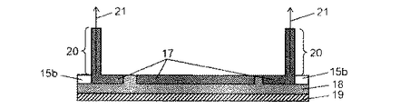
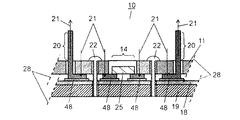
図1は、放熱構造体基板の接続配線部を高強度化するために用いる樹脂構造体の一例を示す斜視図である。図1において、放熱構造体基板10は、樹脂構造体11、取付け孔12、配線孔13、開口部14、凹み部15a、15b、放熱基板16、リードフレーム17、伝熱層18、金属板19、接続配線20、ネジ22で構成されている。   FIG. 1 is a perspective view showing an example of a resin structure used for increasing the strength of a connection wiring portion of a heat dissipation structure substrate. In FIG. 1, the heat dissipation structure substrate 10 includes a resin structure 11, a mounting hole 12, a wiring hole 13, an opening 14, recesses 15 a and 15 b, a heat dissipation substrate 16, a lead frame 17, a heat transfer layer 18, and a metal plate 19. The connection wiring 20 and the screw 22 are included.

なお、樹脂構造体11に設けた配線孔13は、後述する図2等で説明するように、放熱基板16に形成した接続配線20(なお接続配線20は、外部回路等への接続用の端子部としてもよい)が貫通(貫通の代わりに、挿入もしくはガイドもしくは固定されてもよい)される孔に相当する。なお、配線孔13は、用途に応じて溝状としてもよい。なお、溝状とした場合、溝の開口部には、溝にセットした接続配線20が動かないようなガイド機構や接着剤等による固定構造を設けることが望ましい。   Note that the wiring hole 13 provided in the resin structure 11 is a connection wiring 20 formed in the heat dissipation board 16 (note that the connection wiring 20 is a terminal for connection to an external circuit or the like, as will be described later with reference to FIG. 2 and the like. Part may correspond to a hole that penetrates (may be inserted or guided or fixed instead of penetrating). In addition, the wiring hole 13 is good also as groove shape according to a use. In the case of the groove shape, it is desirable to provide a fixing structure with a guide mechanism or an adhesive that prevents the connection wiring 20 set in the groove from moving at the opening of the groove.

図1において、放熱基板16は、金属板19と、この上に形成したシート状の伝熱層18と、この伝熱層18に固定したリードフレーム17と、このリードフレーム17の一部を、伝熱層18や金属板19から略垂直に折り曲げてなる接続配線20から構成している。   In FIG. 1, the heat dissipation substrate 16 includes a metal plate 19, a sheet-like heat transfer layer 18 formed thereon, a lead frame 17 fixed to the heat transfer layer 18, and a part of the lead frame 17. The connecting wire 20 is formed by bending the heat transfer layer 18 and the metal plate 19 substantially vertically.

なお、放熱構造体基板10とは、図1に示すように、放熱基板16と、この放熱基板16の上にネジ22等で固定した樹脂構造体11との合体物とする。これは放熱基板16の一部以上を、その上に固定した樹脂構造体11で固定することで、放熱構造体基板10としての高強度化等の機能が発揮できるためである。   As shown in FIG. 1, the heat dissipation structure substrate 10 is a combination of the heat dissipation substrate 16 and the resin structure 11 fixed on the heat dissipation substrate 16 with screws 22 or the like. This is because by fixing a part or more of the heat dissipation substrate 16 with the resin structure 11 fixed thereon, functions such as an increase in strength as the heat dissipation structure substrate 10 can be exhibited.

なお、この接続配線20を、他のプリント基板や入出力ケーブル等への接続用の端子としてもよい。図1では端子もしくは端子部は図示していない。   The connection wiring 20 may be a terminal for connection to another printed circuit board or an input / output cable. In FIG. 1, the terminals or terminal portions are not shown.

図1に示すように、接続配線20は、金属板19の上に形成したシート状の伝熱層18に固定したリードフレーム17の一部を、略垂直に折り曲げてなる部分である。そして接続配線20の根元部(特に接続配線20の根元部分で、伝熱層18に固定したリードフレーム17部分)は、樹脂構造体11で強固に固定される。なお、このような結合部100とは、ネジ22とネジ22で固定される取付け孔12を組み合わせた構造部をいう。結合部100は、樹脂構造体11の周囲等に、複数個もしくは複数箇所、設けることが望ましい。こうすることで、放熱構造体基板10の更なる高強度化が可能となる。   As shown in FIG. 1, the connection wiring 20 is a portion formed by bending a part of a lead frame 17 fixed to a sheet-like heat transfer layer 18 formed on a metal plate 19 substantially vertically. The base portion of the connection wiring 20 (in particular, the lead frame 17 portion fixed to the heat transfer layer 18 at the base portion of the connection wiring 20) is firmly fixed by the resin structure 11. In addition, such a coupling | bond part 100 means the structure part which combined the attachment hole 12 fixed with the screw 22 and the screw 22. It is desirable to provide a plurality of or a plurality of coupling portions 100 around the resin structure 11 or the like. By doing so, the strength of the heat dissipation structure substrate 10 can be further increased.

図1において、樹脂構造体11は、ネジ22等の物理的固定手段を用いて、放熱基板16の金属板19や、放熱基板16本体を固定する機器のシャーシや筐体(共に図示していない)に物理的に固定し、放熱構造体基板10を構成する。   In FIG. 1, the resin structure 11 is formed by using a physical fixing means such as a screw 22, a metal plate 19 of the heat radiating board 16, and a chassis or casing of a device for fixing the heat radiating board 16 main body (both not shown). ) To form a heat dissipation structure substrate 10.

図1において、接続配線20の一部以上は、必要に応じて樹脂構造体11に形成した配線孔13等を貫通させる構造する。この構造によって、略垂直に折り曲げた接続配線20の補強、曲がり防止、整列等が可能になる。また、樹脂構造体11を用いることで、接続配線20の位置寸法も高精度化できる。また接続配線20を、樹脂構造体11を貫通させることで、互いの接触を防止する効果も得られる。   In FIG. 1, a part or more of the connection wiring 20 has a structure that penetrates the wiring hole 13 or the like formed in the resin structure 11 as necessary. With this structure, the connection wiring 20 bent substantially vertically can be reinforced, prevented from bending, aligned, and the like. Further, by using the resin structure 11, the position dimension of the connection wiring 20 can be increased. Moreover, the effect which prevents a mutual contact is also acquired by making the connection wiring 20 penetrate the resin structure 11. FIG.

図1の凹み部15aは、樹脂構造体11の一部を凹ませた部分であり、樹脂構造体11の一部を凹ませる等によって、接続配線20の根元部分を選択的に押付けている。なお詳細は、後述する図4B等で説明する。   The recessed portion 15a in FIG. 1 is a portion where a part of the resin structure 11 is recessed, and the root portion of the connection wiring 20 is selectively pressed by, for example, denting a part of the resin structure 11. Details will be described later with reference to FIG. 4B and the like.

図1の凹み部15bは、シート状の伝熱層18の一部の凹み部分であり、たとえば伝熱層18に埋め込むように固定したリードフレーム17の一部を剥がし、接続配線20とした痕跡部分である。このようにリードフレーム17の一部を引き剥がすことで、金属板19との間で所定の沿面距離が得られ、1次側回路に対応できる。   The recess 15b in FIG. 1 is a part of the recess of the sheet-like heat transfer layer 18. For example, a trace of the lead wire 17 fixed so as to be embedded in the heat transfer layer 18 is removed to form the connection wiring 20. Part. By peeling off a part of the lead frame 17 in this way, a predetermined creepage distance can be obtained between the metal plate 19 and the primary side circuit.

図1では、リードフレーム17は、伝熱層18にその一部以上を埋め込んでいるが、これは伝熱層18とリードフレーム17との接触面積を増加することで、互いの放熱性や密着性を高めるためである。またリードフレーム17の一部以上を埋め込むことで、リードフレーム17により肉厚の部材を用いても、その厚みが表面に凹凸として表れないため、ソルダーレジスト(図示していない)等の形成が容易となる。   In FIG. 1, a part of the lead frame 17 is embedded in the heat transfer layer 18, but this increases the contact area between the heat transfer layer 18 and the lead frame 17, thereby improving the heat dissipation and adhesion between each other. This is to increase sex. Further, by embedding a part or more of the lead frame 17, even if a thick member is used by the lead frame 17, the thickness does not appear as unevenness on the surface, so that it is easy to form a solder resist (not shown) or the like It becomes.

なお、リードフレーム17は、必ずしも伝熱層18に埋め込む必要はない。シート状やフィルム状の伝熱層18の表面にリードフレーム17を接着剤等で固定してもよい。これはリードフレーム17を接着剤だけで固定した場合であっても、実施の形態1で説明するように、樹脂構造体11がリードフレーム17を伝熱層18側に固定し、放熱構造体基板10を構成するためである。なお、伝熱層18としては、熱硬化樹脂にセラミック粉等を添加したものや、キャスティング法等で作成した高熱伝導性樹脂フィルム(例えば、ポリイミドフィルム等)を用いる。   The lead frame 17 is not necessarily embedded in the heat transfer layer 18. The lead frame 17 may be fixed to the surface of the sheet-like or film-like heat transfer layer 18 with an adhesive or the like. Even if this is the case where the lead frame 17 is fixed only by the adhesive, as described in the first embodiment, the resin structure 11 fixes the lead frame 17 to the heat transfer layer 18 side, and the heat dissipation structure substrate. This is because the number 10 is configured. In addition, as the heat-transfer layer 18, what added ceramic powder etc. to the thermosetting resin, or the highly heat conductive resin film (for example, polyimide film etc.) created by the casting method etc. are used.

図1において、樹脂構造体11は四角形(中央部に開口部14を構成した形状)としているが、直線状のもの、L字型、U字型等、必要に応じた形状とする。   In FIG. 1, the resin structure 11 has a quadrangular shape (a shape in which the opening portion 14 is formed in the central portion). However, the resin structure 11 has a linear shape, an L shape, a U shape, or the like as necessary.

図1において、取付け孔12は、樹脂構造体11の周縁部に形成しているが、周縁部に設けることで、放熱基板16から伸びる接続配線20との干渉を防止する。   In FIG. 1, the attachment hole 12 is formed in the peripheral portion of the resin structure 11. However, the attachment hole 12 prevents interference with the connection wiring 20 extending from the heat dissipation substrate 16 by being provided in the peripheral portion.

次に、図2を用いて、放熱基板16に、樹脂構造体11をセットし、放熱構造体基板10とする様子について説明する。図2は、放熱基板16に、樹脂構造体11をセットする様子を説明する斜視図である。   Next, a state in which the resin structure 11 is set on the heat dissipation substrate 16 to form the heat dissipation structure substrate 10 will be described with reference to FIG. FIG. 2 is a perspective view for explaining how the resin structure 11 is set on the heat dissipation board 16.

なお、図2において、放熱基板16は、金属板19の上に、シート状の伝熱層18を介して、リードフレーム17を固定している。また、図2において、リードフレーム17の一部(例えば放熱基板16の中央部等の、パワー半導体等を実装する回路パターン部分やパワー半導体等)は図示していない。また図2において、リードフレーム17の下部に挿入した伝熱層18も図示していない。またソルダーレジスト等も図示していない。   In FIG. 2, the heat dissipation substrate 16 has a lead frame 17 fixed on a metal plate 19 via a sheet-like heat transfer layer 18. In FIG. 2, a part of the lead frame 17 (for example, a circuit pattern portion on which a power semiconductor or the like is mounted such as a central portion of the heat dissipation substrate 16 or a power semiconductor) is not illustrated. In FIG. 2, the heat transfer layer 18 inserted in the lower part of the lead frame 17 is not shown. Also, solder resist and the like are not shown.

図2において、リードフレーム17は、その一部例えば、放熱基板16の周縁部においては、互いに略平行な状態のまま、金属板19から略垂直になるように折り曲げており、この部分を接続配線20とする。そして図2の矢印21に示すように、放熱基板16に樹脂構造体11を装着し、放熱構造体基板10とする。   In FIG. 2, a part of the lead frame 17, for example, a peripheral portion of the heat dissipation substrate 16 is bent so as to be substantially perpendicular to the metal plate 19 while being substantially parallel to each other. 20 Then, as shown by an arrow 21 in FIG. 2, the resin structure 11 is attached to the heat dissipation board 16 to obtain the heat dissipation structure board 10.

なお、樹脂構造体11には、ネジ22等の結合部100によって、樹脂構造体11を、金属板19もしくは伝熱層18のどちらか一方以上(なお一方以上とは、両方も含む)、もしくは金属板19を固定する機器のシャーシ(なおシャーシは機器筐体等も含む。なおシャーシも筐体も図示していない)の、いずれか一つ以上に固定する結合部100を設けることが望ましい。なお、結合部100とは、例えば図2に示す樹脂構造体11の周縁部等に設けたネジ22とネジ22で固定される取付け孔12を組み合わせた構造部に相当する。   In addition, the resin structure 11 is attached to the resin structure 11 by one or more of the metal plate 19 or the heat transfer layer 18 by the coupling portion 100 such as the screw 22 (note that one or more includes both), or It is desirable to provide a coupling portion 100 for fixing to any one or more of a chassis of a device for fixing the metal plate 19 (note that the chassis includes a device housing and the like, neither the chassis nor the housing is shown). In addition, the coupling | bond part 100 is corresponded to the structure part which combined the attachment hole 12 fixed with the screw | thread 22 provided in the peripheral part etc. of the resin structure 11 shown in FIG.

更に、樹脂構造体11には、リードフレーム17の一部以上と伝熱層18との界面の密着強度,剥離強度,もしくは伝熱層18と金属板19との密着強度、もしくは接続配線20の機械的強度のいずれか一つ以上の強度を高めるようにする、強化部101あるいはガイド部102を設ける。なお、強化部101とは、リ−ドフレ−ム17に樹脂構造体11が圧接する部分であり、ガイド部102とは、図2に示す樹脂構造体11の配線孔13に相当する。このように一つの樹脂構造体11に、結合等に寄与する結合部100と、高強度化等に寄与する強化部101とを、一体化して設けることで、放熱基板16自体のみならず、放熱基板16に固定された樹脂構造体11や、放熱構造体基板10自体も高強度化できる。   Further, the resin structure 11 has adhesion strength, peeling strength at the interface between the part of the lead frame 17 and the heat transfer layer 18, adhesion strength between the heat transfer layer 18 and the metal plate 19, or connection wiring 20. A reinforcing part 101 or a guide part 102 is provided to increase one or more of the mechanical strengths. The reinforcing portion 101 is a portion where the resin structure 11 is in pressure contact with the lead frame 17, and the guide portion 102 corresponds to the wiring hole 13 of the resin structure 11 shown in FIG. As described above, by providing the single resin structure 11 with the coupling portion 100 that contributes to the coupling and the like and the reinforcing portion 101 that contributes to the enhancement of the strength and the like, not only the heat dissipation substrate 16 itself but also the heat dissipation. The strength of the resin structure 11 fixed to the substrate 16 and the heat dissipation structure substrate 10 itself can also be increased.

なお、結合部100と、強化部101あるいはガイド部102は、互いに重複してもよいし、結合部100と、強化部101あるいはガイド部102が組み合わされて一つ以上の樹脂構造体11を構成してもよい。また結合部100と、強化部101あるいはガイド部102が、分割可能である必要はなし。結合部100と、強化部101あるいはガイド部102とを、一つの樹脂構造体11に設けることで、樹脂構造体11の低コスト化や、その取付け工数の削減が可能となる。   In addition, the coupling | bond part 100 and the reinforcement | strengthening part 101 or the guide part 102 may mutually overlap, and the one or more resin structure 11 is comprised by combining the coupling | bond part 100 and the reinforcement | strengthening part 101 or the guide part 102. May be. Further, the coupling part 100 and the reinforcing part 101 or the guide part 102 need not be separable. By providing the coupling part 100 and the reinforcing part 101 or the guide part 102 in one resin structure 11, the cost of the resin structure 11 can be reduced and the number of mounting steps can be reduced.

なお、図2に示すように、接続配線20の先端は、樹脂構造体11等への挿入性を高めるために尖らせておく方がよい。またリードフレーム17等の一部は、省略している。   In addition, as shown in FIG. 2, it is better to sharpen the front-end | tip of the connection wiring 20 in order to improve the insertability to the resin structure 11 grade | etc.,. A part of the lead frame 17 and the like is omitted.

図2に示すように、放熱基板16の周縁部の一部以上に形成したリードフレーム17の一部を金属板19から略垂直に折り曲げてなる接続配線20に、ネジ22等を用いて矢印21に示すように樹脂構造体11を固定する。この結果、放熱基板16におけるリードフレーム17は、ネジ22等によって金属板19に固定した樹脂構造体11によって、保護すると共にその機械的強度を高める。   As shown in FIG. 2, a connection wire 20 formed by bending a part of a lead frame 17 formed at least a part of the peripheral edge of the heat dissipation board 16 from a metal plate 19 substantially vertically is connected to an arrow 21 using a screw 22 or the like. The resin structure 11 is fixed as shown in FIG. As a result, the lead frame 17 in the heat dissipation board 16 is protected and enhanced in mechanical strength by the resin structure 11 fixed to the metal plate 19 with screws 22 or the like.

なお、放熱基板16の周縁部全てに樹脂構造体11を設ける必要はない。放熱基板16の周縁部の一部(あるいは一辺)、あるいは放熱基板16の内部例えば、中央部等、必要な部分に設ければよい。なお、樹脂構造体11の構造は、高強度化を行おうとするリードフレーム17や伝熱層18等を覆うように設計する。これは高強度化を行おうとする部材や部位を覆うように樹脂構造体11を設けることで、樹脂構造体11がこれら部材や部位を構造的に押さえられるからである。   In addition, it is not necessary to provide the resin structure 11 in all the peripheral parts of the thermal radiation board | substrate 16. FIG. What is necessary is just to provide in a part (or one side) of the peripheral part of the thermal radiation board | substrate 16, or a required part, such as a center part inside the thermal radiation board | substrate 16, for example. The structure of the resin structure 11 is designed so as to cover the lead frame 17 and the heat transfer layer 18 and the like to be increased in strength. This is because the resin structure 11 can structurally hold these members and parts by providing the resin structure 11 so as to cover the members and parts to be strengthened.

以上のように、放熱構造体基板10は、金属板19と、この金属板19上に形成したシート状の伝熱層18と、この伝熱層18に固定したリードフレーム17と、リードフレーム17の伝熱層18に固定された一部以上と、重なるように配置された一つ以上の樹脂構造体11とからなる。このリードフレーム17の一部を伝熱層18から突き出して接続配線20とする。樹脂構造体11が、金属板19もしくは伝熱層18のどちらか一方以上、もしくは金属板19を固定する機器のシャーシの、いずれか一つ以上に固定される結合部100と、リードフレーム17の一部以上と伝熱層18との密着強度、もしくは伝熱層18と金属板19との密着強度、もしくは接続配線20の機械的強度、のいずれか一つ以上を高めるガイド部102あるいは強化部101と、を有する樹脂構造体11を放熱構造体基板10の一部として構成する。   As described above, the heat dissipation structure substrate 10 includes the metal plate 19, the sheet-like heat transfer layer 18 formed on the metal plate 19, the lead frame 17 fixed to the heat transfer layer 18, and the lead frame 17. It consists of one or more parts fixed to the heat transfer layer 18 and one or more resin structures 11 arranged so as to overlap. A part of the lead frame 17 protrudes from the heat transfer layer 18 to form a connection wiring 20. The resin structure 11 includes a coupling portion 100 that is fixed to at least one of the metal plate 19 and the heat transfer layer 18, or a chassis of a device that fixes the metal plate 19, and the lead frame 17. A guide portion 102 or a reinforcing portion that increases at least one of the adhesion strength between a part or more and the heat transfer layer 18, the adhesion strength between the heat transfer layer 18 and the metal plate 19, or the mechanical strength of the connection wiring 20. 101 is formed as a part of the heat dissipation structure substrate 10.

そして、結合部100も、樹脂構造体11のリードフレーム17の一部からなる端子部103あるいは接続配線20を保護あるいはガイドするガイド部102(あるいは配線孔13)はリードフレーム17や、水平方向や、任意の角度に突き出してなる接続配線20や端子部等を保護、強化、あるいはガイドする。   In addition, the connecting portion 100 also has a terminal portion 103 or a guide portion 102 (or wiring hole 13) that protects or guides a part of the lead frame 17 of the resin structure 11 as a lead frame 17 or a horizontal direction. The connection wiring 20 protruding at an arbitrary angle, the terminal portion, and the like are protected, strengthened, or guided.

このように、樹脂構造体11を設けない状態で、測定した接続配線20やリードフレーム17の密着強度や機械的強度に比べ、樹脂構造体11を設けることで(更には接続配線20を、金属板19もしくは伝熱層18のどちらか一方以上、もしくは金属板19を固定する機器のシャーシの、いずれか一つ以上に固定した状態で)、これらの密着強度や機械的強度を高められる。なお、密着強度等は、電子部品等の引張り試験等を参考にできる。こうして密着強度や機械的強度を高め、更に耐振性例えば、10G〜30Gの振動試験も高める。   As described above, by providing the resin structure 11 in comparison with the measured adhesion strength and mechanical strength of the connection wiring 20 and the lead frame 17 in a state where the resin structure 11 is not provided (further, the connection wiring 20 is made of metal. The adhesion strength and mechanical strength of the plate 19 and the heat transfer layer 18 can be increased when the metal plate 19 is fixed to at least one of the plates 19 or the heat transfer layer 18. The adhesion strength and the like can be referred to a tensile test of an electronic component or the like. In this way, adhesion strength and mechanical strength are increased, and vibration resistance, for example, vibration tests of 10G to 30G are also enhanced.

なお、図1等に示すように、樹脂構造体11の中央部には開口部14を形成しているが、これは放熱基板16の上に実装した発熱部品(図示していない)の外観検査等に利用できる。   In addition, as shown in FIG. 1 etc., although the opening part 14 is formed in the center part of the resin structure 11, this is the external appearance test | inspection of the heat-emitting component (not shown) mounted on the thermal radiation board | substrate 16. Can be used for etc.

このように樹脂構造体11の周縁部等に、適宜、配線孔13や取付け孔12を形成する。また、配線孔13の外周部(特に、外から見える部分)には、凹み部15aを形成する。この凹み部15aを形成することで、樹脂構造体11と放熱基板16との密着性、あるいは放熱構造体10との密着性を高める。また接続配線20の配線孔13への挿入性を高め効果もある。また放熱基板16に樹脂構造体11を固定し、放熱構造体基板10とした後でも、この凹み部15aによって電気的特性チェックを行える。なお凹み部15aは必要に応じて設ければよい。また凹み部15aを大きくすることで、配線孔13の一側面を開口(あるいは配線孔13)の溝化も可能である。または配線孔13を細長い溝状としてもよい。   In this manner, the wiring hole 13 and the attachment hole 12 are appropriately formed in the peripheral portion of the resin structure 11 or the like. Further, a recess 15a is formed in the outer peripheral portion of the wiring hole 13 (particularly, the portion visible from the outside). By forming the recess 15a, the adhesion between the resin structure 11 and the heat dissipation substrate 16 or the adhesion with the heat dissipation structure 10 is enhanced. In addition, there is an effect of improving the insertion property of the connection wiring 20 into the wiring hole 13. Further, even after the resin structure 11 is fixed to the heat dissipation board 16 to form the heat dissipation structure board 10, the electrical characteristics can be checked by the recess 15a. In addition, what is necessary is just to provide the recessed part 15a as needed. Further, by enlarging the recess 15a, it is possible to form a groove on one side surface of the wiring hole 13 (or the wiring hole 13). Alternatively, the wiring hole 13 may be formed in an elongated groove shape.

なお、配線孔13は、孔形状以外に、溝形状としてもよい。また、配線孔13をガイド部102とすることで、リードフレーム17の一部からなる接続配線20や端子(接続配線20の一部)をガイドし、保護、高強度化できる。なお、配線孔13にテーパー状のガイド機能を有するガイド構造を設け、これをガイド部としてもよい。このようにガイド部102と、配線孔13は同じもの、あるいは互いに一体化したものとしてもよい。   The wiring hole 13 may have a groove shape in addition to the hole shape. Further, by using the wiring hole 13 as the guide portion 102, the connection wiring 20 and the terminal (part of the connection wiring 20) formed of a part of the lead frame 17 can be guided, and protection and strength can be increased. The wiring hole 13 may be provided with a guide structure having a tapered guide function, and this may be used as a guide portion. Thus, the guide part 102 and the wiring hole 13 may be the same or integrated with each other.

また、配線孔13に、接続配線20を挿入することで、接続配線20の一部に曲がりや歪み等が残っていても、接続配線20の曲がりや歪みを矯正する(あるいは調芯する)効果が得られる。その結果、後述する図6で説明するように、プリント基板24に形成した配線孔13への、接続配線20の挿入性を高める。   Further, by inserting the connection wiring 20 into the wiring hole 13, even if bending or distortion or the like remains in a part of the connection wiring 20, the effect of correcting (or aligning) the bending or distortion of the connection wiring 20. Is obtained. As a result, as described later with reference to FIG. 6, the insertion property of the connection wiring 20 into the wiring hole 13 formed in the printed board 24 is improved.

更に、この樹脂構造体11を用いることで、放熱基板16の接続配線20等が強度アップできる分、金属板19の薄層化や軽量化が可能となる。なお、樹脂構造体11は、耐熱性の高い樹脂で作成することで、その熱に対する信頼性を高める。なお樹脂を用いるのは、所定の形状への成形性(射出成形等を含む)や、軽量化のためであり、セラミック等に比べて、樹脂が加工性や材料費の面からも安価であるである。   Furthermore, by using this resin structure 11, the metal plate 19 can be made thinner and lighter because the connection wiring 20 and the like of the heat dissipation board 16 can be strengthened. In addition, the resin structure 11 improves the reliability with respect to the heat | fever by producing with resin with high heat resistance. The resin is used for moldability into a predetermined shape (including injection molding) and weight reduction, and the resin is cheaper in terms of workability and material cost than ceramics. It is.

なお、樹脂構造体11は、射出成型可能な樹脂単体で作成してもよいが、金属部品等と組み合わせてもよい。あるいは樹脂構造体11を射出成型する際に多色成型する。あるいは内部や表面等に金属等の高強度材料と一体化して成型してもよい。こうすることで更に機械的な強度が向上する。また、樹脂構造体11を複数の部品に分けてもよい。こうして一つ以上からなる接続配線20、あるいは複数個の部品が組み合わされてなる樹脂構造体11とすることで、樹脂構造体11の多品種への対応が可能となり、生産コストを抑えられる。   The resin structure 11 may be made of a single injection-moldable resin, but may be combined with a metal part or the like. Alternatively, multicolor molding is performed when the resin structure 11 is injection molded. Alternatively, it may be molded integrally with a high-strength material such as metal inside or on the surface. By doing so, the mechanical strength is further improved. Further, the resin structure 11 may be divided into a plurality of parts. Thus, by using the connection structure 20 composed of one or more or the resin structure 11 formed by combining a plurality of components, it is possible to deal with a wide variety of resin structures 11 and to reduce the production cost.

更に、樹脂構造体11の放熱基板16への取り付け方や固定方法を工夫することで、放熱基板16や放熱構造体基板10におけるリードフレーム17の引張り強度以外に、押し付け強度や捻り強度、あるいは耐振動性等における高強度化(あるいは補強)が可能となる。またこの補強効果の分だけ、伝熱層18における無機フィラー等の充填率を高め、放熱基板16の放熱性を改善できる。これは伝熱層18における無機フィラーの充填率を増加させるほど、伝熱層18における樹脂成分の充填率が低下し、伝熱層18とリードフレーム17との接着力が低下する可能性があるためである。   Furthermore, by devising how to attach and fix the resin structure 11 to the heat dissipation board 16, in addition to the tensile strength of the lead frame 17 in the heat dissipation board 16 or the heat dissipation structure board 10, the pressing strength, the twist strength, or the resistance It is possible to increase the strength (or to reinforce) the vibration characteristics. In addition, the filling rate of the inorganic filler or the like in the heat transfer layer 18 can be increased by the amount of this reinforcing effect, and the heat dissipation of the heat dissipation substrate 16 can be improved. As the filling rate of the inorganic filler in the heat transfer layer 18 increases, the filling rate of the resin component in the heat transfer layer 18 decreases, and the adhesive force between the heat transfer layer 18 and the lead frame 17 may decrease. Because.

なお樹脂構造体11による押付け部分の構造や取り付け方等は、その用途に応じて最適な形状に設計する。   In addition, the structure of the pressing part by the resin structure 11 and how to attach the resin structure 11 are designed in an optimum shape according to the application.

なお、金属板19と、この金属板19上に設けられた伝熱層18と、端子部103とを有し、この端子部103を除く部分が伝熱層18に固着されたリードフレーム17と、このリードフレーム17の端子部を除く部分の上面に結合された樹脂製の構造体11と、からなる放熱構造体基板10であって、樹脂製の構造体11が、金属板19または金属板19が結合された部材と結合するための結合部100と、リードフレーム17に設けられた端子部103をガイドするガイド部102(例えば、図2における配線孔13等)と、を有するものである放熱構造体基板10としてもよい。なお、接続配線20は、端子部103の一部である。接続配線20も端子部103も、使用用途等によって使い分けできるからである。樹脂構造体11が、端子部103や接続配線20のいずれか一つ以上をガイドすることで、これらを高強度化できると共に、挿入等の作業性を改善する。   The lead frame 17 includes a metal plate 19, a heat transfer layer 18 provided on the metal plate 19, and a terminal portion 103, and a portion excluding the terminal portion 103 is fixed to the heat transfer layer 18. The heat dissipating structure substrate 10 is composed of a resin structure 11 coupled to the upper surface of the lead frame 17 excluding the terminal portion, and the resin structure 11 is a metal plate 19 or a metal plate. And a guide portion 102 (for example, the wiring hole 13 in FIG. 2) for guiding the terminal portion 103 provided in the lead frame 17. The heat dissipation structure substrate 10 may be used. Note that the connection wiring 20 is a part of the terminal portion 103. This is because both the connection wiring 20 and the terminal portion 103 can be used properly depending on the intended use. The resin structure 11 guides any one or more of the terminal portion 103 and the connection wiring 20, so that these can be strengthened and workability such as insertion can be improved.

なお、接続配線20を、伝熱層18に固定したリードフレーム17と、重なるように配置することで、樹脂構造体11によって、接続配線20を直接、伝熱層18側に押し付けることができ、接続配線20(あるいは端子部103)等の高強度化が可能となる。   In addition, by arranging the connection wiring 20 so as to overlap the lead frame 17 fixed to the heat transfer layer 18, the connection wiring 20 can be pressed directly to the heat transfer layer 18 side by the resin structure 11. The strength of the connection wiring 20 (or the terminal portion 103) or the like can be increased.

また、樹脂構造体11が、金属板19もしくは伝熱層18のどちらか一方以上、もしくは金属板19を固定する機器のシャーシの、いずれか一つ以上に固定される結合部100(例えば、図1の取付け孔12)と、リードフレーム17の一部以上と伝熱層18との密着強度、もしくは伝熱層18と金属板19との密着強度、もしくは接続配線20の機械的強度、のいずれか一つ以上を高める強化部101と、を設けることで、放熱基板16や放熱構造体基板10全体のみならず、接続配線20(あるいはリードフレーム17の一部からなる端子部103)等の高強度化が可能となる。   In addition, the coupling portion 100 (for example, the figure) in which the resin structure 11 is fixed to any one or more of the metal plate 19 and the heat transfer layer 18 or the chassis of the device that fixes the metal plate 19. 1, the adhesion strength between one or more of the lead frames 17 and the heat transfer layer 18, the adhesion strength between the heat transfer layer 18 and the metal plate 19, or the mechanical strength of the connection wiring 20. By providing the strengthening portion 101 that enhances one or more, not only the heat dissipation substrate 16 and the entire heat dissipation structure substrate 10, but also the connection wiring 20 (or the terminal portion 103 formed of a part of the lead frame 17) and the like are high. Strengthening is possible.

このように、樹脂構造体11によって、リードフレーム17の一部以上と伝熱層18との密着強度、もしくは伝熱層18と金属板19との密着強度、もしくは接続配線20の機械的強度、のいずれか一つ以上を高めることができる。こうした強化部101は、例えば、図1の接続配線20に形成した凹み部15bに相当する。これは樹脂構造体11に設けた凹み部15aが、リードフレーム17を伝熱層18側に押し付けるように固定するためである。   Thus, by the resin structure 11, the adhesion strength between a part of the lead frame 17 and the heat transfer layer 18, the adhesion strength between the heat transfer layer 18 and the metal plate 19, or the mechanical strength of the connection wiring 20, Any one or more of these can be raised. Such a reinforced portion 101 corresponds to, for example, the recessed portion 15b formed in the connection wiring 20 of FIG. This is because the recess 15a provided in the resin structure 11 fixes the lead frame 17 so as to press it against the heat transfer layer 18 side.

このように、樹脂構造体11の結合部100と、強化部101を、共に一つの接続配線20の一部分とすることで、これら各部位の機械的な結合強度を高められる。   As described above, the joint portion 100 and the reinforcing portion 101 of the resin structure 11 are both part of one connection wiring 20, so that the mechanical joint strength of these portions can be increased.

なお、図1において、接続配線20や端子部103等のいずれか一つ以上(あるいは一部以上)は、放熱基板16や伝熱層18の周縁部(あるいは周縁部の一部)に形成しており、接続配線20(あるいは端子部)は、伝熱層18から略垂直に折り曲げているが、これは例えば、金属板19と、接続配線20との間の沿面距離を確保するために有用である。   In FIG. 1, one or more (or a part or more) of the connection wiring 20, the terminal part 103, or the like is formed on the peripheral part (or part of the peripheral part) of the heat dissipation substrate 16 or the heat transfer layer 18. The connection wiring 20 (or the terminal portion) is bent substantially perpendicularly from the heat transfer layer 18, which is useful for securing a creeping distance between the metal plate 19 and the connection wiring 20, for example. It is.

放熱基板16と、樹脂構造体11とは、一体物とする必要はない。これら部材を別々に用意することで、放熱基板16や放熱構造体基板10に、パワー半導体等の放熱が必要な電子部品を半田付け等で実装した後、取り付けられる。このように樹脂構造体11は、放熱基板16や放熱構造体基板10に後付けできる構造とする。こうすることで、接続配線20が半田付け等の熱影響を受けることなく、パワー半導体等の半田付け作業時に樹脂構造体11が邪魔になることもない。また、接続配線20と、放熱基板16や放熱構造体基板10とを、接着剤等で固定してもよいが、ネジ22のような取り外し可能な状態で固定してもよい。取り外し可能な状態で固定することで、メンテナンス等の作業性を高められる。   The heat dissipation board 16 and the resin structure 11 do not need to be integrated. By preparing these members separately, an electronic component such as a power semiconductor that requires heat dissipation is mounted on the heat dissipation substrate 16 or the heat dissipation structure substrate 10 by soldering or the like and then attached. Thus, the resin structure 11 has a structure that can be retrofitted to the heat dissipation substrate 16 or the heat dissipation structure substrate 10. By doing so, the connection wiring 20 is not affected by heat such as soldering, and the resin structure 11 does not get in the way during soldering work of a power semiconductor or the like. Further, the connection wiring 20 and the heat dissipation substrate 16 or the heat dissipation structure substrate 10 may be fixed with an adhesive or the like, but may be fixed in a detachable state such as a screw 22. By fixing in a detachable state, workability such as maintenance can be improved.

(実施の形態2)
次に実施の形態2として、図3A,図3Bから図4A,図4Bを用いて、実施の形態1で説明した放熱基板16や放熱構造体基板10の製造方法の一例について説明する。
(Embodiment 2)
Next, as a second embodiment, an example of a method for manufacturing the heat dissipation substrate 16 and the heat dissipation structure substrate 10 described in the first embodiment will be described with reference to FIGS. 3A and 3B to FIGS. 4A and 4B.

図3A、図3Bは、共に放熱基板16の製造方法の一例を説明する断面図である。   3A and 3B are cross-sectional views illustrating an example of a method for manufacturing the heat dissipation substrate 16.

まず、図3Aに示すように、金属板19の上に、伝熱樹脂23をセットし、更にその上に所定パターン形状に加工したリードフレーム17をセットする。そして矢印21に示すように、これらを金型やプレス(共に図示していない)を用いて、加熱加圧することで一体化する。そして伝熱樹脂23を硬化し、伝熱層18とする。   First, as shown in FIG. 3A, the heat transfer resin 23 is set on the metal plate 19, and the lead frame 17 processed into a predetermined pattern shape is further set thereon. And as shown by the arrow 21, these are integrated by heat-pressing using a metal mold | die and a press (both are not shown in figure). Then, the heat transfer resin 23 is cured to form the heat transfer layer 18.

図3Bは、伝熱樹脂23を硬化し、伝熱層18とした後の状態を示す断面図である。図3Bに示すように、放熱基板16を構成するリードフレーム17は、その一部以上を伝熱層18に埋め込んでいる。こうすることで、リードフレーム17と伝熱層18との接触面積を増加させ、リードフレーム17に実装したパワー半導体(図示していない)の熱を、リードフレーム17から伝熱層18を介して金属板19へ放熱する。またリードフレーム17と伝熱層18との接合強度(あるいは剥離強度)を高める。   FIG. 3B is a cross-sectional view showing a state after the heat transfer resin 23 is cured to form the heat transfer layer 18. As shown in FIG. 3B, a part of the lead frame 17 constituting the heat dissipation substrate 16 is embedded in the heat transfer layer 18. By doing so, the contact area between the lead frame 17 and the heat transfer layer 18 is increased, and the heat of the power semiconductor (not shown) mounted on the lead frame 17 is transferred from the lead frame 17 through the heat transfer layer 18. Heat is radiated to the metal plate 19. Further, the bonding strength (or peel strength) between the lead frame 17 and the heat transfer layer 18 is increased.

次に、図3Bの矢印21で示すように、リードフレーム17の一部を、金属板19等より略垂直に折曲げ、図4Aの形状とする。   Next, as indicated by an arrow 21 in FIG. 3B, a part of the lead frame 17 is bent substantially perpendicularly from the metal plate 19 or the like to obtain the shape of FIG. 4A.

図4A、図4Bは、共に接続配線20部分を強化した放熱基板16の製造方法の一例を説明する断面図である。   4A and 4B are cross-sectional views illustrating an example of a method for manufacturing the heat dissipation board 16 in which the connection wiring 20 portion is reinforced.

図4Aにおいて、伝熱層18に埋め込んだリードフレーム17の一部を引き起こし(あるいは引き剥がし)、接続配線20あるいは端子部(図示していない)としている。ここで伝熱層18から引き剥がした部分を、凹み部15bとすることで、金属板19と接続配線20との間の沿面距離とすることで、絶縁性を高める。なお図4A、図4Bでは、引き剥がした部分を略垂直に折曲げ、接続配線20としているが、用途に応じて曲げる角度(あるいは曲げる曲げない)を選択する。   In FIG. 4A, a part of the lead frame 17 embedded in the heat transfer layer 18 is caused (or peeled off) to be a connection wiring 20 or a terminal portion (not shown). Here, the portion peeled off from the heat transfer layer 18 is used as a recess 15b, so that the creeping distance between the metal plate 19 and the connection wiring 20 is increased, thereby improving the insulation. In FIG. 4A and FIG. 4B, the peeled portion is bent substantially vertically to form the connection wiring 20, but an angle to be bent (or not bent) is selected according to the application.

次に図4Bに示すように、放熱基板16の上に、樹脂構造体11をセットし、ネジ22を用いて、矢印21に示すようにこれらを固定し、これを放熱構造体基板10とする。なお、図4Bにおいて、ネジ22は、接続配線20の後ろ側に図示している。これは金属製のネジ22と、接続配線20とがショートしないためである。なおネジ22は金属等の高強度で伝熱性に優れたものを用いることが望ましい。また、高強度が必要な場合、M3以上、更にはM4以上、あるいはM6以上の太いものを用いる。なおM3等はJISによるネジ22の規格である。   Next, as shown in FIG. 4B, the resin structure 11 is set on the heat dissipation substrate 16, and these are fixed as shown by an arrow 21 using screws 22, and this is used as the heat dissipation structure substrate 10. . In FIG. 4B, the screw 22 is illustrated on the rear side of the connection wiring 20. This is because the metal screw 22 and the connection wiring 20 do not short-circuit. The screw 22 is preferably made of metal or the like having high strength and excellent heat conductivity. Further, when high strength is required, a thick material of M3 or more, further M4 or more, or M6 or more is used. M3 and the like are standards for the screw 22 according to JIS.

図4Bに示すように、樹脂構造体11の一部(例えば、外周面の一部、あるいは外周面の放熱基板16に接する部分)に凹み部15a、15bを形成しておくことで、例えばリードフレーム17が、樹脂構造体11に形成した配線孔13に挿入できたかどうかの確認が容易になる。また樹脂構造体11とリードフレーム17との密着性を高められる。   As shown in FIG. 4B, by forming recesses 15a and 15b in a part of the resin structure 11 (for example, a part of the outer peripheral surface or a part of the outer peripheral surface in contact with the heat dissipation substrate 16), for example, leads It is easy to confirm whether or not the frame 17 has been inserted into the wiring hole 13 formed in the resin structure 11. Further, the adhesion between the resin structure 11 and the lead frame 17 can be improved.

次に放熱基板16(あるいは放熱構造体基板10)の接続配線20部分等の高強化について説明する。図4Bに示すように、例えば、放熱基板16の接続配線20の根元を樹脂構造体11で強固に固定することで、接続配線20の高強度化が可能となる。なお根元とは、根元付近も含む。根元付近とは接続配線20の折り曲げした位置(あるいは樹脂構造体11で高強度化したい場所)から半径10mm以下とする。折り曲げした位置や高強度化したい場所から、半径10mmより遠く離れた位置を樹脂構造体11で押し付けても、所定の高強度化効果が得られない場合がある。   Next, high strengthening of the connection wiring 20 portion of the heat dissipation substrate 16 (or the heat dissipation structure substrate 10) will be described. As shown in FIG. 4B, for example, the strength of the connection wiring 20 can be increased by firmly fixing the base of the connection wiring 20 of the heat dissipation board 16 with the resin structure 11. The root includes the vicinity of the root. The vicinity of the root is defined as a radius of 10 mm or less from a position where the connection wiring 20 is bent (or a place where the resin structure 11 is desired to have high strength). Even if the resin structure 11 is pressed at a position far from the radius of 10 mm from the bent position or a place where the strength is desired to be increased, a predetermined effect of increasing the strength may not be obtained.

図4Bに示すように、放熱基板16に形成した接続配線20は、樹脂構造体11に嵌め込む。そしてネジ22等を用いて、樹脂構造体11を放熱基板16の金属板19等に機械的に固定し、放熱構造体基板10とする。図4Bにおける矢印21aは、ネジ22や樹脂構造体11によって発生する「押付け力」を示す。また、矢印21bは、接続配線20に外部等から加えられる外力を示す。例えば、矢印21bで示すような外力例えば、矢印21bに示すような引張り力が発生した場合でも、矢印21aに示す押付け力で打ち消せる。その結果、接続配線20の根元における、リードフレーム17と伝熱層18の界面あるいは伝熱層18と金属板19の界面あるいはその両方の界面に外力(例えば、引っ張り力等)が伝わらないため、剥離例えば、リードフレーム17と伝熱層18との界面での剥離の発生を防止する。   As shown in FIG. 4B, the connection wiring 20 formed on the heat dissipation board 16 is fitted into the resin structure 11. Then, the resin structure 11 is mechanically fixed to the metal plate 19 or the like of the heat dissipation board 16 using screws 22 or the like to obtain the heat dissipation structure board 10. An arrow 21 a in FIG. 4B indicates a “pressing force” generated by the screw 22 or the resin structure 11. An arrow 21b indicates an external force applied to the connection wiring 20 from the outside. For example, even when an external force as indicated by an arrow 21b, for example, a tensile force as indicated by an arrow 21b, is generated, it can be canceled by the pressing force indicated by the arrow 21a. As a result, external force (for example, tensile force) is not transmitted to the interface between the lead frame 17 and the heat transfer layer 18 or the interface between the heat transfer layer 18 and the metal plate 19 or both of the interfaces at the base of the connection wiring 20. Peeling For example, the occurrence of peeling at the interface between the lead frame 17 and the heat transfer layer 18 is prevented.

なお、図4A等における凹み部15aは、樹脂構造体11に形成した配線孔13の一側面以上を開口したもしくは凹ませたものである。このように樹脂構造体11の一部に、凹み部15aを形成することで、樹脂構造体11とリードフレーム17との固定強度を高められる。これは放熱基板16や樹脂構造体11等に反りやうねりが発生しても、凹み部15aを設けることで、凹み部15aや凹み部15bを設けていない側つまりリードフレーム17側で、確実に樹脂構造体11とリードフレーム17側が接するためである。   4A or the like is formed by opening or denting one or more side surfaces of the wiring hole 13 formed in the resin structure 11. Thus, by forming the recess 15a in a part of the resin structure 11, the fixing strength between the resin structure 11 and the lead frame 17 can be increased. Even if warpage or undulation occurs in the heat dissipation substrate 16 or the resin structure 11, etc., by providing the recess 15a, the side where the recess 15a or the recess 15b is not provided, that is, on the lead frame 17 side, can be ensured. This is because the resin structure 11 is in contact with the lead frame 17 side.

次に、図5A、図5Bを用いて、接続配線20の根元付近におけるあるいはリードフレーム17と伝熱層18との間の界面剥離について説明する。図5A、図5Bは、共に樹脂構造体11を設けていない場合における放熱基板16や放熱構造体基板10の接続配線20の根元における界面剥離について説明する断面図である。   Next, with reference to FIGS. 5A and 5B, interface peeling near the root of the connection wiring 20 or between the lead frame 17 and the heat transfer layer 18 will be described. 5A and 5B are cross-sectional views for explaining the interface peeling at the base of the connection wiring 20 of the heat dissipation substrate 16 and the heat dissipation structure substrate 10 when the resin structure 11 is not provided.

図5Aは、放熱基板16や放熱構造体基板10の接続配線20に、矢印21に示す方向に引張り力を発生させた場合について説明する断面図である。   FIG. 5A is a cross-sectional view illustrating a case where a tensile force is generated in the direction indicated by the arrow 21 on the connection wiring 20 of the heat dissipation substrate 16 or the heat dissipation structure substrate 10.

図5Bは、引張り力によって、接続配線20が放熱基板16から引き剥がされた様子を説明する断面図である。振動試験等で非常に大きな引張り力が発生した場合、図5Bに示すようにリードフレーム17と、伝熱層18との界面で剥離する可能性が考えられる。   FIG. 5B is a cross-sectional view illustrating a state in which the connection wiring 20 is peeled off from the heat dissipation substrate 16 by a tensile force. When a very large tensile force is generated in a vibration test or the like, there is a possibility of peeling at the interface between the lead frame 17 and the heat transfer layer 18 as shown in FIG. 5B.

一方、本発明の放熱構造体基板10の場合、図4B等に示すように、放熱基板16の一部を、樹脂構造体11で、補強、固定することで放熱構造体基板10を構成する構成である。そしてこの構造によって、外力がリードフレーム17と伝熱層18等の界面に伝わらないため、これら界面での剥離を防止する。このように樹脂構造体11を、ネジ22等で金属板19等に固定することによって、リードフレームの一部以上と伝熱層18との密着強度、もしくは伝熱層18と金属板19との密着強度、もしくは接続配線20の機械的強度等、のいずれか一つ以上の強度を高める。   On the other hand, in the case of the heat dissipation structure substrate 10 of the present invention, as shown in FIG. 4B and the like, the heat dissipation structure substrate 10 is configured by reinforcing and fixing a part of the heat dissipation substrate 16 with the resin structure 11. It is. With this structure, external force is not transmitted to the interface between the lead frame 17 and the heat transfer layer 18 and the like, and peeling at these interfaces is prevented. In this way, by fixing the resin structure 11 to the metal plate 19 or the like with the screw 22 or the like, the adhesion strength between a part of the lead frame and the heat transfer layer 18 or the heat transfer layer 18 and the metal plate 19 is fixed. One or more strengths such as the adhesion strength or the mechanical strength of the connection wiring 20 are increased.

以上のように、金属板19と、この金属板19上に形成したシート状の伝熱層18と、この伝熱層18に固定したリードフレーム17と、リードフレーム17の伝熱層18に固定された一部以上と、重なるように配置された一つ以上の樹脂構造体11と、からなる放熱構造体基板10の製造方法であって、このリードフレーム17の一部を伝熱層18から突き出して、あるいは略垂直に折り曲げて接続配線20または端子部とするステップと、樹脂構造体11を、前記金属板19もしくは伝熱層18のどちらか一方以上、もしくは金属板19を固定する機器のシャーシ、もしくは金属板19が結合された部材の、いずれか一つ以上に固定するステップと、を有する放熱構造体基板10の製造方法によって、リードフレーム17やリードフレーム17と伝熱層18等の界面部分等の高強度化が可能な放熱構造体基板10を製造する。   As described above, the metal plate 19, the sheet-like heat transfer layer 18 formed on the metal plate 19, the lead frame 17 fixed to the heat transfer layer 18, and the heat transfer layer 18 of the lead frame 17 are fixed. A method of manufacturing a heat dissipation structure substrate 10 comprising a part of the lead frame 17 and one or more resin structures 11 arranged so as to overlap with each other. A step of protruding or bending substantially vertically to form a connection wiring 20 or a terminal portion; and a resin structure 11 that is at least one of the metal plate 19 and the heat transfer layer 18 or a device for fixing the metal plate 19 A step of fixing to one or more of the chassis or the member to which the metal plate 19 is coupled, and the method of manufacturing the heat dissipation structure substrate 10, the lead frame 17 and the lead frame High strength such as a surface portion, such as 17 and the heat transfer layer 18 to produce a heat dissipation structure board 10 as possible.

(実施の形態3)
次に実施の形態3として、放熱基板16や放熱構造体基板10等に用いる部材について説明する。
(Embodiment 3)
Next, as Embodiment 3, members used for the heat dissipation substrate 16, the heat dissipation structure substrate 10, and the like will be described.

リードフレーム17としては、銅やアルミニウムのような熱伝導性の高い部材を用いることが望ましい。またリードフレーム17の厚みは0.2mm以上(望ましくは0.3mm以上)が望ましい。リードフレーム17の厚みが0.2mm未満の場合、接続配線20の強度が低下し、作業中に曲がったり変形したりする可能性がある。   As the lead frame 17, it is desirable to use a member having high thermal conductivity such as copper or aluminum. The thickness of the lead frame 17 is desirably 0.2 mm or more (preferably 0.3 mm or more). When the thickness of the lead frame 17 is less than 0.2 mm, the strength of the connection wiring 20 is lowered, and there is a possibility that the lead frame 17 is bent or deformed during work.

また、リードフレーム17の厚みは、10.0mm以下(望ましくは5.0mm以下)が望ましい。リードフレーム17の厚みが10.0mmを超えた場合、接続配線20のファインパターン化に影響を与える可能性がある。   Further, the thickness of the lead frame 17 is desirably 10.0 mm or less (preferably 5.0 mm or less). When the thickness of the lead frame 17 exceeds 10.0 mm, there is a possibility of affecting the fine patterning of the connection wiring 20.

なお、リードフレーム17の一部以上を、伝熱層18に埋め込むことで、肉厚の(例えば、0.2mm以上、望ましくは0.3mm以上)リードフレーム17を用いた場合でも、その厚みが放熱基板16の表面に段差として表れないため、リードフレーム17の上へのソルダーレジスト(図示していない)の印刷性を高めることができる。   In addition, even when a thick lead frame 17 (for example, 0.2 mm or more, desirably 0.3 mm or more) is used by embedding a part or more of the lead frame 17 in the heat transfer layer 18, the thickness can be reduced. Since it does not appear as a step on the surface of the heat dissipation substrate 16, the printability of a solder resist (not shown) on the lead frame 17 can be improved.

次に伝熱樹脂23について説明する。伝熱樹脂23は、例えば、樹脂とフィラーとからなるものとすることで、その熱伝導性を高めることができる。そして樹脂として熱硬化性の樹脂を用いることで、その信頼性を高めることができる。   Next, the heat transfer resin 23 will be described. The heat transfer resin 23 is made of, for example, a resin and a filler, whereby the thermal conductivity can be increased. And the reliability can be improved by using a thermosetting resin as resin.

ここで無機フィラーとしては、例えば略球形状で、その直径は0.1ミクロン以上100ミクロン以下が適当である。0.1ミクロン未満の場合、樹脂への分散が難しくなる。また、100ミクロンを超えると伝熱層18の厚みが厚くなり熱拡散性に影響を与える。実施の形態3では、無機フィラーに、平均粒径3ミクロンと平均粒径12ミクロンの2種類のアルミナを混合したものを用いている。この大小2種類の粒径のアルミナを用いることによって、大きな粒径のアルミナの隙間に小さな粒径のアルミナを充填できるので、アルミナを90重量%近くまで高濃度に充填できるものである。この結果、これら伝熱層18の熱伝導率は5W/(m・K)程度となる。   Here, as the inorganic filler, for example, a substantially spherical shape and a diameter of 0.1 to 100 microns are appropriate. When it is less than 0.1 micron, dispersion into the resin becomes difficult. On the other hand, if it exceeds 100 microns, the thickness of the heat transfer layer 18 is increased, which affects the thermal diffusibility. In Embodiment 3, a mixture of inorganic fillers with two types of alumina having an average particle size of 3 microns and an average particle size of 12 microns is used. By using alumina having two kinds of large and small particle diameters, it is possible to fill the gaps between the large particle diameters of alumina with small particle diameters, so that alumina can be filled at a high concentration to nearly 90% by weight. As a result, the heat conductivity of these heat transfer layers 18 is about 5 W / (m · K).

なお、無機フィラーとしてはアルミナ、酸化マグネシウム、窒化ホウ素、酸化ケイ素、炭化ケイ素、窒化ケイ素、及び窒化アルミニウム、酸化亜鉛、シリカ、酸化チタン、酸化錫、ジルコン珪酸塩から選択される少なくとも一種以上を含んでいるものとすることが、熱伝導性やコスト面から望ましい。   The inorganic filler includes at least one selected from alumina, magnesium oxide, boron nitride, silicon oxide, silicon carbide, silicon nitride, and aluminum nitride, zinc oxide, silica, titanium oxide, tin oxide, and zircon silicate. It is desirable from the viewpoint of thermal conductivity and cost.

なお、熱硬化性樹脂を使う場合は、エポキシ樹脂、フェノール樹脂、シアネート樹脂、ポリイミド樹脂、アラミド樹脂、PEEK樹脂の群から選ばれた少なくとも1種類の熱硬化性樹脂を含んでいるものが望ましい。これはこれらの樹脂が耐熱性や電気絶縁性に優れているからである。   In addition, when using a thermosetting resin, what contains at least 1 type of thermosetting resin chosen from the group of an epoxy resin, a phenol resin, cyanate resin, a polyimide resin, an aramid resin, and PEEK resin is desirable. This is because these resins are excellent in heat resistance and electrical insulation.

一方、伝熱層18の放熱性を更に高めるには、無機フィラーの含有率を増加させることが必要となるが、この結果、伝熱層18における熱硬化性樹脂の含有率を減らす可能性がある。そして伝熱層18における熱硬化性樹脂の含有率を減らした場合、伝熱層18と、リードフレーム17との間の接着力が低下する可能性がある。その結果、放熱基板16における伝熱層18とリードフレーム17の界面が剥離してしまう可能性が考えられる。   On the other hand, in order to further improve the heat dissipation of the heat transfer layer 18, it is necessary to increase the content of the inorganic filler. As a result, the content of the thermosetting resin in the heat transfer layer 18 may be reduced. is there. And when the content rate of the thermosetting resin in the heat-transfer layer 18 is reduced, the adhesive force between the heat-transfer layer 18 and the lead frame 17 may fall. As a result, there is a possibility that the interface between the heat transfer layer 18 and the lead frame 17 in the heat dissipation substrate 16 may be peeled off.

しかし、本発明では、図4B等に示すように、リードフレーム17特に、接続配線20の根元付近のリードフレーム17等を、樹脂構造体11によって伝熱層18側に物理的に押し付けるような構造とすることで、その部分の物理的強度を高められ、放熱基板16や放熱構造体基板10における伝熱層18とリードフレーム17との界面等の剥離を防止できる。   However, in the present invention, as shown in FIG. 4B and the like, the lead frame 17, in particular, the lead frame 17 near the base of the connection wiring 20 is physically pressed against the heat transfer layer 18 side by the resin structure 11. By doing so, the physical strength of the portion can be increased, and peeling of the interface between the heat transfer layer 18 and the lead frame 17 in the heat dissipation substrate 16 or the heat dissipation structure substrate 10 can be prevented.

(実施の形態4)
次に実施の形態4として、実施の形態1で説明した放熱基板16あるいは放熱構造体基板10に、プリント基板を組合せて、モジュールとした場合について説明する。
(Embodiment 4)
Next, as a fourth embodiment, a case will be described in which a printed board is combined with the heat dissipation board 16 or the heat dissipation structure board 10 described in the first embodiment to form a module.

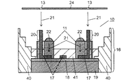
図6は、樹脂構造体11で補強した放熱基板16の上に、プリント基板を固定する様子を説明する斜視図である。   FIG. 6 is a perspective view for explaining how the printed circuit board is fixed on the heat dissipation substrate 16 reinforced with the resin structure 11.

図6において、放熱基板16に形成した接続配線20は、その根元や周辺等を樹脂構造体11で保護している。そして樹脂構造体11は、ネジ22等によって、金属板19やその下の筐体等に固定している。また、矢印21は、接続配線20に、プリント基板24に形成した配線孔13をセットし、モジュール26とする。   In FIG. 6, the connection wiring 20 formed on the heat radiating substrate 16 protects the base and the periphery thereof with the resin structure 11. The resin structure 11 is fixed to the metal plate 19 and the casing below it by screws 22 or the like. In addition, an arrow 21 sets the wiring hole 13 formed in the printed circuit board 24 to the connection wiring 20 and forms a module 26.

こうして金属板19と、この上に形成したシート状の伝熱層18と、この伝熱層18に固定したリードフレーム17と、このリードフレーム17の一部を前記伝熱層18から略垂直に折り曲げてなる接続配線20と、この接続配線20の一部以上を固定する樹脂構造体11と、からなる放熱基板16部分と、プリント基板24部分とから構成される。接続配線20の根元部の一部以上が、樹脂構造体11によって伝熱層18に押付けられ、接続配線20の先端部(先端部は、接続配線20の中央部から上の部分を言う。接続配線20の中央部から下の部分は、接続配線20の根元を構成する一部分となる)の一部以上が、プリント基板24部分に接続しているモジュール26を作成する。   Thus, the metal plate 19, the sheet-like heat transfer layer 18 formed thereon, the lead frame 17 fixed to the heat transfer layer 18, and a part of the lead frame 17 are substantially perpendicular to the heat transfer layer 18. It is composed of a connecting wiring 20 formed by bending, a resin structure 11 for fixing a part or more of the connecting wiring 20, a heat dissipation board 16 part, and a printed board 24 part. A part or more of the base portion of the connection wiring 20 is pressed against the heat transfer layer 18 by the resin structure 11, and the front end portion of the connection wiring 20 (the front end portion is a portion above the center portion of the connection wiring 20. A module 26 in which a part or more of the lower part from the center part of the wiring 20 is a part constituting the base of the connection wiring 20 is connected to the printed circuit board 24 part is created.

なお、図6において、プリント基板24は、1枚以上とする。例えば、複数枚のプリント基板24を、一定距離離しながら、共通する接続配線20で接続、積層してもよい。このように複数枚のプリント基板24同士を、リードフレーム17の一部からなる接続配線20で接続することで、プリント基板24同士を最短で結び、ノイズ発生を低減する。またプリント基板24の固定強度を高めることができる。   In FIG. 6, the number of printed circuit boards 24 is one or more. For example, a plurality of printed circuit boards 24 may be connected and stacked with a common connection wiring 20 while being separated by a certain distance. In this way, by connecting the plurality of printed circuit boards 24 with the connection wiring 20 formed of a part of the lead frame 17, the printed circuit boards 24 are connected in the shortest time, and noise generation is reduced. Further, the fixing strength of the printed circuit board 24 can be increased.

そしてパワートランジスタやパワー半導体等の100Aを超える大電流を取り扱うため発熱を伴うパワー素子(なおパワーFETやパワートランジスタ等のパワー素子は図7には図示していない)は、放熱基板16側例えば、リードフレーム17の表面に固定する。またパワー素子等を制御する一般電子部品25等はプリント基板24側に固定する。そして放熱基板16と、プリント基板24とを、上下方向(あるいは垂直方向、厚み方向)に複数枚に接続する。そしてこの上下方向の接続を、放熱基板16の配線パターンであるリードフレーム17を略垂直に折り曲げてなる接続配線20で行うことで、互いの回路間の引き回し長さ(線路長)を短くできるため、出来上がった回路の耐ノイズ特性を高める。これは線路長を短くした分、接続配線20等が外来ノイズを拾うアンテナとなりにくいためである。   A power element that generates heat in order to handle a large current exceeding 100 A such as a power transistor or a power semiconductor (note that power elements such as a power FET and a power transistor are not shown in FIG. 7) Fix to the surface of the lead frame 17. Further, the general electronic component 25 and the like for controlling the power element and the like are fixed to the printed circuit board 24 side. The heat dissipation board 16 and the printed board 24 are connected to a plurality of sheets in the vertical direction (or the vertical direction and the thickness direction). And since the connection in the vertical direction is made by the connection wiring 20 formed by bending the lead frame 17 which is the wiring pattern of the heat dissipation board 16 substantially vertically, it is possible to shorten the length of the wiring between the circuits (line length). , Improve the noise resistance of the completed circuit. This is because the connection wiring 20 or the like is less likely to become an antenna that picks up external noise because the line length is shortened.

以上のようにして、金属板19と、この金属板19上に形成したシート状の伝熱層18と、この伝熱層18に固定したリードフレーム17と、このリードフレーム17の一部を伝熱層18から略垂直に折り曲げてなる接続配線20と、からなる放熱基板16と、リードフレーム17あるいは端子部103もしくは接続配線20の少なくともいずれか一方以上あるいは一部以上を固定するあるいはガイドする、1つ以上の接続配線20と、金属板19と略並行であって、接続配線20の金属板19と異なる面側に設けた1つ以上のプリント基板24と、からなるモジュール26であって、プリント基板24と、接続配線20(端子部であってもよい)の一部以上が、電気的に接続され、樹脂構造体11は、金属板19もしくは伝熱層18のどちらか一方以上、もしくは金属板19を固定する機器のシャーシの、いずれか一つ以上に固定される構造部を有するモジュール26とする。   As described above, the metal plate 19, the sheet-like heat transfer layer 18 formed on the metal plate 19, the lead frame 17 fixed to the heat transfer layer 18, and a part of the lead frame 17 are transferred. Fixing or guiding at least one or a part or more of the lead wire 17, the terminal portion 103, or the connection wiring 20, the connection wiring 20 that is bent substantially vertically from the thermal layer 18, A module 26 comprising one or more connection wirings 20 and one or more printed circuit boards 24 provided substantially parallel to the metal plate 19 and on a different side of the connection wiring 20 from the metal plate 19, A part or more of the printed circuit board 24 and the connection wiring 20 (which may be a terminal portion) are electrically connected, and the resin structure 11 is either the metal plate 19 or the heat transfer layer 18. Or the other above or chassis of a device fixing the metal plate 19, a module 26 having a structure part fixed to any one or more.

また、樹脂構造体11は、金属板19に設けた一つ以上(望ましくは複数個)の取付け孔12によって、金属板19もしくは金属板19を保持するシャーシ(図示していない)に固定されると共に、樹脂構造体11は、接続配線20、あるいは接続配線20に接続されたプリント基板24の一部以上を保持している放熱基板とすることで、プリント配線板24の高強度保持が可能となり、モジュール26の高強度化も実現する。   The resin structure 11 is fixed to the metal plate 19 or a chassis (not shown) that holds the metal plate 19 by one or more (preferably a plurality) mounting holes 12 provided in the metal plate 19. At the same time, the resin structure 11 is a heat dissipation board that holds the connection wiring 20 or a part of the printed circuit board 24 connected to the connection wiring 20, so that the printed wiring board 24 can be maintained at high strength. Also, the strength of the module 26 is increased.

なお、放熱基板16と、プリント基板24とを、互いに略平行にする場合は、図6等に示すように接続配線20は略垂直に折り曲げることが望ましいが、それ以外の場合は、接続配線20の折り曲げ角度等は用途に応じて変更すればよい。   When the heat dissipation board 16 and the printed board 24 are substantially parallel to each other, it is desirable that the connection wiring 20 be bent substantially vertically as shown in FIG. 6 and the like, but in other cases, the connection wiring 20 What is necessary is just to change the bending angle etc. of according to a use.

次に、図7A、図7Bを用いて、樹脂構造体11を用いてモジュール26を高強度化する様子について説明する。   Next, a state in which the strength of the module 26 is increased using the resin structure 11 will be described with reference to FIGS. 7A and 7B.

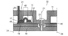
図7A、図7Bは、樹脂構造体11を用いたモジュール26の高強度化メカニズムを説明する断面図である。図7A、図7Bにおいて、半田27(半田27は鉛フリー半田を含む。なお導電性接着剤等でも半田の代用となるだけの機能があれば、これも半田の一種とする)にて、プリント基板24に形成したスルーホール等と、接続配線20とを接続する。   7A and 7B are cross-sectional views illustrating a mechanism for increasing the strength of the module 26 using the resin structure 11. 7A and 7B, printing is performed with solder 27 (solder 27 includes lead-free solder. If a conductive adhesive or the like has a function that can substitute for solder, this is also a type of solder). A through hole or the like formed in the substrate 24 is connected to the connection wiring 20.

なお、プリント基板24は多層プリント基板24としても良く、また配線孔13はスルーホールまたはスルーホールメッキも含むとしてもよい。なお図7A,図7Bにおいて、プリント基板24の表層や内層に形成した銅箔パターンやスルーホール等は図示していない。   The printed circuit board 24 may be a multilayer printed circuit board 24, and the wiring hole 13 may include through holes or through hole plating. 7A and 7B, a copper foil pattern, a through hole, and the like formed on the surface layer and the inner layer of the printed board 24 are not shown.

なお、プリント基板24の配線孔13と、ここに挿入した接続配線20との半田27による接続の場合、余分な半田27が下部に垂れたり、流れたりする場合がある。こうした場合、後述する図27Bのように、プリント基板24と、樹脂構造体11との間に隙間を形成することで、半田27の流れを制御し、目視検査できる。   In addition, when the wiring hole 13 of the printed circuit board 24 and the connection wiring 20 inserted here are connected by the solder 27, the extra solder 27 may hang down or flow downward. In such a case, the flow of the solder 27 can be controlled and visually inspected by forming a gap between the printed board 24 and the resin structure 11 as shown in FIG. 27B described later.

以上のように、接続配線20及び樹脂構造体11の一部以上は、放熱基板16の一部以上に形成しており、接続配線20は、伝熱層18から略垂直に折り曲げている放熱基板16とすることで、放熱基板16とプリント基板24との接続信頼性や固定強度を高める。なお略垂直とした場合は、90度±10度以下が望ましい。90度±10度より大きくなった場合、樹脂構造体11に設けた取付孔12へ接続配線20を挿入しにくくなる場合がある。   As described above, a part or more of the connection wiring 20 and the resin structure 11 are formed on a part or more of the heat dissipation board 16, and the connection wiring 20 is bent substantially vertically from the heat transfer layer 18. The connection reliability and the fixing strength between the heat dissipation board 16 and the printed circuit board 24 are increased by setting it to 16. In the case of being substantially vertical, 90 degrees ± 10 degrees or less is desirable. When it becomes larger than 90 ° ± 10 °, it may be difficult to insert the connection wiring 20 into the mounting hole 12 provided in the resin structure 11.

図7Aは、ネジ22によって、プリント基板24ごと、樹脂構造体11を放熱基板16に固定した様子を説明する。図7Aに示すように、ネジ22等によって、プリント基板24も、金属板19や金属板19を固定する機器のシャーシ等(シャーシ等は図示していない)に直接、固定する。   FIG. 7A illustrates a state in which the resin structure 11 is fixed to the heat dissipation substrate 16 together with the printed circuit board 24 with the screws 22. As shown in FIG. 7A, the printed circuit board 24 is also directly fixed to the chassis of the device to which the metal plate 19 and the metal plate 19 are fixed (the chassis and the like are not shown) by screws 22 and the like.

図7Bは、プリント基板24を、樹脂構造体11から離した場合について説明する断面図である。図7Bでは、樹脂構造体11で部分的に強化した放熱基板16の、接続配線20を用いて、プリント基板24を固定する。こうすることで、プリント基板24側に引張り力が発生しても、ネジ22等による押付け力が、樹脂構造体11を放熱基板16側に押付けることで、この引張り力を打ち消す。   FIG. 7B is a cross-sectional view illustrating a case where the printed board 24 is separated from the resin structure 11. In FIG. 7B, the printed circuit board 24 is fixed using the connection wiring 20 of the heat dissipation board 16 partially reinforced with the resin structure 11. Thus, even if a tensile force is generated on the printed circuit board 24 side, the pressing force by the screw 22 or the like cancels the tensile force by pressing the resin structure 11 on the heat radiating substrate 16 side.

なお、パワー半導体等の熱は、リードフレーム17を介して広がり、熱伝導性に優れた伝熱層18を介して放熱用の金属板19に広がる。その結果、パワー半導体等の発生した熱は、プリント基板24に伝わりにくいため、プリント基板24に実装した一般電子部品25等への熱的影響を抑える。   The heat of the power semiconductor or the like spreads through the lead frame 17 and spreads to the heat radiating metal plate 19 through the heat transfer layer 18 having excellent thermal conductivity. As a result, the heat generated by the power semiconductor or the like is difficult to be transmitted to the printed circuit board 24, so that the thermal influence on the general electronic component 25 mounted on the printed circuit board 24 is suppressed.

なお、樹脂構造体11を用いて、接続配線20を高精度に位置決めでき、複数の接続配線20のプリント基板24への接続性を高める。   In addition, the connection wiring 20 can be positioned with high accuracy using the resin structure 11, and the connectivity of the plurality of connection wirings 20 to the printed circuit board 24 is improved.

なおネジ22の取付け位置等は、モジュール26の大きさや形状に応じて最適な位置とすればよい。またネジ22の取り付け位置や樹脂構造体11の形状を、使用する各種部品に応じて最適値に設計することで、強度や耐振動性を高める。   The mounting position of the screw 22 may be an optimal position according to the size and shape of the module 26. In addition, the strength and vibration resistance are improved by designing the attachment position of the screw 22 and the shape of the resin structure 11 to optimum values according to the various components used.

また樹脂構造体11の固定方法は、ネジ22に限定するものではなく、樹脂構造体11の一部等に形成した構造体(例えば、爪構造やひっかけ構造、楔構造等)としてもよい。   The fixing method of the resin structure 11 is not limited to the screw 22 and may be a structure formed on a part of the resin structure 11 (for example, a claw structure, a hook structure, a wedge structure, or the like).

なお、樹脂構造体11の中央部等に開口部14を形成することで、放熱基板16に実装したパワー半導体等を目視検査することができるが、必ずしも樹脂構造体11に開口部14を形成する必要はない。   In addition, although the power semiconductor etc. which were mounted in the thermal radiation board | substrate 16 can be visually inspected by forming the opening part 14 in the center part etc. of the resin structure 11, the opening part 14 is not necessarily formed in the resin structure 11. FIG. There is no need.

また、樹脂構造体11を用いることで更に樹脂構造体11をネジ22等で固定することで、放熱基板16あるいは放熱構造体基板10全体を、構造的に一種の枠(ラーメン)構造とすることになり、その高強度化(耐振動性の向上も含む)が可能となる。また樹脂構造体11は、容易に取替え可能なため、リペーアーやメンテナンス、交換等が容易になるため、実用性を高めることができる。   Further, by using the resin structure 11 and further fixing the resin structure 11 with screws 22 or the like, the heat dissipation substrate 16 or the entire heat dissipation structure substrate 10 is structurally a kind of frame (ramen) structure. Thus, it is possible to increase the strength (including improving vibration resistance). Further, since the resin structure 11 can be easily replaced, repayment, maintenance, replacement, and the like are facilitated, so that practicality can be improved.

(実施の形態5)
次に実施の形態5として、図1等で説明した樹脂構造体11を用いて、トランスやチョーク、コネクタ等の大型部品あるいは異形部品等の電子部品(以下、異形電子部品と称す)を固定する様子について、図面を参照しながら説明する。
(Embodiment 5)
Next, as a fifth embodiment, using the resin structure 11 described with reference to FIG. 1 or the like, large parts such as transformers, chokes, and connectors, or electronic parts such as irregular parts (hereinafter referred to as irregular electronic parts) are fixed. The state will be described with reference to the drawings.

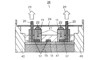
図8A、図8Bは、異形電子部品29を、保持部である固定部材30を用いて固定する様子を斜視図である。   8A and 8B are perspective views showing a state in which the odd-shaped electronic component 29 is fixed using a fixing member 30 that is a holding portion.

図8Aは、樹脂構造体11の一面以上に異形電子部品29を、固定部材30を用いて固定する様子を示す斜視図である。図8Aにおける点線28は、異形電子部品29が装着される部分例えば、樹脂構造体11の裏面、あるいは樹脂構造体11の放熱基板16側を示す。保持部である固定部材30は、金具(例えば、バネや止め具)やネジ22等であってもよいが、接着剤等を含んでも、あるいは接着剤(両面テープ等も含む)等と併用し、これを固定部材30としてもよい。また、樹脂構造体11の表面に、異形電子部品29を装着あるいは固定しやすいような凹凸等を設けることは有用である。   FIG. 8A is a perspective view illustrating a state in which the odd-shaped electronic component 29 is fixed to one or more surfaces of the resin structure 11 using the fixing member 30. A dotted line 28 in FIG. 8A indicates a portion where the odd-shaped electronic component 29 is mounted, for example, the back surface of the resin structure 11 or the heat dissipation substrate 16 side of the resin structure 11. The fixing member 30 as the holding portion may be a metal fitting (for example, a spring or a stopper), a screw 22 or the like, but may include an adhesive or the like, or may be used in combination with an adhesive (including a double-sided tape or the like). This may be the fixing member 30. In addition, it is useful to provide unevenness or the like on the surface of the resin structure 11 so that the odd-shaped electronic component 29 can be easily mounted or fixed.

ここで異形電子部品29とは、例えば、トランスやチョークコイル等のコイル部品やコネクタ、あるいは電気二重層キャパシタやリチウムイオン電池等の蓄電機器、あるいは形状が大型、あるいは異形、あるいは重量の大きな電子部品の総称とする。なお、チップ部品等のプリント基板24に表面実装可能な電子部品は、一般電子部品25とする。なおパワー半導体等は、一般電子部品25としても、異形電子部品29としてもよい。これは樹脂構造体11によって、その取付け強度や耐振性を高めることで、異形電子部品29とすることができる。なお異形電子部品29と一般電子部品25とは、取付強度の要求度や、放熱の要求度等で、判断してもよい。   Here, the odd-shaped electronic component 29 is, for example, a coil component or connector such as a transformer or choke coil, or a power storage device such as an electric double layer capacitor or a lithium ion battery, or an electronic component having a large shape, irregular shape, or heavy weight. It is a general term. An electronic component such as a chip component that can be surface-mounted on the printed circuit board 24 is a general electronic component 25. The power semiconductor or the like may be the general electronic component 25 or the odd-shaped electronic component 29. By using the resin structure 11 to increase its mounting strength and vibration resistance, the odd-shaped electronic component 29 can be obtained. Note that the odd-shaped electronic component 29 and the general electronic component 25 may be determined based on a required degree of mounting strength, a required degree of heat dissipation, or the like.

なお異形電子部品29は、5g以上、望ましくは10g以上等の重量を有するものとしてもよい。これは5g未満の部品例えば一般電子部品25等は、取り付けが容易であり、また振動等で剥れたり外れたりしにくいである。一方、5g以上、特に10g以上、更には20g以上の異形電子部品29は、取り付けが難しく、重量が大きい分だけ、振動等の影響を受けて剥がれたり外れたりしやすい。そのためこのような異形電子部品29は、その固定や実装に樹脂構造体11を利用することが望ましい。   The odd-shaped electronic component 29 may have a weight of 5 g or more, preferably 10 g or more. This is because a component of less than 5 g, for example, the general electronic component 25 or the like is easy to attach and is difficult to peel off or come off due to vibration or the like. On the other hand, the odd-shaped electronic component 29 having a weight of 5 g or more, particularly 10 g or more, and even 20 g or more is difficult to be attached and is easily peeled off or removed due to the influence of vibration or the like due to its large weight. Therefore, it is desirable to use the resin structure 11 for fixing and mounting the odd-shaped electronic component 29.

図8Bは、異形電子部品29の一部に、樹脂構造体11にネジ止めするための取付け孔12を設けた様子を示す斜視図である。図8Bのように、異形電子部品29側に、樹脂構造体11に取り付けるための構造(例えば、取付け孔12等)を設けることは有用である。また樹脂構造体11と、異形電子部品29とを、一体化したものとしてもよい。後述する図11で説明するように、例えば異形電子部品29例えば、コアや巻き線等からなるコイル部品を、樹脂で射出成型あるいはインサート成型することで、異形電子部品29を樹脂構造体11の一部に一体化成型してもよい。   FIG. 8B is a perspective view showing a state in which a mounting hole 12 for screwing the resin structure 11 is provided in a part of the odd-shaped electronic component 29. As shown in FIG. 8B, it is useful to provide a structure for attaching to the resin structure 11 (for example, the attachment hole 12) on the odd-shaped electronic component 29 side. The resin structure 11 and the odd-shaped electronic component 29 may be integrated. As will be described later with reference to FIG. 11, for example, the odd-shaped electronic component 29, for example, a coil component made of a core, a winding wire, or the like is injection-molded or insert-molded with resin, so that the odd-shaped electronic component 29 is one of the resin structures 11. You may integrally mold to a part.

図8Aにおいて、樹脂構造体11の外周部等には、樹脂構造体11を放熱基板16に固定し、放熱構造体基板10とするための取付け孔12や、放熱基板16のリードフレーム17の一部である接続配線20を保護するための配線孔13を形成している。   In FIG. 8A, the resin structure 11 is fixed to the heat dissipation board 16 on the outer periphery of the resin structure 11, and the mounting holes 12 for forming the heat dissipation structure board 10 and one of the lead frames 17 of the heat dissipation board 16. A wiring hole 13 is formed to protect the connection wiring 20 as a part.

図9は、放熱基板16と樹脂構造体11との間に、異形電子部品29を内蔵した様子を説明する斜視図である。図9において、異形電子部品29や保持部である固定部材30は、共に点線28で記載しているが、これは樹脂構造体11の裏面側(放熱基板16側)に固定していることを示すためである。裏面側に固定することで、異形電子部品29を樹脂構造体11と、放熱基板16との間にコンパクトに収納できる。また異形電子部品29と、リードフレーム17との電気的接続を容易にする。   FIG. 9 is a perspective view illustrating a state in which the odd-shaped electronic component 29 is built in between the heat dissipation board 16 and the resin structure 11. In FIG. 9, the odd-shaped electronic component 29 and the fixing member 30 that is a holding part are both indicated by a dotted line 28, but this indicates that this is fixed to the back surface side (heat radiation board 16 side) of the resin structure 11. It is for showing. By fixing to the back surface side, the odd-shaped electronic component 29 can be stored compactly between the resin structure 11 and the heat dissipation board 16. Further, the electrical connection between the odd-shaped electronic component 29 and the lead frame 17 is facilitated.

なお、異形電子部品29の樹脂構造体11への固定は、樹脂構造体11自体の形状を工夫してもよいし、保持部である固定部材30等を用いてもよい。   For fixing the odd-shaped electronic component 29 to the resin structure 11, the shape of the resin structure 11 itself may be devised, or a fixing member 30 that is a holding portion may be used.

図9において、接続配線20は、伝熱層18から略垂直に折り曲げ、樹脂構造体11から突き出しているが、伝熱層18の側面側へそのまま(折り曲げることなく)突き出したものでもよい。   In FIG. 9, the connection wiring 20 is bent substantially perpendicularly from the heat transfer layer 18 and protrudes from the resin structure 11, but may be protruded as it is (without being bent) to the side surface side of the heat transfer layer 18.

図9における矢印21は、放熱基板16の上に、異形電子部品29の一部以上を固定した樹脂構造体11が、ネジ22によって固定する様子を示す。   An arrow 21 in FIG. 9 indicates that the resin structure 11 in which a part or more of the odd-shaped electronic component 29 is fixed on the heat dissipation substrate 16 is fixed by the screw 22.

また、このネジ22によって固定した樹脂構造体11の一部は、リードフレーム17や、接続配線20の一部(あるいは略垂直に折り曲げた接続配線20の根元や根元付近)に密着し、これらを固定、補強する。   Further, a part of the resin structure 11 fixed by the screw 22 is in close contact with the lead frame 17 and a part of the connection wiring 20 (or the base of the connection wiring 20 bent substantially vertically or near the base). Fix and reinforce.

こうして、金属板19と、この上に形成したシート状の伝熱層18と、この伝熱層18に固定したリードフレーム17と、このリードフレーム17の一部を伝熱層18から突き出してなる接続配線20と、この接続配線20の異形電子部品29以上を固定する樹脂構造体11と、異形電子部品29と、から構成され、異形電子部品29の一部以上は、樹脂構造体11を用いて固定し、接続配線20の根元部の一部以上は、樹脂構造体11によって伝熱層18に押付けられているモジュール26とする。   Thus, the metal plate 19, the sheet-like heat transfer layer 18 formed thereon, the lead frame 17 fixed to the heat transfer layer 18, and a part of the lead frame 17 protrude from the heat transfer layer 18. The connection wiring 20, the resin structure 11 that fixes the odd-shaped electronic component 29 or more of the connection wiring 20, and the odd-shaped electronic component 29 are configured, and a part or more of the odd-shaped electronic component 29 uses the resin structure 11. At least a part of the base portion of the connection wiring 20 is a module 26 pressed against the heat transfer layer 18 by the resin structure 11.

接続配線20の根元部とは、接続配線20の中央部から下の部分と、略垂直に折った折り目、及び折り目から10mmまでのリードフレーム17部分である。特にこの部分を、樹脂構造体11によって補強することで、放熱基板16や放熱構造体基板10の高強度化を実現する。   The root part of the connection wiring 20 is a part below the center part of the connection wiring 20, a fold line that is bent substantially vertically, and a lead frame 17 part that extends from the fold line to 10 mm. In particular, this portion is reinforced by the resin structure 11, thereby realizing high strength of the heat dissipation substrate 16 and the heat dissipation structure substrate 10.

なお接続配線20の上半分(根元部でない部分であり、接続配線20の中央部から上の部分)を、尖らせることで、樹脂構造体11等への挿入性を高めることが望ましい。   In addition, it is desirable to enhance the insertability into the resin structure 11 or the like by sharpening the upper half of the connection wiring 20 (a portion that is not a root portion and a portion above the central portion of the connection wiring 20).

なお、異形電子部品29の端子(図示していない)の一つ以上は、リードフレーム17に電気的に接続させることで、異形電子部品29への大電流の供給や、異形電子部品29の効率的な放熱にも対応できる。これは、異形電子部品29の外部接続用(あるは実装用)の端子の一つ以上を、リードフレーム17に電気的に接続している接続部を設けることで、この接続部を介して電流供給や放熱が可能となるためである。   Note that one or more terminals (not shown) of the odd-shaped electronic component 29 are electrically connected to the lead frame 17 to supply a large current to the odd-shaped electronic component 29 and to improve the efficiency of the odd-shaped electronic component 29. It can cope with general heat dissipation. This is because by providing a connection portion that electrically connects one or more terminals for external connection (or mounting) of the odd-shaped electronic component 29 to the lead frame 17, the current flows through this connection portion. This is because supply and heat dissipation are possible.

さらに、実装が難しい異形電子部品29(コイン型や円柱状、長方形等の異形部品は、基板への固定が難しい)等を、接続配線20で固定することで、車載用に要求される振動試験例えば、XYZ方向に5G〜10Gの振動を加えるような振動試験にも対応できる。   Furthermore, the vibration test required for in-vehicle use is achieved by fixing the deformed electronic component 29 (coin-shaped, cylindrical, rectangular or other deformed component that is difficult to fix to the substrate) with the connection wiring 20. For example, it can cope with a vibration test in which 5G to 10G vibration is applied in the XYZ directions.

以上のように、異形電子部品29の少なくとも一部以上は、樹脂構造体11に保持され、樹脂構造体11は金属板19もしくは伝熱層18のどちらか一方以上、もしくは金属板19を固定する機器のシャーシの、いずれか一つ以上に固定される構造部を有している放熱構造体基板10とすることで、異形電子部品29の固定強度を高める。   As described above, at least a part of the odd-shaped electronic component 29 is held by the resin structure 11, and the resin structure 11 fixes one or more of the metal plate 19 and the heat transfer layer 18 or the metal plate 19. Fixing strength of the odd-shaped electronic component 29 is increased by using the heat dissipation structure substrate 10 having a structure part fixed to any one or more of the chassis of the device.

なお、異形電子部品29の少なくとも一部以上(一部以上は全部も含む)を、樹脂構造体10の一部で保持することは有用である。さらに異形電子部品29の一部以上を、樹脂構造体11のみならず接続配線20に保持させることで、異形電子部品29の固定強度を高めることができる。なお接続配線20に、金属板19もしくは伝熱層18のどちらか一方以上、もしくは金属板19を固定する機器のシャーシの、に固定される構造部を設ける。こうすることで、異形電子部品29を、接続配線20を介して、間接的に金属板19もしくは伝熱層18のどちらか一方以上、更には金属板19を固定する機器のシャーシ(シャーシは筐体等も含む)に高強度に固定できる。   Note that it is useful to hold at least a part of the odd-shaped electronic component 29 (a part or a part of the electronic component 29 is partly included) with a part of the resin structure 10. Further, by holding a part or more of the odd-shaped electronic component 29 not only in the resin structure 11 but also in the connection wiring 20, the fixing strength of the odd-shaped electronic component 29 can be increased. The connection wiring 20 is provided with a structure portion that is fixed to at least one of the metal plate 19 and the heat transfer layer 18, or the chassis of a device that fixes the metal plate 19. By doing so, the odd-shaped electronic component 29 is indirectly connected to one or more of the metal plate 19 and the heat transfer layer 18 via the connection wiring 20, and further, the chassis of the device that fixes the metal plate 19 (the chassis is a housing). (Including body etc.) can be fixed with high strength.

図10A、図10Bは、樹脂構造体11に、異形電子部品29を固定する様子を説明する断面図である。   10A and 10B are cross-sectional views illustrating a state in which the odd-shaped electronic component 29 is fixed to the resin structure 11.

図10Aにおいて、異形電子部品29には、ネジ止め用の取付け孔12を形成している。また樹脂構造体11側にも、異形電子部品29を挿入するための開口部14や、異形電子部品29をネジ止めするための取付け孔12を形成している。   10A, the odd-shaped electronic component 29 has a mounting hole 12 for screwing. An opening 14 for inserting the odd-shaped electronic component 29 and an attachment hole 12 for screwing the odd-shaped electronic component 29 are also formed on the resin structure 11 side.

図10Bは、異形電子部品29をネジ22aで固定した樹脂構造体11を、ネジ22bによって放熱基板16(図示していない)や機器のシャーシ等に固定する様子を示す断面図である。図10Bにおいて、異形電子部品29の側面等には取り付け用の孔12を設けている。そしてこの孔12に、ネジ22等を矢印21に示すように挿入し、樹脂構造体11に固定する。このように樹脂構造体11の一部に、異形電子部品29の取付部等を設けることは有用である。   FIG. 10B is a cross-sectional view showing a state in which the resin structure 11 in which the odd-shaped electronic component 29 is fixed with the screw 22a is fixed to the heat dissipation board 16 (not shown), the chassis of the device, or the like with the screw 22b. In FIG. 10B, mounting holes 12 are provided on the side surface and the like of the odd-shaped electronic component 29. Then, a screw 22 or the like is inserted into the hole 12 as indicated by an arrow 21 and fixed to the resin structure 11. Thus, it is useful to provide a mounting portion for the odd-shaped electronic component 29 in a part of the resin structure 11.

図11は、異形電子部品29を、樹脂構造体11の一部として、樹脂構造体11に一体化した場合について説明する斜視図である。図11において、異形電子部品29は、樹脂構造体11にインサート成型されている。異形電子部品29の外部接続用の端子の一つ以上を、樹脂構造体11より突出することにより、接続配線20と接続可能になる。こうした異形電子部品29として、DC−DCコンバータ等に使われるコアや巻き線からなるチョークコイル等を使うことができる。   FIG. 11 is a perspective view illustrating a case where the odd-shaped electronic component 29 is integrated with the resin structure 11 as a part of the resin structure 11. In FIG. 11, the odd-shaped electronic component 29 is insert-molded in the resin structure 11. By protruding one or more terminals for external connection of the odd-shaped electronic component 29 from the resin structure 11, the connection wiring 20 can be connected. As the odd-shaped electronic component 29, a choke coil made of a core or windings used in a DC-DC converter or the like can be used.

なお、異形電子部品29は、樹脂構造体11にインサート成型、あるいはアウトサート成型、あるいは一体化されたものとすることで、異形電子部品29と樹脂構造体11との接合強度を高め、更には実装コストも低減できる。   The odd-shaped electronic component 29 is insert-molded, outsert-molded, or integrated with the resin structure 11 to enhance the bonding strength between the deformed electronic component 29 and the resin structure 11, and Mounting costs can also be reduced.

図12A、図12Bは、共に樹脂構造体11を用いて、異形電子部品29の一部以上を固定する様子を説明する斜視図である。図12A、図12Bにおいて、端子31は異形電子部品29の外部接続部に相当する。   12A and 12B are perspective views for explaining a state in which a part or more of the odd-shaped electronic component 29 is fixed using the resin structure 11. 12A and 12B, the terminal 31 corresponds to an external connection portion of the odd-shaped electronic component 29.

図12A、図12Bに示すように、樹脂構造体11に、異形電子部品29の端子31を取り出すための配線孔13を形成しておくことで、異形電子部品29の端子31をリードフレーム17側のみならず、樹脂構造体11の放熱基板16でない側にも取り出すことができる。こうして異形電子部品29の配線や設計の自由度を高めることができる。   As shown in FIGS. 12A and 12B, by forming the wiring hole 13 for taking out the terminal 31 of the odd-shaped electronic component 29 in the resin structure 11, the terminal 31 of the odd-shaped electronic component 29 is connected to the lead frame 17 side. In addition, the resin structure 11 can be taken out to the side other than the heat dissipation substrate 16. In this way, the degree of freedom in wiring and design of the odd-shaped electronic component 29 can be increased.

図12Aは、樹脂構造体11の裏面側(放熱基板16側)に、異形電子部品29を固定する様子を示す。図12Aの点線28は、異形電子部品29の固定部を示す。樹脂構造体11の成形性の良さを利用して、この固定部に異形電子部品29の固定用に窪みや枠、取付け用、固定用の孔等を事前に形成できる。そして固定部材30を併用することで、異形電子部品29の固定を強固にすることができる。   FIG. 12A shows a state where the odd-shaped electronic component 29 is fixed to the back surface side (the heat dissipation substrate 16 side) of the resin structure 11. A dotted line 28 in FIG. 12A indicates a fixing portion of the odd-shaped electronic component 29. By utilizing the good moldability of the resin structure 11, a recess, a frame, a mounting hole, a fixing hole, and the like can be formed in advance in the fixing portion for fixing the odd-shaped electronic component 29. And by using the fixing member 30 together, the fixing of the odd-shaped electronic component 29 can be strengthened.

なお、異形電子部品29は、予め樹脂構造体11の内部に、あるいは樹脂構造体11の一部としてインサート成型してもよい。こうすることで、樹脂構造体11と異形電子部品29とを一体化でき、取り付け強度を高め、実装コストも抑えられる。なお、保持部である固定部材30を絶縁材料で形成することで、リードフレーム17とのショートを防止できる。また固定部材30を金属片とし、積極的にリードフレーム17を接触させることで、異形電子部品29に発生した熱を保持部である固定部材30を介した放熱基板16側に逃がすことができる。この場合、金属片からなる固定部材30と接するリードフレーム17は浮島パターン(例えば他の配線パターンから電気的に独立した島状パターン)とすることが有用である。   The odd-shaped electronic component 29 may be insert-molded in advance in the resin structure 11 or as a part of the resin structure 11. By doing so, the resin structure 11 and the odd-shaped electronic component 29 can be integrated, the attachment strength is increased, and the mounting cost can be suppressed. In addition, the short circuit with the lead frame 17 can be prevented by forming the fixing member 30 as the holding portion with an insulating material. Further, by making the fixing member 30 a metal piece and positively bringing the lead frame 17 into contact, the heat generated in the odd-shaped electronic component 29 can be released to the heat radiating board 16 via the fixing member 30 as a holding portion. In this case, it is useful that the lead frame 17 in contact with the fixing member 30 made of a metal piece has a floating island pattern (for example, an island pattern electrically independent from other wiring patterns).

以上のように、異形電子部品29の外部接続用の接続部31の一つ以上を、接続配線20の金属板19と接していない面側に突出もしくは露出させている放熱基板16とすることで、異形電子部品29の配線や設置の自由度を高められる。なお露出とは、その一部が表面に見えればよい状態である。また必要に応じて、露出部を、図12Bの端子31のように突出させることで、他のプリント基板(図示していない)との接続に対応できる。   As described above, one or more of the connection portions 31 for external connection of the odd-shaped electronic component 29 are formed as the heat dissipation substrate 16 protruding or exposed on the side of the connection wiring 20 that is not in contact with the metal plate 19. The degree of freedom in wiring and installation of the odd-shaped electronic component 29 can be increased. Note that the exposure means a state in which a part of the exposure is visible on the surface. Further, if necessary, the exposed portion protrudes like the terminal 31 in FIG. 12B, so that it can be connected to another printed circuit board (not shown).

このように、放熱基板16と、樹脂構造体11との間に、放熱基板16もしくはプリント基板(図12では図示していないが、後述する図14では図示している)の少なくとも一方以上に電気的に接続された異形電子部品29を設けているモジュール26とすることで、トランスやチョーク等の振動の影響を受けやすい部品を内蔵することができ、モジュール26の高性能化、高強度化、高信頼性化に対応できる。   In this way, between the heat dissipation board 16 and the resin structure 11, at least one of the heat dissipation board 16 or the printed circuit board (not shown in FIG. 12, but shown in FIG. 14 described later) is electrically connected. By providing the module 26 with the irregularly connected electronic component 29 connected thereto, it is possible to incorporate components that are easily affected by vibrations such as a transformer and a choke. Can support high reliability.

次に図13A、図13Bを用いて異形電子部品29の取付け例について、チョークコイル等のコイルを例に説明する。図13A、図13Bは、それぞれコイル部品の断面図と、コイル部品をモジュール26に実装した場合の拡大断面図である。図13A、図13Bにおいて、コイル部品32は、コア部33とコイル部34等から構成されている。そしてコイル部品32は半田27を用いて、リードフレーム17に固定する。   Next, an attachment example of the odd-shaped electronic component 29 will be described with reference to FIGS. 13A and 13B, taking a coil such as a choke coil as an example. 13A and 13B are a sectional view of the coil component and an enlarged sectional view when the coil component is mounted on the module 26, respectively. 13A and 13B, the coil component 32 includes a core portion 33, a coil portion 34, and the like. The coil component 32 is fixed to the lead frame 17 using solder 27.

チョークコイル等のコイル部品32に発生した熱は、矢印21に示すように、伝熱層18やリードフレーム17を介して、放熱基板16や樹脂構造体11に放熱する。   Heat generated in the coil component 32 such as a choke coil is radiated to the heat dissipation substrate 16 and the resin structure 11 through the heat transfer layer 18 and the lead frame 17 as indicated by an arrow 21.

なお、図13A、図13Bに示すように、コア部33とコイル部34とを別構造とすることで、コイル部品32の全体質量を複数に分割でき、振動時の固有振動を抑えられ、耐震性を高められる。   As shown in FIG. 13A and FIG. 13B, by making the core part 33 and the coil part 34 separate structures, the entire mass of the coil component 32 can be divided into a plurality of parts, and the natural vibration during vibration can be suppressed. Increases sex.

なお、樹脂構造体11の固定方法は、ネジ22に限定するものではなく、樹脂構造体11の一部等に形成した構造部例えば、爪構造やひっかけ構造、楔構造等としてもよい。   The fixing method of the resin structure 11 is not limited to the screw 22 and may be a structure part formed on a part of the resin structure 11, for example, a claw structure, a hook structure, a wedge structure, or the like.

また、コイル部品32を、樹脂構造体11と放熱基板16との間に挟むことで、コイル部品32の取付強度を高められる。なおコイル部品32の放熱基板16への取付けにおいて、コイル部34とリードフレーム17との半田27による接続部には不要な力が加わらないような構造例えば、後述する図33等で説明する緩和構造部49や、樹脂構造体11と半田部分とが直接接しないような構造等とすることが望ましい。   Moreover, the attachment strength of the coil component 32 can be increased by sandwiching the coil component 32 between the resin structure 11 and the heat dissipation substrate 16. It should be noted that a structure in which unnecessary force is not applied to the connecting portion of the coil portion 34 and the lead frame 17 by the solder 27 when the coil component 32 is attached to the heat radiating board 16, for example, a relaxing structure described in FIG. It is desirable that the portion 49 or a structure in which the resin structure 11 and the solder portion do not directly contact each other.

このように、樹脂構造体11による押し付け力等が、直接、半田付け部分等に加わらないようにすることで、半田27等の信頼性を高められる。更に、モジュール26や放熱基板16に取り付ける異形電子部品29の部位毎に、最適な取付け位置や取付け強度を設計することが有用である。なお図13A,図13Bにおいて、リードフレーム17に実装したパワー半導体等の発熱部品等は図示していない。   Thus, the reliability of the solder 27 and the like can be improved by preventing the pressing force or the like by the resin structure 11 from being directly applied to the soldered portion or the like. Furthermore, it is useful to design an optimal mounting position and mounting strength for each part of the odd-shaped electronic component 29 to be mounted on the module 26 or the heat dissipation board 16. In FIGS. 13A and 13B, heat-generating components such as a power semiconductor mounted on the lead frame 17 are not shown.

(実施の形態6)
次に実施の形態6として、図6等で説明したモジュール26に、異形電子部品29を実装する場合について、図14を用いて説明する。
(Embodiment 6)
Next, as a sixth embodiment, a case where the odd-shaped electronic component 29 is mounted on the module 26 described with reference to FIG. 6 and the like will be described with reference to FIG.

図14は、異形電子部品29を有するモジュール26の構成を説明する斜視図である。   FIG. 14 is a perspective view illustrating the configuration of the module 26 having the odd-shaped electronic component 29.

図14において、樹脂構造体11の外周部やその一部には、樹脂構造体11を放熱基板16や放熱構造体基板10に固定するための取付け孔12や、放熱基板16のリードフレーム17の一部である接続配線20を保護するための配線孔13を形成する。   In FIG. 14, an attachment hole 12 for fixing the resin structure 11 to the heat dissipation substrate 16 or the heat dissipation structure substrate 10, or a lead frame 17 of the heat dissipation substrate 16 is provided on the outer peripheral portion of the resin structure 11 or a part thereof. A wiring hole 13 for protecting a part of the connection wiring 20 is formed.

なお図14において、リードフレーム17からなる配線や、その上に実装したパワー半導体等、ソルダーレジスト等は図示していない。   In FIG. 14, the wiring composed of the lead frame 17, the power semiconductor mounted thereon, the solder resist, etc. are not shown.

樹脂構造体11の所定部分に、異形電子部品29や、異形電子部品29を取り付けるための固定部材30を固定する。こうして異形電子部品29の一部以上を樹脂構造体11で保持する。なお図14において、異形電子部品29や固定部材30は、点線28で記載しているが、これは樹脂構造体11の裏面側(放熱基板16側)に固定する例を示している。異形電子部品29は樹脂構造体11の表面側(プリント基板24側)に保持しても、裏面側に保持してもよいが、裏面側に固定することで、異形電子部品29を樹脂構造体11と、放熱基板16の両方で押さえるようにして固定でき、固定強度を高めている。   An odd-shaped electronic component 29 and a fixing member 30 for attaching the odd-shaped electronic component 29 are fixed to a predetermined portion of the resin structure 11. In this way, a part or more of the odd-shaped electronic component 29 is held by the resin structure 11. In FIG. 14, the odd-shaped electronic component 29 and the fixing member 30 are indicated by a dotted line 28, but this shows an example in which the odd-shaped electronic component 29 and the fixing member 30 are fixed to the back surface side (heat dissipation board 16 side) of the resin structure 11. The odd-shaped electronic component 29 may be held on the front surface side (printed circuit board 24 side) of the resin structure 11 or may be held on the back surface side. 11 and the heat dissipation board 16 can be fixed so as to be pressed, and the fixing strength is increased.

なお、異形電子部品29の樹脂構造体11への固定は、樹脂構造体11自体の形状を工夫してもよいし、固定部材30を用いてもよい。   For fixing the odd-shaped electronic component 29 to the resin structure 11, the shape of the resin structure 11 itself may be devised, or the fixing member 30 may be used.

図14において、放熱基板16は、金属板19と、この上に形成したシート状の伝熱層18と、この伝熱層18に固定したリードフレーム17と、このリードフレーム17の一部を伝熱層18から突き出してなる接続配線20と、から構成している。   In FIG. 14, the heat dissipation substrate 16 transmits a metal plate 19, a sheet-like heat transfer layer 18 formed thereon, a lead frame 17 fixed to the heat transfer layer 18, and a part of the lead frame 17. The connecting wiring 20 protrudes from the thermal layer 18.

なお、接続配線20は、伝熱層18から略垂直に折り曲げているが、これは矢印21に示すように、樹脂構造体11に形成した配線孔13を介して突き出し、プリント基板24に接続するためである。このように、放熱基板16の必要部分において、リードフレーム17を略垂直に折り曲げ、接続配線20とすれば良く、全ての周縁部(あるいは4辺全てで)で折り曲げる必要は無い。周縁部のリードフレーム17の一部を、略垂直に折り曲げることなく、そのまま(伝熱層18と略平行なまま)放熱基板16から外部へ突き出してもよい。   The connection wiring 20 is bent substantially perpendicularly from the heat transfer layer 18, but this protrudes through the wiring hole 13 formed in the resin structure 11 and is connected to the printed circuit board 24 as indicated by an arrow 21. Because. As described above, the lead frame 17 may be bent substantially vertically at the necessary portion of the heat dissipation substrate 16 to form the connection wiring 20, and it is not necessary to bend at all peripheral edges (or all four sides). A part of the peripheral lead frame 17 may be protruded from the heat dissipation substrate 16 as it is without being bent substantially vertically (while being substantially parallel to the heat transfer layer 18).

図14において、取付け孔12に向かう矢印21は、放熱基板16の上に、異形電子部品29の一部以上を固定した樹脂構造体11が、ネジ22によって固定され、放熱構造体基板10を構成する様子を示す。   In FIG. 14, an arrow 21 directed to the mounting hole 12 indicates that the resin structure 11 in which a part or more of the odd-shaped electronic component 29 is fixed on the heat dissipation board 16 is fixed by screws 22, thereby configuring the heat dissipation structure board 10. It shows how to do.

また、このネジ22によって固定した樹脂構造体11の一部は、リードフレーム17や、接続配線20の一部,あるいは略垂直に折り曲げた接続配線20の根元や根元付近を固定し、モジュール26全体の強度を高める。   Further, a part of the resin structure 11 fixed by the screw 22 fixes the lead frame 17, a part of the connection wiring 20, or the base of the connection wiring 20 bent substantially vertically or the vicinity of the base to fix the entire module 26. Increase the strength of.

プリント基板24の表面に実装した一般電子部品25は、放熱基板16に実装したパワー半導体等(図示していない)に、接続配線20を介して最短距離(あるいは最短線路長)で接続するため、ノイズの影響を受けない。   The general electronic component 25 mounted on the surface of the printed circuit board 24 is connected to a power semiconductor or the like (not shown) mounted on the heat dissipation board 16 through the connection wiring 20 at the shortest distance (or the shortest line length). Not affected by noise.

こうして、金属板19と、この上に形成したシート状の伝熱層18と、この伝熱層18に固定したリードフレーム17と、このリードフレーム17の一部を伝熱層18から略垂直に折り曲げてなる接続配線20と、この接続配線20の一部以上を固定する樹脂構造体11と、異形電子部品29と、金属板19と略並行に固定したプリント基板24と、から構成され、異形電子部品29の一部以上は、樹脂構造体11を用いて固定し、接続配線20の一部以上はプリント基板24に接続しているモジュール26であって、異形電子部品29を設置したモジュール26を実現する。   Thus, the metal plate 19, the sheet-like heat transfer layer 18 formed thereon, the lead frame 17 fixed to the heat transfer layer 18, and a part of the lead frame 17 are substantially perpendicular to the heat transfer layer 18. The connection wiring 20 that is bent, the resin structure 11 that fixes a part or more of the connection wiring 20, the odd-shaped electronic component 29, and the printed circuit board 24 that is fixed substantially in parallel with the metal plate 19, are formed in an irregular shape. A part or more of the electronic component 29 is fixed by using the resin structure 11, and a part or more of the connection wiring 20 is a module 26 connected to the printed circuit board 24, and the module 26 in which the odd-shaped electronic component 29 is installed. Is realized.

なお,予め樹脂構造体11の異形電子部品29の取付け部分に凹部や突起を設けておくことで取付け精度を高め、作業工数も減らすことができる。例えば、樹脂構造体11に、異形電子部品29の外形に応じた窪みや突起例えば、円柱状の異形電子部品29を埋め込む、あるいは嵌め込むための半円柱状の凹部を設ける。立方体の異形電子部品29を固定するための立方体状の凹部を設ける等を設ける。この結果、固定部材30の省略も可能となる。   In addition, by providing a concave portion or a protrusion in the attachment portion of the odd-shaped electronic component 29 of the resin structure 11 in advance, the attachment accuracy can be increased and the number of work steps can be reduced. For example, the resin structure 11 is provided with a recess or protrusion corresponding to the outer shape of the odd-shaped electronic component 29, for example, a semi-cylindrical recess for embedding or fitting the cylindrical odd-shaped electronic component 29. For example, a cubic recess for fixing the cubic odd-shaped electronic component 29 is provided. As a result, the fixing member 30 can be omitted.

また、図14に示すように、異形電子部品29を取り付けた樹脂構造体11を、ネジ22を用いて放熱基板16や放熱構造体基板10に固定することができる。   As shown in FIG. 14, the resin structure 11 to which the odd-shaped electronic component 29 is attached can be fixed to the heat dissipation substrate 16 or the heat dissipation structure substrate 10 using screws 22.

図14に示すように、異形電子部品29の固定に樹脂構造体11を用いるため、複数個の異形電子部品29であっても、様々な異なる外形の異形電子部品29であっても、樹脂構造体11に固定できる。なお、樹脂構造体11の表面側(プリント基板24側)と、裏面側(放熱基板16側)の両面に固定することで、樹脂構造体11に、表面側もしくは裏面側の片方に固定するより、より多くの異形電子部品29を固定することができるようになる。   As shown in FIG. 14, since the resin structure 11 is used to fix the odd-shaped electronic component 29, the resin structure can be used for a plurality of odd-shaped electronic components 29 or various-shaped different-shaped electronic components 29. Can be fixed to the body 11. In addition, by fixing to both the front surface side (printed circuit board 24 side) and the back surface side (heat dissipation board 16 side) of the resin structure 11, it is fixed to the resin structure 11 to one of the front surface side or the back surface side. As a result, a larger number of odd-shaped electronic components 29 can be fixed.

また、図14に示すように、樹脂構造体11に形成した配線孔13は、放熱基板16の接続配線20を保護する。また樹脂構造体11の一部は、接続配線20の根元を、放熱基板16側に押付けることで、その密着強度を高めることができる。   As shown in FIG. 14, the wiring hole 13 formed in the resin structure 11 protects the connection wiring 20 of the heat dissipation board 16. Moreover, the adhesion strength of a part of the resin structure 11 can be increased by pressing the base of the connection wiring 20 against the heat dissipation substrate 16 side.

なお、樹脂構造体11への異形電子部品29の取付け方法は、保持部である固定部材30以外に、樹脂構造体11自体を加工したもの例えば取付け孔12、取付け溝、はめ込み構造等であってもよい。そして樹脂構造体11における異形電子部品29を固定する構造部とは、樹脂構造体11における異形電子部品29の一部以上が接する部分である。そしてこの異形電子部品29を固定する構造部は、異形電子部品29用の保持部である固定部材30の取付け部分(例えば図2Aの点線28部分)、更には保持部である固定部材30を固定するための構造部含む。孔や突起等を用いて固定部材30を固定した場合、こうした孔や、突起部、更にはこの近辺部分も構造部に含む。なお,これら部分は図示していない)も。これは、固定部材30の固定部分(取付け部分、更にはこの近辺部分も含む)は、異形電子部品29を固定する構造部の一部だからである。   The modified electronic component 29 is attached to the resin structure 11 by processing the resin structure 11 itself other than the fixing member 30 as a holding portion, for example, an attachment hole 12, an attachment groove, a fitting structure, or the like. Also good. And the structure part which fixes the odd-shaped electronic component 29 in the resin structure 11 is a part which a part or more of the odd-shaped electronic component 29 in the resin structure 11 touches. And the structure part which fixes this odd-shaped electronic component 29 fixes the attachment part (for example, the dotted line 28 part of FIG. 2A) of the fixing member 30 which is a holding part for the odd-shaped electronic component 29, and also the fixing member 30 which is a holding part. Including a structural part for When the fixing member 30 is fixed using holes, protrusions, or the like, such holes, protrusions, and the vicinity thereof are also included in the structure portion. (These parts are not shown). This is because the fixing portion (including the attachment portion and also the vicinity thereof) of the fixing member 30 is a part of the structure portion for fixing the odd-shaped electronic component 29.

このように樹脂構造体11側に、異形電子部品29の形状に応じた取付け構造部あるいは固定部材30等の固定構造部を形成することで、様々な異形電子部品29の形状に対応できる。なお射出成形可能な市販の熱可塑性樹脂望ましくは、エンジニアリングプラスチックや液晶ポリマー等の高強度樹脂材料を用いることで、樹脂構造体11を作成できる。   As described above, by forming the attachment structure portion or the fixing structure portion such as the fixing member 30 corresponding to the shape of the odd-shaped electronic component 29 on the resin structure 11 side, it is possible to cope with various shapes of the odd-shaped electronic component 29. Note that a commercially available thermoplastic resin that can be injection-molded can be formed by using a high-strength resin material such as engineering plastic or liquid crystal polymer.

樹脂構造体11に固定する異形電子部品29について説明する。複数個の異形電子部品29や重量の大きな異形電子部品29を固定する場合、モジュール26の中央部付近等の最適位置に、あるいはバランスの最適位置に固定する。こうして樹脂構造体11の形状(樹脂構造体11の肉厚も含む)は、搭載する異形電子部品29の大きさや形状、個数や、重さ等を考慮して設計する。   The odd-shaped electronic component 29 fixed to the resin structure 11 will be described. When a plurality of odd-shaped electronic components 29 or heavy-shaped odd-shaped electronic components 29 are fixed, they are fixed at an optimal position near the center of the module 26 or at an optimal balance position. Thus, the shape of the resin structure 11 (including the thickness of the resin structure 11) is designed in consideration of the size, shape, number, weight, and the like of the odd-shaped electronic component 29 to be mounted.

図14等で示すように、樹脂構造体11は、一つ以上の配線孔13を有しており、放熱基板16のリードフレーム17の一部からなる接続配線20が、樹脂構造体11に設けた配線孔13を介して、プリント配線場24等の外部回路に接続することで、接続配線20の高強度化が可能となる。また図12A、図12B等で説明したように、配線孔13を介して、異形電子部品29の端子31を取り出すことで、異形電子部品29のみならずその端子31の高強度化にも対応できる。   As shown in FIG. 14 and the like, the resin structure 11 has one or more wiring holes 13, and the connection wiring 20 formed of a part of the lead frame 17 of the heat dissipation board 16 is provided in the resin structure 11. By connecting to the external circuit such as the printed wiring field 24 through the wiring hole 13, the strength of the connection wiring 20 can be increased. Further, as described with reference to FIGS. 12A, 12B, etc., by taking out the terminal 31 of the odd-shaped electronic component 29 through the wiring hole 13, it is possible to cope with not only the irregular-shaped electronic component 29 but also the strength of the terminal 31. .

また、樹脂構造体11は、外部もしくは接続配線20等から加えられた外力を、金属板19もしくは伝熱層18のどちらか一方以上、もしくは金属板19を固定する機器のシャーシ44の、いずれか一つ以上に数個所で、伝える構造部を有している。このため放熱基板16あるいは放熱構造体基板10は、外力に対する耐力を高める。なお複数個所で伝える構造部としては、例えば、樹脂構造体11のネジ22による取付け孔12等を複数個所とすればよい。これは一箇所あるいは一つのネジ22だけで樹脂構造体11を固定するより、複数個所あるいは複数のネジ22で樹脂構造体11を固定する方が、高強度化できるためである。   In addition, the resin structure 11 is either an external force applied from the outside or the connection wiring 20 or the like, either the metal plate 19 or the heat transfer layer 18 or the chassis 44 of the device that fixes the metal plate 19. It has a structure that conveys it at several locations. For this reason, the heat dissipation substrate 16 or the heat dissipation structure substrate 10 enhances the resistance to external forces. In addition, what is necessary is just to let the attachment hole 12 by the screw | thread 22 of the resin structure 11, etc. be several places as a structure part transmitted in several places, for example. This is because the strength of the resin structure 11 can be increased by fixing the resin structure 11 with a plurality of places or a plurality of screws 22 rather than fixing the resin structure 11 with only one place or a single screw 22.

(実施の形態7)
実施の形態7では、放熱基板16に実装した電子部品の高強度化について、図15A、図15Bを用いて説明する。
(Embodiment 7)
In the seventh embodiment, an increase in strength of an electronic component mounted on the heat dissipation board 16 will be described with reference to FIGS. 15A and 15B.

図15A、図15Bは、共に実施の形態1等で説明した放熱基板16あるいは放熱構造体基板10の高強度化について説明する断面図である。図15A、図15Bにおいて、一般電子部品25は、異形電子部品29としてもよい。   FIGS. 15A and 15B are cross-sectional views for explaining the increase in strength of the heat dissipation substrate 16 or the heat dissipation structure substrate 10 described in the first embodiment. 15A and 15B, the general electronic component 25 may be a deformed electronic component 29.

図15Aは、伝熱層18に固定したリードフレーム17の高強度化について説明する断面図である。図15A、図15Bにおいて、放熱基板16は、金属板19の上には、シート状の伝熱層18と、この伝熱層18に固定したリードフレーム17とから構成されている。   FIG. 15A is a cross-sectional view illustrating an increase in strength of the lead frame 17 fixed to the heat transfer layer 18. In FIG. 15A and FIG. 15B, the heat radiating substrate 16 includes a sheet-like heat transfer layer 18 and a lead frame 17 fixed to the heat transfer layer 18 on a metal plate 19.

次に、図15Aに示すように、放熱基板16の上に、一般電子部品25あるいは異形電子部品29を矢印21に示すように実装する。なお実装用の半田27等は図示していない。そして、一般電子部品25の一部以上を覆うように、樹脂構造体11をセットし、最後にネジ22等で固定する。   Next, as shown in FIG. 15A, the general electronic component 25 or the odd-shaped electronic component 29 is mounted on the heat dissipation board 16 as indicated by the arrow 21. The mounting solder 27 and the like are not shown. Then, the resin structure 11 is set so as to cover a part or more of the general electronic component 25, and finally fixed with screws 22 or the like.

ここで、一般電子部品25としては、パワー半導体(パワートランジスタやパワーFET)を含む。なお、異形電子部品29,例えば、表面実装が難しいような部品、電解コンデンサや電気二重層キャパシタ、トランスやチョーク等を同様に固定してもよい。   Here, the general electronic component 25 includes a power semiconductor (power transistor or power FET). The odd-shaped electronic component 29, for example, a component that is difficult to be mounted on the surface, an electrolytic capacitor, an electric double layer capacitor, a transformer, a choke, or the like may be similarly fixed.

図15Bは、リードフレーム17等の固定後の状態を説明する断面図である。図15Bに示すように、放熱基板16や、この上に実装した一般電子部品25を、伝熱層18側に樹脂構造体11を用いて、固定することで、これら部材を更に高強度化できる。なお、図15Bにおいて、一般電子部品25と、樹脂構造体11との間には隙間を設けているが、充分な強度を有する一般電子部品25であれば、樹脂構造体11に直接、接するようにあるいは隙間を設けないようにして、直接押し付けるようにしてもよい。また、この隙間の部分に、弾性体あるいは放熱用のゴム等を挿入してもよい。なお、半田付け等の応力によって信頼性が影響を受ける部位は、避ければよい。   FIG. 15B is a cross-sectional view illustrating a state after the lead frame 17 and the like are fixed. As shown in FIG. 15B, these members can be further strengthened by fixing the heat dissipation substrate 16 and the general electronic component 25 mounted thereon using the resin structure 11 on the heat transfer layer 18 side. . In FIG. 15B, a gap is provided between the general electronic component 25 and the resin structure 11. However, if the general electronic component 25 has sufficient strength, the resin structure 11 may be in direct contact. Alternatively, it may be pressed directly without providing a gap. Further, an elastic body or heat radiation rubber or the like may be inserted into the gap. It should be noted that a portion whose reliability is affected by a stress such as soldering may be avoided.

なお、図15Bにおける矢印21は、リードフレーム17等に加わる振動や引張り力、ネジ22による樹脂構造体11への押付け力等を示している。そしてこれらの力は、図15Bに示すように、金属板19に固定した樹脂構造体11によって吸収あるいは打ち消され、緩和される。   Note that an arrow 21 in FIG. 15B indicates the vibration or tensile force applied to the lead frame 17 or the like, the pressing force against the resin structure 11 by the screw 22, and the like. These forces are absorbed or canceled by the resin structure 11 fixed to the metal plate 19 and relaxed as shown in FIG. 15B.

なお、図15Bにおいて、一般電子部品25が発熱した場合、この熱は、リードフレーム17を介して広がりあるいはヒートスプレッドし、伝熱層18を介して金属板19等へと放熱することになる。   In FIG. 15B, when the general electronic component 25 generates heat, this heat spreads or heat spreads through the lead frame 17 and is radiated to the metal plate 19 or the like through the heat transfer layer 18.

(実施の形態8)
実施の形態8では、接続配線20の一部を、樹脂構造体11を介して外部回路と接続可能な端子部39を設ける場合について説明する。
(Embodiment 8)
In the eighth embodiment, a case will be described in which a part of the connection wiring 20 is provided with a terminal portion 39 that can be connected to an external circuit through the resin structure 11.

図16は、樹脂構造体11に設けた、外部回路との接続可能な端子39について説明する斜視図である。   FIG. 16 is a perspective view illustrating a terminal 39 provided on the resin structure 11 and connectable to an external circuit.

図16は、ガイド溝35、ガイド孔36、コネクタピン37、コネクタ38、接続用端子部39を示す。なお、ガイド溝35は誘いガイド等と呼ばれる形状も含む。ガイド孔36は、貫通しないくぼみ状の凹みや貫通孔も含む。コネクタ38につながるケーブル等は図示していない。   FIG. 16 shows guide grooves 35, guide holes 36, connector pins 37, connectors 38, and connection terminal portions 39. The guide groove 35 includes a shape called an invitation guide or the like. The guide hole 36 also includes a hollow that does not penetrate or a through hole. A cable connected to the connector 38 is not shown.

このように、樹脂構造体11に、コネクタ38等の挿入等を補助するガイド溝35やガイド孔35等の構造部を設けることは有用である。   As described above, it is useful to provide the resin structure 11 with structural portions such as the guide groove 35 and the guide hole 35 that assist the insertion of the connector 38 and the like.

点線28は省略を意味し、点線28によって放熱基板16の中央部等に形成したリードフレーム17からなる配線パターンやリードフレーム17に実装した発熱部品(例えば、パワー半導体、パワーLED、高出力レーザー素子、トランスやコイル等)を省略する。   The dotted line 28 means omission, and a wiring pattern formed of the lead frame 17 formed in the central portion of the heat dissipation board 16 by the dotted line 28 and a heat generating component mounted on the lead frame 17 (for example, power semiconductor, power LED, high-power laser element) , Transformers, coils, etc.) are omitted.

図16に示す樹脂構造体11は、その中央部等にコネクタ38を挿入するための接続用端子部39があり、その中にはリードフレーム17の一部を折曲げてなる接続配線20の一部が露出している。そしてコネクタ38を矢印21に示すように、接続用端子部39に挿入することで、コネクタピン37と、接続配線20との接続性を高める。コネクタピン37はバネ付のものとすることで、コンタクト性を高められる。なお、ガイド溝35やガイド孔36は、コネクタ38の取付け性や取外し性(固定性、位置決め性、挿入性)等を高める。   The resin structure 11 shown in FIG. 16 has a connection terminal portion 39 for inserting a connector 38 at the center or the like, in which a part of the connection wiring 20 formed by bending a part of the lead frame 17 is provided. The part is exposed. Then, the connector 38 is inserted into the connection terminal portion 39 as indicated by the arrow 21, thereby enhancing the connectivity between the connector pin 37 and the connection wiring 20. The connector pin 37 is provided with a spring, so that the contact property can be improved. The guide groove 35 and the guide hole 36 enhance the attachment and detachability of the connector 38 (fixability, positioning property, insertability) and the like.

図16において、樹脂構造体11の一部は、直接、金属板19に固定している。ここで金属板19への固定は、取付け孔12を用い、ここにネジ22やピン、固定具(共に図示していない)を挿入することで行う。このように樹脂構造体11を、直接、金属板19に固定することで、リードフレーム17や接続配線20、あるいは伝熱層18の一部以上も、同時に金属板19に押し当て、機械的に固定する。   In FIG. 16, a part of the resin structure 11 is directly fixed to the metal plate 19. Here, the fixing to the metal plate 19 is performed by using the mounting hole 12 and inserting a screw 22, a pin, and a fixture (both not shown). By directly fixing the resin structure 11 to the metal plate 19 in this way, a part of the lead frame 17, the connection wiring 20, or the heat transfer layer 18 is simultaneously pressed against the metal plate 19, and mechanically. Fix it.

図16における放熱構造体基板10は、金属板19と、この金属板19の上に形成したシート状の伝熱層18と、この伝熱層18に固定したリードフレーム17と、このリードフレーム17の一部を折曲げてなる接続配線20と、この接続配線20もしくはリードフレーム17のどちらかあるいは両方の一部以上を固定する樹脂構造体11とからなる。そしてこの樹脂構造体11の一部以上を金属板19に固定すると共に、この樹脂構造体11の一部に接続配線20の一部を露出させ、接続用端子部39としている。   A heat dissipation structure substrate 10 in FIG. 16 includes a metal plate 19, a sheet-like heat transfer layer 18 formed on the metal plate 19, a lead frame 17 fixed to the heat transfer layer 18, and the lead frame 17. The connection wiring 20 is formed by bending a part of the resin structure 11 and the resin structure 11 that fixes a part or both of the connection wiring 20 and the lead frame 17 or more. A part or more of the resin structure 11 is fixed to the metal plate 19, and a part of the connection wiring 20 is exposed to a part of the resin structure 11 to form a connection terminal portion 39.

なお、図16に示すように、リードフレーム17の一部以上は、伝熱層18から引き剥がされ、接続配線20とすることで、接続配線20と金属板19との間の沿面距離(一種の絶縁距離)を設ける。なお、図16において、リードフレーム17の一部以上は、伝熱層18に埋め込んでいるが、このように埋め込むことでリードフレーム17の肉厚による凹凸発生を防止する。   As shown in FIG. 16, a part or more of the lead frame 17 is peeled off from the heat transfer layer 18 to form the connection wiring 20, so that the creepage distance between the connection wiring 20 and the metal plate 19 (a kind of Insulation distance). In FIG. 16, a part or more of the lead frame 17 is embedded in the heat transfer layer 18, but the embedding due to the thickness of the lead frame 17 is prevented by embedding in this way.

図17A、図17Bは、共に接続用端子部39との高強度化について説明する断面図である。   FIG. 17A and FIG. 17B are cross-sectional views for explaining an increase in strength with the connection terminal portion 39.

図17Aに示すようにネジ22等を用いて、樹脂構造体11の一部を直接、金属板19等に固定する。図17Aにおいて、樹脂構造体11に設けた検査用端子部39に、接続配線20の一部を露出させている。このようにすることで、コネクタ38を兼用することができ、コストダウンできる。また、この放熱基板16や放熱構造体基板10に、パワー半導体や一般電子部品25、異形電子部品29等を実装した後でも、電気的な検査を行うことができるため、信頼性を高められる。   As shown in FIG. 17A, a part of the resin structure 11 is directly fixed to the metal plate 19 or the like using screws 22 or the like. In FIG. 17A, a part of the connection wiring 20 is exposed to the inspection terminal portion 39 provided in the resin structure 11. By doing in this way, the connector 38 can be shared and cost can be reduced. Further, even after the power semiconductor, the general electronic component 25, the odd-shaped electronic component 29, etc. are mounted on the heat dissipation substrate 16 or the heat dissipation structure substrate 10, the electrical inspection can be performed, so that the reliability can be improved.

図17Bは、コネクタ38に外力(例えば円弧状の矢印21)が発生する様子を示す。コネクタ38の挿入時、あるいはコネクタ38の抜取時、更にはコネクタ38を挿入した状態で機器に組み込まれた場合も、振動等でコネクタ38に色々な外力がかかる。しかし、図17Bに示すように、ネジ22等によって、樹脂構造体11は強固に固定されているため、コネクタ38からの外力は、接続配線20やリードフレーム17に直接、伝わることが無い。その結果、コネクタ38等からの外力によって、接続配線20やリードフレーム17が剥離、脱離することがない。   FIG. 17B shows a state in which an external force (for example, an arcuate arrow 21) is generated in the connector 38. Various external forces are applied to the connector 38 due to vibration or the like when the connector 38 is inserted or removed, or when the connector 38 is inserted into the apparatus with the connector 38 inserted. However, as shown in FIG. 17B, since the resin structure 11 is firmly fixed by the screw 22 or the like, the external force from the connector 38 is not directly transmitted to the connection wiring 20 or the lead frame 17. As a result, the connection wiring 20 and the lead frame 17 are not peeled off or detached by an external force from the connector 38 or the like.

このように、樹脂構造体11によって接続用端子部39を設けた場合であっても、リードフレーム17の一部以上と伝熱層18との密着強度、もしくは伝熱層18と金属板19との密着強度、もしくは接続配線20の機械的強度等を高められ、機器の信頼性を高められる。   Thus, even when the connection terminal portion 39 is provided by the resin structure 11, the adhesion strength between a part of the lead frame 17 and the heat transfer layer 18, or the heat transfer layer 18 and the metal plate 19 It is possible to increase the adhesion strength of the wire or the mechanical strength of the connection wiring 20 and the reliability of the device.

(実施の形態9)
実施の形態9では、リードフレーム17を伝熱層18に埋め込まない場合における、リードフレーム17等の固着部の高強度化について、図18を用いて説明する。
(Embodiment 9)
In the ninth embodiment, an increase in strength of a fixing portion such as the lead frame 17 when the lead frame 17 is not embedded in the heat transfer layer 18 will be described with reference to FIG.

図18は、リードフレーム17を伝熱層18に埋め込まない場合の高強度化の一例について説明する斜視図である。   FIG. 18 is a perspective view illustrating an example of increasing the strength when the lead frame 17 is not embedded in the heat transfer layer 18.

図18に示すように、ケース40の中に、金属板19を固定する。そしてこの金属板19の上に、シート状の伝熱層18を形成し、更にリードフレーム17を固定する。シート状の伝熱層18に固定したリードフレーム17の一部を、伝熱層18から略垂直に折り曲げ、接続配線20とする。   As shown in FIG. 18, the metal plate 19 is fixed in the case 40. A sheet-like heat transfer layer 18 is formed on the metal plate 19, and the lead frame 17 is fixed. A part of the lead frame 17 fixed to the sheet-like heat transfer layer 18 is bent substantially perpendicularly from the heat transfer layer 18 to form a connection wiring 20.

樹脂構造体11には、接続配線20を貫通し保護するため配線孔13と、樹脂構造体11を金属板19やケース40に固定するための取付孔12を形成する。そして矢印21に示すように、ネジ22等を用いて樹脂構造体11を金属板19やケース40に固定する。同時に接続配線20の一部以上を、樹脂構造体11に形成した配線孔13に挿入することで、これらを保護する。なおネジ22は、ネジ22以外にボルト、ナット、ピン、金具等の固定手段で置き換えてもよい。   In the resin structure 11, a wiring hole 13 for penetrating and protecting the connection wiring 20 and an attachment hole 12 for fixing the resin structure 11 to the metal plate 19 and the case 40 are formed. Then, as shown by an arrow 21, the resin structure 11 is fixed to the metal plate 19 or the case 40 using screws 22 or the like. At the same time, a part or more of the connection wiring 20 is inserted into the wiring hole 13 formed in the resin structure 11 to protect them. The screw 22 may be replaced by a fixing means such as a bolt, a nut, a pin, and a metal fitting in addition to the screw 22.

図18に示すように、伝熱層18に固定した接続配線20の根元付近を、ネジ22等で固定した樹脂構造体11を用いて、強固に固定することで、リードフレーム17を、伝熱層18に埋め込まない場合でも、接続配線20(接続配線20の根元付近のリードフレーム17も含む)と伝熱層18との接続界面が剥離しない。   As shown in FIG. 18, the lead frame 17 is heat-transferred by firmly fixing the vicinity of the base of the connection wiring 20 fixed to the heat transfer layer 18 using the resin structure 11 fixed with screws 22 or the like. Even when not embedded in the layer 18, the connection interface between the connection wiring 20 (including the lead frame 17 near the base of the connection wiring 20) and the heat transfer layer 18 does not peel off.

なお、図18において、伝熱層18として、キャスティング法等で作成したポリイミドフィルムのような樹脂フィルムを用いることができる。こうした樹脂フィルムは硬化済みのため、この中にリードフレーム17を埋め込みことは難しいが、図18のように、樹脂フィルムの上に接着剤等を用いて、リードフレーム17を固定,あるいは必要部分に後付けした場合でも、リードフレーム17や接続配線20の高強度化が可能となる。   In FIG. 18, a resin film such as a polyimide film prepared by a casting method or the like can be used as the heat transfer layer 18. Since such a resin film has been cured, it is difficult to embed the lead frame 17 therein. However, as shown in FIG. 18, the lead frame 17 is fixed on the resin film by using an adhesive or the like on the resin film. Even when retrofitted, the strength of the lead frame 17 and the connection wiring 20 can be increased.

なお、図18において、樹脂構造体11は、金属板19に設けた取付け孔12に直接、ネジ22等で固定している。図18に示すように、ネジ22等による固定部分において、金属板19上の伝熱層18を除去しておくことで、ネジ22による締め付け力が伝熱層18に影響しない。あるいはネジ22による締め付け力で、伝熱層18にクラック等が発生を防止できる。   In FIG. 18, the resin structure 11 is directly fixed to the mounting hole 12 provided in the metal plate 19 with screws 22 or the like. As shown in FIG. 18, by removing the heat transfer layer 18 on the metal plate 19 in the fixed portion by the screw 22 or the like, the tightening force by the screw 22 does not affect the heat transfer layer 18. Alternatively, the occurrence of cracks or the like in the heat transfer layer 18 can be prevented by the tightening force of the screw 22.

次に、図19A、図19Bを用いて、ケース40を用いる効果について説明する。例えば、ケース40を、樹脂封止用の土手やダム等として用いることができる。   Next, the effect of using the case 40 will be described with reference to FIGS. 19A and 19B. For example, the case 40 can be used as a bank or a dam for resin sealing.

図19A、図19Bは、共にリードフレーム17の一部以上を、封止材で保護する様子を説明する断面図である。図19A、図19Bにおいて、封止材41は、シリコン系やエポキシ系、ポリウレタン系等の市販品を使うことができる。リードフレーム17にパワー半導体(図示していない)を実装した後、封止材41で覆うことで、更に信頼性を高めることができる。   FIGS. 19A and 19B are cross-sectional views illustrating a state in which a part or more of the lead frame 17 is protected with a sealing material. In FIG. 19A and FIG. 19B, the sealing material 41 can use a commercial item, such as a silicon type, an epoxy type, and a polyurethane type. Reliability can be further improved by mounting a power semiconductor (not shown) on the lead frame 17 and then covering with a sealing material 41.

図19Aは、リードフレーム17の一部以上を封止材41で保護した後の様子を説明する断面図である。   FIG. 19A is a cross-sectional view illustrating a state after a part or more of the lead frame 17 is protected by the sealing material 41.

図19A、図19Bは、ケース40を用いて、プリント基板24を保持する様子を説明する断面図である。図19A、図19Bにおいて、プリント基板24は、例えばガラスエポキシ樹脂等を用いた市販の多層基板である。なお、プリント基板24の表面に実装した制御用半導体やチップ部品等は図示していない。   FIG. 19A and FIG. 19B are cross-sectional views illustrating how the printed circuit board 24 is held using the case 40. 19A and 19B, the printed circuit board 24 is a commercially available multilayer board using, for example, a glass epoxy resin or the like. Note that the control semiconductor and chip components mounted on the surface of the printed circuit board 24 are not shown.

図19Aに示すように、プリント基板24に形成した配線孔13例えば、スルーホール等に、接続配線20を挿入する。その後、図19Bに示すように、半田等で固定する。   As shown in FIG. 19A, the connection wiring 20 is inserted into the wiring hole 13 formed in the printed board 24, for example, a through hole. Then, as shown in FIG. 19B, it is fixed with solder or the like.

図19Bは、プリント基板24を介して接続配線20に矢印21で示すような引っ張り力が発生した場合について説明する断面図である。接続配線20に引っ張り力が発生しても、接続配線20自体が、ネジ22等で矢印21に示すように金属板19更には金属板19を固定する機器の筐体等(図示していない)に直接固定することで、こうした引張り力を打ち消す。   FIG. 19B is a cross-sectional view illustrating a case where a tensile force as indicated by an arrow 21 is generated in the connection wiring 20 via the printed circuit board 24. Even if a tensile force is generated in the connection wiring 20, the connection wiring 20 itself is connected to the metal plate 19, as shown by an arrow 21 with a screw 22 or the like, and a casing of a device for fixing the metal plate 19 (not shown). By directly fixing to, the tensile force is counteracted.

なお、図19Bに示すように、プリント基板24と、樹脂構造体11の間に隙間を設けることが望ましい。隙間を設けることで、接続配線20部分等への半田27の付着具合,半田流れ、半田量の評価を検査することができる。   In addition, as shown in FIG. 19B, it is desirable to provide a gap between the printed circuit board 24 and the resin structure 11. By providing the gap, it is possible to inspect the adhesion state of the solder 27 to the connecting wiring 20 portion, the solder flow, and the evaluation of the solder amount.

また、図19A、図19Bにおいて、樹脂構造体11の一部が、封止材41の底面のみならず、その側面や上面等を覆うあるいは密着するようにしてもよい。こうすることで、振動等が封止材41に加えられても、これら振動を封止材41の側面や上面からも樹脂構造体11へ逃がすことができ、高強度化、高耐振動化に対応できる。   In FIG. 19A and FIG. 19B, a part of the resin structure 11 may cover or be in close contact with not only the bottom surface of the sealing material 41 but also the side surface and top surface thereof. By doing so, even if vibration or the like is applied to the sealing material 41, these vibrations can be released from the side surface or the upper surface of the sealing material 41 to the resin structure 11, so that high strength and high vibration resistance can be achieved. Yes.

(実施の形態10)
実施の形態10では、樹脂構造体11を用いて作成した、放熱基板16や放熱構造体基板10の高強度化について、図20を用いて説明する。
(Embodiment 10)
In the tenth embodiment, an increase in strength of the heat dissipation substrate 16 and the heat dissipation structure substrate 10 created using the resin structure 11 will be described with reference to FIG.

図20は、放熱基板16や放熱構造体基板10の構成を説明する斜視図である。図20において、脚42とは、樹脂構造体11の一部が、金属板19や機器のシャーシや筐体、あるいは金属板19が結合部材(シャーシや筐体、部材等は図示していない)に直接、固定するように、樹脂構造体11の一部に設けたものである。   FIG. 20 is a perspective view illustrating the configuration of the heat dissipation substrate 16 and the heat dissipation structure substrate 10. In FIG. 20, the legs 42 are a part of the resin structure 11, the metal plate 19, the chassis or casing of the device, or the metal plate 19 is a coupling member (the chassis, casing, and members are not shown). It is provided in a part of the resin structure 11 so as to be fixed directly.

図20に示す樹脂構造体11は、その中央部に開口部14があり、その中には接続配線20の一部であるリードフレーム(図示していない)に実装された一般電子部品25(なおパワー半導体等の発熱部品も含む)が見える。   The resin structure 11 shown in FIG. 20 has an opening 14 at the center thereof, in which a general electronic component 25 (not shown) mounted on a lead frame (not shown) which is a part of the connection wiring 20 (note that (Including heat-generating parts such as power semiconductors).

図20において、樹脂構造体11の周辺部等に形成した複数個の取付け孔12に、矢印21に示すように各々ネジ22等を挿入することで、樹脂構造体11を金属板19や金属板19を固定するシャーシや筐体(共に図示していない)に直接、固定する。   In FIG. 20, by inserting screws 22 or the like into a plurality of mounting holes 12 formed in the periphery of the resin structure 11 as indicated by arrows 21, the resin structure 11 is attached to the metal plate 19 or the metal plate. 19 is fixed directly to a chassis or a housing (both not shown).

図20において、金属板19の上には、シート状の伝熱層18を介して、リードフレーム(図示していない)を固定しており、リードフレーム(図示していない)の一部は、伝熱層18から外に突き出し、接続配線20を構成する。このように伝熱層18を避けるように,あるいは伝熱層18を除く部分で、樹脂構造体11を直接、金属板19や金属板19を固定するシャーシや筐体、部材等に固定する。これにより、取付け時等に伝熱層18が割れにくくなる。   In FIG. 20, a lead frame (not shown) is fixed on the metal plate 19 via a sheet-like heat transfer layer 18, and a part of the lead frame (not shown) is The connection wiring 20 is configured to protrude outward from the heat transfer layer 18. In this way, the resin structure 11 is directly fixed to the chassis, casing, member, or the like for fixing the metal plate 19 or the metal plate 19 so as to avoid the heat transfer layer 18 or in a portion excluding the heat transfer layer 18. Thereby, the heat-transfer layer 18 becomes difficult to break at the time of attachment or the like.

図20に示すように、金属板19と、この金属板19上に形成したシート状の伝熱層18と、この伝熱層18に固定したリードフレーム17と、このリードフレーム17の一部を伝熱層18から突き出してなる接続配線20と、この接続配線20の一部以上を固定する樹脂構造体11と、からなり、樹脂構造体11の一部以上は、金属板19に固定している放熱基板16,あるいは放熱構造体基板10とすることで、接続配線20の取付け強度を高める。   As shown in FIG. 20, a metal plate 19, a sheet-like heat transfer layer 18 formed on the metal plate 19, a lead frame 17 fixed to the heat transfer layer 18, and a part of the lead frame 17 are The connection wiring 20 protrudes from the heat transfer layer 18 and the resin structure 11 that fixes a part or more of the connection wiring 20. A part or more of the resin structure 11 is fixed to the metal plate 19. By using the heat dissipation substrate 16 or the heat dissipation structure substrate 10, the mounting strength of the connection wiring 20 is increased.

図21A、図21Bは、共に樹脂構造体11によって、リードフレーム17や接続配線20等の強度を高める様子を示す断面図である。図21Aに示すように、放熱基板16の上に、一部に脚42を有する樹脂構造体11をセットする。その後、ネジ22等を用いて、樹脂構造体11を、矢印21に示すように放熱基板16,望ましくは、金属板19に固定する。なお図21A、図21Bにおいて、取付け孔12等は図示していない。   FIGS. 21A and 21B are cross-sectional views showing how the strength of the lead frame 17 and the connection wiring 20 is increased by the resin structure 11. As shown in FIG. 21A, the resin structure 11 having legs 42 in part is set on the heat dissipation substrate 16. Thereafter, the resin structure 11 is fixed to the heat dissipation substrate 16, preferably the metal plate 19, as indicated by an arrow 21, using screws 22 or the like. In FIG. 21A and FIG. 21B, the attachment holes 12 and the like are not shown.

図21Bは、樹脂構造体11を放熱基板16にネジ22等を用いて固定し、放熱構造体基板10とする様子を説明する断面図である。図21Bにおいて、ネジ22は、金属板19に形成した取付け孔(図示していない)にしっかり固定している。なお金属板19に形成した取付け孔に、ネジ溝を切っておいてもよい。図21Bに示す矢印21は、接続配線20に発生する力を示す。図21Bに示すように、接続配線20に外力がかかっても、接続配線20の一部以上やリードフレーム17の一部以上を、樹脂構造体11によって、矢印21に示すように金属板19や伝熱層18にしっかり固定しているあるいはネジ22によって押し付けているため、リードフレーム17と伝熱層18との界面等が剥離することはない。   FIG. 21B is a cross-sectional view illustrating a state in which the resin structure 11 is fixed to the heat dissipation board 16 with screws 22 or the like to form the heat dissipation structure board 10. In FIG. 21B, the screw 22 is firmly fixed to an attachment hole (not shown) formed in the metal plate 19. A screw groove may be cut in the mounting hole formed in the metal plate 19. An arrow 21 illustrated in FIG. 21B indicates a force generated in the connection wiring 20. As shown in FIG. 21B, even if an external force is applied to the connection wiring 20, a part of the connection wiring 20 or a part of the lead frame 17 is removed by the resin structure 11 as shown by the arrow 21. Since the heat transfer layer 18 is firmly fixed or pressed by the screw 22, the interface between the lead frame 17 and the heat transfer layer 18 does not peel off.

なお、ネジ22を一つで使用する場合は、脚42を放熱基板16の端部に接触することにより、放熱基板16上で、樹脂構造体11の位置を規制し、樹脂構造体11を放熱基板16に安定して固定できる。これはネジ22を複数個使用することで、同じ効果を持たせることができる。   In the case where one screw 22 is used, the position of the resin structure 11 is regulated on the heat dissipation board 16 by bringing the legs 42 into contact with the end portions of the heat dissipation board 16, and the resin structure 11 is dissipated. It can be stably fixed to the substrate 16. This can have the same effect by using a plurality of screws 22.

次に図22〜図25を用いて、樹脂構造体11の形状の最適化例について説明する。樹脂構造体11は、放熱基板16の形状や用途に応じて最適化できる。   Next, an example of optimizing the shape of the resin structure 11 will be described with reference to FIGS. The resin structure 11 can be optimized according to the shape and application of the heat dissipation substrate 16.

図22は、樹脂構造体11を一つ以上とした場合について説明する斜視図である。図22の矢印21に示すように接続配線20を、樹脂構造体11bに形成した取付孔12bに挿入する。その後この樹脂構造体11bを、樹脂構造体11aに形成した取付孔12aに嵌め込む。こうすることで、接続配線20の周囲全面を樹脂構造体11bで保護することができる。なお図22に示した樹脂構造体11bにおいて、取付孔12を複数個形成しておくことで、複数本の接続配線20間の位置矯正(位置ズレ防止も含む)や曲がり防止、ショート防止が可能となる。   FIG. 22 is a perspective view illustrating a case where one or more resin structures 11 are provided. As shown by the arrow 21 in FIG. 22, the connection wiring 20 is inserted into the mounting hole 12b formed in the resin structure 11b. Thereafter, the resin structure 11b is fitted into a mounting hole 12a formed in the resin structure 11a. By doing so, the entire periphery of the connection wiring 20 can be protected by the resin structure 11b. In addition, in the resin structure 11b shown in FIG. 22, by forming a plurality of mounting holes 12, it is possible to correct the position between the plurality of connection wirings 20 (including prevention of displacement), to prevent bending, and to prevent short circuit. It becomes.

なお、図22において、樹脂構造体11aは、放熱基板(図示していない)の周辺を保護するように図示しているが、必ずしも周辺すべてを保護する必要はない。放熱基板の必要部分,あるいは必要な辺、あるいはその中央部等を選択的に保護することもできる。こうした場合樹脂構造体11aは、図20の形状(一種の額縁状)に限定することは無く、棒状(Lの字型やU字型も含む)とすればよい。また板状とすることで、放熱基板16の上に形成したリードフレーム17を全面的に覆うあるいは保護することができる。   In FIG. 22, the resin structure 11a is illustrated so as to protect the periphery of the heat dissipation substrate (not shown), but it is not always necessary to protect the entire periphery. It is also possible to selectively protect the necessary portion of the heat dissipation substrate, the necessary side, or the central portion thereof. In such a case, the resin structure 11a is not limited to the shape of FIG. 20 (a kind of frame shape), but may be a rod shape (including an L shape or a U shape). Further, by using a plate shape, the lead frame 17 formed on the heat dissipation substrate 16 can be entirely covered or protected.

なお、図22において、樹脂構造体11を複数個に分ける場合,あるいは複数個の組合せからなる樹脂構造体11とする場合、用途に応じて、その形状を最適化できる。   In FIG. 22, when the resin structure 11 is divided into a plurality of parts, or when the resin structure 11 is composed of a plurality of combinations, the shape can be optimized according to the application.

図23A、図23Bは、共に接続配線20を、樹脂構造体11に形成した配線孔13に挿入し、保護する様子を説明する斜視図である。図23Aに示すように、放熱基板16の接続配線20の近くに樹脂構造体11をセットする。その後、矢印21に示すように接続配線20を配線孔13に挿入する。樹脂構造体11の脚42を伝熱層18と金属板19の端部と接触させることにより、樹脂構造体11の一部と伝熱層18との間にリードフレーム17を位置させることができ、より強固にリードフレーム17を固定することができる。   FIG. 23A and FIG. 23B are both perspective views for explaining how the connection wiring 20 is inserted into the wiring hole 13 formed in the resin structure 11 and protected. As shown in FIG. 23A, the resin structure 11 is set near the connection wiring 20 of the heat dissipation board 16. Thereafter, the connection wiring 20 is inserted into the wiring hole 13 as indicated by an arrow 21. By bringing the legs 42 of the resin structure 11 into contact with the end portions of the heat transfer layer 18 and the metal plate 19, the lead frame 17 can be positioned between a part of the resin structure 11 and the heat transfer layer 18. The lead frame 17 can be fixed more firmly.

図23Bは、接続配線20を樹脂構造体11で保護した様子を示す斜視図である。   FIG. 23B is a perspective view showing a state where the connection wiring 20 is protected by the resin structure 11.

図24A、図24Bは、共に接続配線20を、樹脂構造体11に形成した配線孔13に挿入し、保護する様子を説明する斜視図である。図24A、図24Bにおいて、挿入部43は樹脂構造体11の脚42と勘合可能な形状とする。   FIG. 24A and FIG. 24B are both perspective views for explaining how the connection wiring 20 is inserted into the wiring hole 13 formed in the resin structure 11 and protected. 24A and 24B, the insertion portion 43 has a shape that can be fitted with the leg 42 of the resin structure 11.

図24Aに示すように、放熱基板16の接続配線20の近くに樹脂構造体11をセットする。その後、挿入部43と脚42を、一種のガイドとして、矢印21に示すように接続配線20を配線孔13に挿入する。   As shown in FIG. 24A, the resin structure 11 is set near the connection wiring 20 of the heat dissipation board 16. Thereafter, the connection wiring 20 is inserted into the wiring hole 13 as shown by the arrow 21 using the insertion portion 43 and the leg 42 as a kind of guide.

図24Bは、接続配線20を樹脂構造体11で保護した様子を示す斜視図である。図24A、図24Bに示すように、樹脂構造体11の一部に形成した脚42や、金属板19の一部等に挿入部43等を形成しておくことで、これら部材の挿入性を高める。またネジ(図示していない)を省略することができる。また図24A、図24Bにおいて、樹脂構造体11のネジ等による固定を、金属板19ではなくて金属板19を固定するシャーシや筐体(共に図示していない)に直接固定してもよい。こうすることで、作業効率を高め、固定強度を高めることができる。   FIG. 24B is a perspective view showing a state where the connection wiring 20 is protected by the resin structure 11. As shown in FIG. 24A and FIG. 24B, by inserting the insertion portion 43 or the like in the leg 42 formed in a part of the resin structure 11 or in a part of the metal plate 19 or the like, the insertability of these members can be improved. Increase. Also, a screw (not shown) can be omitted. 24A and 24B, the resin structure 11 may be fixed directly to a chassis or a housing (both not shown) for fixing the metal plate 19 instead of the metal plate 19. By doing so, the working efficiency can be increased and the fixing strength can be increased.

図25A、図25Bは、共に樹脂構造体11をネジ22によってシャーシや筐体に固定する様子を説明する斜視図である。図25A、図25Bにおいて、シャーシ44は、機器の筐体等も含む。図25Aに示すように、放熱基板16の接続配線20の近くに樹脂構造体11をセットし、矢印21に示すように接続配線20を配線孔13に挿入する。その後、図25Bに示すように、ネジ22によってシャーシ44等に直接固定する。こうすることで放熱基板16や放熱構造体基板10とシャーシ44等との固定を、同時に行うことができ、コストダウンが可能となる。   FIG. 25A and FIG. 25B are both perspective views for explaining a state in which the resin structure 11 is fixed to the chassis or the case with the screws 22. In FIG. 25A and FIG. 25B, the chassis 44 also includes a device housing and the like. As shown in FIG. 25A, the resin structure 11 is set near the connection wiring 20 of the heat dissipation board 16, and the connection wiring 20 is inserted into the wiring hole 13 as indicated by an arrow 21. Thereafter, as shown in FIG. 25B, the screws 22 are directly fixed to the chassis 44 or the like. By doing so, the heat dissipation board 16 and the heat dissipation structure board 10 can be fixed to the chassis 44 and the like at the same time, and the cost can be reduced.

図25A、図25Bにおいて、挿入部43は金属板19の一部を加工したものである。挿入部43は樹脂構造11の脚42と勘合可能な形状とする。挿入部43と脚42を、勘合することにより、樹脂構造体11と放熱基板16とシャーシ44等の固定をより強固することができる。   25A and 25B, the insertion portion 43 is obtained by processing a part of the metal plate 19. The insertion portion 43 has a shape that can be fitted with the leg 42 of the resin structure 11. By fitting the insertion portion 43 and the leg 42, the resin structure 11, the heat dissipation board 16, the chassis 44, and the like can be more firmly fixed.

なお、樹脂構造体11としては、射出成型に対応する樹脂材を用いる。こうした樹脂は成形性に富み、安価である。また必要に応じて液晶ポリマー、PPE、PEEK等の強度の高いエンジニアリング樹脂を用いてもよい。   In addition, as the resin structure 11, the resin material corresponding to injection molding is used. Such resins are rich in moldability and inexpensive. Moreover, you may use engineering resin with high intensity | strength, such as liquid crystal polymer, PPE, and PEEK, as needed.

(実施の形態11)
実施の形態11では、樹脂構造体11を用いて作成した、モジュール26等において、異形電子部品29を実装する様子について図26〜図27A、図27Bを用いて説明する。
(Embodiment 11)
In the eleventh embodiment, a state in which the odd-shaped electronic component 29 is mounted on the module 26 or the like created using the resin structure 11 will be described with reference to FIGS. 26 to 27A and 27B.

図26は、モジュール26の構成を説明する斜視図である。   FIG. 26 is a perspective view illustrating the configuration of the module 26.

図26において、樹脂構造体11の外周部等には、樹脂構造体11を放熱基板16に固定するための取付け孔12や、放熱基板16のリードフレーム17の一部である接続配線20を保護するための配線孔13を形成する。   In FIG. 26, the outer periphery of the resin structure 11 and the like protect the mounting holes 12 for fixing the resin structure 11 to the heat dissipation board 16 and the connection wiring 20 that is a part of the lead frame 17 of the heat dissipation board 16. A wiring hole 13 is formed for this purpose.

なお、図26において、リードフレーム17からなる配線や、その上に実装したパワー半導体等、ソルダーレジスト等は図示していない。   In FIG. 26, the wiring composed of the lead frame 17, the power semiconductor mounted thereon, the solder resist, etc. are not shown.

樹脂構造体11の所定部分(例えば中央部等)に形成した凹部や切り込み等に、異形電子部品29を挿入し、更に必要に応じ固定部材30を固定する。こうして異形電子部品29の一部以上を樹脂構造体11のおもて面側(プリント基板24側)に固定する。おもて面側に固定することで、異形電子部品29と放熱基板16の間に樹脂構造体11が位置し、放熱構造体11の表面に実装されている電子部品(図示されていない)や、リードフレーム17もしくは接続配線板20との絶縁性能を高めている。   The odd-shaped electronic component 29 is inserted into a concave portion or a notch formed in a predetermined portion (for example, the center portion) of the resin structure 11, and the fixing member 30 is fixed as necessary. In this way, a part or more of the odd-shaped electronic component 29 is fixed to the front surface side (printed circuit board 24 side) of the resin structure 11. By fixing to the front surface side, the resin structure 11 is positioned between the odd-shaped electronic component 29 and the heat dissipation board 16, and an electronic component (not shown) mounted on the surface of the heat dissipation structure 11 Insulation performance with the lead frame 17 or the connection wiring board 20 is enhanced.

なお、異形電子部品29の樹脂構造体11への固定は、樹脂構造体11の異形電子部品29の取付構造(あるいは嵌め込み構造)を工夫することによって、固定部材30を省略することも可能である。   For fixing the odd-shaped electronic component 29 to the resin structure 11, the fixing member 30 can be omitted by devising the mounting structure (or fitting structure) of the deformed electronic component 29 of the resin structure 11. .

図26において、放熱基板16は、金属板19と、この金属板19の上に形成したシート状の伝熱層18と、この伝熱層18に固定したリードフレーム17と、このリードフレーム17の一部を伝熱層18から突き出してなる接続配線20と、から構成している。   In FIG. 26, the heat dissipation board 16 includes a metal plate 19, a sheet-like heat transfer layer 18 formed on the metal plate 19, a lead frame 17 fixed to the heat transfer layer 18, and the lead frame 17. A part of the connection wiring 20 protrudes from the heat transfer layer 18.

なお、接続配線20は、伝熱層18から略垂直に折り曲げているが、これは矢印21に示すように、樹脂構造体11に形成した配線孔13を介して突き出し、プリント基板24に接続するためである。このように、放熱基板16の最適部分(例えば、周縁部)において、リードフレーム17を略垂直に折り曲げ、接続配線20,あるいは外部回路等への接続用の端子部等とすれば良く、全ての周縁部で折り曲げる必要はない。周縁部のリードフレーム17の一部を、略垂直に折り曲げることなく、そのまますなわち伝熱層18と略平行なまま放熱基板16から外部へ突き出してもよい。   The connection wiring 20 is bent substantially perpendicularly from the heat transfer layer 18, but this protrudes through the wiring hole 13 formed in the resin structure 11 and is connected to the printed circuit board 24 as indicated by an arrow 21. Because. As described above, the lead frame 17 may be bent substantially vertically at the optimum portion (for example, the peripheral portion) of the heat dissipation board 16 to form the connection wiring 20 or a terminal portion for connection to an external circuit or the like. There is no need to bend at the periphery. A part of the lead frame 17 at the peripheral edge may be protruded from the heat dissipation substrate 16 as it is, that is, substantially parallel to the heat transfer layer 18 without being bent substantially vertically.

図26において、取付け孔12に向かう矢印21は、放熱基板16の上に、異形電子部品29の一部以上を固定した樹脂構造体11を、ネジ22によって固定する様子を示す。   In FIG. 26, an arrow 21 toward the attachment hole 12 indicates a state in which the resin structure 11 in which a part or more of the odd-shaped electronic component 29 is fixed on the heat dissipation substrate 16 is fixed by the screw 22.

また、このネジ22によって固定した樹脂構造体11の一部は、リードフレーム17や、接続配線20の一部(あるいは略垂直に折り曲げた接続配線20の根元や根元付近)を強く押し付けるため、モジュール26全体の強度を高める。   In addition, a part of the resin structure 11 fixed by the screw 22 strongly presses the lead frame 17 and a part of the connection wiring 20 (or the base of the connection wiring 20 bent substantially vertically or the vicinity of the base). 26 increase the overall strength.

また、プリント24の表面に実装した一般電子部品25例えば、制御用半導体等は、放熱基板16に実装したパワー半導体等(図示していない)に、接続配線20を介して最短距離あるいは最短線路長で接続するため、ノイズの影響を受けない。   Further, the general electronic component 25 mounted on the surface of the print 24, for example, a control semiconductor or the like is connected to a power semiconductor or the like (not shown) mounted on the heat dissipation board 16 via the connection wiring 20 or the shortest distance or the shortest line length. Because it is connected with, it is not affected by noise.

こうして金属板19と、この金属板19上に形成したシート状の伝熱層18と、この伝熱層18に固定したリードフレーム17と、このリードフレーム17の一部を伝熱層18から略垂直に折り曲げてなる接続配線20と、この接続配線20の一部以上を固定する樹脂構造体11と、異形電子部品29と、金属板19と略並行に固定したプリント基板24と、から構成され、異形電子部品29の一部以上は、樹脂構造体11に固定し、接続配線20の一部以上はプリント基板24に接続してなるモジュール26を提供する。   Thus, the metal plate 19, the sheet-like heat transfer layer 18 formed on the metal plate 19, the lead frame 17 fixed to the heat transfer layer 18, and a part of the lead frame 17 are substantially omitted from the heat transfer layer 18. It is composed of a connection wiring 20 that is bent vertically, a resin structure 11 that fixes a part or more of the connection wiring 20, an odd-shaped electronic component 29, and a printed board 24 that is fixed substantially parallel to the metal plate 19. A module 26 is provided in which a part or more of the odd-shaped electronic component 29 is fixed to the resin structure 11 and a part or more of the connection wiring 20 is connected to the printed circuit board 24.

図27A、図27Bは、共に異形電子部品29を、放熱基板16と樹脂構造体11との間に固定した様子を説明する断面図である。   27A and 27B are cross-sectional views illustrating a state in which the odd-shaped electronic component 29 is fixed between the heat dissipation substrate 16 and the resin structure 11.

図27A、図27Bに示すように、異形電子部品29を、放熱基板16と樹脂構造体11の間に固定することで、その固定性、耐振動性等を改善する。なお異形電子部品29を樹脂構造体11側に固定するにあたり、リードフレーム17を伝熱層18側から持上げあるいは浮かせて、バネ状とすることで、耐振動性や取付け時の寸法誤差を吸収する。なおリードフレーム17を浮かせても、金属片(バスバーを兼用してもよい)からなる固定部材30を用いてもよい。そしてこの固定部材30となる金属片を、一種のバスバー(電流供給ライン、あるいはジャンパー配線)と機能させることで、リードフレーム17からなる配線の引き回しの設計の自由度を高める。また弾性構造あるいは取り付け誤差を吸収する構造とすることで、この上にセットする異形部品15の寸法バラツキを吸収する。   As shown in FIGS. 27A and 27B, fixing the odd-shaped electronic component 29 between the heat dissipation substrate 16 and the resin structure 11 improves the fixing property, vibration resistance, and the like. When fixing the odd-shaped electronic component 29 to the resin structure 11 side, the lead frame 17 is lifted or floated from the heat transfer layer 18 side to form a spring, thereby absorbing vibration resistance and dimensional errors during mounting. . Even if the lead frame 17 is floated, a fixing member 30 made of a metal piece (which may also serve as a bus bar) may be used. And the metal piece used as this fixing member 30 is made to function as a kind of bus bar (current supply line or jumper wiring), thereby increasing the degree of freedom in the design of the routing of the lead frame 17. Further, by adopting an elastic structure or a structure that absorbs attachment errors, the dimensional variation of the deformed component 15 set on the structure is absorbed.

また、図27Bに示すように、プリント基板24に設けた配線孔13を、接続配線20に挿入、半田27で固定する。こうすることで、プリント基板24側に実装した制御用の一般電子部品(図示していない)と、放熱基板16に実装したパワー半導体等(図示していない)とを、接続配線20を介して最短距離(あるいは最短線路長)で接続するため、ノイズの影響を受けない。   Further, as shown in FIG. 27B, the wiring hole 13 provided in the printed circuit board 24 is inserted into the connection wiring 20 and fixed with the solder 27. By doing so, a general electronic component for control (not shown) mounted on the printed circuit board 24 side and a power semiconductor or the like (not shown) mounted on the heat dissipation board 16 are connected via the connection wiring 20. Since it is connected with the shortest distance (or the shortest line length), it is not affected by noise.

また、図27A、図27Bに示すように、樹脂構造体11に形成した配線孔13は、放熱基板16の接続配線20を保護する。また、樹脂構造体11の一部に、凹み部15a、15bを設けることで、接続配線20の根元となるリードフレーム17を、効率的に放熱基板16側に押付けることができ、その密着強度を高める。このように凹み部15a、15bを設けることで、放熱基板16や樹脂構造体11側に反りやうねりが発生しても、確実に樹脂構造体11とリードフレーム17を接触できる。   27A and 27B, the wiring hole 13 formed in the resin structure 11 protects the connection wiring 20 of the heat dissipation board 16. Further, by providing the recesses 15a and 15b in a part of the resin structure 11, the lead frame 17 which is the base of the connection wiring 20 can be efficiently pressed against the heat dissipation substrate 16 side, and the adhesion strength thereof To increase. By providing the recesses 15a and 15b in this way, the resin structure 11 and the lead frame 17 can be reliably contacted even if warpage or undulation occurs on the heat dissipation substrate 16 or the resin structure 11 side.

また、図27Bに示すように、回路基板23と、樹脂構造体11の間に隙間を設けることで、接続配線20部分等への半田27の付着具合,半田流れ、半田量を検査できる。またこの隙間に、絶縁紙や絶縁フィルム等を挿入してもよい。こうすることで、半田付け時の半田クズ等が、樹脂構造体11の上に付着することを防止する。   Further, as shown in FIG. 27B, by providing a gap between the circuit board 23 and the resin structure 11, it is possible to inspect the adhesion state, the solder flow, and the solder amount of the solder 27 to the connection wiring 20 portion and the like. Moreover, you may insert insulating paper, an insulating film, etc. in this clearance gap. By doing so, it is possible to prevent solder scraps and the like during soldering from adhering to the resin structure 11.

(実施の形態12)
実施の形態12では、樹脂構造体11を用いて、放熱基板16の接続配線20の高強度化について、図28〜31を用いて説明する。
(Embodiment 12)
In the twelfth embodiment, an increase in strength of the connection wiring 20 of the heat dissipation board 16 using the resin structure 11 will be described with reference to FIGS.

図28は、放熱基板16の接続配線20の高強度化の一例を説明する斜視図である。図28に示すように、樹脂構造体11に形成した配線孔13に、接続配線20の一部以上を挿入することで、接続配線20を保護する。また、接続配線20同士のショートを防止し、同時に接続配線20の曲がり,歪みや傾きを矯正する。   FIG. 28 is a perspective view illustrating an example of increasing the strength of the connection wiring 20 of the heat dissipation board 16. As shown in FIG. 28, the connection wiring 20 is protected by inserting a part or more of the connection wiring 20 into the wiring hole 13 formed in the resin structure 11. Further, short-circuiting between the connection wirings 20 is prevented, and at the same time, bending, distortion and inclination of the connection wiring 20 are corrected.

図29A、図29Bは、樹脂構造体11をネジ22等の物理的手段あるいは機械的手段によって、固定する様子を説明する断面図である。このように樹脂構造体11を物理的あるいは機械的に固定する構造部,例えばネジ22等や取付け孔12等を樹脂構造体11に積極的に設けることで、樹脂構造体11を、放熱基板16等と一体化でき、その高強度化を実現する。   FIGS. 29A and 29B are cross-sectional views illustrating the manner in which the resin structure 11 is fixed by physical means such as screws 22 or mechanical means. In this way, by actively providing the resin structure 11 with a structure part for physically or mechanically fixing the resin structure 11, such as the screw 22 or the attachment hole 12, the resin structure 11 is attached to the heat dissipation substrate 16. It can be integrated with etc., and its high strength is realized.

図29A、図29Bにおける点線28は、樹脂構造体11の中央部等に形成した開口部14を示す。開口部14は、リードフレーム17を配線として、この配線上に実装した各種発熱部品,例えば、パワー半導体、パワーLED、高出力レーザー素子、トランスやコイル等(これらは図示していない)に対して、樹脂構造体11が物理的障害とならないために設けたものである。   A dotted line 28 in FIGS. 29A and 29B indicates the opening 14 formed in the central portion of the resin structure 11 or the like. The opening 14 is used for various heat generating components mounted on the wiring using the lead frame 17 as a wiring, for example, a power semiconductor, a power LED, a high-power laser element, a transformer, a coil, etc. (these are not shown). The resin structure 11 is provided so as not to be a physical obstacle.

図29Aにおいて、金属板19の上には、シート状の伝熱層18を固定しており、この伝熱層18にはリードフレームを固定している(リードフレームは図示していない)。   In FIG. 29A, a sheet-like heat transfer layer 18 is fixed on the metal plate 19, and a lead frame is fixed to the heat transfer layer 18 (the lead frame is not shown).

図29Aに示すネジ22を、矢印21に示すように樹脂構造体11に設けた取付け孔12に挿入し、樹脂構造体11を固定する。なお伝熱層18側に形成する取付け孔12の直径を、金属板19に形成する孔12より大きくすることで、金属板19の孔16にネジ山あるいはタップ溝を形成できる。図29Bは、樹脂構造体11と、リードフレーム17の一部である接続配線20とをネジ22によって、機械的に固定する様子を示す。図29Bに示すように、接続配線20を樹脂構造体11に機械的に固定することで、接続配線20に伝わった外力を、樹脂構造体11を介して金属板19等に逃がすことができる。   The screw 22 shown in FIG. 29A is inserted into the mounting hole 12 provided in the resin structure 11 as indicated by the arrow 21 to fix the resin structure 11. In addition, by making the diameter of the attachment hole 12 formed on the heat transfer layer 18 side larger than the hole 12 formed in the metal plate 19, a screw thread or a tap groove can be formed in the hole 16 of the metal plate 19. FIG. 29B shows a state in which the resin structure 11 and the connection wiring 20 that is a part of the lead frame 17 are mechanically fixed by screws 22. As shown in FIG. 29B, the external force transmitted to the connection wiring 20 can be released to the metal plate 19 or the like via the resin structure 11 by mechanically fixing the connection wiring 20 to the resin structure 11.

図30A、図30Bは、樹脂構造体11が、リードフレーム17や接続配線20、あるいは外部回路等への接続部等の一部以上を補強する構造部の一例を示す断面図である。   30A and 30B are cross-sectional views showing an example of a structure part in which the resin structure 11 reinforces a part of the lead frame 17, the connection wiring 20, or a connection part to an external circuit or the like.

図30Aは、樹脂構造体11が、リードフレーム17や、リードフレーム17の一部からなる接続配線20の根元を補強する様子を説明する断面図である。   FIG. 30A is a cross-sectional view illustrating how the resin structure 11 reinforces the lead frame 17 and the base of the connection wiring 20 formed of a part of the lead frame 17.

図30Aに示すように、樹脂構造体11を、ネジ22等で金属板19、更にはシャーシ44に固定することで、矢印21に示すような固定力が、リードフレーム17に発生する。この結果、引っ張り力(矢印21)が発生した場合でも、矢印21aに示す固定力が、この引っ張り力(矢印21)を打ち消す。   As shown in FIG. 30A, by fixing the resin structure 11 to the metal plate 19 and further to the chassis 44 with screws 22 or the like, a fixing force as shown by an arrow 21 is generated in the lead frame 17. As a result, even when a tensile force (arrow 21) is generated, the fixing force indicated by arrow 21a cancels the tensile force (arrow 21).

図30Bは、ネジ22部分での断面図である。図30Bに示すように、ネジ22と、リードフレーム17を、途中に絶縁性を有する樹脂構造体11を介して絶縁、固定することで、ネジ22によるノイズ等の影響を防止する。なお、図30Bにおける点線28は、伝熱層18の影に隠れたリードフレーム17の位置を示す。   FIG. 30B is a cross-sectional view of the screw 22 portion. As shown in FIG. 30B, the screw 22 and the lead frame 17 are insulated and fixed through the resin structure 11 having insulation properties in the middle, thereby preventing the influence of noise and the like due to the screw 22. A dotted line 28 in FIG. 30B indicates the position of the lead frame 17 hidden behind the heat transfer layer 18.

図31A、図31Bは、樹脂構造体11を、封止材41の充填に用いる様子を説明する断面図である。図31A、図31Bにおいて、ボンディングワイヤー46としては、アルミ線等を使うことができる。また、固定層47とはベアチップ45をリードフレーム17等に固定するための半田27や接着剤等からなる。   FIG. 31A and FIG. 31B are cross-sectional views illustrating how the resin structure 11 is used for filling the sealing material 41. In FIGS. 31A and 31B, an aluminum wire or the like can be used as the bonding wire 46. The fixing layer 47 is made of solder 27, an adhesive, or the like for fixing the bare chip 45 to the lead frame 17 or the like.

図31A、図31Bにおいて、放熱基板16の上には、ベアチップ45等が実装されている。またベアチップ45は、ボンディングワイヤー46等で互いに接続され、封止材41で覆われている。   31A and 31B, a bare chip 45 and the like are mounted on the heat dissipation board 16. The bare chips 45 are connected to each other by bonding wires 46 or the like and covered with a sealing material 41.

図31A、図31Bにおける矢印21は、樹脂構造体11がネジ22で金属板19等に固定されることで、接続配線20等を高強度化する様子を示す。   The arrows 21 in FIGS. 31A and 31B indicate that the strength of the connection wiring 20 and the like is increased by fixing the resin structure 11 to the metal plate 19 and the like with screws 22.

なお図31Bに示すように、ベアチップ45を実装した後、封止材41でこれらを保護することが望ましい。また封止材41の一部以上を覆うように、樹脂構造体11を形成してもよい(図示していない)。このように、樹脂構造体11が、伝熱層18に固定されたリードフレーム17や、異形電子部品29、更には後述する図32A、図32B〜図33で説明する金属箔パターン48等の部材を覆うようにすることで、これらリードフレーム17や、異形電子部品29、更には金属箔パターン48は,高強度化が可能となる。金属箔パターン48は後述する図32A、図32Bで説明する。これは樹脂構造体11をネジ22等で金属板19等に固定することによって、これら部材を覆うように設けた樹脂構造体11が、これら部材を金属板19側に押し付け、固定、保持するためである。また、このように各部材の固定強度を、樹脂構造体11で高めることで、例えば封止材41自体と下地との引き剥がし強度を実質的に高めることができ、封止材41等の材料選択の自由度を高められる。樹脂構造体11は接続配線20の根元部分を固定するだけでも、リードフレーム17にかかる力を緩和でき、リードフレーム17に実装されるベアチップ45およびボンディングワイヤー46を保護するため、封止材41自体と下地と引きはがし強度を実質的に高めることができる。   As shown in FIG. 31B, it is desirable to protect the bare chip 45 with a sealing material 41 after the bare chip 45 is mounted. Moreover, you may form the resin structure 11 so that a part or more of the sealing material 41 may be covered (not shown). Thus, the resin structure 11 is a member such as the lead frame 17 fixed to the heat transfer layer 18, the odd-shaped electronic component 29, and the metal foil pattern 48 described later with reference to FIGS. 32A and 32B to 33. By covering the lead frame 17, the lead frame 17, the odd-shaped electronic component 29, and the metal foil pattern 48 can be increased in strength. The metal foil pattern 48 will be described later with reference to FIGS. 32A and 32B. This is because the resin structure 11 provided so as to cover these members by fixing the resin structure 11 to the metal plate 19 or the like with screws 22 or the like presses these members against the metal plate 19 side, and fixes and holds them. It is. Further, by increasing the fixing strength of each member with the resin structure 11 in this way, for example, the peeling strength between the sealing material 41 itself and the base can be substantially increased, and the material such as the sealing material 41 or the like. Increase the degree of freedom of choice. The resin structure 11 can alleviate the force applied to the lead frame 17 only by fixing the base portion of the connection wiring 20, and protects the bare chip 45 and the bonding wire 46 mounted on the lead frame 17. And the substrate and the peel strength can be substantially increased.

また,図31A、図31Bに示すように、樹脂構造体11を例えば、額縁状とすることで、この樹脂構造体11で囲った部分に封止材41を注入しても、その隙間から封止材41が流れ出ることが無い。その結果、粘度の低く流動性の高い封止材41を選ぶことができ、ベアチップ45等を封止する場合にも、封止材41の中に泡例えば、空気の気泡が残りにくいため、その封止性を高める。   Further, as shown in FIGS. 31A and 31B, by forming the resin structure 11 into a frame shape, for example, even if the sealing material 41 is injected into the portion surrounded by the resin structure 11, the resin structure 11 is sealed from the gap. Stop material 41 does not flow out. As a result, the sealing material 41 having a low viscosity and high fluidity can be selected. Even when the bare chip 45 or the like is sealed, bubbles such as air bubbles hardly remain in the sealing material 41. Increase sealing performance.

なお図30A、図30Bにおいて、樹脂構造体11に形成した取付け孔12に、インサート,あるいはインサートナット、スプリュー、埋め込みナット、挿入ナット(共に図示していない)を用いてもよい。また,ネジ22の先端(ドライバやねじ回しの接しない側)を、樹脂構造体11から露出させないこと,すなわちネジ22の先端を樹脂構造体11の中に隠しておくことでネジ22と、他の配線(他の実装部品や配線も含む)との絶縁性(沿面距離も含む)を高められる。   30A and 30B, an insert, or an insert nut, a sprue, a buried nut, and an insertion nut (both not shown) may be used for the mounting hole 12 formed in the resin structure 11. Further, by not exposing the tip of the screw 22 (the side where the screwdriver or screwdriver is not in contact) from the resin structure 11, that is, by hiding the tip of the screw 22 in the resin structure 11, Insulation (including creepage distance) with the wiring (including other mounting parts and wiring) can be enhanced.

このように、樹脂構造体11をネジ22等で金属板19(更には金属板19を固定する筐体やシャーシ44。共に図示していない)に固定することで、部分的に高強度化(あるいは剥離強度を高める)できる。なお樹脂構造体11の一部は、積極的にリードフレーム17を覆い、リードフレーム17と接するようにその形状を設計することが望ましい。   In this way, the resin structure 11 is fixed to the metal plate 19 with screws 22 or the like (further, the housing or chassis 44 for fixing the metal plate 19, both not shown), so that the strength is partially increased ( Alternatively, the peel strength can be increased). It is desirable that a part of the resin structure 11 is designed so as to positively cover the lead frame 17 and be in contact with the lead frame 17.

このように、樹脂構造体11はリードフレーム17に実装されたベアチップ45を保護している、もしくはベアチップ45を封止する、封止材41の一部以上を保護もしくは覆っている放熱基板16とすることで、ベアチップ45のみならず、封止材41の高強度化が可能となる。   As described above, the resin structure 11 protects the bare chip 45 mounted on the lead frame 17, or seals the bare chip 45 and protects or covers a part or more of the sealing material 41. By doing so, not only the bare chip 45 but also the sealing material 41 can be increased in strength.

(実施の形態13)
実施の形態13では、放熱基板16に使用するリードフレーム17を、リードフレーム17と金属箔パターンとの積層体とした場合について、図32A、図32Bを用いて説明する。
(Embodiment 13)
In the thirteenth embodiment, a case where the lead frame 17 used for the heat dissipation substrate 16 is a laminate of the lead frame 17 and a metal foil pattern will be described with reference to FIGS. 32A and 32B.

図32A、図32Bは、共にアルミ基板等を利用して放熱基板16を作成する様子を説明する断面図である。   FIG. 32A and FIG. 32B are cross-sectional views for explaining how the heat dissipation substrate 16 is formed using an aluminum substrate or the like.

図32A、図32Bにおいて、金属箔パターン48を有する放熱基板16としては、例えば市販のアルミ基板例えば、ポリイミドフィルムを貼り付けたアルミ板の上に、アルミ箔や銅箔等の金属箔を用いた配線パターンを形成したものを用いることができる。こうしたアルミ基板は、金属箔をフォトエッチングによってパターニングするため、線間/線幅=50ミクロン/50ミクロンのような微細な金属箔パターン48を形成することができる。   32A and 32B, as the heat dissipation substrate 16 having the metal foil pattern 48, for example, a commercially available aluminum substrate, for example, a metal foil such as an aluminum foil or a copper foil is used on an aluminum plate to which a polyimide film is attached. What formed the wiring pattern can be used. In such an aluminum substrate, since the metal foil is patterned by photoetching, a fine metal foil pattern 48 having a line spacing / line width = 50 microns / 50 microns can be formed.

また、アルミ基板(例えば、アルミ板の上にポリイミド等の耐熱性フィルムあるいはアルミナ等のセラミック粉を熱硬化性樹脂の中に分散してなる伝熱を有する絶縁層)を介して銅箔やアルミ箔からなる端円パターンを接着したもの)が、金属基板、アルミ放熱基板、金属放熱基板等の名称で市販されており、こうしたものを用いることができる。   In addition, copper foil or aluminum via an aluminum substrate (for example, a heat-resistant film such as polyimide on an aluminum plate or an insulating layer having heat transfer formed by dispersing ceramic powder such as alumina in a thermosetting resin) A product obtained by bonding an end circle pattern made of foil) is commercially available under the names of a metal substrate, an aluminum heat dissipation substrate, a metal heat dissipation substrate, and the like, and these can be used.

なお、金属箔パターン48を構成する銅箔やアルミ箔は、厚み18ミクロン以上200ミクロン以下の電解銅やアルミ箔とする。この厚みとすることで、エッチング等を用いたことによるファインパターンの形成が容易となり、基板の小型化、高密度化に対応する。なお金属箔の厚みが18ミクロン未満の場合、熱伝導性や配線抵抗に影響を与える可能性がある。また200ミクロンを超える場合、エッチングによるファインパターン化が難しい場合がある。こうした場合、銅箔の代わりに、銅板を使うことができる。銅箔はエッチングによる加工性が優れている。銅板は金型等による加工性が優れている。   The copper foil or aluminum foil constituting the metal foil pattern 48 is an electrolytic copper or aluminum foil having a thickness of 18 microns or more and 200 microns or less. By using this thickness, it becomes easy to form a fine pattern by using etching or the like, which corresponds to a reduction in size and density of the substrate. When the thickness of the metal foil is less than 18 microns, there is a possibility of affecting the thermal conductivity and the wiring resistance. If it exceeds 200 microns, fine patterning by etching may be difficult. In such a case, a copper plate can be used instead of the copper foil. Copper foil is excellent in workability by etching. The copper plate is excellent in workability by a mold or the like.

なお、リードフレーム17をタフピッチ銅で形成することで、リードフレーム17の低コスト化や高熱伝導化が可能となる。またリードフレーム17の材料は銅に限定する必要は無く、銅合金やアルミニウム、あるいはアルミ合金等であってもよい。これは銅等が半田付け性や溶接性に優れ、アルミ等がワイヤーボンディング性等に優れているからであり、用途に応じて使い分ける。   In addition, by forming the lead frame 17 with tough pitch copper, the lead frame 17 can be reduced in cost and heat conduction. The material of the lead frame 17 need not be limited to copper, and may be copper alloy, aluminum, aluminum alloy, or the like. This is because copper and the like are excellent in solderability and weldability, and aluminum and the like are excellent in wire bonding properties and the like.

実施の形態13では、こうしたアルミ基板の所定部分に、リードフレーム17を固定し、放熱基板16とするものである。なお、アルミ基板の一部にリードフレーム17を固定することで、金属箔パターン48では対応できないような、大電流(例えば、100A)やヒートスプレッド(例えば、熱拡散性)に対応できる。   In the thirteenth embodiment, a lead frame 17 is fixed to a predetermined portion of such an aluminum substrate to form a heat dissipation substrate 16. In addition, by fixing the lead frame 17 to a part of the aluminum substrate, it is possible to cope with a large current (for example, 100 A) and heat spread (for example, thermal diffusivity) that cannot be handled by the metal foil pattern 48.

図32A、図32Bにおいて、金属板19の上には、ポリイミドフィルム等からなる伝熱層18が形成されている。また伝熱層18の表面には、銅箔やアルミニウム箔からなる金属箔パターン48が形成されている。そして金属箔パターン48の上に、必要に応じてリードフレーム17が固定されている。なお一般電子部品25(パワー半導体等も含む)は、金属箔パターン48側に実装することで、高密度実装に対応できる。またリードフレーム17側に実装することで、ヒートスプレッドや大電流に対応できる。   32A and 32B, the heat transfer layer 18 made of a polyimide film or the like is formed on the metal plate 19. A metal foil pattern 48 made of copper foil or aluminum foil is formed on the surface of the heat transfer layer 18. A lead frame 17 is fixed on the metal foil pattern 48 as necessary. The general electronic component 25 (including a power semiconductor and the like) can be mounted on the metal foil pattern 48 side to support high-density mounting. Further, mounting on the lead frame 17 side can cope with heat spread and large current.

図32Aの矢印21に示すように、樹脂構造体11を、放熱基板16に固定し、放熱構造体基板10とする。   As shown by an arrow 21 in FIG. 32A, the resin structure 11 is fixed to the heat dissipation substrate 16 to be a heat dissipation structure substrate 10.

図32Bは、樹脂構造体11で、補強された後の放熱基板16の断面図である。図32Bに示すように、リードフレーム17や金属箔パターン48の一部を、樹脂構造体11で補強することで、これら部材の高強度化,あるいは伝熱層18との接着強度を高める。またリードフレーム17の一部を、略垂直に折り曲げ、樹脂構造体11に設けた配線孔13から外部に突出させることで、この部分を外部回路等への接続用の接続配線20とすることができる。   FIG. 32B is a cross-sectional view of the heat dissipation board 16 after being reinforced with the resin structure 11. As shown in FIG. 32B, a part of the lead frame 17 and the metal foil pattern 48 is reinforced with the resin structure 11 to increase the strength of these members or increase the adhesive strength with the heat transfer layer 18. Further, a part of the lead frame 17 is bent substantially vertically and protrudes to the outside from the wiring hole 13 provided in the resin structure 11, so that this part can be used as a connection wiring 20 for connection to an external circuit or the like. it can.

図32Bにおける矢印21は、ネジ22が樹脂構造体11を介してリードフレーム17を金属板19側に押し付ける力を示す。また図32Bにおける矢印21は、接続配線20等に接続された電力ケーブル等(図示していない)からの外力を示す。図32Bに示すように、これら外力は、ネジ22等が樹脂構造体11を締め付ける力によって、打ち消される。   An arrow 21 in FIG. 32B indicates the force with which the screw 22 presses the lead frame 17 against the metal plate 19 through the resin structure 11. An arrow 21 in FIG. 32B indicates an external force from a power cable or the like (not shown) connected to the connection wiring 20 or the like. As shown in FIG. 32B, these external forces are canceled out by the force with which the screw 22 or the like tightens the resin structure 11.

このように、伝熱層18の上には、金属箔パターン48が設けられ、リードフレーム17の一部以上は、金属箔パターン48と電気的に接続された接続部を有している放熱基板16とすることで、ファインパターンの要求される部分は金属箔パターン48で、強度や大電流等が要求される部分はリードフレーム17で、と互いに回路パターンを使い分けできる。更に市販の金属箔パターン48を用いたアルミ基板の高強度化、大電流化にも対応できるため、広範囲な市場ニーズに対応できる。   As described above, the metal foil pattern 48 is provided on the heat transfer layer 18, and a part or more of the lead frame 17 has a connection part electrically connected to the metal foil pattern 48. By setting the number to 16, the circuit pattern can be used separately from the metal foil pattern 48 where the fine pattern is required, and the lead frame 17 where the strength and large current are required. Furthermore, since it can respond to the increase in strength and current of an aluminum substrate using a commercially available metal foil pattern 48, it can meet a wide range of market needs.

次に、樹脂構造体11で、リードフレーム17を固定する場合に、半田付け部分に不要な応力発生させないようにする様子について説明する。   Next, a state in which unnecessary stress is not generated in the soldered portion when the lead frame 17 is fixed with the resin structure 11 will be described.

図33は、半田付け部分に不要な応力発生をさせないようにした放熱基板16および樹脂構造体11の断面図の一例を説明する断面図である。図33において、緩和構造部49とは、例えばリードフレーム17の一部を折り曲げたものである。なお、緩和構造部49とは、例えば、樹脂構造体11と半田付け部分とが直接重ならないようにする、あるいは樹脂構造体11と半田が直接的には接しないようにする構造の部分である。   FIG. 33 is a cross-sectional view illustrating an example of a cross-sectional view of the heat dissipation board 16 and the resin structure 11 in which unnecessary stress is not generated in the soldered portion. In FIG. 33, the relaxation structure 49 is formed by bending a part of the lead frame 17, for example. The relaxation structure portion 49 is, for example, a portion of a structure that prevents the resin structure 11 and the soldered portion from directly overlapping each other or prevents the resin structure 11 and the solder from directly contacting each other. .

このように樹脂構造体11による固定力が半田付け部分に直接伝わらないようにするあるいは半田や半田付け部分に樹脂構造体11が接しない、あるいは半田や半田付け部分に樹脂構造体11の取付けに起因する応力が発生しないようにする緩和構造部49を設ける。この結果リードフレーム17に、樹脂構造体11から強い押し付け力を加えた場合でも、半田付け部分に発生する応力を小さくできる。特に、鉛フリー半田27等の応力の影響を受けやすいものに対して有用である。   Thus, the fixing force by the resin structure 11 is prevented from being directly transmitted to the soldered portion, the resin structure 11 is not in contact with the solder or the soldered portion, or the resin structure 11 is attached to the solder or the soldered portion. A relaxation structure portion 49 is provided to prevent the resulting stress from occurring. As a result, even when a strong pressing force is applied to the lead frame 17 from the resin structure 11, the stress generated in the soldered portion can be reduced. In particular, it is useful for those that are easily affected by stress such as lead-free solder 27.

図33において、金属箔パターン48の上には、リードフレーム17を半田27によって固定している。そしてリードフレーム17の半田付け部分から離れた部分を矢印21で示すように樹脂構造体11で固定することで、半田付け部分に不要な応力発生を防止する。あるいは樹脂構造体11が、直接半田付け部分を踏まない構造とできる。更にリードフレーム17の一部に緩和構造部49を設けることで、更に応力発生を防止でき、半田付け部分の信頼性を高める。   In FIG. 33, the lead frame 17 is fixed on the metal foil pattern 48 with solder 27. Then, by fixing the portion of the lead frame 17 away from the soldering portion with the resin structure 11 as indicated by an arrow 21, unnecessary stress is prevented from being generated in the soldering portion. Or the resin structure 11 can be made into the structure which does not step on a soldering part directly. Furthermore, by providing the relaxation structure portion 49 in a part of the lead frame 17, it is possible to further prevent the generation of stress and to improve the reliability of the soldered portion.

図33において半田27は、半田27(鉛フリー半田も含む)以外に、接着剤(導電性接着剤、熱伝導性絶縁性接着剤等も含む)であってもよい。例えばリードフレーム17の一部をU字型等に折り曲げてなる緩和構造部49を、樹脂構造体11を金属板19側に固定した部分と、半田27で固定した部分との間に設けることで、矢印21に示すような取付力(あるいは固定力、あるいは締め付け力)が、半田27に直接、伝わらないようにできる。このような緩和構造部49を必要に応じてリードフレーム17の一部に設けることで、応力集中等によるクラック等の発生を防止できる。   In FIG. 33, the solder 27 may be an adhesive (including a conductive adhesive, a heat conductive insulating adhesive, etc.) in addition to the solder 27 (including lead-free solder). For example, by providing a relaxation structure portion 49 formed by bending a part of the lead frame 17 into a U-shape or the like between a portion where the resin structure 11 is fixed to the metal plate 19 side and a portion where the resin structure 11 is fixed with solder 27. The mounting force (or fixing force or tightening force) as indicated by the arrow 21 can be prevented from being transmitted directly to the solder 27. By providing such a relaxation structure portion 49 in a part of the lead frame 17 as necessary, it is possible to prevent the occurrence of cracks due to stress concentration or the like.

このように、樹脂構造体11が、リードフレーム17や異形電子部品29等を固定する際、リードフレーム17や異形電子部品29等の端子31に形成された半田27へ、直接、応力が発生しない構造あるいは緩和構造部49とすること例えば、半田付け部分を避ける、樹脂構造体11が半田付け部分と接しない、あるいは応力発生を抑えることによって、半田付け部分への応力発生を防止することとができ、放熱基板16の信頼性を高められる。   As described above, when the resin structure 11 fixes the lead frame 17 or the odd-shaped electronic component 29 or the like, no stress is directly generated on the solder 27 formed on the terminal 31 of the lead frame 17 or the odd-shaped electronic component 29 or the like. For example, avoiding a soldering portion, preventing the resin structure 11 from coming into contact with the soldering portion, or suppressing the generation of stress by preventing the soldering portion from being generated. This can improve the reliability of the heat dissipation board 16.

本発明に係る放熱構造体基板は、マイルドハイブリッドカーを始めとするハイブリッドカーや電気自動車、産業用の機器に使われる放熱構造として有用である。   The heat dissipation structure substrate according to the present invention is useful as a heat dissipation structure used in hybrid cars including mild hybrid cars, electric vehicles, and industrial equipment.

10 放熱構造体基板
11 樹脂構造体
12 取付け孔
13 配線孔
14 開口部
15a,15b 凹み部
16 放熱基板
17 リードフレーム
18 伝熱層
19 金属板
20 接続配線
21 矢印
22 ネジ
23 伝熱樹脂
24 プリント基板
25 一般電子部品
26 モジュール
27 半田
28 点線
29 異形電子部品
30 固定部材
31 接続部
32 コイル部品
33 コア部
34 コイル部
35 ガイド溝
36 ガイド孔
37 コネクタピン
38 コネクタ
39 接続端子部
40 ケース
41 封止材
42 脚
43 挿入部
44 シャーシ
45 ベアチップ
46 ボンディングワイヤ―
47 固定層
48 金属箔パターン
49 緩和構造部
100 結合部
101 強化部
102 ガイド部
103 端子部
104 保持部
DESCRIPTION OF SYMBOLS 10 Heat radiation structure board 11 Resin structure 12 Mounting hole 13 Wiring hole 14 Opening part 15a, 15b Recessed part 16 Heat radiation board 17 Lead frame 18 Heat transfer layer 19 Metal plate 20 Connection wiring 21 Arrow 22 Screw 23 Heat transfer resin 24 Printed board 25 General Electronic Components 26 Module 27 Solder 28 Dotted Line 29 Variant Electronic Components 30 Fixing Member 31 Connection Portion 32 Coil Component 33 Core Portion 34 Coil Portion 35 Guide Groove 36 Guide Hole 37 Connector Pin 38 Connector 39 Connection Terminal Portion 40 Case 41 Sealing Material 42 Leg 43 Insertion section 44 Chassis 45 Bare chip 46 Bonding wire
47 Fixed layer 48 Metal foil pattern 49 Relaxation structure part 100 Coupling part 101 Strengthening part 102 Guide part 103 Terminal part 104 Holding part

Claims (2)

金属板と、前記金属板上に設けられた伝熱層と、この伝熱層に固定されたリードフレームと、このリードフレームに接続された端子部とからなる放熱基板と、前記リードフレームの上面側に前記放熱基板に対して結合された樹脂構造体とを備え、前記樹脂構造体には、前記樹脂構造体が前記金属板に固定される固定部と、前記端子部が保持されるガイド部と、前記リードフレームが当接される強化部と、前記樹脂構造体の前記放熱基板側で電子部品が保持される保持部とを設け、前記電子部品の接続端子は前記保持部に設けた配線孔を通じて前記樹脂構造体における前記放熱基板の反対側に貫通させるとともに、前記電子部品を前記保持部に押圧固定させるための固定部材を前記樹脂構造体の前記放熱基板側に固着させて設け、この固定部材は前記放熱基板には非接触とした放熱構造体基板。A heat dissipation board comprising a metal plate, a heat transfer layer provided on the metal plate, a lead frame fixed to the heat transfer layer, and a terminal portion connected to the lead frame, and an upper surface of the lead frame A resin structure bonded to the heat dissipation substrate on the side, the resin structure having a fixing portion for fixing the resin structure to the metal plate, and a guide portion for holding the terminal portion And a reinforcing part with which the lead frame abuts and a holding part for holding the electronic component on the heat dissipation board side of the resin structure, and the connection terminal of the electronic component is a wiring provided in the holding part A fixing member for allowing the electronic component to be pressed and fixed to the holding portion is fixed to the heat dissipation substrate side of the resin structure, and penetrated to the opposite side of the heat dissipation substrate in the resin structure through a hole. Fixed member Heat dissipation structure board with the non-contact with the heat dissipation substrate. 金属板と、前記金属板上に設けられた伝熱層と、この伝熱層に固定されたリードフレームと、このリードフレームに接続された端子部とからなる放熱基板と、前記リードフレームの上面側に前記放熱基板に対して結合された樹脂構造体とを備え、前記樹脂構造体には、前記樹脂構造体が前記金属板に固定される固定部と、前記端子部が保持されるガイド部と、前記リードフレームが当接される強化部と、前記樹脂構造体の前記放熱基板側で電子部品が保持される保持部とを設け、前記電子部品の接続端子は前記保持部に設けた配線孔を通じて前記樹脂構造体における前記放熱基板の反対側に貫通させるとともに、前記電子部品は前記放熱基板上の電気回路と絶縁された独立ランド部に当接された金属導体からなるバスバーによって前記保持部に押圧される放熱構造体基板。A heat dissipation board comprising a metal plate, a heat transfer layer provided on the metal plate, a lead frame fixed to the heat transfer layer, and a terminal portion connected to the lead frame, and an upper surface of the lead frame A resin structure bonded to the heat dissipation substrate on the side, the resin structure having a fixing portion for fixing the resin structure to the metal plate, and a guide portion for holding the terminal portion And a reinforcing part with which the lead frame abuts and a holding part for holding the electronic component on the heat dissipation board side of the resin structure, and the connection terminal of the electronic component is a wiring provided in the holding part The electronic part is penetrated to the opposite side of the heat radiating board in the resin structure through a hole, and the electronic part is connected to the electric circuit on the heat radiating board by the bus bar made of a metal conductor in contact with an independent land part. Heat dissipation structure board to be pressed.
JP2009516778A 2007-11-30 2008-11-28 Heat dissipation structure board Expired - Fee Related JP4941555B2 (en)

Priority Applications (1)

Application Number Priority Date Filing Date Title
JP2009516778A JP4941555B2 (en) 2007-11-30 2008-11-28 Heat dissipation structure board

Applications Claiming Priority (8)

Application Number Priority Date Filing Date Title
JP2007309763 2007-11-30
JP2007315609 2007-12-06
JP2007319166 2007-12-11
JP2009516778A JP4941555B2 (en) 2007-11-30 2008-11-28 Heat dissipation structure board
PCT/JP2008/003509 WO2009069308A1 (en) 2007-11-30 2008-11-28 Heat dissipating structure base board, module using heat dissipating structure base board, and method for manufacturing heat dissipating structure base board

Publications (2)

Publication Number Publication Date
JPWO2009069308A1 JPWO2009069308A1 (en) 2011-04-07
JP4941555B2 true JP4941555B2 (en) 2012-05-30

Family

ID=40678220

Family Applications (1)

Application Number Title Priority Date Filing Date
JP2009516778A Expired - Fee Related JP4941555B2 (en) 2007-11-30 2008-11-28 Heat dissipation structure board

Country Status (5)

Country Link
US (1) US8130499B2 (en)
EP (1) EP2120263A4 (en)
JP (1) JP4941555B2 (en)
CN (1) CN101681907B (en)
WO (1) WO2009069308A1 (en)

Cited By (2)

* Cited by examiner, † Cited by third party
Publication number Priority date Publication date Assignee Title
KR20190010418A (en) * 2017-07-20 2019-01-30 주식회사 아모그린텍 High power relay assembly
US10999957B2 (en) 2018-02-12 2021-05-04 Samsung Electro-Mechanics Co., Ltd. Communication module and mounting structure thereof

Families Citing this family (78)

* Cited by examiner, † Cited by third party
Publication number Priority date Publication date Assignee Title
EP2535928A3 (en) * 2007-04-26 2014-08-20 CeramTec GmbH Cooling box for components or circuits
US20090151921A1 (en) * 2007-12-18 2009-06-18 Fu Zhun Precision Industry (Shen Zhen) Co., Ltd. Heat sink having locking device
JP2011054640A (en) * 2009-08-31 2011-03-17 Funai Electric Co Ltd Shield package substrate
DE102009029476B4 (en) * 2009-09-15 2012-11-08 Lisa Dräxlmaier GmbH Electronic device for switching currents and manufacturing method for the same
JP5327195B2 (en) * 2010-02-05 2013-10-30 株式会社デンソー Power converter
JP5423655B2 (en) * 2010-02-05 2014-02-19 株式会社デンソー Power converter
JP4924750B2 (en) * 2010-02-05 2012-04-25 株式会社デンソー Power converter
JP5158176B2 (en) * 2010-02-05 2013-03-06 株式会社デンソー Power converter
JP5467933B2 (en) * 2010-05-21 2014-04-09 株式会社東芝 Semiconductor device
FR2965447B1 (en) * 2010-09-23 2012-08-31 Valeo Sys Controle Moteur Sas ELECTRONIC HOUSING FOR VEHICLE
JP2012069764A (en) * 2010-09-24 2012-04-05 On Semiconductor Trading Ltd Circuit device and method for manufacturing the same
DE102010062653A1 (en) * 2010-12-08 2012-06-14 Robert Bosch Gmbh Control module and method for its manufacture
WO2012111254A1 (en) * 2011-02-15 2012-08-23 パナソニック株式会社 Semiconductor device and process for manufacture thereof
JP5449237B2 (en) * 2011-03-09 2014-03-19 古河電気工業株式会社 Substrate and substrate manufacturing method
JP5649142B2 (en) 2011-04-05 2015-01-07 パナソニック株式会社 Sealed semiconductor device and manufacturing method thereof
JP5644706B2 (en) * 2011-07-19 2014-12-24 株式会社豊田自動織機 Electronic component fixing structure for electric compressor
JP5542765B2 (en) * 2011-09-26 2014-07-09 日立オートモティブシステムズ株式会社 Power module
JP5855899B2 (en) * 2011-10-27 2016-02-09 日立オートモティブシステムズ株式会社 DC-DC converter and power converter
US8687370B2 (en) * 2011-11-14 2014-04-01 Infineon Technologies Ag Housing for a chip arrangement and a method for forming a housing
DE102011088256A1 (en) * 2011-12-12 2013-06-13 Zf Friedrichshafen Ag Multilayer printed circuit board and arrangement with such
US8729398B2 (en) * 2012-03-28 2014-05-20 Deere & Company Electrical assembly with compliant pins for heat dissipation
JP6137439B2 (en) * 2012-04-09 2017-05-31 Nok株式会社 Insulated heat radiation rubber molding
JP5939041B2 (en) * 2012-06-01 2016-06-22 住友電気工業株式会社 Semiconductor module and method for manufacturing semiconductor module
US8824161B2 (en) * 2012-06-15 2014-09-02 Medtronic, Inc. Integrated circuit packaging for implantable medical devices
US20140097003A1 (en) * 2012-10-05 2014-04-10 Tyco Electronics Amp Gmbh Electrical components and methods and systems of manufacturing electrical components
US8847384B2 (en) 2012-10-15 2014-09-30 Toyota Motor Engineering & Manufacturing North America, Inc. Power modules and power module arrays having a modular design
WO2014069123A1 (en) * 2012-10-30 2014-05-08 京セラ株式会社 Container for storing electronic component and electronic device
KR101444550B1 (en) * 2012-12-12 2014-09-24 삼성전기주식회사 Semiconductor module
CN103871986A (en) * 2012-12-14 2014-06-18 上海五零盛同信息科技有限公司 Insulation spacer with T-shaped hole and assembly structure of high-power IGBT (Insulated Gate Bipolar Transistor)
TWM460509U (en) * 2013-03-04 2013-08-21 Giant Technology Co Ltd Heat dissipation device of electronic device
ITMI20130520A1 (en) * 2013-04-05 2014-10-06 St Microelectronics Srl CONSTRUCTION OF A HEAT SINK THROUGH WELDING
JP6055090B2 (en) * 2013-05-17 2016-12-27 株式会社ソニー・インタラクティブエンタテインメント Electronics
CN107591998A (en) * 2013-11-26 2018-01-16 台达电子企业管理(上海)有限公司 Power supply change-over device and its Power convert board component
CN104682722B (en) * 2013-11-26 2018-01-26 台达电子企业管理(上海)有限公司 Power supply change-over device and its assemble method
KR20150074649A (en) * 2013-12-24 2015-07-02 삼성전기주식회사 Semiconductor package and manufacturing method thereof
DE112015000513T5 (en) 2014-01-27 2016-11-10 Mitsubishi Electric Corporation Electrode terminal, semiconductor device for electrical energy and method for producing a semiconductor device for electrical energy
JP6164364B2 (en) * 2014-04-01 2017-07-19 富士電機株式会社 Semiconductor device
DE102014004799B4 (en) * 2014-04-03 2022-05-19 Sew-Eurodrive Gmbh & Co Kg Electrical device and method for manufacturing an electrical device
JP5929958B2 (en) * 2014-05-07 2016-06-08 株式会社デンソー Electronic equipment
US9620877B2 (en) 2014-06-17 2017-04-11 Semiconductor Components Industries, Llc Flexible press fit pins for semiconductor packages and related methods
JP6164495B2 (en) * 2014-10-23 2017-07-19 株式会社オートネットワーク技術研究所 Circuit structure and method for manufacturing circuit structure
US10638629B2 (en) * 2014-11-14 2020-04-28 Fci Usa Llc On board transceiver assembly having hold down member
US10199804B2 (en) * 2014-12-01 2019-02-05 Tesla, Inc. Busbar locating component
JP2016115080A (en) * 2014-12-12 2016-06-23 株式会社オートネットワーク技術研究所 Information processing apparatus
US9431311B1 (en) 2015-02-19 2016-08-30 Semiconductor Components Industries, Llc Semiconductor package with elastic coupler and related methods
DE102016003866A1 (en) * 2015-04-10 2016-10-13 Marquardt Gmbh module
CN107615478A (en) * 2015-05-13 2018-01-19 三菱电机株式会社 Semiconductor module
CN106298688B (en) 2015-05-28 2018-11-06 台达电子工业股份有限公司 Encapsulation type power circuitry module
CN205105500U (en) * 2015-08-06 2016-03-23 台达电子企业管理(上海)有限公司 Radiator and power module
US10036546B2 (en) * 2015-11-18 2018-07-31 Koito Manufacturing Co., Ltd. Lamp and manufacturing method thereof
JP2017098212A (en) * 2015-11-18 2017-06-01 株式会社小糸製作所 Lamp fitting and manufacturing method of the same
JP6548146B2 (en) * 2016-05-17 2019-07-24 株式会社オートネットワーク技術研究所 Circuit structure
US10159157B2 (en) * 2016-08-08 2018-12-18 Continental Automotive Systems, Inc. Compliant PCB-to-housing fastener
CN106253399B (en) * 2016-08-24 2019-01-01 天津市天楚科技有限公司 A kind of mobile power source
CN106230344B (en) * 2016-08-31 2018-12-14 南京溧水电子研究所有限公司 Electronic automobile-used high-power integrated electric motor controller
DE102016220553A1 (en) * 2016-10-20 2018-04-26 Robert Bosch Gmbh power module
WO2018100600A1 (en) * 2016-11-29 2018-06-07 三菱電機株式会社 Semiconductor device, control device, and method for manufacturing semiconductor device
DE112017006217T5 (en) * 2016-12-09 2019-08-29 Mitsubishi Electric Corporation Electronic circuit board and power conversion device
JP6784844B2 (en) * 2016-12-15 2020-11-11 アモグリーンテック カンパニー リミテッド Power relay assembly
CN106602235B (en) * 2016-12-16 2019-03-08 杭州钱江称重技术有限公司 A kind of combined antenna for rail transit train Through Several Survey Measure
WO2018124288A1 (en) 2016-12-28 2018-07-05 三菱電機株式会社 Power supply device and method for producing power supply device
CN110914936A (en) * 2017-05-24 2020-03-24 株式会社自动网络技术研究所 Circuit structure
FR3068841B1 (en) * 2017-07-07 2019-08-23 Alstom Transport Technologies ELECTRICAL SWITCHING DEVICE AND ELECTRICAL TRACTION BOX
US10299405B2 (en) * 2017-10-02 2019-05-21 Plume Design, Inc. Mid-spreader for stacked circuit boards in an electronic device
CN109906509B (en) * 2017-10-10 2022-10-28 新电元工业株式会社 Module and power conversion device
TWI672880B (en) * 2018-05-17 2019-09-21 大陸商光寶電子(廣州)有限公司 Power converter suitable for power elements of different sizes
WO2020003423A1 (en) 2018-06-27 2020-01-02 三菱電機株式会社 Power supply device
EP3627978A1 (en) 2018-09-19 2020-03-25 Infineon Technologies AG Power semiconductor module arrangement and housing for a power semiconductor arrangement
JP7028149B2 (en) * 2018-12-10 2022-03-02 株式会社デンソー Electronic control device
US11296062B2 (en) * 2019-06-25 2022-04-05 Taiwan Semiconductor Manufacturing Company, Ltd. Three-dimension large system integration
JP7404834B2 (en) * 2019-12-06 2023-12-26 富士電機株式会社 Semiconductor device and semiconductor device manufacturing method
US20210175155A1 (en) * 2019-12-06 2021-06-10 Alpha And Omega Semiconductor (Cayman) Ltd. Power module having interconnected base plate with molded metal and method of making the same
DE102019133678B4 (en) * 2019-12-10 2024-04-04 Audi Ag Arrangement for electronic components
JP7325316B2 (en) * 2019-12-16 2023-08-14 三菱電機株式会社 semiconductor equipment
CN214240677U (en) * 2020-09-16 2021-09-21 深圳市英维克信息技术有限公司 New energy vehicle and electric control box thereof
CN112518242B (en) * 2020-11-20 2022-03-08 中国电子科技集团公司第十四研究所 Dust-free hole opening method for cold plate runner
TWI755985B (en) * 2020-12-22 2022-02-21 聚鼎科技股份有限公司 Thermally conductive board
CN116368619A (en) 2021-05-18 2023-06-30 富士电机株式会社 Semiconductor device and method for manufacturing semiconductor device

Family Cites Families (21)

* Cited by examiner, † Cited by third party
Publication number Priority date Publication date Assignee Title
US4630174A (en) * 1983-10-31 1986-12-16 Kaufman Lance R Circuit package with external circuit board and connection
DE3643288A1 (en) 1986-12-18 1988-06-30 Semikron Elektronik Gmbh Semiconductor assembly
JPS63208253A (en) * 1987-02-25 1988-08-29 Toshiba Corp Semiconductor circuit device
US5559374A (en) * 1993-03-25 1996-09-24 Sanyo Electric Co., Ltd. Hybrid integrated circuit
JP3293335B2 (en) * 1994-07-20 2002-06-17 株式会社デンソー Inverter device
JP2801896B2 (en) 1995-09-12 1998-09-21 電気化学工業株式会社 Manufacturing method of metal-based multilayer circuit board
JP3312723B2 (en) * 1996-10-09 2002-08-12 松下電器産業株式会社 Heat conductive sheet, method of manufacturing the same, heat conductive substrate using the same, and method of manufacturing the same
TW398163B (en) * 1996-10-09 2000-07-11 Matsushita Electric Ind Co Ltd The plate for heat transfer substrate and manufacturing method thereof, the heat-transfer substrate using such plate and manufacturing method thereof
JP3605547B2 (en) * 1999-06-11 2004-12-22 松下電器産業株式会社 Heat dissipating substrate and manufacturing method thereof
JP3830726B2 (en) * 2000-04-26 2006-10-11 松下電器産業株式会社 Thermally conductive substrate, manufacturing method thereof, and power module
JP4218193B2 (en) * 2000-08-24 2009-02-04 三菱電機株式会社 Power module
US6859130B2 (en) * 2001-10-24 2005-02-22 Matsushita Electric Industrial Co., Ltd. Low-profile transformer and method of manufacturing the transformer
JP2003264265A (en) * 2002-03-08 2003-09-19 Mitsubishi Electric Corp Power semiconductor device
JP3828036B2 (en) * 2002-03-28 2006-09-27 三菱電機株式会社 Manufacturing method and manufacturing apparatus for resin mold device
JP3898158B2 (en) 2003-06-06 2007-03-28 ゼネラルパッカー株式会社 Packaging bag feeder
US6933593B2 (en) * 2003-08-14 2005-08-23 International Rectifier Corporation Power module having a heat sink
JP4154325B2 (en) * 2003-12-19 2008-09-24 株式会社日立産機システム Electrical circuit module
US7582951B2 (en) * 2005-10-20 2009-09-01 Broadcom Corporation Methods and apparatus for improved thermal performance and electromagnetic interference (EMI) shielding in leadframe integrated circuit (IC) packages
US20070257343A1 (en) * 2006-05-05 2007-11-08 Hauenstein Henning M Die-on-leadframe (dol) with high voltage isolation
JP4760585B2 (en) * 2006-07-18 2011-08-31 三菱電機株式会社 Power semiconductor device
JP5252819B2 (en) * 2007-03-26 2013-07-31 三菱電機株式会社 Semiconductor device and manufacturing method thereof

Cited By (3)

* Cited by examiner, † Cited by third party
Publication number Priority date Publication date Assignee Title
KR20190010418A (en) * 2017-07-20 2019-01-30 주식회사 아모그린텍 High power relay assembly
KR102411445B1 (en) * 2017-07-20 2022-06-22 주식회사 아모그린텍 High power relay assembly
US10999957B2 (en) 2018-02-12 2021-05-04 Samsung Electro-Mechanics Co., Ltd. Communication module and mounting structure thereof

Also Published As

Publication number Publication date
CN101681907A (en) 2010-03-24
EP2120263A4 (en) 2010-10-13
WO2009069308A1 (en) 2009-06-04
US20100091464A1 (en) 2010-04-15
CN101681907B (en) 2012-11-07
JPWO2009069308A1 (en) 2011-04-07
US8130499B2 (en) 2012-03-06
EP2120263A1 (en) 2009-11-18

Similar Documents

Publication Publication Date Title
JP4941555B2 (en) Heat dissipation structure board
JP5012066B2 (en) Power module
JP5446302B2 (en) Heat sink and module
JP4946488B2 (en) Circuit module
JP2008205344A (en) Conductive heat transfer board, manufacturing method therefor, and circuit module using the board
JP2009224445A (en) Circuit module and method of manufacturing the same
JP5338797B2 (en) Electronic equipment
JP4452888B2 (en) Electronic circuit equipment
JP2010003718A (en) Heat-dissipating substrate and its manufacturing method, and module using heat-dissipating substrate
JP2009135372A (en) Circuit module and method of manufacturing the same
CN106170174B (en) Printed circuit board and electronic device
JP2009194277A (en) Heat dissipation substrate and manufacturing method thereof
JP2009188308A (en) Heat dissipation substrate and manufacturing method thereof
JP2009266872A (en) Heat dissipation substrate, method for manufacturing thereof, and circuit module using heat dissipation substrate
JP2009141101A (en) Radiating substrate, perpendicular multiple set substrate using the same, and these manufacturing methods
JP2012129305A (en) Electronic apparatus
JP2010103231A (en) Electronic device
JP2009218254A (en) Circuit module, and method of manufacturing the same
JP2009135371A (en) Circuit module, and its manufacturing method
JP2008235321A (en) Heat conductive substrate and manufacturing method, and circuit module using the same
JP2009142063A (en) Circuit module and method of manufacturing the same
JP2009188307A (en) Circuit module and manufacturing method thereof
JP2010040900A (en) Heat radiation board, method of manufacturing the same, and module using the same
JP2009212427A (en) Circuit module and method of manufacturing the same
JP2004111645A (en) Mounting structure as well as mounting method of ic having qfp structure and assembling tool employed for mounting

Legal Events

Date Code Title Description
A521 Request for written amendment filed

Free format text: JAPANESE INTERMEDIATE CODE: A523

Effective date: 20110414

TRDD Decision of grant or rejection written
A01 Written decision to grant a patent or to grant a registration (utility model)

Free format text: JAPANESE INTERMEDIATE CODE: A01

Effective date: 20120131

A01 Written decision to grant a patent or to grant a registration (utility model)

Free format text: JAPANESE INTERMEDIATE CODE: A01

A61 First payment of annual fees (during grant procedure)

Free format text: JAPANESE INTERMEDIATE CODE: A61

Effective date: 20120213

FPAY Renewal fee payment (event date is renewal date of database)

Free format text: PAYMENT UNTIL: 20150309

Year of fee payment: 3

LAPS Cancellation because of no payment of annual fees