JP5449237B2 - Substrate and substrate manufacturing method - Google Patents
Substrate and substrate manufacturing method Download PDFInfo
- Publication number
- JP5449237B2 JP5449237B2 JP2011051166A JP2011051166A JP5449237B2 JP 5449237 B2 JP5449237 B2 JP 5449237B2 JP 2011051166 A JP2011051166 A JP 2011051166A JP 2011051166 A JP2011051166 A JP 2011051166A JP 5449237 B2 JP5449237 B2 JP 5449237B2
- Authority
- JP
- Japan
- Prior art keywords
- board
- substrate
- injection
- solder
- printed
- Prior art date
- Legal status (The legal status is an assumption and is not a legal conclusion. Google has not performed a legal analysis and makes no representation as to the accuracy of the status listed.)
- Active
Links
Images


Classifications
-
- H—ELECTRICITY
- H05—ELECTRIC TECHNIQUES NOT OTHERWISE PROVIDED FOR
- H05K—PRINTED CIRCUITS; CASINGS OR CONSTRUCTIONAL DETAILS OF ELECTRIC APPARATUS; MANUFACTURE OF ASSEMBLAGES OF ELECTRICAL COMPONENTS
- H05K1/00—Printed circuits
- H05K1/02—Details
- H05K1/0213—Electrical arrangements not otherwise provided for
- H05K1/0263—High current adaptations, e.g. printed high current conductors or using auxiliary non-printed means; Fine and coarse circuit patterns on one circuit board
-
- H—ELECTRICITY
- H05—ELECTRIC TECHNIQUES NOT OTHERWISE PROVIDED FOR
- H05K—PRINTED CIRCUITS; CASINGS OR CONSTRUCTIONAL DETAILS OF ELECTRIC APPARATUS; MANUFACTURE OF ASSEMBLAGES OF ELECTRICAL COMPONENTS
- H05K1/00—Printed circuits
- H05K1/02—Details
- H05K1/14—Structural association of two or more printed circuits
- H05K1/141—One or more single auxiliary printed circuits mounted on a main printed circuit, e.g. modules, adapters
-
- H—ELECTRICITY
- H05—ELECTRIC TECHNIQUES NOT OTHERWISE PROVIDED FOR
- H05K—PRINTED CIRCUITS; CASINGS OR CONSTRUCTIONAL DETAILS OF ELECTRIC APPARATUS; MANUFACTURE OF ASSEMBLAGES OF ELECTRICAL COMPONENTS
- H05K1/00—Printed circuits
- H05K1/02—Details
- H05K1/14—Structural association of two or more printed circuits
- H05K1/142—Arrangements of planar printed circuit boards in the same plane, e.g. auxiliary printed circuit insert mounted in a main printed circuit
-
- H—ELECTRICITY
- H05—ELECTRIC TECHNIQUES NOT OTHERWISE PROVIDED FOR
- H05K—PRINTED CIRCUITS; CASINGS OR CONSTRUCTIONAL DETAILS OF ELECTRIC APPARATUS; MANUFACTURE OF ASSEMBLAGES OF ELECTRICAL COMPONENTS
- H05K3/00—Apparatus or processes for manufacturing printed circuits
- H05K3/30—Assembling printed circuits with electric components, e.g. with resistor
- H05K3/32—Assembling printed circuits with electric components, e.g. with resistor electrically connecting electric components or wires to printed circuits
- H05K3/34—Assembling printed circuits with electric components, e.g. with resistor electrically connecting electric components or wires to printed circuits by soldering
- H05K3/3447—Lead-in-hole components
-
- H—ELECTRICITY
- H05—ELECTRIC TECHNIQUES NOT OTHERWISE PROVIDED FOR
- H05K—PRINTED CIRCUITS; CASINGS OR CONSTRUCTIONAL DETAILS OF ELECTRIC APPARATUS; MANUFACTURE OF ASSEMBLAGES OF ELECTRICAL COMPONENTS
- H05K1/00—Printed circuits
- H05K1/18—Printed circuits structurally associated with non-printed electric components
- H05K1/182—Printed circuits structurally associated with non-printed electric components associated with components mounted in the printed circuit board, e.g. insert mounted components [IMC]
- H05K1/183—Components mounted in and supported by recessed areas of the printed circuit board
-
- H—ELECTRICITY
- H05—ELECTRIC TECHNIQUES NOT OTHERWISE PROVIDED FOR
- H05K—PRINTED CIRCUITS; CASINGS OR CONSTRUCTIONAL DETAILS OF ELECTRIC APPARATUS; MANUFACTURE OF ASSEMBLAGES OF ELECTRICAL COMPONENTS
- H05K2201/00—Indexing scheme relating to printed circuits covered by H05K1/00
- H05K2201/03—Conductive materials
- H05K2201/0332—Structure of the conductor
- H05K2201/0388—Other aspects of conductors
- H05K2201/0397—Tab
-
- H—ELECTRICITY
- H05—ELECTRIC TECHNIQUES NOT OTHERWISE PROVIDED FOR
- H05K—PRINTED CIRCUITS; CASINGS OR CONSTRUCTIONAL DETAILS OF ELECTRIC APPARATUS; MANUFACTURE OF ASSEMBLAGES OF ELECTRICAL COMPONENTS
- H05K2201/00—Indexing scheme relating to printed circuits covered by H05K1/00
- H05K2201/09—Shape and layout
- H05K2201/09009—Substrate related
- H05K2201/09118—Moulded substrate
-
- H—ELECTRICITY
- H05—ELECTRIC TECHNIQUES NOT OTHERWISE PROVIDED FOR
- H05K—PRINTED CIRCUITS; CASINGS OR CONSTRUCTIONAL DETAILS OF ELECTRIC APPARATUS; MANUFACTURE OF ASSEMBLAGES OF ELECTRICAL COMPONENTS
- H05K2201/00—Indexing scheme relating to printed circuits covered by H05K1/00
- H05K2201/10—Details of components or other objects attached to or integrated in a printed circuit board
- H05K2201/10227—Other objects, e.g. metallic pieces
- H05K2201/10409—Screws
-
- H—ELECTRICITY
- H05—ELECTRIC TECHNIQUES NOT OTHERWISE PROVIDED FOR
- H05K—PRINTED CIRCUITS; CASINGS OR CONSTRUCTIONAL DETAILS OF ELECTRIC APPARATUS; MANUFACTURE OF ASSEMBLAGES OF ELECTRICAL COMPONENTS
- H05K3/00—Apparatus or processes for manufacturing printed circuits
- H05K3/40—Forming printed elements for providing electric connections to or between printed circuits
- H05K3/4092—Integral conductive tabs, i.e. conductive parts partly detached from the substrate
-
- Y—GENERAL TAGGING OF NEW TECHNOLOGICAL DEVELOPMENTS; GENERAL TAGGING OF CROSS-SECTIONAL TECHNOLOGIES SPANNING OVER SEVERAL SECTIONS OF THE IPC; TECHNICAL SUBJECTS COVERED BY FORMER USPC CROSS-REFERENCE ART COLLECTIONS [XRACs] AND DIGESTS
- Y10—TECHNICAL SUBJECTS COVERED BY FORMER USPC
- Y10T—TECHNICAL SUBJECTS COVERED BY FORMER US CLASSIFICATION
- Y10T29/00—Metal working
- Y10T29/49—Method of mechanical manufacture
- Y10T29/49002—Electrical device making
- Y10T29/49117—Conductor or circuit manufacturing
- Y10T29/49124—On flat or curved insulated base, e.g., printed circuit, etc.
- Y10T29/4913—Assembling to base an electrical component, e.g., capacitor, etc.
- Y10T29/49144—Assembling to base an electrical component, e.g., capacitor, etc. by metal fusion
Description
本発明は、自動車、家電、産業機器等に用いられるDC−DCコンバータやインバータ等の大電流回路が設けられた射出成形基板と制御回路となる小電流用プリント配線基板が接続された基板等に関するものである。 The present invention relates to an injection molded board provided with a large current circuit such as a DC-DC converter or an inverter used in automobiles, home appliances, industrial equipment, etc., and a board to which a small current printed wiring board serving as a control circuit is connected. Is.
従来、自動車・家電・産業機器等に用いられている大電流回路が設けられた射出成形基板は、それらを制御するための制御回路が設けられたプリント配線基板と接続されて用いられる。射出成型基板とプリント配線基板とは、配線によるジャンパー接続やバスバー半田付け接続、コネクタ接続等で電気接続されており、それらを簡易的にかつ小型化するための様々な工夫がなされている。 2. Description of the Related Art Conventionally, an injection molded board provided with a large current circuit used in automobiles, home appliances, industrial equipment and the like is used by being connected to a printed wiring board provided with a control circuit for controlling them. The injection-molded substrate and the printed wiring board are electrically connected by jumper connection, bus bar soldering connection, connector connection, or the like by wiring, and various devices have been made to simplify and miniaturize them.
このような基板としては、例えば、大電流回路側の金属導体を切り立てて制御回路と半田付けする方法がある(特許文献1)。 As such a substrate, for example, there is a method in which a metal conductor on a large current circuit side is cut up and soldered to a control circuit (Patent Document 1).
しかし、特許文献1には、半田付けに関する電気接続信頼性までは述べられていない。事実、大電流用回路基板と小電流用プリント配線基板とは樹脂材料が異なり、その線膨張係数の差から温度変化時にはお互いの伸縮の違いにより半田部分に過大な負荷がかかる恐れがある。 However, Patent Document 1 does not describe electrical connection reliability related to soldering. In fact, the resin material is different between the circuit board for large current and the printed circuit board for small current, and due to the difference in linear expansion coefficient, an excessive load may be applied to the solder portion due to the difference in expansion and contraction between each other.
本発明は、このような問題に鑑みてなされたもので、DC−DCコンバータ等のような大電流にも使用可能な基板であって、小型電子部品を1枚の基板上に配置可能であり、基板上の電気接続部の信頼性に優れる基板および基板の製造方法を提供することを目的とする。 The present invention has been made in view of such a problem, and is a substrate that can be used for a large current such as a DC-DC converter, and a small electronic component can be arranged on one substrate. Another object of the present invention is to provide a substrate and a method for manufacturing the substrate, which are excellent in the reliability of the electrical connection portion on the substrate.
前述した目的を達成するために第1の発明は、回路導体の表面に対して樹脂が射出成型された射出成型基板と、あらかじめ表面に電子部品が搭載されたプリント基板と、を具備し、前記射出成型基板からは、前記回路導体の一部が露出し、露出した前記回路導体の一部が前記プリント基板と半田で電気的に接続され、前記半田とは干渉しない前記半田とは異なる位置の前記半田の近傍で前記プリント基板が前記射出成型基板と固定部材で固定されることを特徴とする基板である。 In order to achieve the above-mentioned object, the first invention comprises an injection-molded substrate in which a resin is injection-molded on the surface of a circuit conductor, and a printed circuit board in which electronic components are previously mounted on the surface, From the injection-molded substrate, a part of the circuit conductor is exposed, and the exposed part of the circuit conductor is electrically connected to the printed circuit board by solder, and is located at a position different from the solder that does not interfere with the solder. The printed circuit board is fixed to the injection-molded substrate and a fixing member in the vicinity of the solder .
前記固定部材はボルトであり、あらかじめ射出成型基板の樹脂部には雌ネジ部が形成されており、前記ボルトを前記雌ネジ部に固定することで、前記プリント基板が固定されてもよい。 The fixing member is a bolt, and a female screw portion is formed in advance on the resin portion of the injection-molded substrate, and the printed board may be fixed by fixing the bolt to the female screw portion.
前記射出成型基板から露出した前記回路導体の一部は前記プリント基板に形成されたスルーホールを貫通して前記プリント基板に半田で電気的に接続されることが望ましい。 It is preferable that a part of the circuit conductor exposed from the injection-molded board passes through a through hole formed in the printed board and is electrically connected to the printed board with solder.
前記固定部材の径をD(mm)、前記半田による電気的な接合部の径をd(mm)とした場合に、前記半田の中心位置と前記固定部材の中心位置との距離が(D+d)/2+9mm以下であることが望ましい。 When the diameter of the fixing member is D (mm) and the diameter of the electrical joint portion by the solder is d (mm), the distance between the center position of the solder and the center position of the fixing member is (D + d). / 2 + 9 mm or less is desirable.
前記射出成型基板には、少なくとも一対の凸部が形成され、前記凸部上に前記プリント基板が配置され、前記固定部材であるボルトが、前記凸部に形成された雌ネジ部に固定されてもよい。前記凸部上には、前記回路導体が露出し、前記凸部上に配置された前記プリント基板のスルーホールに、露出した前記回路導体が貫通して、前記プリント基板と半田で電気的に接続されてもよい。 At least a pair of convex portions is formed on the injection-molded substrate, the printed circuit board is disposed on the convex portions, and a bolt as the fixing member is fixed to a female screw portion formed on the convex portion. Also good. The circuit conductor is exposed on the convex portion, and the exposed circuit conductor penetrates the through hole of the printed circuit board disposed on the convex portion, and is electrically connected to the printed circuit board with solder. May be.
前記射出成型基板と前記プリント基板との間には空間が形成され、前記空間において、前記射出成型基板上に電子部品が設置されてもよい。 A space may be formed between the injection molded substrate and the printed board, and an electronic component may be installed on the injection molded substrate in the space.
前記射出成型基板から露出した前記回路導体の一部には、応力緩和部が形成され、前記応力緩和部は、回路導体が屈曲されて構成され、少なくとも水平部および鉛直部を一部に有してもよい。 A part of the circuit conductor exposed from the injection-molded substrate is formed with a stress relaxation part, and the stress relaxation part is formed by bending the circuit conductor, and has at least a horizontal part and a vertical part in part. May be.
前記射出成型基板から露出した前記回路導体の一部には、応力緩和部が形成され、前記応力緩和部は、回路導体の一部に低剛性部が形成されてもよい。 A stress relaxation part may be formed on a part of the circuit conductor exposed from the injection molded substrate, and the stress relaxation part may be formed with a low rigidity part on a part of the circuit conductor.
第1の発明によれば、例えばプレス加工された回路導体と、射出成型により形成された樹脂とからなる射出成型基板を用いるため、回路導体の厚さを厚くすることができる。このため大電流での使用に耐える基板を得ることができる。また、射出成型基板上には、電子部品が搭載される電子部品搭載部の他に、プリント基板が搭載されるプリント基板搭載部が形成される。このため、あらかじめ小型電子部品を別途搭載したプリント基板をも同一基板上に搭載することができる。 According to the first invention, the thickness of the circuit conductor can be increased because the injection-molded substrate made of, for example, a pressed circuit conductor and a resin formed by injection molding is used. Therefore, it is possible to obtain a substrate that can withstand use with a large current. In addition to the electronic component mounting portion on which the electronic component is mounted, a printed board mounting portion on which the printed board is mounted is formed on the injection molded substrate. For this reason, a printed board on which small electronic components are separately mounted in advance can be mounted on the same board.
また、プリント基板と射出成型基板とが半田で接続され、当該半田部近傍において固定部材でプリント基板と射出成型基板とが固定される。このため、射出成型基板の材質とプリント基板の材質の線膨張係数の違いにより、温度変化に伴う半田部に付与される応力の発生を緩和することができる。また、雌ネジ部を射出成型基板の樹脂部に埋設させておくことで、固定部材であるボルトでの固定が容易である。 Further, the printed board and the injection molded board are connected by solder, and the printed board and the injection molded board are fixed by a fixing member in the vicinity of the solder portion. For this reason, generation | occurrence | production of the stress provided to the solder part accompanying a temperature change can be relieved by the difference in the linear expansion coefficient of the material of an injection molding board | substrate, and the material of a printed circuit board. In addition, by fixing the female screw part in the resin part of the injection-molded substrate, it is easy to fix with a bolt as a fixing member.
また、射出成型基板から露出した回路導体の一部をプリント基板に形成されたスルーホールに貫通させてプリント基板に半田で電気的に接続されれば、半田部がプリント基板上に形成される。このため、半田部を容易に確認することができる。 Further, if a part of the circuit conductor exposed from the injection molded board is passed through a through hole formed in the printed board and is electrically connected to the printed board by solder, a solder portion is formed on the printed board. For this reason, a solder part can be confirmed easily.
また、固定部材の径をD(mm)、半田による電気的な接合部の径をd(mm)とした場合に、半田の中心位置と固定部材の中心位置との距離が(D+d)/2+9mm以下であれば、半田部に過剰な応力が付与されることを確実に防止することができる。 Further, when the diameter of the fixing member is D (mm) and the diameter of the electrical joint portion by solder is d (mm), the distance between the center position of the solder and the center position of the fixing member is (D + d) / 2 + 9 mm. If it is below, it can prevent reliably that an excessive stress is provided to a solder part.
また、射出成型基板には、少なくとも一対の凸部が形成され、凸部上にプリント基板が配置され、固定部材であるボルトが、凸部に形成された雌ネジ部に固定されれば、プリント基板の半田部とボルトが同じ凸部上に配置される。このため、確実に半田部に発生する応力を抑制することができる。また、射出成型基板とプリント基板との間には空間が形成され、空間において、前記射出成型基板上に電子部品が設置されれば、電子部品を層構造で配置できる。このため、基板の小型化を達成することができる。 In addition, at least a pair of convex portions are formed on the injection molded substrate, a printed circuit board is disposed on the convex portions, and a bolt as a fixing member is fixed to the female screw portion formed on the convex portion. The solder part of the board and the bolt are arranged on the same convex part. For this reason, the stress which generate | occur | produces in a solder part can be suppressed reliably. In addition, a space is formed between the injection molded substrate and the printed circuit board. If an electronic component is installed on the injection molded substrate in the space, the electronic component can be arranged in a layer structure. For this reason, size reduction of a board | substrate can be achieved.
また、射出成型基板から露出した回路導体の一部に、応力緩和部が形成されれば、射出成型基板とプリント基板との間の熱膨張に伴う変位を、当該応力緩和部で緩和することができる。このため、半田部に直接応力が付与されることを抑制することができる。ここで、応力緩和部としては、回路導体を屈曲し、少なくとも水平部および鉛直部を一部に有するように構成することで、水平方向および鉛直方向のいずれに対しても確実に応力を緩和することができる。 Moreover, if a stress relaxation part is formed in a part of the circuit conductor exposed from the injection molded substrate, the displacement associated with the thermal expansion between the injection molded substrate and the printed board can be relaxed by the stress relaxation part. it can. For this reason, it can suppress that stress is directly given to a solder part. Here, as the stress relieving part, the circuit conductor is bent and at least the horizontal part and the vertical part are partly configured, so that the stress is surely relieved in both the horizontal direction and the vertical direction. be able to.
また、応力緩和部として、回路導体の一部に低剛性部が形成されるように構成することで、当該低剛性部が容易に変形し、確実に応力を緩和することができる。 In addition, by configuring the stress relaxation portion so that the low rigidity portion is formed in a part of the circuit conductor, the low rigidity portion can be easily deformed, and the stress can be reliably relaxed.
第2の発明は、導体である回路素材を接合して、回路導体を形成し、前記回路導体の表面に対して樹脂を射出成型して射出成型基板を成型し、前記射出成型基板の上面に露出する回路導体の一部が、プリント基板のスルーホールを貫通するように前記プリント基板を設置し、前記回路導体と、前記プリント基板および電子部品とを、半田で電気的に接続し、あらかじめ前記射出成型基板の樹脂部に形成された雌ネジ部を用い、前記プリント基板を前記射出成型基板にボルトで固定することを特徴とする基板の製造方法である。 According to a second aspect of the present invention, a circuit material that is a conductor is joined to form a circuit conductor, a resin is injection-molded on the surface of the circuit conductor to mold an injection-molded substrate, The printed circuit board is installed so that a part of the exposed circuit conductor penetrates the through hole of the printed circuit board, and the circuit conductor, the printed circuit board and the electronic component are electrically connected with solder, A method of manufacturing a substrate, comprising: using a female screw portion formed in a resin portion of an injection molded substrate, and fixing the printed circuit board to the injection molded substrate with a bolt.
第2の発明によれば、大電流にも耐えることができ、また、小型電子部品であっても同一基板上に配置可能であり、射出成型基板とプリント基板との接続部である半田部に過剰な応力が付与されることがない。 According to the second invention, a large current can be withstood, and even a small electronic component can be arranged on the same substrate, and the solder portion that is a connection portion between the injection molded substrate and the printed circuit board Excessive stress is not applied.
本発明によれば、DC−DCコンバータ等のような大電流にも使用可能な基板であって、小型電子部品を1枚の基板上に配置可能であり、基板上の電気接続部の信頼性に優れる基板および基板の製造方法を提供することができる。 According to the present invention, it is a board that can be used for a large current, such as a DC-DC converter, and a small electronic component can be arranged on a single board, and the reliability of an electrical connection portion on the board. It is possible to provide a substrate excellent in the above and a method for manufacturing the substrate.
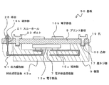
以下、図面を参照しながら、本発明の実施形態について説明する。図1、図2は、基板1を示す図であり、図1(a)は分解斜視図、図1(b)は組立斜視図、図2は基板1の断面図であって図1(b)のA−A線断面図である。基板1は、大電流で用いることが可能な基板である。 Hereinafter, embodiments of the present invention will be described with reference to the drawings. 1 and 2 are views showing the substrate 1, FIG. 1 (a) is an exploded perspective view, FIG. 1 (b) is an assembled perspective view, and FIG. 2 is a cross-sectional view of the substrate 1, and FIG. It is an AA line sectional view of). The substrate 1 is a substrate that can be used with a large current.
基板1は、射出成型基板3にプリント基板5が接続されて形成される。射出成型基板3には、電子部品搭載部7、プリント基板搭載部11が形成される。電子部品搭載部7、プリント基板搭載部11では、それぞれ内部の回路導体が、導体部15a、15bにおいて露出する。また、導体部以外の部位は樹脂9によって被覆される。
The substrate 1 is formed by connecting a printed
プリント基板5は、従来のガラスエポキシ基板を用いて構成する。プリント基板5には電子部品13bがあらかじめ搭載される。
The printed
電子部品搭載部7は、電子部品13aが搭載される部位である。また、プリント基板搭載部11は、プリント基板5が搭載される部位である。プリント基板5には、スルーホール21が設けられる。層間接続のためのスルーホール21にはメッキが施される。導体部15bはプリント基板搭載部11に略垂直に形成され、スルーホール21に挿入される。
The electronic component mounting part 7 is a part where the electronic component 13a is mounted. The printed board mounting portion 11 is a part on which the printed
プリント基板搭載部11の導体部15b近傍には、雌ネジ部17が形成される。雌ネジ部17は、固定部材であるボルト23と螺合可能である。電子部品13aは、電子部品搭載部7の導体部15aに半田等で接続される。また、プリント基板5は、導体部15bがスルーホール21を貫通して、プリント基板5上面において半田25で接続される。プリント基板5の半田5(スルーホール21)近傍には、あらかじめ孔19が形成される。ボルト23は、孔19を貫通して、雌ネジ部17に固定される。
A female screw portion 17 is formed in the vicinity of the conductor portion 15 b of the printed circuit board mounting portion 11. The female screw portion 17 can be screwed with a bolt 23 that is a fixing member. The electronic component 13a is connected to the conductor portion 15a of the electronic component mounting portion 7 with solder or the like. The printed
なお、本発明の基板としては、図示したような形状の基板に限られず、トランスやチョークコイルを有するDC−DCコンバータなど、大電流が流れる基板に対しては、当然に適用可能である。すなわち、本発明は、図に示すような部品配置および形状に限られることはなく、その他の部品等を適宜搭載することや、配置および形状を適宜変更することが可能なことは言うまでもない。 Note that the substrate of the present invention is not limited to the substrate having the shape shown in the figure, and can naturally be applied to a substrate through which a large current flows, such as a DC-DC converter having a transformer and a choke coil. That is, the present invention is not limited to the component arrangement and shape as shown in the drawings, and it goes without saying that other components and the like can be appropriately mounted, and the arrangement and shape can be appropriately changed.
図3は、図2のB部拡大図である。ボルト23の中心線と半田25(スルーホール21)の中心との距離をLとする。また、ボルト23の頭部の径をD(mm)とし、電気的な接合部である半田25の径(スルーホール21における導体パッドの径)をd(mm)とする。
FIG. 3 is an enlarged view of a portion B in FIG. Let L be the distance between the center line of the bolt 23 and the center of the solder 25 (through hole 21). The diameter of the head of the bolt 23 is D (mm), and the diameter of the
この場合、Lは、(D+d)/2+1mm以上であり、(D+d)/2+9mm以下であることが望ましい。Lが(D+d)/2+1mm以上であれば、固定部材と半田部とが干渉することがない。また、Lが(D+d)/2+9mmを超えると、急激に半田部へ付与される応力が増大する。したがって、Lを(D+d)/2+9mm以下とすることで、射出成型基板3とプリント基板5を構成するそれぞれの樹脂の熱膨張係数の違いにより、半田25に生じる応力を低減することができる。
In this case, L is preferably (D + d) / 2 + 1 mm or more and preferably (D + d) / 2 + 9 mm or less. When L is (D + d) / 2 + 1 mm or more, the fixing member and the solder portion do not interfere with each other. Further, when L exceeds (D + d) / 2 + 9 mm, the stress applied to the solder portion suddenly increases. Therefore, by setting L to (D + d) / 2 + 9 mm or less, the stress generated in the
図4は、ボルト23と半田25との中心距離Lと、半田25に付与される応力σとの関係を解析した図である。ボルトの頭部径を10mmΦ、スルーホール導体パットを4mmΦとして、それぞれの中心間距離Lを変えたときに、半田25にかかる最大応力をFEMで解析した。応力は、プリント基板の熱膨張係数を15ppm/℃(ガラスエポキシ基板FR−4に相当)とし、射出成型基板の熱膨張係数を40ppm/℃(ポリフェニレンサルファイドに相当)として、−40℃〜120℃まで温度を変化させた際の最大応力を算出した。
FIG. 4 is an analysis of the relationship between the center distance L between the bolt 23 and the
図4より明らかなように、Lが16mmを超えると急激に応力が増加する。したがって、本発明では、Lを16mm以下とすることが望ましい。すなわち、ボルト23の頭部の径をD(mm)とし、スルーホール21における導体パッドの径)をd(mm)とすると、(D+d)/2+9mmとすることが望ましい。 As is clear from FIG. 4, when L exceeds 16 mm, the stress rapidly increases. Therefore, in the present invention, it is desirable that L is 16 mm or less. That is, if the head diameter of the bolt 23 is D (mm) and the diameter of the conductor pad in the through hole 21 is d (mm), it is desirable to set (D + d) / 2 + 9 mm.
基板1は例えば以下のように製造される。まず、銅板等の導体である回路素材をプレスにより打ち抜き、必要な曲げ加工を施して所望の形状に形成する。銅板等には、必要に応じてSnメッキ等を施してもよい。次いで、複数の回路素材同士を溶接、または絶縁部材等を介して接合して回路導体を形成する。回路導体は、平面のみではなく、複数層に層状に形成されてもよい。 The substrate 1 is manufactured as follows, for example. First, a circuit material, which is a conductor such as a copper plate, is punched out by pressing, and necessary bending is performed to form a desired shape. You may give Sn plating etc. to a copper plate etc. as needed. Next, a plurality of circuit materials are welded or joined together via an insulating member or the like to form a circuit conductor. The circuit conductor may be formed not only in a plane but also in a plurality of layers.
得られた回路導体を所定位置にピン等で射出成型金型に固定し、樹脂を射出して射出成型を行う。この際、必要な導体露出部以外の部位が樹脂9により被覆され、また、回路素材同士の層間等にも樹脂が射出される。このようにして射出成型基板3が形成される。なお、雌ネジ部を構成する金属ナット等をあらかじめ設置して、射出時に樹脂で一体化してもよい。 The obtained circuit conductor is fixed at a predetermined position to the injection mold with a pin or the like, and resin is injected to perform injection molding. At this time, portions other than the necessary conductor exposed portions are covered with the resin 9, and the resin is also injected into the interlayer between the circuit materials. In this way, the injection molded substrate 3 is formed. A metal nut or the like constituting the female screw portion may be installed in advance and integrated with resin at the time of injection.
樹脂9としては、絶縁性があり、射出成型が可能であればよく、例えば、液晶ポリマー、ポリフェニレンサルファイド、ポリブチレンテレフタレート、ポリエーテルサルフォン、ポリエーテルエーテルケトン、ポリフタルアミド等が使用できる。 The resin 9 is only required to be insulative and injection-moldable. For example, liquid crystal polymer, polyphenylene sulfide, polybutylene terephthalate, polyether sulfone, polyether ether ketone, polyphthalamide and the like can be used.
なお、導体回路素材としては、例えば400μm以上の厚さの銅板等が用いられる。400μm未満では、大電流に耐えることが難しく、また、射出成型時の樹脂圧によって変形等の恐れがあるためである。なお、導体回路素材の厚さとしてさらに望ましくは、400μm〜1000μmである。厚すぎると、コスト及び重量等が増加し、コンパクトな基板を形成することができなくなるためである。 As the conductor circuit material, for example, a copper plate having a thickness of 400 μm or more is used. If it is less than 400 μm, it is difficult to withstand a large current, and there is a risk of deformation due to the resin pressure during injection molding. The thickness of the conductor circuit material is more preferably 400 μm to 1000 μm. If it is too thick, the cost and weight increase, and it becomes impossible to form a compact substrate.
次に、電子搭載部7に電子部品13aを搭載し、電子部品の電極を導体部15a等に電気的に接続する。同様に、プリント基板搭載部11には、プリント基板5を搭載し、プリント基板5のスルーホール21に導体部15bを挿入して電気的に接続する。それぞれの電気的な接続は、例えば半田、ワイヤーボンディング等を用いればよい。最後に、プリント基板5をボルト23で固定する。
Next, the electronic component 13a is mounted on the electronic mounting portion 7, and the electrodes of the electronic component are electrically connected to the conductor portion 15a and the like. Similarly, the printed circuit board mounting portion 11 is mounted with the printed
なお、プリント基板5上への部品の搭載は、所定位置にクリーム状の半田を印刷し、小型コンデンサ等の部品を所定位置に設置した後、リフロー炉を通して半田を溶融して接合をすればよい。
For mounting the components on the printed
以上説明したように、本実施形態の基板1によれば、回路素材をプレスで形成するため、厚銅基板を形成することができ、さらに樹脂9を射出成型により形成するため、製造性に優れ、大電流にも耐えうる基板1を得ることができる。このようにしてなる基板1では、信号系の小電流はプリント基板5上の回路(小型コンデンサ等)を利用するとともに、パワー系の大電流は射出成型基板の回路導体を利用することができる。したがって、1枚の基板上にこれら回路を全て搭載できるため、基板同士のケーブル等による接続が不要となり、低コストおよび小型化が達成できる。
As described above, according to the substrate 1 of the present embodiment, since the circuit material is formed by pressing, a thick copper substrate can be formed, and furthermore, the resin 9 is formed by injection molding. The substrate 1 that can withstand a large current can be obtained. In the substrate 1 thus configured, a signal system small current can use a circuit (such as a small capacitor) on the printed
また、プリント基板5と射出成型基板3とが半田25で接続され、半田25の近傍においてボルト23で固定されるため、半田25に過剰な応力が生じることがない。
Further, since the printed
また、スルーホール21に導体部15bを挿入して半田25で接続するため、半田部を容易に視認することができる。
Further, since the conductor portion 15b is inserted into the through hole 21 and connected with the
次に、第2の実施の形態について説明する。図5は、第2の実施の形態にかかる基板30を示す図である。なお、以下の説明において、基板1と同様の機能を奏する構成については、図1等と同様の符号を付し、重複する説明を省略する。
Next, a second embodiment will be described. FIG. 5 is a diagram illustrating a
基板30は、基板1と略同様の構成であるが、射出成型基板31等の態様が異なる。射出成型基板31には、一対の凸部33a、33bが形成される。凸部33a、33bは、射出成型基板31におけるプリント基板搭載部として機能する。
The
射出成型基板31より露出する導体部15bは、当該凸部33a、33b上面に露出する。プリント基板5は、少なくとも一対の凸部33a、33bにまたがるように設置される。導体部15bは、プリント基板5のスルーホール21を貫通し、半田25によりプリント基板5と電気的に接続される。
The conductor portion 15b exposed from the injection-molded substrate 31 is exposed on the upper surfaces of the convex portions 33a and 33b. The printed
凸部33bには、雌ネジ部17が設けられる。したがって、凸部33bにおいて、プリント基板5は、ボルト23によって射出成型基板31に固定される。また、凸部33aには、雌ネジ部17および導体部15bが露出する。凸部33a上には、プリント基板5のスルーホール21が配置される。したがって、凸部33aにおいて、プリント基板5は、導体部15bと電気的に接続されるとともに、ボルト23によって射出成型基板31に固定される。なお、凸部33a、33bの両者に、雌ネジ部17、導体部15bを露出させてもよい。また、以下の説明では、凸部33a、33bを合わせて凸部33と称する。
The female screw part 17 is provided in the convex part 33b. Therefore, the printed
なお、基板30においては、凸部33で挟まれた部位において、プリント基板5と射出成型基板31との間に空間が形成される。射出成型基板31に搭載される電子部品13aは、当該空間に配置されてもよい。すなわち、電子部品搭載部7は、凸部33の間に形成される。
In the
第2の実施の形態によれば、第1の実施の形態と同様の効果を得ることができる。また、射出成型基板上に搭載される電子部品とプリント基板に搭載される電子部品を層状に配置することができるため、小型な基板を得ることができる。 According to the second embodiment, an effect similar to that of the first embodiment can be obtained. Moreover, since the electronic component mounted on the injection-molded substrate and the electronic component mounted on the printed circuit board can be arranged in layers, a small substrate can be obtained.
次に、第3の実施の形態について説明する。図6(a)は、第3の実施の形態にかかる基板40aを示す図である。基板40aは、基板30に対して、さらに応力緩和部41が形成される。
Next, a third embodiment will be described. FIG. 6A shows a substrate 40a according to the third embodiment. The substrate 40 a further has a stress relaxation portion 41 formed on the
基板40aでは、プリント基板5と接続される導体部15bが、樹脂9の表面からまっすぐにはプリント基板5に貫通しない。導体部15bは、射出成型基板43aの側面から側方に向かって略水平(基板の面に略平行)に突出し、さらに屈曲されて上方に向けて形成される。屈曲部においては、少なくとも一部に、水平部および鉛直部が形成されることが望ましい。
In the board 40 a, the conductor portion 15 b connected to the printed
導体部15bの屈曲部が応力緩和部41として機能する。応力緩和部41は、プリント基板5と射出成型基板43aとの間の熱膨張差に伴う変形に対し、導体部15bが拘束されず、一部が変形可能である。このため、半田25に対して応力が発生することを緩和することができる。
The bent portion of the conductor portion 15 b functions as the stress relaxation portion 41. The stress relieving portion 41 can be partially deformed without being constrained by the conductor portion 15b with respect to deformation due to a difference in thermal expansion between the printed
応力緩和部41として、水平方向および鉛直方向の少なくとも2方向の部位が形成されれば、半田に生じる水平方向および鉛直方向の応力を容易に緩和することができる。 If at least two portions in the horizontal direction and the vertical direction are formed as the stress relaxation portion 41, the stress in the horizontal direction and the vertical direction generated in the solder can be easily relaxed.
なお、応力緩和部41の構成は、図6(a)の例には限られない。例えば、図6(b)に示す基板40bのように、応力緩和部41が射出成型基板43bの側面に露出する必要はない。すなわち、応力緩和部41は、プリント基板5との接続部と射出成型基板表面からの露出部との間に、導体部15bが拘束されずに変形可能な部位が形成されれば良い。
In addition, the structure of the stress relaxation part 41 is not restricted to the example of Fig.6 (a). For example, unlike the substrate 40b shown in FIG. 6B, the stress relaxation portion 41 does not need to be exposed on the side surface of the injection molded substrate 43b. That is, the stress relieving part 41 may be formed between the connecting part with the printed
図7は、応力緩和部のさらに変形例を示す図である。図7に示す基板50は、基板40aと略同様の構成であるが、導体部15bに屈曲部が形成される代わりに、細径部が形成される。すなわち、導体部15bの非拘束部において、他の部位よりも低剛性部が設けられる。低剛性部は他の部位よりも容易に変形可能である。このため、前述したような、プリント基板と射出成型基板との間の変位に対しても、当該応力緩和部が容易に変形して、半田25に付与される応力を緩和することができる。
FIG. 7 is a diagram showing a further modification of the stress relaxation portion. The substrate 50 shown in FIG. 7 has substantially the same configuration as the substrate 40a, but instead of forming a bent portion in the conductor portion 15b, a small diameter portion is formed. That is, in the non-restraining portion of the conductor portion 15b, a lower rigidity portion is provided than other portions. The low-rigidity part can be deformed more easily than other parts. For this reason, even when the displacement between the printed board and the injection-molded board is as described above, the stress relaxation portion is easily deformed, and the stress applied to the
第3の実施の形態によれば、第1の実施の形態と同様の効果を得ることができる。また、プリント基板と射出成型基板とを接続する導体部15bの一部が、射出成型基板の樹脂から露出して応力緩和部を構成するため、半田25に付与される応力を緩和することができる。
According to the third embodiment, an effect similar to that of the first embodiment can be obtained. Further, since a part of the conductor portion 15b connecting the printed circuit board and the injection molded substrate is exposed from the resin of the injection molded substrate to form a stress relaxation portion, the stress applied to the
以上、添付図を参照しながら、本発明の実施の形態を説明したが、本発明の技術的範囲は、前述した実施の形態に左右されない。当業者であれば、特許請求の範囲に記載された技術的思想の範疇内において各種の変更例または修正例に想到し得ることは明らかであり、それらについても当然に本発明の技術的範囲に属するものと了解される。 As mentioned above, although embodiment of this invention was described referring an accompanying drawing, the technical scope of this invention is not influenced by embodiment mentioned above. It is obvious for those skilled in the art that various modifications or modifications can be conceived within the scope of the technical idea described in the claims, and these are naturally within the technical scope of the present invention. It is understood that it belongs.
たとえば、上述した各構成は、当然にそれぞれ組み合わせることができる。また、プリント基板と射出成型基板との接続は、スルーホールを用いなくてもよい。また、ボルトに代えて、機械的に固定可能なピン等の固定部材を用いて、プリント基板と射出成型基板とを固定してもよい。 For example, the above-described configurations can be naturally combined. Further, the connection between the printed board and the injection molded board may not use a through hole. Further, the printed circuit board and the injection-molded circuit board may be fixed using a fixing member such as a mechanically fixable pin instead of the bolt.
1、30、40a、40b、50………基板
3………射出成型基板
5………プリント基板
7………電子部品搭載部
9………樹脂
11………プリント基板搭載部
13a、13b………電子部品
15a、15b………導体部
17………雌ネジ部
19………孔
21………スルーホール
23………ボルト
25………半田
31………射出成型基板
33a、33b………凸部
41、51………応力緩和部
43a、43b………射出成型基板
1, 30, 40 a, 40 b, 50... Substrate 3... Injection molded
Claims (10)
あらかじめ表面に電子部品が搭載されたプリント基板と、
を具備し、
前記射出成型基板からは、前記回路導体の一部が露出し、
露出した前記回路導体の一部が前記プリント基板と半田で電気的に接続され、
前記半田とは干渉しない前記半田とは異なる位置の前記半田の近傍で前記プリント基板が前記射出成型基板と固定部材で固定されることを特徴とする基板。 An injection-molded substrate in which resin is injection-molded on the surface of the circuit conductor;
A printed circuit board with electronic components mounted on the surface in advance,
Comprising
From the injection molded substrate, a part of the circuit conductor is exposed,
A portion of the exposed circuit conductor is electrically connected to the printed circuit board with solder;
A board characterized in that the printed board is fixed to the injection-molded board and a fixing member in the vicinity of the solder at a position different from the solder that does not interfere with the solder .
あらかじめ射出成型基板の樹脂部には雌ネジ部が形成されており、
前記ボルトを前記雌ネジ部に固定することで、前記プリント基板が固定されることを特徴とする請求項1記載の基板。 The fixing member is a bolt;
A female screw part is formed in advance on the resin part of the injection-molded substrate,
The board according to claim 1, wherein the printed board is fixed by fixing the bolt to the female screw portion.
前記凸部上に前記プリント基板が配置され、
前記固定部材であるボルトが、前記凸部に形成された雌ネジ部に固定されることを特徴とする請求項1から請求項4のいずれかに記載の基板。 The injection molded substrate is formed with at least a pair of convex portions,
The printed circuit board is disposed on the convex portion,
The board according to any one of claims 1 to 4, wherein a bolt as the fixing member is fixed to a female screw portion formed on the convex portion.
前記凸部上に配置された前記プリント基板のスルーホールに、露出した前記回路導体が貫通して、前記プリント基板と半田で電気的に接続されることを特徴とする請求項5記載の基板。 The circuit conductor is exposed on the convex portion,
The board according to claim 5, wherein the exposed circuit conductor penetrates through a through hole of the printed board disposed on the convex portion and is electrically connected to the printed board with solder.
前記空間において、前記射出成型基板上に電子部品が設置されることを特徴とする請求項5または請求項6記載の基板。 A space is formed between the injection molded board and the printed board,
The substrate according to claim 5 or 6, wherein an electronic component is installed on the injection-molded substrate in the space.
前記回路導体の表面に対して樹脂を射出成型して射出成型基板を成型し、
前記射出成型基板の上面に露出する回路導体の一部が、プリント基板のスルーホールを貫通するように前記プリント基板を設置し、
前記回路導体と、前記プリント基板および電子部品とを、半田で電気的に接続し、
あらかじめ前記射出成型基板の樹脂部に形成された雌ネジ部を用い、前記プリント基板を前記射出成型基板にボルトで固定することを特徴とする基板の製造方法。
Joining circuit materials that are conductors to form circuit conductors,
Injection molding a resin on the surface of the circuit conductor to mold an injection molding substrate,
Place the printed circuit board so that a part of the circuit conductor exposed on the upper surface of the injection molded circuit board penetrates the through hole of the printed circuit board,
The circuit conductor, the printed circuit board and the electronic component are electrically connected with solder,
A method for manufacturing a substrate, comprising: using a female screw portion previously formed in a resin portion of the injection molded substrate, and fixing the printed circuit board to the injection molded substrate with a bolt.
Priority Applications (5)
| Application Number | Priority Date | Filing Date | Title |
|---|---|---|---|
| JP2011051166A JP5449237B2 (en) | 2011-03-09 | 2011-03-09 | Substrate and substrate manufacturing method |
| EP12754301.5A EP2685795A4 (en) | 2011-03-09 | 2012-02-27 | Circuit board and method for manufacturing circuit board |
| CN2012800085530A CN103380662A (en) | 2011-03-09 | 2012-02-27 | Circuit board and method for manufacturing circuit board |
| PCT/JP2012/054711 WO2012121036A1 (en) | 2011-03-09 | 2012-02-27 | Circuit board and method for manufacturing circuit board |
| US14/021,053 US20140008105A1 (en) | 2011-03-09 | 2013-09-09 | Circuit board and method for manufacturing circuit board |
Applications Claiming Priority (1)
| Application Number | Priority Date | Filing Date | Title |
|---|---|---|---|
| JP2011051166A JP5449237B2 (en) | 2011-03-09 | 2011-03-09 | Substrate and substrate manufacturing method |
Publications (2)
| Publication Number | Publication Date |
|---|---|
| JP2012190883A JP2012190883A (en) | 2012-10-04 |
| JP5449237B2 true JP5449237B2 (en) | 2014-03-19 |
Family
ID=46798004
Family Applications (1)
| Application Number | Title | Priority Date | Filing Date |
|---|---|---|---|
| JP2011051166A Active JP5449237B2 (en) | 2011-03-09 | 2011-03-09 | Substrate and substrate manufacturing method |
Country Status (5)
| Country | Link |
|---|---|
| US (1) | US20140008105A1 (en) |
| EP (1) | EP2685795A4 (en) |
| JP (1) | JP5449237B2 (en) |
| CN (1) | CN103380662A (en) |
| WO (1) | WO2012121036A1 (en) |
Families Citing this family (5)
| Publication number | Priority date | Publication date | Assignee | Title |
|---|---|---|---|---|
| EP3072370B1 (en) * | 2013-11-21 | 2017-10-18 | ZF Friedrichshafen AG | Multifunctional printed circuit board |
| CN104078211B (en) * | 2014-06-12 | 2016-06-08 | 国网江苏省电力公司淮安供电公司 | The pole coil mounting board structure of transformer |
| CN104078210B (en) * | 2014-06-12 | 2016-06-08 | 国网江苏省电力公司淮安供电公司 | The method of installation base plate fixed magnetic pole coil |
| CN106028649B (en) * | 2016-07-28 | 2019-02-12 | Oppo广东移动通信有限公司 | The circuit board of mobile terminal and mobile terminal with it |
| KR102554299B1 (en) * | 2016-10-07 | 2023-07-12 | 한국전력공사 | Embeddfe 3d electronic circuit component, and manufacturing method thereof |
Family Cites Families (21)
| Publication number | Priority date | Publication date | Assignee | Title |
|---|---|---|---|---|
| US4630174A (en) * | 1983-10-31 | 1986-12-16 | Kaufman Lance R | Circuit package with external circuit board and connection |
| JPH0312233U (en) * | 1989-06-20 | 1991-02-07 | ||
| JPH0334703A (en) * | 1989-06-30 | 1991-02-14 | Nec Corp | Pattern connector between boards |
| JPH066529Y2 (en) * | 1990-02-02 | 1994-02-16 | 守 水沢 | Printed board for control panel |
| JPH06275328A (en) * | 1993-03-19 | 1994-09-30 | Fuji Elelctrochem Co Ltd | Printed board lead terminal and its mounting method |
| JPH0846317A (en) * | 1994-07-26 | 1996-02-16 | Honda Motor Co Ltd | Control board |
| JPH0936513A (en) * | 1995-07-20 | 1997-02-07 | Japan Aviation Electron Ind Ltd | Printed circuit device |
| JPH09121079A (en) * | 1995-10-26 | 1997-05-06 | Fujitsu Ten Ltd | Composite board structure |
| JPH10290054A (en) * | 1997-04-16 | 1998-10-27 | Sony Corp | Printed-wiring board |
| JPH11225459A (en) * | 1998-02-05 | 1999-08-17 | Matsushita Electric Ind Co Ltd | Motor controller |
| JP2000133897A (en) * | 1998-10-27 | 2000-05-12 | Matsushita Electric Ind Co Ltd | Resin-forming substrate |
| JP3538045B2 (en) * | 1998-12-09 | 2004-06-14 | 三菱電機株式会社 | RF circuit module |
| GB9911905D0 (en) * | 1999-05-22 | 1999-07-21 | Trw Lucas Varity Electric | Improvement relating to electrical power assisted steering |
| JP4510975B2 (en) * | 2000-02-08 | 2010-07-28 | パナソニック株式会社 | Circuit board |
| JP4026044B2 (en) * | 2000-05-09 | 2007-12-26 | 株式会社デンソー | Board connection member |
| JP4551552B2 (en) | 2000-10-24 | 2010-09-29 | 米沢電線株式会社 | Composite circuit board |
| JP2002368017A (en) * | 2001-06-05 | 2002-12-20 | Nikon Corp | Mounting board |
| JP4193650B2 (en) * | 2003-09-18 | 2008-12-10 | 株式会社デンソー | Circuit board |
| JP2009094457A (en) * | 2007-09-18 | 2009-04-30 | Olympus Corp | Laminated mounting structure and production process of laminated mounting structure |
| US7800222B2 (en) * | 2007-11-29 | 2010-09-21 | Infineon Technologies Ag | Semiconductor module with switching components and driver electronics |
| EP2120263A4 (en) * | 2007-11-30 | 2010-10-13 | Panasonic Corp | Heat dissipating structure base board, module using heat dissipating structure base board, and method for manufacturing heat dissipating structure base board |
-
2011
- 2011-03-09 JP JP2011051166A patent/JP5449237B2/en active Active
-
2012
- 2012-02-27 EP EP12754301.5A patent/EP2685795A4/en not_active Withdrawn
- 2012-02-27 CN CN2012800085530A patent/CN103380662A/en active Pending
- 2012-02-27 WO PCT/JP2012/054711 patent/WO2012121036A1/en unknown
-
2013
- 2013-09-09 US US14/021,053 patent/US20140008105A1/en not_active Abandoned
Also Published As
| Publication number | Publication date |
|---|---|
| WO2012121036A1 (en) | 2012-09-13 |
| JP2012190883A (en) | 2012-10-04 |
| EP2685795A1 (en) | 2014-01-15 |
| CN103380662A (en) | 2013-10-30 |
| EP2685795A4 (en) | 2015-03-25 |
| US20140008105A1 (en) | 2014-01-09 |
Similar Documents
| Publication | Publication Date | Title |
|---|---|---|
| US7267556B2 (en) | Electrical junction box | |
| WO2011129130A1 (en) | Board and method for manufacturing board | |
| JP5449237B2 (en) | Substrate and substrate manufacturing method | |
| JP5100694B2 (en) | Semiconductor device | |
| JP5697020B2 (en) | Substrate and substrate manufacturing method | |
| US9368309B2 (en) | Electronic part and electronic control unit | |
| US11439005B2 (en) | Inductor bridge and electronic device | |
| JP5004337B2 (en) | External connection terminal of metal core board | |
| CN100562216C (en) | The heat abstractor that is used for electric equipment | |
| JP2007281138A (en) | Wiring board | |
| JP6280261B1 (en) | Connection structure for electronic components and circuit boards | |
| JP5376209B2 (en) | Circuit structure | |
| JP4728873B2 (en) | Wiring board unit | |
| JP5063672B2 (en) | Wiring board and manufacturing method thereof | |
| JP5255592B2 (en) | substrate | |
| JP5415858B2 (en) | Thick conductor substrate and manufacturing method thereof | |
| JP3685046B2 (en) | Junction box | |
| JP6376467B2 (en) | Busbar circuit body | |
| WO2023195195A1 (en) | Power conversion device | |
| US9437992B2 (en) | Busbar | |
| JP4914247B2 (en) | Electronic control device | |
| JP2010212642A (en) | Printed wiring board | |
| JP5445470B2 (en) | Board to board connection structure | |
| JP4297318B2 (en) | Circuit board and electrical junction box | |
| JP2009147223A (en) | Module part, module and method of manufacturing module part |
Legal Events
| Date | Code | Title | Description |
|---|---|---|---|
| A621 | Written request for application examination |
Free format text: JAPANESE INTERMEDIATE CODE: A621 Effective date: 20120702 |
|
| A131 | Notification of reasons for refusal |
Free format text: JAPANESE INTERMEDIATE CODE: A131 Effective date: 20130507 |
|
| A521 | Written amendment |
Free format text: JAPANESE INTERMEDIATE CODE: A523 Effective date: 20130618 |
|
| TRDD | Decision of grant or rejection written | ||
| A01 | Written decision to grant a patent or to grant a registration (utility model) |
Free format text: JAPANESE INTERMEDIATE CODE: A01 Effective date: 20131126 |
|
| A61 | First payment of annual fees (during grant procedure) |
Free format text: JAPANESE INTERMEDIATE CODE: A61 Effective date: 20131224 |
|
| R151 | Written notification of patent or utility model registration |
Ref document number: 5449237 Country of ref document: JP Free format text: JAPANESE INTERMEDIATE CODE: R151 |
|
| S531 | Written request for registration of change of domicile |
Free format text: JAPANESE INTERMEDIATE CODE: R313531 |
|
| R350 | Written notification of registration of transfer |
Free format text: JAPANESE INTERMEDIATE CODE: R350 |