JP4891682B2 - Liquid crystal display device and driving method thereof - Google Patents
Liquid crystal display device and driving method thereof Download PDFInfo
- Publication number
- JP4891682B2 JP4891682B2 JP2006195304A JP2006195304A JP4891682B2 JP 4891682 B2 JP4891682 B2 JP 4891682B2 JP 2006195304 A JP2006195304 A JP 2006195304A JP 2006195304 A JP2006195304 A JP 2006195304A JP 4891682 B2 JP4891682 B2 JP 4891682B2
- Authority
- JP
- Japan
- Prior art keywords
- data
- voltage
- pixel
- liquid crystal
- gate
- Prior art date
- Legal status (The legal status is an assumption and is not a legal conclusion. Google has not performed a legal analysis and makes no representation as to the accuracy of the status listed.)
- Expired - Fee Related
Links
Images


Classifications
-
- G—PHYSICS
- G09—EDUCATION; CRYPTOGRAPHY; DISPLAY; ADVERTISING; SEALS
- G09G—ARRANGEMENTS OR CIRCUITS FOR CONTROL OF INDICATING DEVICES USING STATIC MEANS TO PRESENT VARIABLE INFORMATION
- G09G3/00—Control arrangements or circuits, of interest only in connection with visual indicators other than cathode-ray tubes
- G09G3/20—Control arrangements or circuits, of interest only in connection with visual indicators other than cathode-ray tubes for presentation of an assembly of a number of characters, e.g. a page, by composing the assembly by combination of individual elements arranged in a matrix no fixed position being assigned to or needed to be assigned to the individual characters or partial characters
- G09G3/34—Control arrangements or circuits, of interest only in connection with visual indicators other than cathode-ray tubes for presentation of an assembly of a number of characters, e.g. a page, by composing the assembly by combination of individual elements arranged in a matrix no fixed position being assigned to or needed to be assigned to the individual characters or partial characters by control of light from an independent source
- G09G3/36—Control arrangements or circuits, of interest only in connection with visual indicators other than cathode-ray tubes for presentation of an assembly of a number of characters, e.g. a page, by composing the assembly by combination of individual elements arranged in a matrix no fixed position being assigned to or needed to be assigned to the individual characters or partial characters by control of light from an independent source using liquid crystals
- G09G3/3611—Control of matrices with row and column drivers
- G09G3/3685—Details of drivers for data electrodes
- G09G3/3688—Details of drivers for data electrodes suitable for active matrices only
-
- G—PHYSICS
- G09—EDUCATION; CRYPTOGRAPHY; DISPLAY; ADVERTISING; SEALS
- G09G—ARRANGEMENTS OR CIRCUITS FOR CONTROL OF INDICATING DEVICES USING STATIC MEANS TO PRESENT VARIABLE INFORMATION
- G09G3/00—Control arrangements or circuits, of interest only in connection with visual indicators other than cathode-ray tubes
- G09G3/20—Control arrangements or circuits, of interest only in connection with visual indicators other than cathode-ray tubes for presentation of an assembly of a number of characters, e.g. a page, by composing the assembly by combination of individual elements arranged in a matrix no fixed position being assigned to or needed to be assigned to the individual characters or partial characters
- G09G3/34—Control arrangements or circuits, of interest only in connection with visual indicators other than cathode-ray tubes for presentation of an assembly of a number of characters, e.g. a page, by composing the assembly by combination of individual elements arranged in a matrix no fixed position being assigned to or needed to be assigned to the individual characters or partial characters by control of light from an independent source
- G09G3/36—Control arrangements or circuits, of interest only in connection with visual indicators other than cathode-ray tubes for presentation of an assembly of a number of characters, e.g. a page, by composing the assembly by combination of individual elements arranged in a matrix no fixed position being assigned to or needed to be assigned to the individual characters or partial characters by control of light from an independent source using liquid crystals
-
- G—PHYSICS
- G09—EDUCATION; CRYPTOGRAPHY; DISPLAY; ADVERTISING; SEALS
- G09G—ARRANGEMENTS OR CIRCUITS FOR CONTROL OF INDICATING DEVICES USING STATIC MEANS TO PRESENT VARIABLE INFORMATION
- G09G3/00—Control arrangements or circuits, of interest only in connection with visual indicators other than cathode-ray tubes
- G09G3/20—Control arrangements or circuits, of interest only in connection with visual indicators other than cathode-ray tubes for presentation of an assembly of a number of characters, e.g. a page, by composing the assembly by combination of individual elements arranged in a matrix no fixed position being assigned to or needed to be assigned to the individual characters or partial characters
- G09G3/34—Control arrangements or circuits, of interest only in connection with visual indicators other than cathode-ray tubes for presentation of an assembly of a number of characters, e.g. a page, by composing the assembly by combination of individual elements arranged in a matrix no fixed position being assigned to or needed to be assigned to the individual characters or partial characters by control of light from an independent source
- G09G3/36—Control arrangements or circuits, of interest only in connection with visual indicators other than cathode-ray tubes for presentation of an assembly of a number of characters, e.g. a page, by composing the assembly by combination of individual elements arranged in a matrix no fixed position being assigned to or needed to be assigned to the individual characters or partial characters by control of light from an independent source using liquid crystals
- G09G3/3611—Control of matrices with row and column drivers
- G09G3/3648—Control of matrices with row and column drivers using an active matrix
- G09G3/3659—Control of matrices with row and column drivers using an active matrix the addressing of the pixel involving the control of two or more scan electrodes or two or more data electrodes, e.g. pixel voltage dependant on signal of two data electrodes
-
- G—PHYSICS
- G09—EDUCATION; CRYPTOGRAPHY; DISPLAY; ADVERTISING; SEALS
- G09G—ARRANGEMENTS OR CIRCUITS FOR CONTROL OF INDICATING DEVICES USING STATIC MEANS TO PRESENT VARIABLE INFORMATION
- G09G2300/00—Aspects of the constitution of display devices
- G09G2300/04—Structural and physical details of display devices
- G09G2300/0439—Pixel structures
- G09G2300/0443—Pixel structures with several sub-pixels for the same colour in a pixel, not specifically used to display gradations
- G09G2300/0447—Pixel structures with several sub-pixels for the same colour in a pixel, not specifically used to display gradations for multi-domain technique to improve the viewing angle in a liquid crystal display, such as multi-vertical alignment [MVA]
-
- G—PHYSICS
- G09—EDUCATION; CRYPTOGRAPHY; DISPLAY; ADVERTISING; SEALS
- G09G—ARRANGEMENTS OR CIRCUITS FOR CONTROL OF INDICATING DEVICES USING STATIC MEANS TO PRESENT VARIABLE INFORMATION
- G09G2300/00—Aspects of the constitution of display devices
- G09G2300/08—Active matrix structure, i.e. with use of active elements, inclusive of non-linear two terminal elements, in the pixels together with light emitting or modulating elements
- G09G2300/0876—Supplementary capacities in pixels having special driving circuits and electrodes instead of being connected to common electrode or ground; Use of additional capacitively coupled compensation electrodes
-
- G—PHYSICS
- G09—EDUCATION; CRYPTOGRAPHY; DISPLAY; ADVERTISING; SEALS
- G09G—ARRANGEMENTS OR CIRCUITS FOR CONTROL OF INDICATING DEVICES USING STATIC MEANS TO PRESENT VARIABLE INFORMATION
- G09G2310/00—Command of the display device
- G09G2310/02—Addressing, scanning or driving the display screen or processing steps related thereto
- G09G2310/0202—Addressing of scan or signal lines
- G09G2310/0205—Simultaneous scanning of several lines in flat panels
-
- G—PHYSICS
- G09—EDUCATION; CRYPTOGRAPHY; DISPLAY; ADVERTISING; SEALS
- G09G—ARRANGEMENTS OR CIRCUITS FOR CONTROL OF INDICATING DEVICES USING STATIC MEANS TO PRESENT VARIABLE INFORMATION
- G09G2310/00—Command of the display device
- G09G2310/02—Addressing, scanning or driving the display screen or processing steps related thereto
- G09G2310/0202—Addressing of scan or signal lines
- G09G2310/0213—Addressing of scan or signal lines controlling the sequence of the scanning lines with respect to the patterns to be displayed, e.g. to save power
-
- G—PHYSICS
- G09—EDUCATION; CRYPTOGRAPHY; DISPLAY; ADVERTISING; SEALS
- G09G—ARRANGEMENTS OR CIRCUITS FOR CONTROL OF INDICATING DEVICES USING STATIC MEANS TO PRESENT VARIABLE INFORMATION
- G09G2310/00—Command of the display device
- G09G2310/06—Details of flat display driving waveforms
- G09G2310/061—Details of flat display driving waveforms for resetting or blanking
-
- G—PHYSICS
- G09—EDUCATION; CRYPTOGRAPHY; DISPLAY; ADVERTISING; SEALS
- G09G—ARRANGEMENTS OR CIRCUITS FOR CONTROL OF INDICATING DEVICES USING STATIC MEANS TO PRESENT VARIABLE INFORMATION
- G09G2310/00—Command of the display device
- G09G2310/08—Details of timing specific for flat panels, other than clock recovery
-
- G—PHYSICS
- G09—EDUCATION; CRYPTOGRAPHY; DISPLAY; ADVERTISING; SEALS
- G09G—ARRANGEMENTS OR CIRCUITS FOR CONTROL OF INDICATING DEVICES USING STATIC MEANS TO PRESENT VARIABLE INFORMATION
- G09G2320/00—Control of display operating conditions
- G09G2320/02—Improving the quality of display appearance
- G09G2320/0247—Flicker reduction other than flicker reduction circuits used for single beam cathode-ray tubes
-
- G—PHYSICS
- G09—EDUCATION; CRYPTOGRAPHY; DISPLAY; ADVERTISING; SEALS
- G09G—ARRANGEMENTS OR CIRCUITS FOR CONTROL OF INDICATING DEVICES USING STATIC MEANS TO PRESENT VARIABLE INFORMATION
- G09G2320/00—Control of display operating conditions
- G09G2320/02—Improving the quality of display appearance
- G09G2320/0261—Improving the quality of display appearance in the context of movement of objects on the screen or movement of the observer relative to the screen
-
- G—PHYSICS
- G09—EDUCATION; CRYPTOGRAPHY; DISPLAY; ADVERTISING; SEALS
- G09G—ARRANGEMENTS OR CIRCUITS FOR CONTROL OF INDICATING DEVICES USING STATIC MEANS TO PRESENT VARIABLE INFORMATION
- G09G2320/00—Control of display operating conditions
- G09G2320/06—Adjustment of display parameters
- G09G2320/068—Adjustment of display parameters for control of viewing angle adjustment
Abstract
Description
本発明は液晶表示装置及びその駆動方法に関するものである。 The present invention relates to a liquid crystal display device and a driving method thereof.
液晶表示装置は現在最も広く使用されている平板表示装置のうちの1つであって、画素電極と共通電極など、電場生成電極が形成されている2枚の表示板と、その間に挿入されている液晶層からなり、電場生成電極に電圧を印加して液晶層に電場を生成し、これを通じて液晶層の液晶分子の配向を決めて入射光の偏光を制御することによって映像を表示する。 The liquid crystal display device is one of the most widely used flat panel display devices, and includes two display plates on which electric field generating electrodes such as a pixel electrode and a common electrode are formed, and inserted between them. An image is displayed by applying a voltage to the electric field generating electrode to generate an electric field in the liquid crystal layer, determining the orientation of the liquid crystal molecules in the liquid crystal layer, and controlling the polarization of incident light.
液晶表示装置の中でも電場が印加されない状態で液晶分子の長軸を上下表示板に対して垂直をなすように配列した垂直配向モード液晶表示装置はコントラスト比が大きくて広い基準視野角の実現が容易であるので注目されている。ここで、基準視野角とはコントラスト比が1:10である視野角または階調間輝度反転限界角度を意味する。
垂直配向モード液晶表示装置で広視野角を実現するための手段としては、電場生成電極に切開部を形成する方法と電場生成電極上に突起を形成する方法などがある。切開部と突起で液晶分子の傾斜方向を決めることができるので、これらを使用して液晶分子の傾斜方向を多様な方向に分散させることで基準視野角を広めることができる。
Among liquid crystal display devices, a vertical alignment mode liquid crystal display device in which the long axes of liquid crystal molecules are aligned perpendicularly to the upper and lower display plates without applying an electric field has a large contrast ratio and can easily realize a wide reference viewing angle. Therefore, it is attracting attention. Here, the reference viewing angle means a viewing angle having a contrast ratio of 1:10 or a luminance inversion limit angle between gradations.
As means for realizing a wide viewing angle in the vertical alignment mode liquid crystal display device, there are a method of forming an incision in the electric field generating electrode and a method of forming a protrusion on the electric field generating electrode. Since the tilt direction of the liquid crystal molecules can be determined by the incision and the protrusion, the reference viewing angle can be widened by using these to disperse the tilt direction of the liquid crystal molecules in various directions.
しかし、垂直配向モードの液晶表示装置は前面視認性に比べて側面視認性が落ちる。例えば、切開部が備えられたPVA(patterned vertically aligned)モードの液晶表示装置の場合には、側面へ行くほど映像が明るくなって、激しい場合には高い階調の間の輝度差がなくなって画面が崩れているように見える場合も発生する。
側面視認性を改善するために1つの画素を2つの副画素に分割し、2つの副画素を容量性結合させた後、一方の副画素には直接電圧を印加し、他方の副画素には容量性結合による電圧下降を起こして2つの副画素の電圧を異ならせることで透過率を異ならせる方法が提示された。
However, the liquid crystal display device in the vertical alignment mode has lower side visibility than front visibility. For example, in the case of a liquid crystal display device in PVA (patterned vertically aligned) mode with an incision, the image becomes brighter as it goes to the side. It may also occur when appears to be broken.
In order to improve the side visibility, one pixel is divided into two subpixels, and after the two subpixels are capacitively coupled, a voltage is directly applied to one subpixel and the other subpixel is applied to the other subpixel. A method has been proposed in which the transmittance is varied by causing a voltage drop due to capacitive coupling to vary the voltages of the two sub-pixels.
一方、液晶表示装置はホールドタイプ(hold type)の表示装置であるので、動映像を表示する時に物体の輪郭(edge)が鮮明でなくて薄くなるブラリング(blurring)現象が発生する。ブラリング現象をなくすために、表示しようとする正規映像を表示しながら、その中間にブラック映像を表示するインパルシブ(impulsive)駆動方式が開発された。しかし、インパルシブ駆動方式によれば、ブラック映像が表示されるので全体的に輝度が低下し、ブラック映像と正規映像の境界部分で画面が点灯するフリッカーが発生することがある。 On the other hand, since the liquid crystal display device is a hold type display device, a blurring phenomenon occurs in which an edge of an object is not clear and thin when displaying a moving image. In order to eliminate the blurring phenomenon, an impulsive drive system has been developed that displays a normal video to be displayed while displaying a black video in the middle. However, according to the impulsive driving method, since the black image is displayed, the luminance is lowered as a whole, and flicker may occur in which the screen is lit at the boundary between the black image and the regular image.
そこで、本発明が解決しようとする技術的課題は、輝度低下及びフリッカー発生を最小化しながら、ブラリング現象を防止し、側面視認性を向上させることができる液晶表示装置及びその駆動方法を提供することにある。 Therefore, a technical problem to be solved by the present invention is to provide a liquid crystal display device and a driving method thereof that can prevent a blurring phenomenon and improve side visibility while minimizing a decrease in luminance and occurrence of flicker. There is.
このような技術的課題を構成するための本発明の1つの実施例による液晶表示装置は、ゲートオン電圧を伝達する複数のゲート線、第1及び第2正規映像データ電圧とインパルシブデータ電圧を伝達する複数のデータ線、前記ゲート線及び前記データ線に接続されていて第1及び第2副画素電極を含む複数の画素、前記ゲート線に接続されて前記ゲートオン電圧を印加するゲート駆動部、そして前記データ線に接続されて前記第1及び第2正規映像データ電圧と前記インパルシブデータ電圧を印加するデータ駆動部を含み、前記第1副画素電極と前記第2副画素電極に各々印加される前記第1及び第2正規映像データ電圧は1つの映像情報から得られて互いに異なり、前記インパルシブデータ電圧は前記第1及び第2副画素電極のうちのいずれか1つに印加されるように構成する。 A liquid crystal display according to an embodiment of the present invention for constructing such a technical problem includes a plurality of gate lines for transmitting a gate-on voltage, first and second normal video data voltages, and an impulsive data voltage. A plurality of data lines, a plurality of pixels connected to the gate lines and the data lines and including first and second subpixel electrodes, a gate driver connected to the gate lines and applying the gate-on voltage, and A data driver connected to the data line and applying the first and second normal video data voltages and the impulsive data voltage, and is applied to the first subpixel electrode and the second subpixel electrode, respectively; The first and second normal video data voltages are obtained from one video information and are different from each other, and the impulsive data voltage is one of the first and second subpixel electrodes. Configured to either be applied to one.
前記第1正規映像データ電圧は前記第2正規映像データ電圧より大きく、前記第1副画素電極の面積は前記第2副画素電極の面積より小さくてもよい。
前記インパルシブデータ電圧は前記第2副画素電極に印加できる。
前記インパルシブデータ電圧は前記第1及び第2正規映像データ電圧より小さくてもよい。
The first normal video data voltage may be larger than the second normal video data voltage, and the area of the first subpixel electrode may be smaller than the area of the second subpixel electrode.
The impulsive data voltage may be applied to the second subpixel electrode.
The impulsive data voltage may be smaller than the first and second normal video data voltages.
前記インパルシブデータ電圧は最も低い階調の電圧、ブラックを表示する階調の電圧及び所定範囲の輝度を出す階調の電圧のうちのいずれか1つであってもよい。
M個の束の映像情報を受けて各M個の束の第1及び第2正規映像データに変換し、1つの束のインパルシブデータを生成して前記第1及び第2正規映像データ及び前記インパルシブデータを前記データ駆動部に伝送する信号制御部をさらに含むことができる。
The impulsive data voltage may be one of a lowest gradation voltage, a gradation voltage for displaying black, and a gradation voltage for producing a predetermined range of luminance.
M pieces of video information are received and converted into first and second regular video data of each of M bundles, one bundle of impulsive data is generated, and the first and second regular video data and the The apparatus may further include a signal controller that transmits impulsive data to the data driver.
前記第1正規映像データは前記第2正規映像データより大きく、前記インパルシブデータは前記第2正規映像データより小さくてもよい。
互いに異なる第1及び第2階調電圧集合を生成し、前記第1及び第2階調電圧集合から前記第1及び第2正規映像データ電圧を各々選択して、前記第1及び第2副画素電極に各々印加することができる。
The first regular video data may be larger than the second regular video data, and the impulsive data may be smaller than the second regular video data.
First and second sub-pixels are generated by generating different first and second grayscale voltage sets, selecting the first and second normal image data voltages from the first and second grayscale voltage sets, respectively. Each can be applied to an electrode.
前記第1及び第2副画素電極に各々接続されている第1及び第2スイッチング素子をさらに含み、前記ゲート線は前記第1及び第2スイッチング素子に各々接続されている第1及び第2ゲート線を含むことができる。
前記インパルシブデータ電圧は複数の画素行の第2副画素電極に同時に印加できる。
前記第1及び第2正規映像データ電圧は各々複数の画素行の第1及び第2副画素電極に交互であって順に印加することができる。
First and second switching elements connected to the first and second subpixel electrodes, respectively, and the gate line is connected to the first and second switching elements, respectively. Lines can be included.
The impulsive data voltage can be simultaneously applied to the second subpixel electrodes of a plurality of pixel rows.
The first and second normal image data voltages may be alternately applied to the first and second subpixel electrodes of a plurality of pixel rows, respectively.
第1番目M個の画素行の第1及び第2副画素電極に前記第1番目M個の画素行の第1及び第2正規映像データ電圧を交互であって順に各々印加した後、第2番目M個の画素行の第2副画素電極に前記インパルシブデータ電圧を同時に印加することができる。
前記第2番目M個の画素行の第2副画素電極に前記インパルシブデータ電圧を印加した後、前記第1番目M個の画素行の第1及び第2副画素電極に印加された前記第1及び第2正規映像データ電圧の極性と異なる所定の先充電電圧を前記データ線に印加することができる。
The first and second normal image data voltages of the first M pixel rows are alternately applied to the first and second sub-pixel electrodes of the first M pixel rows, respectively, and then second The impulsive data voltage may be simultaneously applied to the second subpixel electrode of the Mth pixel row.
The impulsive data voltage is applied to the second subpixel electrodes of the second M pixel rows, and then the first and second subpixel electrodes of the first M pixel rows are applied to the first subpixel electrodes. A predetermined precharge voltage different from the polarities of the first and second normal video data voltages can be applied to the data line.
前記データ駆動部は複数の出力端子を接続し、前記ゲート駆動部は前記第2ゲート線に前記ゲートオン電圧を印加することができる。
前記ゲート駆動部は複数の水平周期の間に前記第2ゲート線に前記ゲートオン電圧を複数回印加することができる。
前記ゲート駆動部は複数の画素行の第2ゲート線に前記ゲートオン電圧を同時に印加することができる。
The data driver may connect a plurality of output terminals, and the gate driver may apply the gate-on voltage to the second gate line.
The gate driver may apply the gate-on voltage to the second gate line a plurality of times during a plurality of horizontal periods.
The gate driver may simultaneously apply the gate-on voltage to the second gate lines of a plurality of pixel rows.
前記第1及び第2副画素電極に各々接続されている第1及び第2スイッチング素子をさらに含み、前記データ線は前記第1及び第2スイッチング素子に各々接続されている第1及び第2データ線を含むことができる。
第1番目画素行の第1及び第2副画素電極に前記第1番目画素行の第1及び第2正規映像データ電圧が各々印加された後、第2画素行の第1及び第2副画素電極に前記第2画素行の第1正規映像データ電圧及び前記インパルシブデータ電圧を各々印加することができる。
First and second switching elements connected to the first and second subpixel electrodes, respectively, and the data line is connected to the first and second switching elements, respectively. Lines can be included.
After the first and second normal image data voltages of the first pixel row are respectively applied to the first and second subpixel electrodes of the first pixel row, the first and second subpixels of the second pixel row The first normal video data voltage and the impulsive data voltage of the second pixel row may be applied to the electrodes, respectively.
本発明の他の特徴による第1及び第2副画素電極を含む複数の画素を含む液晶表示装置の駆動方法は、前記第1及び第2副画素電極に第1及び第2正規映像データ電圧を各々印加する段階、そして前記第1及び第2副画素電極のうちのいずれか1つにインパルシブデータ電圧を印加する段階を含み、前記第1及び第2正規映像データ電圧は1つの映像情報から得られるとともに互いに異なるように構成できる。 According to another aspect of the present invention, there is provided a driving method of a liquid crystal display device including a plurality of pixels including first and second subpixel electrodes, wherein the first and second normal image data voltages are applied to the first and second subpixel electrodes. Respectively, and applying an impulsive data voltage to any one of the first and second subpixel electrodes, wherein the first and second normal image data voltages are obtained from one image information. It can be obtained and different from each other.
本発明によれば、複数の画素行にインパルシブ映像を同時に表示することによってインパルシブ映像を表示するための駆動時間を相対的に減らすことができるので、画像電圧の充電率を高めることができ、その結果、充電率不足によるフリッカー発生を最小化することができる。また、インパルシブ映像を1つの副画素に表示し、他の副画素に正規映像を表示することによってブラリングを防止しながら、輝度低下を減らすことができる。 According to the present invention, it is possible to relatively reduce the driving time for displaying the impulsive image by simultaneously displaying the impulsive image on the plurality of pixel rows, so that the charging rate of the image voltage can be increased. As a result, occurrence of flicker due to insufficient charging rate can be minimized. Further, by displaying impulsive video on one sub-pixel and displaying regular video on the other sub-pixel, it is possible to reduce brightness reduction while preventing blurring.
添付した図面を参照して本発明の実施例について本発明の属する技術分野における通常の知識を有する者が容易に実施できるように詳細に説明する。
図面において多様な層及び領域を明確に表現するために厚さを拡大して示した。明細書全体にわたって類似する部分については同一図面符号を付けた。層、膜、領域、板などの部分が他の部分の“上”にあるとする時、これは他の部分の“直上”にある場合だけでなく、その中間に他の部分がある場合も含む。反対に、ある部分が他の部分の“直上”にあるとする時には中間に他の部分がないことを意味する。
Embodiments of the present invention will be described in detail with reference to the accompanying drawings so that those skilled in the art to which the present invention pertains can easily carry out the embodiments.
In the drawings, the thickness is enlarged to clearly show various layers and regions. Similar parts are denoted by the same reference numerals throughout the specification. When a layer, film, region, plate, etc. is “on” other parts, this is not only “directly above” other parts, but also other parts in the middle Including. On the other hand, when a part is “just above” another part, it means that there is no other part in the middle.
まず、図1及び図2を参照して本発明の1つの実施例による液晶表示装置について詳細に説明する。
図1は本発明の1つの実施例による液晶表示装置のブロック図であり、図2は本発明の1つの実施例による液晶表示装置の1つの画素に対する等価回路図である。
図1に示したように、本発明の1つの実施例による液晶表示装置は液晶表示板組立体300及び、これと接続されたゲート駆動部400及びデータ駆動部500、データ駆動部500に接続された階調電圧生成部800、そしてこれらを制御する信号制御部600を含む。
First, a liquid crystal display device according to an embodiment of the present invention will be described in detail with reference to FIGS.
FIG. 1 is a block diagram of a liquid crystal display device according to one embodiment of the present invention, and FIG. 2 is an equivalent circuit diagram for one pixel of the liquid crystal display device according to one embodiment of the present invention.
As shown in FIG. 1, a liquid crystal display according to an embodiment of the present invention is connected to a liquid
液晶表示板組立体300は等価回路で見る時、複数の信号線Gi、Dj(i=1,2,…,n、j=1,2,…,mと、これに接続されていてほぼ行列形態で配列された複数の画素PXを含む。これに反し、図2に示した構造で見る時、液晶表示板組立体300は互いに対向する下部及び上部表示板100、200と、その間に入っている液晶層3を含む。
信号線Gi、Djはゲート信号(“走査信号”とも言う)を伝達する複数のゲート線Giとデータ信号を伝達する複数のデータ線Djを含む。ゲート線はほぼ行方向に延びて互いにほぼ平行であり、データ線はほぼ列方向に延びて互いにほぼ平行である。
When viewed in an equivalent circuit, the liquid
The signal lines G i and D j include a plurality of gate lines G i for transmitting gate signals (also referred to as “scanning signals”) and a plurality of data lines D j for transmitting data signals. The gate lines extend in the row direction and are substantially parallel to each other, and the data lines extend in the column direction and are substantially parallel to each other.
各画素PXは信号線Gi、Djに接続されたスイッチング素子Qと、これに接続された液晶キャパシタCLC及びストレージキャパシタCSTを含む。ストレージキャパシタCSTは必要によって省略することができる。
スイッチング素子Qは下部表示板100に設けられている薄膜トランジスタなどの三端子素子であって、その制御端子はゲート線Giと接続されており、入力端子はデータ線Djと接続されており、出力端子は液晶キャパシタCLC及びストレージキャパシタCSTと接続されている。
Each pixel PX includes a signal line G i, a switching element Q connected to the D j, a liquid crystal capacitor C LC and the storage capacitor C ST that are connected thereto. The storage capacitor CST can be omitted if necessary.
The switching element Q is a three terminal element such as a thin film transistor provided on the
液晶キャパシタCLCは下部表示板100の画素電極191と上部表示板200の共通電極270を2つの端子とし、2つの電極191、270の間の液晶層3は誘電体として機能する。画素電極191はスイッチング素子Qと接続され、共通電極270は上部表示板200の前面に形成されていて共通電圧Vcomの印加を受ける。図2とは異なって、共通電極270を下部表示板100に設けることもでき、この時には2つの電極191、270のうちの少なくとも1つが線状または棒状に形成することもできる。
The liquid crystal capacitor C LC has the
液晶キャパシタCLCの補助的な役割を果たすストレージキャパシタCSTは、下部表示板100に設けられた別個の信号線(図示せず)と画素電極191が絶縁体を間に置いて重なってなり、この別個の信号線には共通電圧Vcomなどの決められた電圧が印加される。しかし、ストレージキャパシタCSTは画素電極191が絶縁体を媒介として直上の前段ゲート線と重なって構成されてもよい。
The liquid crystal capacitor C plays an auxiliary role storage capacitor C ST of the LC is a separate signal line provided on the lower panel 100 (not shown) and the
一方、色表示を実現するためには各画素PXが基本色のうちの1つを固有に表示したり(空間分割)、各画素PXが時間によって交互に基本色を表示したり(時間分割)して、これら基本色の空間的、時間的合計で所望する色相を認識させる。基本色の例としては、赤色、緑色、青色などの三原色がある。図2は空間分割の一例で、各画素PXが画素電極191に対応する上部表示板200の領域に基本色のうちの1つを示す色フィルター230を備えることを示している。図2とは異なって、色フィルター230は下部表示板100の画素電極191の上または下に形成してもよい。
On the other hand, in order to realize color display, each pixel PX uniquely displays one of the basic colors (space division), or each pixel PX alternately displays the basic color according to time (time division). Thus, the desired hue is recognized by the spatial and temporal sum of these basic colors. Examples of basic colors include three primary colors such as red, green, and blue. FIG. 2 shows an example of space division, and shows that each pixel PX includes a
液晶表示板組立体300の外側面には光を偏光させる少なくとも1つの偏光子(図示せず)が付着されている。
再び図1を参照すれば、階調電圧生成部800は画素PXの透過率と関する2つの階調電圧集合(または基準階調電圧集合)を生成する。2つの(基準)階調電圧集合は互いに異なるガンマ曲線に基づいて生成され、各(基準)階調電圧集合は共通電圧Vcomに対して正の値を有するものと負の値を有するものを含む。しかし、2つの(基準)階調電圧集合の代わりに1つの(基準)階調電圧集合のみを生成することもできる。
At least one polarizer (not shown) for polarizing light is attached to the outer surface of the liquid
Referring to FIG. 1 again, the
ゲート駆動部400は液晶表示板組立体300のゲート線Giと接続されてゲートオン電圧Vonとゲートオフ電圧Voffの組み合わせからなるゲート信号Vgをゲート線Giに印加する。
データ駆動部500は液晶表示板組立体300のデータ線Djと接続されており、階調電圧生成部800からの2つの階調電圧集合のうちの1つを選択し、選択された階調電圧集合に属する1つの階調電圧をデータ信号としてデータ線Djに印加する。しかし、階調電圧生成部800が全ての階調に対応する電圧を全て提供する必要はなく、決められた数の基準階調電圧のみを提供するように構成することが可能であり、この場合データ駆動部500は基準階調電圧を分圧して全体階調に対する階調電圧を生成し、この中からデータ信号を選択するように構成できる。
The
The
信号制御部600はゲート駆動部400及びデータ駆動部500などを制御する。
このような駆動装置400、500、600、800の各々は少なくとも1つの集積回路チップの形態で液晶表示板組立体300上に直接装着されたり、可撓性印刷回路膜(図示せず)上に装着されてTCP(tape carrier package)の形態で液晶表示板組立体300に付着するように構成でき、別途の印刷回路基板(図示せず)上に装着することも可能である。これとは異なって、これら駆動装置400、500、600、800を複数の駆動回路形態で集積して液晶表示板組立体300に実装するように構成することもできる。また、駆動装置400、500、600、800は単一チップに集積する必要はなく、これらのうちの少なくとも1つまたはこれらを構成する少なくとも1つの回路素子を単一チップの外側に構成することができる。
The
Each of the driving
次に、このような液晶表示装置の動作について図3及び図4を参照して詳細に説明する。
図3は本発明の1つの実施例による液晶表示装置の駆動信号を示したタイミング図であり、図4は図3に示した駆動信号によって表示される画像を1つのフレームの間に表示した概略図である。
Next, the operation of such a liquid crystal display device will be described in detail with reference to FIGS.
FIG. 3 is a timing diagram showing driving signals of a liquid crystal display device according to an embodiment of the present invention, and FIG. 4 is a schematic diagram showing an image displayed by the driving signals shown in FIG. 3 during one frame. FIG.
信号制御部600は外部のグラフィック制御機(図示せず)から入力映像信号R、G、B及びその表示を制御する入力制御信号を受信する。入力映像信号R、G、Bは各画素PXの輝度情報を含んでおり、輝度は決められた数、例えば、1024(=210)、256(=28)または64(=26)個の階調を有している。入力制御信号の例としては垂直同期信号Vsyncと水平同期信号Hsync、メインクロック(MCLK)、データイネーブル信号DEなどがある。
The
信号制御部600は入力映像信号R、G、Bと入力制御信号に基づいて入力映像信号R、G、Bを液晶表示板組立体300及びデータ駆動部500の動作条件に合わせて適切に処理し、ゲート制御信号CONT1及びデータ制御信号CONT2などを生成した後、ゲート制御信号CONT1をゲート駆動部400に出力し、データ制御信号CONT2と処理した映像信号DATをデータ駆動部500に出力する。出力映像信号DATはデジタル信号として決められた数の値(または階調)を有し、入力映像信号R、G、Bに基づいて作った正規映像データとインパルシブ駆動のためのインパルシブデータを含む。
The
ゲート制御信号CONT1は走査開始を指示する走査開始信号STV、ゲートオン電圧Vonの出力時期を制御するゲートクロック信号CPV及びゲートオン電圧Vonの持続時間を限定する少なくとも1つの出力イネーブル信号OEを含む。
データ制御信号CONT2は1つの画素行の出力映像信号DATの伝送開始を知らせる水平同期開始信号STHと、液晶表示板組立体300にデータ信号を印加することを命令するロード信号LOAD及びデータクロック信号HCLKを含む。データ制御信号CONT2はまた共通電圧Vcomに対するデータ信号の電圧極性(以下、“共通電圧に対するデータ信号の電圧極性”を“データ信号の極性”と言う)を反転させる反転信号RVSをさらに含む。
The gate control signal CONT1 includes a scan start signal STV for instructing the start of scanning, a gate clock signal CPV for controlling the output timing of the gate on voltage Von, and at least one output enable signal OE for limiting the duration of the gate on voltage Von.
The data control signal CONT2 includes a horizontal synchronization start signal STH for informing the start of transmission of the output video signal DAT for one pixel row, a load signal LOAD and a data clock signal HCLK for instructing to apply a data signal to the liquid
信号制御部600はM個の束の入力映像信号R、G、BをM個の束の正規映像データに変換し、1つの束のインパルシブデータを生成してM個の束の入力映像信号R、G、Bが入力される時間と実質的に同一の時間の間に(M+1)個の束の出力映像信号DATを出力する(Mは自然数)。したがって、水平同期開始信号STHの周波数は水平同期信号Hsyncの周波数の(M+1)/M倍となる。また、出力映像信号DATが同期されるデータクロック信号HCLKの周波数は入力映像信号R、G、Bが同期されるメインクロックMCLKの周波数の(M+1)/M倍であってもよい。例えば、図3にはMを3として示した。
The
信号制御部600からのデータ制御信号CONT2によってデータ駆動部500は1つの画素行の出力映像信号DATを受信し、各出力映像信号DATに対応する階調電圧を選択することによって出力映像信号DATをアナログデータ電圧Vdに変換した後、これを当該データ線Djに印加する。データ電圧Vdは正規映像データが変換された正規映像データ電圧Nとインパルシブデータが変換されたインパルシブデータ電圧Iを含む。
The
また、データ駆動部500はロード信号LOADに同期してデータ電圧がデータ線Djに印加される前にチャージシェアリングを行う。このようなデータ駆動部500の動作については以下に説明する。
階調電圧生成部800が2つの階調電圧集合を生成する場合、正規映像データとインパルシブデータの階調値は同一であり、正規映像データとインパルシブデータに対して互いに異なる階調電圧集合がそれぞれ対応し、各階調に対する階調電圧は互いに異なる場合がある。正規映像データが示すガンマ曲線は液晶表示装置の特性によって決められ、インパルシブデータが示すガンマ曲線は正規映像データが示すガンマ曲線に比べて低い輝度を示す。場合によってはインパルシブデータが示すガンマ曲線が全ての階調に対してブラックを示したり、任意の一定の輝度を示したりする。
The
When the
これと異なって、階調電圧生成部800が1つの階調電圧集合を生成する場合、入力映像信号R、G、Bを所定の規則によって補正してインパルシブデータを作ることもできる。同一の入力映像信号R、G、Bに対して、インパルシブデータの階調値は正規映像データの階調値より小さく、場合によってはインパルシブデータが任意の一定階調を有するように構成できる。一定の階調は最も低い階調であるか、ブラックまたは所定範囲の輝度を示す所定レベルの階調であり得る。
In contrast, when the
ゲート駆動部400は信号制御部600からのゲート制御信号CONT1によってゲートオン電圧Vonを少なくとも1つのゲート線Giに印加して、このゲート線Giに接続されたスイッチング素子Qを導通させる。その結果、データ線Djに印加されたデータ電圧Vdが導通したスイッチング素子Qを通じて当該画素PXに印加される。
画素PXに印加されたデータ電圧Vdと共通電圧Vcomの差は液晶キャパシタCLCの充電電圧、つまり、画素電圧として示される。液晶分子は画素電圧の大きさによってその配列を異ならせ、それによって液晶層3を通過する光の偏光が変化する。このような偏光の変化は液晶表示板組立体300に付着された偏光子によって光の透過率変化で示される。
The difference between the common voltage Vcom and the data voltage applied Vd to the pixel PX charged voltage of the liquid crystal capacitor C LC, i.e., represented as a pixel voltage. The arrangement of the liquid crystal molecules varies depending on the magnitude of the pixel voltage, whereby the polarization of light passing through the
1水平周期(“1H”とも言う)を単位としてこのような過程を繰り返すことで、全ての画素PXに正規映像データ電圧N及びインパルシブデータ電圧Iを印加して1つのフレームの正規映像及びインパルシブ映像を1つのフレームの間に1回ずつ表示する。
1つのフレームが終われば、次のフレームが始まり、各画素PXに印加されるデータ電圧Vdの極性が直前フレームにおける極性と反対になるように、データ駆動部500に印加される反転信号RVSの状態を制御することができる(“フレーム反転”)。この時、1つのフレーム内でも反転信号RVSの特性によって1つのデータ線を通じて流れる正規映像データ電圧Nの極性を変えることができる(例えば:行反転、点反転)。これと異なって、一束の画素に印加される正規映像データ電圧Nの極性を互いに異なるように構成することもできる(例えば:列反転、点反転)。インパルシブデータ電圧Iの極性も反転信号RVSによって変わるが、図3と異なって任意の極性になってもよい。
By repeating such a process in units of one horizontal period (also referred to as “1H”), the normal video data voltage N and the impulsive data voltage I are applied to all the pixels PX, and the normal video and impulsive of one frame are applied. The image is displayed once during one frame.
When one frame ends, the next frame starts and the state of the inverted signal RVS applied to the
正規映像は第1番目画素行から下へ1画素行ずつ順に表示され、インパルシブ映像はk番目画素行から下へ一度に3画素行ずつ順に表示される。このように表示すれば、k行の幅を有するインパルシブ映像帯(band)が回転しているように示される。必要に応じて正規映像及びインパルシブ映像を下から開始して上側方向に表示することもできる。これについてさらに詳細に説明する。 The regular image is displayed in order one pixel row downward from the first pixel row, and the impulsive image is sequentially displayed three pixels row downward from the kth pixel row. When displayed in this way, an impulsive video band having a width of k rows is shown as rotating. If necessary, the regular video and the impulsive video can be displayed in the upward direction starting from the bottom. This will be described in more detail.
走査開始信号STVは正規映像データ用パルスP1とインパルシブデータ用パルス(図示せず)を含み、第1番目画素行のゲート線に接続されているゲート駆動回路(または集積回路チップ)に印加される。正規映像データ用パルスP1は1Hの幅を有し、インパルシブデータ用パルスは4Hの幅を有する。インパルシブデータ用パルスの発生時期は、インパルシブ映像が表示される位置に基づいて決められる。正規映像データ電圧Nが第1〜第3画素行の画素PXに印加された後、インパルシブデータ電圧Iがk番目〜(k+2)番目画素行の画素PXに印加されると、正規映像データ用パルスP1が生成された後、(n-k)/n垂直周期が経過した時点でインパルシブデータ用パルスが生成される(nは縦解像度)。1つのフレームの間に正規映像データ用パルスP1とインパルシブデータ用パルスは1つずつ生成される。 The scanning start signal STV includes a normal video data pulse P1 and an impulse data pulse (not shown), and is applied to a gate driving circuit (or integrated circuit chip) connected to the gate line of the first pixel row. The The regular video data pulse P1 has a width of 1H, and the impulse data pulse has a width of 4H. The generation time of the impulsive data pulse is determined based on the position where the impulsive video is displayed. After the normal video data voltage N is applied to the pixels PX in the first to third pixel rows, the normal video data voltage I is applied to the pixels PX in the kth to (k + 2) th pixel rows. After the data pulse P1 is generated, an impulsive data pulse is generated when (n−k) / n vertical cycles elapse (n is vertical resolution). One normal video data pulse P1 and one impulse data pulse are generated one frame at a time.
前段ゲート駆動回路で生成されるキャリー信号CSもまた正規映像データ用パルス(図示せず)とインパルシブデータ用パルスP2を含み、走査開始信号STVが印加されるゲート駆動回路以外の各ゲート駆動回路に印加される。走査開始信号STVのインパルシブデータ用パルスによって走査開始信号STVの正規映像データ用パルスP1が第1ゲート駆動回路に印加される時、k番目画素行のゲート線に接続されているゲート駆動回路にキャリー信号CSのインパルシブデータ用パルスP2が印加される。 The carry signal CS generated by the previous stage gate drive circuit also includes a normal video data pulse (not shown) and an impulsive data pulse P2, and each gate drive circuit other than the gate drive circuit to which the scan start signal STV is applied. To be applied. When the normal video data pulse P1 of the scan start signal STV is applied to the first gate drive circuit by the impulse data pulse of the scan start signal STV, the gate drive circuit connected to the gate line of the kth pixel row The impulse signal pulse P2 of the carry signal CS is applied.
各ゲート駆動回路に提供されて各ゲート駆動回路が出力するゲートオン電圧Vonの持続時間を限定する複数の出力イネーブル信号OEは、正規映像データ用波形OENとインパルシブデータ用波形OEIの2種類の波形を有し、信号制御部600の制御によって適切な時期に波形が変わる。この2つの波形OEN、OEIは互いに反転した形態であり、周期は4水平周期と同一である。出力イネーブル信号OEが高い値を有すれば、ゲートオン電圧Vonの出力が遮断されてゲートオフ電圧Voffが出力され、低い値を有すればゲートオン電圧Vonが出力される。したがって、出力イネーブル信号OEが正規映像データ用波形OENを有する時、正規映像データ電圧Nが印加される間にゲートオン電圧Vonが出力されて当該画素PXに正規映像データ電圧Nのみが印加される。反対に、出力イネーブル信号OEがインパルシブデータ用波形OEIを有する時、インパルシブデータ電圧Iが印加される間にゲートオン電圧Vonが出力されて当該画素PXにインパルシブデータ電圧Iのみが印加される。
A plurality of output enable signals OE that are provided to each gate drive circuit and limit the duration of the gate-on voltage Von output from each gate drive circuit are two types of waveforms, a normal video data waveform OEN and an impulsive data waveform OEI. And the waveform changes at an appropriate time under the control of the
走査開始信号STV及びキャリー信号CSの正規映像データ用パルスP1が印加されるゲート駆動回路に印加される出力イネーブル信号OEの波形は正規映像データ用波形OENであり、走査開始信号STV及びキャリー信号CSのインパルシブデータ用パルスP2が印加されるゲート駆動回路に印加される出力イネーブル信号OEの波形はインパルシブデータ用波形OEIである。 The waveform of the output enable signal OE applied to the gate drive circuit to which the normal video data pulse P1 of the scan start signal STV and the carry signal CS is applied is the normal video data waveform OEN, and the scan start signal STV and the carry signal CS The waveform of the output enable signal OE applied to the gate drive circuit to which the impulse data pulse P2 is applied is an impulse data waveform OEI.
ゲートクロック信号CPVはIHの幅を有する第1クロックと2Hの幅を有する第2クロックを含み、2つの第1クロックと1つの第2クロックが交互に繰り返される。ゲートクロック信号CPVの各クロック上昇エッジに同期して走査パルスが生成される。したがって、ゲートクロック信号CPVの第2クロックが下降する毎4番目水平周期開始時点では走査パルスが発生しない。走査パルスの幅は走査開始信号STV及びキャリー信号CRのパルスP1、P2の幅と実質的に同一である。 The gate clock signal CPV includes a first clock having a width of IH and a second clock having a width of 2H, and two first clocks and one second clock are alternately repeated. A scan pulse is generated in synchronization with each clock rising edge of the gate clock signal CPV. Therefore, no scan pulse is generated at the start of the fourth horizontal period every time the second clock of the gate clock signal CPV falls. The width of the scan pulse is substantially the same as the widths of the pulses P1 and P2 of the scan start signal STV and the carry signal CR.
走査開始信号STVのパルスP1が第1ゲート駆動回路に印加されると、第1〜第3水平周期で各走査パルスはゲート信号g1、g2、g3として当該ゲート線に順に印加される。そして、第4水平周期では出力イネーブル信号OEによって第1ゲート駆動回路の出力は遮断される。再び、第5〜7水平周期で各走査パルスがゲート信号g4、g5、g6として当該ゲート線に順に印加され、第8水平周期でゲート駆動回路の出力は遮断される。このような方式で最後のゲート線までゲート信号が印加される。その結果、第1ゲート線に接続された画素PXから順に正規映像データ電圧Nが印加されて、各画素PXに順に自分の正規映像データ電圧Nが充電される。 When the pulse P1 of the scanning start signal STV is applied to the first gate driving circuit, each scanning pulse is sequentially applied to the gate line as the gate signals g 1 , g 2 , and g 3 in the first to third horizontal periods. . In the fourth horizontal period, the output of the first gate driving circuit is blocked by the output enable signal OE. Again, each scan pulse is sequentially applied to the gate line as the gate signals g 4 , g 5 , and g 6 in the fifth to seventh horizontal periods, and the output of the gate driving circuit is shut off in the eighth horizontal period. In this manner, a gate signal is applied up to the last gate line. As a result, the normal video data voltage N is sequentially applied from the pixel PX connected to the first gate line, and the respective normal video data voltage N is charged to each pixel PX in order.
一方、k番目画素行のゲート線に接続されているゲート駆動回路にキャリー信号CSのパルスP2が印加されると、これによる各走査パルスは4H幅を有して互いに重なる。しかし、出力イネーブル信号OEによって第1〜第3水平周期でゲート駆動回路の出力は遮断されるが(走査パルスのうちの遮断された部分を斜線で表示する)、第4水平周期でゲートオン電圧Vonが出力される。したがって、ゲート信号gk、gk+1、gk+2は第4水平周期で当該ゲート線に同時に印加される。同様にゲート信号gk+3、gk+4、gk+5は第8水平周期で当該ゲート線に同時に印加される。このような方式で最後のゲート線までゲート信号が印加され、再び第1ゲート線から(k-1)番目ゲート線までゲート信号が印加される。その結果、k番目ゲート線に接続された画素から3画素行ずつ同時にインパルシブデータ電圧Iが印加され、全ての画素PXに順にインパルシブデータ電圧Iが充電される。 On the other hand, when the pulse P2 of the carry signal CS is applied to the gate driving circuit connected to the gate line of the kth pixel row, the scanning pulses thereby overlap each other with a 4H width. However, the output of the gate driving circuit is cut off by the output enable signal OE in the first to third horizontal cycles (the cut-off portion of the scanning pulse is indicated by hatching), but the gate-on voltage Von in the fourth horizontal cycle. Is output. Therefore, the gate signals g k , g k + 1 , g k + 2 are simultaneously applied to the gate line in the fourth horizontal period. Similarly, the gate signals g k + 3 , g k + 4 , g k + 5 are simultaneously applied to the gate line in the eighth horizontal period. In this manner, the gate signal is applied to the last gate line, and the gate signal is applied again from the first gate line to the (k−1) th gate line. As a result, the impulsive data voltage I is simultaneously applied to every three pixel rows from the pixel connected to the kth gate line, and the impulsive data voltage I is charged in order to all the pixels PX.
図4に示すように、1つのフレームの初期画面には画面上部から1/4地点まで直前フレームのインパルシブ映像が表示されており、1/4地点の下には直前フレームの正規映像が表示されている。図3の駆動信号でkはn/4としており、したがって、インパルシブ映像の縦幅は全体画面の縦幅の25%である。この比率は1つの画素で1つのフレームの間に表示される映像の中でインパルシブ映像比率を意味する。走査開始信号STVのパルスP1及びキャリー信号CSのパルスP2が入力されると、画面最上部から下へ順に正規映像が表示され、前述の1/4地点から下へ順にインパルシブ映像が表示される。1/4フレームが経過すれば、上部から1/4地点まで正規映像が表示され、1/4地点から画面中央までインパルシブ映像が表示される。このようにインパルシブ映像は直前フレームの正規映像を削除しながら表示され、また、正規映像はインパルシブ映像の上部を削除しながら表示される。インパルシブ映像は25%の幅を有する帯のように表示され、あたかも1つのフレームの間に上から下へ回転しているように示される。 As shown in FIG. 4, the impulsive video of the previous frame is displayed from the top of the screen to 1/4 point on the initial screen of one frame, and the regular video of the previous frame is displayed below 1/4 point. ing. In the drive signal of FIG. 3, k is n / 4, and therefore the vertical width of the impulsive video is 25% of the vertical width of the entire screen. This ratio means an impulsive video ratio among videos displayed during one frame with one pixel. When the pulse P1 of the scanning start signal STV and the pulse P2 of the carry signal CS are input, normal images are displayed in order from the top of the screen to the bottom, and impulsive images are displayed in order from the above-mentioned 1/4 point to the bottom. When 1/4 frame elapses, the regular video is displayed from the top to the 1/4 point, and the impulsive video is displayed from the 1/4 point to the center of the screen. In this way, the impulsive video is displayed while deleting the normal video of the immediately preceding frame, and the normal video is displayed while deleting the upper part of the impulsive video. The impulsive image is displayed as a band having a width of 25%, and is shown as if rotating from top to bottom during one frame.
図3で3画素行を基準にして動作を説明したが、任意の数の画素行を基準にしてもよい。また、kはインパルシブ映像帯の縦幅を規定する変数で、縦解像度の範囲内で必要に応じて設定してもよい。
このように正規映像及びインパルシブ映像を表示することによってブラリングを防止することができ、インパルシブ駆動のための周波数の増加が相対的に少なくて画素電圧の充電率を高めることができる。
Although the operation has been described with reference to three pixel rows in FIG. 3, any number of pixel rows may be used as a reference. K is a variable that defines the vertical width of the impulsive video band, and may be set as necessary within the range of the vertical resolution.
In this way, by displaying the regular image and the impulsive image, the blurring can be prevented, and the increase in the frequency for the impulsive drive is relatively small, and the charge rate of the pixel voltage can be increased.
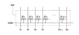
データ駆動部500は、図5に示したように、シフトレジスター部510、ラッチ520、デジタル−アナログ変換器530、バッファー540、そしてチャージシェアリング部550を備える。チャージシェアリング部550は、図6に示したように、隣接したデータ線の間に接続された複数のスイッチング素子SC1、SC2、…、SCm-1を含む。各スイッチング素子SC1、SC2、…、SCm-1は制御端子及び反転制御端子を有しているトランスミッションゲートであり、制御端子にロード信号LOADが印加される。
The
シフトレジスター部510は水平同期開始信号STHの印加を受けると、データクロック信号HCLKによって入力された映像データDATを順にシフトさせて1つの行の映像データDATをラッチ520に伝達する。
シフトレジスター部510は複数のシフトレジスターを含み、各シフトレジスターは決められた量の映像データDATを全部シフトさせた後、シフトクロック信号(図示せず)を次の段のシフトレジスターに送って、1つの画素行の映像データDATがシフトレジスター部510のシフトレジスターに順にシフトされる。
When receiving the application of the horizontal synchronization start signal STH, the
The
ラッチ520はシフトレジスター部510から順に入力を受けた映像データDATをロード信号LOADによってデジタル−アナログ変換機530に出力する。
デジタル−アナログ変換器530は階調電圧生成部800から階調電圧Vgmの入力を受けて反転信号RVSによって共通電圧Vcomに対して正の値を有する階調電圧と負の値を有する階調電圧のうちの各映像データDATに対応するいずれか1つを選択する。そして、デジタル−アナログ変換器530は選択された階調電圧を当該アナログデータ電圧に変換する。
The
The digital-
バッファー540はデジタル−アナログ変換器530からのデータ電圧をチャージシェアリング部550に出力する。
チャージシェアリング部550は、既に説明したように、制御端子にロード信号LOADに印加されるトランスミッションゲートから構成されている。図7に示したように、ロード信号LOADが高レベルを維持する間にトランスミッションゲートSC1-SCm-1は導通状態になって全てのデータ線D1-Dmが互いに接続される。したがって、全てのデータ線D1-Dmの電圧状態は所定の電圧レベルV1に均一となる。つまり、チャージシェアリングが行われる。その後、ロード信号LOADが高レベルから低レベルに変われば、下降エッジ時にトランスミッションゲートSC1-SCm-1の制御端子に低レベルが印加されて、全てのトランスミッションゲートSC1-SCm-1は導通状態から非導通状態に変わり、映像データDATに対応する当該データ電圧がデータ線D1-Dmを通じて伝達される。
The
As described above, the
これによって、ロード信号LOADが高レベルを維持する間にチャージシェアリングが発生してデータ線の電圧DOUTはチャージシェアリングが発生する間に所定電圧V1レベルを維持した後、各当該極性の正規映像データ電圧やインパルシブデータ電圧に変わる。この時、高レベルを維持するロード信号LOADの幅は、十分なチャージシェアリングが行われてデータ線の電圧DOUTが所定レベルの電圧V1に安定的に変り得る程度に広いことが良く、約1μs以上であることが好ましい。また、ロード信号LOADが低レベルから高レベルに変わる時点からゲートクロック信号CPVが低レベルから高レベルに変わる時点までは約1.8μsであることがよい。 As a result, charge sharing occurs while the load signal LOAD is maintained at a high level, and the voltage DOUT of the data line is maintained at a predetermined voltage V1 level while charge sharing is occurring. Changes to data voltage or impulsive data voltage. At this time, the width of the load signal LOAD that maintains the high level should be wide enough that sufficient charge sharing can be performed and the voltage DOUT of the data line can be stably changed to the predetermined voltage V1, about 1 μs. The above is preferable. The time from when the load signal LOAD changes from low level to high level to when the gate clock signal CPV changes from low level to high level is preferably about 1.8 μs.
この時、データ電圧の極性は、ロード信号LOADが低レベルから高レベルに変わって1つの画素行の映像データDATがラッチ520からデジタル−アナログ変換器530に印加される時、反転信号RVSのレベルによって決められる。つまり、反転信号RVSのレベルが高レベルである場合、データ電圧の極性は正(+)の極性を有し、反転信号RVSのレベルが低レベルである場合、データ電圧の極性は負(−)の極性を有するが、これに限定されず反対の場合も可能である。
At this time, when the load signal LOAD changes from low level to high level and the video data DAT of one pixel row is applied from the
このように、データ線D1-Dmに映像データDATに対応するデータ電圧が印加される前に、チャージシェアリング部550を利用して全てのデータ線D1-Dmの電圧レベルを一定の電圧V1レベルに均一化させるチャージシェアリングを実施する。したがって、データ線D1-Dmは、正規映像データ電圧を印加するか、インパルシブデータ電圧を印加しても、全て同一の電圧レベルで当該電圧に変化するので、全ての画素PXは同一の充電条件でインパルシブデータ電圧や正規映像データ電圧への充電動作が行われる。
Thus, before the data voltages corresponding to the image data DAT to the data lines D 1 -D m is applied, a constant voltage level of all the while the data lines D 1 -D m by utilizing the
その結果、ブラック映像データ電圧のようなインパルシブデータ電圧から正規映像データ電圧へ充電される時の充電条件が、正規映像データ電圧から反対極性の正規映像データ電圧へ充電される時の充電条件より有利であるために発生する明るい横線紋の不良が減少する。
この時、データ線に正常データ電圧やブラックデータ電圧が印加される前にデータ駆動部500はロード信号LOADに同期して全てのデータ線を接続するチャージシェアリングを実施する。次に、図5を参照して、このようなデータ駆動部500の動作についてさらに詳細に説明する。
As a result, the charging condition when charging from the impulsive data voltage such as the black video data voltage to the normal video data voltage is more than the charging condition when charging from the normal video data voltage to the normal video data voltage of the opposite polarity. It reduces the bright horizontal line defects that occur due to the advantage.
At this time, before the normal data voltage or the black data voltage is applied to the data line, the
図5は本発明の1つの実施例によるデータ駆動部のブロック図であり、図6は図5に示したチャージシェアリング部の回路図に対する一例である。図7は本発明の1つの実施例によるチャージシェアリング時、ロード信号、ゲートクロック信号、反転信号によって任意の1つのデータ線を流れる電圧に対する波形図である。
データ駆動部500は、図5に示したように、シフトレジスター部510、ラッチ520、デジタル−アナログ変換器530、バッファー540、そしてチャージシェアリング部550を備える。チャージシェアリング部550は、図6に示したように、隣接したデータ線の間に接続された複数のスイッチング素子SC1,SC2,…,SCm-1を含む。各スイッチング素子SC1,SC2,…,SCm-1は制御端子及び反転制御端子を有しているトランスミッションゲートであり、制御端子にロード信号LOADが印加される。
FIG. 5 is a block diagram of a data driver according to an embodiment of the present invention, and FIG. 6 is an example of a circuit diagram of the charge sharing unit shown in FIG. FIG. 7 is a waveform diagram with respect to a voltage flowing through an arbitrary data line by a load signal, a gate clock signal, and an inverted signal during charge sharing according to an embodiment of the present invention.
The
シフトレジスター部510は水平同期開始信号STHの印加を受けると、データクロック信号HCLKによって入力された映像データDATを順にシフトさせ、1つの行の映像データDATをラッチ520に伝達する。シフトレジスター部510は複数のシフトレジスターを含み、シフトレジスターが担当する映像データDATを全部シフトさせた後、シフトクロック信号(図示せず)を次の段のシフトレジスターに伝送して映像データDATのシフト動作を行う。よって、1つの画素行の映像データDATがシフトレジスター部510のシフトレジスターに順にシフトされる。
When receiving the application of the horizontal synchronization start signal STH, the
ラッチ520はシフトレジスター部510から順に入力を受けた映像データDATをロード信号LOADによってデジタル−アナログ変換器530に出力する。
デジタル−アナログ変換器530は階調電圧生成部800から階調電圧Vgmの入力を受けて反転信号RVSによって共通電圧Vcomに対して正の値を有する階調電圧と負の値を有する階調電圧のうちのいずれか1つを選択する。そして、選択された階調電圧の中で各映像データDATに対応する階調電圧を選択し、デジタル映像データDATを当該アナログデータ電圧に変換する。
The
The digital-
バッファー540はデジタル−アナログ変換器530からのデータ電圧をチャージシェアリング部550に出力する。
チャージシェアリング部550は、既に説明したように、制御端子にロード信号LOADに印加されるトランスミッションゲートから構成されている。図7に示したように、ロード信号LOADが高レベルを維持する間に、トランスミッションゲートSC1-SCm-1は導通状態になって、全てのデータ線D1-Dmが互いに接続される。したがって、全てのデータ線D1-Dmの電圧状態は所定の電圧レベルV1に均一となる。つまり、チャージシェアリングが行われる。その後、ロード信号LOADが高レベルから低レベルに変われば、つまり、下降エッジ時にトランスミッションゲートSC1-SCm-1の制御端子に低レベルが印加されて、全てのトランスミッションゲートSC1-SCm-1は導通状態から非導通状態に変わり、映像データDATに対応する当該データ電圧がデータ線D1-Dmを通じて伝達される。
The
As described above, the
その結果、ロード信号LOADが高レベルを維持する間にチャージシェアリングが発生し、データ線の電圧DOUTはチャージシェアリングが発生する間に所定電圧V1レベルを維持した後、各当該極性の正常データ電圧やインパルシブデータ電圧に変わる。この時、高レベルを維持するロード信号LOADの幅は充分なチャージシェアリングが行われてデータ線の電圧DOUTが所定レベルの電圧V1に安定的に変わり得る程度に広いことがよく、約1μs以上であるのが好ましい。また、ロード信号LOADが低レベルから高レベルに変わる時点からゲートクロック信号CPVが低レベルから高レベルに変わる時点までは約1.8μsであるのがよい。 As a result, charge sharing occurs while the load signal LOAD remains high, and the voltage DOUT of the data line maintains the predetermined voltage V1 level while charge sharing occurs, and then normal data of each relevant polarity. Change to voltage or impulsive data voltage. At this time, the width of the load signal LOAD for maintaining the high level should be wide enough that sufficient charge sharing is performed and the voltage DOUT of the data line can be stably changed to the predetermined voltage V1. Is preferred. The time from when the load signal LOAD changes from low level to high level to when the gate clock signal CPV changes from low level to high level is preferably about 1.8 μs.
この時、データ電圧の極性はロード信号LOADが低レベルから高レベルに変わって、1つの画素行の映像データDATがラッチ520からデジタル−アナログ変換器530に印加される時、反転信号RVSのレベルによって決められる。つまり、反転信号RVSのレベルが高レベルである場合にデータ電圧の極性は正(+)の極性を有し、反転信号RVSのレベルが低レベルである場合にデータ電圧の極性は負(−)の極性を有するが、これに限定されず、反対の場合も可能である。
At this time, the polarity of the data voltage is such that the load signal LOAD changes from low level to high level, and when the video data DAT of one pixel row is applied from the
このように、データ線D1-Dmに映像データDATに対応するデータ電圧が印加される前にチャージシェアリング部550を利用して全てのデータ線D1-Dmの電圧レベルを一定の電圧V1レベルに均一化するチャージシェアリングを実施する。したがって、データ線D1-Dmにより正常データ電圧を印加する場合、インパルシブデータ電圧を印加する場合のいずれの場合も全て同一の電圧レベルから当該電圧に変化するので、全ての画素は同一の充電条件でインパルシブデータ電圧や映像データ電圧への充電動作が行われる。
Thus, while the data lines D 1 -D m all while the data lines D 1 -D m of the voltage level constant by utilizing the
これによって、ブラック映像データから正常データ電圧へ充電される時の充電条件が、正常データ電圧から反対極性の正常データ電圧へ充電される時の充電条件より有利であるために発生する明るい横線紋の不良が減る。つまり、インパルシブ駆動のためにインパルシブデータ電圧が印加された後、正常データ電圧が印加される場合や、極性が反対である正常データ電圧に変わる場合、全て同一な電圧レベルV1から当該データ電圧に変わるので、同一な充電条件で画素の充電動作が行われる。 As a result, the bright horizontal line pattern generated because the charging condition when charging from the black video data to the normal data voltage is more advantageous than the charging condition when charging from the normal data voltage to the normal data voltage of the opposite polarity. Defects are reduced. In other words, when the normal data voltage is applied after the impulsive data voltage is applied for the impulsive driving, or when the normal data voltage is changed to the opposite polarity, the data voltage is changed from the same voltage level V1 to the data voltage. Therefore, the pixel charging operation is performed under the same charging condition.
本発明の他の実施例による液晶表示装置について図8を図1と共に参照して詳細に説明する。但し、上述した実施例と同一の部分についての詳細な説明は省略する。
図8は本発明の他の実施例による液晶表示装置の2つの副画素に対する等価回路図である。
図1に示すように、本発明の他の実施例による液晶表示装置も液晶表示板組立体300、ゲート駆動部400、データ駆動部500、階調電圧生成部800、そして信号制御部600を含む。
A liquid crystal display device according to another embodiment of the present invention will be described in detail with reference to FIG. 8 together with FIG. However, detailed description of the same parts as those in the above-described embodiment will be omitted.
FIG. 8 is an equivalent circuit diagram for two sub-pixels of a liquid crystal display device according to another embodiment of the present invention.
As shown in FIG. 1, a liquid crystal display according to another embodiment of the present invention also includes a liquid
液晶表示板組立体300は、図8に示したように、等価回路で見る時、複数の信号線(図示せず)と、これに接続されていてほぼ行列形態で配列された複数の画素PXを含む。液晶表示板組立体300は互いに対向する下部及び上部表示板100、200と、その間に入っている液晶層3を含む。
信号線はゲート信号(“走査信号”とも言う)を伝達する複数のゲート線(図示せず)とデータ信号を伝達する複数のデータ線(図示せず)を含む。ゲート線はほぼ行方向に延びた互いにほぼ平行であり、データ線はほぼ列方向に延びて互いにほぼ平行である。
As shown in FIG. 8, the liquid
The signal lines include a plurality of gate lines (not shown) that transmit gate signals (also referred to as “scanning signals”) and a plurality of data lines (not shown) that transmit data signals. The gate lines are substantially parallel to each other extending in the row direction, and the data lines are substantially parallel to each other extending in the column direction.
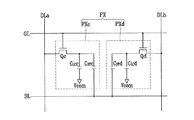
各画素PXは一対の副画素を含み、各副画素は液晶キャパシタCLCa、CLCbを含む。2つの副画素のうちの少なくとも1つはゲート線、データ線及び液晶キャパシタCLCa、CLCbと接続されたスイッチング素子(図示せず)を含む。
液晶キャパシタCLCa/CLCbは下部表示板100の副画素電極PEa/PEbと上部表示板200の共通電極CEを2つの端子とし、副画素電極PEa/PEbと共通電極CEの間の液晶層3は誘電体として機能する。一対の副画素電極PEa、PEbは互いに分離されており、1つの画素電極PEを構成する。共通電極CEは上部表示板200の前面に形成されていて共通電圧Vcomの印加を受ける。液晶層3は負の誘電率異方性を有し、液晶層3の液晶分子は電場がない状態でその長軸が2つの表示板の表面に対して垂直または水平をなすように配向されていてもよい。
Each pixel PX includes a pair of sub-pixels, and each sub-pixel includes liquid crystal capacitors C LC a and C LC b. At least one of the two sub-pixels includes a switching element (not shown) connected to the gate line, the data line, and the liquid crystal capacitors C LC a and C LC b.
The liquid crystal capacitors C LC a / C LC b have the sub-pixel electrodes PEa / PEb of the
一方、色表示を実現するためには、各画素PXが空間分割または時間分割方式で表示することができる。図8は空間分割の一例で、各画素PXが上部表示板200の領域に基本色のうちの1つを示す色フィルターCFを備えることを示している。図8とは異なって、色フィルターCFは下部表示板100の第1及び第2副画素電極PEa、PEbの上または下に形成してもよい。
On the other hand, in order to realize color display, each pixel PX can be displayed by space division or time division. FIG. 8 shows an example of space division, and each pixel PX includes a color filter CF indicating one of the basic colors in the area of the
表示板100、200の外側面には偏光子(図示せず)が設けられているが、2つの偏光子の偏光軸を直交状態に構成することができる。反射型液晶表示装置の場合には、2つの偏光子のうちの1つを省略できる。直交偏光子である場合、電場のない液晶層3に入った入射光を遮断する。
階調電圧生成部800は画素PXの透過率と関する少なくとも2つの階調電圧集合(または基準階調電圧集合)を生成する。少なくとも2つの(基準)階調電圧集合は互いに異なるガンマ曲線に基づいて生成され、各(基準)階調電圧集合は共通電圧Vcomに対して正の値を有するものと負の値を有するものを含む。しかし、少なくとも2つの(基準)階調電圧集合の代わりに1つの(基準)階調電圧集合のみを生成することもできる。
Although polarizers (not shown) are provided on the outer surfaces of the
The
以下では、このような液晶表示装置の動作について詳細に説明する。
信号制御部600は外部のグラフィック制御機から入力映像信号R、G、B及びその表示を制御する入力制御信号を受信する。
信号制御部600は入力映像信号R、G、Bと入力制御信号に基づいて入力映像信号R、G、Bを液晶表示板組立体300及びデータ駆動部500の動作条件に合わせて適切に処理し、ゲート制御信号CONT1及びデータ制御信号CONT2などを生成した後、ゲート制御信号CONT1をゲート駆動部400に出力して、データ制御信号CONT2と処理した映像信号DATをデータ駆動部500に出力する。出力映像信号DATは入力映像信号R、G、Bに基づいて作った正規映像データとインパルシブ駆動のためのインパルシブデータを含む。
Hereinafter, the operation of such a liquid crystal display device will be described in detail.
The
The
ゲート制御信号CONT1は走査開始信号STV、ゲートクロック信号CPV及び少なくとも1つの出力イネーブル信号OEを含む。
データ制御信号CONT2は1つの束の副画素に対する映像データの伝送開始を知らせる水平同期開始信号STHと、液晶表示板組立体300にデータ信号を印加することを命令するロード信号LOAD、データクロック信号HCLK及び反転信号RVSを含む。
The gate control signal CONT1 includes a scan start signal STV, a gate clock signal CPV, and at least one output enable signal OE.
The data control signal CONT2 includes a horizontal synchronization start signal STH for informing the start of transmission of video data to one bundle of sub-pixels, a load signal LOAD for instructing application of the data signal to the liquid
信号制御部600からのデータ制御信号CONT2によってデータ駆動部500は1つの束の副画素に対する出力映像信号DATを受信し、各出力映像信号DATに対応する階調電圧を選択することによってデジタル映像信号DATをアナログデータ電圧Vdに変換した後、これを当該データ線に印加する。
ゲート駆動部400は信号制御部600からのゲート制御信号CONT1によってゲートオン電圧Vonをゲート線に印加して、このゲート線に接続されたスイッチング素子を導通させる。その結果、データ線に印加されたデータ信号が導通したスイッチング素子を通じて当該副画素PXa、PXbに印加される。
In response to the data control signal CONT2 from the
The
1つの画素電極PEをなす一対の副画素電極PEa、PEbが別個のスイッチング素子と接続されている場合、つまり、各副画素が各々のスイッチング素子を有している場合には、2つの副画素が互いに異なる時間に同一のデータ線を通じて別個のデータ電圧の印加を受けることができ、また、同一の時間に互いに異なるデータ線を通じて別個のデータ電圧の印加を受けることもできる。これとは異なって、副画素電極PEaはスイッチング素子(図示せず)と接続されていて、副画素電極PEbは副画素電極PEaと容量性結合されている場合には、副画素電極PEaを含む副画素のみスイッチング素子を通じてデータ電圧の印加を受け、副画素電極PEbを含む副画素は副画素電極PEaの電圧変化によって変化する電圧を有することができる。この時、副画素電極PEaの面積は副画素電極PEbの面積より小さく、副画素電極PEaの電圧は副画素電極PEbの電圧より大きい。 When a pair of sub-pixel electrodes PEa and PEb forming one pixel electrode PE are connected to separate switching elements, that is, when each sub-pixel has a respective switching element, two sub-pixels May receive different data voltages through the same data line at different times, and may receive different data voltages through different data lines at the same time. In contrast, when the subpixel electrode PEa is connected to a switching element (not shown) and the subpixel electrode PEb is capacitively coupled to the subpixel electrode PEa, the subpixel electrode PEa includes the subpixel electrode PEa. Only the sub-pixel receives a data voltage through the switching element, and the sub-pixel including the sub-pixel electrode PEb may have a voltage that changes according to the voltage change of the sub-pixel electrode PEa. At this time, the area of the subpixel electrode PEa is smaller than the area of the subpixel electrode PEb, and the voltage of the subpixel electrode PEa is larger than the voltage of the subpixel electrode PEb.
このように液晶キャパシタCLCa、CLCbの両端に電位差が生じれば、表示板100、200の表面にほとんど垂直の電場(電界)が液晶層3に生成される(以下、画素電極PE及び共通電極CEを同様に“電場生成電極”と言う)。その結果、液晶層3の液晶分子は電場に応答してその長軸が電場の方向に垂直をなすように傾き、液晶分子が傾いた程度によって液晶層3に入射光の偏光の変化程度が変わる。このような偏光の変化は偏光子によって透過率の変化で現れ、これによって液晶表示装置は映像を表示する。
Thus, if a potential difference occurs between both ends of the liquid crystal capacitors C LCa and C LC b, an electric field (electric field) almost perpendicular to the surfaces of the
液晶分子が傾く角度は電場の強さによって変わるが、2つの液晶キャパシタCLCa、CLCbの電圧が互いに異なるので、液晶分子が傾いた角度が異なり、そのために2つの副画素の輝度が異なる。したがって、液晶キャパシタCLCaの電圧と液晶キャパシタCLCbの電圧を適切に合わせば、側面から見る映像を正面から見る映像に最大限に近くすることができ、つまり、側面ガンマ曲線を正面ガンマ曲線に最大限に近くすることができ、このようにして側面視認性を向上させることができる。 The angle at which the liquid crystal molecules are tilted varies depending on the strength of the electric field, but since the voltages of the two liquid crystal capacitors C LC a and C LC b are different from each other, the angles at which the liquid crystal molecules are tilted are different. Different. Therefore, if the voltage of the liquid crystal capacitor C LC a and the voltage of the liquid crystal capacitor C LC b are appropriately matched, the image seen from the side can be maximized to the image seen from the front. The curve can be as close as possible to the maximum, and thus the side visibility can be improved.
また、高い電圧の印加を受ける副画素電極PEaの面積を副画素電極PEbの面積より小さくすれば、側面ガンマ曲線を正面ガンマ曲線にさらに近くすることができる。特に、副画素電極PEa、PEbの面積比をほぼ1:2とすれば、側面ガンマ曲線が正面ガンマ曲線により近くなって側面視認性がさらに良くなる。
1水平周期(“1H”とも言う)を単位としてこのような過程を繰り返すことによって、全ての副画素PXa、PXbにデータ電圧Vdを印加して1つのフレームの正規映像及びインパルシブ映像を表示する。
Further, if the area of the subpixel electrode PEa that receives a high voltage is made smaller than the area of the subpixel electrode PEb, the side gamma curve can be made closer to the front gamma curve. In particular, when the area ratio of the sub-pixel electrodes PEa and PEb is approximately 1: 2, the side gamma curve becomes closer to the front gamma curve and the side visibility is further improved.
By repeating such a process in units of one horizontal period (also referred to as “1H”), the data voltage Vd is applied to all the subpixels PXa and PXb to display a normal image and an impulsive image of one frame.
1つのフレームが終われば、次のフレームが始まり、各副画素PXa、PXbに印加されるデータ電圧Vdの極性が直前フレームにおける極性と反対になるようにデータ駆動部500に印加される反転信号RVSの状態を制御することができる。また、1つのフレーム内でも行反転、点反転、列反転などの極性反転方式によってデータ駆動部500に印加される反転信号RVSの状態を制御することができる。
When one frame ends, the next frame starts, and the inverted signal RVS applied to the
一方、1つのフレームの間に副画素PXaには正規映像データに基づいた正規映像を表示し、副画素PXbには正規映像データに基づいた正規映像及びインパルシブデータに基づいたインパルシブ映像を1回ずつ表示する。このように副画素PXbにのみインパルシブ映像を表示しても、副画素電極PEaに対する副画素電極PEbの面積比を大きくして全体画面に対するインパルシブ映像の表示比率を高めれば、副画素PXa、PXbにインパルシブ映像を表示することと同様の水準でブラリングを減少することができる。 On the other hand, a normal image based on normal video data is displayed on the sub-pixel PXa during one frame, and a normal video based on normal video data and an impulsive video based on impulsive data are displayed once on the sub-pixel PXb. Display one by one. Thus, even if an impulsive image is displayed only on the subpixel PXb, if the area ratio of the subpixel electrode PEb to the subpixel electrode PEa is increased to increase the display ratio of the impulsive image to the entire screen, the subpixels PXa and PXb are displayed. The blurring can be reduced at the same level as displaying impulsive video.
次に、図8に示した2つの副画素が互いに異なる時間に同一のデータ線を通じて別個のデータ電圧の印加を受ける本発明の他の実施例による液晶表示装置について図9を参照して詳細に説明する。
図9は本発明の他の実施例による液晶表示装置の1つの画素に対する等価回路図である。
Next, a liquid crystal display device according to another embodiment of the present invention in which the two sub-pixels shown in FIG. 8 receive different data voltages through the same data line at different times will be described in detail with reference to FIG. explain.
FIG. 9 is an equivalent circuit diagram for one pixel of a liquid crystal display device according to another embodiment of the present invention.
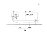
図9に示すように、本実施例による液晶表示装置は複数対のゲート線GLa、GLb、複数のデータ線DL及び複数の維持電極線SLを含む信号線と、これに接続された複数の画素PXを含む。
各画素PXは一対の副画素PXa、PXbを含み、各副画素PXa/PXbは各々当該ゲート線GLa/GLb及びデータ線DLに接続されているスイッチング素子Qa/Qbと、これに接続された液晶キャパシタCLCa/CLCb、そしてスイッチング素子Qa/Qb及び維持電極線SLに接続されているストレージキャパシタCSTa/CSTbを含む。
As shown in FIG. 9, the liquid crystal display device according to the present embodiment includes signal lines including a plurality of pairs of gate lines GLa and GLb, a plurality of data lines DL, and a plurality of storage electrode lines SL, and a plurality of pixels connected thereto. Includes PX.
Each pixel PX includes a pair of sub-pixels PXa and PXb, and each sub-pixel PXa / PXb includes a switching element Qa / Qb connected to the gate line GLa / GLb and the data line DL, and a liquid crystal connected thereto. The capacitor C LC a / C LC b and the storage capacitor C ST a / C ST b connected to the switching element Qa / Qb and the storage electrode line SL are included.
各スイッチング素子Qa/Qbは下部表示板100に設けられている薄膜トランジスタなどの三端子素子であって、その制御端子はゲート線GLa/GLbに接続されており、入力端子はデータ線DLに接続されており、出力端子は液晶キャパシタCLCa/CLCb及びストレージキャパシタCSTa/CSTbに接続されている。
液晶キャパシタCLCa/CLCbの補助的な役割を果たすストレージキャパシタCSTa/CSTbは、下部表示板100に設けられた維持電極線SLと画素電極PEが絶縁体を間に挟んで重合して構成され、維持電極線SLには共通電圧Vcomなどの所定の電圧が印加される。しかし、ストレージキャパシタCSTa、CSTbは副画素電極PEa、PEbが絶縁体を媒介として直上の前段ゲート線と重合するように構成してもよい。
Each switching element Qa / Qb is a three-terminal element such as a thin film transistor provided on the
The liquid crystal capacitor C LC a / C LC b auxiliary role storage capacitor C ST a / C ST b is the storage electrode line provided on the
液晶キャパシタCLCa、CLCbなどについては上述したので、詳細な説明を省略する。
次に、このような液晶表示装置の動作について図10及び図11を参照して詳細に説明する。
図10は図9に示した画素を含む液晶表示装置の駆動信号を示したタイミング図であり、図11は図10に示した駆動信号によって表示される画像を1つのフレームの間に表示した概略図である。
Since the liquid crystal capacitors C LCa and C LC b have been described above, a detailed description thereof will be omitted.
Next, the operation of such a liquid crystal display device will be described in detail with reference to FIGS.
FIG. 10 is a timing chart showing a driving signal of the liquid crystal display device including the pixel shown in FIG. 9, and FIG. 11 is a schematic diagram showing an image displayed by the driving signal shown in FIG. 10 during one frame. FIG.
図9に示した画素を含む液晶表示装置では、信号制御部600が入力映像信号R、G、Bを受信して副画素PXaに対する正規映像データNaと副画素PXbに対する正規映像データNb及びインパルシブデータIを含む出力映像信号DATに変換してデータ駆動部500に伝送する。
信号制御部600はM個の束の入力映像信号R、G、Bを受けて各M個の束の正規映像データNa、Nbに変換し、1つの束のインパルシブデータIを生成してM個の束の入力映像信号R、G、Bが入力される時間と実質的に同一な時間の間に(2M+1)個の束の出力映像信号DATを出力する(Mは自然数)。したがって、水平同期開始信号STHの周波数は水平同期信号Hsyncの周波数の(2M+1)/M倍である。また、出力映像信号DATが同期されるデータクロック信号HCLKの周波数は入力映像信号R、G、Bが同期されるメインクロックMCLKの周波数の(2M+1)/M倍であり得る。例えば、図10にはMを3として示した。
In the liquid crystal display device including the pixels shown in FIG. 9, the
The
データ駆動部500は1つの副画素行の出力映像信号DATを受信し、各出力映像信号DATに対応する階調電圧を選択することによって出力映像信号DATをアナログデータ電圧Vdに変換した後、これを当該データ線DLに印加する。
階調電圧生成部800で1つの階調電圧集合を作って、正規映像データNa、Nbを互いに異ならせて各画素PXa、PXbに互いに異なる電圧を印加することができる。しかし、正規映像データNa、Nbは同一でありながら2つの副画素PXa、PXbに対する階調電圧集合を別に作り、これを交互にデータ駆動部500に提供することができ、また、データ駆動部500でこれを交互に選択することによって、2つの副画素PXa、PXbに互いに異なる電圧を印加することもできる。但し、この時、2つの副画素PXa、PXbの合成ガンマ曲線が正面での基準ガンマ曲線に近く映像信号を補正したり、階調電圧集合を作ることが好ましい。例えば、正面での合成ガンマ曲線は、この液晶表示板組立体に最も適するように決められた正面での基準ガンマ曲線と一致するようにし、側面での合成ガンマ曲線は正面での基準ガンマ曲線と最も近くする。
The
The
インパルシブデータIに対しても階調電圧生成部800は別途の階調電圧集合を生成することができ、正規映像データNa、Nb用階調電圧集合を使用することもできる。
図10に示したように、データ駆動部500は第1〜第6水平周期の間に第1〜第3番目画素行の各副画素PXa、PXbに対するデータ電圧Vdを1Hごとに順に当該データ線DLに印加する。
Also for the impulsive data I, the
As shown in FIG. 10, the
ゲート駆動部400もこれに同期して第1〜第6水平周期の間に第1〜第3番目画素行の副画素PXa、PXbに各々接続されているゲート線GLa、GLbにゲート信号g1a-g3bを1Hごとに順に印加して、これらゲート線GLa、GLbに各々接続されているスイッチング素子Qa、Qbを導通させる。その結果、データ線DLに印加された正規映像データNa、Nbに相当するデータ電圧Vdが導通したスイッチング素子Qa、Qbを通じて当該副画素PXa、PXbに各々印加される。
In synchronism with this, the
そして、データ駆動部500は第7水平周期TIの間にインパルシブデータIに対するデータ電圧Vdをデータ線DLに印加する。
第7水平周期TIでゲート駆動部400はゲート信号gkb、gk+1b、gk+2bを各々k〜(k+2)番目画素行の副画素PXbに接続されたゲート線GLbに同時に印加して、このゲート線GLbに接続されたスイッチング素子Qbを導通させる。その結果、データ線DLに印加されたインパルシブデータIに対応するデータ電圧Vdが導通したたスイッチング素子Qbを通じて当該画素PXbに印加される。
The
In the seventh horizontal period TI, the
このような方式で3画素行ごとに6水平周期の間に正規映像データNa、Nbに対応するデータ電圧Vdを当該副画素PXa、PXbに印加し、1水平周期の間にインパルシブデータIに対応するデータ電圧Vdを当該副画素PXbに印加する。1つのフレームの間に全ての副画素PXaに正規映像データNaに対応するデータ電圧Vdを印加し、全ての副画素PXbに正規映像データNb及びインパルシブデータIに対応するデータ電圧Vdを1回ずつ印加して、一つのフレームの正規映像及びインパルシブ映像を表示する。 In this manner, the data voltage Vd corresponding to the normal video data Na and Nb is applied to the sub-pixels PXa and PXb during 6 horizontal periods every 3 pixel rows, and the impulsive data I is applied during one horizontal period. A corresponding data voltage Vd is applied to the subpixel PXb. Data voltage Vd corresponding to normal video data Na is applied to all subpixels PXa during one frame, and data voltage Vd corresponding to normal video data Nb and impulsive data I is applied to all subpixels PXb once. The normal image and the impulsive image of one frame are displayed by applying them one by one.
図11に正規映像及びインパルシブ映像が1つのフレームの間に表示される過程が示されている。図4と同様に、kはn/4とし(nは縦解像度)、表示されるパターンは図4と実質的に同一なので、これについての詳細な説明は省略する。ただし、斜線の部分のようにインパルシブ映像が表示されている領域の副画素PXaには正規映像が表示されているので、この領域での輝度が図4に示されている同一な領域における輝度に比べて高い。 FIG. 11 shows a process in which the regular video and the impulsive video are displayed during one frame. As in FIG. 4, k is n / 4 (n is vertical resolution), and the displayed pattern is substantially the same as in FIG. 4, so detailed description thereof will be omitted. However, since the normal image is displayed on the sub-pixel PXa in the area where the impulsive image is displayed, such as the shaded portion, the luminance in this area is equal to the luminance in the same area shown in FIG. Higher than that.
本実施例ではインパルシブ映像を副画素PXbに表示することと説明したが、これと反対に、インパルシブ映像を副画素PXaに表示することもできる。
このようにインパルシブ映像を2つの副画素PXa、PXbのうちのいずれか1つに表示し、他の副画素には正規映像を表示することによって、ブラリングを防止しながら輝度低下を減らすことができる。また、複数行の副画素にインパルシブ映像を同時に表示することで、インパルシブ駆動のための周波数の増加が相対的に少ないので画素電圧の充電率を高めることができる。
In the present embodiment, it has been described that the impulsive video is displayed on the sub-pixel PXb. On the contrary, the impulsive video can be displayed on the sub-pixel PXa.
In this way, the impulsive video is displayed on one of the two sub-pixels PXa and PXb, and the normal video is displayed on the other sub-pixels, thereby reducing brightness reduction while preventing blurring. it can. In addition, by simultaneously displaying impulsive images on a plurality of rows of sub-pixels, the increase in frequency for impulsive driving is relatively small, so that the charging rate of the pixel voltage can be increased.
図2〜図4に示した液晶表示装置の多くの特徴が図8〜図11に示した液晶表示装置にも適用できる。
以下では図9に示した画素を有する液晶表示装置におけるインパルシブ映像を表示するための他の駆動方法について図12を参照して詳細に説明する。
図12は本発明の他の実施例による液晶表示装置の駆動信号の他の例を示したタイミング図である。
Many features of the liquid crystal display device shown in FIGS. 2 to 4 can be applied to the liquid crystal display device shown in FIGS.
Hereinafter, another driving method for displaying an impulsive image in the liquid crystal display device having the pixels shown in FIG. 9 will be described in detail with reference to FIG.
FIG. 12 is a timing diagram showing another example of a driving signal of a liquid crystal display device according to another embodiment of the present invention.
図12に示したタイミング度は3画素行単位でデータ電圧の極性が変わる行反転である場合の駆動信号に関する。
図12に示したように、データ駆動部500は第1〜第6水平周期の間に第1〜第3番目画素行の各副画素PXa、PXbに対する正極性のデータ電圧を1Hごとに順に当該データ線DLに印加する。
The timing shown in FIG. 12 relates to a drive signal in the case of row inversion in which the polarity of the data voltage changes in units of 3 pixel rows.
As shown in FIG. 12, the
ゲート駆動部400もこれに同期して第1〜第6水平周期の間に第1〜第3番目画素行の副画素PXa、PXbに各々接続されているゲート線GLa、GLbにゲート信号g1a-g3bを1Hごとに順に印加して、これらゲート線GLa、GLbに各々接続されているスイッチング素子Qa、Qbを導通させる。その結果、データ線DLに印加された正規映像データNa、Nbに相当する正極性のデータ電圧Vdが導通したスイッチング素子Qa、Qbを通じて当該副画素PXa、PXbに各々印加される。
In synchronism with this, the
そして、データ駆動部500は第7水平周期の間にインパルシブデータIに対するデータ電圧Vdをデータ線DLに印加する。
第7水平周期でゲート駆動部400はゲート信号gkb、gk+1b、gk+2bを各々k〜(k+2)番目画素行の副画素PXbに接続されたゲート線GLbに同時に印加して、このゲート線GLbに接続されたスイッチング素子Qbを導通させる。その結果、データ線DLに印加されたインパルシブデータIに対応するデータ電圧Vdが導通したスイッチング素子Qbを通じて当該画素PXbに印加される。
The
In the seventh horizontal period, the
その後、データ駆動部500は所定時間TCの間に所定の負極性データ電圧を印加する。しかし、いずれのゲート線にもゲートオン電圧Vonを印加しない。ここで、所定時間TCは1水平周期と同一であってもよく、これと異なってもよい。また、所定の負極性データ電圧は第4画素行の副画素PXaに印加される正規映像データNaに対する負極性データ電圧に基づいて決められてもよく、一定の値を有してもよい。
Thereafter, the
このような方式で3画素行ごとに6水平周期の間に正規映像データNa、Nbに対応するデータ電圧Vdを当該副画素PXa、PXbに印加し、1水平周期の間にインパルシブデータIに対応するデータ電圧Vdを当該副画素PXbに印加し、所定時間TCの間に直前データ電圧Vdの極性と異なる極性のデータ電圧を印加して先充電する。1つのフレームの間に全ての副画素PXaに正規映像データNaに対応するデータ電圧Vdを印加し、全ての副画素PXbに正規映像データNb及びインパルシブデータIに対応するデータ電圧Vdを1回ずつ印加して、1つのフレームの正規映像及びインパルシブ映像を表示する。 In this manner, the data voltage Vd corresponding to the normal video data Na and Nb is applied to the sub-pixels PXa and PXb during 6 horizontal periods every 3 pixel rows, and the impulsive data I is applied during one horizontal period. A corresponding data voltage Vd is applied to the sub-pixel PXb, and a data voltage having a polarity different from the polarity of the immediately preceding data voltage Vd is applied for a predetermined time TC for precharging. Data voltage Vd corresponding to normal video data Na is applied to all subpixels PXa during one frame, and data voltage Vd corresponding to normal video data Nb and impulsive data I is applied to all subpixels PXb once. The normal image and the impulsive image of one frame are displayed by applying them one by one.
その結果、図12に示したように、副画素PXa、PXbには正極性と負極性の画素電圧Vpが3画素行ごとに交互に充電され、極性が変わる時、所定時間TCの間に次に変わる極性を有する所定のデータ電圧でデータ線DLを先充電するので、画素電圧Vpの充電率が高まる。
図10及び図11に示した液晶表示装置の多くの特徴が図12に示した液晶表示装置にも適用できる。
As a result, as shown in FIG. 12, the subpixels PXa and PXb are alternately charged with the positive and negative pixel voltages Vp every three pixel rows, and when the polarity changes, Since the data line DL is precharged with a predetermined data voltage having a polarity that changes to, the charging rate of the pixel voltage Vp is increased.
Many features of the liquid crystal display device shown in FIGS. 10 and 11 can be applied to the liquid crystal display device shown in FIG.
次に、図9に示した画素を有する液晶表示装置でインパルシブ映像を表示するための他の駆動方法について図13を参照して詳細に説明する。
図13は本発明の他の実施例による液晶表示装置の駆動信号の他の例を示したタイミング図である。
信号制御部600は入力映像信号R、G、Bを副画素PXa、PXbに対する正規映像データに変換するが、インパルシブデータは別途に作らない。
Next, another driving method for displaying an impulsive image on the liquid crystal display device having the pixels shown in FIG. 9 will be described in detail with reference to FIG.
FIG. 13 is a timing diagram showing another example of a driving signal of a liquid crystal display device according to another embodiment of the present invention.
The
階調電圧生成部800は2つの副画素PXa、PXbに対する階調電圧集合を別に作り、これを交互にデータ駆動部500に提供したり、データ駆動部500でこれを交互に選択する。
データ駆動部500は、図5〜図7を参照して既に説明したように、一定の時間の間にデータ駆動部500の全ての出力端子を内部で互いに接続するチャージシェアリング機能を有している。データ駆動部500からのデータ電圧のうちのその半分が正極性で、残り半分は負極性であれば、全体データ線DLのうちの半分は正極性のデータ電圧が充電され、残り半分は負極性のデータ電圧が充電される。したがって、データ駆動部500が全ての出力端子を接続すれば、データ線DLの電荷が互いに再配列されながら、データ駆動部500の出力端子には正極性と負極性の中間値であるほぼ共通電圧Vcomのレベルを有する電荷共有電圧Iがかかる。
The
As already described with reference to FIGS. 5 to 7, the
電荷を共有する状態でゲート駆動部400がゲートオン電圧Vonを所定画素行の副画素PXbに印加して、電荷共有電圧Iが所定画素行の副画素PXbに印加されるようにする。電荷共有電圧Iはインパルシブデータ電圧として使用される。
図13に示すように、1H区間はロード信号LOADがローレベルであるデータ電圧出力区間とハイレバルであるチャージシェアリング区間に分けられる。
The
As shown in FIG. 13, the 1H section is divided into a data voltage output section in which the load signal LOAD is at a low level and a charge sharing section in which the load signal LOAD is at a high level.
データ駆動部500は信号制御部600から1つの画素行の正規映像データを受信し、データ電圧出力区間のうちの前半部で階調電圧生成部800からの副画素PXaに対する階調電圧集合から正規映像データに対応する階調電圧を選択してデータ電圧Naとしてデータ線DLに印加する。
ゲート駆動部400は副画素PXaに接続されているゲート線GLaにゲートオン電圧Vonを印加して、データ線DLに印加されたデータ電圧Naを当該副画素PXaに印加する。
The
The
そして、データ電圧出力区間の後半部で階調電圧生成部800が副画素PXbに対する階調電圧集合をデータ駆動部500に提供するように構成でき、データ駆動部500がこれを選択することによって副画素PXbに対するデータ電圧Nbをデータ線DLに印加するように構成する。
再び、ゲート駆動部400は副画素PXbに接続されているゲート線GLbにゲートオン電圧Vonを印加してデータ線DLに印加されたデータ電圧Nbを当該副画素PXbに印加する。
In the second half of the data voltage output period, the
Again, the
その後、ロード信号LOADがハイレバルになれば、チャージシェアリング区間が始まり、データ駆動部500は全体データ線DLの電荷を共有し、その結果、電荷共有電圧Iがデータ線DLにかかる。
これと同時に、ゲート駆動部400は所定の画素行(例えば、k番目画素行)の副画素PXbに接続されているゲート線GLbにゲートオン電圧Vonを印加して当該副画素PXbに電荷共有電圧Iを印加させる。
Thereafter, when the load signal LOAD becomes high level, the charge sharing period starts, and the
At the same time, the
1水平周期を単位としてこのような過程を繰り返すことによって、全ての副画素PXa、PXbに正規映像及び電荷共有電圧Iによるインパルシブ映像を1つのフレームの間に表示する。
図13に示したように、複数の水平周期の間に1つの画素行の副画素PXbに電荷共有電圧Iを印加したり、複数の画素行の副画素PXbに電荷共有電圧Iを同時に印加したりすることができる。その結果、電荷共有区間が短くても電荷共有電圧Iを副画素PXbに十分に充電することができる。
By repeating such a process in units of one horizontal period, a normal image and an impulsive image based on the charge sharing voltage I are displayed in one frame on all the subpixels PXa and PXb.
As shown in FIG. 13, the charge sharing voltage I is applied to the sub-pixel PXb of one pixel row during a plurality of horizontal periods, or the charge sharing voltage I is simultaneously applied to the sub-pixel PXb of the plurality of pixel rows. Can be. As a result, the charge sharing voltage I can be sufficiently charged to the subpixel PXb even if the charge sharing section is short.
データ電圧出力区間で副画素PXa、PXbにデータ電圧Na、Nbを各々印加する区間の長さは互いに同一でなくてもよい。
このように本実施例によれば、別途のインパルシブデータを生成せずデータ駆動部500の出力端子で電荷共有を通じてインパルシブ映像のための電圧を供給するので、信号制御部600及びデータ駆動部500の動作が簡単で、階調電圧生成部800が別途の階調電圧集合を作る必要がない。また、データ電圧の極性が行反転または点反転である場合、データ線DLが共通電圧Vonレベルに十分に充電されているので、画素電圧の充電率も高めることができる。
The lengths of the sections in which the data voltages Na and Nb are respectively applied to the subpixels PXa and PXb in the data voltage output section may not be the same.
As described above, according to the present embodiment, voltage for impulsive video is supplied through charge sharing at the output terminal of the
図10及び図11に示した液晶表示装置の多くの特徴が図13に示した液晶表示装置にも適用できる。
以下では図8に示した2つの副画素が互いに同一の時間に互いに異なるデータ線を通じて別個のデータ電圧の印加を受ける本発明の他の実施例による液晶表示装置について図14を参照して詳細に説明する。
Many features of the liquid crystal display device shown in FIGS. 10 and 11 can be applied to the liquid crystal display device shown in FIG.
Hereinafter, a liquid crystal display device according to another embodiment of the present invention in which two subpixels shown in FIG. 8 receive different data voltages through different data lines at the same time will be described in detail with reference to FIG. explain.
図14は本発明の他の実施例による液晶表示装置の1つの画素に対する等価回路図である。
図14に示すように、本実施例による液晶表示装置は複数のゲート線GL、複数対のデータ線DLa、DLb及び複数の維持電極線SLを含む信号線と、これに接続された複数の画素PXを含む。
FIG. 14 is an equivalent circuit diagram for one pixel of a liquid crystal display device according to another embodiment of the present invention.
As shown in FIG. 14, the liquid crystal display device according to the present embodiment includes a signal line including a plurality of gate lines GL, a plurality of pairs of data lines DLa and DLb, and a plurality of storage electrode lines SL, and a plurality of pixels connected thereto. Includes PX.
各画素PXは一対の副画素PXc、PXdを含み、各副画素PXc/PXdは各々当該ゲート線GL及びデータ線DLa/DLbに接続されているスイッチング素子Qc/Qdと、これに接続された液晶キャパシタCLCc/CLCd、そしてスイッチング素子Qc/Qd及び維持電極線SLに接続されているストレージキャパシタCSTc/CSTdを含む。
各スイッチング素子Qc/Qdもまた、下部表示板100に備えられている薄膜トランジスタなどの3端子素子で、その制御端子はゲート線GLと接続されており、入力端子はデータ線DLa/DLbと接続されており、出力端子は液晶キャパシタCLCc/CLCd及びストレージキャパシタCSTc/CSTdと接続されている。
Each pixel PX includes a pair of sub-pixels PXc and PXd. Each sub-pixel PXc / PXd has a switching element Qc / Qd connected to the gate line GL and data line DLa / DLb, and a liquid crystal connected to the switching element Qc / Qd. The capacitor C LC c / C LC d and the storage capacitor C ST c / C ST d connected to the switching element Qc / Qd and the storage electrode line SL are included.
Each switching element Qc / Qd is also a three-terminal element such as a thin film transistor provided in the
液晶キャパシタCLCc、CLCdとストレージキャパシタCSTc、CSTdなどについては前述したために詳細な説明を省略する。
次に、このような液晶表示装置の動作に対して図15を参照して詳細に説明する。
図15は図14に示した画素を含む液晶表示装置の駆動信号を示したタイミング図である。
Since the liquid crystal capacitors C LC c and C LC d and the storage capacitors C ST c and C ST d are described above, detailed description thereof is omitted.
Next, the operation of such a liquid crystal display device will be described in detail with reference to FIG.
FIG. 15 is a timing chart showing driving signals of the liquid crystal display device including the pixel shown in FIG.
図14に示した画素を含む液晶表示装置では、信号制御部600が1つの画素行の入力映像信号R、G、Bを受信して副画素PXaに対する正規映像データNaと副画素PXbに対する正規映像データNbを含む出力映像信号DATに変換したり、副画素PXaに対する正規映像データNaと副画素PXbに対するインパルシブデータIを含む出力映像信号DATに変換してデータ駆動部500に伝送する。
In the liquid crystal display device including the pixels shown in FIG. 14, the
データ駆動部500は1つの画素行の出力映像信号DATを受信し、各出力映像信号DATに対応する階調電圧を選択することによって出力映像信号DATをアナログデータ電圧Vda、Vdbに変換した後、これを当該データ線DLa、DLbに各々印加する。
階調電圧生成部800で1つの階調電圧集合を作って、正規映像データNa、Nbを互いに異ならせて各画素PXa、PXbに互いに異なる電圧を印加することができる。2つの副画素PXa、PXbの合成ガンマ曲線が正面での基準ガンマ曲線に近く映像信号を補正したり、階調電圧集合を作ったりすることが好ましい。例えば、正面での合成ガンマ曲線は、この液晶表示板組立体に最も適するように決められた正面での基準ガンマ曲線と一致させ、側面での合成ガンマ曲線が正面での基準ガンマ曲線と最も近くなるようにする。
The
The
図15に示したように、データ駆動部500は第1番目画素行の各副画素PXa、PXbに対する正規映像データNa、Nbに各々対応するデータ電圧Vda、Vdbを当該データ線DLa、DLbに各々印加する。
ゲート駆動部400は第1番目画素行の副画素PXa、PXbに接続されているゲート線GLにゲート信号g1を印加して、このゲート線GLに接続されているスイッチング素子Qa、Qbを同時に導通させる。その結果、データ線DLa、DLbに各々印加されているデータ電圧Vda、Vdbが導通したスイッチング素子Qa、Qbを通じて当該副画素PXa、PXbに各々印加される。
As shown in FIG. 15, the
The
そして、データ駆動部500はk番目画素行の各副画素PXa、PXbに対する正規映像データNa及びインパルシブデータIに各々対応するデータ電圧Vda、Vdbを当該データ線DLa、DLbに各々印加する。
ゲート駆動部400はk番目画素行の副画素PXa、PXbに接続されているゲート線GLにゲート信号gkを印加して、このゲート線GLに接続されているスイッチング素子Qa、Qbを同時に導通させる。その結果、データ線DLa、DLbに各々印加されているデータ電圧Vda、Vdbが導通したスイッチング素子Qa、Qbを通じて当該副画素PXa、PXbに各々印加される。
The
The
このような方式で、1水平周期ごとに交互に1つの画素行の副画素PXa、PXbには正規映像データNa、Nbに対応するデータ電圧Vda、Vdbを各々印加し、他の1つの画素行の副画素PXa、PXbには正規映像データNaとインパルシブデータIに各々対応するデータ電圧Vda、Vdbを各々印加する。1つのフレームの間に全ての副画素PXaに正規映像データNaに対応するデータ電圧Vdaを印加し、全ての副画素PXbに正規映像データNb及びインパルシブデータIに対応するデータ電圧Vdaを1回ずつ印加して1つのフレームの正規映像及びインパルシブ映像を表示する。 In this manner, the data voltages Vda and Vdb corresponding to the normal video data Na and Nb are respectively applied to the sub-pixels PXa and PXb of one pixel row alternately every horizontal period, and the other one pixel row is applied. The subpixels PXa and PXb are respectively applied with data voltages Vda and Vdb corresponding to the normal video data Na and the impulsive data I, respectively. Data voltage Vda corresponding to normal video data Na is applied to all subpixels PXa during one frame, and data voltage Vda corresponding to normal video data Nb and impulsive data I is applied to all subpixels PXb once. The normal image and the impulsive image of one frame are displayed by applying them one by one.
図9〜図11に示した液晶表示装置の多くの特徴が図14及び図15に示した液晶表示装置にも適用できる。
以下では図8に示した2つの副画素のうちの1つの副画素のみスイッチング素子を通じてデータ電圧の印加を受けて、他の1つの副画素は容量性結合されている本発明の他の実施例による液晶表示装置について図16を参照して詳細に説明する。
Many features of the liquid crystal display device shown in FIGS. 9 to 11 can be applied to the liquid crystal display device shown in FIGS.
In the following, another embodiment of the present invention in which only one of the two subpixels shown in FIG. 8 is applied with the data voltage through the switching element and the other subpixel is capacitively coupled. The liquid crystal display device will be described in detail with reference to FIG.
図16は本発明の他の実施例による液晶表示装置の1つの画素に対する等価回路図である。
図16に示すように、本実施例による液晶表示装置は複数のゲート線GLと複数のデータ線DLを含む信号線と、これに接続されている複数の画素PXを含む。
各画素PXは一対の第1及び第2副画素PXe、PXfと2つの副画素PXe、PXfとの間に接続されている結合キャパシタCcpを含む。
FIG. 16 is an equivalent circuit diagram for one pixel of a liquid crystal display device according to another embodiment of the present invention.
As shown in FIG. 16, the liquid crystal display device according to the present embodiment includes signal lines including a plurality of gate lines GL and a plurality of data lines DL, and a plurality of pixels PX connected thereto.
Each pixel PX includes a coupling capacitor Ccp connected between the pair of first and second subpixels PXe and PXf and the two subpixels PXe and PXf.
第1副画素PXeは当該ゲート線GL及びデータ線DLに接続されているスイッチング素子Qと、これに接続された第1液晶キャパシタCLCe及びストレージキャパシタCSTを含み、第2副画素PXfは結合キャパシタCcpと接続されている第2液晶キャパシタCLCfを含む。
スイッチング素子Qはまた下部表示板100に設けられている薄膜トランジスタなどの3端子素子で、その制御端子はゲート線GLと接続されており、入力端子はデータ線DLと接続されており、出力端子は液晶キャパシタCLCe、ストレージキャパシタCSTe及び結合キャパシタCcpと接続されている。
The first subpixel PXe includes a switching element Q connected to the gate lines GL and one of the data lines DL, wherein the first liquid crystal capacitor C LC e and a storage capacitor C ST that are connected thereto, the second sub-pixel PXf is A second liquid crystal capacitor C LC f connected to the coupling capacitor Ccp is included.
The switching element Q is also a three-terminal element such as a thin film transistor provided on the
スイッチング素子Qはゲート線GLからのゲート信号によってデータ線DLからのデータ電圧を第1液晶キャパシタCLCe及び結合キャパシタCcpに印加し、結合キャパシタCcpはこの電圧の大きさを変えて第2液晶キャパシタCLCfに伝達する。
ストレージキャパシタCSTeに共通電圧Vcomが印加され、キャパシタCLCe、CSTe、CLCf、Ccpと、その静電容量を同一図面符号で示すと、第1液晶キャパシタCLCeに充電された電圧Veと第2液晶キャパシタCLCfに充電された電圧Vfは次のような関係を有する。
The switching element Q applies a data voltage from the data line DL to the first liquid crystal capacitor C LC e and the coupling capacitor Ccp by the gate signal from the gate line GL, the coupling capacitor Ccp is the second liquid crystal by changing the magnitude of the voltage Transmit to capacitor C LC f.
When the common voltage Vcom is applied to the storage capacitor C ST e, and the capacitors C LC e, C ST e, C LC f, Ccp and their capacitances are indicated by the same reference numerals, the first liquid crystal capacitor C LC e is charged. The voltage Ve and the voltage Vf charged in the second liquid crystal capacitor C LC f have the following relationship.
Vf=Ve×(Ccp/(Ccp+CLCf))
Ccp/(Ccp+CLCf)の値が1より小さいために第2液晶キャパシタCLCfに充電された電圧Vfは第1液晶キャパシタCLCeに充電された電圧Veに比べて常に小さい。この関係はストレージキャパシタCSTeに印加された電圧が共通電圧Vcomでなくても同様に成立する。
Vf = Ve × (Ccp / (Ccp + C LC f))
Since the value of Ccp / (Ccp + C LC f) is smaller than 1, the voltage Vf charged in the second liquid crystal capacitor C LC f is always smaller than the voltage Ve charged in the first liquid crystal capacitor C LC e. This relationship holds true even if the voltage applied to the storage capacitor CST e is not the common voltage Vcom.
第1液晶キャパシタCLCeの電圧Veと第2液晶キャパシタCLCfの電圧Vfの適正な比率は結合キャパシタCcpの静電容量を調節することによって得られる。
次に、このような液晶表示装置の動作について図17を参照して詳細に説明する。
図17は図16に示した画素を含む液晶表示装置の駆動信号を示したタイミング図である。
An appropriate ratio between the voltage Ve of the first liquid crystal capacitor C LC e and the voltage V f of the second liquid crystal capacitor C LC f can be obtained by adjusting the capacitance of the coupling capacitor Ccp.
Next, the operation of such a liquid crystal display device will be described in detail with reference to FIG.
FIG. 17 is a timing chart showing driving signals of the liquid crystal display device including the pixel shown in FIG.
図16に示した画素を含む液晶表示装置では、信号制御部600が1つの画素行の入力映像信号R、G、Bを受信して正規映像データNまたはインパルシブデータIからなる出力映像信号DATに変換してデータ駆動部500に伝送する。
データ駆動部500は1つの画素行の出力映像信号DATを受信し、各出力映像信号DATに対応する階調電圧を選択することによって出力映像信号DATをアナログデータ電圧Vdに変換した後、これを当該データ線DLに印加する。
In the liquid crystal display device including the pixels shown in FIG. 16, the
The
図17に示したように、データ駆動部500は第1番目画素行の正規映像データNに対応するデータ電圧Vdを当該データ線DLに印加する。
ゲート駆動部400は第1番目画素行のゲート線GLにゲート信号g1を印加して、このゲート線GLに接続されているスイッチング素子Qを導通させる。その結果、データ線DLに印加されているデータ電圧Vdが導通したスイッチング素子Qを通じて当該副画素PXaに印加される。
As shown in FIG. 17, the
The
そして、データ駆動部500はk番目画素行のインパルシブデータIに対応するデータ電圧Vdを当該データ線DLに印加する。
ゲート駆動部400はk番目画素行のゲート線GLにゲート信号gkを印加して、このゲート線GLに接続されているスイッチング素子Qを導通させる。その結果、データ線DLに印加されているデータ電圧Vdが導通したスイッチング素子Qを通じて当該副画素PXaに印加される。
The
The
このような方式で、1水平周期ごとに交互に1つの画素行の副画素PXaには正規映像データNに対応するデータ電圧Vdを印加し、他の1つの画素行の副画素PXaにはインパルシブデータIに対応するデータ電圧Vdを印加する。1つのフレームの間に全ての副画素PXaに正規映像データN及びインパルシブデータIに対応するデータ電圧Vdを1回ずつ印加して1つのフレームの正規映像及びインパルシブ映像を表示する。 In this manner, the data voltage Vd corresponding to the normal video data N is applied alternately to the sub-pixel PXa in one pixel row every horizontal period, and the sub-pixel PXa in the other pixel row is applied to the sub-pixel PXa. A data voltage Vd corresponding to the pulsive data I is applied. The data voltage Vd corresponding to the normal video data N and the impulsive data I is applied to all the subpixels PXa once during one frame to display the normal video and the impulsive video of one frame.
図14及び図15に示した液晶表示装置の多くの特徴が図16及び図17に示した液晶表示装置にも適用できる。
本発明によれば、複数の画素行にインパルシブ映像を同時に表示することによってインパルシブ映像を表示するための駆動時間を相対的に減らすことができるので、画素電圧の充電率を高めることができ、その結果、充電率不足によるフリッカー発生を最小化することができる。また、インパルシブ映像を1つの副画素に表示し、他の副画素に正規映像を表示することによってブラリングを防止しながら、輝度低下を減らすことができる。
Many features of the liquid crystal display device shown in FIGS. 14 and 15 can be applied to the liquid crystal display device shown in FIGS.
According to the present invention, since the driving time for displaying the impulsive image can be relatively reduced by simultaneously displaying the impulsive image on the plurality of pixel rows, the charging rate of the pixel voltage can be increased. As a result, occurrence of flicker due to insufficient charging rate can be minimized. Further, by displaying impulsive video on one sub-pixel and displaying regular video on the other sub-pixel, it is possible to reduce brightness reduction while preventing blurring.
以上、本発明の好ましい実施例について詳細に説明したが、本発明の権利範囲はこれに限定されず、請求範囲で定のしている本発明の基本概念を利用した当業者の多様な変形及び改良形態もまた本発明の権利範囲に属する。 The preferred embodiments of the present invention have been described in detail above, but the scope of the present invention is not limited thereto, and various modifications and variations of those skilled in the art using the basic concept of the present invention defined in the claims. Improvements are also within the scope of the present invention.
3 液晶層
100 下部表示板
191 画素電極
200 上部表示板
230、CF 色フィルター
270 共通電極
300 液晶表示板組立体
400 ゲート駆動部
500 データ駆動部
510 シフトレジスター部
520 ラッチ
530 デジタル−アナログ変換機
540 バッファー
550 チャージシェアリング部
600 信号制御部
800 階調電圧生成部
Gi ゲート線
Dj データ線
CLC 液晶キャパシタ
CST ストレージキャパシタ
CE 共通電極
CONT1 ゲート制御信号
CONT2 データ制御信号
CPV ゲートクロック信号
CR、CS キャリー信号
DAT 映像信号
DE データイネーブル信号
DOUT データ線の電圧
HCLK データクロック信号
Hsync 水平同期信号
I インパルシブデータ電圧
LOAD ロード信号
MCLK メインクロック信号
N 正規映像データ電圧
Na、Nb 正規映像データ
OE 出力イネーブル信号
OIE インパルシブデータ用波形
OEN 正規映像データ用波形
P1 正規映像データ用パルス
P2インパルシブデータ用パルス
PE 画素電極
PEa、PEb 副画素電極
PX 画素
PXa、PXb 副画素
Q スイッチング素子
RVS 反転信号
SL 維持電極線
STV 走査開始信号
Vcom 共通電圧
Vd アナログデータ電圧
Ve 第1液晶キャパシターの電圧
Vf 第2液晶キャパシターの電圧
Vg ゲート信号
Vgm 階調電圧
Von ゲートオン電圧
Voff ゲートオフ電圧
Vsync 垂直同期信号
3
Claims (10)
第1及び第2正規映像データ電圧とインパルシブデータ電圧を伝達する複数のデータ線と、
前記ゲート線及び前記データ線に接続されており、第1及び第2副画素電極を含む複数の画素と、
前記ゲート線に接続されて前記ゲートオン電圧を印加するゲート駆動部と、
前記データ線に接続されて前記第1及び第2正規映像データ電圧と前記インパルシブデータ電圧を印加するデータ駆動部と、
を含み、
前記第1副画素電極と前記第2副画素電極に各々印加される前記第1及び第2正規映像データ電圧は1つの映像情報から得られて互いに異なり、
前記インパルシブデータ電圧は、前記第1及び第2副画素電極のうちのいずれか1つに1フレームに1回ずつ印加され、
前記インパルシブデータ電圧は、前記インパルシブデータ電圧が印加される副画素電極に関する正規映像データ電圧以下である液晶表示装置。 A plurality of gate lines for transmitting a gate-on voltage;
A plurality of data lines for transmitting the first and second normal video data voltages and the impulsive data voltage;
A plurality of pixels connected to the gate line and the data line and including first and second subpixel electrodes;
A gate driver connected to the gate line and applying the gate-on voltage;
A data driver connected to the data line and applying the first and second normal video data voltages and the impulsive data voltage;
Including
The first and second normal image data voltages applied to the first subpixel electrode and the second subpixel electrode are obtained from one image information and are different from each other,
The impulsive data voltage is applied to one of the first and second subpixel electrodes once per frame ,
The impulse data voltage, the Ru impulse data voltage Der below normal image data voltages for the sub-pixel electrodes applied the liquid crystal display device.
前記データ駆動部は、前記第1正規映像データ、前記第2正規映像データ、及び前記インパルシブデータを、前記第1及び第2正規映像データ電圧と前記インパルシブデータ電圧に変換し、変換した前記第1及び第2正規映像データ電圧と前記インパルシブデータ電圧を印加する、請求項1に記載の液晶表示装置。 Receives the video information displayed in the M pixel rows, said second existing in the first normal image data and the upper M pixel rows for the first sub-pixel electrode present on the M pixel rows The first normal image data for the sub-pixel electrode is converted into the second normal video data, and the first and second impulsive data voltages for the sub-pixel electrode to which the impulsive data voltage existing on the other M pixel rows is applied are generated. further including only a signal control unit for transmitting a second normal image data and the impulse data to the data driving unit (M is a natural number),
The data driver converts the first normal video data, the second normal video data, and the impulse data into the first and second normal video data voltages and the impulse data voltage, and converts the converted data. The liquid crystal display device according to claim 1, wherein the first and second normal video data voltages and the impulsive data voltage are applied .
前記ゲート線は前記第1及び第2スイッチング素子に各々接続されている第1及び第2ゲート線を含む、請求項1に記載の液晶表示装置。 A first switching element and a second switching element connected to the first and second subpixel electrodes, respectively;
The liquid crystal display device according to claim 1, wherein the gate lines include first and second gate lines connected to the first and second switching elements, respectively.
前記データ線は前記第1及び第2スイッチング素子に各々接続されている第1及び第2データ線を含む、請求項1に記載の液晶表示装置。 A first switching element and a second switching element connected to the first and second subpixel electrodes, respectively;
2. The liquid crystal display device according to claim 1, wherein the data lines include first and second data lines connected to the first and second switching elements, respectively.
前記第1及び第2副画素電極に第1及び第2正規映像データ電圧を各々印加する段階と、
前記第1及び第2副画素電極のうちのいずれか1つにインパルシブデータ電圧を1フレームに1回ずつ印加する段階と、
を含み、前記第1及び第2正規映像データ電圧は、1つの映像情報から得られるとともに互いに異なり、
前記インパルシブデータ電圧は、前記インパルシブデータ電圧が印加される副画素電極に関する正規映像データ電圧以下であることを特徴とする液晶表示装置の駆動方法。 A method of driving a liquid crystal display device including a plurality of pixels including first and second subpixel electrodes,
Applying first and second normal image data voltages to the first and second subpixel electrodes, respectively;
Applying an impulsive data voltage to any one of the first and second subpixel electrodes once per frame ;
Wherein the first and second normal image data voltages, unlike each other with resulting from one image information,
The impulse data voltage, a driving method of a liquid crystal display device according to claim normal image data voltages der Rukoto below about subpixel electrode to which the impulse data voltage is applied.
前記第1及び第2正規映像データと前記インパルシブデータを前記第1及び第2正規映像データ電圧と前記インパルシブデータ電圧に各々変換する段階と、
をさらに含み(Mは自然数)、
前記第1及び第2正規映像データ電圧を各々印加する段階は、前記変換された前記第1及び第2正規映像データ電圧を印加し、
前記インパルシブデータ電圧を1フレームに1回ずつ印加する段階は、前記変換された前記インパルシブデータ電圧を印加する、
請求項6に記載の液晶表示装置の駆動方法。 Receives the video information displayed in the M pixel rows, said second existing in the first normal image data and the upper M pixel rows for the first sub-pixel electrode present on the M pixel rows Converting to the second normal video data for the subpixel electrode, and generating one impulse data for the subpixel electrode to which the impulse data voltage existing on the other M pixel rows is applied ;
Converting the first and second regular video data and the impulse data into the first and second regular video data voltages and the impulse data voltage, respectively;
Further unrealized (M is a natural number),
And applying the first and second normal video data voltages, respectively, applying the converted first and second normal video data voltages,
The step of applying the impulse data voltage once per frame applies the converted impulse data voltage.
The method for driving a liquid crystal display device according to claim 6.
互いに異なる第1及び第2階調電圧集合を生成する段階と、
前記第1及び第2階調電圧集合から前記第1及び第2正規映像データ電圧を各々選択する段階と、
を含む、請求項6に記載の液晶表示装置の駆動方法。 The step of respectively applying said first and second normal image data voltages,
Generating different first and second grayscale voltage sets;
Selecting the first and second normal video data voltages from the first and second grayscale voltage sets, respectively;
A method for driving a liquid crystal display device according to claim 6, comprising:
前記インパルシブデータ電圧を1フレームに1回ずつ印加する段階は、前記第1の印加段階に続いて、別のM個の画素行上に存在する第2副画素電極に前記インパルシブデータ電圧を印加する第2の印加段階を含む(Mは自然数)、請求項6に記載の液晶表示装置の駆動方法。 The step of respectively applying said first and second normal image data voltages, each sub-pixel electrodes of the first and second subpixel electrodes present on the M pixel line, wherein the first or for each sub-pixel electrode the second normal image data voltages comprise alternating comprises a first application step of indicia pressurized in order,
Applying once the impulse data voltage to one frame, subsequent to the first application step, the impulse data voltage to the second subpixel electrode present on another of the M pixel rows including a second applying step of indicia pressure (M is a natural number), a driving method of a liquid crystal display device according to claim 6.
前記インパルシブデータ電圧を1フレームに1回ずつ印加する段階は、前記第3の印加段階に続いて、第1の画素行と異なる第2の画素行上に存在する第1副画素電極に当該副画素電極に関する第1正規映像データ電圧を、前記第2の画素行上に存在する第2副画素電極に前記インパルシブデータ電圧を順に印加する第4の印加段階を含む、請求項6に記載の液晶表示装置の駆動方法。
Said first and stage, each applying a second normal image data voltages, the first normal data voltages relating to the sub-pixel electrodes in the first sub-pixel electrode present on the first pixel on the row, the first pixel row A third application step of sequentially applying a second normal image data voltage related to the subpixel electrode to the second subpixel electrode existing on the second subpixel electrode ;
The impulse applying once the inclusive data voltages in one frame, following said third application stage, the the first sub-pixel electrode present on the second pixel row that is different from the first pixel row The method of claim 6, further comprising a fourth applying step of sequentially applying the first normal video data voltage related to the sub-pixel electrode to the second sub-pixel electrode existing on the second pixel row. Driving method for liquid crystal display device.
Applications Claiming Priority (2)
| Application Number | Priority Date | Filing Date | Title |
|---|---|---|---|
| KR1020050064781A KR101152123B1 (en) | 2005-07-18 | 2005-07-18 | Liquid crystal display and driving method thereof |
| KR10-2005-0064781 | 2005-07-18 |
Publications (3)
| Publication Number | Publication Date |
|---|---|
| JP2007025691A JP2007025691A (en) | 2007-02-01 |
| JP2007025691A5 JP2007025691A5 (en) | 2009-07-02 |
| JP4891682B2 true JP4891682B2 (en) | 2012-03-07 |
Family
ID=37074137
Family Applications (1)
| Application Number | Title | Priority Date | Filing Date |
|---|---|---|---|
| JP2006195304A Expired - Fee Related JP4891682B2 (en) | 2005-07-18 | 2006-07-18 | Liquid crystal display device and driving method thereof |
Country Status (8)
| Country | Link |
|---|---|
| US (1) | US20070013643A1 (en) |
| EP (1) | EP1746569B1 (en) |
| JP (1) | JP4891682B2 (en) |
| KR (1) | KR101152123B1 (en) |
| CN (1) | CN1901020B (en) |
| AT (1) | ATE400866T1 (en) |
| DE (1) | DE602006001697D1 (en) |
| TW (1) | TWI417825B (en) |
Families Citing this family (15)
| Publication number | Priority date | Publication date | Assignee | Title |
|---|---|---|---|---|
| KR101237208B1 (en) * | 2005-08-02 | 2013-02-25 | 엘지디스플레이 주식회사 | Method of providing data, liquid crystal display device and driving method thereof |
| CN101432793B (en) * | 2006-07-14 | 2012-02-01 | 夏普株式会社 | Active matrix substrate and display device with the same |
| KR101369883B1 (en) * | 2007-02-26 | 2014-03-25 | 삼성디스플레이 주식회사 | Liquid crystal display |
| KR101340999B1 (en) | 2007-04-24 | 2013-12-13 | 엘지디스플레이 주식회사 | A liquid crystal display deivce and a method for driving the same |
| TWI405014B (en) * | 2007-07-26 | 2013-08-11 | Au Optronics Corp | A liquid crystal display and a driving method thereof are provided |
| CN101561601B (en) * | 2008-04-14 | 2012-05-30 | 北京京东方光电科技有限公司 | Method and device for driving liquid crystal display |
| CN101581858B (en) * | 2008-05-16 | 2012-02-08 | 群康科技(深圳)有限公司 | Vertical alignment liquid crystal display device and driving method thereof |
| TWI408649B (en) * | 2008-05-23 | 2013-09-11 | Innolux Corp | Vertical alighnment liquid crystal display device and method for driving same |
| US8432344B2 (en) * | 2008-05-27 | 2013-04-30 | Samsung Display Co., Ltd. | Liquid crystal display |
| KR101503660B1 (en) * | 2009-01-16 | 2015-03-18 | 삼성디스플레이 주식회사 | Display pannel, method of driving the same and display apparatus for performing the same |
| TWI406248B (en) * | 2009-06-02 | 2013-08-21 | Sitronix Technology Corp | Driving method for dot inversion of liquid crystals |
| TWI416493B (en) * | 2009-12-07 | 2013-11-21 | Innolux Corp | Liquid crystal display |
| US8547418B2 (en) * | 2010-07-19 | 2013-10-01 | Broadcom Corporation | Method and system for processing and displaying video in three dimensions using a liquid crystal display |
| TWI524324B (en) * | 2014-01-28 | 2016-03-01 | 友達光電股份有限公司 | Liquid crystal display |
| CN106023918B (en) | 2016-06-30 | 2018-10-30 | 深圳市华星光电技术有限公司 | Liquid crystal display and its data driver |
Family Cites Families (24)
| Publication number | Priority date | Publication date | Assignee | Title |
|---|---|---|---|---|
| JPH0497126A (en) * | 1990-08-16 | 1992-03-30 | Internatl Business Mach Corp <Ibm> | Liquid crystal display unit |
| KR960704428A (en) * | 1994-06-09 | 1996-08-31 | 요트. 게.아. 롤페스 | Display device |
| US6061045A (en) | 1995-06-19 | 2000-05-09 | Canon Kabushiki Kaisha | Liquid crystal display apparatus and method of driving same |
| JP3160493B2 (en) * | 1995-06-19 | 2001-04-25 | キヤノン株式会社 | Liquid crystal display |
| JP3229250B2 (en) * | 1997-09-12 | 2001-11-19 | インターナショナル・ビジネス・マシーンズ・コーポレーション | Image display method in liquid crystal display device and liquid crystal display device |
| JP3734629B2 (en) * | 1998-10-15 | 2006-01-11 | インターナショナル・ビジネス・マシーンズ・コーポレーション | Display device |
| JP4519251B2 (en) * | 1999-10-13 | 2010-08-04 | シャープ株式会社 | Liquid crystal display device and control method thereof |
| JP2002229505A (en) * | 2001-01-31 | 2002-08-16 | Nec Corp | Display device |
| JP2003215535A (en) * | 2001-03-30 | 2003-07-30 | Matsushita Electric Ind Co Ltd | Liquid crystal display |
| JP4602608B2 (en) * | 2001-08-28 | 2010-12-22 | 株式会社日立製作所 | Display device |
| CN1251162C (en) * | 2001-07-23 | 2006-04-12 | 日立制作所股份有限公司 | Matrix display |
| JP3913040B2 (en) * | 2001-11-08 | 2007-05-09 | 東芝松下ディスプレイテクノロジー株式会社 | Method for driving liquid crystal display device and liquid crystal display device |
| JP2003280600A (en) * | 2002-03-20 | 2003-10-02 | Hitachi Ltd | Display device, and its driving method |
| JP3653506B2 (en) * | 2002-03-20 | 2005-05-25 | 株式会社日立製作所 | Display device and driving method thereof |
| JP4143323B2 (en) * | 2002-04-15 | 2008-09-03 | Nec液晶テクノロジー株式会社 | Liquid crystal display |
| JP4342200B2 (en) * | 2002-06-06 | 2009-10-14 | シャープ株式会社 | Liquid crystal display |
| JP2004012872A (en) * | 2002-06-07 | 2004-01-15 | Nec Electronics Corp | Display device and its driving method |
| KR100895303B1 (en) * | 2002-07-05 | 2009-05-07 | 삼성전자주식회사 | Liquid crystal display and driving method thereof |
| CN100545899C (en) * | 2003-02-03 | 2009-09-30 | 夏普株式会社 | Liquid crystal indicator |
| KR100997974B1 (en) * | 2003-12-03 | 2010-12-02 | 삼성전자주식회사 | Liquid crystal display and driving method thereof |
| JP4265788B2 (en) * | 2003-12-05 | 2009-05-20 | シャープ株式会社 | Liquid crystal display |
| JP4292068B2 (en) * | 2003-12-11 | 2009-07-08 | 株式会社日立ハイテクノロジーズ | Scanning electron microscope |
| JP4191136B2 (en) * | 2004-03-15 | 2008-12-03 | シャープ株式会社 | Liquid crystal display device and driving method thereof |
| WO2006049245A1 (en) * | 2004-11-05 | 2006-05-11 | Sharp Kabushiki Kaisha | Liquid crystal display apparatus and method for driving the same |
-
2005
- 2005-07-18 KR KR1020050064781A patent/KR101152123B1/en active IP Right Grant
-
2006
- 2006-07-07 TW TW095124832A patent/TWI417825B/en not_active IP Right Cessation
- 2006-07-11 AT AT06116944T patent/ATE400866T1/en not_active IP Right Cessation
- 2006-07-11 DE DE602006001697T patent/DE602006001697D1/en active Active
- 2006-07-11 EP EP06116944A patent/EP1746569B1/en not_active Not-in-force
- 2006-07-17 CN CN2006100993310A patent/CN1901020B/en not_active Expired - Fee Related
- 2006-07-18 JP JP2006195304A patent/JP4891682B2/en not_active Expired - Fee Related
- 2006-07-18 US US11/489,296 patent/US20070013643A1/en not_active Abandoned
Also Published As
| Publication number | Publication date |
|---|---|
| KR20070010304A (en) | 2007-01-24 |
| CN1901020B (en) | 2010-09-01 |
| CN1901020A (en) | 2007-01-24 |
| JP2007025691A (en) | 2007-02-01 |
| EP1746569B1 (en) | 2008-07-09 |
| US20070013643A1 (en) | 2007-01-18 |
| KR101152123B1 (en) | 2012-06-15 |
| TWI417825B (en) | 2013-12-01 |
| ATE400866T1 (en) | 2008-07-15 |
| DE602006001697D1 (en) | 2008-08-21 |
| TW200710790A (en) | 2007-03-16 |
| EP1746569A1 (en) | 2007-01-24 |
Similar Documents
| Publication | Publication Date | Title |
|---|---|---|
| JP4891682B2 (en) | Liquid crystal display device and driving method thereof | |
| JP5419321B2 (en) | Display device | |
| TWI447687B (en) | Liquid crystal display | |
| US8174515B2 (en) | Method of driving a display panel and display apparatus for performing the method | |
| CN101334972B (en) | Liquid crystal display and driving method thereof | |
| KR101318367B1 (en) | Display apparatus and method of driving the same | |
| KR20060089829A (en) | Display device and driving method thereof | |
| KR20110017751A (en) | Liquid crystal display and method of controlling dot inversion thereof | |
| US20210217373A1 (en) | Method for driving pixel matrix and display device | |
| JP5302492B2 (en) | Impulsive driving liquid crystal display device and driving method thereof | |
| WO2010125716A1 (en) | Display device and drive method for display devices | |
| KR20070063168A (en) | Liquid crystal display and driving method thereof | |
| KR20060082104A (en) | Liquid crystal display and driving method thereof | |
| KR100956343B1 (en) | Liquid crystal display and driving method thereof | |
| JP2007034294A (en) | Liquid crystal display | |
| KR20070010524A (en) | Liquid crystal display and driving method thereof | |
| KR101359924B1 (en) | Display device | |
| KR102169963B1 (en) | Liquid crystal display device and method of controling dot inversion for liquid crystal display | |
| KR20070027374A (en) | Driving apparatus for display device | |
| KR20080046979A (en) | Liquid crystal display | |
| KR20080007785A (en) | Liquid crystal display | |
| KR20080097796A (en) | Liquid crystal display | |
| KR20070101502A (en) | Liquid crystal display | |
| KR20070070639A (en) | Driving apparatus of display device | |
| KR20070025251A (en) | Driving apparatus for display device |
Legal Events
| Date | Code | Title | Description |
|---|---|---|---|
| A521 | Request for written amendment filed |
Free format text: JAPANESE INTERMEDIATE CODE: A523 Effective date: 20090519 |
|
| A621 | Written request for application examination |
Free format text: JAPANESE INTERMEDIATE CODE: A621 Effective date: 20090519 |
|
| A521 | Request for written amendment filed |
Free format text: JAPANESE INTERMEDIATE CODE: A523 Effective date: 20100427 |
|
| A131 | Notification of reasons for refusal |
Free format text: JAPANESE INTERMEDIATE CODE: A131 Effective date: 20110927 |
|
| A521 | Request for written amendment filed |
Free format text: JAPANESE INTERMEDIATE CODE: A523 Effective date: 20111116 |
|
| RD02 | Notification of acceptance of power of attorney |
Free format text: JAPANESE INTERMEDIATE CODE: A7422 Effective date: 20111116 |
|
| TRDD | Decision of grant or rejection written | ||
| A01 | Written decision to grant a patent or to grant a registration (utility model) |
Free format text: JAPANESE INTERMEDIATE CODE: A01 Effective date: 20111206 |
|
| A01 | Written decision to grant a patent or to grant a registration (utility model) |
Free format text: JAPANESE INTERMEDIATE CODE: A01 |
|
| A61 | First payment of annual fees (during grant procedure) |
Free format text: JAPANESE INTERMEDIATE CODE: A61 Effective date: 20111216 |
|
| R150 | Certificate of patent or registration of utility model |
Ref document number: 4891682 Country of ref document: JP Free format text: JAPANESE INTERMEDIATE CODE: R150 Free format text: JAPANESE INTERMEDIATE CODE: R150 |
|
| FPAY | Renewal fee payment (event date is renewal date of database) |
Free format text: PAYMENT UNTIL: 20141222 Year of fee payment: 3 |
|
| FPAY | Renewal fee payment (event date is renewal date of database) |
Free format text: PAYMENT UNTIL: 20141222 Year of fee payment: 3 |
|
| S111 | Request for change of ownership or part of ownership |
Free format text: JAPANESE INTERMEDIATE CODE: R313111 |
|
| FPAY | Renewal fee payment (event date is renewal date of database) |
Free format text: PAYMENT UNTIL: 20141222 Year of fee payment: 3 |
|
| R371 | Transfer withdrawn |
Free format text: JAPANESE INTERMEDIATE CODE: R371 |
|
| S111 | Request for change of ownership or part of ownership |
Free format text: JAPANESE INTERMEDIATE CODE: R313111 |
|
| R350 | Written notification of registration of transfer |
Free format text: JAPANESE INTERMEDIATE CODE: R350 |
|
| R250 | Receipt of annual fees |
Free format text: JAPANESE INTERMEDIATE CODE: R250 |
|
| R250 | Receipt of annual fees |
Free format text: JAPANESE INTERMEDIATE CODE: R250 |
|
| R250 | Receipt of annual fees |
Free format text: JAPANESE INTERMEDIATE CODE: R250 |
|
| R250 | Receipt of annual fees |
Free format text: JAPANESE INTERMEDIATE CODE: R250 |
|
| R250 | Receipt of annual fees |
Free format text: JAPANESE INTERMEDIATE CODE: R250 |
|
| R250 | Receipt of annual fees |
Free format text: JAPANESE INTERMEDIATE CODE: R250 |
|
| LAPS | Cancellation because of no payment of annual fees |