JP4854663B2 - 半導体素子のesd保護構造 - Google Patents
半導体素子のesd保護構造 Download PDFInfo
- Publication number
- JP4854663B2 JP4854663B2 JP2007516955A JP2007516955A JP4854663B2 JP 4854663 B2 JP4854663 B2 JP 4854663B2 JP 2007516955 A JP2007516955 A JP 2007516955A JP 2007516955 A JP2007516955 A JP 2007516955A JP 4854663 B2 JP4854663 B2 JP 4854663B2
- Authority
- JP
- Japan
- Prior art keywords
- zone
- esd protection
- protection structure
- region
- trench
- Prior art date
- Legal status (The legal status is an assumption and is not a legal conclusion. Google has not performed a legal analysis and makes no representation as to the accuracy of the status listed.)
- Expired - Fee Related
Links
- 239000004065 semiconductor Substances 0.000 title claims description 70
- 239000002800 charge carrier Substances 0.000 claims description 17
- 229910021420 polycrystalline silicon Inorganic materials 0.000 claims description 13
- 229920005591 polysilicon Polymers 0.000 claims description 13
- 239000000758 substrate Substances 0.000 claims description 12
- 230000001681 protective effect Effects 0.000 claims description 7
- 239000002184 metal Substances 0.000 claims description 4
- 230000015556 catabolic process Effects 0.000 description 12
- 238000010586 diagram Methods 0.000 description 5
- 230000003071 parasitic effect Effects 0.000 description 5
- VYPSYNLAJGMNEJ-UHFFFAOYSA-N Silicium dioxide Chemical compound O=[Si]=O VYPSYNLAJGMNEJ-UHFFFAOYSA-N 0.000 description 3
- 230000006378 damage Effects 0.000 description 3
- 238000004519 manufacturing process Methods 0.000 description 3
- 238000000034 method Methods 0.000 description 3
- XUIMIQQOPSSXEZ-UHFFFAOYSA-N Silicon Chemical compound [Si] XUIMIQQOPSSXEZ-UHFFFAOYSA-N 0.000 description 2
- 230000035945 sensitivity Effects 0.000 description 2
- 229910052710 silicon Inorganic materials 0.000 description 2
- 239000010703 silicon Substances 0.000 description 2
- 239000007858 starting material Substances 0.000 description 2
- 230000001133 acceleration Effects 0.000 description 1
- 238000009825 accumulation Methods 0.000 description 1
- 230000007423 decrease Effects 0.000 description 1
- 238000000151 deposition Methods 0.000 description 1
- 230000000994 depressogenic effect Effects 0.000 description 1
- 230000000694 effects Effects 0.000 description 1
- 238000005530 etching Methods 0.000 description 1
- 230000002349 favourable effect Effects 0.000 description 1
- 238000002513 implantation Methods 0.000 description 1
- 238000002347 injection Methods 0.000 description 1
- 239000007924 injection Substances 0.000 description 1
- 230000010354 integration Effects 0.000 description 1
- 239000000463 material Substances 0.000 description 1
- 235000012239 silicon dioxide Nutrition 0.000 description 1
- 239000000377 silicon dioxide Substances 0.000 description 1
- 229910052814 silicon oxide Inorganic materials 0.000 description 1
Images


Classifications
-
- H—ELECTRICITY
- H10—SEMICONDUCTOR DEVICES; ELECTRIC SOLID-STATE DEVICES NOT OTHERWISE PROVIDED FOR
- H10D—INORGANIC ELECTRIC SEMICONDUCTOR DEVICES
- H10D89/00—Aspects of integrated devices not covered by groups H10D84/00 - H10D88/00
- H10D89/60—Integrated devices comprising arrangements for electrical or thermal protection, e.g. protection circuits against electrostatic discharge [ESD]
- H10D89/601—Integrated devices comprising arrangements for electrical or thermal protection, e.g. protection circuits against electrostatic discharge [ESD] for devices having insulated gate electrodes, e.g. for IGFETs or IGBTs
- H10D89/611—Integrated devices comprising arrangements for electrical or thermal protection, e.g. protection circuits against electrostatic discharge [ESD] for devices having insulated gate electrodes, e.g. for IGFETs or IGBTs using diodes as protective elements
-
- H—ELECTRICITY
- H10—SEMICONDUCTOR DEVICES; ELECTRIC SOLID-STATE DEVICES NOT OTHERWISE PROVIDED FOR
- H10D—INORGANIC ELECTRIC SEMICONDUCTOR DEVICES
- H10D8/00—Diodes
Landscapes
- Semiconductor Integrated Circuits (AREA)
- Metal-Oxide And Bipolar Metal-Oxide Semiconductor Integrated Circuits (AREA)
Description
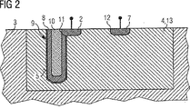
第2帯域13は、pドープ層として設けられているので、チャネル9内の第1帯域8は、nドープシリコンを有しており、第2接続パッド7のn型領域に接触接続されている。
2 第1接続パッドのp型領域
3 半導体基板
4 n型ウエル
5 pn接合
6 さらなるn型ウエル
7 第2接続パッドのn型領域
8 第1帯域
9 チャネル
10 誘電体
11 第1接触位置
12 第2接触位置
13 第2帯域
14 第3帯域
15 キャリア基板
16 埋め込み層
17 金属接続パッド
Claims (11)
- p−導電帯域およびn−導電帯域が、半導体素子の保護構造部における同じ型の電荷キャリアを有するそれぞれの領域と第1接触位置および第2接触位置において電気的に接触接続された、半導体ダイオードを少なくとも一つ有する半導体素子のESD保護構造であって、
上記半導体ダイオードの一方の電荷キャリアの型である第1帯域(8)は、上記半導体素子の半導体基板(3)内に形成されたトレンチ(9)の内部領域の少なくとも一部を覆っており、
他方の電荷キャリアの型である第2帯域(13)は、上記トレンチ付近において第1帯域(8)と隣接して形成されており、
第1帯域(8)は、適切に導電ドープされたポリシリコンによって形成されており、
該ポリシリコンによって充填されていない、空きトレンチ領域には、誘電体(10)が充填されており、
トレンチ(9)における第1のp型またはn型接触位置(11)から離れた部分に位置する第1帯域(8)の領域は、トレンチ(9)における該帯域の領域以外の領域よりも、pn接合(5)のドーピングが高ドーピングであることを特徴とする半導体素子のESD保護構造。 - トレンチの幅に対するトレンチの深さの比率は、1よりも大きいことを特徴とする請求項1に記載の半導体素子のESD保護構造。
- トレンチ(9)全体はポリシリコンにて充填されていることを特徴とする請求項1または2に記載の半導体素子のESD保護構造。
- 第1帯域(8)は、少なくともトレンチ(9)の下部領域においてトレンチ(9)の内部領域を覆っており、
第2帯域(13)は、埋め込み層(16)として、第1帯域(8)に隣接するように形成されていることを特徴とする請求項1から3のいずれか1項に記載の半導体素子のESD保護構造。 - 第2の接触領域(12)は、第3帯域(14)によって統合されており、
第3帯域(14)は、
第2帯域(13)と電荷キャリアの型が一致しており、
第2帯域(13)、および、半導体素子の保護構造部の同じ電荷キャリアの型を有する領域と、互いに電気的、導電的に隣接していることを特徴とする請求項4に記載の半導体素子のESD保護構造。 - 第1帯域(8)は、トレンチ(9)の内部領域全体を覆っており、
第2帯域(13)は、埋め込み層(16)としてトレンチ(9)の下部領域に隣接して形成されており、
この埋め込み層(16)上には第3帯域(14)として後に続く層から電気的に絶縁するさらなる層が配置され、
このさらなる層は、第2帯域(13)と電荷キャリアの型が同じであり、第2のp型またはn型接触位置(12)を形成していることを特徴とする請求項1から4のいずれか1項に記載の半導体素子のESD保護構造。 - 第3帯域(14)は、第2帯域(13)とドーピング量が異なっていることを特徴とする請求項5または6に記載の半導体素子のESD保護構造。
- トレンチ(9)は、広範囲に幾何学的な広がり、特に、細長形状、湾曲形状、または、または円形状を有していることを特徴とする請求項1から7のいずれか1項に記載の半導体素子のESD保護構造。
- 少なくとも2つの半導体ダイオードから形成されていることを特徴とする請求項1から8のいずれか1項に記載の半導体素子のESD保護構造。
- 半導体素子の保護構造部は、入出力パッドであることを特徴とする請求項1から9のいずれか1項に記載の半導体素子のESD保護構造。
- 第1帯域(8)のポリシリコンは、電気的、導電的、直接的に、金属接続パッド(17)に隣接していることを特徴とする請求項10に記載の半導体素子のESD保護構造。
Applications Claiming Priority (3)
| Application Number | Priority Date | Filing Date | Title |
|---|---|---|---|
| DE102004026100A DE102004026100B4 (de) | 2004-05-25 | 2004-05-25 | ESD-Schutzstrukturen für Halbleiterbauelemente |
| DE102004026100.8 | 2004-05-25 | ||
| PCT/DE2005/000896 WO2005117133A2 (de) | 2004-05-25 | 2005-05-17 | Esd-schutzstrukturen für halbleiterbauelemente |
Publications (2)
| Publication Number | Publication Date |
|---|---|
| JP2007538390A JP2007538390A (ja) | 2007-12-27 |
| JP4854663B2 true JP4854663B2 (ja) | 2012-01-18 |
Family
ID=35124380
Family Applications (1)
| Application Number | Title | Priority Date | Filing Date |
|---|---|---|---|
| JP2007516955A Expired - Fee Related JP4854663B2 (ja) | 2004-05-25 | 2005-05-17 | 半導体素子のesd保護構造 |
Country Status (6)
| Country | Link |
|---|---|
| US (1) | US7943928B2 (ja) |
| JP (1) | JP4854663B2 (ja) |
| CN (1) | CN1998090B (ja) |
| DE (1) | DE102004026100B4 (ja) |
| TW (1) | TW200603376A (ja) |
| WO (1) | WO2005117133A2 (ja) |
Families Citing this family (4)
| Publication number | Priority date | Publication date | Assignee | Title |
|---|---|---|---|---|
| WO2008099317A1 (en) * | 2007-02-12 | 2008-08-21 | Nxp B.V. | Esd-protection device, a semiconductor device and an integrated system in a package comprising such a device |
| US7700977B2 (en) * | 2007-06-21 | 2010-04-20 | Intersil Americas Inc. | Integrated circuit with a subsurface diode |
| US7585705B2 (en) * | 2007-11-29 | 2009-09-08 | Alpha & Omega Semiconductor, Inc. | Method for preventing gate oxide damage of a trench MOSFET during wafer processing while adding an ESD protection module atop |
| US8080851B2 (en) * | 2008-08-29 | 2011-12-20 | International Business Machines Corporation | Deep trench electrostatic discharge (ESD) protect diode for silicon-on-insulator (SOI) devices |
Citations (4)
| Publication number | Priority date | Publication date | Assignee | Title |
|---|---|---|---|---|
| JPH01191472A (ja) * | 1988-01-26 | 1989-08-01 | Fujitsu Ltd | 静電破壊防止用素子 |
| JPH06204407A (ja) * | 1992-12-28 | 1994-07-22 | Nippon Steel Corp | ダイオード素子 |
| JPH0758286A (ja) * | 1993-08-10 | 1995-03-03 | Nissan Motor Co Ltd | 半導体装置の保護回路 |
| US6710418B1 (en) * | 2002-10-11 | 2004-03-23 | Fairchild Semiconductor Corporation | Schottky rectifier with insulation-filled trenches and method of forming the same |
Family Cites Families (10)
| Publication number | Priority date | Publication date | Assignee | Title |
|---|---|---|---|---|
| US5477078A (en) * | 1994-02-18 | 1995-12-19 | Analog Devices, Incorporated | Integrated circuit (IC) with a two-terminal diode device to protect metal-oxide-metal capacitors from ESD damage |
| JP3287269B2 (ja) * | 1997-06-02 | 2002-06-04 | 富士電機株式会社 | ダイオードとその製造方法 |
| DE19740195C2 (de) * | 1997-09-12 | 1999-12-02 | Siemens Ag | Halbleiterbauelement mit Metall-Halbleiterübergang mit niedrigem Sperrstrom |
| EP0905781A3 (de) * | 1997-09-30 | 2000-11-02 | Siemens Aktiengesellschaft | ESD-Schutzdiode |
| US6448865B1 (en) * | 1999-02-25 | 2002-09-10 | Formfactor, Inc. | Integrated circuit interconnect system |
| JP4016595B2 (ja) * | 2000-12-12 | 2007-12-05 | サンケン電気株式会社 | 半導体装置及びその製造方法 |
| US6657256B2 (en) * | 2001-05-22 | 2003-12-02 | General Semiconductor, Inc. | Trench DMOS transistor having a zener diode for protection from electro-static discharge |
| US6989572B2 (en) * | 2003-07-09 | 2006-01-24 | Semiconductor Components Industries, L.L.C. | Symmetrical high frequency SCR structure |
| TWI361490B (en) * | 2003-09-05 | 2012-04-01 | Renesas Electronics Corp | A semiconductor device and a method of manufacturing the same |
| US7098509B2 (en) * | 2004-01-02 | 2006-08-29 | Semiconductor Components Industries, L.L.C. | High energy ESD structure and method |
-
2004
- 2004-05-25 DE DE102004026100A patent/DE102004026100B4/de not_active Expired - Fee Related
-
2005
- 2005-05-17 JP JP2007516955A patent/JP4854663B2/ja not_active Expired - Fee Related
- 2005-05-17 WO PCT/DE2005/000896 patent/WO2005117133A2/de active Application Filing
- 2005-05-17 CN CN2005800166487A patent/CN1998090B/zh not_active Expired - Fee Related
- 2005-05-18 TW TW094116191A patent/TW200603376A/zh not_active IP Right Cessation
-
2006
- 2006-11-21 US US11/603,340 patent/US7943928B2/en not_active Expired - Fee Related
Patent Citations (4)
| Publication number | Priority date | Publication date | Assignee | Title |
|---|---|---|---|---|
| JPH01191472A (ja) * | 1988-01-26 | 1989-08-01 | Fujitsu Ltd | 静電破壊防止用素子 |
| JPH06204407A (ja) * | 1992-12-28 | 1994-07-22 | Nippon Steel Corp | ダイオード素子 |
| JPH0758286A (ja) * | 1993-08-10 | 1995-03-03 | Nissan Motor Co Ltd | 半導体装置の保護回路 |
| US6710418B1 (en) * | 2002-10-11 | 2004-03-23 | Fairchild Semiconductor Corporation | Schottky rectifier with insulation-filled trenches and method of forming the same |
Also Published As
| Publication number | Publication date |
|---|---|
| CN1998090B (zh) | 2010-09-08 |
| CN1998090A (zh) | 2007-07-11 |
| DE102004026100B4 (de) | 2007-10-25 |
| WO2005117133A3 (de) | 2006-04-20 |
| US7943928B2 (en) | 2011-05-17 |
| WO2005117133A2 (de) | 2005-12-08 |
| TW200603376A (en) | 2006-01-16 |
| TWI303871B (ja) | 2008-12-01 |
| US20080035924A1 (en) | 2008-02-14 |
| DE102004026100A1 (de) | 2006-01-26 |
| JP2007538390A (ja) | 2007-12-27 |
Similar Documents
| Publication | Publication Date | Title |
|---|---|---|
| CN101681909B (zh) | 垂直电流受控绝缘体上硅(soi)器件及其形成方法 | |
| US7098509B2 (en) | High energy ESD structure and method | |
| US8466489B2 (en) | Apparatus and method for transient electrical overstress protection | |
| US8525299B2 (en) | Electrical overstress protection using through-silicon-via (TSV) | |
| CN101847663B (zh) | 一种瞬间电压抑制器及形成瞬间电压抑制器的方法 | |
| US5477078A (en) | Integrated circuit (IC) with a two-terminal diode device to protect metal-oxide-metal capacitors from ESD damage | |
| US7939905B2 (en) | Electrostatic discharge protection method and device for semiconductor device including an electrostatic discharge protection element providing a discharge path of a surge current | |
| US7888703B2 (en) | ESD protection apparatus and electrical circuit including same | |
| US20020028522A1 (en) | Electrostatic discharge protection device having a graded junction and method for forming the same | |
| US6747294B1 (en) | Guard ring structure for reducing crosstalk and latch-up in integrated circuits | |
| US7064358B2 (en) | Triggered back-to-back diodes for ESD protection in triple-well CMOS process | |
| KR100369496B1 (ko) | 정전방전으로부터보호하기위한구조물을가진집적반도체회로 | |
| US20240030218A1 (en) | Lateral high voltage scr with integrated negative strike diode | |
| US10672758B2 (en) | Electrostatic discharge protection structure, method for manufacturing an electrostatic discharge protection structure, and vertical thyristor structure | |
| US10269898B2 (en) | Surrounded emitter bipolar device | |
| US7943928B2 (en) | ESD protection structures for semiconductor components | |
| US20230307438A1 (en) | Electro-static discharge protection devices having a low trigger voltage | |
| US6392276B1 (en) | Device for protecting an SOI structure | |
| JP4479041B2 (ja) | 半導体装置及びその製造方法 | |
| US7053452B2 (en) | Metal oxide semiconductor device for electrostatic discharge protection circuit | |
| KR20240041724A (ko) | 정전기 방전 소자 및 이를 포함하는 디스플레이 구동 칩 |
Legal Events
| Date | Code | Title | Description |
|---|---|---|---|
| A131 | Notification of reasons for refusal |
Free format text: JAPANESE INTERMEDIATE CODE: A131 Effective date: 20101221 |
|
| TRDD | Decision of grant or rejection written | ||
| A01 | Written decision to grant a patent or to grant a registration (utility model) |
Free format text: JAPANESE INTERMEDIATE CODE: A01 Effective date: 20111004 |
|
| A01 | Written decision to grant a patent or to grant a registration (utility model) |
Free format text: JAPANESE INTERMEDIATE CODE: A01 |
|
| A61 | First payment of annual fees (during grant procedure) |
Free format text: JAPANESE INTERMEDIATE CODE: A61 Effective date: 20111025 |
|
| FPAY | Renewal fee payment (event date is renewal date of database) |
Free format text: PAYMENT UNTIL: 20141104 Year of fee payment: 3 |
|
| R150 | Certificate of patent or registration of utility model |
Ref document number: 4854663 Country of ref document: JP Free format text: JAPANESE INTERMEDIATE CODE: R150 Free format text: JAPANESE INTERMEDIATE CODE: R150 |
|
| R250 | Receipt of annual fees |
Free format text: JAPANESE INTERMEDIATE CODE: R250 |
|
| R250 | Receipt of annual fees |
Free format text: JAPANESE INTERMEDIATE CODE: R250 |
|
| R250 | Receipt of annual fees |
Free format text: JAPANESE INTERMEDIATE CODE: R250 |
|
| R250 | Receipt of annual fees |
Free format text: JAPANESE INTERMEDIATE CODE: R250 |
|
| R250 | Receipt of annual fees |
Free format text: JAPANESE INTERMEDIATE CODE: R250 |
|
| R250 | Receipt of annual fees |
Free format text: JAPANESE INTERMEDIATE CODE: R250 |
|
| LAPS | Cancellation because of no payment of annual fees |