JP4854663B2 - ESD protection structure of semiconductor element - Google Patents
ESD protection structure of semiconductor element Download PDFInfo
- Publication number
- JP4854663B2 JP4854663B2 JP2007516955A JP2007516955A JP4854663B2 JP 4854663 B2 JP4854663 B2 JP 4854663B2 JP 2007516955 A JP2007516955 A JP 2007516955A JP 2007516955 A JP2007516955 A JP 2007516955A JP 4854663 B2 JP4854663 B2 JP 4854663B2
- Authority
- JP
- Japan
- Prior art keywords
- zone
- esd protection
- protection structure
- region
- trench
- Prior art date
- Legal status (The legal status is an assumption and is not a legal conclusion. Google has not performed a legal analysis and makes no representation as to the accuracy of the status listed.)
- Expired - Fee Related
Links
- 239000004065 semiconductor Substances 0.000 title claims description 70
- 239000002800 charge carrier Substances 0.000 claims description 17
- 229910021420 polycrystalline silicon Inorganic materials 0.000 claims description 13
- 229920005591 polysilicon Polymers 0.000 claims description 13
- 239000000758 substrate Substances 0.000 claims description 12
- 230000001681 protective effect Effects 0.000 claims description 7
- 239000002184 metal Substances 0.000 claims description 4
- 230000015556 catabolic process Effects 0.000 description 12
- 238000010586 diagram Methods 0.000 description 5
- 230000003071 parasitic effect Effects 0.000 description 5
- VYPSYNLAJGMNEJ-UHFFFAOYSA-N Silicium dioxide Chemical compound O=[Si]=O VYPSYNLAJGMNEJ-UHFFFAOYSA-N 0.000 description 3
- 230000006378 damage Effects 0.000 description 3
- 238000004519 manufacturing process Methods 0.000 description 3
- 238000000034 method Methods 0.000 description 3
- XUIMIQQOPSSXEZ-UHFFFAOYSA-N Silicon Chemical compound [Si] XUIMIQQOPSSXEZ-UHFFFAOYSA-N 0.000 description 2
- 230000035945 sensitivity Effects 0.000 description 2
- 229910052710 silicon Inorganic materials 0.000 description 2
- 239000010703 silicon Substances 0.000 description 2
- 239000007858 starting material Substances 0.000 description 2
- 230000001133 acceleration Effects 0.000 description 1
- 238000009825 accumulation Methods 0.000 description 1
- 230000007423 decrease Effects 0.000 description 1
- 238000000151 deposition Methods 0.000 description 1
- 230000000994 depressogenic effect Effects 0.000 description 1
- 230000000694 effects Effects 0.000 description 1
- 238000005530 etching Methods 0.000 description 1
- 230000002349 favourable effect Effects 0.000 description 1
- 238000002513 implantation Methods 0.000 description 1
- 238000002347 injection Methods 0.000 description 1
- 239000007924 injection Substances 0.000 description 1
- 230000010354 integration Effects 0.000 description 1
- 239000000463 material Substances 0.000 description 1
- 235000012239 silicon dioxide Nutrition 0.000 description 1
- 239000000377 silicon dioxide Substances 0.000 description 1
- 229910052814 silicon oxide Inorganic materials 0.000 description 1
Images


Classifications
-
- H—ELECTRICITY
- H01—ELECTRIC ELEMENTS
- H01L—SEMICONDUCTOR DEVICES NOT COVERED BY CLASS H10
- H01L27/00—Devices consisting of a plurality of semiconductor or other solid-state components formed in or on a common substrate
- H01L27/02—Devices consisting of a plurality of semiconductor or other solid-state components formed in or on a common substrate including semiconductor components specially adapted for rectifying, oscillating, amplifying or switching and having at least one potential-jump barrier or surface barrier; including integrated passive circuit elements with at least one potential-jump barrier or surface barrier
- H01L27/0203—Particular design considerations for integrated circuits
- H01L27/0248—Particular design considerations for integrated circuits for electrical or thermal protection, e.g. electrostatic discharge [ESD] protection
- H01L27/0251—Particular design considerations for integrated circuits for electrical or thermal protection, e.g. electrostatic discharge [ESD] protection for MOS devices
- H01L27/0255—Particular design considerations for integrated circuits for electrical or thermal protection, e.g. electrostatic discharge [ESD] protection for MOS devices using diodes as protective elements
-
- H—ELECTRICITY
- H01—ELECTRIC ELEMENTS
- H01L—SEMICONDUCTOR DEVICES NOT COVERED BY CLASS H10
- H01L29/00—Semiconductor devices adapted for rectifying, amplifying, oscillating or switching, or capacitors or resistors with at least one potential-jump barrier or surface barrier, e.g. PN junction depletion layer or carrier concentration layer; Details of semiconductor bodies or of electrodes thereof ; Multistep manufacturing processes therefor
- H01L29/66—Types of semiconductor device ; Multistep manufacturing processes therefor
- H01L29/86—Types of semiconductor device ; Multistep manufacturing processes therefor controllable only by variation of the electric current supplied, or only the electric potential applied, to one or more of the electrodes carrying the current to be rectified, amplified, oscillated or switched
- H01L29/861—Diodes
Description
本発明は、少なくとも一つの半導体ダイオードを有する、半導体素子のESD保護構造に関するものである。この半導体ダイオードは、p−導電帯域およびn−導電帯域が、半導体素子の保護構造部の同じ型の電荷キャリアを有するそれぞれの領域と第1接触位置および第2接触位置において電気的に接触接続されている。 The present invention relates to an ESD protection structure for a semiconductor device having at least one semiconductor diode. In this semiconductor diode, the p-conduction band and the n-conduction band are electrically contact-connected at the first contact position and the second contact position with the respective regions having the same type of charge carriers of the protective structure of the semiconductor element. ing.
このタイプの構造は、寄生容量の影響で生じる静電気放電の不制御によるダメージまたは破壊から半導体素子を保護する。寄生容量は、保護構造を通じた所望の方式、および低抵抗方式において供給線の一つへ導電された電気充電の蓄積により生じる。これは、数アンペアの放電電流による素子のアバランシェ降伏、および素子の破壊を防止することができる。また、ESD保護構造は、破壊すること無しに必要な通電容量を半導体素子へ与えることができる寸法を有している。 This type of structure protects the semiconductor element from damage or destruction due to uncontrolled electrostatic discharge caused by parasitic capacitance. Parasitic capacitance results from the accumulation of electrical charge conducted to one of the supply lines in the desired manner through the protective structure and in a low resistance manner. This can prevent device avalanche breakdown and device breakdown due to discharge currents of several amperes. In addition, the ESD protection structure has a dimension that can provide the semiconductor element with a necessary current carrying capacity without being destroyed.
集積密度が大きくなるにつれて、だんだん小さくなっている半導体構造は、静電気容量に対する素子の感度が増している。特に、微細化に伴うMOS素子のゲート酸化物の薄型化は、半導体素子の信号入力および信号出力の感度を高める。これは、例えば、ゲート酸化物領域の破壊は、ゲート酸化物の電子の注入、および、上記放電電流の場合に素子の破壊を必然的に引き起こすチャネルの電荷キャリアの加速と関連しているためである。 As the integration density increases, the increasingly smaller semiconductor structure increases the sensitivity of the device to electrostatic capacitance. In particular, the thinning of the gate oxide of the MOS element accompanying the miniaturization increases the sensitivity of signal input and signal output of the semiconductor element. This is because, for example, the breakdown of the gate oxide region is associated with the injection of electrons in the gate oxide and the acceleration of channel charge carriers, which inevitably causes device breakdown in the case of the above discharge current. is there.
電荷の所望のバイパスによって素子の保護をもたらす、ESD保護構造のよく知られた実施の形態では、半導体構造内にダイオードを設けている。この場合、ダイオードの降伏電圧を、半導体素子の保護構造の降伏電圧よりも低くすることができる。このダイオードは、基板の表面付近の領域のp型およびn型にドープされた領域に対応して形成される。降伏は、互いに垂直方向または側面方向に隣接した領域のエリアで起こる。この場合、ESD保護構造の内部抵抗は、重要な要素である。このようなダイオードは、一般的に、非常に大きな寄生直列抵抗を持っている。この寄生直接抵抗は、短絡に至る電流量をかなり制限する。pn整合部のアクティブエリアを拡張する、例えばダイオードに大きなエリアを持たせることによって、該ダイオードの内部抵抗を減らすことができる。しかしながら、入力回路の静電容量(キャパシタンス)を増やすと共に、素子のチップ密度を減らすだけでなく、半導体素子全体にかかるコストがアップする。 In a well-known embodiment of an ESD protection structure that provides protection of the device by the desired bypass of charge, a diode is provided in the semiconductor structure. In this case, the breakdown voltage of the diode can be made lower than the breakdown voltage of the protective structure of the semiconductor element. This diode is formed corresponding to the p-type and n-type doped regions in the region near the surface of the substrate. Yield occurs in areas of areas adjacent to each other in the vertical or lateral direction. In this case, the internal resistance of the ESD protection structure is an important factor. Such diodes generally have a very large parasitic series resistance. This parasitic direct resistance considerably limits the amount of current leading to a short circuit. By expanding the active area of the pn matching portion, for example, by providing a large area for the diode, the internal resistance of the diode can be reduced. However, not only the capacitance (capacitance) of the input circuit is increased and the chip density of the device is reduced, but also the cost of the entire semiconductor device is increased.
表面付近の領域に注入することによって、EDS保護構造を実現する場合、シリコン表面付近に流れる電流は、局所的な温度上昇をもたらし、さらに、通電容量が減少し、さらに、局所的に高温の場合に、素子に対するダメージが大きくなる。 When an EDS protection structure is realized by injecting into a region near the surface, the current flowing near the silicon surface brings about a local temperature rise, and further, the current carrying capacity is reduced. In addition, the damage to the element is increased.
従って、本発明は、少なくとも要求されるスペースと同程度のスペースを有する、または、少なくとも要求されるスペースよりも小さいスペースと同程度の通電容量を有すると同時に、より高い通電容量を得ることができ、かつ、低コストのESD保護構造を提供することを目的とする。 Therefore, the present invention has at least the same space as the required space, or at least the same current capacity as the space smaller than the required space, and at the same time can obtain a higher current capacity. And it aims at providing a low-cost ESD protection structure.
本発明によれば、上記半導体ダイオードの一方の電荷キャリア型である第1帯域は、上記半導体素子の半導体基板内に形成されたチャネルの内部領域の少なくとも一部を覆っており、他方の電荷キャリアの型である第2帯域は、上記チャネル付近において第1帯域と隣接して形成されており、第1帯域は、適切に導電ドープされたポリシリコンによって形成されており、該ポリシリコンによって充填されていない、空きチャネル領域には、誘電体が充填されている。 According to the present invention, one charge carrier type first band of the semiconductor diode covers at least a part of an inner region of a channel formed in the semiconductor substrate of the semiconductor element, and the other charge carrier. The second zone of the type is formed adjacent to the first zone in the vicinity of the channel, and the first zone is formed by appropriately conductively doped polysilicon and is filled with the polysilicon. The empty channel region not filled is filled with a dielectric.
上記ESD保護構造のチャネル型の形態では、第1電荷キャリア型の帯域を第2の電荷キャリア型の帯域に少なくとも部分的に落ち込ませることができる。pn接合のアクティブ領域は、必要なチップ領域に対して十分に大きく、ESD保護構造の通電容量は、同程度増える。この場合、pn接合のアクティブ領域のサイズは、最大でチャネルの横領域全体のサイズまで、ESD保護構造に応じてかなりフレキシブルに設定することができる。 In the channel type configuration of the ESD protection structure, the first charge carrier type band can be at least partially depressed into the second charge carrier type band. The active region of the pn junction is sufficiently larger than the necessary chip region, and the current carrying capacity of the ESD protection structure increases to the same extent. In this case, the size of the active region of the pn junction can be set quite flexibly depending on the ESD protection structure up to the size of the entire lateral region of the channel.
チャネルの深さがチャネルの幅よりも大きい場合、ESD保護構造に必要なチップ領域と、pn接合のアクティブ領域との間の比率は、かなり好適な比率となり、高い通電容量を持つESD保護構造はとても効果的にすることができ、特に有利な形態を提供することができる。この場合、pn接合は、ESD保護構造の形状に依存して、pn接合とnp接合の両方を含んでいる。 When the channel depth is larger than the channel width, the ratio between the chip area required for the ESD protection structure and the active area of the pn junction is a fairly favorable ratio, and the ESD protection structure with high current carrying capacity is It can be very effective and can provide a particularly advantageous form. In this case, the pn junction includes both a pn junction and an np junction depending on the shape of the ESD protection structure.
チャネル内の半導体ダイオードとして試験済みのESD保護構造、いわゆる、トレンチプロセスモジュールの形態では、所望の第1帯域の生成によって、チャネルの内部領域を少なくとも部分的に覆うことを可能にしている。上記第1帯域は、保護すべき半導体素子のタイプによって、p−導電またはn−導電とすることができる。p−導電としての第1帯域の構成は、標準形態として用いることができ、n−導電としての第1の帯域の構成により、例えば、いろいろなタイプのCMOS素子の保護など、多数を加えることができる。 In the form of an ESD protection structure that has been tested as a semiconductor diode in the channel, the so-called trench process module, it is possible to at least partially cover the inner region of the channel by the generation of the desired first band. The first zone may be p-conductive or n-conductive depending on the type of semiconductor element to be protected. The configuration of the first band as p-conductivity can be used as a standard form, and the configuration of the first band as n-conductivity can add many, for example, protection of various types of CMOS devices. it can.
本発明によれば、チャネルの内部領域は、少なくとも部分的に、第1帯域にて覆われている。第1帯域と、半導体素子の保護構造部と同じ型の電荷キャリアの領域と、間での電気的な接触(ここでは第1の接触位置と称する)が、ESDの場合に、電荷が上記第1接触位置を通してバイパスでの迂回を確実にするために実現されている限り、原理上、チャネルは、異なる材料にて充填された部分を含んでいる。しかしながら、概略的には、チャネルの内部領域全体は、第1帯域に覆われている。 According to the invention, the inner region of the channel is at least partially covered by the first zone. When electrical contact (referred to herein as a first contact position) between the first zone and a region of charge carriers of the same type as the protection structure portion of the semiconductor element is ESD, the charge is In principle, the channel includes portions filled with different materials, as long as it is realized to ensure bypass bypassing through one contact location. In general, however, the entire interior region of the channel is covered by the first zone.
pnまたはnp半導体ダイオードは、第1および第2帯域のドーピングによって形成される。この場合、特に、第2帯域は、保護のための半導体素子のウエルによって形成され、これによって、第2帯域のドーピングが規定される。チャネルが形成された第2帯域は、例えば、半導体素子のn型ウエルとしてもよい。これにより、第1帯域は、p−導電型にドープされたポリシリコンによって形成することができる。 A pn or np semiconductor diode is formed by doping in the first and second bands. In this case, in particular, the second zone is formed by a well of a semiconductor element for protection, which defines the doping of the second zone. The second band in which the channel is formed may be, for example, an n-type well of a semiconductor element. Thereby, the first zone can be formed by polysilicon doped to p-type conductivity.
半導体素子の既存の基板を第2帯域として用いるか、または、第2帯域を積極的に半導体基板に形成するかは、個々のケース、半導体素子の構造および生成された通電容量に依存している。 Whether the existing substrate of the semiconductor element is used as the second band or whether the second band is actively formed on the semiconductor substrate depends on the individual case, the structure of the semiconductor element, and the generated current carrying capacity. .
本発明によれば、第1のゾーンとしてポリシリコンを用いており、ESD保護構造のpn接合は、非常に低抵抗と接続される。従って、チャネル内の第1帯域の直列抵抗は、pn接合の抵抗よりも低くなり、その結果、チャネル内のより深くに位置するダイオード領域全体にダイオード降伏が同時に生じる。このように、半導体素子を保護する通電容量は、pn接合のアクティブ領域全体によって規定され、この領域を生成する方法技術によって直接的に決めることができる。 According to the present invention, polysilicon is used as the first zone, and the pn junction of the ESD protection structure is connected to a very low resistance. Accordingly, the series resistance of the first band in the channel is lower than the resistance of the pn junction, and as a result, diode breakdown occurs simultaneously in the entire deeper diode region in the channel. As described above, the current carrying capacity for protecting the semiconductor element is defined by the entire active region of the pn junction, and can be directly determined by a method technique for generating this region.
上記事実によれば、特に本発明の有利な構成は、チャネルにおける第1のp型またはn型接触位置から離れた部分に位置する第1帯域の領域は、チャネルにおける該帯域の領域以外の領域よりも、pn接合のドーピングが高ドーピングとなっていることである。第1の降伏の位置は、所望の方式においてチャネルの下方領域へとシフトする。チャネルの内部抵抗の全域の電圧降下は、その後、降伏がチャネルの上方領域で生じるという効果を生む。 According to the above fact, particularly advantageous configuration of the present invention is that the region of the first band located in the channel away from the first p-type or n-type contact position is a region other than the region of the band in the channel. Rather, the pn junction is highly doped. The position of the first breakdown shifts to the lower region of the channel in the desired manner. The voltage drop across the internal resistance of the channel then has the effect that breakdown occurs in the upper region of the channel.
ポリシリコンにて充填されていないチャネルの領域は、例えば酸化珪素などの誘電体が一様に充填されている。半導体素子の保護構造部と同じ型の電荷キャリアの領域、例えば、p導電第1帯域の場合、p導電領域が、部分的に第1帯域と重なり、寄生容量がこれらの接合部分を通じて導電することによって、第1の接触領域が形成されている。 The channel region not filled with polysilicon is uniformly filled with a dielectric such as silicon oxide. In the case of a charge carrier region of the same type as the protective structure portion of the semiconductor element, for example, in the p-conducting first band, the p-conducting region partially overlaps the first band, and the parasitic capacitance is conducted through these junctions. Thus, the first contact region is formed.
本発明のさらに他の構成において、チャネル全体がポリシリコンによって充填されていれば、第1の接触位置は、さらにフレキシブルに設計することができ、かつ、接合部分は、完全に重なった場合、最大となる。この構成は、半導体素子の構造によれば、導電させる期待電流および第1接触位置を生成する可能性に従って用いられる。 In yet another configuration of the present invention, if the entire channel is filled with polysilicon, the first contact location can be designed to be more flexible, and if the joint is fully overlapped, It becomes. This configuration is used according to the structure of the semiconductor element according to the expected current to be conducted and the possibility of generating the first contact position.
上記の通り、原理上は、チャネルを第1帯域としてのポリシリコンを用いて充填することによって、pn接合を能動(アクティブ)領域とすることができる。しかし、第1帯域に近接した第2帯域の形状およびサイズの構成によってさらに費用効率を高めることができる。 As described above, in principle, the pn junction can be made an active region by filling the channel with polysilicon as the first band. However, cost efficiency can be further enhanced by the configuration of the shape and size of the second zone proximate to the first zone.
本発明のさらなる構成、通電容量を必要とする構成によれば、第1帯域が少なくともチャネルの下部領域においてチャネルの内部領域を覆っている場合、第2帯域を埋め込み層として形成することができる。また、埋め込み層が半導体素子の保護構造部と同じ型の電荷キャリアを有する領域と電気的に接触していない場合、この場合、第2接触位置は、第3帯域によって統合されている。第3帯域は、第2帯域と同じ電荷キャリアの型を有しており、第2帯域と電気的、導電的に隣接している。 According to the further configuration of the present invention and the configuration requiring current carrying capacity, the second band can be formed as a buried layer when the first band covers the channel inner region at least in the lower region of the channel. Also, if the buried layer is not in electrical contact with a region having the same type of charge carrier as the protective structure of the semiconductor element, in this case, the second contact position is integrated by the third zone. The third zone has the same charge carrier type as the second zone and is electrically and conductively adjacent to the second zone.
ところで、上記の埋め込み層は、ESD保護構造として、半導体素子に用いられている層である。しかしながら、ESD保護構造のために、特別に埋め込まれたウエルによって第2帯域を得ることができる。これは、半導体ダイオードの降伏を、pn接合のドーピングによって、狙い通りに行うことができる、という利点がある。 By the way, the buried layer is a layer used for a semiconductor element as an ESD protection structure. However, due to the ESD protection structure, the second zone can be obtained by a specially buried well. This has the advantage that the breakdown of the semiconductor diode can be performed as intended by doping the pn junction.
さらに、他の例では、第1帯域は、チャネルの内部領域全体を覆っており、第2帯域は、埋め込み層としてチャネルの下部領域に隣接して形成されており、この埋め込み層上には第3帯域として後に続く層から電気的に絶縁するさらなる層が配置され、このさらなる層は、第2帯域と電荷キャリアの型が同じであり、第2のp型またはn型接触位置を形成しているものを提供することができる。この特徴を有する構造は、素子構造に現在利用されているBiCMOS素子のESD保護構造に適している。 Further, in another example, the first band covers the entire inner region of the channel, and the second band is formed as a buried layer adjacent to the lower region of the channel, and the second band is formed on the buried layer. A further layer is arranged that is electrically isolated from the following layers as three zones, which are of the same charge carrier type as the second zone and form a second p-type or n-type contact location. Can provide what is. The structure having this characteristic is suitable for the ESD protection structure of the BiCMOS element currently used for the element structure.
さらに、第3帯域のドーピング量と第2帯域のドーピング量とを互いに異ならせることによって、電荷の損失調整およびpn接合のドーピングを狙い通りにすることができる。 Further, by adjusting the doping amount of the third band and the doping amount of the second band to be different from each other, the charge loss adjustment and the pn junction doping can be achieved as intended.
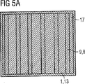
導入部に記載したように、pn接合のアクティブ領域が増えるに従って、ESD保護構造の通電容量が増えて、半導体ダイオードの内部抵抗は小さくなる。特に、本発明の有利な構成では、チャネルは、広範囲に幾何学的な範囲を有しており、特に、細長形状(form of strips)、湾曲形状、または、または円形状を有している。 As described in the introduction part, as the active region of the pn junction increases, the current carrying capacity of the ESD protection structure increases and the internal resistance of the semiconductor diode decreases. In particular, in an advantageous configuration of the invention, the channels have a wide geometric range, in particular have a form of strips, a curved shape or a circular shape.
チャネル形状の生成は、半導体ダイオードおよび降伏領域の形状とを規定するため、ESD保護構造を形成するために利用可能なスペースに依存して、最適な接合領域を形成するのと同様に、チャネル形状を規定することができる。また、ESD構造では、2つまたはそれ以上の半導体ダイオードを含めることができる。一例として、半導体素子の保護構造部を入出力パッドとした場合、例えば、平行な細長形状、曲線形状、円形状のパッドの下の半導体ダイオードの配置は、とても効率的なものにすることができる。 The generation of the channel shape defines the shape of the semiconductor diode and the breakdown region, so depending on the space available to form the ESD protection structure, the channel shape is similar to forming the optimum junction region. Can be defined. An ESD structure can also include two or more semiconductor diodes. As an example, when the protection structure portion of the semiconductor element is an input / output pad, for example, the arrangement of the semiconductor diode under the parallel elongated, curved, or circular pad can be made very efficient. .
第1帯域のポリシリコンは、電気的、伝導的、直接的に、金属接続パッドと隣接している。 The first zone polysilicon is electrically, conductively and directly adjacent to the metal connection pads.
本発明について、以下に示すより詳細な実施の形態の説明を基に説明する。 The present invention will be described based on the following detailed description of embodiments.
図1abは、従来技術としてのESD保護ダイオードを示す概略図である。 FIG. 1ab is a schematic diagram showing a conventional ESD protection diode.
図2は、本発明のESD保護構造を示す概略図である。 FIG. 2 is a schematic diagram illustrating the ESD protection structure of the present invention.
図3は、埋め込み層を有するESD保護構造の実施の形態を示す概略図である。 FIG. 3 is a schematic diagram illustrating an embodiment of an ESD protection structure having a buried layer.
図4は、BiCMOSのESD保護構造を示す概略図である。 FIG. 4 is a schematic diagram showing a BiCMOS ESD protection structure.
図5abは、それぞれESD保護構造の幾何学配置が異なる実施の形態を示す図である。 FIG. 5ab is a diagram showing an embodiment in which the geometry of the ESD protection structure is different.
従来技術によれば、ESD保護ダイオードは、図1abに示すように、半導体素子の入出力パッドと一体化されており、これ以上詳細な説明は開示されていない。 According to the prior art, as shown in FIG. 1ab, the ESD protection diode is integrated with the input / output pad of the semiconductor element, and no further detailed description is disclosed.
これらの図面によれば、ESD保護ダイオードは、第1接続パッド2のp型領域と電気的に接続されp導電型にドープされたウエル(p型ウエル)1と、該p型ウエル1よりも半導体基板3に相対的に深い領域に位置し、上記p型ウエル1に隣接したn導電型にドープされたウエル(n型ウエル)4と、を有している。p型ウエル1とn型ウエル4との間の接触領域には、pn接合5のアクティブ領域が形成されている。この領域のサイズは、ウエルの垂直範囲(垂直方向の範囲)、または、水平範囲(垂直方向の範囲)によって直接規定されている。pn接合5は、図1aに示す水平範囲を有しており、図1bに示す垂直範囲を有している。そのため、p型・n型ウエル1・4によって形成されたダイオードの降伏は、垂直方向(図1a)および横方向(図1b)に生じる。
According to these drawings, the ESD protection diode includes a well (p-type well) 1 that is electrically connected to the p-type region of the first connection pad 2 and is doped to a p-conductivity type. It has an n-conductivity-type well (n-type well) 4 located in a relatively deep region in the
ESDを用いた場合に蓄積される余剰電荷は、さらに別のn型ウエル6を通して、低抵抗方式(fashion)の供給線へ導電される。このn型ウエル6は、ダイオードのn型ウエル4、および、第2の接続パッド7のn型領域に電気的に接続されている。 The surplus charge stored in the case of using ESD is conducted through a further n-type well 6 to a low-resistance supply line. The n-type well 6 is electrically connected to the n-type well 4 of the diode and the n-type region of the second connection pad 7.
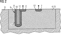
本発明のESD保護構造は、図2に示すように、上記と同様に、半導体ダイオードである。この半導体ダイオードは、n型ウエル4に取り込まれたチャネル9の内部領域を全面的に覆うp−導電第1帯域8から形成されている。チャネルにおける、p−導電第1帯域8にて覆っている部分の厚みは、チャネルの厚みの半分よりも小さい。結果として、チャネル9は、p−導電第1帯域8にて充填されておらず、空き残存領域には、二酸化珪素誘電体10が充填されている。
As shown in FIG. 2, the ESD protection structure of the present invention is a semiconductor diode as described above. This semiconductor diode is formed of a p-conducting first band 8 that covers the entire inner region of the
ところで、第1帯域8は、第1接触位置11において、第1接続パッド2のp型領域と電気的に接触している。チャネル9を完全に取り囲んでいる、半導体基板3のn型ウエル4は、第2帯域13を形成している。この第2帯域13は、同時に、第2接続パッド(第2接触位置12)7のn型領域も完全に取り囲んでいる。pn接合5のアクティブ領域は、チャネル9の外部領域によって形成されており、このpn接合5のアクティブ領域は、チャネルの内部領域と対応しており、さらに、第1帯域8と第2の帯域との接合部分によって形成されている。ESDを用いた場合、余剰電荷は、よく知られた方法によって、供給線を通して、導電される。
By the way, the first zone 8 is in electrical contact with the p-type region of the first connection pad 2 at the
このような半導体ダイオードを製造するために、半導体素子構造の製造を同時に行う。しかし、ここでは、ESD構造の製造のみに言及する。幾何学的に延びたチャネル9、または、その他の多数のチャネル9は、特に、異方性エッチングによって十分薄くされたnドープ層の開始材料によって取り囲まれている。チャネル9内にpドープされたポリシリコンを堆積させることによって、第1帯域8を所望の厚みにすることができ、その後、チャネル9に充填する酸化物層10を所望の厚みにすることができる。半導体素子の製造の途中において、接続パッド2・7のn型、p型領域をn型ウエル(開始材料)4に形成する。
In order to manufacture such a semiconductor diode, a semiconductor element structure is simultaneously manufactured. However, here we refer only to the fabrication of ESD structures. The geometrically extending
図3に示すEDS保護構造は、上記と同様に、半導体ダイオードの構成を示している。半導体ダイオードの必須の構成は図2と同じである。この実施の構成によれば、第2の帯域13は、埋め込み層16によって形成されている。この埋め込み層16は、打ち込み(implantation)によって形成されており、チャネルの下半分を取り囲んでいる。その結果、チャネルの外部領域のこの下側部分のみにおいて、チャネル9の下側領域における第1帯域8と埋め込み層16内の第2帯域13との間が、pn接合5として機能する。
The EDS protection structure shown in FIG. 3 shows the configuration of the semiconductor diode as described above. The essential configuration of the semiconductor diode is the same as in FIG. According to this embodiment, the second band 13 is formed by the buried layer 16. This buried layer 16 is formed by implantation and surrounds the lower half of the channel. As a result, only in this lower portion of the channel outer region, the pn junction 5 functions between the first band 8 in the lower region of the
供給線へ余剰電荷を導電させるための、第2接続パッド7のn型領域と第2帯域13との電気的な接触接続は、n型ウエル4として形成された第3帯域14にて実現されている。第2接触位置12は、上記第3帯域14、および、第2接続パッド7のn型領域によって形成されている。
The electrical contact connection between the n-type region of the second connection pad 7 and the second zone 13 for conducting surplus charges to the supply line is realized in the third zone 14 formed as the n-type well 4. ing. The
本発明のESD保護構造は、図4に示すように、p−導電キャリア基板15、この上に続けて設けられたp導電埋め込み層16、および、さらに、この上に続けて設けられこれらを統合するp型ウエル1によって保護される、既存のBiCMOS構造を利用することができる。本実施の形態によれば、チャネル9は、キャリア基板15に至るまで下方へ広がっている。従って、チャネル9は、p型ウエル1および埋め込み層16を貫いて延びており、第2帯域13は、これら2つの層の間で分割されている。
第2帯域13は、pドープ層として設けられているので、チャネル9内の第1帯域8は、nドープシリコンを有しており、第2接続パッド7のn型領域に接触接続されている。
As shown in FIG. 4, the ESD protection structure of the present invention includes a p-conductive carrier substrate 15, a p-conductive buried layer 16 provided on the p-conductive carrier substrate 15, and further provided on the p-conductive carrier layer 15. The existing BiCMOS structure protected by the p-type well 1 can be used. According to the present embodiment, the
Since the second band 13 is provided as a p-doped layer, the first band 8 in the
図5a・bによる本発明の典型的な実施の形態は、ESD保護構造が幾何学的な広がりが可能であることを示している。 The exemplary embodiment of the present invention according to FIGS. 5a and b shows that the ESD protection structure can be geometrically expanded.
この構造は、図5aでは、多数の平行でストリップ形状の半導体ダイオードによって形成されており、図5bでは、円形状の半導体ダイオードによって形成されている。ここでは、半導体ダイオードの可能な構造の一つを記載しているにすぎない。しかしながら、これらのESD保護構造は、接続パッド2、7のn型領域およびp型領域に、この構造を有する半導体ダイオードによって接続されているのではなく、金属接続パッド17に直接接続されている。
This structure is formed by a number of parallel, strip-shaped semiconductor diodes in FIG. 5a and by a circular semiconductor diode in FIG. 5b. Here, only one possible structure of the semiconductor diode is described. However, these ESD protection structures are not directly connected to the n-type region and the p-type region of the connection pads 2 and 7 by the semiconductor diode having this structure, but are directly connected to the
1 p型ウエル
2 第1接続パッドのp型領域
3 半導体基板
4 n型ウエル
5 pn接合
6 さらなるn型ウエル
7 第2接続パッドのn型領域
8 第1帯域
9 チャネル
10 誘電体
11 第1接触位置
12 第2接触位置
13 第2帯域
14 第3帯域
15 キャリア基板
16 埋め込み層
17 金属接続パッド
1 p-type well 2 p-type region of
Claims (11)
上記半導体ダイオードの一方の電荷キャリアの型である第1帯域(8)は、上記半導体素子の半導体基板(3)内に形成されたトレンチ(9)の内部領域の少なくとも一部を覆っており、
他方の電荷キャリアの型である第2帯域(13)は、上記トレンチ付近において第1帯域(8)と隣接して形成されており、
第1帯域(8)は、適切に導電ドープされたポリシリコンによって形成されており、
該ポリシリコンによって充填されていない、空きトレンチ領域には、誘電体(10)が充填されており、
トレンチ(9)における第1のp型またはn型接触位置(11)から離れた部分に位置する第1帯域(8)の領域は、トレンチ(9)における該帯域の領域以外の領域よりも、pn接合(5)のドーピングが高ドーピングであることを特徴とする半導体素子のESD保護構造。A semiconductor diode, wherein the p-conduction band and the n-conduction band are electrically contact-connected at the first contact position and the second contact position with respective regions having the same type of charge carrier in the protective structure of the semiconductor element. An ESD protection structure of a semiconductor element having at least one,
The first band (8), which is one charge carrier type of the semiconductor diode, covers at least a part of the inner region of the trench (9) formed in the semiconductor substrate (3) of the semiconductor element,
The second zone (13), which is the other type of charge carrier, is formed adjacent to the first zone (8) in the vicinity of the trench ,
The first zone (8) is formed by appropriately conductively doped polysilicon;
An empty trench region not filled with the polysilicon is filled with a dielectric (10) ,
The region of the first band (8) located in the portion away from the first p-type or n-type contact position (11) in the trench (9) is more than the region other than the region of the band in the trench (9). An ESD protection structure for a semiconductor device, wherein the pn junction (5) is highly doped .
第2帯域(13)は、埋め込み層(16)として、第1帯域(8)に隣接するように形成されていることを特徴とする請求項1から3のいずれか1項に記載の半導体素子のESD保護構造。 4. The semiconductor device according to claim 1, wherein the second zone is formed as a buried layer so as to be adjacent to the first zone. 8. ESD protection structure.
第3帯域(14)は、 The third band (14) is
第2帯域(13)と電荷キャリアの型が一致しており、 The second band (13) and the type of charge carrier match,
第2帯域(13)、および、半導体素子の保護構造部の同じ電荷キャリアの型を有する領域と、互いに電気的、導電的に隣接していることを特徴とする請求項4に記載の半導体素子のESD保護構造。 5. The semiconductor device according to claim 4, wherein the second zone and the region having the same charge carrier type of the protective structure of the semiconductor device are electrically and conductively adjacent to each other. 6. ESD protection structure.
第2帯域(13)は、埋め込み層(16)としてトレンチ(9)の下部領域に隣接して形成されており、 The second zone (13) is formed as a buried layer (16) adjacent to the lower region of the trench (9),
この埋め込み層(16)上には第3帯域(14)として後に続く層から電気的に絶縁するさらなる層が配置され、 On this buried layer (16) there is arranged a further layer which is electrically isolated from the subsequent layers as a third zone (14),
このさらなる層は、第2帯域(13)と電荷キャリアの型が同じであり、第2のp型またはn型接触位置(12)を形成していることを特徴とする請求項1から4のいずれか1項に記載の半導体素子のESD保護構造。 5. This further layer is of the same charge carrier type as the second zone (13) and forms a second p-type or n-type contact location (12). The ESD protection structure of the semiconductor element of any one of Claims 1.
Applications Claiming Priority (3)
| Application Number | Priority Date | Filing Date | Title |
|---|---|---|---|
| DE102004026100.8 | 2004-05-25 | ||
| DE102004026100A DE102004026100B4 (en) | 2004-05-25 | 2004-05-25 | ESD protective structures for semiconductor devices |
| PCT/DE2005/000896 WO2005117133A2 (en) | 2004-05-25 | 2005-05-17 | Esd-protection structures for semiconductor components |
Publications (2)
| Publication Number | Publication Date |
|---|---|
| JP2007538390A JP2007538390A (en) | 2007-12-27 |
| JP4854663B2 true JP4854663B2 (en) | 2012-01-18 |
Family
ID=35124380
Family Applications (1)
| Application Number | Title | Priority Date | Filing Date |
|---|---|---|---|
| JP2007516955A Expired - Fee Related JP4854663B2 (en) | 2004-05-25 | 2005-05-17 | ESD protection structure of semiconductor element |
Country Status (6)
| Country | Link |
|---|---|
| US (1) | US7943928B2 (en) |
| JP (1) | JP4854663B2 (en) |
| CN (1) | CN1998090B (en) |
| DE (1) | DE102004026100B4 (en) |
| TW (1) | TW200603376A (en) |
| WO (1) | WO2005117133A2 (en) |
Families Citing this family (4)
| Publication number | Priority date | Publication date | Assignee | Title |
|---|---|---|---|---|
| EP2130226B1 (en) | 2007-02-12 | 2012-06-06 | Nxp B.V. | ESD-protection device, a semiconductor device and an integrated system in a package comprising such a device |
| US7700977B2 (en) * | 2007-06-21 | 2010-04-20 | Intersil Americas Inc. | Integrated circuit with a subsurface diode |
| US7585705B2 (en) * | 2007-11-29 | 2009-09-08 | Alpha & Omega Semiconductor, Inc. | Method for preventing gate oxide damage of a trench MOSFET during wafer processing while adding an ESD protection module atop |
| US8080851B2 (en) | 2008-08-29 | 2011-12-20 | International Business Machines Corporation | Deep trench electrostatic discharge (ESD) protect diode for silicon-on-insulator (SOI) devices |
Citations (4)
| Publication number | Priority date | Publication date | Assignee | Title |
|---|---|---|---|---|
| JPH01191472A (en) * | 1988-01-26 | 1989-08-01 | Fujitsu Ltd | Electrostatic breakdown preventive element |
| JPH06204407A (en) * | 1992-12-28 | 1994-07-22 | Nippon Steel Corp | Diode element |
| JPH0758286A (en) * | 1993-08-10 | 1995-03-03 | Nissan Motor Co Ltd | Protective circuit of semiconductor device |
| US6710418B1 (en) * | 2002-10-11 | 2004-03-23 | Fairchild Semiconductor Corporation | Schottky rectifier with insulation-filled trenches and method of forming the same |
Family Cites Families (10)
| Publication number | Priority date | Publication date | Assignee | Title |
|---|---|---|---|---|
| US5477078A (en) * | 1994-02-18 | 1995-12-19 | Analog Devices, Incorporated | Integrated circuit (IC) with a two-terminal diode device to protect metal-oxide-metal capacitors from ESD damage |
| JP3287269B2 (en) * | 1997-06-02 | 2002-06-04 | 富士電機株式会社 | Diode and manufacturing method thereof |
| DE19740195C2 (en) * | 1997-09-12 | 1999-12-02 | Siemens Ag | Semiconductor device with metal-semiconductor junction with low reverse current |
| EP0905781A3 (en) * | 1997-09-30 | 2000-11-02 | Siemens Aktiengesellschaft | ESD protection diode |
| US6448865B1 (en) * | 1999-02-25 | 2002-09-10 | Formfactor, Inc. | Integrated circuit interconnect system |
| JP4016595B2 (en) * | 2000-12-12 | 2007-12-05 | サンケン電気株式会社 | Semiconductor device and manufacturing method thereof |
| US6657256B2 (en) * | 2001-05-22 | 2003-12-02 | General Semiconductor, Inc. | Trench DMOS transistor having a zener diode for protection from electro-static discharge |
| US6989572B2 (en) * | 2003-07-09 | 2006-01-24 | Semiconductor Components Industries, L.L.C. | Symmetrical high frequency SCR structure |
| TWI361490B (en) * | 2003-09-05 | 2012-04-01 | Renesas Electronics Corp | A semiconductor device and a method of manufacturing the same |
| US7098509B2 (en) * | 2004-01-02 | 2006-08-29 | Semiconductor Components Industries, L.L.C. | High energy ESD structure and method |
-
2004
- 2004-05-25 DE DE102004026100A patent/DE102004026100B4/en not_active Expired - Fee Related
-
2005
- 2005-05-17 WO PCT/DE2005/000896 patent/WO2005117133A2/en active Application Filing
- 2005-05-17 JP JP2007516955A patent/JP4854663B2/en not_active Expired - Fee Related
- 2005-05-17 CN CN2005800166487A patent/CN1998090B/en not_active Expired - Fee Related
- 2005-05-18 TW TW094116191A patent/TW200603376A/en not_active IP Right Cessation
-
2006
- 2006-11-21 US US11/603,340 patent/US7943928B2/en not_active Expired - Fee Related
Patent Citations (4)
| Publication number | Priority date | Publication date | Assignee | Title |
|---|---|---|---|---|
| JPH01191472A (en) * | 1988-01-26 | 1989-08-01 | Fujitsu Ltd | Electrostatic breakdown preventive element |
| JPH06204407A (en) * | 1992-12-28 | 1994-07-22 | Nippon Steel Corp | Diode element |
| JPH0758286A (en) * | 1993-08-10 | 1995-03-03 | Nissan Motor Co Ltd | Protective circuit of semiconductor device |
| US6710418B1 (en) * | 2002-10-11 | 2004-03-23 | Fairchild Semiconductor Corporation | Schottky rectifier with insulation-filled trenches and method of forming the same |
Also Published As
| Publication number | Publication date |
|---|---|
| TWI303871B (en) | 2008-12-01 |
| TW200603376A (en) | 2006-01-16 |
| JP2007538390A (en) | 2007-12-27 |
| US20080035924A1 (en) | 2008-02-14 |
| CN1998090A (en) | 2007-07-11 |
| WO2005117133A3 (en) | 2006-04-20 |
| CN1998090B (en) | 2010-09-08 |
| WO2005117133A2 (en) | 2005-12-08 |
| DE102004026100A1 (en) | 2006-01-26 |
| US7943928B2 (en) | 2011-05-17 |
| DE102004026100B4 (en) | 2007-10-25 |
Similar Documents
| Publication | Publication Date | Title |
|---|---|---|
| CN1894794B (en) | High energy ESD structure and method | |
| CN101681909B (en) | Vertical current controlled silicon on insulator (soi) device and method of forming same | |
| US8525299B2 (en) | Electrical overstress protection using through-silicon-via (TSV) | |
| US8466489B2 (en) | Apparatus and method for transient electrical overstress protection | |
| US5477078A (en) | Integrated circuit (IC) with a two-terminal diode device to protect metal-oxide-metal capacitors from ESD damage | |
| US7939905B2 (en) | Electrostatic discharge protection method and device for semiconductor device including an electrostatic discharge protection element providing a discharge path of a surge current | |
| US7888703B2 (en) | ESD protection apparatus and electrical circuit including same | |
| US20020028522A1 (en) | Electrostatic discharge protection device having a graded junction and method for forming the same | |
| US6747294B1 (en) | Guard ring structure for reducing crosstalk and latch-up in integrated circuits | |
| US7064358B2 (en) | Triggered back-to-back diodes for ESD protection in triple-well CMOS process | |
| KR100369496B1 (en) | Integrated semiconductor circuit with structure for protecting from electrostatic discharge | |
| US20220223584A1 (en) | Lateral high voltage scr with integrated negative strike diode | |
| US20180108648A1 (en) | Electrostatic Discharge Protection Structure, Method for Manufacturing an Electrostatic Discharge Protection Structure, and Vertical Thyristor Structure | |
| JP4854663B2 (en) | ESD protection structure of semiconductor element | |
| US10269898B2 (en) | Surrounded emitter bipolar device | |
| US6392276B1 (en) | Device for protecting an SOI structure | |
| US7053452B2 (en) | Metal oxide semiconductor device for electrostatic discharge protection circuit | |
| JP4479041B2 (en) | Semiconductor device and manufacturing method thereof | |
| US20230307438A1 (en) | Electro-static discharge protection devices having a low trigger voltage | |
| KR20240041724A (en) | Electrostatic discharge device and display drive chip including the same |
Legal Events
| Date | Code | Title | Description |
|---|---|---|---|
| A131 | Notification of reasons for refusal |
Free format text: JAPANESE INTERMEDIATE CODE: A131 Effective date: 20101221 |
|
| TRDD | Decision of grant or rejection written | ||
| A01 | Written decision to grant a patent or to grant a registration (utility model) |
Free format text: JAPANESE INTERMEDIATE CODE: A01 Effective date: 20111004 |
|
| A01 | Written decision to grant a patent or to grant a registration (utility model) |
Free format text: JAPANESE INTERMEDIATE CODE: A01 |
|
| A61 | First payment of annual fees (during grant procedure) |
Free format text: JAPANESE INTERMEDIATE CODE: A61 Effective date: 20111025 |
|
| FPAY | Renewal fee payment (event date is renewal date of database) |
Free format text: PAYMENT UNTIL: 20141104 Year of fee payment: 3 |
|
| R150 | Certificate of patent or registration of utility model |
Ref document number: 4854663 Country of ref document: JP Free format text: JAPANESE INTERMEDIATE CODE: R150 Free format text: JAPANESE INTERMEDIATE CODE: R150 |
|
| R250 | Receipt of annual fees |
Free format text: JAPANESE INTERMEDIATE CODE: R250 |
|
| R250 | Receipt of annual fees |
Free format text: JAPANESE INTERMEDIATE CODE: R250 |
|
| R250 | Receipt of annual fees |
Free format text: JAPANESE INTERMEDIATE CODE: R250 |
|
| R250 | Receipt of annual fees |
Free format text: JAPANESE INTERMEDIATE CODE: R250 |
|
| R250 | Receipt of annual fees |
Free format text: JAPANESE INTERMEDIATE CODE: R250 |
|
| R250 | Receipt of annual fees |
Free format text: JAPANESE INTERMEDIATE CODE: R250 |
|
| LAPS | Cancellation because of no payment of annual fees |