JP4851908B2 - 液晶表示装置 - Google Patents
液晶表示装置 Download PDFInfo
- Publication number
- JP4851908B2 JP4851908B2 JP2006275964A JP2006275964A JP4851908B2 JP 4851908 B2 JP4851908 B2 JP 4851908B2 JP 2006275964 A JP2006275964 A JP 2006275964A JP 2006275964 A JP2006275964 A JP 2006275964A JP 4851908 B2 JP4851908 B2 JP 4851908B2
- Authority
- JP
- Japan
- Prior art keywords
- liquid crystal
- light
- microlens array
- crystal display
- display device
- Prior art date
- Legal status (The legal status is an assumption and is not a legal conclusion. Google has not performed a legal analysis and makes no representation as to the accuracy of the status listed.)
- Expired - Fee Related
Links
- 239000004973 liquid crystal related substance Substances 0.000 title claims description 153
- OAICVXFJPJFONN-UHFFFAOYSA-N Phosphorus Chemical compound [P] OAICVXFJPJFONN-UHFFFAOYSA-N 0.000 claims description 117
- 239000000758 substrate Substances 0.000 claims description 83
- 238000006243 chemical reaction Methods 0.000 claims description 41
- 238000009826 distribution Methods 0.000 claims description 9
- 239000007787 solid Substances 0.000 claims description 3
- 239000010410 layer Substances 0.000 description 139
- 239000010408 film Substances 0.000 description 23
- 238000000034 method Methods 0.000 description 15
- 230000003287 optical effect Effects 0.000 description 13
- 230000008859 change Effects 0.000 description 11
- 230000005684 electric field Effects 0.000 description 11
- 238000000149 argon plasma sintering Methods 0.000 description 10
- 239000011159 matrix material Substances 0.000 description 10
- 238000010521 absorption reaction Methods 0.000 description 8
- 230000000694 effects Effects 0.000 description 8
- 229910052751 metal Inorganic materials 0.000 description 6
- 239000002184 metal Substances 0.000 description 6
- 230000009471 action Effects 0.000 description 5
- 230000007423 decrease Effects 0.000 description 5
- 239000000975 dye Substances 0.000 description 5
- 230000008569 process Effects 0.000 description 5
- 230000009467 reduction Effects 0.000 description 5
- 239000011347 resin Substances 0.000 description 5
- 229920005989 resin Polymers 0.000 description 5
- 239000010419 fine particle Substances 0.000 description 4
- 230000005499 meniscus Effects 0.000 description 4
- 238000000206 photolithography Methods 0.000 description 4
- 239000000126 substance Substances 0.000 description 4
- 230000008901 benefit Effects 0.000 description 3
- 230000005540 biological transmission Effects 0.000 description 3
- 230000006872 improvement Effects 0.000 description 3
- 239000011229 interlayer Substances 0.000 description 3
- ZCYVEMRRCGMTRW-UHFFFAOYSA-N 7553-56-2 Chemical compound [I] ZCYVEMRRCGMTRW-UHFFFAOYSA-N 0.000 description 2
- 239000004642 Polyimide Substances 0.000 description 2
- 229910052581 Si3N4 Inorganic materials 0.000 description 2
- 229910052782 aluminium Inorganic materials 0.000 description 2
- XAGFODPZIPBFFR-UHFFFAOYSA-N aluminium Chemical compound [Al] XAGFODPZIPBFFR-UHFFFAOYSA-N 0.000 description 2
- 239000005388 borosilicate glass Substances 0.000 description 2
- 238000005229 chemical vapour deposition Methods 0.000 description 2
- 230000001427 coherent effect Effects 0.000 description 2
- 239000003086 colorant Substances 0.000 description 2
- ZYGHJZDHTFUPRJ-UHFFFAOYSA-N coumarin Chemical compound C1=CC=C2OC(=O)C=CC2=C1 ZYGHJZDHTFUPRJ-UHFFFAOYSA-N 0.000 description 2
- 238000013461 design Methods 0.000 description 2
- 229910052740 iodine Inorganic materials 0.000 description 2
- 239000011630 iodine Substances 0.000 description 2
- 230000031700 light absorption Effects 0.000 description 2
- 239000012788 optical film Substances 0.000 description 2
- 229920000620 organic polymer Polymers 0.000 description 2
- 230000010287 polarization Effects 0.000 description 2
- 229910021420 polycrystalline silicon Inorganic materials 0.000 description 2
- 229920001721 polyimide Polymers 0.000 description 2
- 229920005591 polysilicon Polymers 0.000 description 2
- 238000012545 processing Methods 0.000 description 2
- HQVNEWCFYHHQES-UHFFFAOYSA-N silicon nitride Chemical compound N12[Si]34N5[Si]62N3[Si]51N64 HQVNEWCFYHHQES-UHFFFAOYSA-N 0.000 description 2
- 238000004611 spectroscopical analysis Methods 0.000 description 2
- BCHZICNRHXRCHY-UHFFFAOYSA-N 2h-oxazine Chemical compound N1OC=CC=C1 BCHZICNRHXRCHY-UHFFFAOYSA-N 0.000 description 1
- CZPWVGJYEJSRLH-UHFFFAOYSA-N Pyrimidine Chemical compound C1=CN=CN=C1 CZPWVGJYEJSRLH-UHFFFAOYSA-N 0.000 description 1
- 239000000853 adhesive Substances 0.000 description 1
- 230000001070 adhesive effect Effects 0.000 description 1
- 229910021417 amorphous silicon Inorganic materials 0.000 description 1
- 238000003491 array Methods 0.000 description 1
- XJHABGPPCLHLLV-UHFFFAOYSA-N benzo[de]isoquinoline-1,3-dione Chemical compound C1=CC(C(=O)NC2=O)=C3C2=CC=CC3=C1 XJHABGPPCLHLLV-UHFFFAOYSA-N 0.000 description 1
- 230000015572 biosynthetic process Effects 0.000 description 1
- 239000003990 capacitor Substances 0.000 description 1
- 238000004891 communication Methods 0.000 description 1
- 239000012141 concentrate Substances 0.000 description 1
- 229960000956 coumarin Drugs 0.000 description 1
- 235000001671 coumarin Nutrition 0.000 description 1
- 230000003247 decreasing effect Effects 0.000 description 1
- 230000002999 depolarising effect Effects 0.000 description 1
- 125000004386 diacrylate group Chemical group 0.000 description 1
- 238000010586 diagram Methods 0.000 description 1
- 238000009792 diffusion process Methods 0.000 description 1
- 239000006185 dispersion Substances 0.000 description 1
- 239000003574 free electron Substances 0.000 description 1
- 238000010438 heat treatment Methods 0.000 description 1
- 239000012535 impurity Substances 0.000 description 1
- AMGQUBHHOARCQH-UHFFFAOYSA-N indium;oxotin Chemical compound [In].[Sn]=O AMGQUBHHOARCQH-UHFFFAOYSA-N 0.000 description 1
- 238000004519 manufacturing process Methods 0.000 description 1
- 239000000463 material Substances 0.000 description 1
- 230000004048 modification Effects 0.000 description 1
- 238000012986 modification Methods 0.000 description 1
- 238000000059 patterning Methods 0.000 description 1
- 230000000737 periodic effect Effects 0.000 description 1
- 239000000049 pigment Substances 0.000 description 1
- 238000002360 preparation method Methods 0.000 description 1
- 239000001022 rhodamine dye Substances 0.000 description 1
- 230000007480 spreading Effects 0.000 description 1
- 238000003892 spreading Methods 0.000 description 1
- 230000000087 stabilizing effect Effects 0.000 description 1
- 238000003860 storage Methods 0.000 description 1
- 239000010409 thin film Substances 0.000 description 1
- 229910052725 zinc Inorganic materials 0.000 description 1
Images


Classifications
-
- G—PHYSICS
- G02—OPTICS
- G02F—OPTICAL DEVICES OR ARRANGEMENTS FOR THE CONTROL OF LIGHT BY MODIFICATION OF THE OPTICAL PROPERTIES OF THE MEDIA OF THE ELEMENTS INVOLVED THEREIN; NON-LINEAR OPTICS; FREQUENCY-CHANGING OF LIGHT; OPTICAL LOGIC ELEMENTS; OPTICAL ANALOGUE/DIGITAL CONVERTERS
- G02F1/00—Devices or arrangements for the control of the intensity, colour, phase, polarisation or direction of light arriving from an independent light source, e.g. switching, gating or modulating; Non-linear optics
- G02F1/01—Devices or arrangements for the control of the intensity, colour, phase, polarisation or direction of light arriving from an independent light source, e.g. switching, gating or modulating; Non-linear optics for the control of the intensity, phase, polarisation or colour
- G02F1/13—Devices or arrangements for the control of the intensity, colour, phase, polarisation or direction of light arriving from an independent light source, e.g. switching, gating or modulating; Non-linear optics for the control of the intensity, phase, polarisation or colour based on liquid crystals, e.g. single liquid crystal display cells
- G02F1/133—Constructional arrangements; Operation of liquid crystal cells; Circuit arrangements
- G02F1/1333—Constructional arrangements; Manufacturing methods
- G02F1/1335—Structural association of cells with optical devices, e.g. polarisers or reflectors
- G02F1/133553—Reflecting elements
- G02F1/133555—Transflectors
-
- G—PHYSICS
- G02—OPTICS
- G02F—OPTICAL DEVICES OR ARRANGEMENTS FOR THE CONTROL OF LIGHT BY MODIFICATION OF THE OPTICAL PROPERTIES OF THE MEDIA OF THE ELEMENTS INVOLVED THEREIN; NON-LINEAR OPTICS; FREQUENCY-CHANGING OF LIGHT; OPTICAL LOGIC ELEMENTS; OPTICAL ANALOGUE/DIGITAL CONVERTERS
- G02F1/00—Devices or arrangements for the control of the intensity, colour, phase, polarisation or direction of light arriving from an independent light source, e.g. switching, gating or modulating; Non-linear optics
- G02F1/01—Devices or arrangements for the control of the intensity, colour, phase, polarisation or direction of light arriving from an independent light source, e.g. switching, gating or modulating; Non-linear optics for the control of the intensity, phase, polarisation or colour
- G02F1/13—Devices or arrangements for the control of the intensity, colour, phase, polarisation or direction of light arriving from an independent light source, e.g. switching, gating or modulating; Non-linear optics for the control of the intensity, phase, polarisation or colour based on liquid crystals, e.g. single liquid crystal display cells
- G02F1/133—Constructional arrangements; Operation of liquid crystal cells; Circuit arrangements
- G02F1/1333—Constructional arrangements; Manufacturing methods
- G02F1/1335—Structural association of cells with optical devices, e.g. polarisers or reflectors
- G02F1/133509—Filters, e.g. light shielding masks
- G02F1/133514—Colour filters
-
- G—PHYSICS
- G02—OPTICS
- G02F—OPTICAL DEVICES OR ARRANGEMENTS FOR THE CONTROL OF LIGHT BY MODIFICATION OF THE OPTICAL PROPERTIES OF THE MEDIA OF THE ELEMENTS INVOLVED THEREIN; NON-LINEAR OPTICS; FREQUENCY-CHANGING OF LIGHT; OPTICAL LOGIC ELEMENTS; OPTICAL ANALOGUE/DIGITAL CONVERTERS
- G02F1/00—Devices or arrangements for the control of the intensity, colour, phase, polarisation or direction of light arriving from an independent light source, e.g. switching, gating or modulating; Non-linear optics
- G02F1/01—Devices or arrangements for the control of the intensity, colour, phase, polarisation or direction of light arriving from an independent light source, e.g. switching, gating or modulating; Non-linear optics for the control of the intensity, phase, polarisation or colour
- G02F1/13—Devices or arrangements for the control of the intensity, colour, phase, polarisation or direction of light arriving from an independent light source, e.g. switching, gating or modulating; Non-linear optics for the control of the intensity, phase, polarisation or colour based on liquid crystals, e.g. single liquid crystal display cells
- G02F1/133—Constructional arrangements; Operation of liquid crystal cells; Circuit arrangements
- G02F1/1333—Constructional arrangements; Manufacturing methods
- G02F1/1335—Structural association of cells with optical devices, e.g. polarisers or reflectors
- G02F1/1336—Illuminating devices
- G02F1/133621—Illuminating devices providing coloured light
-
- G—PHYSICS
- G02—OPTICS
- G02B—OPTICAL ELEMENTS, SYSTEMS OR APPARATUS
- G02B6/00—Light guides; Structural details of arrangements comprising light guides and other optical elements, e.g. couplings
- G02B6/0001—Light guides; Structural details of arrangements comprising light guides and other optical elements, e.g. couplings specially adapted for lighting devices or systems
- G02B6/0011—Light guides; Structural details of arrangements comprising light guides and other optical elements, e.g. couplings specially adapted for lighting devices or systems the light guides being planar or of plate-like form
- G02B6/0033—Means for improving the coupling-out of light from the light guide
- G02B6/0035—Means for improving the coupling-out of light from the light guide provided on the surface of the light guide or in the bulk of it
- G02B6/0038—Linear indentations or grooves, e.g. arc-shaped grooves or meandering grooves, extending over the full length or width of the light guide
-
- G—PHYSICS
- G02—OPTICS
- G02F—OPTICAL DEVICES OR ARRANGEMENTS FOR THE CONTROL OF LIGHT BY MODIFICATION OF THE OPTICAL PROPERTIES OF THE MEDIA OF THE ELEMENTS INVOLVED THEREIN; NON-LINEAR OPTICS; FREQUENCY-CHANGING OF LIGHT; OPTICAL LOGIC ELEMENTS; OPTICAL ANALOGUE/DIGITAL CONVERTERS
- G02F1/00—Devices or arrangements for the control of the intensity, colour, phase, polarisation or direction of light arriving from an independent light source, e.g. switching, gating or modulating; Non-linear optics
- G02F1/01—Devices or arrangements for the control of the intensity, colour, phase, polarisation or direction of light arriving from an independent light source, e.g. switching, gating or modulating; Non-linear optics for the control of the intensity, phase, polarisation or colour
- G02F1/13—Devices or arrangements for the control of the intensity, colour, phase, polarisation or direction of light arriving from an independent light source, e.g. switching, gating or modulating; Non-linear optics for the control of the intensity, phase, polarisation or colour based on liquid crystals, e.g. single liquid crystal display cells
- G02F1/133—Constructional arrangements; Operation of liquid crystal cells; Circuit arrangements
- G02F1/1333—Constructional arrangements; Manufacturing methods
- G02F1/1335—Structural association of cells with optical devices, e.g. polarisers or reflectors
- G02F1/1336—Illuminating devices
- G02F1/133614—Illuminating devices using photoluminescence, e.g. phosphors illuminated by UV or blue light
Landscapes
- Physics & Mathematics (AREA)
- Nonlinear Science (AREA)
- Mathematical Physics (AREA)
- Chemical & Material Sciences (AREA)
- Crystallography & Structural Chemistry (AREA)
- General Physics & Mathematics (AREA)
- Optics & Photonics (AREA)
- Liquid Crystal (AREA)
Description
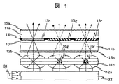
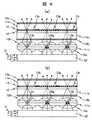
11b)と、その一対の基板で挟持された液晶層10と、一対の基板を挟持する一対の偏光板(第一の偏光板15a,第二の偏光板15b)と、カラーフィルタ(青のカラーフィルタ13b,緑のカラーフィルタ13g,赤のカラーフィルタ13r)と、ブラックマトリクス14とを有する構成とする。
11aと第二の基板11bと液晶層10からなり、第一の基板11aと第二の基板11bは液晶層10を挟持する。第一の基板11aと第二の基板11bは液晶層10に近接する面上に液晶層10の封入された液晶分子10′の配向状態を安定化するための一対の配向膜(第一の配向膜17a,第二の配向膜17b)を備える。また、第一の基板11aと第二の基板11bの一方もしくは両方に液晶層10に電圧を印加するための手段を備える。
17b,画素電極19,層間絶縁膜,共通電極18,走査配線,信号配線,アクティブ素子20、を備える。第二の配向膜17bは、第一の配向膜17aと同様にポリイミド系の有機高分子膜である。画素電極19と共通電極18はいずれも透明性と導電性を兼ね備えたインジウム錫酸化物(Indium Tin Oxide、ITO)であり、層厚は100nmである。両者は窒化珪素(SiN)製の層間絶縁膜によって隔たれており、層間絶縁膜の層厚は
500nmである。画素電極19の平面形状は櫛歯状であるのに対し、共通電極18は各画素の全面に渡って分布しており、電圧印加時に画素電極19と共通電極18の間にはアーチ状の電界が形成される。アーチ状の電界は液晶層10に平行な成分を有する所謂横電界であり、電界は近接する液晶層中にはみ出して分布することにより、液晶層10の液晶分子の配向状態を変形するIPS(In Plane Switching)方式液晶表示パネルである。
IPS方式液晶表示パネルでは電圧印加に伴う液晶層のチルト角増大が少ないため、視角方向での階調表示特性に優れた広視野角の表示が得られる。画素電極19と共通電極18が重畳する部分は液晶層10に対して並列に結合しているため、保持容量として機能する。
15bを配置し、一対の基板を挟持しており、第一の偏光板15aと第二の偏光板15bはヨウ素系色素を含み、その2色性で自然光を直線偏光に変換する。ヨウ素系色素の配向方向が吸収軸であり、第一の偏光板15aと第二の偏光板15bの吸収軸は互いに直交し、かつ第一の偏光板15aの吸収軸は液晶配向方向に平行である。
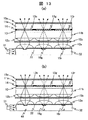
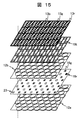
12bの平面分布をストライプ状にしたため、これに対応する第二のマイクロレンズアレイ12bの平面分布もストライプ状とした。
36と物体光37を作成し、両者を導光体32内部で交差させる。一般にレーザー光は径が小さいため、交差部をスキャンすれば導光体の全面に体積ホログラムを作成可能である。図6(b)に示した様に、光変換層に向かう出射光を再生光38,光源光を参照光36とみなすことが可能であり、この点において図6(a),(b)は一般的なホログラムの作成方法と同様である。
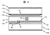
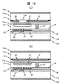
22に入射するように、蛍光体16の側面に蛍光体光反射層22を配置する。また、後方からは光源光が入射するが、これを妨げず、かつ後方に向かう蛍光成分がなるだけ多く蛍光体光反射層22に入射するように、後方にも部分的に蛍光体光反射層22を配置する。
26はジアクリル系液晶を光重合して形成する。位相差板26のリタデーションを310nmにし、段差形成層27で反射表示部の液晶層10のリタデーションを160nmにした。これに加えて、位相差板26の遅相軸が液晶配向方向となす角を67.5度 とすることにより、電圧無印加時に反射共通電極18′に入射する光の偏光状態を円偏光にでき、反射表示,透過表示ともノーマリクローズ表示にすることができる。
12(a)に示した様に、反射表示部の一部にカラーフィルタ13の存在しないカラーフィルタ開口部13hを配置することにより、反射表示部の面積平均した吸収率を低下している。しかし、カラーフィルタ開口部13hの面積が設計値から外れた場合に、反射表示のカラーバランスが崩れるなどの困難があった。
15bのみとなる。液晶表示装置全体を薄型化できるという長所を有する。
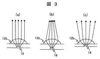
11bを介して存在する画素中心近傍に集光する。そのため、第二のマイクロレンズアレイ12bの焦点距離は第一のマイクロレンズアレイ12aに比較して著しく長いことが特徴である。
11(a)(b)と同様である。
12b上に光学部材を貼り付ける必要がなくなる。グリッドワイア偏光板は光の波長以下のピッチでスリットを形成した金属膜であり、スリットの垂直方向には金属膜の自由電子が動けないことから、スリット方向の直線偏光成分を反射し、スリット垂直方向の直線偏光成分を通過する性質を示す。
10′ 液晶分子
11a 第一の基板
11b 第二の基板
12a 第一のマイクロレンズアレイ
12b 第二のマイクロレンズアレイ
13 カラーフィルタ
13r 赤のカラーフィルタ
13g 緑のカラーフィルタ
13b 青のカラーフィルタ
13h カラーフィルタ開口部
13′ 反射表示用カラーフィルタ
14 ブラックマトリクス
15a 第一の偏光板
15b 第二の偏光板
16 蛍光体
16r 赤色の蛍光体
16g 緑色の蛍光体
17a 第一の配向膜
17b 第二の配向膜
18 共通電極
18′ 反射共通電極
19 画素電極
19t 透過部画素電極
20 アクティブ素子
21 コンタクトホール
22 蛍光体光反射層
23 光散乱層
24 平坦部吸収層
25 平坦部反射層
26 位相差板
27 段差形成層
31 光源
32 導光体
33 レーザー光源
34 ハーフミラー
35 ミラー
36 参照光
37 物体光
38 再生光
39 金属層
40a,40b 位置合わせマーク
48 ブレーズグレーティング
Claims (17)
- 第一の基板と、第二の基板と、前記第一の基板と第二の基板間に挟持された液晶層と、
を有して複数の画素を備える液晶パネルと、
青色光を出射する光源と、
前記液晶パネルと前記光源間に配置され、複数のレンズが配置された第一のマイクロレンズアレイと、複数のレンズが配置された第二のマイクロレンズアレイと、前記第一のマイクロレンズアレイと前記第二のマイクロレンズアレイ間に配置された蛍光体層と、を有する光変換層と、を有し、
前記光変換層の前記第一のマイクロレンズアレイは、前記光源からの青色光を前記蛍光体層に集光する機能を有し、
前記光変換層の前記第二のマイクロレンズアレイは、前記蛍光体層から出射された蛍光光、または前記光源からの青色光を、前記液晶パネル内の対応する画素に集光する機能を有し、
前記蛍光体層は、赤色蛍光体と、緑色蛍光体とを有し、
前記赤色蛍光体は、前記複数の画素のうち赤色表示を行う画素に対応して配置され、
前記緑色蛍光体は、前記複数の画素のうち緑色表示を行う画素に対応して配置された液晶表示装置。 - 請求項1記載の液晶表示装置において、
前記光源と前記光変換層間に配置され、前記光源からの青色光を前記光変換層へ出射する導光体を有する液晶表示装置。 - 請求項1記載の液晶表示装置において、
前記第一のマイクロレンズアレイの前記複数のレンズの断面形状は、前記光源が配置された側に対して凸形状であり、
前記第二のマイクロレンズアレイの前記複数のレンズの断面形状は、前記液晶パネルが配置された側に対して凸形状である液晶表示装置。 - 請求項1記載の液晶表示装置において、
前記液晶パネルは、カラーフィルタを有し、
前記赤色蛍光体と、前記緑色蛍光体は、前記複数の画素の各画素に位置する前記カラーフィルタの色に対応して配置された液晶表示装置。 - 請求項1記載の液晶表示装置において、
前記第一のマイクロレンズアレイと前記第二のマイクロレンズアレイは同一の平面分布を示す液晶表示装置。 - 請求項2記載の液晶表示装置において、
前記光源は、青色発光素子を有し、
前記青色発光素子は、前記導光体の一方側面に配置され、
前記導光体は、ホログラムまたはブレーズグレーティングが配置され、
前記ホログラムまたはブレーズグレーティングは、前記青色発光素子の発光を面状光源に変換して前記液晶パネルの法線方向に向かわせる液晶表示装置。 - 請求項1記載の液晶表示装置において、
前記蛍光体層は、前記第一のマイクロレンズアレイの焦点位置に配置された液晶表示装置。 - 請求項1記載の液晶表示装置において、
前記蛍光体層は、前記第二のマイクロレンズアレイの焦点位置よりも前記第二のマイクロレンズアレイから離れた位置に配置された液晶表示装置。 - 請求項1記載の液晶表示装置において、
前記第一のマイクロレンズアレイ及び前記第二のマイクロレンズアレイの前記複数のレンズのレンズ間に平坦部を有し、前記第一のマイクロレンズアレイと前記第二のマイクロレンズアレイ間に配置され、前記平坦部に対応する位置に平坦部吸収層若しくは平坦部反射層を配置した液晶表示装置。 - 請求項1記載の液晶表示装置において、
前記光変換層と前記液晶パネルの位置合わせのためのマークを、前記光変換層上及び前記液晶パネル上に形成した液晶表示装置。 - 請求項1記載の液晶表示装置において、
前記光変換層は、第三の基板を有し、
前記第一のマイクロレンズアレイと前記第二のマイクロレンズアレイは、前記第三の基板の異なる側に互いに形成され、前記蛍光体層は、前記第三の基板上に形成された液晶表示装置。 - 請求項1記載の液晶表示装置において、
前記液晶パネルが備える前記画素は、櫛歯状またはスリット状の画素電極と、前記画素全面にわたって形成されたべた状の共通電極を有する液晶表示装置。 - 請求項1記載の液晶表示装置において、
前記液晶パネルが備える前記複数の各画素は、透過表示部と反射表示部を有する液晶表示装置。 - 第一の基板と、第二の基板と、前記第一の基板と第二の基板間に挟持された液晶層と、を有して複数の画素を備える液晶パネルと、
前記液晶パネルを挟持する一対の偏光板と、
青色光を出射する光源と、
前記液晶パネルと前記光源間に配置された導光体と、
前記液晶パネルと前記導光体間に配置され、複数のレンズが配置された第一のマイクロレンズアレイと、複数のレンズが配置された第二のマイクロレンズアレイと、前記第一のマイクロレンズアレイと前記導光体間に配置された蛍光体層と、を有する光変換層と、
前記導光体と前記蛍光体層間に部分的に配置される蛍光体光反射層と、を有し、
前記一対の偏光板の一方の偏光板は、前記第一のマイクロレンズアレイと前記第二のマイクロレンズアレイ間に配置され、
前記蛍光体層は、赤色蛍光体と、緑色蛍光体とを有し、
前記赤色蛍光体は、前記複数の画素のうち赤色表示を行う画素に対応して配置され、
前記緑色蛍光体は、前記複数の画素のうち緑色表示を行う画素に対応して配置され、
前記光変換層の前記第一のマイクロレンズアレイは、前記赤色蛍光体および前記緑色蛍光体からの蛍光、または前記光源からの青色光を、平行光とする機能を有し、
前記光変換層の前記第二のマイクロレンズアレイは、前記赤色蛍光体および前記緑色蛍光体から前記一方の偏光板を介して出射された蛍光光、または前記光源から前記一方の偏光板を介して出射された青色光を、前記液晶パネル内の対応する画素に集光する機能を有する液晶表示装置。 - 請求項14記載の液晶表示装置において、
前記第一のマイクロレンズアレイの前記複数のレンズの断面形状は、前記液晶パネルが配置された側に対して凸形状であり、
前記第二のマイクロレンズアレイの前記複数のレンズの断面形状は、前記光源が配置された側に対して凸形状である液晶表示装置。 - 請求項14記載の液晶表示装置において、
前記導光体は、ブレーズグレーティングを有する液晶表示装置。 - 請求項14記載の液晶表示装置において、
前記液晶パネルが備える前記画素は、櫛歯状またはスリット状の画素電極と、前記画素全面にわたって形成されたべた状の共通電極を有する液晶表示装置。
Priority Applications (2)
| Application Number | Priority Date | Filing Date | Title |
|---|---|---|---|
| JP2006275964A JP4851908B2 (ja) | 2006-10-10 | 2006-10-10 | 液晶表示装置 |
| US11/869,900 US7639320B2 (en) | 2006-10-10 | 2007-10-10 | Liquid crystal display device |
Applications Claiming Priority (1)
| Application Number | Priority Date | Filing Date | Title |
|---|---|---|---|
| JP2006275964A JP4851908B2 (ja) | 2006-10-10 | 2006-10-10 | 液晶表示装置 |
Publications (2)
| Publication Number | Publication Date |
|---|---|
| JP2008096547A JP2008096547A (ja) | 2008-04-24 |
| JP4851908B2 true JP4851908B2 (ja) | 2012-01-11 |
Family
ID=39274690
Family Applications (1)
| Application Number | Title | Priority Date | Filing Date |
|---|---|---|---|
| JP2006275964A Expired - Fee Related JP4851908B2 (ja) | 2006-10-10 | 2006-10-10 | 液晶表示装置 |
Country Status (2)
| Country | Link |
|---|---|
| US (1) | US7639320B2 (ja) |
| JP (1) | JP4851908B2 (ja) |
Families Citing this family (36)
| Publication number | Priority date | Publication date | Assignee | Title |
|---|---|---|---|---|
| US20090218582A1 (en) * | 2008-02-28 | 2009-09-03 | Kang Wei-Hung | Optical device and method of fabricating the same |
| CN201174014Y (zh) * | 2008-04-10 | 2008-12-31 | 北京京东方光电科技有限公司 | 背光模组 |
| WO2010014057A1 (en) * | 2008-07-29 | 2010-02-04 | Thomson Licensing | Display characterization with filtration |
| JP4848404B2 (ja) * | 2008-09-04 | 2011-12-28 | 株式会社 日立ディスプレイズ | 液晶表示素子、および液晶表示装置 |
| US20100214282A1 (en) | 2009-02-24 | 2010-08-26 | Dolby Laboratories Licensing Corporation | Apparatus for providing light source modulation in dual modulator displays |
| JPWO2010116559A1 (ja) * | 2009-03-30 | 2012-10-18 | シャープ株式会社 | 表示パネルおよび表示装置 |
| US20110216266A1 (en) * | 2010-03-02 | 2011-09-08 | Microsoft Corporation | Wedge backlight with diffraction grating |
| JP5607430B2 (ja) * | 2010-06-10 | 2014-10-15 | 株式会社ジャパンディスプレイ | 立体映像表示装置及び電子機器 |
| US20120120467A1 (en) * | 2010-11-17 | 2012-05-17 | Qualcomm Mems Technologies, Inc. | Hybrid light guide with faceted and holographic light turning features |
| US8514352B2 (en) * | 2010-12-10 | 2013-08-20 | Sharp Kabushiki Kaisha | Phosphor-based display |
| US9564078B2 (en) | 2010-12-17 | 2017-02-07 | Dolby Laboratories Licensing Corporation | Quantum dots for display panels |
| KR101851726B1 (ko) | 2011-11-23 | 2018-04-24 | 엘지이노텍 주식회사 | 표시장치 |
| KR101360643B1 (ko) | 2012-05-09 | 2014-02-10 | 엘지이노텍 주식회사 | 광 변환 부재, 이를 포함하는 발광장치 및 표시장치 |
| KR102118309B1 (ko) | 2012-09-19 | 2020-06-03 | 돌비 레버러토리즈 라이쎈싱 코오포레이션 | 양자점/리모트 인광 디스플레이 시스템 개선 |
| JP6340554B2 (ja) * | 2012-12-26 | 2018-06-13 | パナソニックIpマネジメント株式会社 | 画像表示装置 |
| US9436056B2 (en) * | 2013-02-06 | 2016-09-06 | E Ink Corporation | Color electro-optic displays |
| EP2965308B1 (en) | 2013-03-08 | 2020-09-09 | Dolby Laboratories Licensing Corporation | Techniques for dual modulation display with light conversion |
| JP6087872B2 (ja) * | 2013-08-12 | 2017-03-01 | 富士フイルム株式会社 | 光学フィルム、バリアフィルム、光変換部材、バックライトユニットおよび液晶表示装置 |
| CN111243533B (zh) | 2014-03-26 | 2022-11-25 | 杜比实验室特许公司 | 各种显示器中的全局光补偿 |
| CN108873477B (zh) * | 2014-08-21 | 2021-08-17 | 杜比实验室特许公司 | 用于驱动局部调光显示器的方法、设备和存储介质 |
| US20160093269A1 (en) * | 2014-09-26 | 2016-03-31 | Pixtronix, Inc. | Laser-Pumped Phosphor Backlight and Methods |
| US9470925B2 (en) * | 2014-09-30 | 2016-10-18 | Shenzhen China Star Optoelectronics Technology Co., Ltd | Liquid crystal display device |
| KR101621820B1 (ko) | 2014-12-29 | 2016-05-17 | 삼성전자 주식회사 | 광원, 광원을 포함하는 백라이트 유닛 및 액정 표시 장치 |
| CN105929591B (zh) | 2016-07-08 | 2019-04-05 | 京东方科技集团股份有限公司 | 量子点显示基板及其制造方法和量子点显示装置 |
| KR102712901B1 (ko) | 2016-08-17 | 2024-10-07 | 삼성전자주식회사 | 디스플레이 패널 및 이를 포함하는 디스플레이 장치 |
| CN107402473B (zh) * | 2017-09-25 | 2020-11-06 | 京东方科技集团股份有限公司 | 显示模组和显示装置 |
| CN108051945B (zh) * | 2018-01-02 | 2021-03-16 | 京东方科技集团股份有限公司 | 一种显示组件、液晶显示器和电子设备 |
| CN108415191A (zh) * | 2018-03-15 | 2018-08-17 | 京东方科技集团股份有限公司 | 显示装置、电子设备和显示方法 |
| CN109100871B (zh) * | 2018-09-14 | 2021-09-03 | 京东方科技集团股份有限公司 | 光调制装置以及光谱检测系统 |
| EP3671711A1 (en) * | 2018-12-20 | 2020-06-24 | IMEC vzw | Cross-talk reduction in display with optical scanner |
| CN110646982B (zh) * | 2019-10-08 | 2021-08-10 | 京东方科技集团股份有限公司 | 液晶显示面板及其驱动方法、显示装置 |
| CN111175982B (zh) * | 2020-02-24 | 2023-01-17 | 京东方科技集团股份有限公司 | 近眼显示装置和可穿戴设备 |
| CN113534456A (zh) * | 2020-04-22 | 2021-10-22 | 京东方科技集团股份有限公司 | 一种近眼显示设备和近眼显示装置 |
| CN112054131B (zh) * | 2020-09-14 | 2022-09-20 | 京东方科技集团股份有限公司 | 显示面板、显示装置及显示设备 |
| CN112859347A (zh) * | 2021-02-25 | 2021-05-28 | 京东方科技集团股份有限公司 | 近眼显示装置及可穿戴设备 |
| CN117031814A (zh) * | 2023-07-03 | 2023-11-10 | 联想(北京)有限公司 | 显示装置、处理方法及处理器 |
Family Cites Families (10)
| Publication number | Priority date | Publication date | Assignee | Title |
|---|---|---|---|---|
| US4798448A (en) * | 1988-02-16 | 1989-01-17 | General Electric Company | High efficiency illumination system for display devices |
| JP3528994B2 (ja) * | 1994-11-08 | 2004-05-24 | 大日本印刷株式会社 | 液晶表示装置用平行光源及びそれを用いた液晶表示装置 |
| JP3405087B2 (ja) * | 1995-11-06 | 2003-05-12 | ソニー株式会社 | 液晶表示装置およびその製造方法 |
| JPH09167513A (ja) * | 1995-12-15 | 1997-06-24 | Kuraray Co Ltd | 面光源素子 |
| JP2865618B2 (ja) * | 1996-05-31 | 1999-03-08 | 嶋田プレシジョン株式会社 | 導光板および導光板アセンブリ |
| JP2001133770A (ja) * | 1999-11-04 | 2001-05-18 | Hitachi Ltd | 液晶表示装置 |
| JP2003015122A (ja) | 2001-06-27 | 2003-01-15 | Seiko Epson Corp | 液晶表示装置および電子機器 |
| JP2003015121A (ja) | 2001-06-27 | 2003-01-15 | Seiko Epson Corp | 液晶表示装置および電子機器 |
| JP2005353650A (ja) | 2004-06-08 | 2005-12-22 | Matsushita Electric Ind Co Ltd | Led光源および液晶表示装置 |
| JP2006012722A (ja) * | 2004-06-29 | 2006-01-12 | Sharp Corp | バックライト装置、およびそれを備えた液晶表示装置 |
-
2006
- 2006-10-10 JP JP2006275964A patent/JP4851908B2/ja not_active Expired - Fee Related
-
2007
- 2007-10-10 US US11/869,900 patent/US7639320B2/en not_active Expired - Fee Related
Also Published As
| Publication number | Publication date |
|---|---|
| JP2008096547A (ja) | 2008-04-24 |
| US7639320B2 (en) | 2009-12-29 |
| US20080084517A1 (en) | 2008-04-10 |
Similar Documents
| Publication | Publication Date | Title |
|---|---|---|
| JP4851908B2 (ja) | 液晶表示装置 | |
| JP5112230B2 (ja) | 液晶表示装置 | |
| US8345182B2 (en) | Liquid crystal display device | |
| KR101222566B1 (ko) | 디스플레이패널 및 이를 포함하는 디스플레이장치 | |
| JP4778873B2 (ja) | 液晶表示装置 | |
| US6469755B1 (en) | Illuminating arrangement with reflector having inclined irregularities or corrugations | |
| JP3957986B2 (ja) | 反射型表示装置 | |
| JPH10325953A (ja) | 反射型兼透過型表示装置 | |
| CN102681164B (zh) | 调光装置及显示器 | |
| JP3506978B2 (ja) | 反射型液晶表示装置 | |
| US10558083B2 (en) | Liquid crystal display module and liquid crystal display device | |
| JP2013235141A (ja) | カラー液晶表示装置 | |
| CN111025728A (zh) | 显示装置 | |
| JP2015225114A (ja) | 表示装置及び液晶表示装置 | |
| US20180196302A1 (en) | Display device | |
| JP2003195275A (ja) | 液晶表示装置 | |
| US8531629B2 (en) | Reflective display device including polymer-dispersed liquid crystals having particular light-absorbing member | |
| JP4436752B2 (ja) | 光源装置および液晶表示装置 | |
| TW202430990A (zh) | 光學元件及其製造方法以及照明裝置 | |
| JP4112663B2 (ja) | 液晶表示装置 | |
| JP2009092972A (ja) | 表示装置 | |
| JPH0815689A (ja) | 液晶表示器 | |
| KR101213104B1 (ko) | 마이크로렌즈 어레이 시트 및 이를 이용한 액정 표시 장치 | |
| JP2001133777A (ja) | 液晶表示装置 | |
| JP2004013059A (ja) | 液晶表示装置および電子機器 |
Legal Events
| Date | Code | Title | Description |
|---|---|---|---|
| A621 | Written request for application examination |
Free format text: JAPANESE INTERMEDIATE CODE: A621 Effective date: 20090225 |
|
| A521 | Written amendment |
Free format text: JAPANESE INTERMEDIATE CODE: A523 Effective date: 20090225 |
|
| RD02 | Notification of acceptance of power of attorney |
Free format text: JAPANESE INTERMEDIATE CODE: A7422 Effective date: 20100127 |
|
| RD04 | Notification of resignation of power of attorney |
Free format text: JAPANESE INTERMEDIATE CODE: A7424 Effective date: 20100301 |
|
| A711 | Notification of change in applicant |
Free format text: JAPANESE INTERMEDIATE CODE: A712 Effective date: 20110112 |
|
| A977 | Report on retrieval |
Free format text: JAPANESE INTERMEDIATE CODE: A971007 Effective date: 20110622 |
|
| A131 | Notification of reasons for refusal |
Free format text: JAPANESE INTERMEDIATE CODE: A131 Effective date: 20110705 |
|
| A521 | Written amendment |
Free format text: JAPANESE INTERMEDIATE CODE: A523 Effective date: 20110905 |
|
| TRDD | Decision of grant or rejection written | ||
| A01 | Written decision to grant a patent or to grant a registration (utility model) |
Free format text: JAPANESE INTERMEDIATE CODE: A01 Effective date: 20110927 |
|
| A01 | Written decision to grant a patent or to grant a registration (utility model) |
Free format text: JAPANESE INTERMEDIATE CODE: A01 |
|
| A61 | First payment of annual fees (during grant procedure) |
Free format text: JAPANESE INTERMEDIATE CODE: A61 Effective date: 20111021 |
|
| R150 | Certificate of patent or registration of utility model |
Ref document number: 4851908 Country of ref document: JP Free format text: JAPANESE INTERMEDIATE CODE: R150 Free format text: JAPANESE INTERMEDIATE CODE: R150 |
|
| FPAY | Renewal fee payment (event date is renewal date of database) |
Free format text: PAYMENT UNTIL: 20141028 Year of fee payment: 3 |
|
| R250 | Receipt of annual fees |
Free format text: JAPANESE INTERMEDIATE CODE: R250 |
|
| R250 | Receipt of annual fees |
Free format text: JAPANESE INTERMEDIATE CODE: R250 |
|
| R250 | Receipt of annual fees |
Free format text: JAPANESE INTERMEDIATE CODE: R250 |
|
| R250 | Receipt of annual fees |
Free format text: JAPANESE INTERMEDIATE CODE: R250 |
|
| R250 | Receipt of annual fees |
Free format text: JAPANESE INTERMEDIATE CODE: R250 |
|
| R250 | Receipt of annual fees |
Free format text: JAPANESE INTERMEDIATE CODE: R250 |
|
| LAPS | Cancellation because of no payment of annual fees |