JP4851908B2 - Liquid crystal display - Google Patents
Liquid crystal display Download PDFInfo
- Publication number
- JP4851908B2 JP4851908B2 JP2006275964A JP2006275964A JP4851908B2 JP 4851908 B2 JP4851908 B2 JP 4851908B2 JP 2006275964 A JP2006275964 A JP 2006275964A JP 2006275964 A JP2006275964 A JP 2006275964A JP 4851908 B2 JP4851908 B2 JP 4851908B2
- Authority
- JP
- Japan
- Prior art keywords
- liquid crystal
- light
- microlens array
- crystal display
- display device
- Prior art date
- Legal status (The legal status is an assumption and is not a legal conclusion. Google has not performed a legal analysis and makes no representation as to the accuracy of the status listed.)
- Expired - Fee Related
Links
- 239000004973 liquid crystal related substance Substances 0.000 title claims description 153
- OAICVXFJPJFONN-UHFFFAOYSA-N Phosphorus Chemical compound [P] OAICVXFJPJFONN-UHFFFAOYSA-N 0.000 claims description 117
- 239000000758 substrate Substances 0.000 claims description 83
- 238000006243 chemical reaction Methods 0.000 claims description 41
- 238000009826 distribution Methods 0.000 claims description 9
- 239000007787 solid Substances 0.000 claims description 3
- 239000010410 layer Substances 0.000 description 139
- 239000010408 film Substances 0.000 description 23
- 238000000034 method Methods 0.000 description 15
- 230000003287 optical effect Effects 0.000 description 13
- 230000008859 change Effects 0.000 description 11
- 230000005684 electric field Effects 0.000 description 11
- 238000000149 argon plasma sintering Methods 0.000 description 10
- 239000011159 matrix material Substances 0.000 description 10
- 238000010521 absorption reaction Methods 0.000 description 8
- 230000000694 effects Effects 0.000 description 8
- 229910052751 metal Inorganic materials 0.000 description 6
- 239000002184 metal Substances 0.000 description 6
- 230000009471 action Effects 0.000 description 5
- 230000007423 decrease Effects 0.000 description 5
- 239000000975 dye Substances 0.000 description 5
- 230000008569 process Effects 0.000 description 5
- 230000009467 reduction Effects 0.000 description 5
- 239000011347 resin Substances 0.000 description 5
- 229920005989 resin Polymers 0.000 description 5
- 239000010419 fine particle Substances 0.000 description 4
- 230000005499 meniscus Effects 0.000 description 4
- 238000000206 photolithography Methods 0.000 description 4
- 239000000126 substance Substances 0.000 description 4
- 230000008901 benefit Effects 0.000 description 3
- 230000005540 biological transmission Effects 0.000 description 3
- 230000006872 improvement Effects 0.000 description 3
- 239000011229 interlayer Substances 0.000 description 3
- ZCYVEMRRCGMTRW-UHFFFAOYSA-N 7553-56-2 Chemical compound [I] ZCYVEMRRCGMTRW-UHFFFAOYSA-N 0.000 description 2
- 239000004642 Polyimide Substances 0.000 description 2
- 229910052581 Si3N4 Inorganic materials 0.000 description 2
- 229910052782 aluminium Inorganic materials 0.000 description 2
- XAGFODPZIPBFFR-UHFFFAOYSA-N aluminium Chemical compound [Al] XAGFODPZIPBFFR-UHFFFAOYSA-N 0.000 description 2
- 239000005388 borosilicate glass Substances 0.000 description 2
- 238000005229 chemical vapour deposition Methods 0.000 description 2
- 230000001427 coherent effect Effects 0.000 description 2
- 239000003086 colorant Substances 0.000 description 2
- ZYGHJZDHTFUPRJ-UHFFFAOYSA-N coumarin Chemical compound C1=CC=C2OC(=O)C=CC2=C1 ZYGHJZDHTFUPRJ-UHFFFAOYSA-N 0.000 description 2
- 238000013461 design Methods 0.000 description 2
- 229910052740 iodine Inorganic materials 0.000 description 2
- 239000011630 iodine Substances 0.000 description 2
- 230000031700 light absorption Effects 0.000 description 2
- 239000012788 optical film Substances 0.000 description 2
- 229920000620 organic polymer Polymers 0.000 description 2
- 230000010287 polarization Effects 0.000 description 2
- 229910021420 polycrystalline silicon Inorganic materials 0.000 description 2
- 229920001721 polyimide Polymers 0.000 description 2
- 229920005591 polysilicon Polymers 0.000 description 2
- 238000012545 processing Methods 0.000 description 2
- HQVNEWCFYHHQES-UHFFFAOYSA-N silicon nitride Chemical compound N12[Si]34N5[Si]62N3[Si]51N64 HQVNEWCFYHHQES-UHFFFAOYSA-N 0.000 description 2
- 238000004611 spectroscopical analysis Methods 0.000 description 2
- BCHZICNRHXRCHY-UHFFFAOYSA-N 2h-oxazine Chemical compound N1OC=CC=C1 BCHZICNRHXRCHY-UHFFFAOYSA-N 0.000 description 1
- CZPWVGJYEJSRLH-UHFFFAOYSA-N Pyrimidine Chemical compound C1=CN=CN=C1 CZPWVGJYEJSRLH-UHFFFAOYSA-N 0.000 description 1
- 239000000853 adhesive Substances 0.000 description 1
- 230000001070 adhesive effect Effects 0.000 description 1
- 229910021417 amorphous silicon Inorganic materials 0.000 description 1
- 238000003491 array Methods 0.000 description 1
- XJHABGPPCLHLLV-UHFFFAOYSA-N benzo[de]isoquinoline-1,3-dione Chemical compound C1=CC(C(=O)NC2=O)=C3C2=CC=CC3=C1 XJHABGPPCLHLLV-UHFFFAOYSA-N 0.000 description 1
- 230000015572 biosynthetic process Effects 0.000 description 1
- 239000003990 capacitor Substances 0.000 description 1
- 238000004891 communication Methods 0.000 description 1
- 239000012141 concentrate Substances 0.000 description 1
- 229960000956 coumarin Drugs 0.000 description 1
- 235000001671 coumarin Nutrition 0.000 description 1
- 230000003247 decreasing effect Effects 0.000 description 1
- 230000002999 depolarising effect Effects 0.000 description 1
- 125000004386 diacrylate group Chemical group 0.000 description 1
- 238000010586 diagram Methods 0.000 description 1
- 238000009792 diffusion process Methods 0.000 description 1
- 239000006185 dispersion Substances 0.000 description 1
- 239000003574 free electron Substances 0.000 description 1
- 238000010438 heat treatment Methods 0.000 description 1
- 239000012535 impurity Substances 0.000 description 1
- AMGQUBHHOARCQH-UHFFFAOYSA-N indium;oxotin Chemical compound [In].[Sn]=O AMGQUBHHOARCQH-UHFFFAOYSA-N 0.000 description 1
- 238000004519 manufacturing process Methods 0.000 description 1
- 239000000463 material Substances 0.000 description 1
- 230000004048 modification Effects 0.000 description 1
- 238000012986 modification Methods 0.000 description 1
- 238000000059 patterning Methods 0.000 description 1
- 230000000737 periodic effect Effects 0.000 description 1
- 239000000049 pigment Substances 0.000 description 1
- 238000002360 preparation method Methods 0.000 description 1
- 239000001022 rhodamine dye Substances 0.000 description 1
- 230000007480 spreading Effects 0.000 description 1
- 238000003892 spreading Methods 0.000 description 1
- 230000000087 stabilizing effect Effects 0.000 description 1
- 238000003860 storage Methods 0.000 description 1
- 239000010409 thin film Substances 0.000 description 1
- 229910052725 zinc Inorganic materials 0.000 description 1
Images


Classifications
-
- G—PHYSICS
- G02—OPTICS
- G02F—OPTICAL DEVICES OR ARRANGEMENTS FOR THE CONTROL OF LIGHT BY MODIFICATION OF THE OPTICAL PROPERTIES OF THE MEDIA OF THE ELEMENTS INVOLVED THEREIN; NON-LINEAR OPTICS; FREQUENCY-CHANGING OF LIGHT; OPTICAL LOGIC ELEMENTS; OPTICAL ANALOGUE/DIGITAL CONVERTERS
- G02F1/00—Devices or arrangements for the control of the intensity, colour, phase, polarisation or direction of light arriving from an independent light source, e.g. switching, gating or modulating; Non-linear optics
- G02F1/01—Devices or arrangements for the control of the intensity, colour, phase, polarisation or direction of light arriving from an independent light source, e.g. switching, gating or modulating; Non-linear optics for the control of the intensity, phase, polarisation or colour
- G02F1/13—Devices or arrangements for the control of the intensity, colour, phase, polarisation or direction of light arriving from an independent light source, e.g. switching, gating or modulating; Non-linear optics for the control of the intensity, phase, polarisation or colour based on liquid crystals, e.g. single liquid crystal display cells
- G02F1/133—Constructional arrangements; Operation of liquid crystal cells; Circuit arrangements
- G02F1/1333—Constructional arrangements; Manufacturing methods
- G02F1/1335—Structural association of cells with optical devices, e.g. polarisers or reflectors
- G02F1/133553—Reflecting elements
- G02F1/133555—Transflectors
-
- G—PHYSICS
- G02—OPTICS
- G02F—OPTICAL DEVICES OR ARRANGEMENTS FOR THE CONTROL OF LIGHT BY MODIFICATION OF THE OPTICAL PROPERTIES OF THE MEDIA OF THE ELEMENTS INVOLVED THEREIN; NON-LINEAR OPTICS; FREQUENCY-CHANGING OF LIGHT; OPTICAL LOGIC ELEMENTS; OPTICAL ANALOGUE/DIGITAL CONVERTERS
- G02F1/00—Devices or arrangements for the control of the intensity, colour, phase, polarisation or direction of light arriving from an independent light source, e.g. switching, gating or modulating; Non-linear optics
- G02F1/01—Devices or arrangements for the control of the intensity, colour, phase, polarisation or direction of light arriving from an independent light source, e.g. switching, gating or modulating; Non-linear optics for the control of the intensity, phase, polarisation or colour
- G02F1/13—Devices or arrangements for the control of the intensity, colour, phase, polarisation or direction of light arriving from an independent light source, e.g. switching, gating or modulating; Non-linear optics for the control of the intensity, phase, polarisation or colour based on liquid crystals, e.g. single liquid crystal display cells
- G02F1/133—Constructional arrangements; Operation of liquid crystal cells; Circuit arrangements
- G02F1/1333—Constructional arrangements; Manufacturing methods
- G02F1/1335—Structural association of cells with optical devices, e.g. polarisers or reflectors
- G02F1/133509—Filters, e.g. light shielding masks
- G02F1/133514—Colour filters
-
- G—PHYSICS
- G02—OPTICS
- G02F—OPTICAL DEVICES OR ARRANGEMENTS FOR THE CONTROL OF LIGHT BY MODIFICATION OF THE OPTICAL PROPERTIES OF THE MEDIA OF THE ELEMENTS INVOLVED THEREIN; NON-LINEAR OPTICS; FREQUENCY-CHANGING OF LIGHT; OPTICAL LOGIC ELEMENTS; OPTICAL ANALOGUE/DIGITAL CONVERTERS
- G02F1/00—Devices or arrangements for the control of the intensity, colour, phase, polarisation or direction of light arriving from an independent light source, e.g. switching, gating or modulating; Non-linear optics
- G02F1/01—Devices or arrangements for the control of the intensity, colour, phase, polarisation or direction of light arriving from an independent light source, e.g. switching, gating or modulating; Non-linear optics for the control of the intensity, phase, polarisation or colour
- G02F1/13—Devices or arrangements for the control of the intensity, colour, phase, polarisation or direction of light arriving from an independent light source, e.g. switching, gating or modulating; Non-linear optics for the control of the intensity, phase, polarisation or colour based on liquid crystals, e.g. single liquid crystal display cells
- G02F1/133—Constructional arrangements; Operation of liquid crystal cells; Circuit arrangements
- G02F1/1333—Constructional arrangements; Manufacturing methods
- G02F1/1335—Structural association of cells with optical devices, e.g. polarisers or reflectors
- G02F1/1336—Illuminating devices
- G02F1/133621—Illuminating devices providing coloured light
-
- G—PHYSICS
- G02—OPTICS
- G02B—OPTICAL ELEMENTS, SYSTEMS OR APPARATUS
- G02B6/00—Light guides; Structural details of arrangements comprising light guides and other optical elements, e.g. couplings
- G02B6/0001—Light guides; Structural details of arrangements comprising light guides and other optical elements, e.g. couplings specially adapted for lighting devices or systems
- G02B6/0011—Light guides; Structural details of arrangements comprising light guides and other optical elements, e.g. couplings specially adapted for lighting devices or systems the light guides being planar or of plate-like form
- G02B6/0033—Means for improving the coupling-out of light from the light guide
- G02B6/0035—Means for improving the coupling-out of light from the light guide provided on the surface of the light guide or in the bulk of it
- G02B6/0038—Linear indentations or grooves, e.g. arc-shaped grooves or meandering grooves, extending over the full length or width of the light guide
-
- G—PHYSICS
- G02—OPTICS
- G02F—OPTICAL DEVICES OR ARRANGEMENTS FOR THE CONTROL OF LIGHT BY MODIFICATION OF THE OPTICAL PROPERTIES OF THE MEDIA OF THE ELEMENTS INVOLVED THEREIN; NON-LINEAR OPTICS; FREQUENCY-CHANGING OF LIGHT; OPTICAL LOGIC ELEMENTS; OPTICAL ANALOGUE/DIGITAL CONVERTERS
- G02F1/00—Devices or arrangements for the control of the intensity, colour, phase, polarisation or direction of light arriving from an independent light source, e.g. switching, gating or modulating; Non-linear optics
- G02F1/01—Devices or arrangements for the control of the intensity, colour, phase, polarisation or direction of light arriving from an independent light source, e.g. switching, gating or modulating; Non-linear optics for the control of the intensity, phase, polarisation or colour
- G02F1/13—Devices or arrangements for the control of the intensity, colour, phase, polarisation or direction of light arriving from an independent light source, e.g. switching, gating or modulating; Non-linear optics for the control of the intensity, phase, polarisation or colour based on liquid crystals, e.g. single liquid crystal display cells
- G02F1/133—Constructional arrangements; Operation of liquid crystal cells; Circuit arrangements
- G02F1/1333—Constructional arrangements; Manufacturing methods
- G02F1/1335—Structural association of cells with optical devices, e.g. polarisers or reflectors
- G02F1/1336—Illuminating devices
- G02F1/133614—Illuminating devices using photoluminescence, e.g. phosphors illuminated by UV or blue light
Landscapes
- Physics & Mathematics (AREA)
- Nonlinear Science (AREA)
- Mathematical Physics (AREA)
- Chemical & Material Sciences (AREA)
- Crystallography & Structural Chemistry (AREA)
- General Physics & Mathematics (AREA)
- Optics & Photonics (AREA)
- Liquid Crystal (AREA)
Description
本発明は表示効率の良い液晶表示装置に関する。 The present invention relates to a liquid crystal display device with high display efficiency.
携帯電話に代表される携帯型情報機器は通信速度を高速化しながら多機能化,高機能化していくことが予想され、大容量の画像情報に対応する必要があることから、高画質であること、高精細表示が可能であることが要求される。高画質に関してより具体的には、高コントラスト,高色再現性,広視野角,屋外視認性が挙げられる。また、限られた重量と容積に多種のデバイスを組み込むことから、薄型,軽量,低消費電力も要求される。 Mobile information devices such as mobile phones are expected to be multi-functional and highly functional at high communication speeds, and must support high-capacity image information. High-definition display is required. More specifically, high contrast, high contrast, high color reproducibility, wide viewing angle, and outdoor visibility. In addition, since various devices are incorporated in a limited weight and volume, thin, lightweight, and low power consumption are also required.
携帯型情報機器は多様な環境下で用いられるが、明るい環境の極限として真夏の直射日光下が、暗い環境の極限として暗室が挙げられる。これら多様な環境の全般において比較的良好な表示を得るために、1画素内に透過領域と反射領域を有する半透過型液晶表示装置が用いられることが多い。 Portable information devices are used in a variety of environments, including the midsummer direct sunlight as the limit of bright environments and the dark room as the limit of dark environments. In order to obtain a relatively good display in all of these various environments, a transflective liquid crystal display device having a transmissive region and a reflective region in one pixel is often used.
液晶表示装置の光源には白色発光ダイオードが用いられており、これは青色発光ダイオードの発光を黄色発光の蛍光体に通し、両者の発光の混色により白色としたものである。また、液晶表示装置の液晶パネル内部には光吸収性のカラーフィルタを備え、光シャッターである液晶表示装置と組み合わせてカラー表示を行う。 A white light emitting diode is used as a light source of the liquid crystal display device, and the light emitted from the blue light emitting diode is passed through a phosphor emitting yellow light and is made white by mixing the light emitted from both. In addition, a light-absorbing color filter is provided inside the liquid crystal panel of the liquid crystal display device, and color display is performed in combination with a liquid crystal display device that is an optical shutter.
また液晶表示装置には光吸収性の部材が用いられており、液晶表示装置の表示効率低下の要因になっている。光吸収性の部材のなかでも偏光板とカラーフィルタの光吸収率がとりわけ高いが、いずれも液晶表示装置の表示原理の根幹を成すものである。 In addition, a light-absorbing member is used in the liquid crystal display device, which causes a reduction in display efficiency of the liquid crystal display device. Among the light-absorbing members, the polarizing plate and the color filter have particularly high light absorptivity, but both form the basis of the display principle of the liquid crystal display device.
液晶表示装置の表示効率を向上するため、各種の光学素子が考案されている。先ほどの半透過液晶表示装置との関連では、マイクロレンズの使用が考えられている。即ち、半透過液晶では一画素中の面積分割された一部分が透過表示部であり、主に反射表示部からなる他の部分に入射した光は大部分が利用されない。マイクロレンズを用いて光源光を透過表示部に集光すれば、原理上は光源光の大部分を有効利用できるはずである。 In order to improve the display efficiency of the liquid crystal display device, various optical elements have been devised. In connection with the above-described transflective liquid crystal display device, use of a microlens is considered. That is, in the transflective liquid crystal, a part of one pixel whose area is divided is a transmissive display part, and most of the light incident on the other part mainly composed of the reflective display part is not used. If light source light is condensed on a transmissive display unit using a microlens, in principle, most of the light source light should be able to be used effectively.
あるいはまた、蛍光体による色変換の使用が考えられている。即ち、光源光を紫外光もしくは青色光にし、蛍光体を用いて赤色光,緑色光,青色光に変換する。その後に対応するカラーフィルタに入射すれば、原理上はカラーフィルタによる光吸収を低減できるはずである。蛍光体のほかにも、例えばホログラムを用いて白色光源を赤色光,緑色光,青色光に分光して、対応するカラーフィルタに入射しても原理上同様の効果が得られるはずである。 Alternatively, the use of color conversion with phosphors is considered. That is, the light source light is converted into ultraviolet light or blue light and converted into red light, green light, and blue light using a phosphor. If the light then enters a corresponding color filter, in principle, light absorption by the color filter should be reduced. In addition to the fluorescent material, for example, if a white light source is split into red light, green light, and blue light using a hologram and is incident on a corresponding color filter, the same effect should be obtained in principle.
マイクロレンズとホログラムを用いた液晶表示装置の表示効率向上は、例えば、特許文献1,特許文献2に記載されている。また、側面に配置された発光ダイオードの青色光を、蛍光体を用いて赤色光,緑色光,青色光に変換する効率向上については、特許文献3に記載されている。
Improvement of display efficiency of a liquid crystal display device using a microlens and a hologram is described in Patent Document 1 and
上記従来技術のようにマイクロレンズとホログラムを用いる場合、マイクロレンズは光源光のコリメート性が高くなければ十分な集光ができなく、且つホログラム,マイクロレンズ,液晶パネルの3者の位置合わせが必要であり、製造が困難である。また蛍光体を用いる場合、蛍光体は光源光を吸収して発光する過程で偏光を解消し、かつ光を散乱する性質を有する。これらの性質を考慮した上で、光源から液晶パネルまでを含む全体設計をしなければ、所望の表示効率向上の効果が得られない。 When a microlens and a hologram are used as in the above prior art, the microlens cannot be sufficiently condensed unless the light source light is highly collimated, and alignment between the hologram, microlens and liquid crystal panel is necessary. It is difficult to manufacture. When a phosphor is used, the phosphor has a property of depolarizing and scattering light in the process of absorbing and emitting light from the light source. Considering these properties, the desired display efficiency improvement effect cannot be obtained unless the overall design including the light source to the liquid crystal panel is made.
本発明の目的は、このような課題に鑑み、分光及び集光の最適な組み合わせによる高い表示効率の液晶表示装置を提供することである。 In view of such problems, an object of the present invention is to provide a liquid crystal display device with high display efficiency by an optimal combination of spectroscopy and light collection.
本発明では、上記目的を解決するために、第一の基板と、第二の基板と、第一の基板と第二の基板間に挟持された液晶層と、を有する液晶パネルと、青色光を出射する光源と、液晶パネルと光源間に配置され、複数のレンズが配置された第一のマイクロレンズアレイと、複数のレンズが配置された第二のマイクロレンズアレイと、第一のマイクロレンズアレイと第二のマイクロレンズアレイ間に配置された蛍光体層と、を有する光変換層と、を有する構成とする。 In the present invention, in order to solve the above object, a liquid crystal panel having a first substrate, a second substrate, a liquid crystal layer sandwiched between the first substrate and the second substrate, and blue light , A first microlens array in which a plurality of lenses are arranged, a second microlens array in which a plurality of lenses are arranged, and a first microlens A light conversion layer having a phosphor layer disposed between the array and the second microlens array is provided.
また、光変換層の第一のマイクロレンズアレイは、光源からの青色光を蛍光体層に集光する機能を有し、光変換層の第二のマイクロレンズアレイは、蛍光体層から出射された蛍光光、または光源からの青色光を、液晶パネル内の対応する画素に集光する機能を有する構成とする。 The first microlens array of the light conversion layer has a function of condensing blue light from the light source onto the phosphor layer, and the second microlens array of the light conversion layer is emitted from the phosphor layer. The fluorescent light or the blue light from the light source has a function of condensing on the corresponding pixel in the liquid crystal panel.
また、第一のマイクロレンズアレイの複数のレンズの断面形状は、光源が配置された側に対して凸形状であり、第二のマイクロレンズアレイの複数のレンズの断面形状は、液晶パネルが配置された側に対して凸形状である構成とする。 The cross-sectional shape of the plurality of lenses of the first microlens array is convex with respect to the side where the light source is disposed, and the cross-sectional shape of the plurality of lenses of the second microlens array is disposed by the liquid crystal panel. It is set as the structure which is convex shape with respect to the made side.
また、光源は、青色発光素子を有し、その青色発光素子は、導光体の一方側面に配置され、導光体は、ホログラムまたはブレーズグレーティングが配置され、ホログラムまたはブレーズグレーティングは、青色発光素子の発光を面状光源に変換して液晶パネルの法線方向に向かわせる構成とする。 The light source has a blue light emitting element, the blue light emitting element is disposed on one side surface of the light guide, the light guide is disposed with a hologram or a blazed grating, and the hologram or blazed grating is a blue light emitting element. The emitted light is converted into a planar light source and directed in the normal direction of the liquid crystal panel.
また、第一の基板と、第二の基板と、第一の基板と第二の基板間に挟持された液晶層と、を有する液晶パネルと、液晶パネルを挟持する一対の偏光板と、青色光を出射する光源と、液晶パネルと光源間に配置された導光体と、液晶パネルと導光体間に配置され、複数のレンズが配置された第一のマイクロレンズと、複数のレンズが配置された第二のマイクロレンズアレイと、第一のマイクロレンズアレイと導光体間に配置された蛍光体層と、を有する光変換層と、導光体と蛍光体層間に蛍光体光反射層と、を有し、一対の偏光板の一方の偏光板は、第一のマイクロレンズアレイと第二のマイクロレンズアレイ間に配置された構成とする。 A liquid crystal panel having a first substrate, a second substrate, a liquid crystal layer sandwiched between the first substrate and the second substrate, a pair of polarizing plates sandwiching the liquid crystal panel, and blue A light source that emits light, a light guide disposed between the liquid crystal panel and the light source, a first microlens disposed between the liquid crystal panel and the light guide, and a plurality of lenses disposed; A light conversion layer having a second microlens array disposed; a phosphor layer disposed between the first microlens array and the light guide; and phosphor light reflection between the light guide and the phosphor layer. And one polarizing plate of the pair of polarizing plates is arranged between the first microlens array and the second microlens array.
また、第一のマイクロレンズアレイの複数のレンズの断面形状は、液晶パネルが配置された側に対して凸形状であり、第二のマイクロレンズアレイの複数のレンズの断面形状は、光源が配置された側に対して凸形状である構成とする。 The cross-sectional shape of the plurality of lenses in the first microlens array is convex with respect to the side on which the liquid crystal panel is disposed, and the light source is disposed in the cross-sectional shape of the plurality of lenses in the second microlens array. It is set as the structure which is convex shape with respect to the made side.
本発明によれば、分光及び集光の最適な組み合わせによる高い表示効率の液晶表示装置が提供できる。 ADVANTAGE OF THE INVENTION According to this invention, the liquid crystal display device of high display efficiency by the optimal combination of spectroscopy and condensing can be provided.
以下図面を用いて各実施例を説明する。 Embodiments will be described below with reference to the drawings.
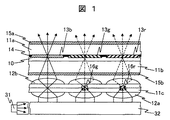
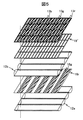
本発明の液晶表示装置の主要な構成部材とその機能を、図1に模式的に示す。 The main structural members and functions of the liquid crystal display device of the present invention are schematically shown in FIG.
図1に記載の液晶表示装置は、導光体32,光変換層,液晶表示パネルが順次積層されており、導光体32の側面には青色光を出射する光源31が配置されている。光源31は青色発光素子(青色LED)であり、可視光域の中でも短波長域の青色光を発光する。導光体32はホログラムやブレーズグレーティング(回折格子)などの分散素子を備え、その反射作用や回折作用により一方側面に配置された光源31からの青色光を液晶表示パネルの基板法線方向に向ける作用を有する。
In the liquid crystal display device illustrated in FIG. 1, a
図1中では、青色の光の光路を実線で、緑色の光の光路を一点鎖線で、赤色の光の光路を破線で示した。光変換層は、青色の光源光の一部を緑色光,赤色光に変換する。液晶表示パネルは複数の画素を有し、それぞれ青色表示,赤色表示,緑色表示を行うが、光変換層は各表示色の画素に対応する色の光を集光する作用を有する。 In FIG. 1, the optical path of blue light is indicated by a solid line, the optical path of green light is indicated by an alternate long and short dash line, and the optical path of red light is indicated by a broken line. The light conversion layer converts part of the blue light source light into green light and red light. The liquid crystal display panel has a plurality of pixels and performs blue display, red display, and green display, respectively. The light conversion layer has a function of condensing light of colors corresponding to pixels of each display color.
なお本実施例では、光変換層は、複数のレンズが配置された第一のマイクロレンズアレイ12aと、第三の基板11cと、蛍光体層(緑色の蛍光体16g,赤色の蛍光体16r)と、複数のレンズが配置された第二のマイクロレンズアレイ12bとが順次積層されて形成された構成である。また液晶パネルは、一対の基板(第一の基板11a,第二の基板
11b)と、その一対の基板で挟持された液晶層10と、一対の基板を挟持する一対の偏光板(第一の偏光板15a,第二の偏光板15b)と、カラーフィルタ(青のカラーフィルタ13b,緑のカラーフィルタ13g,赤のカラーフィルタ13r)と、ブラックマトリクス14とを有する構成とする。
In this embodiment, the light conversion layer includes a
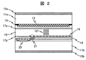
図2に液晶表示パネルの1画素の断面図の一例を示す。液晶表示パネルは第一の基板
11aと第二の基板11bと液晶層10からなり、第一の基板11aと第二の基板11bは液晶層10を挟持する。第一の基板11aと第二の基板11bは液晶層10に近接する面上に液晶層10の封入された液晶分子10′の配向状態を安定化するための一対の配向膜(第一の配向膜17a,第二の配向膜17b)を備える。また、第一の基板11aと第二の基板11bの一方もしくは両方に液晶層10に電圧を印加するための手段を備える。
FIG. 2 shows an example of a cross-sectional view of one pixel of a liquid crystal display panel. The liquid crystal display panel includes a
第一の基板11aは透明性に優れ、かつイオン性不純物の含有が少ないホウケイサンガラス製であり、厚さは約400nmである。第一の基板11aは液晶層10に近接する側より第一の配向膜17a,平坦化膜,カラーフィルタ13,ブラックマトリクス14が積層されている。第一の配向膜17aはポリイミド系の有機高分子膜であり、ラビング方法により配向処理されており、液晶層10に約2度のプレチルト角を付与する所謂水平配向膜である。カラーフィルタ13は赤色,緑色,青色を呈するストライプ状の各部分が繰り返し配列された平面構造を有する。ブラックマトリクス14は黒色レジストからなり、画素境界部に対応するように格子状の平面分布構造を有する。
The
第二の基板11bは第一の基板11a同様ホウケイサンガラス製であり、厚さは約400μmである。第一の基板11aは液晶層10に近接する側より順に、主に第二の配向膜
17b,画素電極19,層間絶縁膜,共通電極18,走査配線,信号配線,アクティブ素子20、を備える。第二の配向膜17bは、第一の配向膜17aと同様にポリイミド系の有機高分子膜である。画素電極19と共通電極18はいずれも透明性と導電性を兼ね備えたインジウム錫酸化物(Indium Tin Oxide、ITO)であり、層厚は100nmである。両者は窒化珪素(SiN)製の層間絶縁膜によって隔たれており、層間絶縁膜の層厚は
500nmである。画素電極19の平面形状は櫛歯状であるのに対し、共通電極18は各画素の全面に渡って分布しており、電圧印加時に画素電極19と共通電極18の間にはアーチ状の電界が形成される。アーチ状の電界は液晶層10に平行な成分を有する所謂横電界であり、電界は近接する液晶層中にはみ出して分布することにより、液晶層10の液晶分子の配向状態を変形するIPS(In Plane Switching)方式液晶表示パネルである。
IPS方式液晶表示パネルでは電圧印加に伴う液晶層のチルト角増大が少ないため、視角方向での階調表示特性に優れた広視野角の表示が得られる。画素電極19と共通電極18が重畳する部分は液晶層10に対して並列に結合しているため、保持容量として機能する。
The
In the IPS liquid crystal display panel, the increase in tilt angle of the liquid crystal layer due to voltage application is small, so that a wide viewing angle display excellent in gradation display characteristics in the viewing angle direction can be obtained. Since the portion where the
信号配線と走査配線は互いに交差し、信号配線と走査配線の交差部の近傍にはそれぞれアクティブ素子20を有し、画素電極19と1対1に対応している。画素電極19にはコンタクトホール21によりアクティブ素子20を介して信号配線より電位が付与され、アクティブ素子20の動作は走査配線により制御される。アクティブ素子20は薄膜トランジスタであり、そのチャネル部は電子移動度の比較的高いポリシリコン層から成る。ポリシリコン層はCVD(Chemical Vapor Deposition) 法で形成したアモルファスシリコン層をレーザー光線で加熱焼成して形成される。各画素電極は互いに独立制御され、図3に示したように長方形状であり、かつ第二の基板11b上に格子状に配置されている。
The signal wiring and the scanning wiring intersect each other, and each has an
液晶層10は室温を含む広い温度範囲でネマチック相を示し、液晶分子の配向方向の誘電率がその垂直方向よりも大きい正の誘電率異方性を示す。なおかつ、液晶層10は高抵抗を示すので、アクティブ素子20がオフとなる保持期間中においても電圧低下が十分に少ない。第一の配向膜17aと第二の配向膜17bのラビング処理方向を反平行としたことにより、液晶層10をホモジニアス配向とする。その配向方向は信号電極(櫛歯状)の櫛歯方向に対して15度を成し、電圧印加時に発生する横電界に対して75度をなす。
The
第一の基板11aと第二の基板11bの外側には第一の偏光板15aと第二の偏光板
15bを配置し、一対の基板を挟持しており、第一の偏光板15aと第二の偏光板15bはヨウ素系色素を含み、その2色性で自然光を直線偏光に変換する。ヨウ素系色素の配向方向が吸収軸であり、第一の偏光板15aと第二の偏光板15bの吸収軸は互いに直交し、かつ第一の偏光板15aの吸収軸は液晶配向方向に平行である。
A first
光変換層は、図1に示したように導光体32に近接する側より第一のマイクロレンズアレイ12a,第三の基板11c,蛍光体16,第二のマイクロレンズアレイ12bが順次積層された構造である。第一のマイクロレンズアレイ12bは第三の基板11c上にストライプ状に分布しており、押し型加工,印刷法、もしくはフォトリソグラフィーにより形成する。押し型加工では第三の基板11c上に樹脂層を形成,過熱して軟化させた状態で金型を押し当てて、凸状断面を形成する。印刷法では、溶融状態にある樹脂もしくは樹脂溶液を滴下して形成する。フォトリソグラフィーではレジストをストライプ状に加工した後、これを加熱溶融させ、メニスカスを形成した状態で焼成して固化する。このうち、金型を用いた押し型加工は最も加工精度が高いとう特徴を有し、集光性に優れたマイクロレンズを作成可能である。また、印刷法は最も低コストであり、多品種対応が可能である。
As shown in FIG. 1, the
蛍光体16は、第一のマイクロレンズアレイ12aの焦点を中心とした領域に形成する。具体的には、第一のマイクロレンズアレイ12aはその焦点が第二のマイクロレンズアレイ12bが近接する第三の基板11cの平面上に位置するように設計する。すなわち、第三の基板11c法線に平行な方向から第一のマイクロレンズアレイ12aに単色の平行光を入射した場合、理想的には第二のマイクロレンズアレイ12bが近接する第三の基板11cの平面上に集光する。この時、第二のマイクロレンズアレイ12bが近接する第三の基板11cの平面上の、光源からの青色光が集光する部分を中心とした領域に蛍光体を形成する。
The
蛍光体層は光源31である青色光を吸収して蛍光を発光する必要があり、青色光を吸収する有機蛍光体,無機蛍光体がそれぞれ開発されている。青色吸収の緑色発光無機蛍光体には、例えば(Y,Gd)3(Ai,Ga)5O12:Tb3+が利用可能である。青色吸収の赤色発光無機蛍光体には、例えば(Ca,Sr,Zn)S:Eu3+,(Y,Gd)2O2S:Eu3+が利用可能である。青色吸収の緑色発光有機蛍光体には、例えばクマリン系色素やナフタルイミド系色素が利用可能である。青色吸収の赤色発光有機蛍光体には、例えばピリミジン系色素,ローダミン系色素,オキサジン系色素が利用可能である。現状では有機蛍光体の方が高い発光効率を示す傾向にあるが、耐候性では無機蛍光体の方が優れている。
The phosphor layer needs to absorb the blue light as the
青色表示には青色発光の光源光をそのまま用いることができるので、青色表示画素に相当する第一のマイクロレンズアレイ12aの焦点上には蛍光体を配置しなくても良い。この場合、蛍光体層は赤色の蛍光体16rと緑色の蛍光体16gだけで構成する。あるいはまた、青色表示の色調を変えるために、青色表示画素に相当する第一のマイクロレンズアレイ12aの焦点上に青色のカラーフィルタを配置しても良い。
Since blue light source light can be used as it is for blue display, it is not necessary to arrange a phosphor on the focal point of the
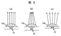
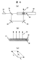
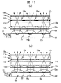
蛍光体層の上面に平坦化膜を形成した後に第二のマイクロレンズアレイ12bを形成する。図3(a)に示した様に、蛍光体16の位置が第二のマイクロレンズアレイ12bの焦点と一致すれば、蛍光体層の光は第二のマイクロレンズアレイ12bにより平行光に変換される。図3(b)に示した様に、蛍光体16の位置がその焦点よりも第二のマイクロレンズアレイ12bから離れていれば、蛍光体層の光は第二のマイクロレンズアレイ12bにより収束光に変換される。あるいはまた、図3(c)に示した様に、蛍光体16の位置がその焦点よりも第二のマイクロレンズアレイ12bに近ければ、蛍光体層の光は第二のマイクロレンズアレイ12bにより発散光に変換される。
After the planarization film is formed on the upper surface of the phosphor layer, the
つまり、対応する画素の中心部に蛍光光を集光するためには、図3(b)に示した様に蛍光体層は第二のマイクロレンズアレイ12bの焦点位置よりも第二のマイクロレンズアレイ12bから離れた位置に配置する方がより好ましい。第一のマイクロレンズアレイ
12bの平面分布をストライプ状にしたため、これに対応する第二のマイクロレンズアレイ12bの平面分布もストライプ状とした。
That is, in order to collect fluorescent light at the center of the corresponding pixel, as shown in FIG. 3B, the phosphor layer has a second microlens rather than the focal position of the
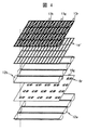
第一のマイクロレンズアレイ12aと、蛍光体層と、第二のマイクロレンズアレイ12bと、第二の基板11b上の画素と、第一の基板11a上のカラーフィルタの対応関係を図4,図5に示す。
FIG. 4 shows the correspondence between the
図4,図5中に示した画素19′は、走査配線と信号配線の形成する格子状(マトリクス)構造に対応し、かつ共通電極と画素電極が形成する電界の影響が及ぶ範囲の概略を示している。図4,図5中の破線は、図4,図5に示した液晶表示パネルの表示領域内の左下端部にある緑色画素の一つに注目し、その上部に配置されたカラーフィルタと、下部に配置された第二のマイクロレンズアレイ12b等との対応関係を示している。図5は、カラーフィルタ(青のカラーフィルタ13b,緑のカラーフィルタ13g,赤のカラーフィルタ13r)と蛍光体層(赤色の蛍光体16r,緑色の蛍光体16g)は各画素の長辺に平行なストライプ構造をなし、第一のマイクロレンズアレイ12aと第二のマイクロレンズアレイ12bは各画素の短辺に平行なストライプ構造をなす様に配置した例である。図4はカラーフィルタ(青のカラーフィルタ13b,緑のカラーフィルタ13g,赤のカラーフィルタ13r)は各画素の長辺に平行なストライプ構造をなし、蛍光体層(赤色の蛍光体16r,緑色の蛍光体16g)を四角形のドット状に配置した例である。尚、図4,図5では青色画素に対応する蛍光体層は配置せず、光源の青色光がそのまま入射するようにしている。
The pixel 19 'shown in FIGS. 4 and 5 corresponds to the lattice (matrix) structure formed by the scanning wiring and the signal wiring, and outlines the range to which the influence of the electric field formed by the common electrode and the pixel electrode is affected. Show. The broken line in FIGS. 4 and 5 pays attention to one of the green pixels at the lower left end in the display area of the liquid crystal display panel shown in FIGS. The correspondence relationship with the
導光体32に入射した光源光である青色光を、光変換層に向かう平行度の高い平面光源に変換するために、例えば導光体自体を体積ホログラムとしても良い。即ち、導光体を感光性部材で形成し、二方向から互いに可干渉なレーザー光線を入射して導光体内部に干渉を生じさせ、光が強めあう部分で光反応が進行して屈折率が増大する。これにより、導光体の内部に格子ベクトルkh で特徴付けられる屈折率の周期的変化を形成する。光源光の波数ベクトルをks とすると、光変換層に向かう出射光の波数ベクトルke は、ke=ks+kh を満足する。光源光は側面から導光体に入射し、出射光は導光体の法線方向に向かうことからke とks は直交するので、ke とks とkh の関係を図示すると図6(c)に示した様になる。図6(a)に示した様に、互いに可干渉なレーザー光線は、同一レーザー光源33からのレーザー光線をハーフミラー34,ミラー35等で分岐して参照光
36と物体光37を作成し、両者を導光体32内部で交差させる。一般にレーザー光は径が小さいため、交差部をスキャンすれば導光体の全面に体積ホログラムを作成可能である。図6(b)に示した様に、光変換層に向かう出射光を再生光38,光源光を参照光36とみなすことが可能であり、この点において図6(a),(b)は一般的なホログラムの作成方法と同様である。
In order to convert blue light, which is light source light incident on the
ke ,ks は波長を含んでおり、体積ホログラムの回折角度は波長に依存する。そのため、白色光が体積ホログラムに入射すれば波長に応じて角度の異なる光路に分離されるが、青色発光LEDは発光スペクトルの半値幅が50nm程度と狭く単色光に近いため、全発光の光路がほぼ同一方向に変換される。 k e and k s include the wavelength, and the diffraction angle of the volume hologram depends on the wavelength. Therefore, if white light is incident on the volume hologram, it is separated into optical paths with different angles depending on the wavelength. It is converted in almost the same direction.
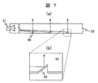
青色発光素子を有する光源31を導光体32側面のある一点に集中して配置すれば、導光体32側面に点光源が1つある状態に近似することが可能であり、導光体32の任意の点に入射する光源光の方向が一義的に定まる。これを効率的に液晶パネル法線方向に反射するため、導光体32にブレーズグレーティングを配置しても良い。図7に示した様に、ブレーズグレーティング48を導光体32底部に配置する場合には、アルミなどの高反射率の金属層39を蒸着し、液晶表示パネル法線方向に対して正反射条件を満足する角度に設定すれば、各ブレーズグレーティング48から法線方向に光源光が反射されるため、コリメート性に優れた平面光源が得られる。このように単色光に近い青色光をホログラムやブレーズグレーティングにより光路変換するため、平行度の良好な平面光源が得られる。そのため、マイクロレンズの集光効果を十分に利用できる。
If the
以上のように一対のマイクロレンズアレイの間に蛍光体を配置したことにより、蛍光体を用いながらその光散乱による光路の拡散を防止することができ、なおかつ対応する液晶パネル上の画素内に集光できる。また青色発光を蛍光体で緑色,赤色に変換し、マイクロレンズで対応する表示色の画素に集光することが可能になる。従来の主流な液晶表示装置では青色発光を黄色蛍光体で一部を黄色の蛍光に変換し、これを赤,青,緑のカラーフィルタで吸収して色表示を行っていた。このうち、特に後者の過程において生じるカラーフィルタの吸収による光損失が大きく、効率低下の原因になっていた。本発明の蛍光体の発光効率はカラーフィルタの透過効率に比較して高いため、より高効率の表示が得られる。 By arranging the phosphor between the pair of microlens arrays as described above, it is possible to prevent diffusion of the light path due to light scattering while using the phosphor, and to collect the light in the corresponding pixels on the liquid crystal panel. Can shine. Also, blue light can be converted into green and red with a phosphor, and can be condensed onto the corresponding display color pixel with a microlens. In a conventional mainstream liquid crystal display device, blue light is converted into yellow fluorescent light by a yellow phosphor and a part of it is converted into yellow fluorescent light, and this is absorbed by red, blue and green color filters to perform color display. Among these, the light loss due to the absorption of the color filter that occurs particularly in the latter process is large, which causes the efficiency to decrease. Since the luminous efficiency of the phosphor of the present invention is higher than the transmission efficiency of the color filter, a more efficient display can be obtained.
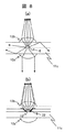
蛍光体層の蛍光は、蛍光体層を中心にして等方的に広がる性質を有する。蛍光体層が発した蛍光の典型的な光路のいくつかを図8(a)に示す。 The fluorescence of the phosphor layer has the property of spreading isotropically around the phosphor layer. FIG. 8A shows some typical optical paths of fluorescence emitted from the phosphor layer.
第二のマイクロレンズアレイ12bのある前面に向かう蛍光成分の他にも、第一のマイクロレンズアレイ12a側のある後方に向かう蛍光成分も存在する。あるいはまた側面に向かう蛍光成分も存在し、光変換層の内部で多重反射を繰り返す。これら側面、後方に向かう蛍光成分は効率低下の原因となり、その他にも迷光となって自らの色と対応しない画素に入射すれば色純度低下の原因になることもある。
In addition to the fluorescent component toward the front surface with the
本実施例では、効率低下と迷光の発生を防ぐために、蛍光体16の周辺に高反射率の金属層からなる蛍光体光反射層22を配置した。側面に向かう蛍光成分が蛍光体光反射層
22に入射するように、蛍光体16の側面に蛍光体光反射層22を配置する。また、後方からは光源光が入射するが、これを妨げず、かつ後方に向かう蛍光成分がなるだけ多く蛍光体光反射層22に入射するように、後方にも部分的に蛍光体光反射層22を配置する。
In the present embodiment, in order to prevent the efficiency reduction and the generation of stray light, the phosphor
具体的には、図8(b)に示したように、第三の基板11c平面に対して約45度の傾斜を有する蛍光体光反射層22を、各蛍光体層の周囲に配置する。蛍光体光反射層22は高反射率の金属膜で形成する。側面に向かう蛍光成分は蛍光体光反射層22で反射されて蛍光体層に戻されるため、側面に向かう光は発生しない。また、後方に向かう光の大部分も蛍光体光反射層22で反射されて蛍光体層に戻されるため、効率向上と迷光防止の効果が得られる。
Specifically, as shown in FIG. 8B, the phosphor
実施例1では、蛍光体層は赤色の蛍光体16rと緑色の蛍光体16gだけで構成した。あるいはまた図9(a)に示した様に、青色表示画素に相当する第一のマイクロレンズアレイ12aの焦点上に青のカラーフィルタ13bを配置した。この場合、赤色光と緑色光は蛍光であり、蛍光体層を中心に等方的に発光するのに対し、青色光は蛍光体による拡散を受けない。そのため、液晶パネル通過後における青色光の角度分布が、赤色光や緑色光と異なる角度分布になることもある。この場合、光源自体が色調の角度変化を有することになり、視角変化による表示の色調変化が増大するため好ましくない。
In Example 1, the phosphor layer was composed of only the
本実施例では、青色光の角度分布を他の色と一致させるため、図9(b)に示した様に青色表示画素に相当する第一のマイクロレンズアレイ12aの焦点上に光散乱層23を配置した。光散乱層23には、例えば透明微粒子を含有する透明レジストを用いることができる。この場合、フォトリソグラフィーでパターンニングが可能になり、青色表示画素に相当する第一のマイクロレンズアレイの焦点上に光散乱層23を選択的に形成できる。
In this embodiment, in order to make the angle distribution of blue light coincide with other colors, the
一般に透明微粒子と透明レジストの屈折率は異なるため、両者の界面で屈折が生じる。光散乱層23内の透明微粒子の分散密度や透明微粒子の屈折率,透明レジストの厚さを適宜調節すれば、光散乱層23に蛍光体16と同じ拡散作用を付与することができる。
In general, since the refractive indexes of the transparent fine particles and the transparent resist are different, refraction occurs at the interface between them. By appropriately adjusting the dispersion density of the transparent fine particles in the
以上により、赤色光,緑色光,青色光の角度分布を互いに等しくし、視角変化による表示の色調変化を低減できる。 As described above, the angular distributions of red light, green light, and blue light can be made equal to each other, and the change in display color tone due to the change in viewing angle can be reduced.
本発明の液晶表示装置では、各画素の表示色に対応した色の光を入射するため、第一の基板11a上のカラーフィルタを除いてもカラー表示が可能になる。この場合、第一の基板の作成プロセスが減少するため、第一の基板11aの作成が容易になる。
In the liquid crystal display device of the present invention, since light of a color corresponding to the display color of each pixel is incident, color display is possible even if the color filter on the
印刷法やフォトリソグラフィーで第一のマイクロレンズアレイ12a並びに第二のマイクロレンズアレイ12bを作成する場合、複数のレンズの個々のレンズの間に平坦部を形成しなければならない。即ち、印刷法では溶融状態若しくは溶液状態の樹脂がメニスカスを形成してマイクロレンズアレイとなるが、その際近接するメニスカス間に間隙が無ければ2つのメニスカスが表面張力により一つに合体し、個々の画素に対応するマイクロレンズアレイが作成できないからである。
When the
平坦部に入射した青色発光は、蛍光体に入射せずに青色のまま液晶パネルに入射するが、本実施例のようにカラーフィルタを除いた液晶表示パネルの赤色表示画素,緑色表示画素に入射すると色純度を低下させる。これを防ぐため、例えば図10(a)に示した様に、マイクロレンズ間の平坦部にブラックマトリクス等の平坦部吸収層24を形成する。平坦部に入射した青色発光はブラックマトリクスにより吸収されるため、青色発光の直接入射による色再現範囲低下を防ぐことができる。
Blue light incident on the flat part is incident on the liquid crystal panel as blue without entering the phosphor, but incident on the red and green display pixels of the liquid crystal display panel excluding the color filter as in this embodiment. Then, the color purity is lowered. In order to prevent this, as shown in FIG. 10A, for example, a flat
あるいはまた、図10(b)に示した様に平坦部に平坦部反射層25を形成しても良い。この場合には、平坦部に入射した青色発光は平坦部反射層25で反射されるので、青色発光の直接入射による色再現範囲低下を防ぐことができる。実施例1では迷光の発生を防ぐため蛍光体光反射層22を配置したが、蛍光体光反射層22を平坦部にまで延長して分布させ、平坦部反射層25と兼用しても良い。
Alternatively, as shown in FIG. 10B, the flat portion reflection layer 25 may be formed on the flat portion. In this case, since the blue light incident on the flat portion is reflected by the flat portion reflection layer 25, it is possible to prevent a decrease in the color reproduction range due to the direct incidence of blue light emission. In the first embodiment, the phosphor
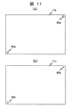
液晶表示パネルと光変換層は、対応する画素とマイクロレンズアレイが一致するように位置合わせして組み合わせる必要があるが、その際には両者に位置合わせマークが必要になる。位置合わせマークはより光吸収率の高い層で形成すれば鮮明に観察されて好都合であるが、ブラックマトリクス14に用いる黒色レジストは全可視波長で光吸収するためこれに最適である。ブラックマトリクス14に用いる黒色レジストを利用して、光変換層の端部に位置合わせマークを形成しても良い。図11(b)は光変換層の第三の基板11cの端部の2箇所に位置合わせマーク40bを形成した例であり、図11(a)はこれに対応する液晶パネル側の第二の基板11bの端部の2箇所に位置合わせマーク40aを形成した例である。位置合わせ精度を向上するためには二つの位置合わせマークは互いに離れていれば良く、図11(a),(b)では位置合わせマークは概略長方形をした光変換層および液晶表示パネルの対角線上に離れて配置している。尚、図11(a),(b)では実際よりも位置合わせマークを大きく描いてある。
The liquid crystal display panel and the light conversion layer need to be aligned and combined so that the corresponding pixels and the microlens array coincide with each other. In this case, alignment marks are required for both. If the alignment mark is formed of a layer having a higher light absorption rate, it is convenient to observe clearly, but the black resist used for the
以上のように、本実施例では液晶パネルのカラーフィルタを省略して構造を簡略化した上で、実施例1と同様の高色純度の表示特性が得られる。 As described above, in this embodiment, the color filter of the liquid crystal panel is omitted to simplify the structure, and display characteristics with high color purity similar to those in Embodiment 1 can be obtained.
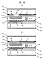
実施例1の液晶表示装置において、液晶表示パネルは透過型であったが、本実施例ではこれを半透過型液晶表示パネルとした。半透過型液晶表示パネルは一画素内に反射表示部と透過表示部を有するが、その断面の一例を図12(a)に示す。 In the liquid crystal display device of Example 1, the liquid crystal display panel was a transmissive type, but in the present example, this was a transflective liquid crystal display panel. The transflective liquid crystal display panel has a reflective display portion and a transmissive display portion in one pixel, and an example of a cross section thereof is shown in FIG.
第二の基板11bについては、反射表示部に相当する部分の共通電極18に、アルミからなる反射共通電極18′を重畳して配置する変更を加えた。第一の基板11aについては、反射表示部に相当する部分に位相差板26と段差形成層27を配置した。位相差板
26はジアクリル系液晶を光重合して形成する。位相差板26のリタデーションを310nmにし、段差形成層27で反射表示部の液晶層10のリタデーションを160nmにした。これに加えて、位相差板26の遅相軸が液晶配向方向となす角を67.5度 とすることにより、電圧無印加時に反射共通電極18′に入射する光の偏光状態を円偏光にでき、反射表示,透過表示ともノーマリクローズ表示にすることができる。
With respect to the
一画素内を反射表示部と透過表示部に面積分割したことにより、透過表示部の面積が減少する。しかし、本発明では光変換層で透過表示部に光源光を集光するので、実施例1の液晶表示装置に比較して輝度の低下はほとんど無く、その上反射表示が得られるという効果がある。 By dividing the area of one pixel into a reflective display portion and a transmissive display portion, the area of the transmissive display portion is reduced. However, in the present invention, the light conversion layer concentrates the light source light on the transmissive display portion, so that there is almost no reduction in luminance as compared with the liquid crystal display device of Example 1, and there is an effect that a reflective display can be obtained. .
反射表示部では光がカラーフィルタ13を2回通過するのに対し、透過表示部では1回だけ通過する。透過表示部と反射表示部の色再現範囲を等しくするためには、反射表示部と透過表示部のカラーフィルタ13の吸収率を変えなければならない。具体的には、図
12(a)に示した様に、反射表示部の一部にカラーフィルタ13の存在しないカラーフィルタ開口部13hを配置することにより、反射表示部の面積平均した吸収率を低下している。しかし、カラーフィルタ開口部13hの面積が設計値から外れた場合に、反射表示のカラーバランスが崩れるなどの困難があった。
In the reflective display portion, light passes through the
本発明では、透過表示部の色表示は光源光の着色で決定されるため、原理的には透過表示部にカラーフィルタ13を必要としない。そのため、反射表示向けに吸収率を最適化した反射表示用カラーフィルタ13′を、図12(b)に示した様に反射表示部と透過表示部を含む画素内の全面に均一に配置することが可能になる。
In the present invention, since the color display of the transmissive display portion is determined by the coloration of the light source light, the
反射表示用の低吸収率のカラーフィルタでは、各画素の表示色と異なる色の迷光が入射した場合に充分に吸収しきれず、色再現範囲の低下を生じる。この場合には、実施例3と同様にブラックマトリクスを配置した色変換層を用いることにより、迷光による色再現範囲の低下を防ぐことができる。 A color filter having a low absorptivity for reflective display cannot sufficiently absorb stray light having a color different from the display color of each pixel, resulting in a decrease in the color reproduction range. In this case, the color reproduction range due to stray light can be prevented from decreasing by using a color conversion layer in which a black matrix is arranged as in the third embodiment.
反射表示部に位相差板26を内蔵したことにより、液晶表示パネルの第一の基板11aおよび第二の基板11bに貼り付ける光学部材は第一の偏光板15aと、第二の偏光板
15bのみとなる。液晶表示装置全体を薄型化できるという長所を有する。
Since the
反射表示部は周囲から入射する光を反射して表示を行うため、コントラスト比は明るさによらず一定である。透過表示ではバックライト光に比較して周囲から入射する光が強い場合には界面反射によりコントラスト比が低下するが、反射表示ではこの様な場合でもコントラスト比の低下が生じない。そのため、日中の屋外など明るい環境下では透過表示よりも良好な表示が得られる。 Since the reflective display unit performs display by reflecting light incident from the surroundings, the contrast ratio is constant regardless of the brightness. In transmissive display, when the incident light from the surroundings is stronger than the backlight light, the contrast ratio decreases due to interface reflection. However, in the reflective display, the contrast ratio does not decrease even in such a case. Therefore, a display better than the transmissive display can be obtained in a bright environment such as outdoors in the daytime.
以上のように、本実施例では液晶表示パネルを半透過型としたことにより、実施例1と同様の透過表示輝度を確保した上で、明所における視認性を向上できる。 As described above, in this embodiment, the liquid crystal display panel is a transflective type, so that it is possible to improve the visibility in a bright place while ensuring the same transmissive display luminance as in the first embodiment.
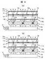
本実施例では他の実施例とは構造が異なる光変換層の一例を示す。実施例1では液晶表示パネルを構成する第一の基板11aと第二の基板11bの他に、光変換層に別途第三の基板11cを用いた。本実施例では第三の基板11cを用いずに、第一のマイクロレンズアレイ12aと蛍光体層を導光体上に形成し、第二のマイクロレンズアレイ12bを第二の基板11b上に形成した。
In this embodiment, an example of a light conversion layer having a structure different from that of the other embodiments is shown. In Example 1, in addition to the
本実施例の液晶表示装置の一構成例を図13(a)に示す。蛍光体層と蛍光体光反射層22を導光体上面に配置しており、蛍光体層の上層に液晶パネルが配置された側に対して断面が凸形状のレンズを有する第一のマイクロレンズアレイ12aを配置している。導光体32側面の光源31を発した青色光は、導光体32の内部を多重反射するうちに蛍光体層に入射して蛍光となる。蛍光は蛍光体層を中心に等方的に広がるが、蛍光体層は第一のマイクロレンズアレイ12aの焦点に位置しており、蛍光のうち前方に向かう成分は第一のマイクロレンズアレイ12aに入射して、これにより平行光に変換される。後方に向かう成分の一部と側面に向かう成分は蛍光体光反射層22によって反射されて前方に向かい、その後第一のマイクロレンズアレイ12aに入射して平行光に変換される。蛍光は第二の偏光板15bを通過してその後、導光体32が配置された側に対して断面が凸形状のレンズを有する第二のマイクロレンズアレイ12bに入射する。ここで第二のマイクロレンズアレイ12bによる集光作用を受け、対応する画素の中央部に集光される。この場合、第二のマイクロレンズアレイ12bはほぼ平行光となって入射した蛍光を、第二の基板
11bを介して存在する画素中心近傍に集光する。そのため、第二のマイクロレンズアレイ12bの焦点距離は第一のマイクロレンズアレイ12aに比較して著しく長いことが特徴である。
One structural example of the liquid crystal display device of a present Example is shown to Fig.13 (a). A first microlens having a phosphor layer and a phosphor
この場合、液晶表示パネルと導光体32の位置合わせが必要になるので、導光体32の端部と液晶表示パネルの端部に位置合わせマークを形成しても良い。これは上述した図
11(a)(b)と同様である。
In this case, since alignment between the liquid crystal display panel and the
光源31からの青色光の蛍光体層への入射効率を向上するためには、図13(b)に示した様に蛍光体層の下面にブレーズグレーティング48を配置する。実施例1にて説明したように、ブレーズグレーティング48は光源光を導光体32の法線方向に反射する様に設計可能である。ブレーズグレーティング48の直上に蛍光体層が有れば、ブレーズグレーティング48で反射した光源光が蛍光体層に直接入射することになる。
In order to improve the incidence efficiency of blue light from the
図13(a),(b)では青色表示画素に対応する光変換層には上述した光散乱層を配置していないが、実施例3で説明したのと同様の理由により、光源自体が色調の角度変化を示す場合がある。本実施例の構成においても、青色表示画素に対応する光変換層に光散乱層を配置すれば、同様にして光源自体が色調の角度変化を解消できる。 In FIGS. 13A and 13B, the light scattering layer described above is not disposed in the light conversion layer corresponding to the blue display pixel. However, for the same reason as described in Example 3, the light source itself has a color tone. May show a change in angle. Also in the configuration of the present embodiment, if the light scattering layer is arranged in the light conversion layer corresponding to the blue display pixel, the light source itself can similarly cancel the color tone angle change.
本実施例では第二のマイクロレンズアレイ12bの外側に光学フィルムを貼り付けるが、凹凸面上に貼り付けるため、粘着力不足になる場合がある。第二の偏光板15bをグリッドワイア偏光板として液晶パネルの内側に配置すれば、第二のマイクロレンズアレイ
12b上に光学部材を貼り付ける必要がなくなる。グリッドワイア偏光板は光の波長以下のピッチでスリットを形成した金属膜であり、スリットの垂直方向には金属膜の自由電子が動けないことから、スリット方向の直線偏光成分を反射し、スリット垂直方向の直線偏光成分を通過する性質を示す。
In this embodiment, an optical film is attached to the outside of the
以上の様に、第三の基板11cを用いないより薄型軽量な構造にて、実施例1と同様に高効率の液晶表示装置を実現した。
As described above, a highly efficient liquid crystal display device was realized in the same manner as in Example 1 with a thinner and lighter structure without using the
実施例1では第一のマイクロレンズアレイ12aと第二のマイクロレンズアレイ12bをストライプ状に形成したが、マイクロレンズアレイの形状はこれに限定されず、例えば個々のマイクロレンズを球面にしてハニカム状に配列しても良い。
In the first embodiment, the
図14は第一のマイクロレンズアレイ12aと蛍光体層と第二のマイクロレンズアレイ12bと画素とカラーフィルタの分布を法線方向から観察した図である。第一のマイクロレンズアレイ12aと第二のマイクロレンズアレイ12bの形状はいずれも円状とし、第一のマイクロレンズアレイ12aの中心と、これより小さい正方形ドット状の蛍光体層の分布の中心と、第二のマイクロレンズアレイ12bの中心が法線方向から見て一致するように積層した。一方で、画素とカラーフィルタはストライプ配列である。この場合にも、図14に示した様にマイクロレンズアレイの繰り返し周期を画素短辺の長さの2倍にすれば組み合わせることが可能である。各画素内において蛍光および光源光が集光される部分は画素中心からずれることになるが、マイクロレンズアレイの集光作用が充分であれば、各色の蛍光および光源光を対応する表示色の画素に集光できる。
FIG. 14 is a diagram in which the distribution of the
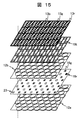
ストライプ配列の長方形画素に円形ハニカム配列のマイクロレンズアレイを組み合わせ、かつ各画素を半透過型とすることも考えられる。この場合には、各画素内において蛍光および光源光が集光される部分に透過表示部を配置すべきであり、図15に示した様に透過部画素電極19tを画素中心からずらした位置に互い違いに配置した。これにより、一画素の一定割合を反射型表示とした半透過型液晶でありながらも、全透過型と同様の透過表示効率を得ることができる。
It is also conceivable to combine a microlens array having a circular honeycomb array with a rectangular pixel having a stripe array and making each pixel a transflective type. In this case, the transmissive display portion should be arranged in the portion where the fluorescence and the light source light are condensed in each pixel, and the transmissive
図14,図15に示したストライプ配列画素の他にも、各画素の形状を正方形にしてかつデルタ配列にした場合には、ハニカム配列の方が一画素に集められる光量が増大して効率が向上するためより好ましい。 In addition to the stripe arrangement pixels shown in FIG. 14 and FIG. 15, when the shape of each pixel is a square and a delta arrangement, the honeycomb arrangement increases the amount of light collected in one pixel and increases the efficiency. It is more preferable because it improves.
実施例1では液晶表示パネルを互いに異なる層に形成された櫛歯状の画素電極19と平面ベタ状の共通電極18間に電界を印加するIPS方式液晶表示パネルとした。これ以外にも、櫛歯状の画素電極と櫛歯状の共通電極の間に横電界を形成するIPS方式液晶表示パネルとしても良い。この場合にも、実施例1と同様に視角方向での階調表示特性に優れた広視野角の表示が得られる。
In the first embodiment, the liquid crystal display panel is an IPS liquid crystal display panel in which an electric field is applied between the comb-
あるいはまた、共通電極18を第一の基板11aの液晶層10に近接する面上に形成し、共通電極18と画素電極19をいずれも平面状とし、第一の基板11a並びに第二の基板11bの法線方向に電界を印加する所謂縦電界方式としても良い。液晶層10はツイスト角が90度のツイステッドネマチック方式でも良く、ホモジニアス配向の電界複屈折方式にしても良い。IPS方式のような微細な電極加工が不必要なため、量産性に優れている。縦電界方式を半透過表示とするには、第一の基板11aと第一の偏光板15a、並びに第二の偏光板15bと第二の基板11bの間に複数の位相差板を配置して、かつ暗表示時に反射電極に到達する光の偏光状態が円偏光になるように遅相軸角度とΔndを設定すれば良い。これにより、液晶表示パネルの内側に位相差層を形成せずに半透過表示が得られるという利点がある。
Alternatively, the
各色の蛍光並びに光源光を対応する表示色の画素に選択的に入射することにより、これらの液晶表示パネルとの組み合わせにおいてもより高効率の表示が得られる。 By selectively making each color fluorescent light and light source light incident on the corresponding display color pixel, a more efficient display can be obtained even in combination with these liquid crystal display panels.
10 液晶層
10′ 液晶分子
11a 第一の基板
11b 第二の基板
12a 第一のマイクロレンズアレイ
12b 第二のマイクロレンズアレイ
13 カラーフィルタ
13r 赤のカラーフィルタ
13g 緑のカラーフィルタ
13b 青のカラーフィルタ
13h カラーフィルタ開口部
13′ 反射表示用カラーフィルタ
14 ブラックマトリクス
15a 第一の偏光板
15b 第二の偏光板
16 蛍光体
16r 赤色の蛍光体
16g 緑色の蛍光体
17a 第一の配向膜
17b 第二の配向膜
18 共通電極
18′ 反射共通電極
19 画素電極
19t 透過部画素電極
20 アクティブ素子
21 コンタクトホール
22 蛍光体光反射層
23 光散乱層
24 平坦部吸収層
25 平坦部反射層
26 位相差板
27 段差形成層
31 光源
32 導光体
33 レーザー光源
34 ハーフミラー
35 ミラー
36 参照光
37 物体光
38 再生光
39 金属層
40a,40b 位置合わせマーク
48 ブレーズグレーティング
10 liquid crystal layer 10 '
Claims (17)
を有して複数の画素を備える液晶パネルと、
青色光を出射する光源と、
前記液晶パネルと前記光源間に配置され、複数のレンズが配置された第一のマイクロレンズアレイと、複数のレンズが配置された第二のマイクロレンズアレイと、前記第一のマイクロレンズアレイと前記第二のマイクロレンズアレイ間に配置された蛍光体層と、を有する光変換層と、を有し、
前記光変換層の前記第一のマイクロレンズアレイは、前記光源からの青色光を前記蛍光体層に集光する機能を有し、
前記光変換層の前記第二のマイクロレンズアレイは、前記蛍光体層から出射された蛍光光、または前記光源からの青色光を、前記液晶パネル内の対応する画素に集光する機能を有し、
前記蛍光体層は、赤色蛍光体と、緑色蛍光体とを有し、
前記赤色蛍光体は、前記複数の画素のうち赤色表示を行う画素に対応して配置され、
前記緑色蛍光体は、前記複数の画素のうち緑色表示を行う画素に対応して配置された液晶表示装置。 A first substrate, a second substrate, a liquid crystal layer sandwiched between the first substrate and the second substrate,
A liquid crystal panel comprising a plurality of pixels have a,
A light source that emits blue light;
A first microlens array in which a plurality of lenses are arranged, a second microlens array in which a plurality of lenses are arranged, the first microlens array, and the a phosphor layer disposed between the second microlens array, and a light conversion layer having a possess,
The first microlens array of the light conversion layer has a function of condensing blue light from the light source on the phosphor layer,
The second microlens array of the light conversion layer has a function of condensing fluorescent light emitted from the phosphor layer or blue light from the light source onto a corresponding pixel in the liquid crystal panel. ,
The phosphor layer has a red phosphor and a green phosphor,
The red phosphor is disposed corresponding to a pixel that performs red display among the plurality of pixels,
The green phosphor is a liquid crystal display device arranged corresponding to a pixel that performs green display among the plurality of pixels.
前記光源と前記光変換層間に配置され、前記光源からの青色光を前記光変換層へ出射する導光体を有する液晶表示装置。 The liquid crystal display device according to claim 1 .
A liquid crystal display device having a light guide disposed between the light source and the light conversion layer and emitting blue light from the light source to the light conversion layer.
前記第一のマイクロレンズアレイの前記複数のレンズの断面形状は、前記光源が配置された側に対して凸形状であり、
前記第二のマイクロレンズアレイの前記複数のレンズの断面形状は、前記液晶パネルが配置された側に対して凸形状である液晶表示装置。 The liquid crystal display device according to claim 1 .
The cross-sectional shape of the plurality of lenses of the first microlens array is a convex shape with respect to the side on which the light source is disposed,
The cross-sectional shape of the plurality of lenses of the second microlens array is a liquid crystal display device that is convex with respect to the side on which the liquid crystal panel is disposed.
前記液晶パネルは、カラーフィルタを有し、
前記赤色蛍光体と、前記緑色蛍光体は、前記複数の画素の各画素に位置する前記カラーフィルタの色に対応して配置された液晶表示装置。 The liquid crystal display device according to claim 1 .
The liquid crystal panel has a color filter,
And the red phosphor, the green phosphor, a liquid crystal display device which is placed in correspondence with the color of the color filter located at each pixel of the plurality of pixels.
前記第一のマイクロレンズアレイと前記第二のマイクロレンズアレイは同一の平面分布を示す液晶表示装置。 The liquid crystal display device according to claim 1 .
The liquid crystal display device in which the first microlens array and the second microlens array exhibit the same planar distribution.
前記光源は、青色発光素子を有し、
前記青色発光素子は、前記導光体の一方側面に配置され、
前記導光体は、ホログラムまたはブレーズグレーティングが配置され、
前記ホログラムまたはブレーズグレーティングは、前記青色発光素子の発光を面状光源に変換して前記液晶パネルの法線方向に向かわせる液晶表示装置。 The liquid crystal display device according to claim 2 .
The light source has a blue light emitting element,
The blue light emitting element is disposed on one side of the light guide,
The light guide is provided with a hologram or a blazed grating,
The hologram or blazed grating is a liquid crystal display device that converts light emitted from the blue light emitting element into a planar light source and directs it in a normal direction of the liquid crystal panel.
前記蛍光体層は、前記第一のマイクロレンズアレイの焦点位置に配置された液晶表示装置。 The liquid crystal display device according to claim 1 .
The phosphor layer is a liquid crystal display device disposed at a focal position of the first microlens array.
前記蛍光体層は、前記第二のマイクロレンズアレイの焦点位置よりも前記第二のマイクロレンズアレイから離れた位置に配置された液晶表示装置。 The liquid crystal display device according to claim 1 .
The phosphor layer is a liquid crystal display device arranged at a position farther from the second microlens array than a focal position of the second microlens array.
前記第一のマイクロレンズアレイ及び前記第二のマイクロレンズアレイの前記複数のレンズのレンズ間に平坦部を有し、前記第一のマイクロレンズアレイと前記第二のマイクロレンズアレイ間に配置され、前記平坦部に対応する位置に平坦部吸収層若しくは平坦部反射層を配置した液晶表示装置。 The liquid crystal display device according to claim 1 .
A flat portion between the lenses of the plurality of lenses of the first microlens array and the second microlens array, and disposed between the first microlens array and the second microlens array; A liquid crystal display device in which a flat portion absorbing layer or a flat portion reflecting layer is disposed at a position corresponding to the flat portion.
前記光変換層と前記液晶パネルの位置合わせのためのマークを、前記光変換層上及び前記液晶パネル上に形成した液晶表示装置。 The liquid crystal display device according to claim 1.
A liquid crystal display device in which marks for alignment between the light conversion layer and the liquid crystal panel are formed on the light conversion layer and the liquid crystal panel.
前記光変換層は、第三の基板を有し、
前記第一のマイクロレンズアレイと前記第二のマイクロレンズアレイは、前記第三の基板の異なる側に互いに形成され、前記蛍光体層は、前記第三の基板上に形成された液晶表示装置。 The liquid crystal display device according to claim 1 .
The light conversion layer has a third substrate,
The first microlens array and the second microlens array are formed on different sides of the third substrate, and the phosphor layer is formed on the third substrate.
前記液晶パネルが備える前記画素は、櫛歯状またはスリット状の画素電極と、前記画素全面にわたって形成されたべた状の共通電極を有する液晶表示装置。 The liquid crystal display device according to claim 1 .
The pixel included in the liquid crystal panel is a liquid crystal display device having a comb-like or slit-like pixel electrode and a solid common electrode formed over the entire surface of the pixel.
前記液晶パネルが備える前記複数の各画素は、透過表示部と反射表示部を有する液晶表示装置。 The liquid crystal display device according to claim 1 .
Wherein said plurality of pixels where the liquid crystal panel comprises a liquid crystal display device having a reflective display portion and the transmissive display unit.
前記液晶パネルを挟持する一対の偏光板と、
青色光を出射する光源と、
前記液晶パネルと前記光源間に配置された導光体と、
前記液晶パネルと前記導光体間に配置され、複数のレンズが配置された第一のマイクロレンズアレイと、複数のレンズが配置された第二のマイクロレンズアレイと、前記第一のマイクロレンズアレイと前記導光体間に配置された蛍光体層と、を有する光変換層と、
前記導光体と前記蛍光体層間に部分的に配置される蛍光体光反射層と、を有し、
前記一対の偏光板の一方の偏光板は、前記第一のマイクロレンズアレイと前記第二のマイクロレンズアレイ間に配置され、
前記蛍光体層は、赤色蛍光体と、緑色蛍光体とを有し、
前記赤色蛍光体は、前記複数の画素のうち赤色表示を行う画素に対応して配置され、
前記緑色蛍光体は、前記複数の画素のうち緑色表示を行う画素に対応して配置され、
前記光変換層の前記第一のマイクロレンズアレイは、前記赤色蛍光体および前記緑色蛍光体からの蛍光、または前記光源からの青色光を、平行光とする機能を有し、
前記光変換層の前記第二のマイクロレンズアレイは、前記赤色蛍光体および前記緑色蛍光体から前記一方の偏光板を介して出射された蛍光光、または前記光源から前記一方の偏光板を介して出射された青色光を、前記液晶パネル内の対応する画素に集光する機能を有する液晶表示装置。 A liquid crystal panel including a first substrate, a second substrate, said a first substrate and a liquid crystal layer sandwiched between the second substrate, a plurality of pixels have a,
A pair of polarizing plates sandwiching the liquid crystal panel;
A light source that emits blue light;
A light guide disposed between the liquid crystal panel and the light source;
A first microlens array having a plurality of lenses disposed between the liquid crystal panel and the light guide, a second microlens array having a plurality of lenses disposed, and the first microlens array And a phosphor layer disposed between the light guides, and a light conversion layer,
A phosphor light reflecting layer partially disposed between the light guide and the phosphor layer,
One polarizing plate of the pair of polarizing plates is disposed between the first microlens array and the second microlens array,
The phosphor layer has a red phosphor and a green phosphor,
The red phosphor is disposed corresponding to a pixel that performs red display among the plurality of pixels,
The green phosphor is disposed corresponding to a pixel that performs green display among the plurality of pixels,
The first microlens array of the light conversion layer has a function of making fluorescence from the red phosphor and the green phosphor, or blue light from the light source into parallel light,
The second microlens array of the light conversion layer includes fluorescent light emitted from the red phosphor and the green phosphor through the one polarizing plate, or from the light source through the one polarizing plate. A liquid crystal display device having a function of condensing emitted blue light onto a corresponding pixel in the liquid crystal panel .
前記第一のマイクロレンズアレイの前記複数のレンズの断面形状は、前記液晶パネルが配置された側に対して凸形状であり、
前記第二のマイクロレンズアレイの前記複数のレンズの断面形状は、前記光源が配置された側に対して凸形状である液晶表示装置。 The liquid crystal display device according to claim 14 .
The cross-sectional shape of the plurality of lenses of the first microlens array is convex with respect to the side on which the liquid crystal panel is disposed,
The cross-sectional shape of the plurality of lenses of the second microlens array is a liquid crystal display device that is convex with respect to the side on which the light source is disposed.
前記導光体は、ブレーズグレーティングを有する液晶表示装置。 The liquid crystal display device according to claim 14 .
The light guide is a liquid crystal display device having a blazed grating.
前記液晶パネルが備える前記画素は、櫛歯状またはスリット状の画素電極と、前記画素全面にわたって形成されたべた状の共通電極を有する液晶表示装置。 The liquid crystal display device according to claim 14 .
The pixel included in the liquid crystal panel is a liquid crystal display device having a comb-like or slit-like pixel electrode and a solid common electrode formed over the entire surface of the pixel.
Priority Applications (2)
| Application Number | Priority Date | Filing Date | Title |
|---|---|---|---|
| JP2006275964A JP4851908B2 (en) | 2006-10-10 | 2006-10-10 | Liquid crystal display |
| US11/869,900 US7639320B2 (en) | 2006-10-10 | 2007-10-10 | Liquid crystal display device |
Applications Claiming Priority (1)
| Application Number | Priority Date | Filing Date | Title |
|---|---|---|---|
| JP2006275964A JP4851908B2 (en) | 2006-10-10 | 2006-10-10 | Liquid crystal display |
Publications (2)
| Publication Number | Publication Date |
|---|---|
| JP2008096547A JP2008096547A (en) | 2008-04-24 |
| JP4851908B2 true JP4851908B2 (en) | 2012-01-11 |
Family
ID=39274690
Family Applications (1)
| Application Number | Title | Priority Date | Filing Date |
|---|---|---|---|
| JP2006275964A Expired - Fee Related JP4851908B2 (en) | 2006-10-10 | 2006-10-10 | Liquid crystal display |
Country Status (2)
| Country | Link |
|---|---|
| US (1) | US7639320B2 (en) |
| JP (1) | JP4851908B2 (en) |
Families Citing this family (36)
| Publication number | Priority date | Publication date | Assignee | Title |
|---|---|---|---|---|
| US20090218582A1 (en) * | 2008-02-28 | 2009-09-03 | Kang Wei-Hung | Optical device and method of fabricating the same |
| CN201174014Y (en) * | 2008-04-10 | 2008-12-31 | 北京京东方光电科技有限公司 | Back light module unit |
| EP2314074A4 (en) * | 2008-07-29 | 2013-06-26 | Thomson Licensing | FILTERING DISPLAY CHARACTERIZATION |
| JP4848404B2 (en) * | 2008-09-04 | 2011-12-28 | 株式会社 日立ディスプレイズ | Liquid crystal display element and liquid crystal display device |
| US20100214282A1 (en) | 2009-02-24 | 2010-08-26 | Dolby Laboratories Licensing Corporation | Apparatus for providing light source modulation in dual modulator displays |
| RU2011143802A (en) * | 2009-03-30 | 2013-05-10 | Шарп Кабусики Кайся | DISPLAY PANEL AND DISPLAY DEVICE |
| US20110216266A1 (en) * | 2010-03-02 | 2011-09-08 | Microsoft Corporation | Wedge backlight with diffraction grating |
| JP5607430B2 (en) * | 2010-06-10 | 2014-10-15 | 株式会社ジャパンディスプレイ | Stereoscopic display device and electronic device |
| US20120120467A1 (en) * | 2010-11-17 | 2012-05-17 | Qualcomm Mems Technologies, Inc. | Hybrid light guide with faceted and holographic light turning features |
| US8514352B2 (en) | 2010-12-10 | 2013-08-20 | Sharp Kabushiki Kaisha | Phosphor-based display |
| TWI550581B (en) | 2010-12-17 | 2016-09-21 | 杜比實驗室特許公司 | Method and apparatus for image display, computer readable storage medium, and computing device |
| KR101851726B1 (en) * | 2011-11-23 | 2018-04-24 | 엘지이노텍 주식회사 | Display device |
| KR101360643B1 (en) | 2012-05-09 | 2014-02-10 | 엘지이노텍 주식회사 | Light converting member, light emitting device and display device having the same |
| KR102118309B1 (en) | 2012-09-19 | 2020-06-03 | 돌비 레버러토리즈 라이쎈싱 코오포레이션 | Quantum dot/remote phosphor display system improvements |
| WO2014103093A1 (en) * | 2012-12-26 | 2014-07-03 | パナソニック株式会社 | Image display device and light conversion panel used in same |
| US9436056B2 (en) * | 2013-02-06 | 2016-09-06 | E Ink Corporation | Color electro-optic displays |
| CN110060640B (en) | 2013-03-08 | 2022-04-29 | 杜比实验室特许公司 | Display system and device |
| JP6087872B2 (en) * | 2013-08-12 | 2017-03-01 | 富士フイルム株式会社 | Optical film, barrier film, light conversion member, backlight unit, and liquid crystal display device |
| EP3123240A2 (en) | 2014-03-26 | 2017-02-01 | Dolby Laboratories Licensing Corp. | Global light compensation in a variety of displays |
| EP3633663B1 (en) | 2014-08-21 | 2024-06-19 | Dolby Laboratories Licensing Corporation | Techniques for dual modulation with light conversion |
| US20160093269A1 (en) * | 2014-09-26 | 2016-03-31 | Pixtronix, Inc. | Laser-Pumped Phosphor Backlight and Methods |
| US9470925B2 (en) * | 2014-09-30 | 2016-10-18 | Shenzhen China Star Optoelectronics Technology Co., Ltd | Liquid crystal display device |
| KR101621820B1 (en) | 2014-12-29 | 2016-05-17 | 삼성전자 주식회사 | Light source, back light unit and liquid crystal display including the light source |
| CN105929591B (en) | 2016-07-08 | 2019-04-05 | 京东方科技集团股份有限公司 | Quantum dot display substrate and its manufacturing method and quantum dot display device |
| KR102712901B1 (en) | 2016-08-17 | 2024-10-07 | 삼성전자주식회사 | Display panel and display apparutus having the same |
| CN107402473B (en) * | 2017-09-25 | 2020-11-06 | 京东方科技集团股份有限公司 | Display module and display device |
| CN108051945B (en) * | 2018-01-02 | 2021-03-16 | 京东方科技集团股份有限公司 | Display assembly, liquid crystal display and electronic equipment |
| CN108415191A (en) * | 2018-03-15 | 2018-08-17 | 京东方科技集团股份有限公司 | Display device, electronic equipment and display methods |
| CN109100871B (en) * | 2018-09-14 | 2021-09-03 | 京东方科技集团股份有限公司 | Optical modulation device and spectrum detection system |
| EP3671711A1 (en) * | 2018-12-20 | 2020-06-24 | IMEC vzw | Cross-talk reduction in display with optical scanner |
| CN110646982B (en) * | 2019-10-08 | 2021-08-10 | 京东方科技集团股份有限公司 | Liquid crystal display panel, driving method thereof and display device |
| CN111175982B (en) * | 2020-02-24 | 2023-01-17 | 京东方科技集团股份有限公司 | Near-to-eye display device and wearable equipment |
| CN113534456A (en) * | 2020-04-22 | 2021-10-22 | 京东方科技集团股份有限公司 | A near-eye display device and a near-eye display device |
| CN112054131B (en) * | 2020-09-14 | 2022-09-20 | 京东方科技集团股份有限公司 | Display panel, display device and display equipment |
| CN112859347A (en) * | 2021-02-25 | 2021-05-28 | 京东方科技集团股份有限公司 | Near-to-eye display device and wearable equipment |
| CN117031814A (en) * | 2023-07-03 | 2023-11-10 | 联想(北京)有限公司 | Display device, processing method and processor |
Family Cites Families (10)
| Publication number | Priority date | Publication date | Assignee | Title |
|---|---|---|---|---|
| US4798448A (en) * | 1988-02-16 | 1989-01-17 | General Electric Company | High efficiency illumination system for display devices |
| JP3528994B2 (en) * | 1994-11-08 | 2004-05-24 | 大日本印刷株式会社 | Parallel light source for liquid crystal display device and liquid crystal display device using the same |
| JP3405087B2 (en) * | 1995-11-06 | 2003-05-12 | ソニー株式会社 | Liquid crystal display device and method of manufacturing the same |
| JPH09167513A (en) * | 1995-12-15 | 1997-06-24 | Kuraray Co Ltd | Surface light source element |
| JP2865618B2 (en) * | 1996-05-31 | 1999-03-08 | 嶋田プレシジョン株式会社 | Light guide plate and light guide plate assembly |
| JP2001133770A (en) * | 1999-11-04 | 2001-05-18 | Hitachi Ltd | Liquid crystal display |
| JP2003015122A (en) | 2001-06-27 | 2003-01-15 | Seiko Epson Corp | Liquid crystal display and electronic equipment |
| JP2003015121A (en) | 2001-06-27 | 2003-01-15 | Seiko Epson Corp | Liquid crystal display and electronic equipment |
| JP2005353650A (en) | 2004-06-08 | 2005-12-22 | Matsushita Electric Ind Co Ltd | LED light source and liquid crystal display device |
| JP2006012722A (en) * | 2004-06-29 | 2006-01-12 | Sharp Corp | Backlight device and liquid crystal display device including the same |
-
2006
- 2006-10-10 JP JP2006275964A patent/JP4851908B2/en not_active Expired - Fee Related
-
2007
- 2007-10-10 US US11/869,900 patent/US7639320B2/en not_active Expired - Fee Related
Also Published As
| Publication number | Publication date |
|---|---|
| JP2008096547A (en) | 2008-04-24 |
| US7639320B2 (en) | 2009-12-29 |
| US20080084517A1 (en) | 2008-04-10 |
Similar Documents
| Publication | Publication Date | Title |
|---|---|---|
| JP4851908B2 (en) | Liquid crystal display | |
| JP5112230B2 (en) | Liquid crystal display | |
| US8345182B2 (en) | Liquid crystal display device | |
| KR101222566B1 (en) | Display panel and display apparatus comprising the same | |
| JP4778873B2 (en) | Liquid crystal display | |
| US6469755B1 (en) | Illuminating arrangement with reflector having inclined irregularities or corrugations | |
| JP3957986B2 (en) | Reflective display device | |
| JPH10325953A (en) | Reflective and transmissive display | |
| JP3506978B2 (en) | Reflective liquid crystal display | |
| US10558083B2 (en) | Liquid crystal display module and liquid crystal display device | |
| JP2013235141A (en) | Color liquid crystal display unit | |
| CN111025728A (en) | display device | |
| US20180196302A1 (en) | Display device | |
| JP2003195275A (en) | Liquid crystal display | |
| US8531629B2 (en) | Reflective display device including polymer-dispersed liquid crystals having particular light-absorbing member | |
| JP4436752B2 (en) | Light source device and liquid crystal display device | |
| TW202430990A (en) | Optical element, manufacturing method thereof, and lighting device | |
| JP4112663B2 (en) | Liquid crystal display | |
| JP2009092972A (en) | Display device | |
| JP2000338476A (en) | Color filter substrate for reflective liquid crystal display | |
| JPH0815689A (en) | Liquid crystal display device | |
| KR101213104B1 (en) | Micro-lens array sheet and liquid crystal display using the same | |
| JP2001133777A (en) | Liquid crystal display | |
| JP2004013059A (en) | Liquid crystal display and electronic equipment | |
| JP2001209048A (en) | Liquid crystal display |
Legal Events
| Date | Code | Title | Description |
|---|---|---|---|
| A621 | Written request for application examination |
Free format text: JAPANESE INTERMEDIATE CODE: A621 Effective date: 20090225 |
|
| A521 | Written amendment |
Free format text: JAPANESE INTERMEDIATE CODE: A523 Effective date: 20090225 |
|
| RD02 | Notification of acceptance of power of attorney |
Free format text: JAPANESE INTERMEDIATE CODE: A7422 Effective date: 20100127 |
|
| RD04 | Notification of resignation of power of attorney |
Free format text: JAPANESE INTERMEDIATE CODE: A7424 Effective date: 20100301 |
|
| A711 | Notification of change in applicant |
Free format text: JAPANESE INTERMEDIATE CODE: A712 Effective date: 20110112 |
|
| A977 | Report on retrieval |
Free format text: JAPANESE INTERMEDIATE CODE: A971007 Effective date: 20110622 |
|
| A131 | Notification of reasons for refusal |
Free format text: JAPANESE INTERMEDIATE CODE: A131 Effective date: 20110705 |
|
| A521 | Written amendment |
Free format text: JAPANESE INTERMEDIATE CODE: A523 Effective date: 20110905 |
|
| TRDD | Decision of grant or rejection written | ||
| A01 | Written decision to grant a patent or to grant a registration (utility model) |
Free format text: JAPANESE INTERMEDIATE CODE: A01 Effective date: 20110927 |
|
| A01 | Written decision to grant a patent or to grant a registration (utility model) |
Free format text: JAPANESE INTERMEDIATE CODE: A01 |
|
| A61 | First payment of annual fees (during grant procedure) |
Free format text: JAPANESE INTERMEDIATE CODE: A61 Effective date: 20111021 |
|
| R150 | Certificate of patent or registration of utility model |
Ref document number: 4851908 Country of ref document: JP Free format text: JAPANESE INTERMEDIATE CODE: R150 Free format text: JAPANESE INTERMEDIATE CODE: R150 |
|
| FPAY | Renewal fee payment (event date is renewal date of database) |
Free format text: PAYMENT UNTIL: 20141028 Year of fee payment: 3 |
|
| R250 | Receipt of annual fees |
Free format text: JAPANESE INTERMEDIATE CODE: R250 |
|
| R250 | Receipt of annual fees |
Free format text: JAPANESE INTERMEDIATE CODE: R250 |
|
| R250 | Receipt of annual fees |
Free format text: JAPANESE INTERMEDIATE CODE: R250 |
|
| R250 | Receipt of annual fees |
Free format text: JAPANESE INTERMEDIATE CODE: R250 |
|
| R250 | Receipt of annual fees |
Free format text: JAPANESE INTERMEDIATE CODE: R250 |
|
| R250 | Receipt of annual fees |
Free format text: JAPANESE INTERMEDIATE CODE: R250 |
|
| LAPS | Cancellation because of no payment of annual fees |