JP4745357B2 - プリント回路基板スパークギャップ - Google Patents
プリント回路基板スパークギャップ Download PDFInfo
- Publication number
- JP4745357B2 JP4745357B2 JP2008052492A JP2008052492A JP4745357B2 JP 4745357 B2 JP4745357 B2 JP 4745357B2 JP 2008052492 A JP2008052492 A JP 2008052492A JP 2008052492 A JP2008052492 A JP 2008052492A JP 4745357 B2 JP4745357 B2 JP 4745357B2
- Authority
- JP
- Japan
- Prior art keywords
- spark gap
- smd
- conductive
- spark
- conductor
- Prior art date
- Legal status (The legal status is an assumption and is not a legal conclusion. Google has not performed a legal analysis and makes no representation as to the accuracy of the status listed.)
- Expired - Fee Related
Links
Images


Classifications
-
- H—ELECTRICITY
- H05—ELECTRIC TECHNIQUES NOT OTHERWISE PROVIDED FOR
- H05K—PRINTED CIRCUITS; CASINGS OR CONSTRUCTIONAL DETAILS OF ELECTRIC APPARATUS; MANUFACTURE OF ASSEMBLAGES OF ELECTRICAL COMPONENTS
- H05K1/00—Printed circuits
- H05K1/02—Details
- H05K1/0213—Electrical arrangements not otherwise provided for
- H05K1/0254—High voltage adaptations; Electrical insulation details; Overvoltage or electrostatic discharge protection ; Arrangements for regulating voltages or for using plural voltages
- H05K1/0257—Overvoltage protection
- H05K1/026—Spark gaps
-
- H—ELECTRICITY
- H05—ELECTRIC TECHNIQUES NOT OTHERWISE PROVIDED FOR
- H05K—PRINTED CIRCUITS; CASINGS OR CONSTRUCTIONAL DETAILS OF ELECTRIC APPARATUS; MANUFACTURE OF ASSEMBLAGES OF ELECTRICAL COMPONENTS
- H05K9/00—Screening of apparatus or components against electric or magnetic fields
-
- H—ELECTRICITY
- H01—ELECTRIC ELEMENTS
- H01T—SPARK GAPS; OVERVOLTAGE ARRESTERS USING SPARK GAPS; SPARKING PLUGS; CORONA DEVICES; GENERATING IONS TO BE INTRODUCED INTO NON-ENCLOSED GASES
- H01T4/00—Overvoltage arresters using spark gaps
- H01T4/08—Overvoltage arresters using spark gaps structurally associated with protected apparatus
-
- H—ELECTRICITY
- H05—ELECTRIC TECHNIQUES NOT OTHERWISE PROVIDED FOR
- H05K—PRINTED CIRCUITS; CASINGS OR CONSTRUCTIONAL DETAILS OF ELECTRIC APPARATUS; MANUFACTURE OF ASSEMBLAGES OF ELECTRICAL COMPONENTS
- H05K2201/00—Indexing scheme relating to printed circuits covered by H05K1/00
- H05K2201/09—Shape and layout
- H05K2201/09009—Substrate related
- H05K2201/09063—Holes or slots in insulating substrate not used for electrical connections
-
- H—ELECTRICITY
- H05—ELECTRIC TECHNIQUES NOT OTHERWISE PROVIDED FOR
- H05K—PRINTED CIRCUITS; CASINGS OR CONSTRUCTIONAL DETAILS OF ELECTRIC APPARATUS; MANUFACTURE OF ASSEMBLAGES OF ELECTRICAL COMPONENTS
- H05K2201/00—Indexing scheme relating to printed circuits covered by H05K1/00
- H05K2201/10—Details of components or other objects attached to or integrated in a printed circuit board
- H05K2201/10613—Details of electrical connections of non-printed components, e.g. special leads
- H05K2201/10621—Components characterised by their electrical contacts
- H05K2201/10636—Leadless chip, e.g. chip capacitor or resistor
-
- H—ELECTRICITY
- H05—ELECTRIC TECHNIQUES NOT OTHERWISE PROVIDED FOR
- H05K—PRINTED CIRCUITS; CASINGS OR CONSTRUCTIONAL DETAILS OF ELECTRIC APPARATUS; MANUFACTURE OF ASSEMBLAGES OF ELECTRICAL COMPONENTS
- H05K3/00—Apparatus or processes for manufacturing printed circuits
- H05K3/30—Assembling printed circuits with electric components, e.g. with resistor
- H05K3/32—Assembling printed circuits with electric components, e.g. with resistor electrically connecting electric components or wires to printed circuits
- H05K3/34—Assembling printed circuits with electric components, e.g. with resistor electrically connecting electric components or wires to printed circuits by soldering
- H05K3/341—Surface mounted components
- H05K3/3431—Leadless components
- H05K3/3442—Leadless components having edge contacts, e.g. leadless chip capacitors, chip carriers
-
- Y—GENERAL TAGGING OF NEW TECHNOLOGICAL DEVELOPMENTS; GENERAL TAGGING OF CROSS-SECTIONAL TECHNOLOGIES SPANNING OVER SEVERAL SECTIONS OF THE IPC; TECHNICAL SUBJECTS COVERED BY FORMER USPC CROSS-REFERENCE ART COLLECTIONS [XRACs] AND DIGESTS
- Y02—TECHNOLOGIES OR APPLICATIONS FOR MITIGATION OR ADAPTATION AGAINST CLIMATE CHANGE
- Y02P—CLIMATE CHANGE MITIGATION TECHNOLOGIES IN THE PRODUCTION OR PROCESSING OF GOODS
- Y02P70/00—Climate change mitigation technologies in the production process for final industrial or consumer products
- Y02P70/50—Manufacturing or production processes characterised by the final manufactured product
Description
本発明は電気回路を保護するスパークギャップに関し、より詳細にはプリント回路基板に関するスパークギャップに関する。
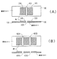
200、300 導体
210、310 表面取付デバイス(SMD)
210A,B、310A,B、510A,B SMD
220、221、320、321 はんだフィレット
230、231 導体端
400 スパークギャップ
Claims (2)
- 各々が第一の導電性表面上に配置され、第一の平坦表面を有する、少なくとも2つの第一の表面取付デバイスを有し、
第一の導電性表面および前記少なくとも2つの第一の表面取付デバイスは、所定の間隔だけ、第二の導電性表面から分離されており、前記第二の導電性表面と協働して、両導電性表面の間に電気的なアークを可能にするギャップを形成し、
前記少なくとも2つの第一の表面取付デバイスは、熱吸収部材であることを特徴とするプリント回路基板スパークギャップ。 - さらに、各々が第二の導電性表面上に配置され、第一の平坦表面を有する、1または2以上の第二の表面取付デバイスを有し、前記第二の導電性表面上の1または2以上の第二の表面取付デバイスは、所定の間隔だけ、前記第一の導電性表面上の少なくとも2つの第一の表面取付デバイスから分離されていることを特徴とする請求項1に記載のプリント回路基板スパークギャップ。
Applications Claiming Priority (2)
| Application Number | Priority Date | Filing Date | Title |
|---|---|---|---|
| US08/603,050 US5933307A (en) | 1996-02-16 | 1996-02-16 | Printed circuit board sparkgap |
| US603050 | 1996-02-16 |
Related Parent Applications (1)
| Application Number | Title | Priority Date | Filing Date |
|---|---|---|---|
| JP8348761A Division JPH09232065A (ja) | 1996-02-16 | 1996-12-26 | プリント回路基板スパークギャップ |
Publications (2)
| Publication Number | Publication Date |
|---|---|
| JP2008159597A JP2008159597A (ja) | 2008-07-10 |
| JP4745357B2 true JP4745357B2 (ja) | 2011-08-10 |
Family
ID=24413889
Family Applications (2)
| Application Number | Title | Priority Date | Filing Date |
|---|---|---|---|
| JP8348761A Pending JPH09232065A (ja) | 1996-02-16 | 1996-12-26 | プリント回路基板スパークギャップ |
| JP2008052492A Expired - Fee Related JP4745357B2 (ja) | 1996-02-16 | 2008-03-03 | プリント回路基板スパークギャップ |
Family Applications Before (1)
| Application Number | Title | Priority Date | Filing Date |
|---|---|---|---|
| JP8348761A Pending JPH09232065A (ja) | 1996-02-16 | 1996-12-26 | プリント回路基板スパークギャップ |
Country Status (12)
| Country | Link |
|---|---|
| US (1) | US5933307A (ja) |
| EP (1) | EP0790758B1 (ja) |
| JP (2) | JPH09232065A (ja) |
| KR (1) | KR100441037B1 (ja) |
| CN (1) | CN1052347C (ja) |
| BR (1) | BR9606195A (ja) |
| DE (1) | DE69633848T2 (ja) |
| HK (1) | HK1005111A1 (ja) |
| ID (1) | ID15938A (ja) |
| IN (1) | IN189905B (ja) |
| MY (1) | MY120205A (ja) |
| SG (1) | SG48504A1 (ja) |
Families Citing this family (33)
| Publication number | Priority date | Publication date | Assignee | Title |
|---|---|---|---|---|
| GB2334626B (en) * | 1998-02-20 | 2003-01-29 | Mitel Corp | Spark gap for hermetically packaged integrated circuits |
| GB2335084B (en) | 1998-02-21 | 2003-04-02 | Mitel Corp | Spark gap for high voltage integrated circuit electrostatic discharge protection |
| US7825491B2 (en) | 2005-11-22 | 2010-11-02 | Shocking Technologies, Inc. | Light-emitting device using voltage switchable dielectric material |
| AU6531600A (en) | 1999-08-27 | 2001-03-26 | Lex Kosowsky | Current carrying structure using voltage switchable dielectric material |
| US7695644B2 (en) | 1999-08-27 | 2010-04-13 | Shocking Technologies, Inc. | Device applications for voltage switchable dielectric material having high aspect ratio particles |
| US6493198B1 (en) * | 2000-02-22 | 2002-12-10 | Motorola, Inc. | Electrostatic discharge protection device for a high density printed circuit board |
| CN2478312Y (zh) * | 2001-04-10 | 2002-02-20 | 伊博电源(杭州)有限公司 | 表面贴封装的电气联接件 |
| US7126804B1 (en) | 2002-07-03 | 2006-10-24 | Diversified Control, Inc. | Spark gap |
| EP1673667B1 (de) * | 2003-10-08 | 2009-07-29 | Continental Teves AG & Co. oHG | Integriertes mikroprozessorsystem für sicherheitskritische regelungen |
| US7885083B2 (en) * | 2003-12-31 | 2011-02-08 | Honeywell International, Inc. | Input transient protection for electronic devices |
| US20060250744A1 (en) * | 2005-05-05 | 2006-11-09 | Mctigue Michael T | Micro gap method and ESD protection device |
| EP1969627A4 (en) | 2005-11-22 | 2010-01-20 | Shocking Technologies Inc | SEMICONDUCTOR DEVICES COMPRISING VOLTAGE SWITCHING MATERIALS PROVIDING OVERVOLTAGE PROTECTION |
| US7968014B2 (en) | 2006-07-29 | 2011-06-28 | Shocking Technologies, Inc. | Device applications for voltage switchable dielectric material having high aspect ratio particles |
| MY145875A (en) | 2006-09-24 | 2012-05-15 | Shocking Technologies Inc | Formulations for voltage switchable dielectric material having a stepped voltage response and methods for making the same |
| US7793236B2 (en) | 2007-06-13 | 2010-09-07 | Shocking Technologies, Inc. | System and method for including protective voltage switchable dielectric material in the design or simulation of substrate devices |
| US8112884B2 (en) | 2007-10-08 | 2012-02-14 | Honeywell International Inc. | Method for providing an efficient thermal transfer through a printed circuit board |
| GB2453765A (en) * | 2007-10-18 | 2009-04-22 | Novalia Ltd | Product packaging with printed circuit and means for preventing a short circuit |
| US8203421B2 (en) | 2008-04-14 | 2012-06-19 | Shocking Technologies, Inc. | Substrate device or package using embedded layer of voltage switchable dielectric material in a vertical switching configuration |
| WO2010039902A2 (en) | 2008-09-30 | 2010-04-08 | Shocking Technologies, Inc. | Voltage switchable dielectric material containing conductive core shelled particles |
| US9208931B2 (en) | 2008-09-30 | 2015-12-08 | Littelfuse, Inc. | Voltage switchable dielectric material containing conductor-on-conductor core shelled particles |
| US8272123B2 (en) | 2009-01-27 | 2012-09-25 | Shocking Technologies, Inc. | Substrates having voltage switchable dielectric materials |
| US8399773B2 (en) | 2009-01-27 | 2013-03-19 | Shocking Technologies, Inc. | Substrates having voltage switchable dielectric materials |
| CN102550132A (zh) | 2009-03-26 | 2012-07-04 | 肖克科技有限公司 | 具有电压可切换电介质材料的元件 |
| US9053844B2 (en) | 2009-09-09 | 2015-06-09 | Littelfuse, Inc. | Geometric configuration or alignment of protective material in a gap structure for electrical devices |
| US9320135B2 (en) | 2010-02-26 | 2016-04-19 | Littelfuse, Inc. | Electric discharge protection for surface mounted and embedded components |
| US9082622B2 (en) | 2010-02-26 | 2015-07-14 | Littelfuse, Inc. | Circuit elements comprising ferroic materials |
| US9224728B2 (en) | 2010-02-26 | 2015-12-29 | Littelfuse, Inc. | Embedded protection against spurious electrical events |
| US8395875B2 (en) | 2010-08-13 | 2013-03-12 | Andrew F. Tresness | Spark gap apparatus |
| US10064266B2 (en) | 2011-07-19 | 2018-08-28 | Whirlpool Corporation | Circuit board having arc tracking protection |
| US11311225B2 (en) * | 2017-07-11 | 2022-04-26 | General Electric Company | Systems and methods for shielded and adjustable medical monitoring devices |
| JP2019117852A (ja) * | 2017-12-27 | 2019-07-18 | パナソニックIpマネジメント株式会社 | プリント基板及び天井扇 |
| CN108923262B (zh) * | 2018-06-28 | 2020-09-15 | 新华三技术有限公司 | 火花放电器、电路板及电子设备 |
| WO2020141192A1 (en) * | 2019-01-03 | 2020-07-09 | Signify Holding B.V. | Apparatus with charge dissipation |
Family Cites Families (10)
| Publication number | Priority date | Publication date | Assignee | Title |
|---|---|---|---|---|
| FR2326107A1 (fr) * | 1974-05-13 | 1977-04-22 | Seiko Instr & Electronics | Panneau de circuit imprime |
| JPS5231376A (en) * | 1975-09-05 | 1977-03-09 | Hitachi Ltd | Discharge electrode at thick printed circuit substrate |
| JPS54148861A (en) * | 1978-05-16 | 1979-11-21 | Naoyoshi Adachi | Parison for hollow mold articles and production thereof |
| JPS55126983A (en) * | 1979-03-26 | 1980-10-01 | Hitachi Ltd | Discharge gap |
| JPS57143692A (en) * | 1981-02-28 | 1982-09-04 | Matsushita Electric Works Ltd | Call chime system |
| EP0090058B1 (de) * | 1982-03-25 | 1986-06-04 | Ibm Deutschland Gmbh | Transistorschaltung zum Schalten des Schreibstromes bei einem Metallpapierdrucker und zum selbsttätigen Verringern des Schreibstromes nach dem Zünden des Lichtbogens |
| JPH07107867B2 (ja) * | 1986-05-27 | 1995-11-15 | 三菱マテリアル株式会社 | 多極マイクロギャップ式サージ吸収器 |
| JPH04239114A (ja) * | 1991-01-11 | 1992-08-27 | Toyota Motor Corp | 表面実装型電子部品 |
| CA2103510A1 (en) * | 1992-09-11 | 1994-03-12 | Bradley D. Harris | Printed circuit bridge for an airbag inflator |
| DE4329251C2 (de) * | 1993-08-31 | 1996-08-14 | Philips Patentverwaltung | Anordnung zum Schutz von gegen Überspannungen empfindlichen Bauelementen auf gedruckten Schaltungsplatten |
-
1996
- 1996-02-16 US US08/603,050 patent/US5933307A/en not_active Expired - Lifetime
- 1996-12-06 DE DE69633848T patent/DE69633848T2/de not_active Expired - Lifetime
- 1996-12-06 EP EP96119610A patent/EP0790758B1/en not_active Expired - Lifetime
- 1996-12-09 IN IN2120CA1996 patent/IN189905B/en unknown
- 1996-12-11 SG SG1996011952A patent/SG48504A1/en unknown
- 1996-12-17 CN CN96121363A patent/CN1052347C/zh not_active Expired - Fee Related
- 1996-12-26 JP JP8348761A patent/JPH09232065A/ja active Pending
- 1996-12-27 KR KR1019960072708A patent/KR100441037B1/ko not_active IP Right Cessation
- 1996-12-27 BR BR9606195A patent/BR9606195A/pt not_active IP Right Cessation
-
1997
- 1997-01-03 MY MYPI97000011A patent/MY120205A/en unknown
- 1997-02-14 ID IDP970424A patent/ID15938A/id unknown
-
1998
- 1998-05-18 HK HK98104264A patent/HK1005111A1/xx not_active IP Right Cessation
-
2008
- 2008-03-03 JP JP2008052492A patent/JP4745357B2/ja not_active Expired - Fee Related
Also Published As
| Publication number | Publication date |
|---|---|
| EP0790758B1 (en) | 2004-11-17 |
| JPH09232065A (ja) | 1997-09-05 |
| CN1052347C (zh) | 2000-05-10 |
| KR970064340A (ko) | 1997-09-12 |
| HK1005111A1 (en) | 1998-12-24 |
| DE69633848T2 (de) | 2005-03-31 |
| SG48504A1 (en) | 1998-04-17 |
| KR100441037B1 (ko) | 2004-10-26 |
| CN1165419A (zh) | 1997-11-19 |
| MY120205A (en) | 2005-09-30 |
| BR9606195A (pt) | 1998-08-18 |
| EP0790758A1 (en) | 1997-08-20 |
| IN189905B (ja) | 2003-05-10 |
| JP2008159597A (ja) | 2008-07-10 |
| DE69633848D1 (de) | 2004-12-23 |
| US5933307A (en) | 1999-08-03 |
| ID15938A (id) | 1997-08-21 |
Similar Documents
| Publication | Publication Date | Title |
|---|---|---|
| JP4745357B2 (ja) | プリント回路基板スパークギャップ | |
| US7218492B2 (en) | Devices and systems for electrostatic discharge suppression | |
| US20060152334A1 (en) | Electrostatic discharge protection for embedded components | |
| US5493259A (en) | High voltage, low pass filtering connector with multiple ground planes | |
| US7817395B2 (en) | Overvoltage protection element and ignition element for an overvoltage protection element | |
| US6430017B1 (en) | Thermal protection for surge suppressors | |
| US20120039010A1 (en) | Spark Gap Apparatus | |
| EP1835578A1 (en) | Lightning arrester | |
| US5083237A (en) | Electronic parts and electronic device incorporating the same | |
| MXPA96006645A (en) | Disruptive distance from circuit board | |
| US6995984B2 (en) | Method for producing a large-mass ohmic resistor for protecting electronic assemblies from surges, and an electronic assembly | |
| GB1143208A (en) | Electronic component | |
| US7126804B1 (en) | Spark gap | |
| JP3536592B2 (ja) | 放電管型サージアブソーバ | |
| KR960016777B1 (ko) | 갭식 써지(surge)흡수소자 | |
| US5576922A (en) | Surge absorbing structure, surge absorbing element, connector and circuit device using these structure and element | |
| JP3136760B2 (ja) | チップ型3端子コンデンサ | |
| US5244416A (en) | Multicontact connector protected against interference | |
| JP2963420B2 (ja) | 角形チップ状電子部品 | |
| JPS5990378A (ja) | 高圧サ−ジ吸収素子と該素子による高圧サ−ジ吸収方法 | |
| JPH027482Y2 (ja) | ||
| KR20170075423A (ko) | 저항 소자 및 그 실장 기판 | |
| JPH04277479A (ja) | 避雷器 | |
| JPS6224588A (ja) | サ−ジ保護装置 | |
| JPH07162123A (ja) | 回路モジュール |
Legal Events
| Date | Code | Title | Description |
|---|---|---|---|
| A131 | Notification of reasons for refusal |
Free format text: JAPANESE INTERMEDIATE CODE: A131 Effective date: 20100914 |
|
| A601 | Written request for extension of time |
Free format text: JAPANESE INTERMEDIATE CODE: A601 Effective date: 20101209 |
|
| A602 | Written permission of extension of time |
Free format text: JAPANESE INTERMEDIATE CODE: A602 Effective date: 20101214 |
|
| A521 | Written amendment |
Free format text: JAPANESE INTERMEDIATE CODE: A523 Effective date: 20110314 |
|
| A01 | Written decision to grant a patent or to grant a registration (utility model) |
Free format text: JAPANESE INTERMEDIATE CODE: A01 Effective date: 20110419 |
|
| A01 | Written decision to grant a patent or to grant a registration (utility model) |
Free format text: JAPANESE INTERMEDIATE CODE: A01 |
|
| A61 | First payment of annual fees (during grant procedure) |
Free format text: JAPANESE INTERMEDIATE CODE: A61 Effective date: 20110511 |
|
| FPAY | Renewal fee payment (event date is renewal date of database) |
Free format text: PAYMENT UNTIL: 20140520 Year of fee payment: 3 |
|
| R150 | Certificate of patent or registration of utility model |
Free format text: JAPANESE INTERMEDIATE CODE: R150 |
|
| LAPS | Cancellation because of no payment of annual fees |