JP4745357B2 - Printed circuit board spark gap - Google Patents
Printed circuit board spark gap Download PDFInfo
- Publication number
- JP4745357B2 JP4745357B2 JP2008052492A JP2008052492A JP4745357B2 JP 4745357 B2 JP4745357 B2 JP 4745357B2 JP 2008052492 A JP2008052492 A JP 2008052492A JP 2008052492 A JP2008052492 A JP 2008052492A JP 4745357 B2 JP4745357 B2 JP 4745357B2
- Authority
- JP
- Japan
- Prior art keywords
- spark gap
- smd
- conductive
- spark
- conductor
- Prior art date
- Legal status (The legal status is an assumption and is not a legal conclusion. Google has not performed a legal analysis and makes no representation as to the accuracy of the status listed.)
- Expired - Fee Related
Links
Images


Classifications
-
- H—ELECTRICITY
- H05—ELECTRIC TECHNIQUES NOT OTHERWISE PROVIDED FOR
- H05K—PRINTED CIRCUITS; CASINGS OR CONSTRUCTIONAL DETAILS OF ELECTRIC APPARATUS; MANUFACTURE OF ASSEMBLAGES OF ELECTRICAL COMPONENTS
- H05K1/00—Printed circuits
- H05K1/02—Details
- H05K1/0213—Electrical arrangements not otherwise provided for
- H05K1/0254—High voltage adaptations; Electrical insulation details; Overvoltage or electrostatic discharge protection ; Arrangements for regulating voltages or for using plural voltages
- H05K1/0257—Overvoltage protection
- H05K1/026—Spark gaps
-
- H—ELECTRICITY
- H05—ELECTRIC TECHNIQUES NOT OTHERWISE PROVIDED FOR
- H05K—PRINTED CIRCUITS; CASINGS OR CONSTRUCTIONAL DETAILS OF ELECTRIC APPARATUS; MANUFACTURE OF ASSEMBLAGES OF ELECTRICAL COMPONENTS
- H05K9/00—Screening of apparatus or components against electric or magnetic fields
-
- H—ELECTRICITY
- H01—ELECTRIC ELEMENTS
- H01T—SPARK GAPS; OVERVOLTAGE ARRESTERS USING SPARK GAPS; SPARKING PLUGS; CORONA DEVICES; GENERATING IONS TO BE INTRODUCED INTO NON-ENCLOSED GASES
- H01T4/00—Overvoltage arresters using spark gaps
- H01T4/08—Overvoltage arresters using spark gaps structurally associated with protected apparatus
-
- H—ELECTRICITY
- H05—ELECTRIC TECHNIQUES NOT OTHERWISE PROVIDED FOR
- H05K—PRINTED CIRCUITS; CASINGS OR CONSTRUCTIONAL DETAILS OF ELECTRIC APPARATUS; MANUFACTURE OF ASSEMBLAGES OF ELECTRICAL COMPONENTS
- H05K2201/00—Indexing scheme relating to printed circuits covered by H05K1/00
- H05K2201/09—Shape and layout
- H05K2201/09009—Substrate related
- H05K2201/09063—Holes or slots in insulating substrate not used for electrical connections
-
- H—ELECTRICITY
- H05—ELECTRIC TECHNIQUES NOT OTHERWISE PROVIDED FOR
- H05K—PRINTED CIRCUITS; CASINGS OR CONSTRUCTIONAL DETAILS OF ELECTRIC APPARATUS; MANUFACTURE OF ASSEMBLAGES OF ELECTRICAL COMPONENTS
- H05K2201/00—Indexing scheme relating to printed circuits covered by H05K1/00
- H05K2201/10—Details of components or other objects attached to or integrated in a printed circuit board
- H05K2201/10613—Details of electrical connections of non-printed components, e.g. special leads
- H05K2201/10621—Components characterised by their electrical contacts
- H05K2201/10636—Leadless chip, e.g. chip capacitor or resistor
-
- H—ELECTRICITY
- H05—ELECTRIC TECHNIQUES NOT OTHERWISE PROVIDED FOR
- H05K—PRINTED CIRCUITS; CASINGS OR CONSTRUCTIONAL DETAILS OF ELECTRIC APPARATUS; MANUFACTURE OF ASSEMBLAGES OF ELECTRICAL COMPONENTS
- H05K3/00—Apparatus or processes for manufacturing printed circuits
- H05K3/30—Assembling printed circuits with electric components, e.g. with resistor
- H05K3/32—Assembling printed circuits with electric components, e.g. with resistor electrically connecting electric components or wires to printed circuits
- H05K3/34—Assembling printed circuits with electric components, e.g. with resistor electrically connecting electric components or wires to printed circuits by soldering
- H05K3/341—Surface mounted components
- H05K3/3431—Leadless components
- H05K3/3442—Leadless components having edge contacts, e.g. leadless chip capacitors, chip carriers
-
- Y—GENERAL TAGGING OF NEW TECHNOLOGICAL DEVELOPMENTS; GENERAL TAGGING OF CROSS-SECTIONAL TECHNOLOGIES SPANNING OVER SEVERAL SECTIONS OF THE IPC; TECHNICAL SUBJECTS COVERED BY FORMER USPC CROSS-REFERENCE ART COLLECTIONS [XRACs] AND DIGESTS
- Y02—TECHNOLOGIES OR APPLICATIONS FOR MITIGATION OR ADAPTATION AGAINST CLIMATE CHANGE
- Y02P—CLIMATE CHANGE MITIGATION TECHNOLOGIES IN THE PRODUCTION OR PROCESSING OF GOODS
- Y02P70/00—Climate change mitigation technologies in the production process for final industrial or consumer products
- Y02P70/50—Manufacturing or production processes characterised by the final manufactured product
Description
[発明の属する技術分野]
本発明は電気回路を保護するスパークギャップに関し、より詳細にはプリント回路基板に関するスパークギャップに関する。
[Technical field to which the invention belongs]
The present invention relates to a spark gap for protecting an electrical circuit, and more particularly to a spark gap for a printed circuit board.
スパークギャップは回路の前のサージに対するシャントの路を設けるよう高い電圧のサージの損傷効果から回路を保護するよう意図されている。スパークギャップは過渡的な又はサージ放電用の回路内の点を決定し、その様な放電の特定の電位を決定する。望ましい放電の位置は含まれる回路、その様な過渡現象のソース及び好ましい放電路により決定される。放電に必要な差の電圧はスパークギャップからなる2つの導電性の点の間の離間により決定される。要求される放電電位は例えば規制要求により決定される過渡現象又はサージソース及び望ましい保護レベルを決定することにより確立される。 The spark gap is intended to protect the circuit from the damaging effects of high voltage surges so as to provide a shunt path for the surge before the circuit. The spark gap determines a point in the circuit for transient or surge discharge and determines the specific potential of such discharge. The desired discharge location is determined by the circuitry involved, the source of such transients and the preferred discharge path. The difference voltage required for the discharge is determined by the separation between the two conductive points comprising the spark gap. The required discharge potential is established, for example, by determining the transient or surge source determined by regulatory requirements and the desired level of protection.
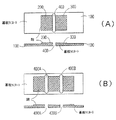
従来のスパークギャップ技術は離散的なスパークギャップ(図1の(A)、(B))又はよりコスト効率の良いプリント回路基板(PCB)スパークギャップ(図2の(A),(B))を含む。離散的なスパークギャップは一般にその間を固定して離間されたそれぞれの導電性表面でガラス、セラミック又はプラスチックの本体内で終端されたリードで形成される。離散的なスパークギャップの2つの範疇があり、1つは図1の(A)に示されるように制御された雰囲気で密封され、他は図1の(B)に示されるように通常の大気で密封されない。これらの型の両方は取付用のかなり大きな空間を必要とし(例えばPCB上に)、両者は離間及び他の機械的な考慮により設けられる間の注意深い物理的な配置及び方向付けが必要である。プリント回路スパークギャップよりコスト的な傾向のある離散的なスパークギャップは幾分より持続的であり、通常より制御された放電電位を示す。 Conventional spark gap technology uses discrete spark gaps (FIGS. 1A and 1B) or more cost-effective printed circuit board (PCB) spark gaps (FIGS. 2A and 2B). Including. Discrete spark gaps are generally formed with leads terminated in a glass, ceramic or plastic body with respective electrically conductive surfaces fixedly spaced therebetween. There are two categories of discrete spark gaps, one sealed in a controlled atmosphere as shown in FIG. 1A and the other in normal atmosphere as shown in FIG. Not sealed with. Both of these types require a significant amount of space for mounting (eg, on a PCB), and both require careful physical placement and orientation while being provided by spacing and other mechanical considerations. Discrete spark gaps, which tend to be more costly than printed circuit spark gaps, are somewhat more durable and exhibit a more controlled discharge potential.
1以上の固定又は柔軟な絶縁体(例えばファイバーグラス又はプラスチック)の層及び1以上の導電材料(例えば銅又は導電性インク)の層からなるプリント回路基板を製造することは良く知られており、ここで種々の回路部品は導電性「トレース」により電気的に接続される。図2(A),(B)に示されるようにPCBスパークギャップは相互に固定された距離で配置され、望まれない過渡現象又は電位の放電用に制御された点を提供するPCBの導電性トレース(例えば銅)を用いる。PCBスパークギャップは電位及び含まれるエネルギーに依存するノード間でラミネートされた基板に穿孔されたスロットを有する。PCBスパークギャップは正確かつ連続的に製造することが比較的容易である。何故ならば物理的な耐性及び配置を通して導入される変化がほとんどないからである。(離散的なスパークギャップと対照的に)PCBスパークギャップは予想可能な動作を提供し、比較的廉価であり、コストは基板材料の実質的なコストよりわずかに高いだけであろう。 It is well known to produce printed circuit boards consisting of one or more layers of fixed or flexible insulator (eg fiberglass or plastic) and one or more layers of conductive material (eg copper or conductive ink), Here, the various circuit components are electrically connected by conductive “traces”. As shown in FIGS. 2A and 2B, PCB spark gaps are placed at fixed distances from each other, and the conductivity of the PCB provides a controlled point for unwanted transients or potential discharges. Use traces (eg copper). PCB spark gaps have slots drilled in a substrate laminated between nodes depending on the potential and energy contained. PCB spark gaps are relatively easy to manufacture accurately and continuously. This is because there is little change introduced through physical tolerance and placement. PCB spark gaps provide predictable operation (as opposed to discrete spark gaps), are relatively inexpensive, and the cost will be only slightly higher than the substantial cost of the substrate material.
プリント回路基板スパークギャップの欠点は繰り返される放電、破局的な事象、又は長期間の一定の放電で明らかである。これらの状況ではプリント回路基板表面及び銅箔は箔の蒸発により導電性ノード間の空間に関して急速に劣化する。ギャップ空間が増加するにつれてギャップを横切るアークに対して必要な電位は増加し、アークの位置はより制御されない。付加的に基板のラミネートはその様な事象を生ずる集中的な熱により破局的かつ長期の放電中の損傷を維持する。 The disadvantages of the printed circuit board spark gap are evident with repeated discharges, catastrophic events, or long-term constant discharges. In these situations, the printed circuit board surface and the copper foil rapidly degrade with respect to the space between the conductive nodes due to the evaporation of the foil. As the gap space increases, the required potential for the arc across the gap increases and the position of the arc is less controlled. Additionally, the substrate laminate maintains damage during catastrophic and long-term discharges due to the concentrated heat that causes such an event.
PCBスパークギャップを改善するのに有用な幾つかの技術がある。例えば箔の蒸発に関する問題は箔の厚さを増加させることにより又はスパークギャップのPCBスロット型で、スロットの長さを増加することにより(その一方で同じ幅を維持する)遅らせることが可能である。しかしながらスパークギャップを実施することを必要とするPCBの領域はこの技術で増加し、蒸発は実質的に性能を劣化する。他の技術はスパークのエネルギーが2つのギャップに亘り散逸するような離間された一連の多数のギャップの使用である(図2の(B))。この技術はまたPCB領域の消費で箔の損傷を遅くする。 There are several techniques that are useful to improve the PCB spark gap. For example, problems with foil evaporation can be delayed by increasing the thickness of the foil or by increasing the slot length (while maintaining the same width) with a spark gap PCB slot type. . However, the area of PCBs that need to perform a spark gap is increased with this technique, and evaporation substantially degrades performance. Another technique is the use of a series of spaced multiple gaps such that the spark energy is dissipated across the two gaps (FIG. 2B). This technique also slows down foil damage with PCB area consumption.
故に本発明の目的は従来技術のスパークギャップの上記制限を減少又は除去するスパークギャップを提供することにある。 Accordingly, it is an object of the present invention to provide a spark gap that reduces or eliminates the above limitations of prior art spark gaps.
本発明は上記のPCBスパークギャップの型の改善に関し、それは相互に先端を突き合わせるよう向けられ、スパークギャップのそれぞれのPCB導電対にはんだ付けされる表面取付デバイス(SMD)を用いる。 The present invention relates to an improvement in the PCB spark gap mold described above, which uses surface mount devices (SMDs) that are oriented to abut each other and soldered to each PCB conductive pair of the spark gap.
本発明は図を参照してより詳細に説明される。種々の図に示される類似の符号は同じ又は類似の要素を示す。図3の(A)及び図5を参照するに、本発明によるPCBスパークギャップの実施例が示される。PCBは非導電性の基板又はラミネート100及びラミネート100上に形成された導体200、300を含む導電性層を含む。導体200、300はスパークギャップ400を形成するよう離間され、相互に電気的に絶縁間される。スパークギャップ400は表面取付デバイス(SMD)210、310の付加により増強され、これは導体200、300にそれぞれはんだ付けされる。示されたギャップ400はラミネート100を通して穿孔されたスロットを含む。しかしながらその様なスロットを穿孔することは本発明の実施に必要ではない。SMD210は導体端230、231ではんだフィレット220、221を介して導体200に電気的、機械的に接続される。SMD310は導体端230、231ではんだフィレット320、321を介して導体300に電気的、機械的に接続される。
The invention is explained in more detail with reference to the figures. Like numbers shown in the various figures indicate the same or similar elements. Referring to FIGS. 3A and 5, an embodiment of a PCB spark gap according to the present invention is shown. The PCB includes a non-conductive substrate or
それを横切ってスパークの形で電気的エネルギーが移動する実際のギャップ400は導体200と300との間の空間により最初に形成される。これらの導体はそれらがギャップがSMD210とSMD310との間で形成されるところで浸食されるようにある蒸気化をなされる。SMDと導体の端との間で導体の量は用いられたSMD処理の取付耐性及びはんだフィレットの構成により決定される。
The
スパークギャップ400の第一の電極は導体200及びはんだフィレット220により形成され、第二の電極は導体300及びはんだフィレット320により形成される。スパークは2つの電極間の電位差がギャップの幅に依存するレベル及び材料の耐電圧(例えばスロットの場合は空気、又はファイバーグラス)を超えたときに1の電極から他へジャンプする。SMD210又は310間の導電性箔ははんだフィレット220、320がこの形へ流れ込むような点に決定されるように設けられるよう形成される。このような方法でアークの位置及び従って引き起こされることが要求される電圧差のレベルがより正確に制御される。この決定された点はより制御しにくい丸い又は広い放電表面と対比して望ましい電位と位置での放電を促進する。
The first electrode of the
第一の電極のみを考えるとアークオーバーにより電極に現れる電気的エネルギーは導体200、はんだフィレット220、SMD210の導体の端230により散逸される。加えて電極の導電性材料内での損失I2 Rにより発生された熱はSMD210及びラミネート100のような隣接した材料に移動する。図2の(A)の従来技術のスパークギャップでは電気的熱的エネルギーは銅及びラミネートのみにより散逸され、上記のような導電体及びラミネートの腐食を生じた。表面取付デバイスを用いることにより及びそれらに関連するはんだフィレット及び導体端により銅から熱を吸収するために用いられる質量は増加し、銅及び隣接するラミネートに対する損傷は最小化される。加えてはんだフィレットにより設けられる大きな断面領域及び導体端はアークオーバー中の電流への抵抗を低くすることによりI2R損失を直接減少し、それにより発生される熱の量を減少する。
Considering only the first electrode, the electrical energy that appears at the electrode due to the arc over is dissipated by the
本発明は図に示されるように又はそれぞれ導体200、300によるSMD210,SMD310の「短絡」なしに実施されうる。しかしながらSMDの下の付加的な銅は電気的な抵抗を低くし、熱質量(即ち損害なしにより多くの熱を吸収する)を増加することの両方により付加的な保護を提供する。熱的な質量の更なる増加は異なるはんだ複合物を用いることにより実現される。例えば特定のはんだ複合物はその高い特徴的な熱特性故に選択される。特定のはんだ複合物はまた特定の流体又は凝固特性により選択され、それにより通常得られない厚いはんだ接合が形成される。
The present invention may be practiced as shown in the figure or without “short circuit” of
用いられたSMDは通常の技術と耐久性を用いてPCBの銅の層にはんだ付けされる。例えばウエーブ又はリフロー方法、蒸気相及び赤外技術である。加えて用いられるSMDの実際の部品の型は上記のようにデバイスが「短絡」されるところで臨界的ではない。デバイスが「短絡」されていないことで部品の選択はより重要であり、低インピーダンス部品(例えばSMDのジャンパー型)が適切な選択である。実際的なこととしてSMD抵抗はSMDコンデンサより機械的に堅固であり、故により望ましいが、両方とも用いられ得る。同様にして選択されたデバイスの耐久性は臨界的ではない。その様な電気的に拒否される部品はそれらが適切な機械的な特性を維持する(例えばかけない等々)場合になお用いられ得る。加えてSMDはスパークギャップで用いるために特別に貯蔵される必要はなく、他の目的で発注されたSMDも用いることが可能である。 The SMD used is soldered to the copper layer of the PCB using conventional techniques and durability. For example, wave or reflow methods, vapor phase and infrared techniques. In addition, the actual component type of the SMD used is not critical where the device is “shorted” as described above. Component selection is more important because the device is not “shorted”, and low impedance components (eg, SMD jumper type) are a good choice. As a practical matter, SMD resistors are mechanically more robust than SMD capacitors and are therefore more desirable, but both can be used. Similarly, the durability of the device selected is not critical. Such electrically rejected parts can still be used if they maintain (e.g. do not apply) proper mechanical properties. In addition, SMDs do not need to be specifically stored for use in the spark gap, and SMDs ordered for other purposes can also be used.
本発明はまた図4の構成を用いて実施でき、ここで2つの対向するSMDはスパークギャップ400を形成するよう用いられる。図4の配置の変形は図3の(A),(B)に示される。図3の(A)は2つの対向するSMDの対からなるスパークギャップ400を有する第二の導体300上に設けられたSMDの第二の対310A,Bに対向する第一の導体200上に設けられたSMDの第一の対210A,Bを示す。この構成はアークオーバーに対する2つの決定された表面があるところにある冗長性を提供する。このような2つの表面を設けることによりスパークギャップの耐久性は増加する。何故ならば対向するSMDの一つの組の表面を決定するどのような顕著な劣化も対向するSMDの他の組の間のアークを実際に生ずるからである。
The present invention can also be implemented using the configuration of FIG. 4, where two opposing SMDs are used to form the
図3の(B)は更なる配列の増強を示す。SMDの第一210A,Bと第二310A,Bの対の間のSMDの第三の対510A,Bは第二のスパークギャップを形成するために設けられている。この配置は2つのギャップ400Aと400Bとの間のアークオーバーエネルギーの分割を許容し、それによりスパークギャップからなるそれぞれの要素上のストレスを減少する。例えば同一のアークオーバー電圧を仮定すると、図3の(A)の配置での単一のスパークギャップは図3の(B)の配置での2つのスパークギャップのいずれよりも広いことが必要とされ、放散される熱的、電気的エネルギーは図3の(A)の配置でのより少ない部品により放散される。故に図3の(B)の配置は関連する部品の劣化を増加することなく図3の(A)の配置より高いエネルギースパークを許容する。
FIG. 3B shows further sequence enhancement. A
また本発明は、図6の配置を用いて実施されても良い。ここで、第一のSMD210A、及び任意の第二のSMD210Bは、第2の導体300と対向する第一の導体200上に設置される。スパークギャップ400は、それに取り付けられている1または2以上のSMDの導電性表面を有する第一の導体と、第二の導体の間にギャップを有する。この実施例では、アークによって生じるスパークギャップの一つの側の損傷が有意に保護されるという、従来技術にはない有意な効果が得られる。
The present invention may also be implemented using the arrangement of FIG. Here, the
従来のPCBスパークギャップと比較したときにコストの増加は最小であり、本質的に2以上のSMD及びそれらのPCB上への配置のコストからなる。加えて図1の(A)の離散的なスパークギャップの代わりとしてのSMDの使用は表面取付技術の恩恵(例えば正確で代替可能な部品配置等々...)という利点を有する。 The cost increase is minimal when compared to a conventional PCB spark gap, consisting essentially of the cost of two or more SMDs and their placement on the PCB. In addition, the use of SMD as an alternative to the discrete spark gap of FIG. 1A has the advantage of surface mounting technology benefits (eg, accurate and replaceable component placement, etc.).
SMD配置は選択された配置/はんだ付け処理の機械的公差及び配置誤差の最悪の場合の組合せがギャップエッジでの部品により覆われていない導体のある量が常に存在することを保証するように選択されるべきである。この配置の目的ははんだ接続と最初の放電開始に対する決められた点の両方を保証することである。 SMD placement selected to ensure that there is always a certain amount of conductor that is not covered by the part at the gap edge with the worst case combination of mechanical tolerances and placement errors of the chosen placement / soldering process It should be. The purpose of this arrangement is to ensure both the solder connection and a fixed point for the first discharge start.
スパークギャップは805又は1206SMD部品のいずれかを用いて構成される。例えば概略O 5ミルのSMD対の端と端の設置精度及び概略100ミルの側面と側面のクリアランスを有する図3の(A)に示されるような発明の実施例上での導電テストはよい結果をもたらす。配置過程のガイドラインはSMDの端を越える銅の20ミルを要求するが、この距離は例えば保護溝のレベルに依存して減少する。 The spark gap is constructed using either 805 or 1206 SMD components. For example, the conductivity test on the embodiment of the invention as shown in FIG. 3A, which has an end-to-end placement accuracy of approximately O 5 mil SMD pair and approximately 100 mil side to side clearance, is a good result. Bring. The placement process guidelines require 20 mils of copper beyond the edge of the SMD, but this distance decreases, for example depending on the level of the protective groove.
SMD取付過程の要因により(例えば隣接部品はんだ付け)、側面と側面の中心線クリアランスは805の大きさのSMDに対して中心線と中心線を90ミルに接近し、1206の大きさのSMDに対して中心線と中心線を100ミルに接近する。5ミルのはんだフィレットを達成するために要求される端のクリアランスはまた充分な電気的、機械的接続を提供する。
Due to factors in the SMD mounting process (for example, soldering of adjacent parts), the centerline clearance between the side and side is close to 90 mil for the SMD size of 805, and the SMD size of 1206 In contrast, the centerline and
上記物理的な寸法を有する図3の(A)の配置でなされた反復的な過渡及びサージを含む実験において、非常に満足できる結果が得られた。ジャンパー型SMDを用いた6KV及び0.51uf毎に20以上のサージからなるテストがなされた。導体は実質的に劣化を被らないことがわかった。図2の(A)の従来技術の配置でなされた同様の実験は銅の顕著な劣化を生じた。本発明のスパークギャップは過渡的な及び連続的な放電デバイスの両方で有用であることが示された。 In experiments involving repetitive transients and surges made in the arrangement of FIG. 3 having the physical dimensions (A), very satisfactory results were obtained. Tests with more than 20 surges were performed every 6 KV and 0.51 uf using a jumper type SMD. It has been found that the conductor is not substantially degraded. Similar experiments made with the prior art arrangement of FIG. 2A resulted in significant degradation of copper. The spark gap of the present invention has been shown to be useful in both transient and continuous discharge devices.
当業者には明らかであるが本発明は特定の例を特に参照して説明されてきたが変更及び改善は本発明の本質から離れることなく開示された実施例に対してなされうる。故に請求項は上記の例から自然に生ずる全ての変更に亘るよう意図されるものである。 Although the present invention has been described with particular reference to specific examples as will be apparent to those skilled in the art, changes and modifications may be made to the disclosed embodiments without departing from the essence of the invention. Thus, the claims are intended to cover all modifications that naturally occur from the above examples.
100 ラミネート
200、300 導体
210、310 表面取付デバイス(SMD)
210A,B、310A,B、510A,B SMD
220、221、320、321 はんだフィレット
230、231 導体端
400 スパークギャップ
210A, B, 310A, B, 510A, B SMD
220, 221, 320, 321
Claims (2)
第一の導電性表面および前記少なくとも2つの第一の表面取付デバイスは、所定の間隔だけ、第二の導電性表面から分離されており、前記第二の導電性表面と協働して、両導電性表面の間に電気的なアークを可能にするギャップを形成し、
前記少なくとも2つの第一の表面取付デバイスは、熱吸収部材であることを特徴とするプリント回路基板スパークギャップ。 Having at least two first surface mounting devices, each disposed on a first conductive surface and having a first flat surface;
The first conductive surface and the at least two first surface mounting devices are separated from the second conductive surface by a predetermined distance, and in cooperation with the second conductive surface, Forming a gap that allows an electrical arc between both conductive surfaces;
The printed circuit board spark gap, wherein the at least two first surface mount devices are heat absorbing members.
Applications Claiming Priority (2)
| Application Number | Priority Date | Filing Date | Title |
|---|---|---|---|
| US08/603,050 US5933307A (en) | 1996-02-16 | 1996-02-16 | Printed circuit board sparkgap |
| US603050 | 1996-02-16 |
Related Parent Applications (1)
| Application Number | Title | Priority Date | Filing Date |
|---|---|---|---|
| JP8348761A Division JPH09232065A (en) | 1996-02-16 | 1996-12-26 | Printed circuit board spark gap |
Publications (2)
| Publication Number | Publication Date |
|---|---|
| JP2008159597A JP2008159597A (en) | 2008-07-10 |
| JP4745357B2 true JP4745357B2 (en) | 2011-08-10 |
Family
ID=24413889
Family Applications (2)
| Application Number | Title | Priority Date | Filing Date |
|---|---|---|---|
| JP8348761A Pending JPH09232065A (en) | 1996-02-16 | 1996-12-26 | Printed circuit board spark gap |
| JP2008052492A Expired - Fee Related JP4745357B2 (en) | 1996-02-16 | 2008-03-03 | Printed circuit board spark gap |
Family Applications Before (1)
| Application Number | Title | Priority Date | Filing Date |
|---|---|---|---|
| JP8348761A Pending JPH09232065A (en) | 1996-02-16 | 1996-12-26 | Printed circuit board spark gap |
Country Status (12)
| Country | Link |
|---|---|
| US (1) | US5933307A (en) |
| EP (1) | EP0790758B1 (en) |
| JP (2) | JPH09232065A (en) |
| KR (1) | KR100441037B1 (en) |
| CN (1) | CN1052347C (en) |
| BR (1) | BR9606195A (en) |
| DE (1) | DE69633848T2 (en) |
| HK (1) | HK1005111A1 (en) |
| ID (1) | ID15938A (en) |
| IN (1) | IN189905B (en) |
| MY (1) | MY120205A (en) |
| SG (1) | SG48504A1 (en) |
Families Citing this family (33)
| Publication number | Priority date | Publication date | Assignee | Title |
|---|---|---|---|---|
| GB2334626B (en) * | 1998-02-20 | 2003-01-29 | Mitel Corp | Spark gap for hermetically packaged integrated circuits |
| GB2335084B (en) | 1998-02-21 | 2003-04-02 | Mitel Corp | Spark gap for high voltage integrated circuit electrostatic discharge protection |
| WO2001017320A1 (en) | 1999-08-27 | 2001-03-08 | Lex Kosowsky | Current carrying structure using voltage switchable dielectric material |
| US7695644B2 (en) | 1999-08-27 | 2010-04-13 | Shocking Technologies, Inc. | Device applications for voltage switchable dielectric material having high aspect ratio particles |
| US7825491B2 (en) | 2005-11-22 | 2010-11-02 | Shocking Technologies, Inc. | Light-emitting device using voltage switchable dielectric material |
| US6493198B1 (en) * | 2000-02-22 | 2002-12-10 | Motorola, Inc. | Electrostatic discharge protection device for a high density printed circuit board |
| CN2478312Y (en) * | 2001-04-10 | 2002-02-20 | 伊博电源(杭州)有限公司 | Surface packed electrical connector |
| US7126804B1 (en) | 2002-07-03 | 2006-10-24 | Diversified Control, Inc. | Spark gap |
| JP4768617B2 (en) * | 2003-10-08 | 2011-09-07 | コンティネンタル・テーベス・アクチエンゲゼルシヤフト・ウント・コンパニー・オッフェネ・ハンデルスゲゼルシヤフト | Embedded microprocessor system for safety limit control. |
| US7885083B2 (en) * | 2003-12-31 | 2011-02-08 | Honeywell International, Inc. | Input transient protection for electronic devices |
| US20060250744A1 (en) * | 2005-05-05 | 2006-11-09 | Mctigue Michael T | Micro gap method and ESD protection device |
| EP1969627A4 (en) | 2005-11-22 | 2010-01-20 | Shocking Technologies Inc | Semiconductor devices including voltage switchable materials for over-voltage protection |
| US7968014B2 (en) | 2006-07-29 | 2011-06-28 | Shocking Technologies, Inc. | Device applications for voltage switchable dielectric material having high aspect ratio particles |
| WO2008036423A2 (en) | 2006-09-24 | 2008-03-27 | Shocking Technologies, Inc. | Formulations for voltage switchable dielectric material having a stepped voltage response and methods for making the same |
| US7793236B2 (en) | 2007-06-13 | 2010-09-07 | Shocking Technologies, Inc. | System and method for including protective voltage switchable dielectric material in the design or simulation of substrate devices |
| US8112884B2 (en) | 2007-10-08 | 2012-02-14 | Honeywell International Inc. | Method for providing an efficient thermal transfer through a printed circuit board |
| GB2453765A (en) | 2007-10-18 | 2009-04-22 | Novalia Ltd | Product packaging with printed circuit and means for preventing a short circuit |
| US8203421B2 (en) | 2008-04-14 | 2012-06-19 | Shocking Technologies, Inc. | Substrate device or package using embedded layer of voltage switchable dielectric material in a vertical switching configuration |
| US9208931B2 (en) | 2008-09-30 | 2015-12-08 | Littelfuse, Inc. | Voltage switchable dielectric material containing conductor-on-conductor core shelled particles |
| CN102246246A (en) | 2008-09-30 | 2011-11-16 | 肖克科技有限公司 | Voltage switchable dielectric material containing conductive core shelled particles |
| US8399773B2 (en) | 2009-01-27 | 2013-03-19 | Shocking Technologies, Inc. | Substrates having voltage switchable dielectric materials |
| US8272123B2 (en) | 2009-01-27 | 2012-09-25 | Shocking Technologies, Inc. | Substrates having voltage switchable dielectric materials |
| KR101679099B1 (en) | 2009-03-26 | 2016-11-23 | 쇼킹 테크놀로지스 인코포레이티드 | Components having voltage switchable dielectric materials |
| US9053844B2 (en) | 2009-09-09 | 2015-06-09 | Littelfuse, Inc. | Geometric configuration or alignment of protective material in a gap structure for electrical devices |
| US9224728B2 (en) | 2010-02-26 | 2015-12-29 | Littelfuse, Inc. | Embedded protection against spurious electrical events |
| US9320135B2 (en) | 2010-02-26 | 2016-04-19 | Littelfuse, Inc. | Electric discharge protection for surface mounted and embedded components |
| US9082622B2 (en) | 2010-02-26 | 2015-07-14 | Littelfuse, Inc. | Circuit elements comprising ferroic materials |
| US8395875B2 (en) | 2010-08-13 | 2013-03-12 | Andrew F. Tresness | Spark gap apparatus |
| US10064266B2 (en) | 2011-07-19 | 2018-08-28 | Whirlpool Corporation | Circuit board having arc tracking protection |
| US11311225B2 (en) * | 2017-07-11 | 2022-04-26 | General Electric Company | Systems and methods for shielded and adjustable medical monitoring devices |
| JP2019117852A (en) * | 2017-12-27 | 2019-07-18 | パナソニックIpマネジメント株式会社 | Printed circuit board and ceiling fan |
| CN108923262B (en) * | 2018-06-28 | 2020-09-15 | 新华三技术有限公司 | Spark discharger, circuit board, and electronic device |
| EP3906378B1 (en) * | 2019-01-03 | 2022-05-18 | Signify Holding B.V. | Apparatus with charge dissipation |
Family Cites Families (10)
| Publication number | Priority date | Publication date | Assignee | Title |
|---|---|---|---|---|
| FR2326107A1 (en) * | 1974-05-13 | 1977-04-22 | Seiko Instr & Electronics | PRINTED CIRCUIT PANEL |
| JPS5231376A (en) * | 1975-09-05 | 1977-03-09 | Hitachi Ltd | Discharge electrode at thick printed circuit substrate |
| JPS54148861A (en) * | 1978-05-16 | 1979-11-21 | Naoyoshi Adachi | Parison for hollow mold articles and production thereof |
| JPS55126983A (en) * | 1979-03-26 | 1980-10-01 | Hitachi Ltd | Discharge gap |
| JPS57143692A (en) * | 1981-02-28 | 1982-09-04 | Matsushita Electric Works Ltd | Call chime system |
| DE3271524D1 (en) * | 1982-03-25 | 1986-07-10 | Ibm Deutschland | Transistor circuit for switching the printing current in a metal paper printer and for automatically reducing the printing current after spark ignition |
| JPH07107867B2 (en) * | 1986-05-27 | 1995-11-15 | 三菱マテリアル株式会社 | Multi-pole micro gap type surge absorber |
| JPH04239114A (en) * | 1991-01-11 | 1992-08-27 | Toyota Motor Corp | Surface mounted type electronic part |
| CA2103510A1 (en) * | 1992-09-11 | 1994-03-12 | Bradley D. Harris | Printed circuit bridge for an airbag inflator |
| DE4329251C2 (en) * | 1993-08-31 | 1996-08-14 | Philips Patentverwaltung | Arrangement for protecting components sensitive to overvoltages on printed circuit boards |
-
1996
- 1996-02-16 US US08/603,050 patent/US5933307A/en not_active Expired - Lifetime
- 1996-12-06 EP EP96119610A patent/EP0790758B1/en not_active Expired - Lifetime
- 1996-12-06 DE DE69633848T patent/DE69633848T2/en not_active Expired - Lifetime
- 1996-12-09 IN IN2120CA1996 patent/IN189905B/en unknown
- 1996-12-11 SG SG1996011952A patent/SG48504A1/en unknown
- 1996-12-17 CN CN96121363A patent/CN1052347C/en not_active Expired - Fee Related
- 1996-12-26 JP JP8348761A patent/JPH09232065A/en active Pending
- 1996-12-27 BR BR9606195A patent/BR9606195A/en not_active IP Right Cessation
- 1996-12-27 KR KR1019960072708A patent/KR100441037B1/en not_active IP Right Cessation
-
1997
- 1997-01-03 MY MYPI97000011A patent/MY120205A/en unknown
- 1997-02-14 ID IDP970424A patent/ID15938A/en unknown
-
1998
- 1998-05-18 HK HK98104264A patent/HK1005111A1/en not_active IP Right Cessation
-
2008
- 2008-03-03 JP JP2008052492A patent/JP4745357B2/en not_active Expired - Fee Related
Also Published As
| Publication number | Publication date |
|---|---|
| CN1165419A (en) | 1997-11-19 |
| ID15938A (en) | 1997-08-21 |
| KR100441037B1 (en) | 2004-10-26 |
| KR970064340A (en) | 1997-09-12 |
| JP2008159597A (en) | 2008-07-10 |
| EP0790758A1 (en) | 1997-08-20 |
| BR9606195A (en) | 1998-08-18 |
| MY120205A (en) | 2005-09-30 |
| IN189905B (en) | 2003-05-10 |
| JPH09232065A (en) | 1997-09-05 |
| EP0790758B1 (en) | 2004-11-17 |
| HK1005111A1 (en) | 1998-12-24 |
| DE69633848D1 (en) | 2004-12-23 |
| DE69633848T2 (en) | 2005-03-31 |
| US5933307A (en) | 1999-08-03 |
| SG48504A1 (en) | 1998-04-17 |
| CN1052347C (en) | 2000-05-10 |
Similar Documents
| Publication | Publication Date | Title |
|---|---|---|
| JP4745357B2 (en) | Printed circuit board spark gap | |
| US7218492B2 (en) | Devices and systems for electrostatic discharge suppression | |
| US20060152334A1 (en) | Electrostatic discharge protection for embedded components | |
| US5493259A (en) | High voltage, low pass filtering connector with multiple ground planes | |
| US20050185356A1 (en) | Overvoltage protection element and ignition element for an overvoltage protection element | |
| US6430017B1 (en) | Thermal protection for surge suppressors | |
| US20120039010A1 (en) | Spark Gap Apparatus | |
| EP1835578A1 (en) | Lightning arrester | |
| US5083237A (en) | Electronic parts and electronic device incorporating the same | |
| MXPA96006645A (en) | Disruptive distance from circuit board | |
| US6995984B2 (en) | Method for producing a large-mass ohmic resistor for protecting electronic assemblies from surges, and an electronic assembly | |
| GB1143208A (en) | Electronic component | |
| JP3536592B2 (en) | Discharge tube type surge absorber | |
| KR960016777B1 (en) | Surge absorber of gap type | |
| US5576922A (en) | Surge absorbing structure, surge absorbing element, connector and circuit device using these structure and element | |
| JP3136760B2 (en) | Chip type three-terminal capacitor | |
| US5244416A (en) | Multicontact connector protected against interference | |
| EP1090399B1 (en) | Surge protector | |
| JP2963420B2 (en) | Square chip electronic components | |
| JPH027482Y2 (en) | ||
| KR20170075423A (en) | Resistor element and board having the same mounted thereon | |
| JPH04277479A (en) | Lightning arrester | |
| JPS6224588A (en) | Surge protector | |
| JPH07162123A (en) | Circuit module | |
| JPH11233231A (en) | Abnormal voltage protector |
Legal Events
| Date | Code | Title | Description |
|---|---|---|---|
| A131 | Notification of reasons for refusal |
Free format text: JAPANESE INTERMEDIATE CODE: A131 Effective date: 20100914 |
|
| A601 | Written request for extension of time |
Free format text: JAPANESE INTERMEDIATE CODE: A601 Effective date: 20101209 |
|
| A602 | Written permission of extension of time |
Free format text: JAPANESE INTERMEDIATE CODE: A602 Effective date: 20101214 |
|
| A521 | Written amendment |
Free format text: JAPANESE INTERMEDIATE CODE: A523 Effective date: 20110314 |
|
| A01 | Written decision to grant a patent or to grant a registration (utility model) |
Free format text: JAPANESE INTERMEDIATE CODE: A01 Effective date: 20110419 |
|
| A01 | Written decision to grant a patent or to grant a registration (utility model) |
Free format text: JAPANESE INTERMEDIATE CODE: A01 |
|
| A61 | First payment of annual fees (during grant procedure) |
Free format text: JAPANESE INTERMEDIATE CODE: A61 Effective date: 20110511 |
|
| FPAY | Renewal fee payment (event date is renewal date of database) |
Free format text: PAYMENT UNTIL: 20140520 Year of fee payment: 3 |
|
| R150 | Certificate of patent or registration of utility model |
Free format text: JAPANESE INTERMEDIATE CODE: R150 |
|
| LAPS | Cancellation because of no payment of annual fees |