JP4653659B2 - Driving method of self-luminous display device - Google Patents
Driving method of self-luminous display device Download PDFInfo
- Publication number
- JP4653659B2 JP4653659B2 JP2005512611A JP2005512611A JP4653659B2 JP 4653659 B2 JP4653659 B2 JP 4653659B2 JP 2005512611 A JP2005512611 A JP 2005512611A JP 2005512611 A JP2005512611 A JP 2005512611A JP 4653659 B2 JP4653659 B2 JP 4653659B2
- Authority
- JP
- Japan
- Prior art keywords
- current
- value
- data
- transistor
- display
- Prior art date
- Legal status (The legal status is an assumption and is not a legal conclusion. Google has not performed a legal analysis and makes no representation as to the accuracy of the status listed.)
- Active
Links
- 238000000034 method Methods 0.000 title claims description 214
- 230000008859 change Effects 0.000 claims description 66
- 230000008569 process Effects 0.000 claims description 23
- 239000011159 matrix material Substances 0.000 claims description 22
- 238000012545 processing Methods 0.000 claims description 19
- 238000005401 electroluminescence Methods 0.000 description 205
- 238000010586 diagram Methods 0.000 description 125
- 230000001276 controlling effect Effects 0.000 description 69
- 238000003780 insertion Methods 0.000 description 59
- 230000037431 insertion Effects 0.000 description 59
- 230000002829 reductive effect Effects 0.000 description 47
- 239000003990 capacitor Substances 0.000 description 39
- 239000010408 film Substances 0.000 description 32
- 230000000875 corresponding effect Effects 0.000 description 26
- 230000006866 deterioration Effects 0.000 description 26
- 230000001629 suppression Effects 0.000 description 26
- 238000003860 storage Methods 0.000 description 18
- 230000000694 effects Effects 0.000 description 16
- 230000015556 catabolic process Effects 0.000 description 14
- 230000006870 function Effects 0.000 description 14
- 239000004973 liquid crystal related substance Substances 0.000 description 14
- 238000006243 chemical reaction Methods 0.000 description 13
- 230000007423 decrease Effects 0.000 description 13
- 238000006731 degradation reaction Methods 0.000 description 13
- 238000005516 engineering process Methods 0.000 description 13
- 230000008901 benefit Effects 0.000 description 12
- 239000010410 layer Substances 0.000 description 12
- 230000001681 protective effect Effects 0.000 description 12
- 238000004364 calculation method Methods 0.000 description 11
- 239000000758 substrate Substances 0.000 description 11
- 238000009826 distribution Methods 0.000 description 10
- 230000007246 mechanism Effects 0.000 description 9
- 229910021420 polycrystalline silicon Inorganic materials 0.000 description 9
- 229910021417 amorphous silicon Inorganic materials 0.000 description 8
- 239000000463 material Substances 0.000 description 8
- 239000002184 metal Substances 0.000 description 8
- 229910052751 metal Inorganic materials 0.000 description 8
- 229920005591 polysilicon Polymers 0.000 description 8
- 230000003247 decreasing effect Effects 0.000 description 7
- 230000008878 coupling Effects 0.000 description 6
- 238000010168 coupling process Methods 0.000 description 6
- 238000005859 coupling reaction Methods 0.000 description 6
- 238000004519 manufacturing process Methods 0.000 description 6
- 230000002093 peripheral effect Effects 0.000 description 6
- 238000013461 design Methods 0.000 description 5
- 239000010409 thin film Substances 0.000 description 5
- 230000009471 action Effects 0.000 description 4
- 239000011521 glass Substances 0.000 description 4
- 239000012071 phase Substances 0.000 description 4
- 238000007789 sealing Methods 0.000 description 4
- LYCAIKOWRPUZTN-UHFFFAOYSA-N Ethylene glycol Chemical compound OCCO LYCAIKOWRPUZTN-UHFFFAOYSA-N 0.000 description 3
- 230000005540 biological transmission Effects 0.000 description 3
- 238000000605 extraction Methods 0.000 description 3
- 239000002346 layers by function Substances 0.000 description 3
- 230000009467 reduction Effects 0.000 description 3
- 239000011347 resin Substances 0.000 description 3
- 229920005989 resin Polymers 0.000 description 3
- 239000004065 semiconductor Substances 0.000 description 3
- 101150062589 PTGS1 gene Proteins 0.000 description 2
- 101150000187 PTGS2 gene Proteins 0.000 description 2
- NIXOWILDQLNWCW-UHFFFAOYSA-N acrylic acid group Chemical group C(C=C)(=O)O NIXOWILDQLNWCW-UHFFFAOYSA-N 0.000 description 2
- 239000011230 binding agent Substances 0.000 description 2
- 230000015572 biosynthetic process Effects 0.000 description 2
- 238000005282 brightening Methods 0.000 description 2
- 239000011248 coating agent Substances 0.000 description 2
- 238000000576 coating method Methods 0.000 description 2
- 239000003086 colorant Substances 0.000 description 2
- 238000001514 detection method Methods 0.000 description 2
- 239000003822 epoxy resin Substances 0.000 description 2
- 230000006872 improvement Effects 0.000 description 2
- 238000009413 insulation Methods 0.000 description 2
- 230000003287 optical effect Effects 0.000 description 2
- 230000003071 parasitic effect Effects 0.000 description 2
- 229920000647 polyepoxide Polymers 0.000 description 2
- 239000004925 Acrylic resin Substances 0.000 description 1
- 229920000178 Acrylic resin Polymers 0.000 description 1
- 241001270131 Agaricus moelleri Species 0.000 description 1
- 102100040844 Dual specificity protein kinase CLK2 Human genes 0.000 description 1
- LFQSCWFLJHTTHZ-UHFFFAOYSA-N Ethanol Chemical compound CCO LFQSCWFLJHTTHZ-UHFFFAOYSA-N 0.000 description 1
- PXGOKWXKJXAPGV-UHFFFAOYSA-N Fluorine Chemical compound FF PXGOKWXKJXAPGV-UHFFFAOYSA-N 0.000 description 1
- 101000749291 Homo sapiens Dual specificity protein kinase CLK2 Proteins 0.000 description 1
- 239000004743 Polypropylene Substances 0.000 description 1
- 230000004931 aggregating effect Effects 0.000 description 1
- 238000013459 approach Methods 0.000 description 1
- 239000011324 bead Substances 0.000 description 1
- 230000002457 bidirectional effect Effects 0.000 description 1
- 230000004397 blinking Effects 0.000 description 1
- 238000012937 correction Methods 0.000 description 1
- 230000002596 correlated effect Effects 0.000 description 1
- 239000013078 crystal Substances 0.000 description 1
- 239000002274 desiccant Substances 0.000 description 1
- 239000003599 detergent Substances 0.000 description 1
- 238000011161 development Methods 0.000 description 1
- 238000006073 displacement reaction Methods 0.000 description 1
- 238000011156 evaluation Methods 0.000 description 1
- 230000005669 field effect Effects 0.000 description 1
- 238000001914 filtration Methods 0.000 description 1
- 238000007667 floating Methods 0.000 description 1
- 229910052731 fluorine Inorganic materials 0.000 description 1
- 239000011737 fluorine Substances 0.000 description 1
- 230000003760 hair shine Effects 0.000 description 1
- 230000017525 heat dissipation Effects 0.000 description 1
- 230000020169 heat generation Effects 0.000 description 1
- 230000005525 hole transport Effects 0.000 description 1
- 238000003384 imaging method Methods 0.000 description 1
- 239000012535 impurity Substances 0.000 description 1
- 238000002347 injection Methods 0.000 description 1
- 239000007924 injection Substances 0.000 description 1
- 229910010272 inorganic material Inorganic materials 0.000 description 1
- 239000011147 inorganic material Substances 0.000 description 1
- 238000012966 insertion method Methods 0.000 description 1
- 238000007689 inspection Methods 0.000 description 1
- 239000011229 interlayer Substances 0.000 description 1
- 238000005224 laser annealing Methods 0.000 description 1
- WABPQHHGFIMREM-UHFFFAOYSA-N lead(0) Chemical compound [Pb] WABPQHHGFIMREM-UHFFFAOYSA-N 0.000 description 1
- 239000007788 liquid Substances 0.000 description 1
- 238000004020 luminiscence type Methods 0.000 description 1
- 239000000696 magnetic material Substances 0.000 description 1
- 239000003550 marker Substances 0.000 description 1
- 238000005259 measurement Methods 0.000 description 1
- 150000002894 organic compounds Chemical class 0.000 description 1
- 230000036961 partial effect Effects 0.000 description 1
- 239000005011 phenolic resin Substances 0.000 description 1
- 238000000206 photolithography Methods 0.000 description 1
- 229920006289 polycarbonate film Polymers 0.000 description 1
- 229920006267 polyester film Polymers 0.000 description 1
- -1 polypropylene Polymers 0.000 description 1
- 229920001155 polypropylene Polymers 0.000 description 1
- 238000003825 pressing Methods 0.000 description 1
- 230000002265 prevention Effects 0.000 description 1
- 238000003672 processing method Methods 0.000 description 1
- 230000002040 relaxant effect Effects 0.000 description 1
- 230000004044 response Effects 0.000 description 1
- 230000000717 retained effect Effects 0.000 description 1
- 238000004904 shortening Methods 0.000 description 1
- 239000007787 solid Substances 0.000 description 1
- 239000007790 solid phase Substances 0.000 description 1
- 230000007480 spreading Effects 0.000 description 1
- 238000003892 spreading Methods 0.000 description 1
- 230000000087 stabilizing effect Effects 0.000 description 1
- 239000000126 substance Substances 0.000 description 1
- 239000005341 toughened glass Substances 0.000 description 1
- 230000007704 transition Effects 0.000 description 1
- 238000002834 transmittance Methods 0.000 description 1
- 238000007740 vapor deposition Methods 0.000 description 1
Images


Classifications
-
- G—PHYSICS
- G09—EDUCATION; CRYPTOGRAPHY; DISPLAY; ADVERTISING; SEALS
- G09G—ARRANGEMENTS OR CIRCUITS FOR CONTROL OF INDICATING DEVICES USING STATIC MEANS TO PRESENT VARIABLE INFORMATION
- G09G3/00—Control arrangements or circuits, of interest only in connection with visual indicators other than cathode-ray tubes
- G09G3/20—Control arrangements or circuits, of interest only in connection with visual indicators other than cathode-ray tubes for presentation of an assembly of a number of characters, e.g. a page, by composing the assembly by combination of individual elements arranged in a matrix no fixed position being assigned to or needed to be assigned to the individual characters or partial characters
- G09G3/22—Control arrangements or circuits, of interest only in connection with visual indicators other than cathode-ray tubes for presentation of an assembly of a number of characters, e.g. a page, by composing the assembly by combination of individual elements arranged in a matrix no fixed position being assigned to or needed to be assigned to the individual characters or partial characters using controlled light sources
- G09G3/30—Control arrangements or circuits, of interest only in connection with visual indicators other than cathode-ray tubes for presentation of an assembly of a number of characters, e.g. a page, by composing the assembly by combination of individual elements arranged in a matrix no fixed position being assigned to or needed to be assigned to the individual characters or partial characters using controlled light sources using electroluminescent panels
- G09G3/32—Control arrangements or circuits, of interest only in connection with visual indicators other than cathode-ray tubes for presentation of an assembly of a number of characters, e.g. a page, by composing the assembly by combination of individual elements arranged in a matrix no fixed position being assigned to or needed to be assigned to the individual characters or partial characters using controlled light sources using electroluminescent panels semiconductive, e.g. using light-emitting diodes [LED]
- G09G3/3208—Control arrangements or circuits, of interest only in connection with visual indicators other than cathode-ray tubes for presentation of an assembly of a number of characters, e.g. a page, by composing the assembly by combination of individual elements arranged in a matrix no fixed position being assigned to or needed to be assigned to the individual characters or partial characters using controlled light sources using electroluminescent panels semiconductive, e.g. using light-emitting diodes [LED] organic, e.g. using organic light-emitting diodes [OLED]
- G09G3/3225—Control arrangements or circuits, of interest only in connection with visual indicators other than cathode-ray tubes for presentation of an assembly of a number of characters, e.g. a page, by composing the assembly by combination of individual elements arranged in a matrix no fixed position being assigned to or needed to be assigned to the individual characters or partial characters using controlled light sources using electroluminescent panels semiconductive, e.g. using light-emitting diodes [LED] organic, e.g. using organic light-emitting diodes [OLED] using an active matrix
- G09G3/3233—Control arrangements or circuits, of interest only in connection with visual indicators other than cathode-ray tubes for presentation of an assembly of a number of characters, e.g. a page, by composing the assembly by combination of individual elements arranged in a matrix no fixed position being assigned to or needed to be assigned to the individual characters or partial characters using controlled light sources using electroluminescent panels semiconductive, e.g. using light-emitting diodes [LED] organic, e.g. using organic light-emitting diodes [OLED] using an active matrix with pixel circuitry controlling the current through the light-emitting element
-
- G—PHYSICS
- G09—EDUCATION; CRYPTOGRAPHY; DISPLAY; ADVERTISING; SEALS
- G09G—ARRANGEMENTS OR CIRCUITS FOR CONTROL OF INDICATING DEVICES USING STATIC MEANS TO PRESENT VARIABLE INFORMATION
- G09G3/00—Control arrangements or circuits, of interest only in connection with visual indicators other than cathode-ray tubes
- G09G3/20—Control arrangements or circuits, of interest only in connection with visual indicators other than cathode-ray tubes for presentation of an assembly of a number of characters, e.g. a page, by composing the assembly by combination of individual elements arranged in a matrix no fixed position being assigned to or needed to be assigned to the individual characters or partial characters
- G09G3/22—Control arrangements or circuits, of interest only in connection with visual indicators other than cathode-ray tubes for presentation of an assembly of a number of characters, e.g. a page, by composing the assembly by combination of individual elements arranged in a matrix no fixed position being assigned to or needed to be assigned to the individual characters or partial characters using controlled light sources
- G09G3/30—Control arrangements or circuits, of interest only in connection with visual indicators other than cathode-ray tubes for presentation of an assembly of a number of characters, e.g. a page, by composing the assembly by combination of individual elements arranged in a matrix no fixed position being assigned to or needed to be assigned to the individual characters or partial characters using controlled light sources using electroluminescent panels
- G09G3/32—Control arrangements or circuits, of interest only in connection with visual indicators other than cathode-ray tubes for presentation of an assembly of a number of characters, e.g. a page, by composing the assembly by combination of individual elements arranged in a matrix no fixed position being assigned to or needed to be assigned to the individual characters or partial characters using controlled light sources using electroluminescent panels semiconductive, e.g. using light-emitting diodes [LED]
-
- H—ELECTRICITY
- H05—ELECTRIC TECHNIQUES NOT OTHERWISE PROVIDED FOR
- H05B—ELECTRIC HEATING; ELECTRIC LIGHT SOURCES NOT OTHERWISE PROVIDED FOR; CIRCUIT ARRANGEMENTS FOR ELECTRIC LIGHT SOURCES, IN GENERAL
- H05B33/00—Electroluminescent light sources
- H05B33/12—Light sources with substantially two-dimensional radiating surfaces
-
- G—PHYSICS
- G09—EDUCATION; CRYPTOGRAPHY; DISPLAY; ADVERTISING; SEALS
- G09G—ARRANGEMENTS OR CIRCUITS FOR CONTROL OF INDICATING DEVICES USING STATIC MEANS TO PRESENT VARIABLE INFORMATION
- G09G2300/00—Aspects of the constitution of display devices
- G09G2300/04—Structural and physical details of display devices
- G09G2300/0421—Structural details of the set of electrodes
- G09G2300/0426—Layout of electrodes and connections
-
- G—PHYSICS
- G09—EDUCATION; CRYPTOGRAPHY; DISPLAY; ADVERTISING; SEALS
- G09G—ARRANGEMENTS OR CIRCUITS FOR CONTROL OF INDICATING DEVICES USING STATIC MEANS TO PRESENT VARIABLE INFORMATION
- G09G2300/00—Aspects of the constitution of display devices
- G09G2300/04—Structural and physical details of display devices
- G09G2300/0439—Pixel structures
-
- G—PHYSICS
- G09—EDUCATION; CRYPTOGRAPHY; DISPLAY; ADVERTISING; SEALS
- G09G—ARRANGEMENTS OR CIRCUITS FOR CONTROL OF INDICATING DEVICES USING STATIC MEANS TO PRESENT VARIABLE INFORMATION
- G09G2300/00—Aspects of the constitution of display devices
- G09G2300/08—Active matrix structure, i.e. with use of active elements, inclusive of non-linear two terminal elements, in the pixels together with light emitting or modulating elements
- G09G2300/0809—Several active elements per pixel in active matrix panels
- G09G2300/0814—Several active elements per pixel in active matrix panels used for selection purposes, e.g. logical AND for partial update
-
- G—PHYSICS
- G09—EDUCATION; CRYPTOGRAPHY; DISPLAY; ADVERTISING; SEALS
- G09G—ARRANGEMENTS OR CIRCUITS FOR CONTROL OF INDICATING DEVICES USING STATIC MEANS TO PRESENT VARIABLE INFORMATION
- G09G2300/00—Aspects of the constitution of display devices
- G09G2300/08—Active matrix structure, i.e. with use of active elements, inclusive of non-linear two terminal elements, in the pixels together with light emitting or modulating elements
- G09G2300/0809—Several active elements per pixel in active matrix panels
- G09G2300/0819—Several active elements per pixel in active matrix panels used for counteracting undesired variations, e.g. feedback or autozeroing
-
- G—PHYSICS
- G09—EDUCATION; CRYPTOGRAPHY; DISPLAY; ADVERTISING; SEALS
- G09G—ARRANGEMENTS OR CIRCUITS FOR CONTROL OF INDICATING DEVICES USING STATIC MEANS TO PRESENT VARIABLE INFORMATION
- G09G2300/00—Aspects of the constitution of display devices
- G09G2300/08—Active matrix structure, i.e. with use of active elements, inclusive of non-linear two terminal elements, in the pixels together with light emitting or modulating elements
- G09G2300/0809—Several active elements per pixel in active matrix panels
- G09G2300/0842—Several active elements per pixel in active matrix panels forming a memory circuit, e.g. a dynamic memory with one capacitor
- G09G2300/0861—Several active elements per pixel in active matrix panels forming a memory circuit, e.g. a dynamic memory with one capacitor with additional control of the display period without amending the charge stored in a pixel memory, e.g. by means of additional select electrodes
-
- G—PHYSICS
- G09—EDUCATION; CRYPTOGRAPHY; DISPLAY; ADVERTISING; SEALS
- G09G—ARRANGEMENTS OR CIRCUITS FOR CONTROL OF INDICATING DEVICES USING STATIC MEANS TO PRESENT VARIABLE INFORMATION
- G09G2310/00—Command of the display device
- G09G2310/02—Addressing, scanning or driving the display screen or processing steps related thereto
- G09G2310/0243—Details of the generation of driving signals
- G09G2310/0248—Precharge or discharge of column electrodes before or after applying exact column voltages
-
- G—PHYSICS
- G09—EDUCATION; CRYPTOGRAPHY; DISPLAY; ADVERTISING; SEALS
- G09G—ARRANGEMENTS OR CIRCUITS FOR CONTROL OF INDICATING DEVICES USING STATIC MEANS TO PRESENT VARIABLE INFORMATION
- G09G2310/00—Command of the display device
- G09G2310/02—Addressing, scanning or driving the display screen or processing steps related thereto
- G09G2310/0262—The addressing of the pixel, in a display other than an active matrix LCD, involving the control of two or more scan electrodes or two or more data electrodes, e.g. pixel voltage dependent on signals of two data electrodes
-
- G—PHYSICS
- G09—EDUCATION; CRYPTOGRAPHY; DISPLAY; ADVERTISING; SEALS
- G09G—ARRANGEMENTS OR CIRCUITS FOR CONTROL OF INDICATING DEVICES USING STATIC MEANS TO PRESENT VARIABLE INFORMATION
- G09G2310/00—Command of the display device
- G09G2310/06—Details of flat display driving waveforms
- G09G2310/061—Details of flat display driving waveforms for resetting or blanking
- G09G2310/062—Waveforms for resetting a plurality of scan lines at a time
-
- G—PHYSICS
- G09—EDUCATION; CRYPTOGRAPHY; DISPLAY; ADVERTISING; SEALS
- G09G—ARRANGEMENTS OR CIRCUITS FOR CONTROL OF INDICATING DEVICES USING STATIC MEANS TO PRESENT VARIABLE INFORMATION
- G09G2320/00—Control of display operating conditions
- G09G2320/02—Improving the quality of display appearance
- G09G2320/0209—Crosstalk reduction, i.e. to reduce direct or indirect influences of signals directed to a certain pixel of the displayed image on other pixels of said image, inclusive of influences affecting pixels in different frames or fields or sub-images which constitute a same image, e.g. left and right images of a stereoscopic display
-
- G—PHYSICS
- G09—EDUCATION; CRYPTOGRAPHY; DISPLAY; ADVERTISING; SEALS
- G09G—ARRANGEMENTS OR CIRCUITS FOR CONTROL OF INDICATING DEVICES USING STATIC MEANS TO PRESENT VARIABLE INFORMATION
- G09G2320/00—Control of display operating conditions
- G09G2320/02—Improving the quality of display appearance
- G09G2320/0233—Improving the luminance or brightness uniformity across the screen
-
- G—PHYSICS
- G09—EDUCATION; CRYPTOGRAPHY; DISPLAY; ADVERTISING; SEALS
- G09G—ARRANGEMENTS OR CIRCUITS FOR CONTROL OF INDICATING DEVICES USING STATIC MEANS TO PRESENT VARIABLE INFORMATION
- G09G2320/00—Control of display operating conditions
- G09G2320/02—Improving the quality of display appearance
- G09G2320/0238—Improving the black level
-
- G—PHYSICS
- G09—EDUCATION; CRYPTOGRAPHY; DISPLAY; ADVERTISING; SEALS
- G09G—ARRANGEMENTS OR CIRCUITS FOR CONTROL OF INDICATING DEVICES USING STATIC MEANS TO PRESENT VARIABLE INFORMATION
- G09G2320/00—Control of display operating conditions
- G09G2320/02—Improving the quality of display appearance
- G09G2320/0247—Flicker reduction other than flicker reduction circuits used for single beam cathode-ray tubes
-
- G—PHYSICS
- G09—EDUCATION; CRYPTOGRAPHY; DISPLAY; ADVERTISING; SEALS
- G09G—ARRANGEMENTS OR CIRCUITS FOR CONTROL OF INDICATING DEVICES USING STATIC MEANS TO PRESENT VARIABLE INFORMATION
- G09G2320/00—Control of display operating conditions
- G09G2320/02—Improving the quality of display appearance
- G09G2320/0261—Improving the quality of display appearance in the context of movement of objects on the screen or movement of the observer relative to the screen
-
- G—PHYSICS
- G09—EDUCATION; CRYPTOGRAPHY; DISPLAY; ADVERTISING; SEALS
- G09G—ARRANGEMENTS OR CIRCUITS FOR CONTROL OF INDICATING DEVICES USING STATIC MEANS TO PRESENT VARIABLE INFORMATION
- G09G2320/00—Control of display operating conditions
- G09G2320/02—Improving the quality of display appearance
- G09G2320/0271—Adjustment of the gradation levels within the range of the gradation scale, e.g. by redistribution or clipping
-
- G—PHYSICS
- G09—EDUCATION; CRYPTOGRAPHY; DISPLAY; ADVERTISING; SEALS
- G09G—ARRANGEMENTS OR CIRCUITS FOR CONTROL OF INDICATING DEVICES USING STATIC MEANS TO PRESENT VARIABLE INFORMATION
- G09G2320/00—Control of display operating conditions
- G09G2320/04—Maintaining the quality of display appearance
- G09G2320/041—Temperature compensation
-
- G—PHYSICS
- G09—EDUCATION; CRYPTOGRAPHY; DISPLAY; ADVERTISING; SEALS
- G09G—ARRANGEMENTS OR CIRCUITS FOR CONTROL OF INDICATING DEVICES USING STATIC MEANS TO PRESENT VARIABLE INFORMATION
- G09G2320/00—Control of display operating conditions
- G09G2320/04—Maintaining the quality of display appearance
- G09G2320/043—Preventing or counteracting the effects of ageing
- G09G2320/045—Compensation of drifts in the characteristics of light emitting or modulating elements
-
- G—PHYSICS
- G09—EDUCATION; CRYPTOGRAPHY; DISPLAY; ADVERTISING; SEALS
- G09G—ARRANGEMENTS OR CIRCUITS FOR CONTROL OF INDICATING DEVICES USING STATIC MEANS TO PRESENT VARIABLE INFORMATION
- G09G2320/00—Control of display operating conditions
- G09G2320/04—Maintaining the quality of display appearance
- G09G2320/043—Preventing or counteracting the effects of ageing
- G09G2320/046—Dealing with screen burn-in prevention or compensation of the effects thereof
-
- G—PHYSICS
- G09—EDUCATION; CRYPTOGRAPHY; DISPLAY; ADVERTISING; SEALS
- G09G—ARRANGEMENTS OR CIRCUITS FOR CONTROL OF INDICATING DEVICES USING STATIC MEANS TO PRESENT VARIABLE INFORMATION
- G09G2320/00—Control of display operating conditions
- G09G2320/06—Adjustment of display parameters
- G09G2320/0626—Adjustment of display parameters for control of overall brightness
-
- G—PHYSICS
- G09—EDUCATION; CRYPTOGRAPHY; DISPLAY; ADVERTISING; SEALS
- G09G—ARRANGEMENTS OR CIRCUITS FOR CONTROL OF INDICATING DEVICES USING STATIC MEANS TO PRESENT VARIABLE INFORMATION
- G09G2320/00—Control of display operating conditions
- G09G2320/10—Special adaptations of display systems for operation with variable images
- G09G2320/103—Detection of image changes, e.g. determination of an index representative of the image change
-
- G—PHYSICS
- G09—EDUCATION; CRYPTOGRAPHY; DISPLAY; ADVERTISING; SEALS
- G09G—ARRANGEMENTS OR CIRCUITS FOR CONTROL OF INDICATING DEVICES USING STATIC MEANS TO PRESENT VARIABLE INFORMATION
- G09G2330/00—Aspects of power supply; Aspects of display protection and defect management
- G09G2330/02—Details of power systems and of start or stop of display operation
- G09G2330/021—Power management, e.g. power saving
-
- G—PHYSICS
- G09—EDUCATION; CRYPTOGRAPHY; DISPLAY; ADVERTISING; SEALS
- G09G—ARRANGEMENTS OR CIRCUITS FOR CONTROL OF INDICATING DEVICES USING STATIC MEANS TO PRESENT VARIABLE INFORMATION
- G09G2330/00—Aspects of power supply; Aspects of display protection and defect management
- G09G2330/02—Details of power systems and of start or stop of display operation
- G09G2330/025—Reduction of instantaneous peaks of current
-
- G—PHYSICS
- G09—EDUCATION; CRYPTOGRAPHY; DISPLAY; ADVERTISING; SEALS
- G09G—ARRANGEMENTS OR CIRCUITS FOR CONTROL OF INDICATING DEVICES USING STATIC MEANS TO PRESENT VARIABLE INFORMATION
- G09G2330/00—Aspects of power supply; Aspects of display protection and defect management
- G09G2330/02—Details of power systems and of start or stop of display operation
- G09G2330/028—Generation of voltages supplied to electrode drivers in a matrix display other than LCD
-
- G—PHYSICS
- G09—EDUCATION; CRYPTOGRAPHY; DISPLAY; ADVERTISING; SEALS
- G09G—ARRANGEMENTS OR CIRCUITS FOR CONTROL OF INDICATING DEVICES USING STATIC MEANS TO PRESENT VARIABLE INFORMATION
- G09G2340/00—Aspects of display data processing
- G09G2340/16—Determination of a pixel data signal depending on the signal applied in the previous frame
-
- G—PHYSICS
- G09—EDUCATION; CRYPTOGRAPHY; DISPLAY; ADVERTISING; SEALS
- G09G—ARRANGEMENTS OR CIRCUITS FOR CONTROL OF INDICATING DEVICES USING STATIC MEANS TO PRESENT VARIABLE INFORMATION
- G09G2360/00—Aspects of the architecture of display systems
- G09G2360/16—Calculation or use of calculated indices related to luminance levels in display data
-
- G—PHYSICS
- G09—EDUCATION; CRYPTOGRAPHY; DISPLAY; ADVERTISING; SEALS
- G09G—ARRANGEMENTS OR CIRCUITS FOR CONTROL OF INDICATING DEVICES USING STATIC MEANS TO PRESENT VARIABLE INFORMATION
- G09G3/00—Control arrangements or circuits, of interest only in connection with visual indicators other than cathode-ray tubes
- G09G3/20—Control arrangements or circuits, of interest only in connection with visual indicators other than cathode-ray tubes for presentation of an assembly of a number of characters, e.g. a page, by composing the assembly by combination of individual elements arranged in a matrix no fixed position being assigned to or needed to be assigned to the individual characters or partial characters
- G09G3/22—Control arrangements or circuits, of interest only in connection with visual indicators other than cathode-ray tubes for presentation of an assembly of a number of characters, e.g. a page, by composing the assembly by combination of individual elements arranged in a matrix no fixed position being assigned to or needed to be assigned to the individual characters or partial characters using controlled light sources
- G09G3/30—Control arrangements or circuits, of interest only in connection with visual indicators other than cathode-ray tubes for presentation of an assembly of a number of characters, e.g. a page, by composing the assembly by combination of individual elements arranged in a matrix no fixed position being assigned to or needed to be assigned to the individual characters or partial characters using controlled light sources using electroluminescent panels
- G09G3/32—Control arrangements or circuits, of interest only in connection with visual indicators other than cathode-ray tubes for presentation of an assembly of a number of characters, e.g. a page, by composing the assembly by combination of individual elements arranged in a matrix no fixed position being assigned to or needed to be assigned to the individual characters or partial characters using controlled light sources using electroluminescent panels semiconductive, e.g. using light-emitting diodes [LED]
- G09G3/3208—Control arrangements or circuits, of interest only in connection with visual indicators other than cathode-ray tubes for presentation of an assembly of a number of characters, e.g. a page, by composing the assembly by combination of individual elements arranged in a matrix no fixed position being assigned to or needed to be assigned to the individual characters or partial characters using controlled light sources using electroluminescent panels semiconductive, e.g. using light-emitting diodes [LED] organic, e.g. using organic light-emitting diodes [OLED]
- G09G3/3225—Control arrangements or circuits, of interest only in connection with visual indicators other than cathode-ray tubes for presentation of an assembly of a number of characters, e.g. a page, by composing the assembly by combination of individual elements arranged in a matrix no fixed position being assigned to or needed to be assigned to the individual characters or partial characters using controlled light sources using electroluminescent panels semiconductive, e.g. using light-emitting diodes [LED] organic, e.g. using organic light-emitting diodes [OLED] using an active matrix
- G09G3/3233—Control arrangements or circuits, of interest only in connection with visual indicators other than cathode-ray tubes for presentation of an assembly of a number of characters, e.g. a page, by composing the assembly by combination of individual elements arranged in a matrix no fixed position being assigned to or needed to be assigned to the individual characters or partial characters using controlled light sources using electroluminescent panels semiconductive, e.g. using light-emitting diodes [LED] organic, e.g. using organic light-emitting diodes [OLED] using an active matrix with pixel circuitry controlling the current through the light-emitting element
- G09G3/3241—Control arrangements or circuits, of interest only in connection with visual indicators other than cathode-ray tubes for presentation of an assembly of a number of characters, e.g. a page, by composing the assembly by combination of individual elements arranged in a matrix no fixed position being assigned to or needed to be assigned to the individual characters or partial characters using controlled light sources using electroluminescent panels semiconductive, e.g. using light-emitting diodes [LED] organic, e.g. using organic light-emitting diodes [OLED] using an active matrix with pixel circuitry controlling the current through the light-emitting element the current through the light-emitting element being set using a data current provided by the data driver, e.g. by using a two-transistor current mirror
Landscapes
- Engineering & Computer Science (AREA)
- Physics & Mathematics (AREA)
- Computer Hardware Design (AREA)
- General Physics & Mathematics (AREA)
- Theoretical Computer Science (AREA)
- Control Of Indicators Other Than Cathode Ray Tubes (AREA)
- Control Of El Displays (AREA)
- Electroluminescent Light Sources (AREA)
Description
【技術分野】
【0001】
本発明は、有機または無機エレクトロルミネッセンス(EL)素子を用いたEL表示パネルなどの自発光表示パネルに関するものである。また、これらの表示パネルなどの駆動回路(IC)に関するものである。EL表示パネルなどの駆動方法と駆動回路およびそれらを用いた情報表示装置などに関するものである。
【背景技術】
【0002】
一般に、アクティブマトリクス型表示装置では、多数の画素をマトリクス状に並べ、与えられた映像信号に応じて画素毎に光強度を制御することによって画像を表示する。たとえば、電気光学物質として液晶を用いた場合は、各画素に書き込まれる電圧に応じて画素の透過率が変化する。電気光学変換物質として有機エレクトロルミネッセンス(EL)材料を用いたアクティブマトリクス型の画像表示装置は画素に書き込まれる電流に応じて発光輝度が変化する。
【0003】
液晶表示パネルは、各画素はシャッタとして動作し、バックライトからの光を画素であるシャッタでオンオフさせることにより画像を表示する。有機EL表示パネルは各画素に発光素子を有する自発光型である。そのため、有機EL表示パネルは、液晶表示パネルに比べて画像の視認性が高い、バックライトが不要、応答速度が速い等の利点を有する。
【0004】
有機EL表示パネルは各発光素子(画素)の輝度は電流量によって制御される。つまり、発光素子が電流駆動型あるいは電流制御型であるという点で液晶表示パネルとは大きく異なる。
有機EL表示パネルも単純マトリクス方式とアクティブマトリクス方式の構成が可能である。前者は構造が単純であるものの大型かつ高精細の表示パネルの実現が困難である。しかし、安価である。後者は大型、高精細表示パネルを実現できる。しかし、制御方法が技術的に難しい、比較的高価であるという課題がある。現在では、アクティブマトリクス方式の開発が盛んに行われている。アクティブマトリクス方式は、各画素に設けた発光素子に流れる電流を画素内部に設けた薄膜トランジスタ(トランジスタ)によって制御する。
【発明が解決しようとする課題】
【0005】
しかしながら、有機ELには素子寿命と言う問題がある。素子寿命の原因には温度、電流量などがある。また、有機EL素子を用いたディスプレイは電流を用いて発光させるため、画面の発光量とデバイスに流れる電流量が比例するため、発光量の大きい画像ではデバイスに大きな電流が流れ、素子劣化が起きると言う問題や、最大の電流量を流すために大容量の電源を持たなくてはならないなどの問題があった。
【0006】
本発明は、上記従来の課題を考慮して、たとえば、有機EL素子や電源・バッテリーを保護しつつ全体的に画像を明るくすることができる、自己発光表示装置の駆動方法を提供することを目的とする。
【0007】
有機EL素子を用いたディスプレイは画面の発光量とデバイスに流れる電流量が比例の関係にあるため、素子の最大発光量をあげればあげるほど、画面の全ての素子が最大発光したときの電流が大きくなる。また、素子の最大発光量を抑えると画面全体が暗くなる。そのため、画面の表示状態によって素子の発光量を制御する駆動を行う。
【0008】
第1の本発明は、各画素を構成する複数の自己発光素子が画素列方向と画素行方向にマトリクス状に配置され、前記各自己発光素子のアノ−ド電極とカソ−ド電極の間に電流を流すことにより前記各画素を発光させることで表示部を駆動するための自己発光表示装置の駆動方法であって、
第1のフレーム期間において、外部から入力される映像デ−タを集計して、前記表示部に流れるべき第1の電流を求め、かつ前記第1の電流は、前記第1のフレーム期間の映像デ−タ以降のフレーム期間の映像デ−タを集計した値によらず、単一の値とする処理を行う第1の処理と、
前記第1のフレーム期間以降の第2のフレーム期間において、外部から入力される前記映像デ−タを集計して、前記表示部に流れるべき第2の電流を求め、かつ前記第2の電流は、前記第1のフレーム期間以降の映像デ−タを集計した値によって、前記第1の電流の所定の割合とする第3の電流とし、かつ前記所定の割合は前記第1のフレーム期間以降の映像デ−タ値を集計した値に基づいて可変である処理を行う第2の処理と、
前記第1または前記第2の処理結果に基づき、前記第1のフレーム期間に前記表示部に前記第1の電流を流し、前記第2のフレーム期間に前記表示部に前記第3の電流が流れるように電流を制御することで、前記表示部を発光させる自己発光表示装置の駆動方法である。
第2の本発明は、前記第1の電流と、前記第2の電流との差分を取得し、差分値を1/n(nは1以上の数)にしたn差分電流値を演算し、前記n差分電流値より点灯させる画素行の本数を決定する第1の本発明の、自己発光表示装置の駆動方法である。
第3の本発明は、前記第3の電流に基づいて、γ定数を制御する、第1の本発明の、自己発光表示装置の駆動方法である。
第4の本発明は、前記第3の電流に基づいて制御されるγ定数は、予め設定された第1のγ定数と第1のγ定数以外の1つ以上のγ定数の中間値である、第1の本発明の、自己発光表示装置の駆動方法である。
第5の本発明は、前記第3の電流に基づいて制御されるγ定数の変化は前記自己発光素子の発光期間により調整される、第1の本発明の、自己発光表示装置の駆動方法である。
【0035】
本発明によれば、たとえば、有機EL素子や電源・バッテリーを保護しつつ全体的に画像を明るくすることができる、自己発光表示装置の駆動方法を提供することができる。
【0036】
本明細書において各図面は理解を容易にまたは/および作図を容易にするため、省略または/および拡大縮小した箇所がある。たとえば、図11に図示する表示パネルの断面図では封止膜111などを十分厚く図示している。一方、図10において、封止フタ85は薄く図示している。また、省略した箇所もある。たとえば、本発明の表示パネルなどでは、不要光の反射防止のための位相フィルムなどを省略していが、適時付加することが望ましい。以上のことは以下の図面に対しても同様である。また、同一番号または、記号等を付した箇所は同一もしくは類似の形態もしくは材料あるいは機能もしくは動作を有する。
【0037】
なお、各図面等で説明した内容は特に断りがなくとも、他の実施例等と組み合わせることができる。たとえば、図8の表示パネルにタッチパネルなどを付加し、図34、図52から図54に図示する情報表示装置とすることができる。また、拡大レンズ342を取り付けビデオカメラ(図52など参照のこと)などに用いるビューファインダ(図34を参照のこと)を構成することもできる。また、図4、図15、図18、図21、図23などで説明した本発明の駆動方法は、いずれの本発明の表示装置または表示パネルに適用することができる。つまり、本明細書で記載された駆動方法は本発明の表示パネルに適用することができる。また、本発明は各画素にトランジスタが形成されたアクティブマトリックス型表示パネルを主に説明するがこれに限定するものではなく、単純マトリックス型にも適用することができることはいうまでもない。
【0038】
このように特に明細書中に例示されていなくとも、明細書、図面中で記載あるいは説明した事項、内容、仕様は、互いに組み合わせて請求項に記載することができる。すべての組み合わせについて明細書などで記述することは不可能であるからである。
【0039】
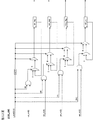
また、アクティブマトリクス方式の有機EL表示パネルは、画素16は発光素子であるEL素子15、第1のトランジスタ11a、第2のトランジスタ11bおよび蓄積容量19からなる。発光素子15は有機エレクトロルミネッセンス(EL)素子である。本発明では、EL素子15に電流を供給(制御)するトランジスタ11aを駆動用トランジスタ11と呼ぶ。
【0040】
有機EL素子15は多くの場合、整流性があるため、OLED(有機発光ダイオード)と呼ばれることがある。図1などでは発光素子15としてダイオードの記号を用いている。
【0041】
ただし、本発明における発光素子15はOLEDに限るものではなく、素子15に流れる電流量によって輝度が制御されるものであればよい。たとえば、無機EL素子が例示される。その他、半導体で構成される白色発光ダイオードが例示される。また、一般的な発光ダイオードが例示される。その他、発光トランジスタでもよい。また、発光素子15は必ずしも整流性が要求されるものではない。双方向性ダイオードであってもよい。本発明のEL素子15はこのいずれでもよい。
【0042】
近年、低消費電力でかつ高表示品質であり、更に薄型化が可能な表示パネルとして、有機エレクトロルミネッセンス(EL)素子の複数をマトリクス状に配列して構成される有機EL表示パネルが注目されている。
【0043】
有機EL表示パネルは、図10に示すように、画素電極としての透明電極105が形成されたガラス板71(アレイ基板)上に、電子輸送層、発光層、正孔輸送層などからなる少なくとも1層の有機機能層(EL層)15、及び金属電極(反射膜)(カソード)106が積層されたものである。
【0044】
透明電極(画素電極)105である陽極(アノード)にプラス、金属電極(反射電極)106の陰極(カソード)にマイナスの電圧を加え、すなわち、透明電極105及び金属電極106間に直流を印加することにより、有機機能層(EL層)15が発光する。良好な発光特性を期待することのできる有機化合物を有機機能層に使用することによって、EL表示パネルが実用に耐えうるものになっている。なお、本発明は有機EL表示パネルを例にして説明をするが、これに限定するものではない。無機ELを使用したディスプレイや、FED、もしくはSEDのような自発光素子を利用したディスプレイに適応することが可能である。また、構造、回路などはTN液晶表示パネル、STN液晶表示パネルなど、他の表示パネルにも適用できる事項がある。
【0045】
以下、本発明のEL表示パネルの製造方法および構造について詳しく説明をする。まず、アレイ基板71に画素を駆動するトランジスタ11を形成する。1つの画素は2個以上、好ましくは4個または5個のトランジスタで構成される。また、画素は電流プログラムされ、プログラムされた電流がEL素子15に供給される。通常、電流プログラムされた値は電圧値として蓄積容量19に保持される。このトランジスタ11の組み合わせなど画素構成については後に説明をする。次にトランジスタ11に正孔注入電極としての画素電極を形成する。画素電極105はフォトリソグラフィーによりパターン化する。なお、トランジスタ11の下層、あるいは上層にはトランジスタ11に光入射することにより発生するホトコンダクタ現象(以後、ホトコンと呼ぶ)による画質劣化を防止するために、遮光膜を形成または配置する。
【0046】
なお、電流プログラムとは、ソースドライバ回路14からプログラム電流を画素に印加し(もしくは画素からソースドライバ回路14に吸収し)、この電流に相当する信号値を画素に保持させるものである。この保持された信号値に対応する電流をEL素子15に流す(もしくは、EL素子15から流し込む)。つまり、電流でプログラムし、プログラムされた電流に相当(対応)する電流をEL素子15に流すようにするものである。
【0047】
一方、電圧プログラムとは、ソースドライバ回路14からプログラム電圧を画素に印加し、この電圧に相当する信号値を画素に保持させるものである。この保持された電圧に対応する電流をEL素子15に流す。つまり、電圧でプログラムし、画素内で電圧を電流値に変換し、プログラムされた電圧に相当(対応)する電流をEL素子15に流すようにするものである。
【0048】
まず、有機EL表示パネルに用いられるアクティブマトリックス方式は、1.特定の画素を選択し、必要な表示情報を与えられること。2、1フレーム期間を通じてEL素子に電流を流すことができることという2つの条件を満足させなければならない。
【0049】
この2つの条件を満足させるため、図76に図示する従来の有機ELの画素構成では、第1のトランジスタ11bは画素を選択するためのスイッチング用トランジスタ、第2のトランジスタ11aはEL素子(EL膜)15に電流を供給するための駆動用トランジスタとする。
【0050】
ここで液晶に用いられるアクティブマトリックス方式と比較すると、スイッチング用トランジスタ11bは液晶用にも必要であるが、駆動用トランジスタ11aはEL素子15を点灯させるために必要である。この理由は液晶の場合は、電圧を印加することでオン状態を保持することができるが、EL素子15の場合は、電流を流しつづけなければ画素16の点灯状態を維持できないからである。
【0051】
したがって、EL表示パネルでは電流を流し続けるためにトランジスタ11aをオンさせ続けなければならない。まず、走査線、データ線が両方ともオンになると、スイッチング用トランジスタ11bを通してキャパシタ19に電荷が蓄積される。このキャパシタ19が駆動用トランジスタ11aのゲートに電圧を加え続けるため、スイッチング用トランジスタ11bがオフになっても、電流供給線(Vdd)から電流が流れつづけ、1フレーム期間にわたり画素16をオンできる。
【0052】
この構成を用いて階調を表示させる場合、駆動用トランジスタ11aのゲート電圧として階調に応じた電圧を印加する必要がある。したがって、駆動用トランジスタ11aのオン電流のばらつきがそのまま表示に現れる。
【0053】
トランジスタのオン電流は単結晶で形成されたトランジスタであれば、きわめて均一であるが、安価なガラス基板に形成することのできる形成温度が450度以下の低温ポリシリ技術で形成した低温多結晶トタンジスタでは、そのしきい値のばらつきが±0.2V〜0.5Vの範囲でばらつきがある。そのため、駆動用トランジスタ11aを流れるオン電流がこれに対応してばらつき、表示にムラが発生する。これらのムラは、しきい値電圧のばらつきのみならず、トランジスタの移動度、ゲート絶縁膜の厚みなどでも発生する。また、トランジスタ11の劣化によっても特性は変化する。
【0054】
なお、低温ポリシリコン技術に限定されるものではなく、プロセス温度が450度(摂氏)以上の高温ポリシリコン技術を用いて構成してもよく、また、固相(CGS)成長させた半導体膜を用いてTFTなどを形成したものをもちいてもよい。その他、有機TFTを用いたものであっても良い。
【0055】
また、アモルファスシリコン技術で形成したTFTアレイを用いてパネルを構成する。なお、本明細書では低温ポリシリコン技術で形成したTFTを主として説明する。しかし、TFTのバラツキが発生するなどの課題は他の方式でも同一である。
【0056】
したがって、アナログ的に階調を表示させる方法では、均一な表示を得るために、デバイスの特性を厳密に制御する必要があり、現状の低温多結晶ポリシリコントランジスタではこのバラツキを所定範囲以内の抑えるというスペックを満足できない。この問題を解決するため、1画素内に4つ以上のトランジスタをもうけて、しきい値電圧のばらつきをコンデンサにより補償させて均一な電流を得る方法、定電流回路を1画素ごとに形成し電流の均一化を図る方法などが考えられる。
【0057】
しかしながら、これらの方法は、プログラムされる電流がEL素子15を通じてプログラムされるため電流経路が変化した場合に電源ラインに接続されるスイッチングトランジスタに対し駆動電流を制御するトランジスタがソースフォロワとなり駆動マージンが狭くなる。したがって、駆動電圧が高くなるという課題を有する。
【0058】
また、電源に接続するスイッチングトランジスタをインピーダンスの低い領域で使用する必要があり、この動作範囲がEL素子15の特性変動により影響を受けるという課題もある。その上、飽和領域における電圧電流特性に、キンク電流が発生する場合、トランジスタのしきい値電圧の変動が発生した場合、記憶された電流値が変動するとう課題もある。
【0059】
本発明のEL素子構造は、上記課題に対して、EL素子15に流れる電流を制御するトランジスタ11が、ソースフォロワ構成とならず、かつそのトランジスタにキンク電流があっても、キンク電流の影響を最小に抑えることが出来て記憶される電流値の変動を小さくすることが出来る構成である。
【0060】
本発明のEL表示装置の画素構造は、具体的には図1に示すように単位画素が最低4つからなる複数のトランジスタ11ならびにEL素子により形成される。なお、画素電極はソース信号線と重なるように構成する。つまり、ソース信号線18上に絶縁膜あるいはアクリル材料からなる平坦化膜を形成して絶縁し、この絶縁膜上に画素電極105を形成する。このようにソース信号線18上に画素電極を重ねる構成をハイアパーチャ(HA)構造と呼ぶ。
【0061】
ゲート信号線(第1の走査線)17aをアクティブ(ON電圧を印加)とすることによりEL素子15駆動用のトランジスタ(トランジスタあるいはスイッチング素子)11aおよびトランジスタ(トランジスタあるいはスイッチング素子)11cを通して、前記EL素子15に流すべき電流値をソースドライバ回路14から流す。また、トランジスタ11aのゲートとドレイン間を短絡するようにトランジスタ11bがゲート信号線17aアクティブ(ON電圧を印加)となることにより開くと共に、トランジスタ11aのゲートとソース間に接続されたコンデンサ(キャパシタ、蓄積容量、付加容量)19に、前記電流値を流すようにトランジスタ11aのゲート電圧(あるいはドレイン電圧)を記憶する(図3(a)を参照のこと)。
【0062】
なお、トランジスタ11aのソース(S)−ゲート(G)間容量(コンデンサ)19は0.2pF以上の容量とすることが好ましい。他の構成として、別途、コンデンサ19を形成する構成も例示される。つまり、コンデンサ電極レイヤーとゲート絶縁膜およびゲートメタルから蓄積容量を形成する構成である。トランジスタ11cのリークによる輝度低下を防止する観点、表示動作を安定化させるための観点からはこのように別途コンデンサを構成するほうが好ましい。なお、コンデンサ(蓄積容量)19の大きさは、0.2pF以上2pF以下とすることがよく、中でもコンデンサ(蓄積容量)19の大きさは、0.4pF以上1.2pF以下とすることがよい。
【0063】
なお、コンデンサ19は隣接する画素間の非表示領域におおむね形成することがこのましい。一般的に、フルカラー有機EL15を作成する場合、有機EL層15をメタルマスクによるマスク蒸着で形成するためマスク位置ずれによるEL層の形成位置が発生する。位置ずれが発生すると各色の有機EL層15(15R、15G、15B)が重なる危険性がある。そのため、各色の隣接する画素間の非表示領域は10μ以上離れなければならない。この部分は発光に寄与しない部分となる。
したがって、蓄積容量19をこの領域に形成することは開口率向上のために有効な手段となる。
【0064】
なお、メタルマスクは磁性体で作製し、基板71の裏面から磁石でメタルマスクを磁力で吸着する。磁力により、メタルマスクは基板と隙間なく密着する。以上の製造方法に関する事項は、本発明の他の製造方法にも適用される。
【0065】
次に、ゲート信号線17aを非アクティブ(OFF電圧を印加)、ゲート信号線17bをアクティブとして、電流の流れる経路を前記第1のトランジスタ11a並びにEL素子15に接続されたトランジスタ11dならびに前記EL素子15を含む経路に切り替えて、記憶した電流を前記EL素子15に流すように動作する(図3(b)を参照のこと)。
【0066】
この回路は1画素内に4つのトランジスタ11を有しており、トランジスタ11a のゲートはトランジスタ11bのソースに接続されている。また、トランジスタ11bおよびトランジスタ11cのゲートはゲート信号線17aに接続されている。トランジスタ11bのドレインはトランジスタ11cのソースならびにトランジスタ11dのソースに接続され、トランジスタ11cのドレインはソース信号線18に接続されている。トランジスタ11dのゲートはゲート信号線17bに接続され、トランジスタ11dのドレインはEL素子15のアノード電極に接続されている。
【0067】
なお、図1ではすべてのトランジスタはPチャンネルで構成している。Pチャンネルは多少Nチャンネルのトランジスタに比較してモビリティが低いが、耐圧が大きくまた劣化も発生しにくいので好ましい。しかし、本発明はEL素子構成をPチャンネルで構成することのみに限定するものではない。Nチャンネルのみで構成してもよい。また、NチャンネルとPチャンネルの両方を用いて構成してもよい。
【0068】
なお、図1においてトランジスタ11c、11bは同一の極性で構成し、かつNチャンネルで構成し、トランジスタ11a、11dはPチャンネルで構成することが好ましい。一般的にPチャンネルトランジスタはNチャンネルトランジスタに比較して、信頼性が高い、キンク電流が少ないなどの特長があり、電流を制御することによって目的とする発光強度を得るEL素子15に対しては、トランジスタ11aをPチャンネルにする効果が大きい。最適には画素を構成するTFT11をすべてPチャンネルで形成し、内蔵ゲートドライバ12もPチャンネルで形成することが好ましい。このようにアレイをPチャンネルのみのTFTで形成することにより、マスク枚数が5枚となり、低コスト化、高歩留まり化を実現できる。
【0069】
以下、さらに本発明の理解を容易にするために、本発明のEL素子構成について図3を用いて説明する。本発明のEL素子構成は2つのタイミングにより制御される。第1のタイミングは必要な電流値を記憶させるタイミングである。このタイミングでトランジスタ11bならびにトランジスタ11cがONすることにより、等価回路として図3(a)となる。ここで、信号線より所定の電流Iwが書き込まれる。これによりトランジスタ11aはゲートとドレインが接続された状態となり、このトランジスタ11aとトランジスタ11cを通じて電流Iwが流れる。従って、トランジスタ11aのゲートーソースの電圧はI1が流れるような電圧V1となる。
【0070】
第2のタイミングはトランジスタ11aとトランジスタ11cが閉じ、トランジスタ11dが開くタイミングであり、そのときの等価回路は図3(b)となる。トランジスタ11aのソース−ゲート間の電圧は保持されたままとなる。この場合、トランジスタ11aは常に飽和領域で動作するため、Iwの電流は一定となる。
【0071】
このように動作させると、図5に図示するようになる。つまり、図5(a)の51aは表示画面50における、ある時刻での電流プログラムされている画素(行)(書き込み画素行)を示している。この画素(行)51aは、図5(b)に図示するように非点灯(非表示画素(行))とする。他の、画素(行)は表示画素(行)53とする(非画素53のEL素子15には電流が流れ、EL素子15が発光している)。
【0072】
図1の画素構成の場合、図3(a)に示すように、電流プログラム時は、プログラム電流Iwがソース信号線18に流れる。この電流Iwがトランジスタ11aを流れ、Iwを流す電流が保持されるように、コンデンサ19に電圧設定(プログラム)される。このとき、トランジスタ11dはオープン状態(オフ状態)である。
【0073】
次に、EL素子15に電流を流す期間は図3(b)のように、トランジスタ11c、11bがオフし、トランジスタ11dが動作する。つまり、ゲート信号線17aにオフ電圧(Vgh)が印加され、トランジスタ11b、11cがオフする。一方、ゲート信号線17bにオン電圧(Vgl)が印加され、トランジスタ11dがオンする。
【0074】
このタイミングチャートを図4に図示する。なお、図4などにおいて、括弧内の添え字(たとえば、(1)など)は画素行の番号を示している。つまり、ゲート信号線17a(1)とは、画素行(1)のゲート信号線17aを示している。また、図4の上段の*Hとは、水平走査期間を示している。つまり、1Hとは第1番目の水平走査期間である。なお、以上の事項は、説明を容易にするためであって、限定(1Hの番号、1H周期、画素行番号の順番など)するものではない。
【0075】
図4でわかるように、各選択された画素行(選択期間は、1Hとしている)において、ゲート信号線17aにオン電圧が印加されている時には、ゲート信号線17bにはオフ電圧が印加されている。また、この期間は、EL素子15には電流が流れていない(非点灯状態)。選択されていない画素行において、ゲート信号線17aにオフ電圧が印加され、ゲート信号線17bにはオン電圧が印加されている。また、この期間は、EL素子15に電流が流れている(点灯状態)。
【0076】
なお、トランジスタ11bのゲートとトランジスタ11cのゲートは同一のゲート信号線17aに接続している。しかし、トランジスタ11bのゲートとトランジスタ11cのゲートとを異なるゲート信号線17に接続してもよい。1画素のゲート信号線は3本となる(図1の構成は2本である)。トランジスタ11bのゲートのON/OFFタイミングとトランジスタ11cのゲートのON/OFFタイミングを個別に制御することにより、トランジスタ11aのばらつきによるEL素子15の電流値バラツキをさらに低減することができる。
【0077】
ゲート信号線17aとゲート信号線17bとを共通にし、トランジスタ11cと11dが異なった導電型(NチャンネルとPチャンネル)とすると、駆動回路の簡略化、ならびに画素の開口率を向上させることが出来る。
【0078】
このように構成すれば本発明の動作タイミングとしては信号線からの書きこみ経路がオフになる。すなわち所定の電流が記憶される際に、電流の流れる経路に分岐があると正確な電流値がトランジスタ11aのソース(S)−ゲート(G)間容量(コンデンサ)に記憶されない。トランジスタ11cとトランジスタ11dを異なった導電形にすることにより、お互いの閾値を制御することによって走査線の切り替わりのタイミングで必ずトランジスタ11cがオフしたのちに、トランジスタ11dがオンすることが可能になる。
【0079】
本特許の発明の目的は、トランジスタ特性のばらつきが表示に影響を与えない回路構成を提案するものであり、そのために4トランジスタ以上が必要である。これらのトランジスタ特性により、回路定数を決定する場合、4つのトランジスタの特性がそろわなければ、適切な回路定数を求めることが困難である。レーザー照射の長軸方向に対して、チャンネル方向が水平の場合と垂直の場合では、トランジスタ特性の閾値と移動度が異なって形成される。なお、どちらの場合もばらつきの程度は同じである。水平方向と、垂直方向では移動度、閾値のあたいの平均値が異なる。したがって、画素を構成するすべてのトランジスタのチャンネル方向は同一であるほうが望ましい。
【0080】
図27においてEL素子15に流す電流を設定する時、トランジスタ271aに流す信号電流をIw、その結果トランジスタ271aに生ずるゲートーソース間電圧をVgsとする。書き込み時はトランジスタ11cによってトランジスタ271aのゲート・ドレイン間が短絡されているので、トランジスタ271aは飽和領域で動作する。よって、Iwは、以下の式で与えられる。
(数1)
Iw
=μ1・Cox1・{W1/(2・L1)}・(Vgs−Vth1)2
ここで、Coxは単位面積当たりのゲート容量であり、Cox=ε0・εr/dで与えられる。Vthはトランジスタの閾値、μはキャリアの移動度、Wはチャンネル幅、Lはチャンネル長、ε0は真空の移動度、εrはゲート絶縁膜の比誘電率を示し、dはゲート絶縁膜の厚みである。
EL素子15に流れる電流をIddとすると、Iddは、EL素子15と直列に接続されるトランジスタ271bによって電流レベルが制御される。本発明では、そのゲートーソース間電圧が(数1)のVgsに一致するので、トランジスタ1bが飽和領域で動作すると仮定すれば、以下の式が成り立つ。
(数2)
Idrv
=μ2・Cox2・{W2/(2・L2)}・(Vgs−Vth2)2
絶縁ゲート電界効果型の薄膜トランジスタ(トランジスタ)が飽和領域で動作するための条件は、Vdsをドレイン・ソース間電圧として、一般に以下の式で与えられる。
(数3)
|Vds|>|Vgs−Vth|
ここで、トランジスタ271aとトランジスタ271bは、小さな画素内部に近接して形成されるため、大略μ1=μ2及びCox1=Cox2であり、特に工夫を凝らさない限り、Vth1=Vth2と考えられる。すると、このとき(数1)及び(数2)から容易に以下の式が導かれる。
【0081】
(数4)
Idrv/Iw=(W2/L2)/(W1/L1)
ここで注意すべき点は、(数1)及び(数2)において、μ、Cox、Vthの値自体は、画素毎、製品毎、あるいは製造ロット毎にばらつくのが普通であるが、(数4)はこれらのパラメータを含まないので、Idrv/Iwの値はこれらのばらつきに依存しないということである。
【0082】
仮にW1=W2、L1=L2と設計すれば、Idrv/Iw=1、すなわちIwとIdrvが同一の値となる。すなわちトランジスタの特性ばらつきによらず、EL素子15に流れる駆動電流Iddは、正確に信号電流Iwと同一になるので、結果としてEL素子15の発光輝度を正確に制御できる。
【0083】
以上の様に、駆動用トランジスタ271aのVth1と駆動用トランジスタ271bのVth2は基本的に同一である為、両トランジスタお互いにの共通電位にあるゲートに対してカットオフレベルの信号電圧が印加されると、トランジスタ271a及びトランジスタ271b共に非導通状態になるはずである。ところが、実際には画素内でもパラメータのばらつきなどの要因により、Vth1よりもVth2が低くなってしまうことがある。この時には、駆動用トランジスタ271bにサブスレッショルドレベルのリーク電流が流れる為、EL素子15は微発光を呈する。この微発光により画面のコントラストが低下し表示特性が損なわれる。
【0084】
本発明では特に、駆動用トランジスタ271bの閾電圧Vth2が画素内で対応する駆動用トランジスタ271aの閾電圧Vth1より低くならない様に設定している。例えば、トランジスタ271bのゲート長L2をトランジスタ271aのゲート長L1よりも長くして、これらの薄膜トランジスタのプロセスパラメータが変動しても、Vth2がVth1よりも低くならない様にする。これにより、微少な電流リークを抑制することが可能である。以上の事項は図1のトランジスタ271aとトランジスタ11cの関係にも適用される。
【0085】
図27に示すように、信号電流が流れる駆動用トランジスタ271a、EL素子15等からなる発光素子に流れる駆動電流を制御する駆動用トランジスタ271bの他、ゲート信号線17a1の制御によって画素回路とデータ線dataとを接続もしくは遮断する取込用トランジスタ11b、ゲート信号線17a2の制御によって書き込み期間中にトランジスタ271aのゲート・ドレインを短絡するスイッチ用トランジスタ11c、トランジスタ271aのゲート−ソース間電圧を書き込み終了後も保持するための容量C19および発光素子としてのEL素子15などから構成される。
【0086】
図27でトランジスタ11b、11cはNチャンネルMOS(NMOS)、その他のトランジスタはPチャンネルMOS(PMOS)で構成しているが、これは一例であって、必ずしもこの通りである必要はない。容量Cは、その一方の端子をトランジスタ271aのゲートに接続され、他方の端子はVdd(電源電位)に接続されているが、Vddに限らず任意の一定電位でも良い。EL素子15のカソード(陰極)は接地電位に接続されている。したがって、以上の事項は図1などにも適用されることは言うまでもない。
【0087】
なお、図1などのVdd電圧はトランジスタ271bのオフ電圧(トランジスタがPチャンネル時)よりも低くすることが好ましい。具体的には、Vgh(ゲートのオフ電圧)は少なくともVdd−0.5(V)よりの高くするべきである。これよりも低いとトランジスタのオフリークが発生し、レーザーアニ−ルのショットムラが目立つようになる。また、Vdd+4(V)よりも低くすべきである。あまりにも高いと逆にオフリーク量が増加する。
【0088】
したがって、ゲートのオフ電圧(図1ではVgh、つまり、電源電圧に近い電圧側)は、電源電圧(図1ではVdd)は、−0.5(V)以上+4(V)以下とすべきである。さらに好ましくは、電源電圧(図1ではVdd)は、0(V)以上+2(V)以下とすべきである。つまり、ゲート信号線に印加するトランジスタのオフ電圧は、十分オフになるようにする。トランジスタがNチャンネルの場合は、Vglがオフ電圧となる。したがって、VglはGND電圧に対して−4(V)以上0.5(V)以下の範囲となるようにする。さらに好ましくは−2(V)以上0(V)以下の範囲することが好ましい。
【0089】
以上の事項は、図1の電流プログラムの画素構成について述べたが、これに限定するものではなく、電圧プログラムの画素構成にも適用できることは言うまでもない。なお、電圧プログラムのVtオフセットキャンセルは、R、G、Bごとに個別に補償することが好ましい。
【0090】
駆動用トランジスタ271bは、コンデンサ19に保持された電圧レベルをゲートに受け入れそれに応じた電流レベルを有する駆動電流はチャネルを介してEL素子15に流す。トランジスタトランジスタ271aのゲートとトランジスタトランジスタ271bのゲートとが直接に接続されてカレントミラー回路を構成し、信号電流Iwの電流レベルと駆動電流の電流レベルとが比例関係となる様にしている。
【0091】
トランジスタ271bは飽和領域で動作し、そのゲートに印加された電圧レベルと閾電圧との差に応じた駆動電流をEL素子15に流す。
【0092】
トランジスタ271bは、その閾電圧が画素内で対応するランジスタ271aの閾電圧より低くならない様に設定されている。具体的には、トランジスタ271bは、そのゲート長がトランジスタ271aのゲート長より短くならない様に設定されている。あるいは、トランジスタ271bは、そのゲート絶縁膜が画素内で対応するトランジスタ271aのゲート絶縁膜より薄くならないように設定しても良い。
【0093】
あるいは、トランジスタ271bは、そのチャネルに注入される不純物濃度を調整して、閾電圧が画素内で対応するトランジスタ271aの閾電圧より低くならない様に設定してもよい。仮に、トランジスタ271aとトランジスタ271bの閾電圧が同一となる様に設定した場合、共通接続されたトランジスタのゲートにカットオフレベルの信号電圧が印加されると、トランジスタ271a及びトランジスタ271bは両方共オフ状態になるはずである。ところが、実際には画素内にも僅かながらプロセスパラメータのばらつきがあり、トランジスタ271aの閾電圧よりトランジスタ271bの閾電圧が低くなる場合がある。
【0094】
この時には、カットオフレベル以下の信号電圧でもサブスレッショルドレベルの微弱電流が駆動用トランジスタ271bに流れる為、EL素子15は微発光し画面のコントラスト低下が現れる。そこで、トランジスタ271bのゲート長をトランジスタ271aのゲート長よりも長くしている。これにより、トランジスタ11のプロセスパラメータが画素内で変動しても、トランジスタ271bの閾電圧がトランジスタ271aの閾電圧よりも低くならない様にする。
【0095】
ゲート長Lが比較的短い短チャネル効果領域Aでは、ゲート長Lの増加に伴いVthが上昇する。一方、ゲート長Lが比較的大きな抑制領域Bではゲート長Lに関わらずVthはほぼ一定である。この特性を利用して、トランジスタ271bのゲート長をトランジスタ271aのゲート長よりも長くしている。例えば、トランジスタ271aのゲート長が7μmの場合、トランジスタ271bのゲート長を10μm程度にする。
【0096】
トランジスタ271aのゲート長が短チャネル効果領域Aに属する一方、トランジスタ271bのゲート長が抑制領域Bに属する様にしても良い。これにより、トランジスタ271bにおける短チャネル効果を抑制することができるとともに、プロセスパラメータの変動による閾電圧低減を抑制可能である。以上により、トランジスタ271bに流れるサブスレッショルドレベルのリーク電流を抑制してEL素子15の微発光を抑え、コントラスト改善に寄与可能である。
【0097】
このようにして作製した図1、図2、図27などで説明したEL表示素子15に直流電圧を印加し、10mA/cm2の一定電流密度で連続駆動させた。EL構造体は、7.0V 、200cd/cm2の緑色(発光極大波長λmax =460nm)の発光が確認できた。青色発光部は、輝度100cd/cm2で、色座標がx=0.129、y=0.105、緑色発光部は、輝度200cd/cm2で、色座標がx=0.340、y=0.625、赤色発光部は、輝度100cd/cm2で、色座標がx=0.649、y=0.338の発光色が得られた。
【0098】
フルカラー有機EL表示パネルでは、開口率の向上が重要な開発課題になる。開口率を高めると光の利用効率が上がり、高輝度化や長寿命化につながるためである。開口率を高めるためには、有機EL層からの光を遮るトランジスタの面積を小さくすればよい。低温多結晶Si−トランジスタはアモルファスシリコンに比較して10−100倍の性能を持ち、電流の供給能力が高いため、トランジスタの大きさを非常に小さくできる。したがって、有機EL表示パネルでは、画素トランジスタ、周辺駆動回路を低温ポリシリコン技術、高温ポリシリコン技術で作製することが好ましい。もちろん、アモルファスシリコン技術で形成してもよいが画素開口率はかなり小さくなってしまう。
【0099】
ゲートドライバ回路12あるいはソースドライバ回路14などの駆動回路をガラス基板71上に形成することにより、電流駆動の有機EL表示パネルで特に問題になる抵抗を下げることができる。TCPの接続抵抗がなくなるうえに、TCP接続の場合に比べて電極からの引き出し線が2〜3mm短くなり配線抵抗が小さくなる。さらに、TCP接続のための工程がなくなる、材料コストが下がるという利点があるとする。
【0100】
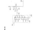
次に、本発明のEL表示パネルあるいはEL表示装置について説明をする。図6はEL表示装置の回路を中心とした説明図である。画素16がマトリックス状に配置または形成されている。各画素16には各画素の電流プログラムを行う電流を出力するソースドライバ回路14が接続されている。ソースドライバ回路14の出力段は映像信号のビット数に対応したカレントミラー回路が形成されている(後に説明する)。たとえば、64階調であれば、63個のカレントミラー回路が各ソース信号線に形成され、これらのカレントミラー回路の個数を選択することにより所望の電流をソース信号線18に印加できるように構成されている。
【0101】
なお、1つのカレントミラー回路の1つの単位トランジスタの最小出力電流は10nA以上50nA以下にしている。特にカレントミラー回路の最小出力電流は15nA以上35nA以下にすることがよい。ソースドライバIC14内のカレントミラー回路を構成するトランジスタの精度を確保するためである。
【0102】
また、ソース信号線18の電荷を強制的に放出または充電するプリチャージあるいはディスチャージ回路を内蔵する。ソース信号線18の電荷を強制的に放出または充電するプリチャージあるいはディスチャージ回路の電圧(電流)出力値は、R、G、Bで独立に設定できるように構成することが好ましい。EL素子15の閾値がRGBでことなるからである。
【0103】
以上に説明した画素構成、アレイ構成、パネル構成などは、以下に説明する構成、方法、装置に適用されることは言うまでもない。また、以下に説明する構成、方法、装置は、すでに説明した画素構成、アレイ構成、パネル構成などが適用されることは言うまでもない。
【0104】
ゲートドライバ12はゲート信号線17a用のシフトレジスタ回路61aと、ゲート信号線17b用のシフトレジスタ回路61bとを内蔵する。各シフトレジスタ回路61は正相と負相のクロック信号(CLKxP、CLKxN)、スタートパルス(STx)で制御される。その他、ゲート信号線の出力、非出力を制御するイネーブル(ENABL)信号、シフト方向を上下逆転するアップダウン(UPDWM)信号を付加することが好ましい。他に、スタートパルスがシフトレジスタにシフトされ、そして出力されていることを確認する出力端子などを設けることが好ましい。
【0105】
なお、シフトレジスタのシフトタイミングはコントロールIC81からの制御信号で制御される。 また、外部データのレベルシフトを行うレベルシフト回路を内蔵する。また、検査回路を内蔵する。
【0106】
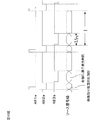
図8は本発明の表示装置の信号、電圧の供給の構成図あるいは表示装置の構成図である。コントロールIC81からソースドライバ回路14aに供給する信号(電源配線、データ配線など)はフレキシブル基板84を介して供給する。
【0107】
図8ではゲートドライバ12の制御信号はコントロールICで発生させ、ソースドライバ14でいったん、レベルシフトを行った後、ゲートドライバ12に印加している。ソースドライバ14の駆動電圧は4〜8(V)であるから、コントロールIC81から出力された3.3(V)振幅の制御信号を、ゲートドライバ12が受け取れる5(V)振幅に変換することができる。
【0108】
以下、本発明の駆動方法について説明する。本発明は有機ELパネルの駆動に特化した輝度調整駆動である。有機EL素子は蓄積容量19に蓄積された電荷とVddに応じて駆動トランジスタ11aが流す電流量に比例して発光する。そのため、図12に示すようにパネルに流れる総電流とパネルの明るさの関係はリニアになる。有機EL素子に電流を流すための電圧Vddは図24に示すようにバッテリー241によって供給される。
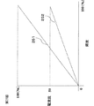
【0109】
このバッテリー241には容量の制限があり、特に小型モジュールに使用する場合流すことの出来る電流量は少なくなる。仮に、図25に示すようにバッテリー241が有機ELパネルの消費する電力の50%までしか流すことができないとする。ここで251に示すような直線で有機ELが発する明るさ(全面白表示を100%とする)と電力の関係を決めると明るさの高い領域ではバッテリーの流せる最大の電流量を超えてしまうため、バッテリーを破壊してしまう恐れがある。
【0110】
反対に252に示すように有機ELパネルの最大発光時に流れる電流量と、バッテリー241が流すことが出来る最大電流量を同じ値にして明るさと電力の関係を決めると低輝度部において電流を流すことが出来なくなる。一般に映像データは全面白表示状態を100%とすると、30%辺りが多いと言われている。252に示すような明るさと電流量の関係にすると、映像データの多い領域で電流を流すことが出来なくなり、見栄えのしない画像になってしまう。
【0111】
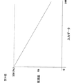
そこで本発明では図26に示すように特定の入力データを設定し、そのデータに応じて、有機ELパネルに流れる電流量を調整する駆動を提案する。バッテリーの限界値を超える可能性がある領域では電流値を抑制し、電流があまり流れない領域では電流量を増やす駆動方法である。この駆動方法を実現すると有機ELパネルの明るさと電流量の関係は282のようになり、バッテリーの容量制限があっても映像データの多い領域で電流を流すことが可能となり、見栄えの良い画像を作ることができる。本発明の内容は2種類の駆動方法を組み合わせたもので、以下その駆動方法と適用される回路構成を説明する。第1の駆動方法は、従来の一般的な駆動方法と同様に外部からの入力映像データと自己発光素子を用いた表示装置の画面の輝度、もしくは自己発光素子のアノード電極とカソード電極の間に流れる電流量の関係が1:1に対応、すなわち1つの入力映像データに対して取り得る電流量の値は1つであり予め定められた値であり、外部からの入力映像信号に応じた第1の輝度で各表示画素を発光させる。またそれらは比例の関係にあり、理想的には線形的に比例する。本発明では特に低階調側(黒表示側)の駆動に適用した場合を説明する。
一方第2の駆動方法は、外部からの入力映像データと自己発光素子を用いた表示装置の画面の輝度、もしくは自己発光素子のアノード電極とカソード電極の間に流れる電流量の関係を1対1に対応させるのではなく、周辺の入力映像データの分布状況を考慮した電流量を決定、すなわち可変値の中から定められたある値に決定される。従って先程の第1の駆動と異なり、線形的な比例関係になるとは限らず、非線形な関係になることが多い。このとき外部からの入力映像信号に応じた第1の輝度を所定の割合で抑制した第2の輝度で各表示画素を発光させる。従って先程の第1の駆動と異なり、線形的な比例関係になるとは限らず、非線形な関係になることが多い。
【0112】
第2の駆動方法では電流量の値は、まず外部から入力される映像データに対して第1の駆動方法を施したと仮定したときの電流量を1としたときに、ある所定の定数(1以下の数)を乗して抑制された電流量として得ることができる。定数の値については周辺の入力映像データの分布状況により都度決定される。また、前に述べたように映像データが多い領域では電流を多く流したいため、抑制処理を行わない場合の最大入力データに対する電力、もしくは電流量を1とすると、第2の駆動を適用する領域において、電力値xが0.2≦x≦0.6になるように電力、もしくは電流量を調整することを特徴とする駆動方法である。
【0113】
尚、第2の駆動を行う回路にスイッチング手段を設け、第2の駆動手段の入切を制御することで、第2の駆動手段を入れた場合は本発明の駆動方法を行い、また第2の駆動手段を切った場合には従来の駆動方法と互換性を持たせることができる。
【0114】
電流値を調整する方法として二つの方法を提案する。一つはソース信号線18に流す電流量を減らし、有機EL素子に流れる電流量自体を調整する方法である。しかし、この方法は電流量を抑制する際にはソース信号線18に流れる電流量を少なくしなくてはならない。前に示したように有機EL素子は蓄積容量19に蓄積された電荷に応じて発光する。入力されたデータを正しく発光させるためには蓄積容量19に正しい電流値を流せるような電荷を蓄積する必要がある。
【0115】
しかし、実際ソース信号線18には浮遊容量451が存在する。V2からV1までソース信号線電圧を変化させるにはこの浮遊容量の電荷を引き抜く必要がある。この引き抜きにかかる時間ΔTは、ΔQ(浮遊容量の電荷)=I(ソース信号線に流れる電流)×ΔT=C(浮遊容量値)×ΔVとなる。このため、電流値Iを減少させると蓄積容量19に正しい電荷を蓄積させることが出来なくなる。また、電流値を減少させると、階調表現が困難になる。階調を1024階調で表現させようと考えると黒を表示させるための電流値と白を表現させる電流値の差を1024等分する必要がある。そのため、白を表現させる電流値をへらすと1階調あたりの電流変化量が小さくなり、階調表現をするための精度が高くなり、実現が難しくなる。
【0116】
まず、映像を判断するための表示データについて説明をする。表示データは、画像データあるいはパネルの消費電流(アノード電極とカソード電極の間に流れる電流)から導出する。本発明中では表示データを%で示している。100%は表示データの最大値、つまり全ての画素が最高階調で発光する状態であり、0%は全ての画素が最低階調で発光する状態である。
【0117】
1画面の画像データが全体的に大きいときは画像データの総和は大きくなる。たとえば、白ラスターは64階調表示の場合は画像データとしては63であるから、画面50の画素数×63が画像データの総和である。1/100の白ウインドウ表示で、白表示部が最大輝度の白表示では、画面50の画素数×(1/100)×63が画像データの総和である(データ和の最大値である)。
【0118】
本発明では画像データの総和あるいは画面の消費電流量を予測できる値を求め、この総和あるいは値により、自己発光素子のアノード電極とカソード電極の間に流れる電流量を抑制する駆動を行う。
【0119】
なお、画像データの総和を求めるとしたが、これに限定するものではない。たとえば、画像データの1フレームの平均レベルを求めてこれを用いてもよい。アナログ信号であれば、アナログ画像信号をコンデンサによりフィルタリングすることにより平均レベルを得ることができる。アナログの映像信号に対しフィルタを介して直流レベルを抽出し、この直流レベルをAD変換して画像データの総和としてもよい。この場合は、画像データはAPLレベルとも言うことができる。
【0120】
本発明中には表示データを入力データと書いている場合があるが、これは同義語である。
【0121】
また、画面を構成する画像のすべてのデータを加算する必要はなく、画面の1/W(Wは1より大きい値)をピックアップして抽出し、ピックアップしたデータの総和を求めてもよい。
【0122】
データ和/最大値は表示データ(入力データ)の比率と同義である。データ和/最大値が1であれば、入力データが100%である(基本的に最大の白ラスター表示)。データ和/最大値が0であれば、入力データが0%である(基本的に完全黒ラスター表示である)。
【0123】
データ和/最大値は、映像データの和から求める。入力映像信号がY、U、Vの場合は、Y(輝度)信号から求めても良い。しかし、ELパネルの場合は、R、G、Bで発光効率が異なるため、Y信号から求めた値が消費電力にならない。したがって、Y、U、V信号の場合も、一度R、G、B信号に変換し、R、G、Bに応じて電流に換算する係数をかけて、消費電流(消費電力)を求めることが好ましい。しかし、簡易的にY信号から消費電流を求めることは回路処理が容易になることも考慮してもよい。
【0124】
表示データの比率を精度良く求めるためには演算を行うと良い。演算とは加算、減算、乗算、除算をふくむものである。
【0125】
また、有機ELパネルに流れる電流値を外部回路により測定し、フィードバックすることにより判断する方法も可能である。同様に有機ELパネル内にサーミスタもしくは熱電対などの温度センサーやフォトセンサーを内蔵することにより得られるデータを利用することも可能である。
【0126】
表示データは、パネルに流れる電流、つまり自己発光素子のアノード電極とカソード電極の間に流れる電流量で換算されているものであるとする。なぜなら、EL表示パネルではBの発光効率が悪いため、海の表示などが表示されると、消費電力が一気に増加するからである。したがって、最大値は、電源容量の最大値である。また、データ和とは単純な映像データの加算値ではなく、映像データを消費電流に換算したものとしている。したがって、点灯率も最大電流に対する各画像の使用電流から求められたものである。
【0127】
二つ目はソース信号線に流す電流値Iはそのままに1画面に点灯している水平走査線数(点灯率)を変えることで明るさを制御する。有機ELパネルはトランジスタ11dのON時間を制御することで水平走査線の1フレーム内の点灯時間を制御することができる。図14に示すようにゲートドライバー12を制御して1フレーム内の1/N期間しか点灯させないような駆動をすると、明るさは全ての水平走査線が常に点灯している場合の明るさに対して1/Nになる。この方法により明るさを調整することが可能である。この方法では発光している期間で明るさを制御するため、発光量を制御しても階調表現を実現するためのソース信号線に流れる電流値に求められる精度は変わらないので階調表現を容易に実現できる。そのため、本発明では点灯率を制御することにより有機ELパネルに流れる電流量を抑制する駆動方法を提案する。
【0128】
点灯率と入力データの関係は比例関係だけとは限らない。図29に示すように曲線や、折れ線にすることも可能である。291のように一定期間点灯率の高い状況を持続し、その後データに応じて点灯率を低くして行く形は一般的に映像データの明るさが30%(全面白表示が100%)のあたりが多い点を考えると有効であると言える。仮にバッテリー241の容量が有機ELパネルに流すことが出来る最大電流量の50%まで流すことが可能だとすると、入力データが最大の50%の領域まで点灯率を最大にしておいてもバッテリーを破壊することはない。
【0129】
また、明るさを制御するのに必ずしもトランジスタ11dを完全にOFFする必要はない。トランジスタ11dに少量の電流が流れ、有機EL素子15が微発光している状態でも明るさを抑制することは可能である。
【0130】
また、非発光、もしくは微発光期間は有機EL素子15を非発光、または微発光にするものであってトランジスタ11dのONとOFFで生成するのにかぎるものではない。例えば、図132、もしくは図133に示すようにトランジスタ11dが無い構成でもアノード電圧、もしくはカソード電圧を上下させることにより非発光、もしくは微発光期間を生成することが可能である。
【0131】
また、有機EL素子15に印加される電流を制御することが本発明であるので、図76に示すような回路構成でも761gを制御するのと同じことである。
【0132】
また、明るさを制御するための非発光部は水平走査線、つまり画素行方向に限るものではない。ソースドライバー14を制御して、画素列方向に非発光、もしくは微発光の期間を作り出すことで明るさの制御を行うことが可能である。
【0133】
微発光、もしくは非発光の期間をつくることにより、表示映像の中に画素列方向、もしくは画素行方向に微発光、もしくは非発光の表示ができる。この微発光、もしくは非発光の表示を表示映像の中に入れることを黒挿入と呼ぶ。
【0134】
また、入力データは最小と最大の間を2のn乗で刻むことが望ましい。例えば、全面黒点灯を0とすると、全面白点灯は256(2の8乗)とすると言ったやり方である。点灯率の変化を演算する際に変化量を求めるには最大点灯率と最小点灯率を入力データで割る必要がある。半導体設計において除算回路を組み込むことは回路構成において非常に大きい負荷である。その際に全面白表示時を2のn乗としておくと傾きは最大点灯率と最小点灯率の差を2進数にして8ビット分シフトするだけで求められるので半導体設計の観点から考えると除算回路を組み込む必要が無くなり、回路設計が非常に容易になる。291のような、一定期間最大点灯率を保った後、点灯率を徐々に下げて行くような波形を実現する際も、図30に示すように入力データの最小から2のn´乗までの間点灯率が最大になるような波形では、()のような直線型のグラフにおいて傾きをxとすると2のn´乗から2の(n´+1)乗までの期間だけ傾きを2xとすることで直線型のグラフと交わる。この構造を用いることにより、直線型の傾きを求めるだけで、折れ線型のグラフにした際も傾きを求めなおす必要が無くなり、回路規模を大きくせずに様々な折れ線型のグラフを作成することが可能になる。これは回路設計において回路規模を小さく構成するというメリットがある。
【0135】
続いて図55にて本駆動を実現するための回路構成について説明する。まず最初に映像ソースより、RGBの色データが551に入力される。同じデータはγ処理などの画像処理を経てソースドライバー14に入力される。図ではRGBの色データを書いているが、RGBに限るものではない。YUVの信号であることも考えられるし、前述のサーミスタやフォトセンサーから得られる温度データや輝度データでも良い。551でデータを拡張した後、データを収集するモジュール552にデータを入力する。551のデータの拡張に関しては後述で説明する。552でははじめにデータが加算器552aに入力される。ただし、常にデータが来ているわけではなく場合によっては画像データ以外の不定なデータが来ている可能性もある。そのため、加算器552aはデータが来ているかどうかのイネーブル信号(DE)と、クロック(CLK)により加算するかどうかを決定する。ただし、あらかじめ画像データ以外が入力しないような回路構成を行っている場合はイネーブル信号は必要がない。加算したデータはレジスタ552bに格納される。そして552cにて垂直同期信号(VD)でラッチしてレジスタのデータ(2進数)の上位8bitを出力する。レジスタのサイズは規定しない。レジスタのサイズを大きくすれば大きくするほど回路規模は大きくなるが加算データの精度が高まる。また、出力されるデータは8bitに固定するものではない。点灯率の制御をより細かい範囲で行いたい場合、出力するデータを9bit以上にすればよいし、精度を必要としない場合7bit以下でもかまわない。出力された値の最大値がすなわち入力されたデータの刻みとなる。出力した8bitの最大値が100の場合、入力データは100分割で判断されることになる。前述の様に回路規模を小さくする為にも入力データは2のn乗で刻むことが望ましい。そこで551では1F間に得られるデータを255等分しやすくするために、データの拡張を行う。仮にそのままデータを552に入力した場合、出力された値が最大100になるとすると551で入力データ自体を2.55倍して入力することにより出力された値の最大を255(0を含めると256(2の8乗)通り)にすることができる。
【0136】
次に出力された8bitの値は点灯率を演算するモジュール555に入力される。555で入力された値は点灯率制御値556として演算され、出力される。
【0137】
点灯率制御値556はゲート制御ブロック553に入力される。ゲート制御ブロック553はVDに同期して初期化され、水平同期信号(HD)によってカウントアップするカウンター554を有している。
【0138】
図56にて点灯率制御値556が15のときのゲート制御ブロック553のタイムチャートを示す。カウンター554が0のときST1がHI(スイッチングトランジスタ11b,11cをONにする)になる。ST1はゲート信号線17aを制御するためのスタートパルスであり、17aにより、スイッチングトランジスタ11b,11cがON/OFFする。また、カウンター554が1のときST1がLOWになり、ST2がHIになる。ST2はゲート信号線17dを制御するためのスタートパルスであり、17bによりスイッチングトランジスタ11dがON/OFFする。すなわち、ST2のHI期間の長さが直接、有機EL素子15の発光時間に関わることになる。そこで点灯率制御信号の値とカウンター554が同値のとき、ST2がLOWになると点灯率制御信号の値により、有機EL素子15の発光量を調整することが可能となる。仮に点灯率制御値556が255のときと1のときでは点灯率が1/255になるため、発光量が1/255になる。これにより明るさの制御が可能となる。ST1,2をHIにするカウンター値は0、1に固定されるものではない。画像データの遅延などを考慮してもっと大きな値にすることもある。図55では点灯率制御信号は8bitの値を持っている。点灯率制御信号は図57にしめすように552内部で点灯率の時間分HI期間を有する1bitの信号線でも良い。図57の場合はST2の信号線と点灯率制御信号線を論理演算することで点灯時間を制御することが可能である。また、画素構成のスイッチングトランジスタ11b,11c,11dによってはゲート信号線の論理が反転する場合もある。
【0139】
続いて、本発明の駆動を行う際に点灯率の変化を遅延させる方法を提案する。図38に示すように時間軸t(t=0,1,2,・・・)に対して入力データが大きく変化すると、点灯率が大きく変化する。このような状況になると、画面内の明るさが頻繁に変化しちらつきが起きてしまう。そこで図39に示すように現在の点灯率と次フレームで移る予定の点灯率との差分をとり、その差分の数%分だけ変化させることで、変化の割合を緩やかにする。式にすると時間tでの点灯率をY(t)とし、時間tでの入力データから算出する点灯率をY´(t)とするとY(t+1)=Y(t)+(Y´(t)−Y(t))/s (s≠0)・・・(5)となる。この式で点灯率を変化させる場合、点灯率の差が大きいと変化量も大きくなり、差が小さいと変化量は小さくなる。そのため、sが大きくなりすぎると点灯率が変化するのに必要な時間が長くなってしまう。
【0140】
図59に点灯率が0から100まで移動する時に必要なフレーム数とsの関係を示す。60Hzの周波数で映像が映る場合、点灯率が0%とから100%に移動するまでにs=32で約200フレーム必要なことから約3秒かかる。これ以上変化に時間がかかると逆に明るさの変化がスムーズに見えなくなる。また、sが小さいとちらつきの改善にならない。回路設計ではデータは2進数で表記されるため除算回路は多くのロジックを必要とし、実現は現実的ではない。しかし、2のn乗で除算を行う場合2進数で表記されたデータの左端を最上位ビット、右端を最下位ビットとするとnビット右にシフトするだけで除算と同じ効果が得られるので回路構成が非常に容易となる。前述の観点からsは2のn乗であるべきである。図134に全面黒表示状態から全面白表示にした際の点灯率の変化を示す。検討の結果、s=2では改善効果が小さいが、s=4ではちらつきが改善する。また、s=256を超えると変化に時間がかかりすぎるため、抑制機能として働かなくなる。以上のことから本発明ではsの範囲を4≦s≦256とする。さらに好ましくは、4≦s≦32が好ましい。これにより、ちらつきのない良好な表示を得ることができた。なお、回路設計以外では、sは2のn乗に限定されない。また(5)式の(Y´(t)−Y(t))/sの分子(Y´(t)−Y(t))をr倍する際にはsの範囲もr倍されるものとする。
【0141】
sは常に一定でなくても良い。点灯率の高い領域ではちらつきが少ないのでsを4より小さくすると言う方法もある。したがって、点灯率が高い領域と低い領域でsを変化させてもよい。たとえば、点灯率50%以上の時、2≦s≦16で制御することが好ましく、点灯率50%以下の時、4≦s≦32で制御することが好ましい。
【0142】
また、点灯率を下げる場合と、上げる場合で速度を変えたい場合はY´(t)とY(t)の大小関係でsの値を変えるのも有効である。
【0143】
図58にて点灯率の変化を遅延させる駆動方法の回路構成を示す。前述の通り551から出力されたデータを加算器552aにて加算し、レジスタ552bに収納する。VDに同期して出力された8bitの値を演算モジュールにて演算し、点灯率制御値Y´(t)を導く。Y´(t)は減算モジュール582に入力される。減算モジュール582内では現在の点灯率制御値を保持するレジスタ583から得た点灯率制御値Y(t)と現在の入力データから導かれる点灯率制御値Y´(t)の減算を行い、二つの差分S(t)を求める。次にS(t)は入力されるsの値により584内で除算処理を行う。前述のように除算処理は複雑なロジックを必要とするため、入力されるsの値を2のn乗にすることにより、S(t)は最下位ビット(LSB)側にnbitシフトさせることにより除算を行うことが可能となる。
【0144】
除算を行ったS(t)はレジスタ583に保持された現在の点灯率制御値Y(t)と加算モジュール585にて加算される。585にて加算された値が点灯率制御値556となりゲート制御ブロック553に入力されることになる。また、この点灯率制御値556はレジスタ583に入力されることにより、次フレームへと反映されることになる。
【0145】
ただし、図58の方法の場合S(t)をnbitシフトさせた際にシフトさせただけデータを捨ててしまうため、精度に問題が出る。具体的にはs=8の場合n=3になるので3ビットシフトさせることになるがS(t)が7以下の数値の場合3ビットLSB側にシフトさせると0になってしまう。回避法としてはS(t)、Y(t)ともに予めnbit分最上位ビット(MSB)側にシフトさせておいて出力する時に出力データをLSB側にnbit分シフトさせて出力させる。もしくは図61に示すように初期値Y(0)をnbitMSB側にシフトさせてレジスタ583に収める。そしてS(t)を加えた時点のデータをレジスタ583に収納し、出力するデータはnbitLSB側にシフトしてから出力する。初期値がMSB側にnbitシフトしていることから加えられるS(t)はLSB側にnbitシフトしているのと同じ効果が得られ、さらにレジスタ583に収められるデータはシフトによって捨てられるデータが存在しないため、精度が高まる。
【0146】
図40に入力データが最小から最大に移った時の点灯率の変化を示す。前に述べた方式で点灯率を変化させると点灯率は曲線を描いて変化する。しかし、このとき401に示す領域では電源容量の限界値を超えているため、電源を破壊する恐れがある。そこで、図41に示すように点灯率が増える時と減る時で変化を変える方法を提案する。点灯率が低い領域で点灯率を大きく変化させるとちらついて見えるが点灯率の高い領域では点灯率を大きく変えてもちらつきはみえない。
【0147】
これは点灯率の低い領域では画面内を締める黒表示(非表示部)の割合が大きいからである。もともと黒表示部の割合が少ない点灯率の高い領域では点灯率を大きく落としても画質に影響はでない。そこで点灯率が50%以上の時に入力データから算出されるY´が50%未満の領域である時は前述の変化の速度を緩やかにする駆動方法を用いずに点灯率を50%まで減少させる。
【0148】
しかし、電源の容量の限界値が50%より大きい場合、50%まで下げずにその限界容量に応じた点灯率でおさえるべきである。好ましくは75%がよい。電源の限界容量が50%未満の場合は点灯率を50%まで減少させてもまだ電源の限界容量を越える可能性があるが、一度に50%未満の点灯率まで減少させることはちらつきの観点から好ましくない。
【0149】
この方法を用いても、点灯率は入力データを判断してから変化するものなので1フレーム間は電源の容量の限界値を超える場合がある。例えば、図42に示すように入力データ=有機ELパネルの映像の輝度データとすると、しばらくの間黒表示が続くと入力データが小さいことから点灯率は最大になる。そこで突然全面白表示になるとそのフレーム間は最大点灯率のまま全面白表示になることになる。このとき、有機ELパネルに流れる電流量は421に示す領域にあり、電源の限界容量を越えている。
【0150】
この現象を回避するには二通りの方法がある。一つは回路内にフレームメモリを有することである。フレームメモリ内に一旦画像データを収め、その後表示すると言う構成にすると白表示をする前に点灯率を落とすことができる。しかし、回路内にフレームメモリを有すると回路規模はかなり大きくなると言うデメリットがある。
【0151】
そこでフレームメモリを使わずにこの現象を回避する方法を提案する。図43に示すようにゲートドライバ12に入力するゲート信号線431に信号線432を加え、二つの信号線をANDで論理演算する。これにより信号線432がHIのときはゲート信号線431に応じて有機ELパネルのトランジスタ11dがON/OFFし、信号線432がLOWのときはゲート信号線431にかかわらず有機ELパネルのトランジスタ11dがOFFする。
【0152】
もちろん、AND以外で論理演算を行い、二つの信号線の組み合わせを変えても問題はない。ここではANDで論理演算を行い、ゲート信号線17がLOWのとき、有機ELパネルのトランジスタ11dがOFFする場合について説明する。まず、点灯率から入力データの限界値を計算する。仮に点灯率が100%の状況で電源の容量の限界値が50%の場合、入力データが50%の時点で限界となる。点灯率が70%の状況で電源の限界容量が50%のときは入力データが71%の時点で限界になる。入力データがその限界値に達した時点で信号線432をLOWに落とす。
【0153】
すると、ゲート信号線17はLOWとなり有機ELパネルのトランジスタ11dがOFFする。この場合、表示領域の変化について図44に示す。441の時点で限界値に達したとすると信号線432がLOWになり、1ライン目のトランジスタ11dを操作しているゲート信号線17a(1)がLOWになる。これにより1ライン目が非点灯状態になり、このラインは次に17a(1)がHIになるまで非点灯状態が続く。1ライン目が非点灯状態になった後1H毎に17b(2)、17b(3)・・・と順番にLOWになっていき、2ライン目、3ライン目・・・と順番に非点灯状態になって行く。この様子を図で示すと441,442,443の順番になり、ラインごとの点灯時間は変わらない。よって1フレームの途中でこのような処理を行っても画像には影響がでない。この方法によりフレームメモリを使わずに電源の限界容量を超えないように電流量を抑制することができた。
【0154】
本発明搭載のディスプレイは図19に示すように1フレーム間に点灯させる表示領域によって明るさを調整することが出来る。図13に示すように画像表示領域の水平走査線数をSとし、1フレーム間に点灯する表示領域をNとすると表示領域の明るさはN/Sとなる。この方法による表示領域の明るさの調整は先にも記載したようにゲートドライバ回路12のシフトレジスタ回路61などの制御により、容易に実現できる。
【0155】
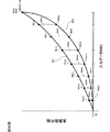
しかし、この方法では表示領域の明るさの調整はS段階でしか調整できない。点灯する表示領域のNを変化させた際の表示領域の明るさの変化を図31に示す。点灯走査線数Nの変化で明るさを調整するため、明るさの変化は図のように階段状になる。明るさの調整幅が小さい場合は問題が無いが、明るさの調整の幅が大きい場合、この調整方法ではNを変化させた際の明るさの変化が大きくなり、滑らかに明るさを変化させると言うことが難しくなる。
【0156】
そこで図6に示すようにゲートドライバ12内に二本の信号線62a、62bを配置する。この二本の信号線62a、62bはシフトレジスタに接続されているゲート制御用信号線64とOR回路65に接続される。OR回路65の出力は出力バッファ63に接続された後、ゲート信号線17に出力される。図28に示すようにゲート信号線17は信号線62と64がともにLOWのときのみ、LOWを出力し、どちらかがHIの場合はHIを出力する。
【0157】
これによりトランジスタ11b、11dがON状態(ゲート信号線17がLOW出力)の時に信号線62をHI出力にすることによりゲート信号線17をHI出力にすることができ、トランジスタ11b,11dをOFFにすることができる。尚、本発明は信号線とOR回路の組み合わせに限定するものではない。信号線62を変化させることによりゲート信号線17を変化させるもので、OR回路の代わりにAND回路、NAND回路、NOR回路を用いることも可能である。
【0158】
そして、図32に示すように信号線62bのHI出力期間を調整することによりEL素子15の発光時間を調整する。一つのEL素子15に注目した場合、点灯走査線数がNのとき、1フレーム間にN水平走査期間(H)点灯する。この時1水平期間(1H)内の信号線62bのHI出力期間をM(μ)とすると、1フレーム間の点灯時間はM×N(μ)減少する。図33にこの時の明るさの変化について示す。N=N´とN=N´−1(1≦N´≦S)の間の輝度は傾きが−M×N´で表現される。これにより、図31の階段状の明るさの変化はリニアな変化をすることが可能となる。
【0159】
この図では信号線62bは1Hに一回HI出力になるように書いてあるが、本発明はこれに限るものではない。数H期間に一度信号線62bがHIになるような処理方法も考えられ、またHI出力の期間は1H内のいかなる場所に配置しても問題はない。また、数フレーム間で明るさを調整することも可能である。例を挙げると2フレームに一回信号線62bをHI出力にするとHI出力の期間Mは見た目的には1/2になる。ただし、このような処理を行うとき特定の表示期間にのみ信号線62bをHI出力にすると画像表示領域に明るさのムラが出る可能性がある。
【0160】
このような場合、数フレーム間にわたって処理を行うことによって明るさのムラをなくすことができる。例えば図35に示すように奇数ラインの点灯時に信号線62bをHIにする表示方法351aと偶数ラインの点灯時に信号線62bをHIにする表示方法351bを1フレームごとに切り替える方法がある。これにより見た目には表示領域の明るさのムラは無くなる。本発明では表示領域の水平走査線数がS本あり、うちN本が転倒している場合、N/S≦1/4の場合にのみ信号線62を操作して明るさを調整する。最初にN/Sが1/4以下の時に信号線62を操作する利点について説明する。
【0161】
先に書いたように点灯水平走査線数Nの変化で明るさを調整すると明るさの変化は階段状になるためNが変化する境目で明るさが大きく変化することになる。表示領域の明るさが大きい場合、人間の視覚には変化の大きさに気づくにくいが、表示領域の明るさが小さい場合気づきやすくなる。そこで本発明では表示領域の明るさが小さい場合に信号線62を調整することにより明るさの変化量を微調整することが可能になる。
【0162】
次にN/Sが1/4以上の時の問題点について説明する。図9に示すようにソース信号線18とゲート信号線17bの間には浮遊容量91が存在する。信号線62bをHI出力にするとN本のゲート信号線17bが一斉にHI出力となるため、図36に示すようにソース信号線18とゲート信号線17bのカップリングによりソース信号線18が変化する。このカップリングにより蓄積容量19に正しい電圧を書き込むことができなくなる。特に図37に示すように低電流により書き込む低階調部においてはカップリングによる書き込み電圧の変化を補正することができずに371のように書き込み電圧が高くなる場合は低階調部が目的の明るさ373より高くなり、372のように書き込み電圧が低くなる場合は低階調部が目的の明るさ373より低くなる。
【0163】
以上により、明るさの変化を微調整できる利点を持ち、且つカップリングによる書き込み電圧の変化の影響が少ない期間としてN/S≦1/4が適当である。
【0164】
上記の駆動方法について図60に回路構成を示す。上記の駆動は601にて行う。上記駆動法はより細かい点灯率制御値を求めるため、552cより10bitのデータを出力し、点灯率制御値556を作成する。10bitのデータから点灯率制御値556を作成すると1024段階のデータが作成可能であり、8bitで点灯率制御値556を作成した場合の4倍の細かさで制御することが可能となる。しかし、点灯率は水平走査線数S段階でしか調整することができない。そこでSが8bitの値とすると生成された10bitの制御データの下位2bitを点灯率の微調整に使用する。もしくは前述図61のような駆動を行う場合、出力の際にLSB側にシフトされるnbit分のデータを点灯率の微調整に使用しても良い。
【0165】
本駆動は点灯率がN/S≦1/4の期間において行うことから555から601に点灯率制御値556を入力する。601は点灯率がN/S≦1/4において駆動を行う。先に示したとおり601から出力される信号線62bはゲートドライバ12から出力される信号線64bと論理演算を行い、その出力がゲート信号線17bとなっている。そのため、信号線62bの出力状況で全画素のトランジスタ11dを操作することが可能である。駆動を行わないN/S≧1/4の区間においては信号線64bの出力波形が17bに反映されるように信号線62bに出力する。
【0166】
N/S≦1/4の場合、601はHDに同期して駆動する。同期するのはHDだけとは限らない。601を駆動させるための専用の信号を設けても良い。601は入力される微調整用信号602とクロック(CLK)により、指定期間トランジスタ11dがOFFになるように信号線62bを操作する。先に示したようにNライン点灯している状況で1水平期間(1H)内の信号線62bのHI出力期間をM(μ)とすると、1フレーム間の点灯時間はM×N(μ)減少する。そのため、1Hの時間と602のデータを計算してMを算出し、62bの操作による点灯時間の減少を操作することにより、点灯率を滑らかに変化させることが可能となる。
【0167】
図60は図55に601を加えた形となっているが当然図58や図61などの本文に記載されたあらゆる回路構成に適用が可能である。
【0168】
次に図46に示す画素構成のアクティブマトリクス型表示装置において、ソース信号線からある画素に所定電流値を書き込む場合について考える。ソースドライバIC14の出力段から画素までの電流経路に関係する回路を抜き出した回路は図45(a)のようになる。
【0169】
階調に応じた電流IがソースドライバIC14内から、電流源452という形で引き込み電流として流れる。この電流はソース信号線18を通じて、画素16内部に取り込まれる。取り込まれた電流は駆動トランジスタ11aを流れる。つまり、選択された画素16においてEL電源線464から駆動トランジスタ11a、ソース信号線18を介して、ソースドライバIC36に電流Iが流れる。
【0170】
映像信号が変化して電流源452の電流値が変化すると、駆動トランジスタ11a及びソース信号線18に流れる電流も変化する。そのときソース信号線の電圧は駆動トランジスタ11aの電流−電圧特性に応じて変化する。駆動トランジスタ11aの電流電圧特性が図45(b)である場合、例えば電流源452が流す電流値がI2からI1に変化したとすると、ソース信号線の電圧はV2からV1に変化することになる。この電圧の変化は電流源452の電流によっておこる。
【0171】
ソース信号線18には浮遊容量451が存在する。V2からV1までソース信号線電圧を変化させるにはこの浮遊容量の電荷を引き抜く必要がある。この引き抜きにかかる時間ΔTは、ΔQ(浮遊容量の電荷)=I(ソース信号線に流れる電流)×ΔT=C(浮遊容量値)×ΔVとなる。ここでΔV(白表示時から黒表示時間の信号線振幅)は5[V]、C=10pF、I=10nAとすると、ΔT=50ミリ秒必要となる。これはQCIF+サイズ(画素数176×220)を60Hzのフレーム周波数で駆動させるときの、1水平走査期間(75μ秒)よりもながくなるため、仮に、白表示画素の下の画素に黒表示を行おうとすると、ソース信号線電流が変化途中に画素に電流を書き込むためのスイッチトランジスタ11a、11bが閉じてしまうため、中間調が画素にメモリーされることにより白と黒の中間の輝度で画素が光ってしまうことを意味する。
【0172】
階調が低くなるほどIの値が小さくなるため、浮遊容量451の電荷を引き抜きにくくなるため、所定輝度に変化する前の信号が画素内部に書き込まれてしまうという問題は、低階調表示ほど顕著に現れる。極端にいうと黒表示時は電流源452の電流は0であり、電流を流さずに浮遊容量451の電荷を引き抜くことは不可能である。
【0173】
そこでこの問題を解決するために、図47に示すようなソース信号線18に通常のn倍の電流を通常の1/n時間印加するn倍パルス駆動を使用する。この駆動法により通常よりも高い電流を書けることによりコンデンサへの書きこみ時間を短縮できる。ソース信号線にn倍の電流を流すと有機EL素子にもn倍の電流が流れるため、ゲート制御信号を483aとなるように出力しTFT11dの導通時間を1/nにすることにより、有機EL素子15に1/nの期間だけ電流を印加し平均印加電流は変化しないようにする。
【0174】
ソース信号線18の電流値変化に要する時間tは浮遊容量451の大きさをC、ソース信号線18の電圧をV、ソース信号線18に流れる電流をIとするとt=C・V/Iであるため電流値を10倍大きくできることは電流値変化に要する時間が10分の1近くまで短くできる。またはソース線の浮遊容量451が10倍になっても所定の電流値に変化できるということを示す。従って、短い水平走査期間内に所定の電流値を書きこむためには電流値を増加させることが有効である。
【0175】
入力電流を10倍にすると出力電流も10倍となり、ELの輝度が10倍となるため所定の輝度を得るために、図1のTFT11dの導通期間を従来の10分の1とし、点灯率を10分の1とすることで、所定輝度を表示するようにした。
【0176】
つまり、ソース信号線18の浮遊容量(寄生容量)451の充放電を十分に行い、所定の電流値を画素のTFT11aにプログラムを行うためには、ソース信号線18から比較的大きな電流を出力する必要がある。しかし、このように大きな電流をソース信号線18に流すとこの電流値が画素にプログラムされてしまい、所定の電流に対し大きな電流がEL素子15に流れる。たとえば、10倍の電流でプログラムすれば、当然、10倍の電流がEL素子15に流れ、EL素子15は10倍の輝度で発光する。所定の発光輝度にするためには、EL素子15に流れる時間を1/10にすればよい。このように駆動することにより、ソース信号線18の寄生容量を十分に充放電できるし、所定の発光輝度を得ることができる。
【0177】
なお、10倍の電流値を画素のTFT11a(正確にはコンデンサ19の端子電圧を設定している)に書き込み、EL素子15のオン時間を1/10にするとしたがこれは一例である。場合によっては、10倍の電流値を画素のTFT11aに書き込み、EL素子15のオン時間を1/5にしてもよい。逆に10倍の電流値を画素のTFT11aに書き込み、EL素子15のオン時間を2倍にする場合もある。
【0178】
このN倍駆動を使用するとソース信号線に流れる電流量を増やすことができるため、所定輝度に変化する前の信号が画素内部に書き込まれてしまうという問題を解決することができる。たとえば、ゲート信号線17bは従来導通期間が1F(電流プログラム時間を0とした時、通常プログラム時間は1Hであり、EL表示装置の画素行数は少なくとも100行以上であるので、1Fとしても誤差は1%以下である)とし、N=10とするとすれば、最も変化に時間のかかる階調0から階調1へもソース容量が20pF程度であれば75μ秒程度で変化できる。これは、2型程度のEL表示装置であればフレーム周波数が60Hzで駆動できることを示している。
【0179】
更に大型の表示装置で浮遊容量(ソース容量)451が大きくなる場合はソース電流を10倍以上にしてやればよい。一般にソース電流値をN倍にした場合、ゲート信号線17b(TFT11d)の導通期間を1F/Nとすればよい。これによりテレビ、モニター用の表示装置などにも適用が可能である。
しかし、N倍駆動は、同じ明るさで表示しても画素に瞬間的に流れる電流がN倍になるため、有機EL素子に大きな負担がかかる。
【0180】
そこで、本発明の入力データに応じて点灯率を制御する駆動方法を用いて表示画像の低輝度部において点灯率とともにソース信号線18に流す電流量を制御して図49に示すような低輝度部でのみN倍パルス駆動をすることを提案する。この駆動方法のメリットは、前述の電流量不足の問題は高輝度部では起こり難いため、有機EL素子に負担のかかるN倍パルス駆動は高輝度部では行わず、全体的に画素に流れる電流が少ない低輝度部においてのみN倍パルス駆動を行うことにより、有機EL素子の負担を軽くしつつ、前述のソース信号線の浮遊容量451のために所定輝度に変化する前の信号が画素内部に書き込まれてしまうという問題を解決できることにある。
【0181】
具体的には低輝度部では点灯率を1/N1にして、それに応じて総電流量が目的の値になるように ソース信号線に流す電流N2倍に増やす。この際、N1=N2である必要はない。N1≦N2の場合もあるし、N1≧N2の場合ももちろんある。ただし、本駆動の目的はソース信号線18に流す電流量を増やすことにあるのでN2>1である。そして点灯率は必ずしも下げなければいけないと言う訳ではない。求める入力データに対する有機ELパネルに流れる電流量の関係によっては点灯率を変えないことや、点灯率の上昇を抑えると言う処理をすることもある。
【0182】
仮に入力データと点灯率の関係を図50のように入力データが30%未満の領域では点灯率を最大にし、30%以上の領域では有機ELパネルに流れる電流量がバッテリー241の限界容量を超えないように点灯率を下げて行くような駆動を考える。そして前述の駆動時において入力データが30%未満の領域においてN倍パルス駆動を行うとする。つまり、白色を表示するのに相当する電流量を100と表現する場合に、所定の電流量が30以下で表される低電流領域の階調については、N1>1、N2>0でかつN1≧N2であるような正の数を係数都市、所定の電流量をW、そのときの電流値をIorg、発光期間をTorgとすれば、電流値はIorg×N1、発光期間はTorg×1/N2を満たす電流量を所定の電流量に替えて印加するわけである。ただし、このN倍パルスと、通常駆動の切り替え点は30%に固定するものではない。しかし、寿命を考えると30%以下の領域にN倍パルスとの切り替え点を持つことが好ましい。
【0183】
ここでN倍パルス駆動のやり方について2通り提案する。一つ目に511のように入力データが30%未満の領域では点灯率を1/Nにし、ソース信号線に流す電流量をN倍にする方法がある。二つ目は512のように入力データが30%の状態から0%にかけて徐々に点灯率を下げ、逆にソース信号線に流す電流量を徐々に上げて行く方法がある。ともに有機ELパネルが流す電流量は図50の関係になるが一つ目の方法は入力データが30%未満の状況では点灯率も電流値も固定で良いため、回路作成が非常に容易であると言うメリットがある。しかし、入力データが30%の境目で点灯率と電流値が同時に大きく変わるので変わる瞬間にちらつきが見えてしまうと言う問題も有している。
【0184】
二つ目の方法は入力データが30%未満の状況では点灯率と電流値を同時に操作しなければならないので回路作成が複雑になると言うデメリットがある。しかし、この方法だと点灯率と電流値は緩やかに変化させることが可能であるのでちらつき等の問題点がない。さらに前に示したように所定輝度に変化する前の信号が画素内部に書き込まれてしまうという問題はソース信号線に流す電流量が少なければ少ないほど顕著に出るものなので入力データが減少に応じてソース信号線に流す電流量をふやすと言う方法は理にかなっているし、有機EL素子に対する負担も小さくなる。この方法により、極力有機EL素子への負担を小さくし、かつ所定輝度に変化する前の信号が画素内部に書き込まれてしまうという問題を解決する駆動方法を実現した。
【0185】
図64にて本駆動の回路構成について説明する。552で加算された映像データは基準電流制御モジュール641に入力される。641では入力されたデータに応じて、ソース信号線18に流れる電流量を増減させるようにソースドライバー14を制御する。
【0186】
図62・図63にてソースドライバー14について説明する。図63に示すようにソースドライバー14は基準電流629に応じてソース信号線18に電流を流す。さらに基準電流629について説明すると図62において基準電流629は節点620の電位と、抵抗素子621の抵抗値により決まる。さらに節点620の電位は電圧調節部625により、制御データ信号線628により変化させることが可能である。つまり制御データ信号線628を641により制御すれば、抵抗素子621の抵抗値によって決められた範囲内で変化させることが可能となる。
【0187】
上記の駆動法の適用例として図65にて図61の回路構成に上記の駆動法を付加した回路構成を示す。入力データと点灯率、基準電流値の関係が512のようになる場合、基準電流を変化させる領域を513と変化させない領域514で区別する。入力データが513の領域にある場合図65のx_flagが1になり、514の領域の場合、0になるように構成する。また、同じようにそのフレームでの点灯率Y(t)が513にある場合はy_flagが1になり、514の場合は0になる。すなわち、y_flagが1の場合は基準電流を変化させている領域となり、651にてy_flagが1のとき556のデータに応じて基準電流の制御データ信号線628を変化させる。650内はy_flagとx_flagの組み合わせで構成されている。y_flagとx_flagがともに0のときはともに514の領域にいるため、Y´(t)は555と同様のシーケンスで設計すれば良い。同じようにy_flagとx_flagがともに1のときは513の領域内で動くため、基準電流は変化するが点灯率の計算に関しては555と同様のシーケンスでよい。y_flagとx_flagが(0,1)もしくは(1、0)のときは513の領域から514の領域に移ろうとしている状態(もしくは逆)である。513の領域では点灯率と基準電流値がともに変化するが、かけあわせると常に一定になるように動いている。つまりは514における点灯率を最大の状況(D_MAXと定義する)と同じものと言って良い。そこでy_flagが0でとx_flagが1の状態、すなわち514の領域から513の領域に移動する時はY´(t)をD_MAXとする。逆にy_flagが1でとx_flagが0の状態、すなわち513の領域から514の領域に移動する時はD_MAXから555で導かれるY´(t)に向けて移動すると考えるとY(t)を保持しているレジスタ583にD_MAXを入力し、Y´(t)を555と同様のシーケンスで設計することにより違和感のない点灯率の変化を実現することができる。
【0188】
また、図30のような点灯率のカーブを描く方法と併用する回路構成について説明する。この駆動方法は図30のような点灯率のカーブを描く方法と併用することにより、回路規模を小さくすることが可能になる。
【0189】
図130に示すように、入力データを2のS乗で分割し、2のn乗の入力データまでN倍電流値、1/N点灯率駆動を行うとする。最大の点灯率の値をa、通常の点灯率抑制駆動の最小点灯値をb、N倍電流値、1/N点灯率駆動の最小点灯率の値をcとし、また入力データが0、つまり最小値から2のn乗までをCASE1、2のn乗から2の(n+1)乗までをCASE2、2の(n+1)乗から2のS乗、つまり最大値までをCASE3とする。また、CASE1のときだけ1になるFLAG_AとCASE3のときだけ0になるFLAG_Bを用意する。これによりCASE1は(FLAG_A,FLAG_B)=(1,1)、CASE2は(FLAG_A,FLAG_B)=(0,1)、CASE3は(FLAG_A,FLAG_B)=(0,0)と表すことができる。続いて、図131にてこの駆動を実現する回路構成を示す。FLAG_AとFLAG_Bの値の判別は入力データをシフトレジスタによりシフトさせて比較器に入力すればわかる。nビットシフトさせたデータが0だったらFLAG_Aは1、それ以外は0、さらに1ビット(計n+1ビット)シフトさせて0だった場合、FLAG_Bは1、それ以外は0である。尚、FLAG_AとFLAG_Bの0と1は逆でもかまわない。この二つのフラグを利用して、CASE1から3を満たす回路を作成する。
【0190】
3つの式は点灯率をY、データをX(最大2のS乗)とすると次のように表される。
CASE1・・・Y=((a−c)/2n)・X + c
CASE2・・・Y=a−2・((a−b)/2S)・X + 2n・((a−b)/2(S−1))
CASE3・・・Y=a−((a−b)/2S)・X
この3つを実現するにはそれぞれの場合において演算を行えばよいが、回路構成において演算処理は回路規模が大きくなるため、できるだけ演算を行う回数を減らすことが好ましい。特に乗算処理は回路規模に大きな負担をかける。そのため、セレクター回路とシフトレジスタを多用することにより負荷の少ない回路構成を実現する。
【0191】
まずa−b、a−cをそれぞれ行う。その値をセレクター1311にかける。上の式からCASE1の場合のみa−cを行うのでFLAG_Aが1のときa−cを出力し、0のときはa−bを出力する。セレクター1311の出力値と入力データXの演算を行う。これにより、(a−b)・Xの値と(a−c)・Xの値が完成する。CASE2とCASE3では傾きが2倍であるため、セレクター1311の出力値をそのままのものと2倍したものをFLAG_Bの値によりセレクター13212で選択する。この際に2倍する方法としてはセレクター1311の出力値をMSB側に1ビットシフトする方法と、シフトレジスタを使用しなくても二つとも2Sで割っているのでセレクター1311の出力値の下位Sビットを削ったものとS−1ビット削ったものをセレクター1312にかければよい。aとセレクター1312の出力の減算結果はCASE3のYの値と一致する。CASE2はこの演算結果に2n・((a−b)/2(S−1))を加えたものである。また、CASE1はcに((a−c)/2n)・Xを加えたものと考えることができるのでこの出力値とcの値をFLAG_Aで選択されるセレクター1313にかけることにより、あとはセレクター1313に加える値をセレクトすることで点灯率を求めることができる。2n・((a−b)/2(S−1))は((a−b)/2(S−1))をnビットMSB側にシフトさせたものである。また((a−c)/2n)・Xは(a−c)・X、即ちセレクター1311の出力と入力データXとの演算値をnビットLSB側にシフトさせたものである。ともにnビットシフトさせるのでカウンター1314一つでシフトを完了させることができる。2n・((a−b)/2(S−1))はa−bの値をnビットMSB側にシフトさせた後下位S−1ビットをけずって出力する。この二つの出力をセレクター1315にかける。このセレクターはCASE1とCASE2のセレクターであるのでFLAG_Aを使用する。CASE3の場合はこの出力を足す必要がないため、FLAG_Bでセレクター1316にかけ、CASE3の場合は0を出力するようにする。これにより、最小限の演算とセレクターによりすべてのCASEの点灯率の算出が可能になる。
この方式はCASE1から3を別々に演算するのに比べると回路規模は半分以下になり、この仕組みを実現するのに非常に効果が高い。
【0192】
一般に画像はガンマカーブを用いている。ガンマカーブとは低階調部を抑えることにより、全体的にコントラスト感がでるような画像処理である。しかし、ガンマカーブにより低階調部が抑えられると、低階調部が多い画像では黒く潰れてしまい奥行き感のない画像になってしまう。とは言え、ガンマカーブを使用しないと高階調部が多い画像ではコントラスト感が出ない画像になってしまう。
【0193】
本発明の点灯率制御駆動を行う場合、表示領域に低階調表示が多い場合は点灯率を上げることにより、全体が明るくなる。この時、ガンマカーブにより低階調部をつぶしていると表示される画素と表示されない画素の明るさの差が大きくなるため、より奥行きのない画像になる可能性がある。また、表示領域に高階調表示が多い場合は点灯率を下げるため、表示画素と非表示画素の明るさの差が小さくなる。そのため、ガンマカーブで画像をつぶさないとコントラスト感のない画像になってしまう。
【0194】
そこで本発明の電流量制御駆動と連動させて表示領域の変化により、ガンマカーブを制御する駆動方法を提案する。
【0195】
図67・図68にてγカーブを実現する回路構成について説明する。入力される色データをグラフの横軸にとり2のn乗で分割する。図67では8分割し、それぞれを671a、671b・・・671fとしている。そして、671a〜fの境目に対応するγカーブの値672a〜fを入力する。図68では入力される色データは8bitと仮定して処理を行っている。最初に681にて入力データ680の上位3bitを判定する。ガンマカーブは8分割(2の3乗分割)されているので680の上位3bitの値により、入力データ680は671a〜fのどの領域にいるか判断することができる。仮に671cの領域に680がいるとする。671cの領域はガンマカーブの値が最低が672b、最高が672cであり、256段階の入力データを8分割しているので1区間は32段階に分けられる。よって671cのグラフの傾きは(672b−672c)/32となる。入力データが671cの領域のどの場所にいるかは680の下位5bitの値と等しいので(680の下位5bit)×(672b−672c)の値をLSB側に5bitシフト(32での除算)したものが671c内での増加分となる。すなわち、上記に672bの値を加えたものが入力データ680がガンマカーブにより変換された出力値682となる。
【0196】
続いて図66・図69にて552内で作られた有機ELパネルの表示状態などを示したデータ557を用いて、表示状態によりγカーブを調整する回路構成について説明する。まず691にて2種類のγカーブを作成するため、661a〜661h、662a〜662hの値を決める。ここでは661≧662が成り立っているものとする。γカーブは使用するデバイスによっても違うのでこの値は外部から設定できるようにするべきである。そして661a〜fと662a〜fの各差663a〜fをとる。その後、691から692に対して661a〜fと663a〜fを出力する。692には552から出力された表示状態のデータである557も入力される。692では557に応じてγカーブの値を決める。557が大きいほど、画像は高階調が多く、ガンマカーブをきつくして画像にメリハリをつける必要があり、557が小さいほど画像は低階調部が多く、ガンマカーブを緩くして奥行きのある映像を作る必要がある。557は0〜255のデータであることから(661a〜fのデータ)−{(663a〜fのデータ)×(557のデータ/255)}と言う演算により557に応じたガンマデータ693a〜fが作成される。このガンマデータ693a〜fを683に入力する。683は図68で説明したように、入力される色データ680から672a〜fのデータに基づいて作られたガンマカーブにより変換されたデータが出力されるモジュールである。672a〜fに693a〜fが入力され、入力されるRGBのデータ695が693a〜fによって作られるガンマカーブにより変換され出力696としてソースドライバー14に入力される。
【0197】
上記の説明では緩やかなガンマカーブ661から557に対応したデータを減算すると言う方式をとっているが、当然のことながらきついガンマカーブ662から557に対応したデータを加算すると言う方法をとっても良い。
【0198】
また、ガンマカーブは2種類からつくるのに限るものではない。複数のガンマカーブから表示映像に合わせたガンマカーブを作る構造を用いてもよい。
【0199】
ガンマカーブの変化も点灯率の変化と同様、頻繁に変化させるとちらつきが見えると言う問題を有している。そこで点灯率の変化を612により遅延させたのと同様に557も612により変化の速度を遅延させてやることは非常に有効である。
【0200】
図ではRGBを694で同様に処理しているが、RGBを別別にやることにより、RGB個別のガンマカーブを作ることも可能である。
【0201】
以上の駆動により、表示領域に低階調部が多い場合はガンマカーブを緩くすることにより奥行き感を出し、高階調部が多い場合はガンマカーブをきつくすることにより、コントラスト感をだすような駆動を行うことができる。
【0202】
また、RGBを独立してガンマカーブを作成する手段として図129に示すように作成されたガンマカーブ672にRGBそれぞれに補正値1291a〜1291fを加えることによってRGBを別々にガンマカーブを作ることが可能となる。この方式は複雑なガンマカーブの演算は1種類で済むため、回路規模を大きくせずに実現が可能となる。
【0203】
有機EL素子15は劣化するため、固定パターンを表示し続けると一部の画素の有機EL素子15のみが劣化して、表示していたパターンが焼きつく場合がある。焼きつきを防ぐためには表示している映像が静止画かどうか判別してやる必要がある。
【0204】
静止画を判別する方法としてはまず、フレームメモリを内蔵し、1F期間のデータを全てフレームメモリに記憶させることで次フレームとの映像データの正否を判断し、静止画かどうか判断させる方法がある。この方法は確実に映像データの違いを認識できると言う利点を有しているがフレームメモリを内蔵しなくてはならないため、回路規模が非常に大きくなってしまう。
【0205】
そこで図71に示すようにフレームメモリを使わずに静止画かどうか判断する方法について提案する。判断する方法として、1F期間の全画素のデータを加算した合計値で判断する方法がある。映像がかわらない場合、映像データも変わらないのでデータの総和量はかわらない。そのため、1F内の全データを加算し、比較することで静止画かどうか検出することができる。この方法だと全映像データをそのまま記憶させるよりも非常に少ない回路規模で実現できる。しかし、データの総和量をとる方法は特定のパターンにおいて効果をなさない場合がある。例えば、黒い画面の中を白いブロックが飛びまわるような画像の場合、白いブロックの位置は違ってもデータの総和量としては同じのため、静止画として誤認識してしまうことになる。そこで本発明では数個の画素を組み合わせてデータを作ることにより、他の画素のデータとの相関関係を持たせる方法を提案する。
【0206】
まず、711はデータイネーブル(DE)とクロック(CLK)によって動作する。これは常にデータが来ているわけではなく、必要なデータでのみ判定を行うためのものである。
【0207】
図70に示すように6bitの映像データ701a,701bが入力される場合、8bitのレジスタ702を用意し、奇数bitと偶数bitにそれぞれの映像データの上位4bitを入力し、一つのレジスタを構成する。この時、レジスタ702は8bitである必要はない。回路規模は大きくなるが12bitのレジスタを持っても良いし、精度が落ちて良いならば8bit未満のレジスタ構成にしても良い。また、2つ映像データの比率を変えても良い。8bitのレジスタに入力する場合、701aから5bit、701bから3bitと言う割合にしても良い。更にレジスタに入力するデータは必ずしも上位から取る必要はない。下位4bitを選択して入力しても良いし、カウンター713の値に応じて取る場所を変えることも有効な手段である。図70に示すように2画素で見た場合、703の場合はどちらのパターンもデータは同じになるが、704の場合はデータが違うようになるため、静止画として誤認識しない。図70と図71は駆動方法を簡略化して説明するために2画素間で相関関係を持たしているが、これは3画素以上でも構わない。多くの画素で図70の方式を行うと、より静止画検出の精度が上がるメリットを有しているがレジスタ702のbit数が大きくなるため、回路規模が大きくなるデメリットも有している。そのため、図74に示すようにbit数の違う数種類のレジスタを用意し、複数の画素で相関関係を持たせる方法もある。
【0208】
712ではレジスタのデータとカウンタ713の値で論理演算を行った値を加算している。カウンタ713は水平同期信号(HD)によってリセットされ、クロックによってカウントアップするモジュールである。そのため、表示領域の水平方向の座標を示しているのと同じであり、このカウンタとデータを論理演算することにより、データに水平方向の座標の重みをつけることが可能である。
【0209】
714では1水平期間分のデータとカウンタ715の値で論理演算を行った値を加算している。カウンタ715は垂直同期信号(VD)によってリセットされ、HDによってカウントアップするモジュールである。そのため、表示領域の垂直方向の座標を示しているのと同じであり、このカウンタとデータを論理演算することにより、データに垂直方向の座標の重みをつけることが可能である。
【0210】
以上の方式を利用することにより、静止画検出の精度を高めることが可能である。しかし、必ずしも上記の方法を全て使用する必要はない。上記の方法はより精度を高める手法であり、上記の方法を全て使用しないと静止画を検出できないわけではない。
【0211】
上記の方法を組み合わせた形により、フレームデータ716が出来る。フレームデータは前フレームのデータ717と718にて比較を行う。718で行う比較の方法としては二つのデータが必ずしも同じである必要はない。映像データには少なからずノイズが乗るものである。そのため、ノイズが全く無いデータでない限り二つのデータが同じであることは無い。718では必要精度により、二つのデータの誤差範囲を決めてやるのがよい。比較方法として、二つのデータを減算して演算結果から静止画かどうか判断する方法がある他、フレームのはじめに前フレームのデータ717を反転させてフレームデータ(レジスタ)716に入力させて、1F間に加算されたフレームデータ716がいかに0に近づくかにより静止画を判断する方法もある。712、714は加算器を使用しているが前フレームのデータ717から減算器を用いていかに0に近づくかで静止画かどうか判断する方法もある。
【0212】
図71では表示領域全てのデータを加算することにより、静止画かどうか判断している。しかし、表示画像によっては50%が静止画で残り50%が動画と言う場合もありえる。そのため、カウンタ713とカウンタ715により、画面を複数に分割して画面内のどの範囲が静止画かどうか判断して様々な処理を行う方法も有効である。
【0213】
比較器718が静止画と判断した場合、カウンタ719をカウントアップする。逆に動画と判断した場合はカウンタ719をリセットする。つまりカウンタ719の値が静止画が続いている期間と言うことになる。
【0214】
まず、このカウンタ719を利用して、EL素子15の劣化速度を落とすために点灯率を落とす方法を提案する。
【0215】
カウンタ719がある値になった時点で信号線7101を操作する。この信号線7101はHIのときに点灯率を強制的に制御する信号線である。710内で点灯率制御値556と信号線7101がつながるモジュールを用意し、信号線7101がHIの場合、強制的に点灯率を現在の1/2に落とすように回路構成する。このとき強制的に点灯率を落とす値は1/2に固定する必要は無く、必要に応じて点灯率を減少させるようにする。点灯率が減少するため、有機EL素子15は発光量が減少し、寿命劣化の速度を落とすことが可能である。もちろん、7101がLOWのときに点灯率を落とすように制御しても構わない。
【0216】
しかし、劣化速度を上記の方法で落としても長時間流していれば焼きつきは起きてしまう。そのため、長時間静止画状況が続いた場合、有機EL素子15に流す電流を完全に止めてやる必要がある。そのために信号線7102を用いて信号線62bを強制的に操作して、強制的に有機EL素子に電流を流す期間を制御するスイッチング素子をOFFにして有機EL素子に電流が流れるのを阻止する。信号線62bは先に示したとおり、スイッチング素子11dを操作するゲート信号線17bを強制的にHI,LOWどちらかに固定することができる信号線であり、これを信号線7102で制御することにより、長時間静止画が続いた場合に有機EL素子の発光を止めることが出来るため有機EL素子の焼きつきを防ぐことが可能となる。
【0217】
更に有機EL素子を利用した表示装置では静止画を検出できることにメリットがある。左記に示したように有機EL素子は間欠駆動を行うことが可能であり、本発明でも点灯率制御値を制御することにより、点灯率を制御している。先に示したように間欠駆動において、黒を一括で挿入することにより、映像の輪郭をはっきりさせることが可能となり、画像が非常に良好となる。しかし、黒を一括で挿入することはデメリットも有している。挿入する黒領域が大きくなれば大きくなるほど、人間の目が黒挿入に追いつくことが可能となり、黒挿入がちらつきとして見えてしまうと言う問題がある。これは主に静止画でよく見られる問題であり、動画の場合、映像の変化により、黒挿入のちらつきは見えない。黒を分割して挿入するとこの現象は改善されるが、同時に黒一括挿入によって輪郭をはっきり表示させると言う効果は使えないことになる。
【0218】
そこで図72に示すように動画表示の場合、黒を一括で挿入する駆動方法を行い、静止を検出すると黒を分割して挿入することにより、静止画時のちらつきを防止する駆動方法について提案する。
【0219】
図73にてカウンター554と点灯率制御値を利用して黒を分割して挿入するための回路構成について説明する。先に示したようにスイッチングトランジスタ11dはゲート信号線17bによって制御され、ゲート信号線17bはゲートドライバ12に入力されるST2によって決まる。図75に示すようにST2が1H単位でON/OFFを繰り返すと、スイッチングトランジスタ11dは1HごとにON/OFFを繰り返し、722のように黒が分割されて挿入されるような画像となる。そこで、731のようなセレクタを多数使用して黒の分割挿入を実現する。
【0220】
710の回路構成はまず最初にカウンタ554のLSBに注目する。セレクタ731は入力値Sが1のときにBの値を、0のときはAの値を出力する。すなわち731aで考えるとカウンタ554のLSBの値が1のときは点灯率制御値のMSBの値を出力する。カウンタ554のLSBが0のときは731bの出力値が反映される。731bはカウンタ554の下位から2bit目が1のときに点灯率制御値の値が8bitの場合、7bit目の値が出力される。これを3bit目、4bit目・・・と繰り返して行く回路構成になっている。カウンタ554のLSBは1H毎にHI,LOWを繰り返す。点灯率制御値が8bitの場合、8bit目が1のときは128以上であるため、2Hに一回は必ずHIになる。すなわち、カウンタ554のLSBをセレクタのスイッチにしてLSBが1のときに点灯率制御値のMSBの値を出力すると、2Hに一回ST2がHIになる。LSBが0の場合は一つ左のセレクタからでる信号の値がST2に出力される。そしてカウンタ554のLSBが0でカウンタ554の下位から2bit目が1のときに点灯率制御値の7bit目が出力されることになる。つまり点灯率制御値の7bit目が出力されるのは4Hに1回と言うことになる。同様に続けて行くと点灯率制御値の6bit目の値が出力されるのは8Hに1回・・・と言う形になり。これをくみあわせることにより、黒一括挿入から黒分割挿入に変換させることが可能となる。
【0221】
上記の黒分割挿入の回路構成と、先に示したフレームメモリを使用する方法を含めて、静止画を検出する回路方法を組み合わせることにより、動画では黒を一括挿入して輪郭をはっきりさせる駆動方法を行い、静止画では黒を分割して挿入することにより一括挿入によるちらつきを防止する駆動を実現することができる。
【0222】
先に示したソース信号線18の浮遊容量451を引きぬく手段としてインピーダンスの低い電圧源773を用意しソース信号線18に電圧を印加する方法がある。上記の手法をプリチャージ駆動と呼ぶものとする。
【0223】
プリチャージ駆動の回路構成を図77に示す。回路内に電圧源773と電圧印加手段775を設ける。電圧印加手段775がスイッチ776をONにすると電圧源773がソース信号線18の浮遊容量451を充放電する。図面の都合上774はソースドライバー14とは別に書いているが、774はソースドライバー14に内蔵しても良い。また、電圧印加手段775によってプリチャージを行うソース信号線18を選択することを可能にする回路構成にすると、画素単位でプリチャージのON/OFFを調整できるので細かい設定が可能となる。
【0224】
本発明では上記の回路構成に静止画検出手段711を使用する。これは711の変わりにフレームメモリなどを用いても構わない。動画に比べて静止画の方が先に示した浮遊容量451による画像劣化が目立つ。よって711により静止画を検出し、比較器772により電圧印加手段775を操作し、プリチャージを行うことにより、静止画時の画像劣化を防ぐことができる。
【0225】
前記のように動画を表示する場合に輪郭をはっきりさせる為に黒を一括挿入するのが好ましいのに加えて、有機EL表示装置を駆動させるゲートドライバー回路の電力面からしても黒は一括で挿入する方が好ましい。
【0226】
また、EL表示パネルを駆動させるゲートドライバー12はスタートパルスST2をクロックCLK2で動作するシフトレジスタ61bにより、各ゲート信号線17bを動作させる。781に示すように黒を一括で挿入する場合、1フレーム間に各ゲート信号線17は1回ずつONとOFFをするだけで良い。しかし782のように黒を分割して挿入する場合、ゲート信号線17は繰り返しONとOFFをすることとなる。このため、複数の信号線を同時にON・OFFすることになりゲートドライバー12の消費電力が大きくなると言う問題点がある。
【0227】
以上の観点から、有機EL表示装置は通常は黒を一括で挿入する方が好ましい。しかし、黒を一括で挿入する場合静止画において黒を一括で挿入することによるちらつきが見える。そのために静止画、もしくは動きの少ない映像を表示している。本発明搭載パネルの表示状態の説明図である。本発明搭載パネルの表示状態の説明図である。この場合、黒を一括挿入から分割挿入に変化させる仕組みが必要となる。しかし、黒を一括挿入から分割挿入に変えると切り替わりの瞬間にちらつきが見える。これには二つの理由が考えられる。
【0228】
一つ目の理由は分割挿入への切り替え時の一時的な輝度の劣化が考えられる。
【0229】
図79に示すようにP本の水平走査線の内、S本の水平走査線が点灯している状況を考える。この時の点灯していない、つまり黒の走査線数はP−S(本)である。これを2分割させる場合、点灯していない走査線数は(P−S)/2(本)ずつになる。切り替わる前は常にS本の走査線が点灯している状況だが、切り替わりの瞬間のみS/2(本)点灯してから(P−S)/2(本)の間、点灯走査線数がS/2になる。この間、表示領域の輝度はS/2になるため、わずか1フレーム内ではあるが輝度減少が発生し、それが画像劣化になっていると考えられる。
【0230】
二つ目の理由は黒の間隔の急激な変化が考えられる。
【0231】
黒を一括で挿入すると画像劣化する原因の一つとして、人間の目が無意識に挿入される黒を追っていることが考えられる。そこで黒を一括で挿入している状態から黒を分割して挿入することで、急激に画像が変わったような間隔を覚え、画像劣化のように感じると考えられる。
【0232】
本発明では以上の二つの問題点を解決し、画像の劣化無く、黒の挿入方法を一括挿入から分割挿入に変化させる方法を提案する。切り替え時に画像の劣化が起こるのは前述のように輝度と黒の感覚の急激な変化であるため、本発明では図89に示すように黒の間隔を複数のフレーム間にかけて徐々に分割して行く方法により、切り替え時の画像の劣化を防ぐ。図80はN水平走査期間(以後、水平走査期間はHと表記する)分の間隔を作って点灯水平走査線数を2分割した場合の輝度の変化を示している。S本の水平走査線を点灯させている状況において2分割したスタートパルスの前段を801とし、後段を802とすると801と802の点灯水平走査線数はS/2となる(S=2・4・6…・)。このため、前段のスタートパルス801がゲート信号線に出力された後、S/2(H)の間、EL表示パネルの点灯している水平走査線数pは(S/2)−N本である。その間の表示パネルの輝度は切り替え前に対して
(p/S)× 100 (%) ・・・ (6)
となる。図81に示したグラフは一度に図79と図80においてN=1で分割した場合の輝度差をグラフで表現したものである。この分割時の輝度が画像劣化に大きく関わっていると考えられる。
【0233】
式(6)の値はp=S−Nのため図100に示すようにSとNによって変化する。実測値より式(6)の値が75%未満になると画像の劣化が起こることが解析できた。そのため、本発明では式(6)の値が75%以上となるNの値、つまり式(6)よりN≦S/4(ただしN≧1)ずつ黒の挿入間隔を広げて行く方法を提案する。式(6)の値が75%以上であれば画像劣化は起こらないが、80%以上であれば、更に効果が期待できる。最も好ましくは90%以上(N≦S/10)がよい。
【0234】
ただし、本発明では輝度が75%未満にならなければ、どのような変化をさせても構わない。図79ではS本の水平走査線が点灯している状態から点灯水平走査線数を2分割する場合に、S/2にしているがこれをS´本とS−S´本に分割しても構わない(S´<S)。また、一度に分割する量は2分割に限るものではない。仮にN=3であるとすると、1水平走査期間ずつの間隔をあけると一度に4分割しても輝度は90%以上を保つことが可能であるため、処理に影響はない。図82では黒の挿入間隔を一定にする為、黒の挿入間隔が同じになる場所まで点灯間隔を制御した後に次の分割へと移っている。しかし、図83に示すように先に分割してから黒の挿入間隔を調整しても構わない。また、点灯間隔はそろえた方が画像劣化の改善効果が高いが必ずしもそろえる必要はない。
【0235】
前記の方法は黒の挿入間隔を徐々に広げて行く方式であるが、図84のように逆に点灯水平走査線数を徐々に減らして行くやり方でも良い。S本点灯している状況からS−N本とN本に分割し、次はS−2N本と2N本に分割すると言う方法で点灯させると、輝度は90%未満にはならないため、輝度の変化による画像劣化は起こらない。この方法は画像劣化の二つ目の理由である黒の挿入間隔の急激な変化を起こしてしまうため、画像劣化が起こると考えられる。しかし前述の通り、輝度の変化による画像劣化は解決できる為、効果がある。
【0236】
図85に本発明の駆動方法を実現する回路構成図を示す。本発明の回路構成は二つのカウンター回路851、852、その二つのカウンターから信号を生成する回路853、854とその二つのカウンターの加算値を制御する加算値制御回路855、そして853から出力される出力856と854から出力される出力857のどちらかを出力するセレクター858により構成される。
【0237】
回路854は図73に示した点灯率制御値とカウンター554の値から波形を分割して出力する回路をより遅延の少ない回路に構成しなおしたものである。図73の回路と854は同じものであり、どちらを使用しても構わない。回路853はカウンター851が0のときに出力856をHIにする。また、加算値制御回路855内で、点灯率制御値から出力856をLOWにするカウンター値を生成する。点灯率制御値がNビットであり、ゲートドライバー12に入力するスタートパルスST2を2のt乗に分割する場合、点灯率制御値の上位(N−t)ビットの値になった時点で、出力856をLOWにする。また、カウンター851は(N−t)ビットが全部1になる値で0に初期化するように設定する。このカウンター851を初期化する時に回路854からの出力857を選択するようにセレクター858を制御する。
【0238】
上記のような設定を行うのは回路構成を容易にする為である。
【0239】
点灯率制御値は必ずしも割り切れる値とは限らない。スタートパルスを2のt乗に分割する際に点灯率制御値が割り切れない場合は、分割したスタートパルスの長さが異なることになる。長さの違うスタートパルスを制御するのには新たな回路構成が必要となり、回路構成が複雑となる。
【0240】
そこで上記のような回路構成を使う利点が生まれる。スタートパルスを2のt乗分割した場合、点灯率制御値の下位からtビット間の値は点灯率制御値を2のt乗分割した時の余りである。この余りの部分を補完することで回路の分割を可能にする。回路854と同等の図73に示す回路においてカウンター852の上位tビットが変化する時に点灯率制御値の下位からtビット間のデータに応じて出力する。カウンター852の上位tビット間が変化する時とカウンター851の初期化時は同期している為、カウンター851の初期化時に回路854の出力857をセレクター858で選択することにより、余りの部分を補完することが可能となり、補完することでスターとパルスの分割を可能になる。この回路構成を用いることで回路規模を小さくすることが可能である。
【0241】
実際の値を用いて、図86にて上記回路の処理の流れについて説明する。861が回路853の出力856であり、864が回路854の出力857である。863はカウンター851の値であり、864はカウンター852の値である。点灯率制御値が3ビットの容量を持ち、値が3であるとする。2進数で表記すると011である。これを2分割する場合、t=1となるのでカウンター851を初期化する値は2進数表記で11、つまり10進数で3であり、回路853において出力をLOWに落とす値は01で10進数で1である。回路853ではカウンター851が0で出力がHIになり、1で出力がLOWになる。回路854ではカウンター852が2・4・6のときに出力がHIになる。回路854の出力857を選択する期間はカウンター851の初期化時、つまりカウンター852が4のときであるので、この二つの出力を上記の回路構成により合成すると865のようになり、スタートパルスが2分割できることが確認できる。
【0242】
続いて、加算値制御装置を使用した黒の挿入間隔を徐々に変化させる回路構成について説明する。加算値制御装置855は二つのカウンター851、852を同時に制御する為に使用する。加算値制御装置855は1ずつ加算する状態と点灯率制御値と波形の分割数、または黒挿入の間隔から導き出される値を加算する状態と、何も加算しない状態を状況に応じて使い分けることにより、黒の挿入間隔を制御するものである。図87にて、加算値制御装置の状態の変化について説明する。カウンター851が初期化される値をY、出力856がLOWになる値をXとする。8701は垂直同期信号であり、8702は黒一括挿入状態のスタートパルス、8703は前段の黒挿入の間隔8704をN(H)としたときの状態であり、8705は前段の黒挿入の間隔8704と後段の黒挿入8706の間隔をほぼ同間隔にした状態である。8703の状態から8705の状態に変化させると前述の画像劣化が起きるため、8703の状態で前段の黒挿入の間隔8704をN・2N・3N・・・と徐々に広げて、最終的に8705の状態にもって行くことで画像劣化を防ぐ。図87のグラフにより8703の状態の加算値制御回路855の動作について説明する。8707に示す破線はカウンター851,852が1ずつ上昇した場合のカウンターの値のグラフである。それに対して実線で示したグラフ8708は加算値制御回路855によってカウンター851,852の増加値を制御されたカウンターの値のグラフである。カウンター851の値がXになるまで、加算値制御回路855はカウンター851,852を1ずつ増やすように制御する。そしてカウンター851の値がXの時点でスタートパルスはLOWになる。本来、次にスタートパルスがHIになるのはカウンター851が初期化されるYのときであり、その間はY−X(H)期間あるはずである。ここで加算値制御装置855は8709に示すようにカウンター851,852がY−Nの値になるように値を加えるように制御する。これによってスタートパルスが次にHIになるまでの期間がN(H)に短縮される。ここで加算値制御装置855は8710のようにカウンター851,852に加算する値を1に戻す。カウンター851,852はN−1(H)後には値がYに達する。8709の値の加算のやり方によってYの値に到達するまでの期間は変化する。8709の値がカウンタ851に対して非同期で加算される場合、Yの値に到達するまでの期間はN(H)になる可能性がある。本発明ではどちらの加え方でもよい。そこでカウンター851は初期化され、出力857が選択された後、再びスタートパルスがHIになる。これにより、前段の黒挿入の間隔8704がN(H)になる。スタートパルスがHIになってからX(H)後、再びスタートパルスはLOWになる。ここで加算値制御装置855は8711に示すようにカウンター851,852の値を8707の値に等しくする為に、カウンター851,852が無加算状態になるように制御する。8709の期間に加えた値と同様の期間、無加算状態を続けることにより、カウンター851,852は8707の値と等しくなる。カウンター851,852の値が8707と等しくなると、加算値制御装置855はカウンター851,852の増加値を1にもどす。2分割から4分割に変化するときのカウンター851,852の変化図を図88に示し、その際の黒挿入間隔の変化を図89に示す。図89より上記の駆動方法を使用すると、急激な輝度変化による画像劣化と、急激な黒の挿入間隔の変化による画像劣化の問題を解決した黒の挿入間隔を徐々に調整する駆動方法が可能であることが分かる。
【0243】
本発明は蓄積容量19にプログラミングされた電荷により駆動トランジスタ11a、もしくは271bが流す電流をスイッチングトランジスタ11dがON,OFFすることにより、有機EL素子15に電流を印加する期間を制御する回路構成であれば、図1に限らず図27のような回路構成でも使用が可能である。また、回路構成に使用されるTFTはPチャンネルでもNチャンネルでも本発明の駆動方法には影響しない。図133に示す回路構成はNチャンネルで構成されているが、この構成にも適用可能である。加えてソースドライバー14の構成には影響されない。図90のような蓄積容量901を直接電圧でチャージして駆動トランジスタ902を駆動させる電圧駆動方式のような回路であっても本発明の駆動方式は使用可能である。図76のような一般的にカレントミラーと呼ばれるTFTのミラー比を用いて電流量を決めるディスプレイにも使用可能である。
【0244】
また、本駆動方式は点灯率の制御によりパネルの電流値を制御する駆動方法であるが、図96に示すように点灯率を制御するためにゲートドライバー12に入力されている信号線ST2を961のモジュールに入力し、図97のように点灯率に応じた電流値になるようにソースドライバー14の電子ボリュームを制御することによってソース信号泉18の電流を調整することでパネルの電流量を制御する方法も可能である。尚、962は本発明に記載される電流量を制御するためのあらゆる駆動方法が適応されるものである。
【0245】
前述の図98に示すような外部から送られてくるデータをもとに点灯率を制御する駆動方法は有機EL素子の寿命改善に効果がある。有機EL素子は図91に示すようにデバイスの温度tが上がると有機EL素子の寿命が劣化する。また、有機EL素子を用いたデバイスはデバイスに流れる電流量Iに比例して温度上昇値Δtが増加する。そのため、前述の点灯率を制御する駆動方法はデバイスに流れる電流量を抑制することが可能なため、デバイスの温度上昇を防ぐことができ、有機EL素子の寿命を改善することが可能である。
【0246】
有機EL素子は図12に示すように有機EL素子15に流れる電流量に比例して発光量が大きくなる。そのため、有機EL素子を用いたディスプレイは有機EL素子に流れる電流を制御することにより映像の表現範囲を広げることが可能である。しかし、前述の通り有機EL素子を用いたデバイスはデバイスに流れる電流量に比例して温度が上昇する為、有機EL素子の劣化を引き起こしてしまう。そのために本発明では前述のように表示データから点灯率を制御することによりデバイスに流れる電流量を抑制する駆動を行い、映像の表現範囲を広げる駆動を提案した。しかしこの駆動方法でも点灯率の制御には限界がある為、映像の表現範囲を点灯率の倍率以上に広げることができない。
【0247】
そこで本発明では図92に示すように入力される外部データが小さい場合、点灯率を上げるだけでなく、ソースドライバー14の電子ボリュームを制御することにより、ソース信号線に流す電流の基準電流値を制御し、画素に流れる電流量を大きくして有機EL素子を用いたディスプレイの映像表現範囲を広げる駆動方法を提案する。本駆動使用時の外部データとデバイス全体の電流量の図を図93に示す。931は本駆動不使用時の電流値であり、932は本発明の点灯率抑制駆動を用いた場合の電流値である。さらに電子ボリュームを制御した際に得られる電流値が933であり、この図のとおり、電子ボリュームを変化させる範囲は点灯率制御駆動での最大電流値になる外部データの値をpとすると、外部データxが0≦x≦pとなる。
【0248】
図94に1画素あたりの階調と輝度の関係図を示す。941は点灯率制御駆動をしない場合の関係図である。942は点灯率を行った場合の最大点灯率時の関係図である。943は点灯率制御駆動に加えて、基準電流制御駆動を行った場合の関係図である。寿命、バッテリーの関係で941の関係でしか電流を流せない構成の場合、点灯率の最大と最小時の比が3:1で点灯率制御駆動を行うと942は941の4倍明るく点灯させることができる。それに加えて、さらにソースドライバー14の電子ボリュームにより、基準電流値を3倍まで可変する場合、943は942のさらに3倍の明るさで発光させることが可能になり、941と比較すると12倍もの明るさで発光させることが可能になるため、1画素あたりの表現範囲は12倍になる。これにより、多彩な画像表現が可能となる。
【0249】
有機EL素子15に流れる電流量を増やすには前述のようにソースドライバー14の電子ボリュームを制御する。制御する方法は電子ボリュームだけとは限らない、例えばD/Aコンバーターを使用して電圧を変化させても良い。蓄積容量19を電圧で直接チャージするような構成の場合でもチャージする電圧をデジタルデータにより制御できる構造であれば本発明を適用することが可能である。
【0250】
電子ボリュームの設定には表示データ集計回路951の出力を利用する。表示データは図95では映像データであるRGBが入っているが、サーミスタを利用した温度データなどデバイスの状況を確認できるデータであればなんでも使用可能である。951は構造としては552と同じ構造を持つ。552と違う点は点灯率を制御するのに必要なビット数よりさらに数ビット下のビットまで出力することである。仮に952が点灯率を制御するのに必要なビット数が8bitの場合に映像データの合計値の上位10ビット分を出力するように設計したとする。この10bit分の上位8bitは点灯率を制御するのに使われる。その際に残りの下位2bitは上位8bitの小数点の部分と考えることができる。ソースドライバ14の電子ボリュームが6bitで、点灯率が10進数で1未満の領域において電子ボリュームを制御する場合、951は点灯率制御に必要な8bitにさらに小数点の部分で電子ボリュームを制御する為に6bit分を加えて計14bitを出力することになる。これは例えであり、951の出力を15bit以上出力し、そのうちの上位8bitを点灯率制御に使用し、下位6bitを電子ボリュームの制御に利用してもかまわない。また、点灯率の制御に使用するビットと、電子ボリュームの制御に利用するビットが重なってもかまわない。たとえば951が10bitの出力を行い、上位8bitを点灯率の制御に利用し、下位6bitを電子ボリュームの制御に使用する場合、点灯率制御のデータの下位4bitと電子ボリュームの制御の上位4bitは同じビットを使うことになる。点灯率の制御と電子ボリュームの制御はともにデバイスの発光量を制御するものであるが、ともに明るさを制御する方向(明るくするか、暗くするか)が同じであるので映像上問題がない。まとめると点灯率の制御にaビット必要とし、電子ボリュームの制御にbビット必要である状態で951がXビット出力する際に951の出力の上位aビットを点灯率の制御に利用し、下位bビットを電子ボリュームの制御に利用すればよい。951の出力データがNOT回路953により反転されているのは電子ボリュームの変化と表示データの関係は表示データが小さくなると、電子ボリュームの値が大きくなると言った反転の関係にあるからである。図92のように表示データが小さいほど、点灯率を大きくしていくような駆動をする場合、表示データが小さければ小さいほど、電子ボリュームの値を大きくしていく構造になる。そのため、データをNOT回路により反転させることによりデータが小さければ電子ボリュームが大きくなると言う構造をNOT回路一つで実現する。これにより回路規模を大きくせずに実現することが可能である。
【0251】
比較回路954は電子ボリュームを制御するブロックに対してイネーブル信号を出すものである。比較回路954は951から出力されるデータがNビットで、下位nビットで電子ボリュームをする際に上位(N−n)ビットが0かどうか判断するとイネーブル信号を出力する。これにより回路規模を大きくせずに特定の表示データ以下で電子ボリュームを制御する回路構成が実現できる。
【0252】
また、図99に示すように点灯率を制御する値の下位数ビットを使用してもかまわない。動作原理としては前述と同じであるが、点灯率を制御する値で制御する場合、点灯率が大きいほど電子ボリュームの値も大きくすれば良いのでNOT回路を入れる必要はない。この方式は図61のように表示データから点灯率を制御するデータを作る際にちらつき防止の遅延処理を行うようなモジュールを使用する場合に遅延処理と同時に使用することが可能であるため有効である。
【0253】
NOT回路が必要かどうかはソースドライバー14の電子ボリュームの構成でも変化する。電子ボリュームのスイッチがHIで動作するか、LOWで動作するかでNOT回路が必要かどうかは変化する。
【0254】
この方式は点灯率を制御するのに使用している信号線を利用して電子ボリュームを制御するため、回路規模はほとんど大きくせずに電子ボリュームを制御することが可能である。また、この処理により、1画素あたりの表現範囲を大きくすることが可能になるため、より多彩な画像表示が可能となる。
【0255】
有機EL素子の劣化はデバイスの温度に依存する。また、デバイスの温度上昇はデバイスに流れる電流量の総和と素子に流れる電流量に依存する部分が大きい。そのため、有機EL素子の劣化を防ぐためにデバイスの温度に応じて電流量を操作する仕組みが必要となる。デバイスの温度を感知する一つの方法としてデバイス内にサーミスタを配置して、サーミスタとA/Dコンバータにより、デジタルデータに変換して感知する方法がある。しかし、この方法はデバイス内部、もしくは画素内部にサーミスタを配置しなければならず、更にデジタルデータとして感知するためにはA/Dコンバータも必要になるため、回路規模が大きくなると言う問題がある。
【0256】
そのため、本発明では図111に示すような先に示した映像データから点灯走査線数を制御する仕組みを利用して温度制御をする駆動方法を提案する。
【0257】
図29に先に示した映像データから点灯走査線数を制御する駆動方法を行った場合の映像データと点灯水平走査線数の関係を示す。点灯走査線数とデバイスに流れる電流の関係は1010のようになることから、点灯水平走査線数と映像データから演算処理を行うことにより、デバイスに流れる電流量を把握することが可能になる。そのため図102のような回路構成を利用する。1020はデバイスに表示する映像データである。1021は入力される映像データを加工するための回路である。仮にRGBの三色が入力されているとして、RGBでデバイスに流れる電流量に差がある場合、1021内でデータに重み付けをすることにより、より正確な電流値を算出することが可能になる。また、データの精度が高くなくても良い場合は1021で下位数ビットを削ることにより、データの精度は落ちるがデータ量自体が小さくなる為,回路規模を小さくすることが可能となる。1022は1021から出力されたデータを加算する回路である。通常の映像データは50HZから60HZの間で表示される為、映像データも同じ速度で変化する。しかし、先に述べたように画像のちらつきなどの劣化を防ぐために点灯走査線数の変化は数フレームにかけて徐々に変化させ、また映像も1フレーム単位で画像が大きく変化しつづけることはほとんど無いと言って良い。そのため、()にて数フレーム分のデータを加算し、加算したフレーム数で割ることにより、数フレーム分の平均電流値を求める。この時、加算するフレーム数は2のn乗であることが望ましい。加算するフレーム数が2のn乗でない場合には正確な平均値を取るのに除算器を使う必要があり、回路規模が大きくなる。加算するフレーム数が2のn乗である場合には加算値をnビット分LSB側にシフトすることにより除算するのと同じ効果が得られ、回路規模を小さくすることが可能となる。先に述べたように点灯水平走査線数の変化には10〜200フレームかけることから1022の出力も16〜256フレーム分の平均データを求めるのが望ましい。60Hzの映像データの場合、1秒に60フレームかかることから、特に64フレーム分の平均値を求めると1022の出力データが1秒あたりの平均電流量とみなせるため、電流量を把握しやすい。
【0258】
1022の出力はFIFOメモリ1023を含む一定期間の電流値を把握する回路1024に入力される。FIFOメモリ1023は書き込みのアドレスと、読み込みのアドレスを制御するカウンターを内蔵したメモリであり、メモリ内部の一番新しいデータと一番古いデータを同時に見ることが可能であるため、FIFOメモリを使用することにより、常に一定期間の電流データを把握することが可能になる。なお、この場合にメモリはかならずしもFIFOである必要はない。読み込みと書き込みにアドレスのカウンターを用意し、制御することにより新しいデータと古いデータを制御することはFIFOを使うのと同じことである。
【0259】
図103によりFIFOメモリを使用した一定期間の電流値を把握する回路1024の仕組みを説明する。FIFOメモリは先に示したように書き込みのアドレスと読み込みのアドレスを制御するカウンターを内蔵したメモリである。FIFOメモリは書き込みのアドレスが読み込みアドレスの一つ手前まで来るとFULL信号1030を出す。これは読み込みのアドレスの一つ手前まで書き込みのアドレスがきていることを示しており、言い換えればFULL信号1030が出ている状態でのFIFOからの出力データ1032はFIFOメモリの中で一番古いデータであることを示している。1033はFIFO内部のデータの総加算値を収納するためのレジスタである。FIFOはデータを入れ替えるような構造になるため、出力側データ1032と入力側のデータ1034の差を取り、1035で加算する。1036はFULL信号によってFIFOからの出力データ1032か、0かを選択するセレクターである。FULL信号が出ているときはFIFOからの出力を選択し、出ていないときは0を選択することにより、1033にはFIFOメモリ内の一番新しいデータと一番古いデータの差が入力されることになる。また、この方式をとることにより、立ち上げ時からFIFOメモリが満たされるまでの期間を保証することが可能になり、回路の精度も上げることが可能となる。FIFOメモリはライトイネーブル信号1031と、リードイネーブル信号1037が存在する。イネーブル信号が入力されている時にFIFOメモリの入力されるクロックにより書き込みアドレスに入力データが書き込まれたり、出力データ1033が読み込まれたりする。1038の回路によりこのライトイネーブル信号と、リードイネーブル信号をFULL信号により制御する。リードイネーブル信号はFULL信号が出ているときのみFIFOに入力するようにし、ライトイネーブル信号はFULL信号が出ているときはFIFOに入力しないようにする。このような回路構成を用いることにより、FIFOメモリの内部データの精度を上げることが可能になる。
【0260】
FIFOメモリの容量によって蓄積できるデータすなわち電流量の測定期間が変化する。図104に示すようにデバイスの温度上昇が飽和するまでの時間は発光面積により変化し、発光面積が小さい場合で1分、発光面積が広い場合は10分かかる。そのため、現在から過去1分〜10分の間の電流値を把握できる分のメモリを用意する必要がある。また、電流の飽和までの時間はデバイスの大きさ、放熱条件、有機EL素子の材料によっても変化する為、条件によってはもっと長い時間の電流値を把握する必要もある。
【0261】
次に図105により、電流量の制御方法について説明する。前述のように本発明では映像データから点灯水平走査線数を操作することにより、点灯時間を制御して電流量を抑制している。映像データから点灯水平走査線数を制御する方法は最大の点灯水平走査線数1050と最小の点灯水平走査線数1051を点灯率制御回路1054入力し、その二点から演算することにより映像データと点灯水平走査線数との関係を導き出し、入力データ1052に応じて出力データ1053を出力する。演算方法は1050と1051との差を取り、映像データによる分割数で除算を行うことにより傾きを出す方法がよい。この際に1060のように1051と1050との差を等分すれば関係は比例関係になるし、1061のように重みをつけて分割することにより曲線を描くことも可能である。本発明は図107に示すように1050と1051を1024の出力値により制御する回路1070を用いて電流抑制を行う。1070に入力されている1071は電流抑制を行うかどうかの境界値を入力するものである。1024からの出力が1071より大きい場合には電流抑制を行い、1071より小さい場合には電流抑制を行わない。電流抑制には前述のように最大の点灯水平走査線数1050と最小の点灯水平走査線数1051を操作することによって行う。1024の出力が1071よりも大きい場合は入力されている最大の点灯水平走査線数1050と最小の点灯水平走査線数1051を下げた値1072,1073を出力することにより電流を抑制するが、下げる方法としては1071を越えた場合に一定量下げるか、もしくは1024の出力と1071の差を演算して、その値分下げる方法がある。後者の方が電流の抑制量を細かく制御できる為、抑制量の精度が高まる。また、1051と1050を制御する場合、下げる値を同じにする必要はない。図108のように1050だけを下げる方法も考えられる。
【0262】
図109に最大の点灯水平走査線数1050と最小の点灯水平走査線数1051を制御した場合の点灯水平走査線数と映像データとの関係と、制御を行った場合の映像データに対するデバイスに流れる電流量の関係図を示す。
【0263】
1093は全く点灯水平走査線数を制御しない場合である。1094は点灯水平走査線数を制御した場合である。1095は1051,1050を制御した場合である。一定時間電流量を抑制するとその間1033に入力されるデータが小さくなる為、結果として1024から出力される値が小さくなり電流の抑制値が小さくなりまた1090のような状況に戻る。これによりサーミスタなどの外部回路を用いて温度の測定をしなくても映像データだけで温度上昇を抑制する駆動を行うことが可能である。
【0264】
また、温度上昇は一箇所が集中的に点灯することによっても上昇しやすい。そのため、図71のような静止画を検出する回路を用いることにより、静止画期間を1051,1050の制御値として利用することも非常に有効な手段である。その際の回路構成図は図110のようになる。
【0265】
前述のように間欠駆動を行い、黒を一括で挿入すると、動画表示時に輪郭がはっきりとした鮮明な画像を作ることが可能となる。しかし、間欠駆動における黒挿入率が高くなると画面がちらついて見えるという問題点がある。特に有機EL素子を用いたディスプレイでは液晶ディスプレイと違って白から黒に変わる(もしくはその逆)速度が速いため、より顕著にちらつきが見えてしまう。ちらつきを抑える駆動方法として図85に示すような回路構成を用いることによりちらつきの見えやすい静止画期間や、黒挿入率が非常に高い状況下で、黒挿入を分割する回路構成を用いることでちらつきを抑える方法がある。しかし、この駆動方法は画面の一部のみが動いている動画の場合は黒を分割挿入しないため、ちらつきが発生してしまう。画面の表示状態を正確に判断するのは非常に困難であり、この問題を解決することはこの駆動方法では不可能である。そのため、図112に示すように黒挿入率がちらつきが起きる領域に入ると黒挿入の場所を新たにつくることにより、ちらつきを抑え、且つ一定の黒挿入の間隔を維持することにより動画性能の向上を実現する駆動方法を提案する。
【0266】
前述のように有機ELディスプレイにおいて間欠駆動を行う場合、トランジスタ11dを制御することによって行う。また、トランジスタ11dはゲートドライバー12から出力されている17bによって制御されるため、黒挿入率の制御を行うには17bを制御すればよい。
【0267】
本発明では1フレームを8分割して各ブロック単位で黒挿入の制御を行う。1フレームを8分割するため、1つあたりは1フレームの12.5%となる。この12.5%にする理由としては、黒挿入によるちらつきの条件として15%から25%あたりの黒挿入率からちらつきが見え始め、25%から50%間で顕著にちらつきが見えるということが判明したためである。このちらつきが見える黒挿入率以上にしないために、12.5%のブロックにすることにより、一つの黒の塊が12.5%を超えないようにする。ただし、このちらつきの見える範囲はディスプレイの大きさや、発光輝度、映像周波数などで変化するため、ちらつきが見える黒挿入率が小さい場合は1フレームを16分割(6.75%)してもよいし、逆にちらつきが見える黒挿入率が高い場合は1フレームを4分割(25%)としてもよい。
【0268】
図113に示すように分割した場所に番号をつける。この番号は点灯水平走査線数により点灯する順番を示している。1フレーム間を前述のように8分割したとすると図113のように0・4・2・6・1・5・3・7の順に番号をつける。0番から順番に点灯するように17bを制御する。逆を言えば7番から順に非点灯状態、すなわち黒挿入を行うことになる。1131のように黒挿入が0%から12.5%までの間は7番のブロックを非点灯状態にする。1132のように12.5%から25%までの間は7番のブロックを全部非点灯状態にしたまま、6番の期間を非点灯状態にする。この駆動方法により、黒の塊をある一定量に保ったまま、別の場所に黒挿入を行い、動画性能を向上させたままちらつきを抑えることが可能となる。この駆動を実現する回路構成を図114に示す。例として1フレーム間を2のn乗分割したとする。点灯水平走査線数1142がNビットで構成されている場合、点灯水平走査線数1142の上位nビット1143と点灯順序1144との比較をとる。点灯順序1144は水平同期信号でカウントアップするカウンターの値1141の上位nビットを変換器1146に通した出力値である。点灯順序1144より1143が小さい場合、ゲート信号線17bからの出力を制御する信号1145はLOWを出力する。この場合、1145がLOWの場合は11dをOFF状態にするものとする。点灯順序1144と1143が同じ場合、1142の下位(N−n)ビットの値分HI出力を行う。1144より1143が大きい場合、1145はHI出力を行う。これを行うと図113のようになるため、12.5%以上の黒挿入率がある場合は少なくともひとつの区間で12.5%の黒挿入を確保することができ、一定量の黒挿入を行うことによる動画性能の向上を実現したまま、ちらつきを防止することが可能である。この際、図113のように番号をつけることが最もちらつきを防止することが可能であるが、本発明はこの順番に限定するものではない。あくまで分割期間に番号を振り、番号と点灯水平走査線数の制御線との大小比較を行うことにより、黒挿入の場所を選択するものである。また、図115に示すように動画性能を高めることができる量の黒挿入を確保した後は細かく黒を挿入するという方法も有効である。一般的に動画性能を向上させるには25%以上の黒挿入が必要と言われている。また、50%以上の領域に一括して黒挿入を行うとフリッカが起こりやすい。そのため、0から50%までは一括して黒挿入を行い、50%以降はフリッカが起きないように分割して黒挿入を行うように駆動するのが特に良い。
【0269】
また、変換器1146は入力値に対して出力値を選択するようなテーブルを作る方法と、図122に示すような上位と下位を順に入れ替えるような変換回路を用いる方法がある。後者のやり方は回路規模を小さくするというメリットがある。
【0270】
図116・117・118・119・120・121は図71に示すようなフレームメモリを使わずに静止画を検出する回路構成を実現したものである。この回路構成を用いることにより、回路規模をあまり大きくせずに静止画を検出することが可能である。この回路により有機ELの焼きつきを防止することが可能となる。
【0271】
有機ELには前述のように素子の劣化による寿命が存在する。素子劣化の原因としては素子の周辺の温度や、素子自体に流れる電流量があげられる。前述のように有機EL素子は電流量に比例して温度が上昇する。有機EL素子を用いたディスプレイは有機EL素子を各画素に配置して構成されているため、各画素に配置された有機EL素子に流れる電流量が増えるほど、各EL素子が発光することによりディスプレイ全体の温度が上昇し、素子の劣化につながる。そのため、有機EL素子を用いたディスプレイではディスプレイ全体の発熱量が多くなるような画像の場合は有機EL素子に流れる電流を抑制する必要がある。
【0272】
前述のように有機EL素子の電流量を抑制する方法としては図29に示すような入力データに対して有機EL素子の発光時間を制御する方法がある。有機ELの発光時間を制御することにより、電流量が抑制され発熱量が減少し、寿命を改善する効果がある。しかし、有機EL素子に流れる電流量も素子劣化の原因の一つであるため、図123のように素子に流れる電流量自体を抑制することによりディスプレイ全体の電流量を減らす駆動を行うと素子の劣化をさらに防ぐことが可能となる。
【0273】
素子に流れる電流量自体を抑制する方法はソースドライバー14が駆動トランジスタ11aに電流を流すための基準電流線629の電流量を抑制すればよい。基準電流線629の電流量を抑制する手段としては基準電源線636の電圧を作るための抵抗を可変抵抗にし、抵抗値自体を操作する方法がある。また、図62に示すようにソースドライバー自体に基準電流を操作する電子ボリューム625をつくり、電子ボリューム625を操作する方法がある。図124に電子ボリュームを使って電流量を制御するための回路構成を示す。表示データを集計する回路1241により映像データを判定し、電流抑制回路1242に入力する。電流量抑制回路は555のような点灯率を演算する回路や、612のような遅延回路を有する回路であり、入力データから電流を抑制するための点灯水平走査線数を算出する回路である。点灯水平走査線の制御でなく電子ボリュームで電流量を制御する場合は、点灯水平走査線数を制御する信号線を変換回路1243で変換し、電子ボリューム制御回路1244に入力することにより制御することが可能になる。また、この際、電子ボリューム制御回路(変換回路)1244内に電流抑制方法を選択する信号線1245を用意することにより、点灯水平走査線数でも電子ボリュームでもどちらでも電流量を制御する回路構成を生成することが可能となる。
【0274】
しかし、電子ボリューム等で基準電流を抑制して電流量を抑制する方法には欠点がある。
【0275】
前述のようにソース信号線18には浮遊容量451が存在する。ソース信号線電圧を変化させるにはこの浮遊容量の電荷を引き抜く必要がある。この引き抜きにかかる時間ΔTは、ΔQ(浮遊容量の電荷)=I(ソース信号線に流れる電流)×ΔT=C(浮遊容量値)×ΔVとなる。階調が低くなるほどIの値が小さくなるため、浮遊容量451の電荷を引き抜きにくくなるため、所定輝度に変化する前の信号が画素内部に書き込まれてしまうという問題は、低階調表示ほど顕著に現れる。そのため、電子ボリュームを使用して基準電流量を抑制すると低階調表示時において上記の問題がさらに顕著に現れることになる。そのため、低階調部において階調性を保つことは困難になる。
【0276】
そのため、本発明では図125に示すように入力されたデータ自体を変換して、一律データを小さくすることにより電流量を小さくする方法を提案する。データ量自体を小さくするため、表現できる階調は小さくなってしまうが、低階調部でもソースドライバー14の出力自体は小さくならないため、上記のような浮遊容量による書き込み不足の問題はなくなる。また、データ量を小さくすることは即ち有機EL素子に流れる電流量自体も小さくすることになるため、素子劣化を防ぐことが出来る。データを小さくするというのはすなわち表現できる最大階調数を落とすことである。図125に示すように入力データの合計量に対して最大階調数をxからx/4まで落とすことにより、電流量を最大1/4まで抑制することが可能となる。1251は最大階調数を削減した場合のほかの階調を示す図である。最大階調が1/4まで減少したことにより、それまでの中間階調も同様に減少する。この駆動の利点は通常、階調数を減らすと言うことは1階調あたりの電流量の差が大きくなる。そのため、画像を表示すると明るさの差が目に見えて擬似輪郭が見えるようになるという問題が発生する。しかし、この駆動では最大階調数は減少しているが、1階調あたりの電流量は変化していない。そのため、階調数が減っているとは言っても擬似輪郭は発生しないのである。
【0277】
データ量を小さくする方法としては図126に示すように入力データを拡張するガンマカーブを変換することによって行う方法がある。ガンマカーブ変換は数点の折れ点を有するガンマカーブ変換回路を用いて行う。図126に示すように電流量を抑制しない場合の折れ点を1261a、1261b・・・1261hとする。それに対して、1262a、1262b・・・1262hのようにデータを減少させるための点を設ける。このそれぞれの折れ点を結んだ線を電流の抑制値1264で分解して、再結線することで1263のようなガンマカーブの生成が可能となり、入力データに対する出力データの比率を崩すことがなく全体のデータを一律に削減することが可能となる。1262a、1262b・・・1262hの値は0が良い。1262a、1262b・・・1262hが0の場合は1261a、1261b・・・1261hの値を制御値で割るだけでよいからである。しかし、本発明は1262a、1262b・・・1262hの値を0に限るものではない。1262a、1262b・・・1262hの値を仮に1261a、1261b・・・1261hの値の1/2に設定するとどのような制御を行っても電流値が1/2までしか下がらないように限定することが可能となる。
【0278】
前述のようにデータ自体を削減することによる電流抑制法は点灯率を制御する抑制法よりも素子劣化を防ぐ効果があるが、データ自体が削減される分、表現できる階調範囲が減ってしまうと言う欠点がある。また、前述のように点灯率を制御する抑制法は間欠駆動になることにより動画性能が上昇すると言う利点があり、階調性も維持できることから表示映像に関しては点灯率を制御する抑制方法のほうが優れている。
【0279】
そこで本発明では図127に示すように一定の抑制量までは点灯率を制御することにより電流量の抑制を行い、それ以降の抑制量はデータ自体を小さくすることにより電流量を抑制する駆動を提案する。図127の波形は抑制方法の一例である。図127では電流抑制量が1/2までは点灯率を抑制することにより制御する。そして、残りの1/2から1/4までの抑制はデータ自体を抑制することにより電流量を1/4まで抑制する。データは1/2まで削減することになるので仮にデータが8bitで表現されている場合は7bit分の階調表現しか出来ないが高点灯領域は基本的に一画素あたりのデータ量が大きく、階調性が判断しにくい領域であるため階調がすくなることのデメリットは少ない。この駆動を行う場合は点灯率100%の白ラスタを表示した場合、発行期間のみで制御する場合と比べて電流量は同じでも画素に瞬間に流れる電流量は1/2になっているため、素子劣化は2倍以上防ぐことが可能となる。
【0280】
本発明を実現するための回路構成を図128に示す。1281では外から入力されるデータを演算し、映像状態を判断する仕組みを有する。1282は1281から出力されるデータにより電流量をを制御する仕組みを有する。1283はガンマカーブを生成する仕組みを有する。1283で生成されたガンマカーブはガンマ変換回路1284に入力される。このガンマ変換回路1284で入力データRGBは変換され、ソースドライバ14に入力される。1285は1282の出力を点灯水平走査線数の制御とガンマカーブの制御に振り分ける仕組みを有する。点灯水平走査線数の制御値はゲートドライバ12に入力され、ガンマカーブの制御値は1283に入力される。仮に1282の出力が全体の電流量を1/4に制御しようとしているものとする。その際に1285では点灯水平走査線数を1/2に制御するように変換し、且つガンマカーブを1/2に制御するように変換する。これにより全体の電流量は1/4になる。1285で点灯水平走査線数の制御とガンマカーブの制御に振り分ける率を変えることにより、さまざまな電流抑制方法を実現することも可能となる。
【0281】
また、データ自体を削減する方法の変わりに基準電流量を削減する方法もある。この方法を用いる場合は前述のように浮遊容量による書き込み不足の問題があるが、技術的には可能である。また、回路構成としては複雑になるが、データ自体を削減する方法や、点灯水平走査線数を制御する方法と合わせて使用することも可能である。
【0282】
本発明の内容は表示装置を駆動させるためのコントローラICに適応することが可能である。コントローラICには高度な演算機能を持ったDSPも含まれる。また、FPGAも含まれる。
【0283】
図34は本発明の実施の形態におけるビューファインダの断面図である。但し、説明を容易にするため模式的に描いている。また一部拡大あるいは縮小した箇所が存在し、また、省略した箇所もある。たとえば、図34において、接眼カバーを省略している。以上のことは他の図面においても該当する。
【0284】
ボデー344の裏面は暗色あるいは黒色にされている。これは、EL表示パネル(表示装置)から出射した迷光がボデー344の内面で乱反射し表示コントラストの低下を防止するためである。また、表示パネルの光出射側には位相板(λ/4板など)108、偏光板109などが配置されている。
【0285】
接眼リング341には拡大レンズ342が取り付けられている。観察者は接眼リング341をボデー344内での挿入位置を可変して、表示パネル345の表示画像50にピントがあうように調整する。
【0286】
また、必要に応じて表示パネル345の光出射側に正レンズ343を配置すれば、拡大レンズ342に入射する主光線を収束させることができる。そのため、拡大レンズ342のレンズ径を小さくすることができ、ビューファインダを小型化することができる。
【0287】
図52はビデオカメラの斜視図である。ビデオカメラは撮影(撮像)レンズ部522とビデオかメラ本体344と具備し、撮影レンズ部522とビューファインダ部344とは背中合わせとなっている。また、ビューファインダ(図34も参照)344には接眼カバーが取り付けられている。観察者(ユーザー)はこの接眼カバー部から表示パネル345の画像50を観察する。
【0288】
一方、本発明のEL表示パネルは表示モニターとしても使用されている。表示部50は支点521で角度を自由に調整できる。表示部50を使用しない時は、格納部523に格納される。
【0289】
スイッチ524は以下の機能を実施する切り替えあるいは制御スイッチである。スイッチ524は表示モード切り替えスイッチである。スイッチ524は、携帯電話などにも取り付けることが好ましい。この表示モード切り替えスイッチ524について説明をする。
【0290】
以上の切り替え動作は、携帯電話、モニターなどの電源をオンしたときに、表示画面50を非常に明るく表示し、一定の時間を経過した後は、電力セーブするために、表示輝度を低下させる構成に用いる。また、ユーザーが希望する明るさに設定する機能としても用いることができる。たとえば、屋外などでは、画面を非常に明るくする。屋外では周辺が明るく、画面が全く見えなくなるからである。しかし、高い輝度で表示し続けるとEL素子15は急激に劣化する。そのため、非常に明るくする場合は、短時間で通常の輝度に復帰させるように構成しておく。さらに、高輝度で表示させる場合は、ユーザーがボタンを押すことにより表示輝度を高くできるようの構成しておく。
【0291】
したがって、ユーザーがスイッチ(ボタン)524で切り替えできるようにしておくか、設定モードで自動的に変更できるか、外光の明るさを検出して自動的に切り替えできるように構成しておくことが好ましい。また、表示輝度を50%、60%、80%とユーザーなどが設定できるように構成しておくことが好ましい。
【0292】
なお、表示画面50はガウス分布表示にすることが好ましい。ガウス分布表示とは、中央部の輝度が明るく、周辺部を比較的暗くする方式である。視覚的には、中央部が明るければ周辺部が暗くとも明るいと感じられる。主観評価によれば、周辺部が中央部に比較して70%の輝度を保っておれば、視覚的に遜色ない。さらに低減させて、50%輝度としてもほぼ問題がない。
【0293】
なお、ガウス分布表示はオンオフできるように切り替えスイッチなどを設けることが好ましい。たとえば、屋外などで、ガウス表示させると画面周辺部が全く見えなくなるからである。したがって、ユーザーがボタンで切り替えできるようにしておくか、設定モードで自動的に変更できるか、外光の明るさを検出して自動的に切り替えできるように構成しておくことが好ましい。また、周辺輝度を50%、60%、80%とユーザーなどが設定できるように構成しておくことがこのましい。
【0294】
液晶表示パネルではバックライトで固定のガウス分布を発生させている。したがって、ガウス分布のオンオフを行うことはできない。ガウス分布をオンオフできるのは自己発光型の表示デバイス特有の効果である。
【0295】
また、フレームレートが所定の時、室内の蛍光灯などの点灯状態と干渉してフリッカが発生する場合がある。つまり、蛍光灯が60Hzの交流で点灯しているとき、EL表示素子15がフレームレート60Hzで動作していると、微妙な干渉が発生し、画面がゆっくりと点滅しているように感じられる場合がある。これをさけるにはフレームレートを変更すればよい。本発明はフレームレートの変更機能を付加している。
【0296】
以上の機能をスイッチ524で実現できるようにする。スイッチ524は表示画面50のメニューにしたがって、複数回おさえることにより、以上に説明した機能を切り替え実現する。
【0297】
なお、以上の事項は、携帯電話だけに限定されるものではなく、テレビ、モニターなどに用いることができることはいうまでもない。また、どのような表示状態にあるかをユーザーがすぐに認識できるように、表示画面にアイコン表示をしておくことが好ましい。以上の事項は以下の事項に対しても同様である。
【0298】
本実施の形態のEL表示装置などはビデオカメラだけでなく、図53に示すような電子カメラ、スチルカメラなどにも適用することができる。表示装置はカメラ本体531に付属されたモニター50として用いる。カメラ本体531にはシャッタ533の他、スイッチ524が取り付けられている。
【0299】
以上は表示パネルの表示領域が比較的小型の場合であるが、30インチ以上と大型となると表示画面50がたわみやすい。その対策のため、本発明では図54に示すように表示パネルに外枠541をつけ、外枠541をつりさげられるように固定部材544で取り付けている。この固定部材544を用いて、壁などに取り付ける。
【0300】
しかし、表示パネルの画面サイズが大きくなると重量も重たくなる。そのため、表示パネルの下側に脚取り付け部543を配置し、複数の脚542で表示パネルの重量を保持できるようにしている。
【0301】
脚542はAに示すように左右に移動でき、また、脚542はBに示すように収縮できるように構成されている。そのため、狭い場所であっても表示装置を容易に設置することができる。
【0302】
図54のテレビでは、画面の表面を保護フィルム(保護板でもよい)で被覆している。これは、表示パネルの表面に物体があたって破損することを防止することが1つの目的である。保護フィルムの表面にはAIRコートが形成されており、また、表面をエンボス加工することにより表示パネルに外の状況(外光)が写り込むことを抑制している。
【0303】
保護フィルムと表示パネル間にビーズなどを散布することにより、一定の空間が配置されるように構成されている。また、保護フィルムの裏面に微細な凸部を形成し、この凸部で表示パネルと保護フィルム間に空間を保持させる。このように空間を保持することにより保護フィルムからの衝撃が表示パネルに伝達することを抑制する。
【0304】
また、保護フィルムと表示パネル間にアルコール、エチレングリコールなど液体あるいはゲル状のアクリル樹脂あるいはエポキシなどの固体樹脂などの光結合剤を配置または注入することも効果がある。界面反射を防止できるとともに、前記光結合剤が緩衝材として機能するからである。
【0305】
保護フィルムをしては、ポリカーボネートフィルム(板)、ポリプロピレンフィルム(板)、アクリルフィルム(板)、ポリエステルフィルム(板)、PVAフィルム(板)などが例示される。その他エンジニアリング樹脂フィルム(ABSなど)を用いることができることは言うまでもない。また、強化ガラスなど無機材料からなるものでもよい。保護フィルムを配置するかわりに、表示パネルの表面をエポキシ樹脂、フェノール樹脂、アクリル樹脂で0.5mm以上2.0mm以下の厚みでコーティングすることも同様の効果がある。また、これらの樹脂表面にエンボス加工などをすることも有効である。
【0306】
また、保護フィルムあるいはコーティング材料の表面をフッ素コートすることも効果がある。表面についた汚れを洗剤などで容易にふき落とすことができるからである。また、保護フィルムを厚く形成し、フロントライトと兼用してもよい。
【0307】
本発明の実施例における表示パネルは、3辺フリーの構成と組み合わせることも有効であることはいうまでもない。特に3辺フリーの構成は画素がアモルファスシリコン技術を用いて作製されているときに有効である。また、アモルファスシリコン技術で形成されたパネルでは、トランジスタ素子の特性バラツキのプロセス制御が不可能のため、本発明のN倍パルス駆動、リセット駆動、ダミー画素駆動などを実施することが好ましい。つまり、本発明におけるトランジスタ11などは、ポリシリコン技術によるものに限定するものではなく、アモルファスシリコンによるものであってもよい。つまり、本発明の表示パネルにおいて画素16を構成するトランジスタ11はアモルファスシリコン技術で用いて形成したトランジスタであってもよい。また、ゲートドライバ回路12、ソースドライバ回路14もアモルファスシリコン技術を用いて形成あるいは構成してもよいことは言うまでもない。
【0308】
本発明の実施例で説明した技術的思想はビデオカメラ、プロジェクター、立体テレビ、プロジェクションテレビなどに適用できる。また、ビューファインダ、携帯電話のモニター、PHS、携帯情報端末およびそのモニター、デジタルカメラおよびそのモニターにも適用できる。
【0309】
また、電子写真システム、ヘッドマウントディスプレイ、直視モニターディスプレイ、ノートパーソナルコンピュータ、ビデオカメラ、電子スチルカメラにも適用できる。また、現金自動引き出し機のモニター、公衆電話、テレビ電話、パーソナルコンピュータ、腕時計およびその表示装置にも適用できる。
【0310】
さらに、家庭電器機器の表示モニター、ポケットゲーム機器およびそのモニター、表示パネル用バックライトあるいは家庭用もしくは業務用の照明装置などにも適用あるいは応用展開できることは言うまでもない。照明装置は色温度を可変できるように構成することが好ましい。これは、RGBの画素をストライプ状あるいはドットマトリックス状に形成し、これらに流す電流を調整することにより色温度を変更できる。また、広告あるいはポスターなどの表示装置、RGBの信号器、警報表示灯などにも応用できる。
【0311】
また、スキャナの光源としても有機EL表示パネルは有効である。RGBのドットマトリックスを光源として、対象物に光を照射し、画像を読み取る。もちろん、単色でもよいことは言うまでもない。また、アクティブマトリックスに限定するものではなく、単純マトリックスでもよい。色温度を調整できるようにすれば画像読み取り精度も向上する。
【0312】
また、液晶表示装置のバックライトにも有機EL表示装置は有効である。EL表示装置(バックライト)のRGBの画素をストライプ状あるいはドットマトリックス状に形成し、これらに流す電流を調整することにより色温度を変更でき、また、明るさの調整も容易である。その上、面光源であるから、画面の中央部を明るく、周辺部を暗くするガウス分布を容易に構成できる。また、R、G、B光を交互に走査する、フィールドシーケンシャル方式の液晶表示パネルのバックライトとしても有効である。また、バックライトを点滅しても黒挿入することにより動画表示用などの液晶表示パネルのバックライトとしても用いることができる。
【0313】
尚、本発明に関連する発明のプログラムは、上述した本発明の自己発光表示装置の駆動回路の全部又は一部の手段(又は、装置、素子等)の機能をコンピュータにより実行させるためのプログラムであって、コンピュータと協働して動作するプログラムである。
【0314】
又、本発明に関連する発明のプログラムは、上述した本発明の自己発光表示装置の駆動方法の全部又は一部のステップ(又は、工程、動作、作用等)の動作をコンピュータにより実行させるためのプログラムであって、コンピュータと協働して動作するプログラムである。
【0315】
又、本発明に関連する発明の記録媒体は、上述した本発明の自己発光表示装置の駆動回路の全部又は一部の手段(又は、装置、素子等)の全部又は一部の機能をコンピュータにより実行させるためのプログラムを担持した記録媒体であり、コンピュータにより読み取り可能且つ、読み取られた前記プログラムが前記コンピュータと協動して前記機能を実行する記録媒体である。
【0316】
又、本発明に関連する発明の記録媒体は、上述した本発明の自己発光表示装置の駆動方法の全部又は一部のステップ(又は、工程、動作、作用等)の全部又は一部の動作をコンピュータにより実行させるためのプログラムを担持した記録媒体であり、コンピュータにより読み取り可能且つ、読み取られた前記プログラムが前記コンピュータと協動して前記動作を実行する記録媒体である。
【0317】
尚、上記「一部の手段(又は、装置、素子等)」とは、それらの複数の手段の内の、一つ又は幾つかの手段を意味し、上記「一部のステップ(又は、工程、動作、作用等)」とは、それらの複数のステップの内の、一つ又は幾つかのステップを意味する。
【0318】
又、上記「手段(又は、装置、素子等)の機能」とは、前記手段の全部又は一部の機能を意味し、上記「ステップ(又は、工程、動作、作用等)の動作」とは、前記ステップの全部又は一部の動作を意味する。
【0319】
又、本発明に関連する発明のプログラムの一利用形態は、コンピュータにより読み取り可能な記録媒体に記録され、コンピュータと協働して動作する態様であっても良い。
【0320】
又、本発明に関連する発明のプログラムの一利用形態は、伝送媒体中を伝送し、コンピュータにより読みとられ、コンピュータと協働して動作する態様であっても良い。
【0321】
又、記録媒体としては、ROM等が含まれ、伝送媒体としては、インターネット等の伝送媒体、光・電波・音波等が含まれる。
【0322】
又、上述した本発明に関連する発明のコンピュータは、CPU等の純然たるハードウェアに限らず、ファームウェアや、OS、更に周辺機器を含むものであっても良い。
【0323】
尚、以上説明した様に、本発明の構成は、ソフトウェア的に実現しても良いし、ハードウェア的に実現しても良い。
【産業上の利用可能性】
【0324】
本発明は、表示画像の輝度が高いとパネルに流れる電流量を減らし、輝度が低いと電流量を増やすことにより有機EL素子やバッテリーを保護しつつ全体的に画像を明るくする。したがって、実用的効果は大きい。
【0325】
また、本発明は、高画質、良好な動画表示性能、低消費電力、低コスト化、高輝度化等のそれぞれの構成に応じて特徴ある効果を発揮する。
【0326】
なお、本発明を用いれば、低消費電力の情報表示装置などを構成できるので、電力を消費しない。また、小型軽量化できるので、資源を消費しない。また、高精細の表示パネルであっても十分に対応できる。したがって、地球環境、宇宙環境に優しいこととなる。
【図面の簡単な説明】
【0327】
【図1】本発明における表示パネルの画素構成図である。
【図2】本発明における表示パネルの画素構成図である。
【図3】本発明の駆動時の流れを示した図である。
【図4】本発明の駆動波形を示した図である。
【図5】本発明の表示パネルの表示領域の説明である。
【図6】本発明における表示パネルの画素構成図である。
【図7】本発明の表示パネルの製造方法の説明図である。
【図8】本発明のパネルの構成図である。
【図9】ソース信号線とゲート信号線の間の浮遊容量について説明した図である。
【図10】本発明の表示パネルの断面図である。
【図11】本発明の表示パネルの断面図である。
【図12】ソースラインの電流量とパネルの明るさの関係図である。
【図13】表示パネルの表示状態の説明図である。
【図14】本発明の駆動波形を示した図である。
【図15】本発明の駆動波形を示した図である。
【図16】表示パネルの表示状態の説明図である。
【図17】本発明の駆動波形を示した図である。
【図18】本発明の駆動波形を示した図である。
【図19】表示パネルの表示状態の説明図である。
【図20】表示パネルの表示状態の説明図である。
【図21】本発明の駆動波形を示した図である。
【図22】表示パネルの表示状態の説明図である。
【図23】本発明の駆動波形を示した図である。
【図24】画素構成とバッテリーの関係図である。
【図25】表示領域の輝度と電流量の関係図である。
【図26】本発明における入力データと電流量の関係図である。
【図27】本発明の回路構成図である。
【図28】点灯率制御駆動適用時の表示領域の輝度と電流量の関係図である。
【図29】点灯率制御駆動の制御方法の図である。
【図30】点灯率制御駆動の制御方法の図である。
【図31】点灯率と明るさの関係図である。
【図32】本発明の駆動波形を示した図である。
【図33】本発明により修正された点灯率と明るさの関係図である。
【図34】本発明のビューファインダの説明図である。
【図35】本発明の表示状態の説明図である。
【図36】ソース信号線とのカップリングについて説明した図である。
【図37】点灯率とカップリングの関係図である。
【図38】入力データが大きく振られた時の点灯率の移動図である。
【図39】本発明によるちらつき対策の方法の説明図である。
【図40】特殊な画像パターン時の電流の変移図である。
【図41】本発明によるバッテリー保護の駆動図である。
【図42】黒表示から白表示に変わった時の電流量の関係図である。
【図43】本発明の回路構成図である。
【図44】本発明の表示状態の説明図である。
【図45】本発明の回路構成図である。
【図46】本発明の回路構成図である。
【図47】N倍パルス駆動の駆動波形図である。
【図48】N倍パルス駆動の駆動波形図である。
【図49】低輝度部N倍パルス駆動の説明図である。
【図50】本発明の駆動の説明図である。
【図51】低輝度部N倍パルス駆動の説明図である。
【図52】本発明のビデオカメラの説明図である。
【図53】本発明のデジタルカメラの説明図である。
【図54】本発明のテレビ(モニター)の説明図である。
【図55】点灯率制御駆動の回路構成図である。
【図56】点灯率制御駆動のタイミングチャートである。
【図57】点灯率制御駆動のタイミングチャートである。
【図58】点灯率遅延加算回路の回路構成図である。
【図59】遅延率と必要フレーム数のグラフである。
【図60】点灯率微小制御駆動の回路構成図である。
【図61】点灯率遅延加算回路の回路構成図である。
【図62】ソースドライバーの構成図である。
【図63】ソースドライバーの構成図である。
【図64】低輝度部でN倍パルス駆動を行う駆動方法の回路構成図である。
【図65】低輝度部でN倍パルス駆動を行う駆動方法の回路構成図である。
【図66】ガンマカーブの説明である。
【図67】ガンマカーブの説明である。
【図68】ガンマカーブの回路構成図である。
【図69】発明の回路構成図である。
【図70】本発明に利用するレジスタの構成図である。
【図71】本発明の回路構成図である。
【図72】表示状態を示した図である。
【図73】本発明の回路構成図である。
【図74】本発明に利用するレジスタの構成図である。
【図75】本発明のタイミングチャートである。
【図76】本発明の画素構成図である。
【図77】本発明の回路構成図である。
【図78】本発明のタイムチャートである。
【図79】本発明搭載パネルの表示状態の説明図である。
【図80】本発明搭載パネルの表示状態の説明図である。
【図81】本発明搭載パネルの表示状態の説明図である。
【図82】本発明のタイムチャートである。
【図83】本発明のタイムチャートである。
【図84】本発明のタイムチャートである。
【図85】本発明の回路構成図である。
【図86】本発明のタイムチャートである。
【図87】本発明のタイムチャートである。
【図88】本発明のタイムチャートである。
【図89】本発明搭載パネルの表示状態の説明図である。
【図90】画素構成の説明図である。
【図91】有機EL素子の温度と寿命の関係図である
【図92】本発明使用時のデバイス状態を判断するデータとデバイスの点灯率、信号線に流れる電流の基準電流値の関係図である。
【図93】本発明使用時のデバイス状態を判断するデータとデバイスに流れる電流量の関係図である。
【図94】本発明使用時の画素の発光量の関係図である
【図95】本発明の回路構成図である。
【図96】本発明の回路構成図である。
【図97】点灯率と電流値の関係図である。
【図98】本発明の回路構成図である。
【図99】本発明の回路構成図である。
【図100】本発明搭載パネルの表示状態の説明図である。
【図101】本発明搭載パネルの表示状態の説明図である。
【図102】本発明の回路構成図である。
【図103】本発明の回路構成図である。
【図104】デバイスの温度上昇率の関係図である。
【図105】本発明の回路構成図である。
【図106】入力データと点灯水平走査線数との関係図である。
【図107】本発明の回路構成図である。
【図108】入力データと点灯水平走査線数との関係図である。
【図109】入力データに対する温度上昇の関係図である。
【図110】本発明の回路構成図である。
【図111】本発明の回路構成図である。
【図112】本発明のタイムチャートである。
【図113】本発明のタイムチャートである。
【図114】本発明の回路構成図である。
【図115】本発明のタイムチャートである。
【図116】本発明の回路構成図である。
【図117】本発明の回路構成図である。
【図118】本発明の回路構成図である。
【図119】本発明の回路構成図である。
【図120】本発明の回路構成図である。
【図121】本発明の回路構成図である。
【図122】データの変換器の変換方法を示した図である。
【図123】入力データと電流量の関係図である。
【図124】本発明の回路構成図である。
【図125】入力データと最大階調数の関係図である。
【図126】ガンマカーブの変換を示したものである。
【図127】電流量の抑制を最大階調数の制御と、点灯率の制御を合わせて行った際の関係図である。
【図128】本発明の回路構成図である。
【図129】本発明のデータの変換方法を示した図である。
【図130】入力データと表示点灯率、またそれを分類した図である。
【図131】本発明の回路構成図である。
【図132】本発明における表示パネルの画素構成図である。
【図133】本発明における表示パネルの画素構成図である。
【図134】点灯率の変化の遅延を示した図である。
【符号の説明】
【0328】
11、1331 トランジスタ(薄膜トランジスタ、TFT)
12 ゲートドライバ(ゲートドライバIC回路)
14 ソースドライバ(ソースドライバIC回路)
15 EL素子(発光素子)
16、1336 画素
17、1337 ゲート信号線
18 ソース信号線
19 蓄積容量(付加コンデンサ、付加容量)
50 表示画面
51 書き込み画素(書き込み画素行)
52 非表示画素(非表示領域、非点灯領域)
53 表示画素(表示領域、点灯領域)
61 シフトレジスタ
62 インバータ(OEV信号線)
63 出力バッファ
65 OR回路
71 アレイ基板(表示パネル)
72 レーザー照射範囲(エキシマレーザースポット)
73 位置決めマーカー
74 ガラス基板(アレイ基板)
81 コントロールIC(コントロールIC回路)
82 電源IC(電源IC回路)
83 プリント基板
84 フレキシブル基板
85 封止フタ
86 カソード配線
87 アノード配線(Vdd)
88 データ信号線
89 ゲート制御信号線
91、451 浮遊容量
101 土手(リブ)
102 層間絶縁膜
104 コンタクト接続部
105 画素電極
106 カソード電極
107 乾燥剤
108 λ/4板
109 偏光板
111 薄膜封止膜
271 ダミー画素(ダミー画素行)
341 接眼リング
342 拡大レンズ
343 凸レンズ
452 電流源
481a 水平同期信号HD
482a 483a ゲート制御信号
521 支点(回転部)
522 撮影レンズ
523 格納部
524 スイッチ
531 本体
532 撮影部
533 シャッタスイッチ
541 取り付け枠
542 脚
543 取り付け台
544 固定部
621 抵抗
622 演算増幅器
623 トランジスタ
624 抵抗
625 電圧調節部
626 電源線
627 切り替え手段(スイッチ)
628 制御データ
629 基準電流線【Technical field】
[0001]
The present invention relates to a self-luminous display panel such as an EL display panel using an organic or inorganic electroluminescence (EL) element. The present invention also relates to a drive circuit (IC) such as these display panels. The present invention relates to a driving method and a driving circuit for an EL display panel and the like, an information display device using them, and the like.
[Background]
[0002]
In general, in an active matrix display device, an image is displayed by arranging a large number of pixels in a matrix and controlling the light intensity for each pixel in accordance with a given video signal. For example, when liquid crystal is used as the electro-optical material, the transmittance of the pixel changes according to the voltage written to each pixel. In an active matrix image display device using an organic electroluminescence (EL) material as an electro-optic conversion substance, light emission luminance changes according to a current written to a pixel.
[0003]
In the liquid crystal display panel, each pixel operates as a shutter, and an image is displayed by turning on and off light from a backlight with a shutter that is a pixel. The organic EL display panel is a self-luminous type having a light emitting element in each pixel. Therefore, the organic EL display panel has advantages such as higher image visibility than the liquid crystal display panel, no backlight, and high response speed.
[0004]
In the organic EL display panel, the luminance of each light emitting element (pixel) is controlled by the amount of current. That is, it is greatly different from the liquid crystal display panel in that the light emitting element is a current drive type or a current control type.
The organic EL display panel can also be configured in a simple matrix system and an active matrix system. Although the former has a simple structure, it is difficult to realize a large and high-definition display panel. However, it is cheap. The latter can realize a large, high-definition display panel. However, there is a problem that the control method is technically difficult and relatively expensive. At present, active matrix systems are actively developed. In the active matrix system, a current flowing through a light emitting element provided in each pixel is controlled by a thin film transistor (transistor) provided in the pixel.
[Problems to be solved by the invention]
[0005]
However,Organic EL has a problem of element lifetime. Causes of the element lifetime include temperature and current amount. In addition, since a display using an organic EL element emits light using current, the amount of light emitted from the screen is proportional to the amount of current flowing through the device. Therefore, a large current flows through the device in an image with a large amount of emitted light, causing element deterioration. There are problems such as having to have a large-capacity power supply in order to flow the maximum amount of current.
[0006]
In consideration of the above-described conventional problems, the present invention provides a method for driving a self-luminous display device capable of, for example, brightening an image as a whole while protecting an organic EL element, a power source, and a battery.TheThe purpose is to provide.
[0007]
Since displays using organic EL elements have a proportional relationship between the amount of light emitted from the screen and the amount of current flowing through the device, the higher the maximum amount of light emitted from the element, the greater the current when all the elements on the screen emit maximum light. growing. Further, when the maximum light emission amount of the element is suppressed, the entire screen becomes dark. Therefore, driving for controlling the light emission amount of the element according to the display state of the screen is performed.
[0008]
In the first aspect of the present invention, a plurality of self-light-emitting elements constituting each pixel are arranged in a matrix in the pixel column direction and the pixel row direction, and between the anode electrode and the cathode electrode of each self-light-emitting element. A driving method of a self-luminous display device for driving a display unit by causing each pixel to emit light by passing an electric current,
In the first frame period, the first current to be flown to the display unit is calculated by summing up video data input from the outside.TheAnd obtaining the first currentIsA first process for performing a process of making a single value irrespective of a value obtained by summing up video data of a frame period after the video data of the first frame period;
In a second frame period after the first frame period, the video data input from the outside is aggregated and a second current to flow to the display unitTheAnd obtaining the second currentIs, The first current according to a value obtained by summing up video data after the first frame period.ofThird current with a predetermined ratioWhenAnd a second process for performing a process in which the predetermined ratio is variable based on a value obtained by aggregating video data values after the first frame period;
Based on the first or second processing result, the first current is supplied to the display unit during the first frame period.TheAnd the third current is supplied to the display unit during the second frame period.ButCurrent to flowTheThis is a driving method of a self-luminous display device that emits light from the display unit by controlling.
The second aspect of the present invention relates to the first current.When, The second currentWhenThe first present invention determines the number of pixel rows to be lit based on the n difference current value by calculating the n difference current value with the difference value being 1 / n (n is a number of 1 or more). This is a method for driving a self-luminous display device.
According to a third aspect of the present invention, the third currentInThe self-luminous display device driving method according to the first aspect of the present invention is based on controlling the γ constant.
In a fourth aspect of the present invention, the third currentInThe γ constant controlled based on the self-luminous display device of the first aspect of the present invention is an intermediate value between a preset first γ constant and one or more γ constants other than the first γ constant. It is a driving method.
In a fifth aspect of the present invention, the third currentInThe change of the γ constant controlled based on the self-luminous display device according to the first aspect of the present invention is adjusted by the light emission period of the self-luminous element.
[0035]
According to the present invention, for example, a method of driving a self-luminous display device that can brighten an image as a whole while protecting an organic EL element, a power source, and a battery, for example.TheCan be provided.
[0036]
In the present specification, each drawing is omitted or / and enlarged or reduced for easy understanding and / or drawing. For example, in the cross-sectional view of the display panel shown in FIG. 11, the
[0037]
Note that the contents described in the drawings and the like can be combined with other embodiments and the like without particular notice. For example, by adding a touch panel or the like to the display panel of FIG. 8, the information display device shown in FIGS. 34 and 52 to 54 can be obtained. In addition, a viewfinder (see FIG. 34) that is attached to a
[0038]
Thus, even if not specifically exemplified in the specification, matters, contents, and specifications described or explained in the specification and drawings can be combined with each other and described in the claims. This is because it is impossible to describe all combinations in the specification.
[0039]
In the active matrix type organic EL display panel, the
[0040]
Since the
[0041]
However, the
[0042]
2. Description of the Related Art In recent years, organic EL display panels configured by arranging a plurality of organic electroluminescence (EL) elements in a matrix form have attracted attention as display panels that have low power consumption and high display quality and can be further thinned. Yes.
[0043]
As shown in FIG. 10, the organic EL display panel includes at least one of an electron transport layer, a light emitting layer, a hole transport layer, and the like on a glass plate 71 (array substrate) on which a
[0044]
A positive voltage is applied to the anode (anode), which is the transparent electrode (pixel electrode) 105, and a negative voltage is applied to the cathode (cathode) of the metal electrode (reflection electrode) 106, that is, a direct current is applied between the
[0045]
Hereinafter, the manufacturing method and structure of the EL display panel of the present invention will be described in detail. First, the
[0046]
In the current program, a program current is applied to the pixel from the source driver circuit 14 (or absorbed by the
[0047]
On the other hand, the voltage program is to apply a program voltage from the
[0048]
First, the active matrix method used for the organic EL display panel is as follows. A specific pixel can be selected and given display information can be given. 2. Two conditions must be satisfied that current can flow through the EL element throughout one frame period.
[0049]
In order to satisfy these two conditions, in the conventional organic EL pixel configuration shown in FIG. 76, the
[0050]
Here, compared with the active matrix system used for the liquid crystal, the switching
[0051]
Therefore, in the EL display panel, the
[0052]
In the case of displaying gradation using this configuration, it is necessary to apply a voltage corresponding to the gradation as the gate voltage of the driving
[0053]
The on-current of a transistor is very uniform if it is a transistor formed of a single crystal, but in a low-temperature polycrystalline transistor formed by low-temperature polysilicon technology that can be formed on an inexpensive glass substrate with a formation temperature of 450 degrees or less. The threshold value varies in the range of ± 0.2V to 0.5V. For this reason, the on-current flowing through the driving
[0054]
Note that the present invention is not limited to low-temperature polysilicon technology, and may be configured using high-temperature polysilicon technology having a process temperature of 450 degrees Celsius or higher, and a semiconductor film grown by solid phase (CGS) may be used. You may use what formed TFT etc. using it. In addition, an organic TFT may be used.
[0055]
A panel is formed using a TFT array formed by amorphous silicon technology. In this specification, TFTs formed by low-temperature polysilicon technology are mainly described. However, the problems such as the occurrence of TFT variations are the same in other systems.
[0056]
Therefore, in the method of displaying gray scales in an analog manner, it is necessary to strictly control the device characteristics in order to obtain a uniform display. In the current low-temperature polycrystalline polysilicon transistor, this variation is suppressed within a predetermined range. I can not satisfy the specifications. In order to solve this problem, a method in which four or more transistors are provided in one pixel and a uniform current is obtained by compensating for variations in threshold voltage with a capacitor, and a constant current circuit is formed for each pixel to generate a current. A method for achieving uniformization is also conceivable.
[0057]
However, in these methods, since the current to be programmed is programmed through the
[0058]
In addition, it is necessary to use a switching transistor connected to a power source in a low impedance region, and there is a problem that this operation range is affected by fluctuations in characteristics of the
[0059]
In the EL element structure of the present invention, the
[0060]
Specifically, the pixel structure of the EL display device of the present invention is formed by a plurality of
[0061]
By making the gate signal line (first scanning line) 17a active (applying an ON voltage), the
[0062]
Note that the capacitance (capacitor) 19 between the source (S) and the gate (G) of the
[0063]
Note that the
Therefore, forming the
[0064]
The metal mask is made of a magnetic material, and the metal mask is attracted by a magnet from the back surface of the
[0065]
Next, the
[0066]
This circuit has four
[0067]
In FIG. 1, all the transistors are P-channel. The P channel has a lower mobility than an N channel transistor, but is preferable because it has a high breakdown voltage and is less likely to deteriorate. However, the present invention is not limited to the configuration of the EL element with the P channel. You may comprise only N channel. Moreover, you may comprise using both N channel and P channel.
[0068]
In FIG. 1, the
[0069]
Hereinafter, in order to facilitate the understanding of the present invention, the EL element configuration of the present invention will be described with reference to FIG. The EL device configuration of the present invention is controlled by two timings. The first timing is a timing for storing a necessary current value. When the
[0070]
The second timing is a timing at which the
[0071]
When operated in this way, it is as shown in FIG. That is, 51a in FIG. 5A indicates a pixel (row) (write pixel row) in the
[0072]
In the case of the pixel configuration of FIG. 1, as shown in FIG. 3A, the program current Iw flows through the
[0073]
Next, during a period in which a current flows through the
[0074]
This timing chart is shown in FIG. In FIG. 4 and the like, subscripts in parentheses (for example, (1) and the like) indicate pixel row numbers. That is, the
[0075]
As can be seen from FIG. 4, when a turn-on voltage is applied to the
[0076]
Note that the gate of the
[0077]
When the
[0078]
With this configuration, the write path from the signal line is turned off as the operation timing of the present invention. That is, when a predetermined current is stored, if there is a branch in the current flow path, an accurate current value is not stored in the capacitance (capacitor) between the source (S) and the gate (G) of the
[0079]
The object of the invention of this patent is to propose a circuit configuration in which variations in transistor characteristics do not affect display, and for that purpose four or more transistors are required. When circuit constants are determined based on these transistor characteristics, it is difficult to obtain appropriate circuit constants if the characteristics of the four transistors do not match. When the channel direction is horizontal and vertical with respect to the major axis direction of laser irradiation, the threshold value and mobility of transistor characteristics are different. In both cases, the degree of variation is the same. The average value of mobility and threshold value differs between the horizontal direction and the vertical direction. Therefore, it is desirable that the channel directions of all the transistors constituting the pixel are the same.
[0080]
In FIG. 27, when setting a current to flow to the
(Equation 1)
Iw
= Μ1 · Cox1 · {W1 / (2 · L1)} · (Vgs−Vth1)2
Here, Cox is a gate capacitance per unit area, and is given by Cox = ε0 · εr / d. Vth is the threshold value of the transistor, μ is the carrier mobility, W is the channel width, L is the channel length, ε0 is the vacuum mobility, εr is the relative dielectric constant of the gate insulating film, and d is the thickness of the gate insulating film. is there.
When the current flowing through the
(Equation 2)
Idrv
= Μ2 · Cox2 · {W2 / (2 · L2)} · (Vgs−Vth2)2
The conditions for the insulated gate field effect thin film transistor (transistor) to operate in the saturation region are generally given by the following equation, where Vds is the drain-source voltage.
(Equation 3)
| Vds |> | Vgs−Vth |
Here, since the transistor 271a and the
[0081]
(Equation 4)
Idrv / Iw = (W2 / L2) / (W1 / L1)
It should be noted that in (Equation 1) and (Equation 2), the values of μ, Cox, and Vth themselves usually vary from pixel to pixel, from product to product, or from production lot to production. Since 4) does not include these parameters, the value of Idrv / Iw does not depend on these variations.
[0082]
If W1 = W2 and L1 = L2 are designed, Idrv / Iw = 1, that is, Iw and Idrv have the same value. That is, the drive current Idd flowing through the
[0083]
As described above, since Vth1 of the driving transistor 271a and Vth2 of the driving
[0084]
In the present invention, in particular, the threshold voltage Vth2 of the driving
[0085]
As shown in FIG. 27, the pixel circuit and the data line are controlled by controlling the gate signal line 17a1 in addition to the driving
[0086]
In FIG. 27, the
[0087]
Note that the Vdd voltage in FIG. 1 and the like is preferably lower than the off-voltage of the
[0088]
Therefore, the off voltage of the gate (Vgh in FIG. 1, that is, the voltage side close to the power supply voltage) is the power supply voltage (Vdd in FIG. 1) is,-It should be 0.5 (V) or more and +4 (V) or less. More preferably, the power supply voltage (Vdd in FIG. 1) is, 0It should be (V) to +2 (V). That is, the off voltage of the transistor applied to the gate signal line is sufficiently turned off. When the transistor is an N channel, Vgl is an off voltage. Therefore, Vgl is set in a range of −4 (V) to 0.5 (V) with respect to the GND voltage. More preferably, it is in the range of −2 (V) to 0 (V).
[0089]
The above items have been described with reference to the pixel configuration of the current program in FIG. The Vt offset cancellation of the voltage program is preferably compensated individually for each of R, G, and B.
[0090]
The driving
[0091]
The
[0092]
The
[0093]
Alternatively, the
[0094]
At this time, since the weak current of the sub-threshold level flows to the driving
[0095]
In the short channel effect region A where the gate length L is relatively short, Vth increases as the gate length L increases. On the other hand, in the suppression region B where the gate length L is relatively large, Vth is substantially constant regardless of the gate length L. Utilizing this characteristic, the gate length of the
[0096]
The gate length of the transistor 271a may belong to the short channel effect region A, while the gate length of the
[0097]
A direct current voltage is applied to the
[0098]
In full-color organic EL display panels, improvement of the aperture ratio is an important development issue. This is because increasing the aperture ratio increases the light utilization efficiency, leading to higher brightness and longer life. In order to increase the aperture ratio, the area of the transistor that blocks light from the organic EL layer may be reduced. A low-temperature polycrystalline Si transistor has a
[0099]
By forming a driving circuit such as the
[0100]
Next, the EL display panel or EL display device of the present invention will be described. FIG. 6 is an explanatory diagram focusing on the circuit of the EL display device.
[0101]
The minimum output current of one unit transistor of one current mirror circuit is set to 10 nA or more and 50 nA or less. In particular, the minimum output current of the current mirror circuit is preferably 15 nA or more and 35 nA or less. This is to ensure the accuracy of the transistors constituting the current mirror circuit in the
[0102]
A precharge or discharge circuit for forcibly releasing or charging the
[0103]
It goes without saying that the pixel configuration, array configuration, panel configuration, and the like described above are applied to the configuration, method, and apparatus described below. In addition, it goes without saying that the pixel configuration, array configuration, panel configuration and the like already described are applied to the configuration, method, and apparatus described below.
[0104]
The
[0105]
Note that the shift timing of the shift register is controlled by a control signal from the
[0106]
FIG. 8 is a configuration diagram of signal and voltage supply of the display device of the present invention or a configuration diagram of the display device. ConGSignals (power supply wiring, data wiring, etc.) supplied from the
[0107]
In FIG. 8, the control signal of the
[0108]
Hereinafter, the driving method of the present invention will be described. The present invention is luminance adjustment driving specialized in driving an organic EL panel. The organic EL element emits light in proportion to the amount of current flowing through the
[0109]
The
[0110]
On the other hand, as shown by 252, if the relationship between brightness and power is determined with the same amount of current flowing at the maximum light emission of the organic EL panel and the maximum amount of current that can be flowed by the
[0111]
Therefore, the present invention proposes driving in which specific input data is set as shown in FIG. 26 and the amount of current flowing through the organic EL panel is adjusted according to the data. This is a driving method that suppresses the current value in a region where the limit value of the battery may be exceeded and increases the amount of current in a region where the current does not flow so much. If this driving method is realized, the relationship between the brightness of the organic EL panel and the amount of current becomes 282, and even if the battery capacity is limited, it is possible to flow current in an area where there is a lot of video data. Can be made. The content of the present invention is a combination of two driving methods, and the driving method and the circuit configuration applied will be described below. As in the conventional general driving method, the first driving method is the brightness of the screen of the display device using the externally input video data and the self-light-emitting element, or between the anode electrode and the cathode electrode of the self-light-emitting element. The relationship of the amount of flowing current corresponds to 1: 1, that is, the value of the amount of current that can be taken with respect to one input video data is one and a predetermined value, and the value corresponding to the input video signal from the outside Each display pixel is caused to emit light with a luminance of 1. They are also in a proportional relationship, ideally linearly proportional. In the present invention, a case where the present invention is applied to driving on the low gradation side (black display side) will be described.
On the other hand, the second driving method has a one-to-one relationship between the input video data from the outside and the brightness of the screen of the display device using the self-light-emitting element, or the amount of current flowing between the anode electrode and the cathode electrode of the self-light-emitting element. The current amount is determined in consideration of the distribution state of the surrounding input video data, that is, it is determined to a certain value determined from the variable values. Therefore, unlike the first drive, the linear proportional relationship is not always obtained, and the nonlinear relationship is often obtained. At this time, each display pixel is caused to emit light at a second luminance in which the first luminance corresponding to the input video signal from the outside is suppressed at a predetermined ratio. Therefore, unlike the first drive, the linear proportional relationship is not always obtained, and the nonlinear relationship is often obtained.
[0112]
In the second driving method, the value of the current amount is set to a predetermined constant (1) when the current amount when assuming that the first driving method is applied to video data input from the outside is 1. It can be obtained as a suppressed current amount by multiplying by a number of 1 or less. The constant value is determined each time depending on the distribution state of the surrounding input video data. In addition, as described above, since it is desired to flow a large amount of current in a region where there is a lot of video data, if the power or current amount for the maximum input data when the suppression process is not performed is 1, the region where the second drive is applied. In the driving method, the power or current amount is adjusted so that the power value x satisfies 0.2 ≦ x ≦ 0.6.
[0113]
Note that a switching means is provided in the circuit for performing the second drive, and the second drive means is controlled by controlling the on / off of the second drive means, so that the drive method of the present invention is performed when the second drive means is turned on. When the driving means is turned off, compatibility with the conventional driving method can be achieved.
[0114]
Two methods are proposed for adjusting the current value. One is a method of reducing the amount of current flowing through the
[0115]
However, the
[0116]
First, display data for determining a video will be described. The display data is derived from image data or panel consumption current (current flowing between the anode electrode and the cathode electrode). In the present invention, the display data is indicated by%. 100% is a maximum value of display data, that is, a state in which all pixels emit light at the highest gradation, and 0% is a state in which all pixels emit light at the lowest gradation.
[0117]
When the image data of one screen is large as a whole, the total sum of the image data becomes large. For example, since the white raster has 63 gradations as image data in the case of 64-gradation display, the number of pixels of the
[0118]
In the present invention, a value capable of predicting the total sum of image data or the amount of current consumed on the screen is obtained, and driving is performed to suppress the amount of current flowing between the anode electrode and the cathode electrode of the self-light emitting element based on this sum or value.
[0119]
Although the sum of the image data is obtained, the present invention is not limited to this. For example, an average level of one frame of image data may be obtained and used. In the case of an analog signal, the average level can be obtained by filtering the analog image signal with a capacitor. A direct current level may be extracted from an analog video signal through a filter, and the direct current level may be AD converted to be a sum of image data. In this case, the image data can also be referred to as an APL level.
[0120]
In the present invention, display data may be written as input data, which is synonymous.
[0121]
Further, it is not necessary to add all the data of the images constituting the screen, and 1 / W (W is larger than 1) of the screen may be picked up and extracted, and the sum of the picked up data may be obtained.
[0122]
The data sum / maximum value is synonymous with the ratio of display data (input data). If the data sum / maximum value is 1, the input data is 100% (basically the maximum white raster display). If the data sum / maximum value is 0, the input data is 0% (basically, a complete black raster display).
[0123]
The data sum / maximum value is obtained from the sum of the video data. When the input video signal is Y, U, or V, it may be obtained from a Y (luminance) signal. However, in the case of an EL panel, since the light emission efficiency differs between R, G, and B, the value obtained from the Y signal does not become the power consumption. Therefore, in the case of Y, U, and V signals, the current consumption (power consumption) can be obtained by converting the signals into R, G, and B signals and multiplying them by a coefficient that converts the current into R, G, and B. preferable. However, simply obtaining the current consumption from the Y signal may be considered to facilitate circuit processing.
[0124]
In order to obtain the display data ratio with high accuracy, calculation is preferably performed. Arithmetic includes addition, subtraction, multiplication, and division.
[0125]
Also, a method of measuring the value of the current flowing through the organic EL panel by an external circuit and judging it by feedback is possible. Similarly, it is possible to use data obtained by incorporating a temperature sensor such as a thermistor or a thermocouple or a photosensor in the organic EL panel.
[0126]
It is assumed that the display data is converted by the current flowing through the panel, that is, the amount of current flowing between the anode electrode and the cathode electrode of the self-light emitting element. This is because, in the EL display panel, the light emission efficiency of B is poor, and thus when the display of the sea is displayed, the power consumption increases at a stretch. Therefore, the maximum value is the maximum value of the power supply capacity. The data sum is not a simple addition value of video data, but video data converted into current consumption. Therefore, the lighting rate is also obtained from the current used for each image with respect to the maximum current.
[0127]
Second, the brightness is controlled by changing the number of horizontal scanning lines (lighting rate) lit on one screen while maintaining the current value I flowing through the source signal line. The organic EL panel can control the lighting time within one frame of the horizontal scanning line by controlling the ON time of the
[0128]
The relationship between the lighting rate and the input data is not limited to the proportional relationship. As shown in FIG. 29, a curved line or a broken line may be used. In the case where the lighting rate is kept high for a certain period of time like 291 and then the lighting rate is lowered according to the data, the brightness of the video data is generally around 30% (the entire white display is 100%). It can be said that it is effective considering many points. Assuming that the capacity of the
[0129]
Further, it is not always necessary to completely turn off the
[0130]
Further, the non-light emission or low light emission period is to make the
[0131]
In addition, since the present invention controls the current applied to the
[0132]
Further, the non-light emitting portion for controlling the brightness is not limited to the horizontal scanning line, that is, the pixel row direction. Brightness can be controlled by controlling the
[0133]
By creating a period of slight light emission or no light emission, it is possible to display light emission or no light emission in the pixel column direction or pixel row direction in the display image. Putting this light emission or non-light emission display in the display image is called black insertion.
[0134]
In addition, it is desirable that the input data is carved between the minimum and maximum by 2 to the power of n. For example, if the entire black lighting is 0, the entire white lighting is 256 (2 to the 8th power). In order to obtain the amount of change when calculating the change in the lighting rate, it is necessary to divide the maximum lighting rate and the minimum lighting rate by the input data. Incorporating a divider circuit in a semiconductor design is a very heavy load in the circuit configuration. In this case, if the entire white display time is set to 2 to the power of n, the slope can be obtained simply by shifting the difference between the maximum lighting rate and the minimum lighting rate by a binary number and shifting by 8 bits. The circuit design becomes very easy. As shown in FIG. 30, when the waveform such that the lighting rate is gradually decreased after maintaining the maximum lighting rate for a certain period, as shown in FIG. In a waveform that maximizes the lighting rate during the period, assuming that the slope is x in the linear graph as in (), the slope is 2x only during the period from 2 n 'to the 2 (n' + 1) power. This intersects with a straight line graph. By using this structure, it is not necessary to recalculate the slope of a line graph simply by obtaining a linear slope, and various line graphs can be created without increasing the circuit scale. It becomes possible. This has the advantage that the circuit scale is reduced in circuit design.
[0135]
Next, a circuit configuration for realizing the main drive will be described with reference to FIG. First, RGB color data is input to the
[0136]
Next, the output 8-bit value is input to the
[0137]
The lighting
[0138]
56 shows a time chart of the
[0139]
Next, a method for delaying the change in the lighting rate when driving according to the present invention is proposed. As shown in FIG. 38, when the input data changes greatly with respect to the time axis t (t = 0, 1, 2,...), The lighting rate changes greatly. In such a situation, the brightness in the screen changes frequently and flickers. Therefore, as shown in FIG. 39, the difference between the current lighting rate and the lighting rate scheduled to move in the next frame is taken and changed by a few percent of the difference, so that the rate of change is moderated. In the equation, if the lighting rate at time t is Y (t) and the lighting rate calculated from the input data at time t is Y ′ (t), Y (t + 1) = Y (t) + (Y ′ (t ) −Y (t)) / s (s ≠ 0) (5) When changing the lighting rate using this equation, the amount of change increases when the difference in lighting rate is large, and the amount of change decreases when the difference is small. For this reason, if s becomes too large, the time required for the lighting rate to change becomes long.
[0140]
FIG. 59 shows the relationship between the number of frames required when the lighting rate moves from 0 to 100 and s. When an image is projected at a frequency of 60 Hz, it takes about 3 seconds since about 200 frames are required at s = 32 until the lighting rate shifts from 0% to 100%. If the change takes longer than this, the brightness change will not be seen smoothly. Further, when s is small, flicker is not improved. In circuit design, since data is expressed in binary numbers, the divider circuit requires a lot of logic, and its realization is not realistic. However, when dividing by the power of 2n, if the left end of the data expressed in binary number is the most significant bit and the right end is the least significant bit, the same effect as the division can be obtained just by shifting to the right by n bits. Is very easy. From the above viewpoint, s should be 2 to the power of n. In FIG.Entire surfaceFrom the black display stateEntire surfaceChanges in lighting rate when white display is shown. As a result of the examination, the improvement effect is small at s = 2, but the flicker is improved at s = 4. Also, if s = 256 is exceeded, the change takes too much time, so that it does not work as a suppression function. From the above, in the present invention, the range of s is set to 4 ≦ s ≦ 256. More preferably, 4 ≦ s ≦ 32. As a result, a good display without flickering could be obtained. In addition to the circuit design, s is not limited to 2 to the nth power. Also, when the (Y '(t) -Y (t)) / s numerator (Y' (t) -Y (t)) in equation (5) is multiplied by r, the range of s is also multiplied by r. And
[0141]
s may not always be constant. There is a method in which s is made smaller than 4 because there is little flickering in a region where the lighting rate is high. Therefore, s may be changed between a region with a high lighting rate and a region with a low lighting rate. For example, when the lighting rate is 50% or more, it is preferable to control at 2 ≦ s ≦ 16, and when the lighting rate is 50% or less, it is preferable to control at 4 ≦ s ≦ 32.
[0142]
It is also effective to change the value of s depending on the magnitude relationship between Y ′ (t) and Y (t) when the speed is to be changed between when the lighting rate is lowered and when it is raised.
[0143]
FIG. 58 shows a circuit configuration of a driving method for delaying a change in lighting rate. As described above, the data output from 551 is added by
[0144]
S (t) after the division is added to the current lighting rate control value Y (t) held in the
[0145]
However, in the case of the method shown in FIG. 58, since data is discarded only when S (t) is shifted by n bits, there is a problem in accuracy. Specifically, when s = 8, n = 3, so that the shift is performed by 3 bits. However, when S (t) is a numerical value of 7 or less, when it is shifted to the 3-bit LSB side, it becomes 0. As an avoidance method, when both S (t) and Y (t) are shifted in advance to the most significant bit (MSB) side by n bits and output, the output data is shifted to the LSB side by n bits and output. Or as shown in FIG.likeSet the initial value Y (0) to the nbitMSB sideshiftAnd stored in the
[0146]
FIG. 40 shows a change in the lighting rate when the input data moves from the minimum to the maximum. When the lighting rate is changed by the method described above, the lighting rate changes in a curve. However, at this time, the region indicated by 401 exceeds the limit value of the power supply capacity, so that the power supply may be destroyed. Therefore, as shown in FIG. 41, a method of changing the change between when the lighting rate increases and when the lighting rate decreases is proposed. Flickering appears when the lighting rate is greatly changed in the region where the lighting rate is low, but no flickering is seen in the region where the lighting rate is high even if the lighting rate is changed greatly.
[0147]
This is because in the region where the lighting rate is low, the ratio of black display (non-display portion) that closes the screen is large. Originally, in a region with a high lighting rate where the ratio of the black display portion is small, even if the lighting rate is greatly reduced, the image quality is not affected. Therefore, when the lighting rate is 50% or more and Y ′ calculated from the input data is in the region of less than 50%, the lighting rate is reduced to 50% without using the driving method that moderates the rate of change described above. .
[0148]
However, when the limit value of the capacity of the power source is larger than 50%, the lighting rate according to the limit capacity should be suppressed without reducing it to 50%. Preferably it is 75%. If the limit capacity of the power supply is less than 50%, it may still exceed the limit capacity of the power supply even if the lighting rate is reduced to 50%, but reducing the lighting rate to less than 50% at a time is a point of flicker Is not preferable.
[0149]
Even if this method is used, since the lighting rate changes after the input data is determined, the limit value of the capacity of the power supply may be exceeded for one frame. For example, as shown in FIG. 42, when the input data = the luminance data of the image of the organic EL panel, if the black display continues for a while, the input data is small and the lighting rate becomes maximum. Therefore, when the full white display suddenly occurs, the full white display is performed with the maximum lighting rate between the frames. At this time, the amount of current flowing through the organic EL panel is in the region indicated by 421 and exceeds the limit capacity of the power source.
[0150]
There are two ways to avoid this phenomenon. One is to have a frame memory in the circuit. If the image data is once stored in the frame memory and then displayed, the lighting rate can be lowered before white display. However, there is a demerit that the circuit scale becomes considerably large if the frame memory is included in the circuit.
[0151]
Therefore, we propose a method to avoid this phenomenon without using frame memory. As shown in FIG. 43, the
[0152]
Of course, there is no problem even if a logical operation other than AND is performed and the combination of the two signal lines is changed. Here, a case where a logical operation is performed by AND and the
[0153]
Then, the
[0154]
As shown in FIG. 19, the brightness of the display according to the present invention can be adjusted by a display area that is lit during one frame. As shown in FIG. 13, when the number of horizontal scanning lines in the image display area is S and the display area that is lit during one frame is N, the brightness of the display area is N / S. Adjustment of the brightness of the display area by this method can be easily realized by controlling the
[0155]
However, with this method, the brightness of the display area can be adjusted only at the S stage. FIG. 31 shows a change in brightness of the display area when N of the display area to be lit is changed. Since the brightness is adjusted by changing the number of lighting scanning lines N, the change in brightness is stepped as shown in the figure. There is no problem when the brightness adjustment range is small, but when the brightness adjustment range is large, this adjustment method increases the brightness change when N is changed, and smoothly changes the brightness. It becomes difficult to say.
[0156]
Therefore, as shown in FIG. 6, two
[0157]
Thus, when the
[0158]
Then, as shown in FIG. 32, the light emission time of the
[0159]
In this figure, the
[0160]
In such a case, unevenness in brightness can be eliminated by performing processing over several frames. For example, as shown in FIG. 35, there are a
[0161]
As described above, when the brightness is adjusted by changing the number N of lit horizontal scanning lines, the brightness changes in a step shape, so that the brightness greatly changes at the boundary where N changes. When the brightness of the display area is large, it is difficult for human vision to notice the magnitude of the change, but when the brightness of the display area is small, it becomes easy to notice. Therefore, in the present invention, it is possible to finely adjust the amount of change in brightness by adjusting the
[0162]
Next, problems when N / S is 1/4 or more will be described. As shown in FIG. 9, a
[0163]
As described above, N / S ≦ 1/4 is suitable as a period in which there is an advantage that the change in brightness can be finely adjusted and the influence of the change in write voltage due to coupling is small.
[0164]
FIG. 60 shows a circuit configuration of the above driving method. The above driving is performed at 601. In the above driving method, in order to obtain a finer lighting rate control value, 10-bit data is output from 552c to create a lighting
[0165]
Since this driving is performed in a period in which the lighting rate is N / S ≦ ¼, the lighting
[0166]
When N / S ≦ 1/4, 601 is driven in synchronization with HD. It is not only HD that synchronizes. A dedicated signal for driving 601 may be provided.
[0167]
60 has a form obtained by adding 601 to FIG. 55, but can naturally be applied to all circuit configurations described in the text such as FIG. 58 and FIG.
[0168]
Next, consider a case where a predetermined current value is written from a source signal line to a certain pixel in an active matrix display device having a pixel configuration shown in FIG. A circuit obtained by extracting a circuit related to the current path from the output stage of the
[0169]
A current I corresponding to the gradation flows from the
[0170]
When the video signal changes and the current value of the
[0171]
A floating
[0172]
Since the value of I decreases as the gray level decreases, it becomes difficult to extract the charge of the
[0173]
Therefore, in order to solve this problem, an n-fold pulse drive that applies a normal n-fold current to the
[0174]
The time t required to change the current value of the
[0175]
When the input current is increased 10 times, the output current is also increased 10 times, and the luminance of the EL is increased 10 times. In order to obtain a predetermined luminance, the conduction period of the
[0176]
That is, in order to sufficiently charge and discharge the stray capacitance (parasitic capacitance) 451 of the
[0177]
It should be noted that although the 10 times current value is written in the
[0178]
When this N-fold drive is used, the amount of current flowing through the source signal line can be increased, so that the problem that a signal before changing to a predetermined luminance is written into the pixel can be solved. For example, the
[0179]
Further, when the stray capacitance (source capacitance) 451 becomes large in a large display device, the source current may be increased 10 times or more. In general, when the source current value is increased N times, the conduction period of the
However, the N-fold drive places a heavy burden on the organic EL element because the current that instantaneously flows to the pixel is N-fold even when the images are displayed with the same brightness.
[0180]
Therefore, the driving method for controlling the lighting rate according to the input data of the present invention is used to control the amount of current flowing through the
[0181]
Specifically, in the low luminance part, the lighting rate is set to 1 / N1, and accordingly, the current flowing through the source signal line is increased to N2 times so that the total current amount becomes a target value. At this time, it is not necessary that N1 = N2. There are cases where N1 ≦ N2, and there are of course cases where N1 ≧ N2. However, since the purpose of this driving is to increase the amount of current flowing through the
[0182]
Assuming the relationship between input data and lighting rate as shown in FIG. 50, the lighting rate is maximized when the input data is less than 30%, and the current flowing through the organic EL panel exceeds the limit capacity of the
[0183]
Here, two methods of N-fold pulse driving are proposed. First, there is a method of setting the lighting rate to 1 / N and the amount of current flowing through the source signal line to N times in an area where the input data is less than 30% as in 511. The second is a method of gradually reducing the lighting rate from 30% to 0% of input data as in 512, and conversely increasing the amount of current flowing through the source signal line. In both cases, the amount of current flowing through the organic EL panel is as shown in FIG. 50, but the first method is very easy to create a circuit because the lighting rate and current value may be fixed when the input data is less than 30%. There is a merit to say. However, since the lighting rate and the current value change greatly at the same time when the input data is 30%, there is a problem that flickering can be seen at the moment of change.
[0184]
The second method has a demerit that the circuit creation becomes complicated because the lighting rate and the current value must be operated at the same time when the input data is less than 30%. However, with this method, the lighting rate and the current value can be changed gently, so there are no problems such as flicker. Further, as described above, the problem that the signal before changing to the predetermined luminance is written into the pixel becomes more prominent as the amount of current flowing through the source signal line is smaller. The method of increasing the amount of current flowing through the source signal line makes sense and reduces the burden on the organic EL element. This method realizes a driving method that reduces the burden on the organic EL element as much as possible and solves the problem that a signal before changing to a predetermined luminance is written inside the pixel.
[0185]
The circuit configuration of the main drive will be described with reference to FIG. The video data added at 552 is input to the reference
[0186]
The
[0187]
As an application example of the above driving method, FIG. 65 shows a circuit configuration obtained by adding the above driving method to the circuit configuration of FIG. When the relationship between the input data, the lighting rate, and the reference current value is 512, a region where the reference current is changed is distinguished from a
[0188]
A circuit configuration used in combination with a method of drawing a lighting rate curve as shown in FIG. 30 will be described. When this driving method is used in combination with a method of drawing a lighting rate curve as shown in FIG. 30, the circuit scale can be reduced.
[0189]
As shown in FIG. 130, it is assumed that input data is divided by 2 to the power of S and N-fold current value and 1 / N lighting rate driving is performed up to 2 to the power of n. The maximum lighting rate value is a, the normal lighting rate suppression driving minimum lighting value is b, the N-fold current value, the 1 / N lighting rate driving minimum lighting rate value is c, and the input data is 0. The minimum value to the nth power of 2 is CASE1, the nth power of 2 to the (n + 1) th power is CASE2, and the (n + 1) th power of 2 to the Sth power of 2, that is, the maximum value is CASE3. Also, FLAG_A that becomes 1 only when CASE1 and FLAG_B that becomes 0 only when CASE3 are prepared. Thus,
[0190]
The three equations are expressed as follows, assuming that the lighting rate is Y and the data is X (maximum 2 to the power of S).
CASE1... Y = ((ac) / 2n) ・ X + c
CASE2... Y = a−2 · ((ab) / 2)S) ・ X + 2n・ ((Ab) / 2(S-1))
CASE3... Y = a-((ab) / 2S) ・ X
In order to realize these three, calculation may be performed in each case. However, since the circuit size of the calculation processing increases in the circuit configuration, it is preferable to reduce the number of times of calculation as much as possible. In particular, multiplication processing places a heavy burden on the circuit scale. Therefore, a circuit configuration with less load is realized by using a large number of selector circuits and shift registers.
[0191]
First, a-b and a-c are performed. The value is applied to the selector 1311. From the above equation, a-c is performed only in the case of CASE1, so a-c is output when FLAG_A is 1, and a-b is output when FLAG_A is 0. The output value of the selector 1311 and the input data X are calculated. Thereby, the value of (a−b) · X and the value of (ac) · X are completed. Since the slope of CASE2 and CASE3 is double, the selector 13212 selects the output value of the selector 1311 as it is and doubles the output value of the selector 1311 according to the value of FLAG_B. In this case, as a method of doubling, the output value of the selector 1311 is shifted by 1 bit to the MSB side, and both of them are 2 without using a shift register.SSince the lower S bit of the output value of the selector 1311 and the S-1 bit of the output value of the selector 1311 are deleted, the
This method is less than half the circuit scale as compared with the case where
[0192]
In general, the image uses a gamma curve. The gamma curve is image processing that gives a sense of overall contrast by suppressing the low gradation part. However, if the low gradation part is suppressed by the gamma curve, an image having many low gradation parts is crushed in black and becomes an image without a feeling of depth. However, if the gamma curve is not used, an image with a lot of high gradation parts will have no contrast.
[0193]
When the lighting rate control drive of the present invention is performed, when there are many low gradation displays in the display area, the whole is brightened by increasing the lighting rate. At this time, if the low gradation part is crushed by the gamma curve, the difference in brightness between the displayed pixel and the non-displayed pixel becomes large, so that there is a possibility that the image has a smaller depth. In addition, when there are many high gradation displays in the display area, the lighting rate is lowered, so that the difference in brightness between display pixels and non-display pixels is reduced. For this reason, if the image is not crushed by the gamma curve, the image has no contrast.
[0194]
Therefore, a driving method for controlling the gamma curve by changing the display area in conjunction with the current amount control driving of the present invention is proposed.
[0195]
A circuit configuration for realizing the γ curve will be described with reference to FIGS. 67 and 68. FIG. The input color data is divided by 2 to the nth power on the horizontal axis of the graph. In FIG. 67, it is divided into eight parts, which are designated as 671a, 671b,. Then, γ
[0196]
Next, a circuit configuration for adjusting the γ curve according to the display state will be described using
[0197]
In the above description, the method of subtracting the data corresponding to the gentle gamma curves 661 to 557 is used, but it is a matter of course that the method of adding the data corresponding to the tight gamma curves 662 to 557 may be used.
[0198]
The gamma curve is not limited to two types. A structure in which a gamma curve that matches a display image from a plurality of gamma curves may be used.
[0199]
Similar to the change in lighting rate, the change in the gamma curve has a problem that flickering can be seen if it is changed frequently. Therefore, it is very effective to delay the speed of change of 557 by 612 as well as to delay the change of the lighting rate by 612.
[0200]
In the figure, RGB is processed in the same manner with 694, but it is also possible to create a gamma curve for each RGB by separately performing RGB.
[0201]
By the above drive, when there are many low gradation parts in the display area, the gamma curve is relaxed to give a sense of depth, and when there are many high gradation parts, the gamma curve is tightened to produce a sense of contrast. It can be performed.
[0202]
In addition, as a means for creating a gamma curve independently for RGB, it is possible to separately create gamma curves for RGB by adding correction values 1291a to 1291f to each of RGB to a
[0203]
Since the
[0204]
As a method for discriminating a still image, there is a method in which a frame memory is built in and all the data of the 1F period are stored in the frame memory to determine whether the video data of the next frame is correct or not, and to determine whether it is a still image. . This method has an advantage that the difference in the video data can be surely recognized. However, since the frame memory must be built in, the circuit scale becomes very large.
[0205]
Therefore, as shown in FIG. 71, a method for determining whether the image is a still image without using a frame memory is proposed. As a determination method, there is a method of determining by a total value obtained by adding data of all pixels in the 1F period. If the video does not change, the video data does not change, so the total amount of data does not change. Therefore, it is possible to detect whether the image is a still image by adding all the data in 1F and comparing them. This method can be realized with a much smaller circuit scale than storing all video data as it is. However, the method of taking the total amount of data may not be effective in a specific pattern. For example, in the case of an image in which white blocks fly around in a black screen, the total amount of data is the same even if the positions of the white blocks are different, so that they are erroneously recognized as still images. In view of this, the present invention proposes a method in which data is generated by combining several pixels so as to have a correlation with data of other pixels.
[0206]
First, 711 operates by a data enable (DE) and a clock (CLK). This is because data does not always come, but only for necessary data.
[0207]
As shown in FIG. 70, when 6-
[0208]
In 712, a value obtained by performing a logical operation on the register data and the value of the
[0209]
In 714, the value obtained by performing the logical operation on the data for one horizontal period and the value of the
[0210]
By using the above method, it is possible to improve the accuracy of still image detection. However, it is not necessary to use all of the above methods. The above method is a technique for improving accuracy, and still images cannot be detected unless all the above methods are used.
[0211]
[0212]
In FIG. 71, it is determined whether or not the image is a still image by adding all the data in the display area. However, depending on the display image, 50% may be a still image and the remaining 50% may be a moving image. Therefore, it is also effective to use the
[0213]
When the
[0214]
First, a method of reducing the lighting rate using the
[0215]
When the
[0216]
However, even if the deterioration rate is reduced by the above method, the burn-in occurs if the flow is continued for a long time. Therefore, when the still image state continues for a long time, it is necessary to completely stop the current flowing through the
[0217]
Furthermore, a display device using an organic EL element has an advantage that a still image can be detected. As shown on the left, the organic EL element can be intermittently driven. In the present invention, the lighting rate is controlled by controlling the lighting rate control value. As described above, in the intermittent drive, by inserting black in a lump, the outline of the video can be made clear, and the image becomes very good. However, inserting black at once has a disadvantage. There is a problem that the larger the black area to be inserted, the more the human eye can catch up with the black insertion, and the black insertion appears to flicker. This is a problem often seen mainly in still images. In the case of moving images, the flickering of black insertion cannot be seen due to changes in the image. This phenomenon can be improved by dividing and inserting black, but at the same time, the effect of displaying the outline clearly by batch insertion of black cannot be used.
[0218]
Therefore, as shown in FIG. 72, in the case of moving image display, a driving method is proposed in which black is collectively inserted, and when still is detected, black is divided and inserted to prevent flickering during a still image. .
[0219]
A circuit configuration for dividing and inserting black using the
[0220]
The circuit configuration of 710 first focuses on the LSB of the
[0221]
A driving method that clearly inserts black in a moving image by combining the circuit configuration for black division insertion and the circuit method for detecting still images, including the method of using the frame memory shown above. In a still image, it is possible to realize driving that prevents flicker due to batch insertion by dividing and inserting black.
[0222]
As a means for pulling out the
[0223]
FIG. 77 shows a circuit configuration for precharge driving. A
[0224]
In the present invention, the still image detecting means 711 is used in the above circuit configuration. In this case, a frame memory or the like may be used instead of 711. Image degradation due to the
[0225]
AbovelikeIn order to clarify the outline when displaying a moving image, it is preferable to insert black all at once. In addition, it is better to insert black all at once from the power aspect of the gate driver circuit that drives the organic EL display device. preferable.
[0226]
The
[0227]
From the above viewpoint, it is usually preferable for the organic EL display device to insert black in a lump. However, when black is inserted all at once, flickering due to black being inserted all at once in a still image can be seen. For that purpose, still images or images with little movement are displayed..It is explanatory drawing of the display state of this invention mounting panel. It is explanatory drawing of the display state of this invention mounting panel.thisIn this case, a mechanism for changing black from batch insertion to split insertion is required. However, if you change black from batch insertion to split insertion, you will see flickering at the moment of switching. There are two possible reasons for this.
[0228]
The first reason is considered to be temporary deterioration of luminance at the time of switching to divided insertion.
[0229]
Consider a situation in which S horizontal scanning lines among P horizontal scanning lines are lit as shown in FIG. At this time, the number of scanning lines that are not lit, that is, black, is PS (book). When this is divided into two, the number of scanning lines that are not lit is (PS) / 2 (lines). Before switching, the S scanning lines are always lit. However, the number of lit scanning lines is S for the period of (PS) / 2 (lines) after S / 2 (lines) is lit only at the moment of switching. / 2. During this time, since the luminance of the display area is S / 2, a decrease in luminance occurs within only one frame, which is considered to be image degradation.
[0230]
The second reason may be a sudden change in the black spacing.
[0231]
One of the causes of image degradation when black is inserted all at once is that the human eye is following the black that is inserted unconsciously. Therefore, it can be considered that when black is divided and inserted from a state where blacks are collectively inserted, an interval at which the image has changed suddenly is remembered, and the image feels like image deterioration.
[0232]
The present invention solves the above two problems and proposes a method of changing the black insertion method from batch insertion to divided insertion without image degradation. As described above, the deterioration of the image at the time of switching is a sudden change in the brightness and the sense of black.LikeIn addition, the method of gradually dividing the black interval between a plurality of frames prevents image deterioration during switching. FIG. 80 shows changes in luminance when the number of lit horizontal scanning lines is divided into two by creating an interval for N horizontal scanning periods (hereinafter, the horizontal scanning period is expressed as H). In the situation where S horizontal scanning lines are lit, if the preceding stage of the start pulse divided into two is 801 and the subsequent stage is 802, the number of lit
(p / S)× 100 (%) (6)
It becomes. The graph shown in FIG. 81 is a graph representing the luminance difference when divided by N = 1 in FIGS. 79 and 80 at a time. It is considered that the luminance at the time of division is greatly related to image degradation.
[0233]
The value of equation (6) varies depending on S and N as shown in FIG. 100 because p = S−N. From the measured value, it was possible to analyze that the deterioration of the image occurs when the value of the formula (6) is less than 75%. Therefore, the present invention proposes a method of increasing the black insertion interval by N ≦ S / 4 (where N ≧ 1) from the value of N in which the value of Equation (6) is 75% or more, that is, Equation (6). To do. If the value of equation (6) is 75% or more, image deterioration does not occur, but if it is 80% or more, further effects can be expected. Most preferably, it is 90% or more (N ≦ S / 10).
[0234]
However, in the present invention, any change may be made as long as the luminance does not become less than 75%. In FIG. 79, when the number of lit horizontal scanning lines is divided into two from the state where S horizontal scanning lines are lit, S / 2 is set, but this is divided into S ′ lines and S−S ′ lines. It does not matter (S ′ <S). Further, the amount of division at a time is not limited to two divisions. If N = 3, the luminance can be maintained at 90% or more even if divided into four at a time with an interval of one horizontal scanning period, so the processing is not affected. In FIG. 82, in order to make the black insertion interval constant, the lighting interval is controlled to a place where the black insertion interval is the same, and then the process proceeds to the next division. However, as shown in FIG. 83, the black insertion interval may be adjusted after first dividing. In addition, it is not always necessary to align the lighting intervals, although the effect of improving the image deterioration is higher.
[0235]
The above method is a method in which the black insertion interval is gradually increased, but conversely, as shown in FIG. 84, the number of lit horizontal scanning lines may be gradually decreased. If the lighting is performed in such a manner that it is divided into S-N and N, and then divided into S-2N and 2N from the situation where S is lit, the luminance does not become less than 90%. Image degradation due to changes does not occur. Since this method causes a rapid change in the black insertion interval, which is the second reason for image deterioration, it is considered that image deterioration occurs. However, as described above, image degradation due to a change in luminance can be solved, which is effective.
[0236]
FIG. 85 shows a circuit configuration diagram for realizing the driving method of the present invention. The circuit configuration of the present invention is output from two
[0237]
The
[0238]
The above setting is performed to facilitate the circuit configuration.
[0239]
The lighting rate control value is not necessarily divisible. When the lighting rate control value is not divisible when dividing the start pulse into 2 to the power of t, the lengths of the divided start pulses are different. In order to control the start pulses having different lengths, a new circuit configuration is required, and the circuit configuration becomes complicated.
[0240]
Therefore, the advantage of using the circuit configuration as described above is born. When the start pulse is divided by 2 to the power t, the value between t bits from the lower order of the lighting rate control value is the remainder when the lighting rate control value is divided by 2 to the power t. Complementing the remainder makes it possible to divide the circuit. 73 equivalent to circuit 854InWhen the upper t bits of the
[0241]
The process flow of the above circuit will be described with reference to FIG. 86 using actual values. 861 is an
[0242]
Next, a circuit configuration for gradually changing the black insertion interval using the addition value control apparatus will be described. The
[0243]
The present invention has a circuit configuration for controlling the period during which a current is applied to the
[0244]
In addition, the present driving method is a driving method for controlling the current value of the panel by controlling the lighting rate. As shown in FIG. 96, the signal line ST2 input to the
[0245]
The driving method for controlling the lighting rate based on the data sent from the outside as shown in FIG. 98 is effective in improving the lifetime of the organic EL element. As shown in FIG. 91, the lifetime of the organic EL element deteriorates when the temperature t of the device rises. Further, in a device using an organic EL element, the temperature rise value Δt increases in proportion to the amount of current I flowing through the device. Therefore, since the driving method for controlling the lighting rate described above can suppress the amount of current flowing through the device, the temperature rise of the device can be prevented and the life of the organic EL element can be improved.
[0246]
As shown in FIG. 12, the organic EL element has a light emission amount that increases in proportion to the amount of current flowing through the
[0247]
Therefore, in the present invention, as shown in FIG. 92, when the external data input is small, not only the lighting rate is increased, but also the electronic volume of the
[0248]
FIG. 94 shows a relationship between gradation and luminance per pixel. 941 is a relationship diagram when the lighting rate control drive is not performed. 942 is a relationship diagram at the time of the maximum lighting rate when the lighting rate is performed.
[0249]
In order to increase the amount of current flowing through the
[0250]
The output of the display
[0251]
The comparison circuit 954 outputs an enable signal to the block that controls the electronic volume. The comparison circuit 954 outputs an enable signal when determining whether the upper (Nn) bits are 0 when the data output from the 951 is N bits and the lower n bits are used for electronic volume control. As a result, a circuit configuration for controlling the electronic volume below a specific display data without increasing the circuit scale can be realized.
[0252]
Further, as shown in FIG. 99, lower order bits of a value for controlling the lighting rate may be used. Although the operation principle is the same as described above, when the lighting rate is controlled by a value, it is not necessary to include a NOT circuit because the value of the electronic volume may be increased as the lighting rate is increased. This method is effective because it can be used at the same time as delay processing when using a module that performs flicker prevention delay processing when creating data for controlling the lighting rate from display data as shown in FIG. is there.
[0253]
Whether the NOT circuit is necessary also changes depending on the configuration of the electronic volume of the
[0254]
In this method, since the electronic volume is controlled by using the signal line used to control the lighting rate, the electronic volume can be controlled without increasing the circuit scale. In addition, this processing makes it possible to increase the expression range per pixel, so that more diverse image display is possible.
[0255]
The deterioration of the organic EL element depends on the temperature of the device. In addition, the temperature rise of the device largely depends on the total amount of current flowing through the device and the amount of current flowing through the element. Therefore, a mechanism for manipulating the amount of current in accordance with the temperature of the device is necessary to prevent the deterioration of the organic EL element. One method for sensing the temperature of the device is to place a thermistor in the device and convert it to digital data using the thermistor and A / D converter. However, this method has a problem that a thermistor must be arranged in the device or in the pixel, and an A / D converter is also required for sensing as digital data, resulting in an increase in circuit scale.
[0256]
For this reason, the present invention proposes a driving method for controlling the temperature using a mechanism for controlling the number of lighting scanning lines from the video data shown in FIG.
[0257]
FIG. 29 shows the relationship between video data and the number of lit horizontal scanning lines when the driving method for controlling the number of lit scanning lines from the video data shown above is performed. Since the relationship between the number of lit scanning lines and the current flowing through the device is 1010, the amount of current flowing through the device can be grasped by performing arithmetic processing from the number of lit horizontal scanning lines and video data. Therefore, a circuit configuration as shown in FIG. 102 is used.
[0258]
The output of 1022 is input to a
[0259]
The mechanism of the
[0260]
The measurement period of data that can be stored, that is, the amount of current varies depending on the capacity of the FIFO memory. Device temperature rise as shown in Figure 104ButThe time until saturation varies depending on the light emitting area, and takes 1 minute when the light emitting area is small and 10 minutes when the light emitting area is wide. Therefore, it is necessary to prepare a memory that can grasp the current value between the past 1 minute and 10 minutes from the present. In addition, since the time until current saturation varies depending on the size of the device, the heat dissipation conditions, and the material of the organic EL element, it is necessary to grasp the current value for a longer time depending on the conditions.
[0261]
Next, a method for controlling the amount of current will be described with reference to FIG. As described above, in the present invention, the lighting level is determined from the video data.scanningBy manipulating the number of lines, the lighting time is controlled to suppress the amount of current. Horizontal lighting from video datascanningThe method of controlling the number of lines is the maximum lighting horizontalscanningNumber of
[0262]
Fig. 109 shows the maximum lighting levelscanningNumber of
[0263]
Reference numeral 1093 denotes a case where the number of lit horizontal scanning lines is not controlled at all. Reference numeral 1094 denotes a case where the number of lighting horizontal scanning lines is controlled. Reference numeral 1095 denotes a case where 1051 and 1050 are controlled. If the amount of current is suppressed for a certain period of time, the data input to 1033 during that time becomes smaller. As a result, the value output from 1024 decreases, the current suppression value decreases, and the state returns to 1090. As a result, it is possible to drive to suppress the temperature rise only by the video data without measuring the temperature using an external circuit such as a thermistor.
[0264]
Also, the temperature rise is likely to increase due to intensive lighting at one location. Therefore, using a still image period as a control value of 1051 and 1050 by using a circuit for detecting a still image as shown in FIG. 71 is also a very effective means. FIG. 110 shows a circuit configuration diagram at that time.
[0265]
When intermittent driving is performed as described above and black is collectively inserted, it is possible to create a clear image with a clear outline when displaying a moving image. However, there is a problem that the screen appears to flicker when the black insertion rate in intermittent driving is increased. In particular, in a display using an organic EL element, unlike a liquid crystal display, since the speed of changing from white to black (or vice versa) is high, flicker is more noticeable. The circuit configuration shown in FIG. 85 is used as a driving method for suppressing the flickering, and the flickering is achieved by using a circuit configuration that divides the black insertion in a still image period in which the flickering is easily visible or in a situation where the black insertion rate is very high. There is a way to suppress this. However, in this driving method, flickering occurs because black is not divided and inserted for a moving image in which only a part of the screen is moving. It is very difficult to accurately determine the display state of the screen, and it is impossible to solve this problem with this driving method. Therefore, as shown in FIG. 112, when the black insertion rate enters an area where flickering occurs, a new black insertion location is created, thereby suppressing flickering and improving the video performance by maintaining a constant black insertion interval. We propose a drive method that realizes
[0266]
As described above, intermittent driving is performed in the organic EL display by controlling the
[0267]
In the present invention, one frame is divided into eight and black insertion control is performed for each block. Since one frame is divided into eight, one frame is 12.5% of one frame. The reason for this 12.5% is that the flickering condition due to black insertion starts to show flickering from the black insertion rate around 15% to 25%, and it can be seen that the flickering is noticeable between 25% and 50%. Because. In order not to exceed the black insertion rate at which this flicker can be seen, a block of 12.5% is used so that one black block does not exceed 12.5%. However, since the range where the flicker can be seen varies depending on the size of the display, the light emission luminance, the video frequency, etc., if the black insertion ratio where the flicker is visible is small, one frame may be divided into 16 (6.75%). Conversely, when the black insertion rate at which flicker is visible is high, one frame may be divided into four (25%).
[0268]
As shown in FIG. 113, numbers are assigned to the divided locations. This number indicates the lighting order according to the number of lighting horizontal scanning lines. Assuming that one frame is divided into eight as described above, numbers are assigned in the order of 0, 4, 2, 6, 1, 5, 5, 3, and 7 as shown in FIG. 17b is controlled to light up in order from No. 0. In other words, the non-lighting state, that is, black insertion is performed sequentially from No. 7. When black insertion is between 0% and 12.5% as in 1131, the seventh block is set in a non-lighting state. Between 12.5% and 25% as in 1132, the 7th block is kept in the non-lighted state, and the 6th period is turned off. With this driving method, it is possible to suppress the flicker while improving the moving image performance by inserting black at another place while keeping the black block at a certain amount. A circuit configuration for realizing this drive is shown in FIG. As an example, assume that one frame is divided into 2 n powers. When the number of lit
[0269]
The
[0270]
116, 117, 118, 119, 120, and 121 realize a circuit configuration for detecting a still image without using a frame memory as shown in FIG. By using this circuit configuration, a still image can be detected without enlarging the circuit scale. This circuit makes it possible to prevent organic EL burn-in.
[0271]
The organic EL has a lifetime due to deterioration of the element as described above. Causes of element degradation include the temperature around the element and the amount of current flowing through the element itself. As described above, the temperature of the organic EL element increases in proportion to the amount of current. Since a display using an organic EL element is configured by arranging an organic EL element in each pixel, each EL element emits light as the amount of current flowing through the organic EL element arranged in each pixel increases. The overall temperature rises, leading to device degradation. Therefore, in a display using an organic EL element, it is necessary to suppress the current flowing through the organic EL element in the case of an image in which the amount of heat generated in the entire display is large.
[0272]
As described above, as a method of suppressing the amount of current of the organic EL element, there is a method of controlling the light emission time of the organic EL element with respect to input data as shown in FIG. By controlling the light emission time of the organic EL, the amount of current is suppressed, the amount of heat generation is reduced, and the life is improved. However, since the amount of current flowing through the organic EL element is one of the causes of the element deterioration, if the drive for reducing the current amount of the entire display is performed by suppressing the current amount flowing through the element as shown in FIG. It becomes possible to further prevent deterioration.
[0273]
As a method of suppressing the amount of current itself flowing through the element, the amount of current of the reference
[0274]
However, there is a drawback in the method of suppressing the amount of current by suppressing the reference current with an electronic volume or the like.
[0275]
As described above, the
[0276]
Therefore, the present invention proposes a method of reducing the amount of current by converting the input data itself as shown in FIG. 125 and reducing the uniform data. Since the data amount itself is reduced, the gradation that can be expressed is reduced. However, since the output of the
[0277]
As a method of reducing the data amount, there is a method of converting the gamma curve for expanding the input data as shown in FIG. Gamma curveconversionIs performed using a gamma curve conversion circuit having several break points. As shown in FIG. 126, break points when the amount of current is not suppressed are 1261a, 1261b,. On the other hand, points for reducing data are provided as 1262a, 1262b,. The line connecting the respective break points is decomposed with the
[0278]
As described above, the current suppression method by reducing the data itself is more effective in preventing element degradation than the suppression method for controlling the lighting rate, but the gradation range that can be expressed is reduced as the data itself is reduced. There is a drawback. In addition, as described above, the suppression method for controlling the lighting rate has an advantage that the moving image performance is improved by intermittent driving, and the gradation method can be maintained. Therefore, the suppression method for controlling the lighting rate for display video is better. Are better.
[0279]
Therefore, in the present invention, as shown in FIG. 127, the current amount is suppressed by controlling the lighting rate up to a certain suppression amount, and the subsequent suppression amount is a drive that suppresses the current amount by reducing the data itself. suggest. The waveform in FIG. 127 is an example of a suppression method. In FIG. 127, the current suppression amount is controlled by suppressing the lighting rate up to ½. And the remaining suppression from 1/2 to 1/4 suppresses the amount of current to 1/4 by suppressing the data itself. Since the data is reduced to 1/2, if the data is expressed in 8 bits, only 7-bit gradation can be expressed, but the high lighting area basically has a large amount of data per pixel, Since this is a region where it is difficult to determine the tonality, there are few demerits of increasing gradation. When this driving is performed, when a white raster with a lighting rate of 100% is displayed, the amount of current that flows instantaneously to the pixel is ½ even though the amount of current is the same as compared with the case where control is performed only in the issuing period. Element deterioration can be prevented by a factor of 2 or more.
[0280]
A circuit configuration for realizing the present invention is shown in FIG. 1281 has a mechanism for calculating data input from the outside and determining the video state. 1282 has a mechanism for controlling the amount of current by data output from 1281. 1283 is a gamma carTheIt has a mechanism to generate. The gamma curve generated in 1283 is input to the gamma conversion circuit 1284. This gamma conversion circuit1284The input data RGB is converted and input to the
[0281]
There is also a method of reducing the reference current amount instead of the method of reducing the data itself. When this method is used, there is a problem of insufficient writing due to stray capacitance as described above, but this is technically possible. Although the circuit configuration is complicated, it can be used in combination with a method of reducing data itself or a method of controlling the number of lighting horizontal scanning lines.
[0282]
The contents of the present invention can be applied to a controller IC for driving a display device. The controller IC includes a DSP having an advanced calculation function. An FPGA is also included.
[0283]
FIG. 34 is a cross-sectional view of the viewfinder in the embodiment of the present invention. However, it is schematically drawn for easy explanation. In addition, there are parts that are partially enlarged or reduced, and some parts are omitted. For example, in FIG. 34, the eyepiece cover is omitted. The above also applies to other drawings.
[0284]
The back surface of the
[0285]
A magnifying
[0286]
Further, if the
[0287]
FIG. 52 is a perspective view of the video camera. The video camera includes a photographing (imaging)
[0288]
On the other hand, the EL display panel of the present invention is also used as a display monitor. The
[0289]
The
[0290]
The above switching operation is a configuration in which the
[0291]
Therefore, it is possible to configure the system so that the user can switch with the switch (button) 524, can be automatically changed in the setting mode, or can be switched automatically by detecting the brightness of outside light. preferable. Further, it is preferable that the display brightness is set to 50%, 60%, and 80% and can be set by the user.
[0292]
The
[0293]
It is preferable to provide a changeover switch or the like so that the Gaussian distribution display can be turned on and off. This is because, for example, when the Gaussian display is used outdoors, the periphery of the screen cannot be seen at all. Therefore, it is preferable that the user can be switched with a button, can be automatically changed in a setting mode, or can be switched automatically by detecting the brightness of external light. In addition, it is preferable that the peripheral brightness is set to 50%, 60%, and 80% so that the user can set it.
[0294]
In a liquid crystal display panel, a fixed Gaussian distribution is generated by a backlight. Therefore, the Gaussian distribution cannot be turned on / off. The fact that the Gaussian distribution can be turned on / off is an effect peculiar to a self-luminous display device.
[0295]
Further, when the frame rate is predetermined, flicker may occur due to interference with the lighting state of an indoor fluorescent lamp or the like. That is, when the fluorescent lamp is lit at an alternating current of 60 Hz, if the
[0296]
The above functions can be realized by the
[0297]
Needless to say, the above items are not limited to mobile phones but can be used for televisions, monitors, and the like. In addition, it is preferable to display an icon on the display screen so that the user can immediately recognize the display state. The above matters are the same for the following items.
[0298]
The EL display device and the like in this embodiment can be applied not only to a video camera but also to an electronic camera, a still camera, or the like as shown in FIG. The display device is used as a
[0299]
The above is the case where the display area of the display panel is relatively small, but the
[0300]
However, as the screen size of the display panel increases, the weight increases. Therefore, a
[0301]
The leg 542 can move left and right as shown in A, and the leg 542 can be contracted as shown in B. Therefore, the display device can be easily installed even in a narrow place.
[0302]
In the television shown in FIG. 54, the surface of the screen is covered with a protective film (or a protective plate). This is for the purpose of preventing an object from hitting the surface of the display panel and damaging it. An AIR coat is formed on the surface of the protective film, and the surface is embossed to prevent external conditions (external light) from appearing on the display panel.
[0303]
A certain space is arranged by spreading beads or the like between the protective film and the display panel. Moreover, a fine convex part is formed in the back surface of a protective film, and space is hold | maintained between a display panel and a protective film with this convex part. By holding the space in this way, the impact from the protective film is suppressed from being transmitted to the display panel.
[0304]
It is also effective to place or inject an optical binder such as a liquid such as alcohol or ethylene glycol or a solid resin such as an epoxy resin between the protective film and the display panel. This is because interface reflection can be prevented and the optical binder functions as a buffer material.
[0305]
Examples of the protective film include a polycarbonate film (plate), a polypropylene film (plate), an acrylic film (plate), a polyester film (plate), and a PVA film (plate). Needless to say, other engineering resin films (ABS and the like) can be used. Moreover, what consists of inorganic materials, such as tempered glass, may be used. The same effect can be obtained by coating the surface of the display panel with an epoxy resin, a phenol resin, or an acrylic resin with a thickness of 0.5 mm or more and 2.0 mm or less instead of disposing the protective film. It is also effective to emboss the surface of these resins.
[0306]
It is also effective to coat the surface of the protective film or coating material with fluorine. This is because the dirt on the surface can be easily wiped off with a detergent or the like. Further, the protective film may be formed thick and may also be used as a front light.
[0307]
It goes without saying that the display panel according to the embodiment of the present invention can be effectively combined with a three-side free configuration. In particular, the three-side free configuration is effective when the pixel is manufactured using amorphous silicon technology. Further, in a panel formed by amorphous silicon technology, it is not possible to control the process of variation in characteristics of transistor elements. Therefore, it is preferable to implement the N-fold pulse driving, reset driving, dummy pixel driving, and the like of the present invention. That is, the
[0308]
The technical idea described in the embodiments of the present invention can be applied to a video camera, a projector, a stereoscopic television, a projection television, and the like. The present invention can also be applied to a viewfinder, a mobile phone monitor, a PHS, a portable information terminal and its monitor, a digital camera and its monitor.
[0309]
The present invention can also be applied to an electrophotographic system, a head mounted display, a direct view monitor display, a notebook personal computer, a video camera, and an electronic still camera. The present invention can also be applied to an automatic cash drawer monitor, public telephone, videophone, personal computer, wristwatch, and display device thereof.
[0310]
Furthermore, it goes without saying that the present invention can be applied or applied to a display monitor for home appliances, a pocket game device and its monitor, a backlight for a display panel, or a lighting device for home use or business use. The lighting device is preferably configured so that the color temperature can be varied. In this case, the color temperature can be changed by forming RGB pixels in a stripe or dot matrix and adjusting the current flowing through them. It can also be applied to display devices such as advertisements or posters, RGB traffic lights, warning indicator lights, and the like.
[0311]
The organic EL display panel is also effective as a light source for the scanner. Using an RGB dot matrix as a light source, the object is irradiated with light to read an image. Of course, it goes without saying that it may be monochromatic. Moreover, it is not limited to an active matrix, A simple matrix may be sufficient. If the color temperature can be adjusted, the image reading accuracy can be improved.
[0312]
The organic EL display device is also effective for the backlight of the liquid crystal display device. The RGB pixels of the EL display device (backlight) are formed in a stripe shape or a dot matrix shape, and the color temperature can be changed by adjusting the current passed through them, and the brightness can be easily adjusted. In addition, since it is a surface light source, a Gaussian distribution that brightens the central part of the screen and darkens the peripheral part can be easily configured. It is also effective as a backlight for a field sequential type liquid crystal display panel that alternately scans R, G, and B light. Further, even if the backlight blinks, it can be used as a backlight of a liquid crystal display panel for displaying moving images by inserting black.
[0313]
The present inventionInventions related toThis program is a program for causing a computer to execute the functions of all or part of the drive circuit of the self-luminous display device of the present invention described above (or the device, the element, etc.), and cooperates with the computer. It is a program that operates.
[0314]
Also, the present inventionInventions related toThis program is a program for causing a computer to execute all or some of the steps (or processes, operations, actions, etc.) of the above-described self-luminous display device driving method of the present invention. It is a program that works and works.
[0315]
Also, the present inventionInventions related toThis recording medium carries a program for causing a computer to execute all or part of the functions (or devices, elements, etc.) of all or part of the drive circuit of the self-luminous display device of the present invention described above. A recording medium is a recording medium that can be read by a computer, and the read program executes the function in cooperation with the computer.
[0316]
Also, the present inventionInventions related toThe recording medium includes a program for causing a computer to execute all or some of the steps (or steps, operations, actions, etc.) of the above-described self-luminous display device driving method of the present invention. A recording medium carried by the computer and readable by a computer, and the read program executes the operation in cooperation with the computer.
[0317]
still,UpThe “part of means (or apparatus, element, etc.)” means one or several means out of the plurality of means,UpThe “partial steps (or process, operation, action, etc.)” means one or several steps out of the plurality of steps.
[0318]
or,UpThe “function of means (or device, element, etc.)” means the function of all or a part of the means,UpThe “operation of step (or process, operation, action, etc.)” means the operation of all or part of the step.
[0319]
Also, the present inventionInventions related toOne usage form of the program may be recorded on a computer-readable recording medium and operate in cooperation with the computer.
[0320]
Also, the present inventionInventions related toOne usage form of the program may be a mode in which the program is transmitted through a transmission medium, read by a computer, and operated in cooperation with the computer.
[0321]
The recording medium includes a ROM and the like, and the transmission medium includes a transmission medium such as the Internet, light, radio waves, sound waves, and the like.
[0322]
In addition, the present invention described aboveInventions related toThe computer is not limited to pure hardware such as a CPU, but may include firmware, an OS, and peripheral devices.
[0323]
As described above, the configuration of the present invention may be realized by software or hardware.
[Industrial applicability]
[0324]
The present invention reduces the amount of current flowing through the panel when the luminance of the display image is high, and increases the amount of current when the luminance is low, thereby brightening the image as a whole while protecting the organic EL element and the battery. Therefore, the practical effect is great.
[0325]
In addition, the present inventionIsIt exhibits distinctive effects according to the respective configurations such as high image quality, good video display performance, low power consumption, low cost, and high brightness.
[0326]
Note that if the present invention is used, a low power consumption information display device or the like can be configured, so that power is not consumed. Moreover, since it can be reduced in size and weight, resources are not consumed. Further, even a high-definition display panel can be sufficiently handled. Therefore, it is friendly to the global environment and space environment.
[Brief description of the drawings]
[0327]
FIG. 1 is a pixel configuration diagram of a display panel according to the present invention.
FIG. 2 is a pixel configuration diagram of a display panel according to the present invention.
FIG. 3 is a diagram showing a flow during driving according to the present invention.
FIG. 4 is a diagram showing drive waveforms according to the present invention.
FIG. 5 is an explanatory diagram of a display area of the display panel of the present invention.
FIG. 6 is a pixel configuration diagram of a display panel according to the present invention.
FIG. 7 is an explanatory diagram illustrating a method of manufacturing a display panel according to the present invention.
FIG. 8 is a configuration diagram of a panel of the present invention.
FIG. 9 is a diagram illustrating stray capacitance between a source signal line and a gate signal line.
FIG. 10 is a cross-sectional view of a display panel of the present invention.
FIG. 11 is a cross-sectional view of a display panel of the present invention.
FIG. 12 is a relationship diagram between the current amount of the source line and the brightness of the panel.
FIG. 13 is an explanatory diagram of a display state of the display panel.
FIG. 14 is a diagram showing drive waveforms according to the present invention.
FIG. 15 is a diagram showing drive waveforms of the present invention.
FIG. 16 is an explanatory diagram of a display state of the display panel.
FIG. 17 is a diagram showing drive waveforms according to the present invention.
FIG. 18 is a diagram showing drive waveforms according to the present invention.
FIG. 19 is an explanatory diagram of a display state of the display panel.
FIG. 20 is an explanatory diagram of a display state of the display panel.
FIG. 21 is a diagram showing drive waveforms according to the present invention.
FIG. 22 is an explanatory diagram of a display state of the display panel.
FIG. 23 is a diagram showing drive waveforms according to the present invention.
FIG. 24 is a relationship diagram of a pixel configuration and a battery.
FIG. 25 is a relationship diagram between luminance of a display region and current amount.
FIG. 26 is a relationship diagram between input data and current amount in the present invention.
FIG. 27 is a circuit configuration diagram of the present invention.
FIG. 28 is a relationship diagram between the luminance of the display area and the amount of current when the lighting rate control drive is applied.
FIG. 29 is a diagram of a control method of lighting rate control drive.
FIG. 30 is a diagram of a control method of lighting rate control drive.
FIG. 31 is a relationship diagram between a lighting rate and brightness.
FIG. 32 is a diagram showing drive waveforms according to the present invention.
FIG. 33 is a diagram showing the relationship between the lighting rate and the brightness corrected according to the present invention.
FIG. 34 is an explanatory diagram of a viewfinder according to the present invention.
FIG. 35 is an explanatory diagram of a display state according to the present invention.
FIG. 36 is a diagram illustrating coupling with a source signal line.
FIG. 37 is a relationship diagram between a lighting rate and coupling.
FIG. 38 is a movement diagram of the lighting rate when input data is greatly shaken.
FIG. 39 is an explanatory diagram of a flicker countermeasure method according to the present invention.
FIG. 40 is a current transition diagram for a special image pattern.
FIG. 41 is a driving diagram of battery protection according to the present invention.
FIG. 42 is a relationship diagram of the amount of current when changing from black display to white display.
FIG. 43 is a circuit configuration diagram of the present invention.
44 is an explanatory diagram of a display state according to the present invention. FIG.
FIG. 45 is a circuit configuration diagram of the present invention.
FIG. 46 is a circuit configuration diagram of the present invention.
FIG. 47 is a drive waveform diagram of N-fold pulse drive.
FIG. 48 is a drive waveform diagram of N-fold pulse drive.
FIG. 49 is an explanatory diagram of low-luminance part N-fold pulse driving.
FIG. 50 is an explanatory diagram of driving according to the present invention.
FIG. 51 is an explanatory diagram of low-luminance part N-fold pulse driving.
FIG. 52 is an explanatory diagram of a video camera according to the present invention.
FIG. 53 is an explanatory diagram of a digital camera of the present invention.
FIG. 54 is an explanatory diagram of a television (monitor) according to the present invention.
FIG. 55 is a circuit configuration diagram of a lighting rate control drive.
FIG. 56 is a timing chart of lighting rate control driving.
FIG. 57 is a timing chart of lighting rate control driving.
FIG. 58 is a circuit configuration diagram of a lighting rate delay addition circuit.
FIG. 59 is a graph of delay rate and required number of frames.
FIG. 60 is a circuit configuration diagram of a lighting rate fine control drive.
61 is a circuit configuration diagram of a lighting rate delay addition circuit. FIG.
FIG. 62 is a configuration diagram of a source driver.
FIG. 63 is a configuration diagram of a source driver.
FIG. 64 is a circuit configuration diagram of a driving method for performing N-fold pulse driving in a low luminance part.
FIG. 65 is a circuit configuration diagram of a driving method for performing N-fold pulse driving in a low luminance part.
FIG. 66 is an explanation of a gamma curve.
FIG. 67 is a diagram illustrating a gamma curve.
FIG. 68 is a circuit configuration diagram of a gamma curve.
FIG. 69 is a circuit configuration diagram of the invention.
FIG. 70 is a block diagram of a register used in the present invention.
FIG. 71 is a circuit configuration diagram of the present invention.
72 is a diagram showing a display state. FIG.
FIG. 73 is a circuit configuration diagram of the present invention.
FIG. 74 is a block diagram of a register used in the present invention.
FIG. 75 is a timing chart of the present invention.
FIG. 76 is a pixel configuration diagram of the present invention.
FIG. 77 is a circuit configuration diagram of the present invention.
FIG. 78 is a time chart of the present invention.
FIG. 79 is an explanatory diagram of a display state of the panel according to the present invention.
FIG. 80 is an explanatory diagram of a display state of the panel according to the present invention.
FIG. 81 is an explanatory diagram of a display state of the panel according to the present invention.
FIG. 82 is a time chart of the present invention.
FIG. 83 is a time chart of the present invention.
FIG. 84 is a time chart of the present invention.
FIG. 85 is a circuit configuration diagram of the present invention.
FIG. 86 is a time chart of the present invention.
FIG. 87 is a time chart of the present invention.
FIG. 88 is a time chart of the present invention.
FIG. 89 is an explanatory diagram of a display state of the panel according to the present invention.
90 is an explanatory diagram of a pixel configuration. FIG.
FIG. 91 is a diagram showing the relationship between the temperature and life of an organic EL element.
FIG. 92 is a relational diagram of data for determining the device state when using the present invention, the lighting rate of the device, and the reference current value of the current flowing through the signal line.
FIG. 93 is a diagram showing the relationship between data for determining the device state when using the present invention and the amount of current flowing through the device.
FIG. 94 is a relationship diagram of light emission amounts of pixels when the present invention is used.
FIG. 95 is a circuit configuration diagram of the present invention.
FIG. 96 is a circuit configuration diagram of the present invention.
FIG. 97 is a relationship diagram between a lighting rate and a current value.
FIG. 98 is a circuit configuration diagram of the present invention.
FIG. 99 is a circuit configuration diagram of the present invention.
FIG. 100 is an explanatory diagram of a display state of the panel according to the invention.
FIG. 101 is an explanatory diagram of a display state of the panel according to the present invention.
FIG. 102 is a circuit configuration diagram of the present invention.
FIG. 103 is a circuit configuration diagram of the present invention.
FIG. 104 is a relationship diagram of a temperature increase rate of a device.
FIG. 105 is a circuit configuration diagram of the present invention.
Fig.106 Input data and lightingHorizontal scanIt is a relationship figure with the number of lines.
FIG. 107 is a circuit configuration diagram of the present invention.
Fig.108 Input data and lightingHorizontal scanIt is a relationship figure with the number of lines.
[Figure109It is a relationship diagram of temperature rise with respect to input data.
FIG. 110 is a circuit configuration diagram of the present invention.
FIG. 111 is a circuit configuration diagram of the present invention.
FIG. 112 is a time chart of the present invention.
FIG. 113 is a time chart of the present invention.
FIG. 114 is a circuit configuration diagram of the present invention.
FIG. 115 is a time chart of the present invention.
FIG. 116 is a circuit configuration diagram of the present invention.
FIG. 117 is a circuit configuration diagram of the present invention.
FIG. 118 is a circuit configuration diagram of the present invention.
FIG. 119 is a circuit configuration diagram of the present invention.
FIG. 120 is a circuit configuration diagram of the present invention.
FIG. 121 is a circuit configuration diagram of the present invention.
FIG. 122 is a diagram showing a conversion method of a data converter.
FIG. 123 is a relationship diagram between input data and a current amount.
FIG. 124 is a circuit configuration diagram of the present invention.
FIG. 125 is a relationship diagram between input data and the maximum number of gradations.
FIG. 126 shows gamma curve conversion.
FIG. 127 is a relationship diagram when the current amount is controlled by combining the control of the maximum number of gradations and the control of the lighting rate.
128 is a circuit configuration diagram of the present invention. FIG.
FIG. 129 is a diagram showing a data conversion method of the present invention.
FIG. 130 is a diagram in which input data and display lighting rates are classified.
FIG. 131 is a circuit configuration diagram of the present invention.
FIG. 132 is a pixel structure diagram of a display panel in the present invention.
FIG. 133 is a pixel configuration diagram of a display panel according to the present invention.
FIG. 134 is a diagram showing a delay in changing the lighting rate.
[Explanation of symbols]
[0328]
11, 1331 Transistor (Thin Film Transistor, TFT)
12 Gate driver (gate driver IC circuit)
14 Source driver (source driver IC circuit)
15 EL element (light emitting element)
16,1336 pixels
17, 1337 Gate signal line
18 Source signal line
19 Storage capacity (additional capacitor, additional capacity)
50 display screen
51 Write pixel (write pixel row)
52 Non-display pixels (non-display area, non-lighting area)
53 Display pixels (display area, lighting area)
61 Shift register
62 Inverter (OEV signal line)
63 Output buffer
65 OR circuit
71 Array substrate (display panel)
72 Laser irradiation range (excimer laser spot)
73 Positioning marker
74 Glass substrate (array substrate)
81 Control IC (Control IC circuit)
82 Power IC (Power IC circuit)
83 Printed circuit board
84 Flexible substrate
85 Sealing lid
86 Cathode wiring
87 Anode wiring (Vdd)
88 Data signal line
89 Gate control signal line
91,451 stray capacitance
101 Bank (rib)
102 Interlayer insulation film
104 Contact connection
105 Pixel electrode
106 Cathode electrode
107 Desiccant
108 λ / 4 plate
109 Polarizing plate
111 Thin film sealing film
271 Dummy pixel (dummy pixel row)
341 eyepiece ring
342 Magnifying lens
343 Convex lens
452 currentsource
481a Horizontal sync signal HD
482a 483a Gate control signal
521 fulcrum (rotating part)
522 Photo lens
523 storage unit
524 switch
531 body
532 Shooting Department
533 Shutter switch
541 Mounting frame
542 legs
543 Mounting base
544 fixed part
621 resistance
622 operational amplifier
623 transistor
624 resistance
625 Voltage regulator
626 Power line
627 Switching means (switch)
628 Control data
629 Reference current line
Claims (5)
第1のフレーム期間において、外部から入力される映像デ−タを集計して、前記表示部に流れるべき第1の電流を求め、かつ前記第1の電流は、前記第1のフレーム期間の映像デ−タ以降のフレーム期間の映像デ−タを集計した値によらず、単一の値とする処理を行う第1の処理と、
前記第1のフレーム期間以降の第2のフレーム期間において、外部から入力される前記映像デ−タを集計して、前記表示部に流れるべき第2の電流を求め、かつ前記第2の電流は、前記第1のフレーム期間以降の映像デ−タを集計した値によって、前記第1の電流の所定の割合とする第3の電流とし、かつ前記所定の割合は前記第1のフレーム期間以降の映像デ−タ値を集計した値に基づいて可変である処理を行う第2の処理と、
前記第1または前記第2の処理結果に基づき、前記第1のフレーム期間に前記表示部に前記第1の電流を流し、前記第2のフレーム期間に前記表示部に前記第3の電流が流れるように電流を制御することで、前記表示部を発光させる自己発光表示装置の駆動方法。A plurality of self-light-emitting elements constituting each pixel are arranged in a matrix in the pixel column direction and the pixel row direction, and each current is caused to flow between an anode electrode and a cathode electrode of each self-light-emitting element. A driving method of a self-luminous display device for driving a display unit by causing pixels to emit light,
In the first frame period, video data input from the outside is totaled to obtain a first current that should flow to the display unit, and the first current is a video of the first frame period. A first process for performing a process of making a single value regardless of a value obtained by summing up video data of a frame period after the data;
In a second frame period after the first frame period, the video data input from the outside is totaled to obtain a second current to flow to the display unit, and the second current is The third current, which is a predetermined ratio of the first current, is determined by a value obtained by summing up the video data after the first frame period, and the predetermined ratio is after the first frame period. A second process for performing a variable process based on a value obtained by totaling the video data values of
Based on the first or the second processing result, flowing the first current to the display unit in the first frame period, said third current flows in the display unit in the second frame period A method of driving a self-luminous display device that causes the display unit to emit light by controlling the current as described above.
Applications Claiming Priority (5)
| Application Number | Priority Date | Filing Date | Title |
|---|---|---|---|
| JP2003287214 | 2003-08-05 | ||
| JP2003287214 | 2003-08-05 | ||
| JP2004017653 | 2004-01-26 | ||
| JP2004017653 | 2004-01-26 | ||
| PCT/JP2004/011416 WO2005013249A1 (en) | 2003-08-05 | 2004-08-03 | Circuit for driving self-luminous display device and method for driving the same |
Publications (2)
| Publication Number | Publication Date |
|---|---|
| JPWO2005013249A1 JPWO2005013249A1 (en) | 2006-09-28 |
| JP4653659B2 true JP4653659B2 (en) | 2011-03-16 |
Family
ID=34117963
Family Applications (1)
| Application Number | Title | Priority Date | Filing Date |
|---|---|---|---|
| JP2005512611A Active JP4653659B2 (en) | 2003-08-05 | 2004-08-03 | Driving method of self-luminous display device |
Country Status (6)
| Country | Link |
|---|---|
| US (1) | US7592981B2 (en) |
| EP (1) | EP1662467A4 (en) |
| JP (1) | JP4653659B2 (en) |
| KR (3) | KR100825145B1 (en) |
| CN (1) | CN1864189B (en) |
| WO (1) | WO2005013249A1 (en) |
Families Citing this family (61)
| Publication number | Priority date | Publication date | Assignee | Title |
|---|---|---|---|---|
| JP3701661B2 (en) * | 2003-12-05 | 2005-10-05 | シャープ株式会社 | Display panel and display device |
| JP2005331891A (en) * | 2004-05-21 | 2005-12-02 | Eastman Kodak Co | Display apparatus |
| KR100658619B1 (en) * | 2004-10-08 | 2006-12-15 | 삼성에스디아이 주식회사 | Digital/analog converter, display device using the same and display panel and driving method thereof |
| KR100670137B1 (en) * | 2004-10-08 | 2007-01-16 | 삼성에스디아이 주식회사 | Digital/analog converter, display device using the same and display panel and driving method thereof |
| KR100707632B1 (en) * | 2005-03-31 | 2007-04-12 | 삼성에스디아이 주식회사 | Light emitting display and driving method thereof |
| JP4697953B2 (en) * | 2005-09-12 | 2011-06-08 | キヤノン株式会社 | Image display device and image display method |
| KR100731048B1 (en) * | 2005-10-20 | 2007-06-22 | 엘지.필립스 엘시디 주식회사 | Apparatus and method for driving liquid crystal display device |
| US20070103412A1 (en) * | 2005-11-09 | 2007-05-10 | Pao-Yun Tang | Liquid crystal display having a voltage divider with a thermistor |
| US20070126667A1 (en) * | 2005-12-01 | 2007-06-07 | Toshiba Matsushita Display Technology Co., Ltd. | El display apparatus and method for driving el display apparatus |
| TWI433117B (en) * | 2006-03-22 | 2014-04-01 | Fujifilm Corp | Liquid crystal display and method of displaying thereof |
| TWI346318B (en) * | 2006-07-14 | 2011-08-01 | Chimei Innolux Corp | Lcd display and backlight apparatus and method for driving thereof |
| JP2008139861A (en) * | 2006-11-10 | 2008-06-19 | Toshiba Matsushita Display Technology Co Ltd | Active matrix display device using organic light-emitting element and method of driving same using organic light-emitting element |
| JP4428381B2 (en) * | 2006-12-19 | 2010-03-10 | ソニー株式会社 | Display device and electronic device |
| KR100857672B1 (en) * | 2007-02-02 | 2008-09-08 | 삼성에스디아이 주식회사 | Organic light emitting display and driving method the same |
| JP2008256916A (en) * | 2007-04-04 | 2008-10-23 | Sony Corp | Driving method of organic electroluminescence light emission part |
| US8456492B2 (en) * | 2007-05-18 | 2013-06-04 | Sony Corporation | Display device, driving method and computer program for display device |
| US8803781B2 (en) * | 2007-05-18 | 2014-08-12 | Semiconductor Energy Laboratory Co., Ltd. | Semiconductor device and display device |
| WO2008153055A1 (en) * | 2007-06-13 | 2008-12-18 | Sony Corporation | Display device, video signal processing method and program |
| KR100889680B1 (en) | 2007-07-27 | 2009-03-19 | 삼성모바일디스플레이주식회사 | Organic Light Emitting Display and Driving Method Thereof |
| KR101301769B1 (en) | 2007-12-21 | 2013-09-02 | 엘지디스플레이 주식회사 | Liquid Crystal Display and Driving Method thereof |
| TWI455646B (en) * | 2008-02-05 | 2014-10-01 | Richtek Technology Corp | Current regulator and its control method |
| US8654110B2 (en) | 2008-07-11 | 2014-02-18 | Sharp Kabushiki Kaisha | Display device and method for driving display device |
| KR20100026739A (en) * | 2008-09-01 | 2010-03-10 | 삼성전자주식회사 | Display device and driving method thereof |
| TWI402812B (en) * | 2008-10-02 | 2013-07-21 | Chunghwa Picture Tubes Ltd | Driving cricuit and gray insertion method of liquid crystal display |
| KR101545510B1 (en) | 2008-12-24 | 2015-08-20 | 삼성전자주식회사 | 2 3 Method and apparatus for displaying 2-dimensional image sequence or 3-dimensional image sequence with frame rate adjustment |
| KR101023130B1 (en) * | 2009-01-08 | 2011-03-24 | 삼성모바일디스플레이주식회사 | Display device and Driving method for the same |
| WO2010092713A1 (en) * | 2009-02-16 | 2010-08-19 | シャープ株式会社 | Illumination device, display device, data generation method, data generation program, and recording medium |
| TW201112222A (en) * | 2009-09-25 | 2011-04-01 | Holtek Semiconductor Inc | A method for extending duration of a display apparatus having brightness compensation and an apparatus realizing the same |
| KR101097484B1 (en) * | 2009-09-29 | 2011-12-22 | 삼성전기주식회사 | Median Filter, Apparatus and Method for Controlling auto Brightness Using The Same |
| KR101588449B1 (en) * | 2009-10-30 | 2016-01-26 | 엘지디스플레이 주식회사 | Organic Electroluminescent Display Device And Method Of Driving The Same |
| KR101356248B1 (en) * | 2010-02-19 | 2014-01-29 | 엘지디스플레이 주식회사 | Image display device |
| KR101328808B1 (en) * | 2010-05-13 | 2013-11-13 | 엘지디스플레이 주식회사 | Image display device |
| CN102299700A (en) * | 2011-05-31 | 2011-12-28 | 武汉长海电气科技开发有限公司 | Filtering method for current signal of feeder line used in direct current traction |
| US8698922B2 (en) * | 2012-02-14 | 2014-04-15 | Omni Vision Technologies, Inc. | Black level correction for imaging pixels |
| KR101918185B1 (en) * | 2012-03-14 | 2018-11-14 | 삼성디스플레이 주식회사 | Method for detecting array and array detecting apparatus |
| KR101351247B1 (en) * | 2012-07-17 | 2014-01-14 | 삼성디스플레이 주식회사 | Organic light emitting display device and driving method thereof |
| US8829981B2 (en) | 2012-09-28 | 2014-09-09 | Rf Micro Devices, Inc. | Local voltage control for isolated transistor arrays |
| JP2014085457A (en) * | 2012-10-23 | 2014-05-12 | Japan Display Inc | Display system |
| US9269287B2 (en) * | 2013-03-22 | 2016-02-23 | Shenzhen China Star Optoelectronics Technology Co., Ltd. | Method and system for measuring the response time of a liquid crystal display |
| KR102002493B1 (en) | 2013-04-01 | 2019-10-02 | 삼성디스플레이 주식회사 | Organic light emitting display apparatus and method of operation thereof |
| JP6157178B2 (en) * | 2013-04-01 | 2017-07-05 | ソニーセミコンダクタソリューションズ株式会社 | Display device |
| US9424794B2 (en) * | 2014-06-06 | 2016-08-23 | Innolux Corporation | Display panel and display device |
| JP2016001266A (en) * | 2014-06-12 | 2016-01-07 | 三星ディスプレイ株式會社Samsung Display Co.,Ltd. | Display circuit and display apparatus |
| TW201614626A (en) | 2014-09-05 | 2016-04-16 | Semiconductor Energy Lab | Display device and electronic device |
| KR102232442B1 (en) * | 2014-10-24 | 2021-03-29 | 삼성디스플레이 주식회사 | Data signal processing device and display device having the same |
| CN105094491B (en) * | 2015-08-24 | 2018-04-20 | 京东方科技集团股份有限公司 | Touch-control display panel and preparation method thereof, driving method and touch control display apparatus |
| WO2017064587A1 (en) * | 2015-10-12 | 2017-04-20 | Semiconductor Energy Laboratory Co., Ltd. | Display panel, input/output device, data processor, and method for manufacturing display panel |
| CN105609049B (en) * | 2015-12-31 | 2017-07-21 | 京东方科技集团股份有限公司 | Display driver circuit, array base palte, circuit drive method and display device |
| CN105654906B (en) | 2016-01-26 | 2018-08-03 | 京东方科技集团股份有限公司 | Pixel circuit and its driving method, display panel and display device |
| JP6883221B2 (en) * | 2016-07-07 | 2021-06-09 | ソニーグループ株式会社 | Projector device, control method |
| CN106531106B (en) * | 2016-12-27 | 2017-11-10 | 惠科股份有限公司 | Liquid Crystal Display And Method For Driving |
| US10943540B2 (en) * | 2018-04-11 | 2021-03-09 | Ignis Innovation Inc. | Display system with controllable connection |
| WO2020030993A1 (en) * | 2018-08-09 | 2020-02-13 | Santanu Roy | Microcontroller based control of light emitting diode (led) video wall |
| KR102528532B1 (en) | 2018-08-23 | 2023-05-04 | 삼성전자주식회사 | Display device and luminance control method thereof |
| WO2020051036A1 (en) * | 2018-09-05 | 2020-03-12 | The Gillette Company Llc | Modulating an illumination level of a user interface luminous element |
| KR102568250B1 (en) * | 2018-10-08 | 2023-08-22 | 삼성디스플레이 주식회사 | Pixel, display device including the same and driving method thereof |
| CN110379371B (en) | 2019-01-28 | 2022-05-27 | 苹果公司 | Electronic device including display with oxide transistor threshold voltage compensation |
| CN111292674A (en) * | 2020-02-26 | 2020-06-16 | 福建华佳彩有限公司 | Display driving method and device with high image quality |
| CN111489687B (en) * | 2020-04-24 | 2021-08-06 | 厦门天马微电子有限公司 | Pixel driving circuit, display panel, display device and driving method |
| CN113869094A (en) * | 2020-06-30 | 2021-12-31 | 敦泰电子股份有限公司 | Fingerprint display apparatus and integrated circuit and method for driving the same |
| KR20220045501A (en) * | 2020-10-05 | 2022-04-12 | 삼성전자주식회사 | Display apparatus |
Citations (7)
| Publication number | Priority date | Publication date | Assignee | Title |
|---|---|---|---|---|
| JPH11327496A (en) * | 1998-03-12 | 1999-11-26 | Sony Corp | Display device |
| JP2000221945A (en) * | 1999-02-04 | 2000-08-11 | Victor Co Of Japan Ltd | Matrix type display device |
| JP2000276091A (en) * | 1999-03-24 | 2000-10-06 | Canon Inc | Flat panel type display device and its controlling method |
| JP2001060076A (en) * | 1999-06-17 | 2001-03-06 | Sony Corp | Picture display device |
| JP2003150104A (en) * | 2001-11-15 | 2003-05-23 | Matsushita Electric Ind Co Ltd | Method for driving el display device, and el display device and information display device |
| WO2003058593A1 (en) * | 2001-12-28 | 2003-07-17 | Sanyo Electric Co., Ltd. | Organic el display luminance control method and luminance control circuit |
| JP2003228331A (en) * | 2002-02-04 | 2003-08-15 | Sony Corp | Organic el display device and its control method |
Family Cites Families (9)
| Publication number | Priority date | Publication date | Assignee | Title |
|---|---|---|---|---|
| KR20000008837A (en) * | 1998-07-16 | 2000-02-15 | 윤종용 | Apparatus for preventing deterioration of image quality of delta array thin film transistor-liquid crystal display |
| TW525122B (en) | 1999-11-29 | 2003-03-21 | Semiconductor Energy Lab | Electronic device |
| US6633343B2 (en) | 2000-03-14 | 2003-10-14 | Matsushita Electric Industrial Co., Ltd. | Dynamic gamma correction apparatus |
| JP2002116732A (en) * | 2000-10-05 | 2002-04-19 | Pioneer Electronic Corp | Luminous panel driving method and device |
| TW582000B (en) * | 2001-04-20 | 2004-04-01 | Semiconductor Energy Lab | Display device and method of driving a display device |
| EP3716257B1 (en) | 2001-09-07 | 2021-01-20 | Joled Inc. | El display panel, method of driving the same, and el display device |
| GB0128419D0 (en) * | 2001-11-28 | 2002-01-16 | Koninkl Philips Electronics Nv | Electroluminescent display device |
| JP2004093682A (en) | 2002-08-29 | 2004-03-25 | Toshiba Matsushita Display Technology Co Ltd | Electroluminescence display panel, driving method of electroluminescence display panel, driving circuit of electroluminescence display apparatus and electroluminescence display apparatus |
| US7355574B1 (en) * | 2007-01-24 | 2008-04-08 | Eastman Kodak Company | OLED display with aging and efficiency compensation |
-
2004
- 2004-08-03 EP EP04771403A patent/EP1662467A4/en not_active Withdrawn
- 2004-08-03 KR KR1020077012369A patent/KR100825145B1/en active IP Right Grant
- 2004-08-03 WO PCT/JP2004/011416 patent/WO2005013249A1/en active Application Filing
- 2004-08-03 US US10/567,405 patent/US7592981B2/en active Active
- 2004-08-03 KR KR1020077012368A patent/KR100832610B1/en active IP Right Grant
- 2004-08-03 KR KR1020067002413A patent/KR100790606B1/en active IP Right Grant
- 2004-08-03 JP JP2005512611A patent/JP4653659B2/en active Active
- 2004-08-03 CN CN2004800288028A patent/CN1864189B/en active Active
Patent Citations (7)
| Publication number | Priority date | Publication date | Assignee | Title |
|---|---|---|---|---|
| JPH11327496A (en) * | 1998-03-12 | 1999-11-26 | Sony Corp | Display device |
| JP2000221945A (en) * | 1999-02-04 | 2000-08-11 | Victor Co Of Japan Ltd | Matrix type display device |
| JP2000276091A (en) * | 1999-03-24 | 2000-10-06 | Canon Inc | Flat panel type display device and its controlling method |
| JP2001060076A (en) * | 1999-06-17 | 2001-03-06 | Sony Corp | Picture display device |
| JP2003150104A (en) * | 2001-11-15 | 2003-05-23 | Matsushita Electric Ind Co Ltd | Method for driving el display device, and el display device and information display device |
| WO2003058593A1 (en) * | 2001-12-28 | 2003-07-17 | Sanyo Electric Co., Ltd. | Organic el display luminance control method and luminance control circuit |
| JP2003228331A (en) * | 2002-02-04 | 2003-08-15 | Sony Corp | Organic el display device and its control method |
Also Published As
| Publication number | Publication date |
|---|---|
| KR100832610B1 (en) | 2008-05-27 |
| EP1662467A4 (en) | 2008-01-23 |
| CN1864189B (en) | 2010-10-06 |
| KR20070085602A (en) | 2007-08-27 |
| US20070152934A1 (en) | 2007-07-05 |
| KR100825145B1 (en) | 2008-04-25 |
| KR100790606B1 (en) | 2008-01-02 |
| EP1662467A1 (en) | 2006-05-31 |
| WO2005013249A1 (en) | 2005-02-10 |
| KR20070074655A (en) | 2007-07-12 |
| CN1864189A (en) | 2006-11-15 |
| KR20060054425A (en) | 2006-05-22 |
| JPWO2005013249A1 (en) | 2006-09-28 |
| US7592981B2 (en) | 2009-09-22 |
Similar Documents
| Publication | Publication Date | Title |
|---|---|---|
| JP4653659B2 (en) | Driving method of self-luminous display device | |
| JP4612705B2 (en) | EL display device driving method and EL display device | |
| JP4452076B2 (en) | EL display device. | |
| JP4452075B2 (en) | EL display panel, driving method thereof, and EL display device | |
| JP2009053725A (en) | Electroluminescence display device | |
| JP2006276718A (en) | El display apparatus | |
| JP2005062485A (en) | Organic el display device and its driving method | |
| JP2005055726A (en) | El display device | |
| JP2006053236A (en) | Driving method | |
| JP2006091850A (en) | El display device and inspecting apparatus of el display panel | |
| JP4630884B2 (en) | EL display device driving method and EL display device | |
| JP2005173193A (en) | Organic el display device and method for driving the same | |
| JP2007108264A (en) | El display device | |
| JP2006276713A (en) | Power supply circuit for el display apparatus | |
| JP2005122070A (en) | Organic el display device and its driving method | |
| JP2004361816A (en) | El display device | |
| JP2005189636A (en) | Driving method and driving circuit of display device | |
| TWI295792B (en) | ||
| JP2006301298A (en) | Driving method and circuit configuration of display device | |
| JP2006030289A (en) | El display device | |
| JP4703146B2 (en) | EL display device and driving method of EL display device | |
| JP4653775B2 (en) | Inspection method for EL display device | |
| JP4703103B2 (en) | Driving method of active matrix type EL display device | |
| JP2007025396A (en) | El display device | |
| JP2006243663A (en) | El display device |
Legal Events
| Date | Code | Title | Description |
|---|---|---|---|
| A521 | Request for written amendment filed |
Free format text: JAPANESE INTERMEDIATE CODE: A523 Effective date: 20070626 |
|
| A621 | Written request for application examination |
Free format text: JAPANESE INTERMEDIATE CODE: A621 Effective date: 20070626 |
|
| A131 | Notification of reasons for refusal |
Free format text: JAPANESE INTERMEDIATE CODE: A131 Effective date: 20100525 |
|
| A521 | Request for written amendment filed |
Free format text: JAPANESE INTERMEDIATE CODE: A523 Effective date: 20100726 |
|
| RD02 | Notification of acceptance of power of attorney |
Free format text: JAPANESE INTERMEDIATE CODE: A7422 Effective date: 20100726 |
|
| A131 | Notification of reasons for refusal |
Free format text: JAPANESE INTERMEDIATE CODE: A131 Effective date: 20100831 |
|
| A521 | Request for written amendment filed |
Free format text: JAPANESE INTERMEDIATE CODE: A523 Effective date: 20101026 |
|
| TRDD | Decision of grant or rejection written | ||
| A01 | Written decision to grant a patent or to grant a registration (utility model) |
Free format text: JAPANESE INTERMEDIATE CODE: A01 Effective date: 20101124 |
|
| A01 | Written decision to grant a patent or to grant a registration (utility model) |
Free format text: JAPANESE INTERMEDIATE CODE: A01 |
|
| A61 | First payment of annual fees (during grant procedure) |
Free format text: JAPANESE INTERMEDIATE CODE: A61 Effective date: 20101217 |
|
| R150 | Certificate of patent or registration of utility model |
Ref document number: 4653659 Country of ref document: JP Free format text: JAPANESE INTERMEDIATE CODE: R150 Free format text: JAPANESE INTERMEDIATE CODE: R150 |
|
| FPAY | Renewal fee payment (event date is renewal date of database) |
Free format text: PAYMENT UNTIL: 20131224 Year of fee payment: 3 |
|
| S533 | Written request for registration of change of name |
Free format text: JAPANESE INTERMEDIATE CODE: R313533 |
|
| FPAY | Renewal fee payment (event date is renewal date of database) |
Free format text: PAYMENT UNTIL: 20131224 Year of fee payment: 3 |
|
| R350 | Written notification of registration of transfer |
Free format text: JAPANESE INTERMEDIATE CODE: R350 |
|
| R250 | Receipt of annual fees |
Free format text: JAPANESE INTERMEDIATE CODE: R250 |
|
| R250 | Receipt of annual fees |
Free format text: JAPANESE INTERMEDIATE CODE: R250 |
|
| R250 | Receipt of annual fees |
Free format text: JAPANESE INTERMEDIATE CODE: R250 |
|
| R250 | Receipt of annual fees |
Free format text: JAPANESE INTERMEDIATE CODE: R250 |
|
| R250 | Receipt of annual fees |
Free format text: JAPANESE INTERMEDIATE CODE: R250 |
|
| R250 | Receipt of annual fees |
Free format text: JAPANESE INTERMEDIATE CODE: R250 |
|
| R250 | Receipt of annual fees |
Free format text: JAPANESE INTERMEDIATE CODE: R250 |
|
| R250 | Receipt of annual fees |
Free format text: JAPANESE INTERMEDIATE CODE: R250 |
|
| S111 | Request for change of ownership or part of ownership |
Free format text: JAPANESE INTERMEDIATE CODE: R313111 |
|
| R350 | Written notification of registration of transfer |
Free format text: JAPANESE INTERMEDIATE CODE: R350 |
|
| R250 | Receipt of annual fees |
Free format text: JAPANESE INTERMEDIATE CODE: R250 |
|
| R250 | Receipt of annual fees |
Free format text: JAPANESE INTERMEDIATE CODE: R250 |
|
| R250 | Receipt of annual fees |
Free format text: JAPANESE INTERMEDIATE CODE: R250 |