JP6157178B2 - Display device - Google Patents
Display device Download PDFInfo
- Publication number
- JP6157178B2 JP6157178B2 JP2013075883A JP2013075883A JP6157178B2 JP 6157178 B2 JP6157178 B2 JP 6157178B2 JP 2013075883 A JP2013075883 A JP 2013075883A JP 2013075883 A JP2013075883 A JP 2013075883A JP 6157178 B2 JP6157178 B2 JP 6157178B2
- Authority
- JP
- Japan
- Prior art keywords
- pixel
- light emitting
- voltage
- display device
- current source
- Prior art date
- Legal status (The legal status is an assumption and is not a legal conclusion. Google has not performed a legal analysis and makes no representation as to the accuracy of the status listed.)
- Active
Links
- 239000003990 capacitor Substances 0.000 claims description 26
- 239000011159 matrix material Substances 0.000 claims description 15
- 230000007423 decrease Effects 0.000 claims description 10
- 238000012937 correction Methods 0.000 claims description 7
- 230000005669 field effect Effects 0.000 description 64
- 238000010586 diagram Methods 0.000 description 23
- 238000000034 method Methods 0.000 description 8
- 230000006870 function Effects 0.000 description 7
- 238000012986 modification Methods 0.000 description 6
- 230000004048 modification Effects 0.000 description 6
- 230000015572 biosynthetic process Effects 0.000 description 2
- 238000013461 design Methods 0.000 description 2
- 238000005401 electroluminescence Methods 0.000 description 2
- 239000000463 material Substances 0.000 description 2
- 230000002123 temporal effect Effects 0.000 description 2
- 238000013459 approach Methods 0.000 description 1
- 230000005540 biological transmission Effects 0.000 description 1
- 230000003247 decreasing effect Effects 0.000 description 1
- 230000001419 dependent effect Effects 0.000 description 1
- 238000011161 development Methods 0.000 description 1
- 230000000873 masking effect Effects 0.000 description 1
- 238000012545 processing Methods 0.000 description 1
- 230000008054 signal transmission Effects 0.000 description 1
- 230000003595 spectral effect Effects 0.000 description 1
Images


Classifications
-
- G—PHYSICS
- G09—EDUCATION; CRYPTOGRAPHY; DISPLAY; ADVERTISING; SEALS
- G09G—ARRANGEMENTS OR CIRCUITS FOR CONTROL OF INDICATING DEVICES USING STATIC MEANS TO PRESENT VARIABLE INFORMATION
- G09G3/00—Control arrangements or circuits, of interest only in connection with visual indicators other than cathode-ray tubes
- G09G3/20—Control arrangements or circuits, of interest only in connection with visual indicators other than cathode-ray tubes for presentation of an assembly of a number of characters, e.g. a page, by composing the assembly by combination of individual elements arranged in a matrix no fixed position being assigned to or needed to be assigned to the individual characters or partial characters
- G09G3/22—Control arrangements or circuits, of interest only in connection with visual indicators other than cathode-ray tubes for presentation of an assembly of a number of characters, e.g. a page, by composing the assembly by combination of individual elements arranged in a matrix no fixed position being assigned to or needed to be assigned to the individual characters or partial characters using controlled light sources
- G09G3/30—Control arrangements or circuits, of interest only in connection with visual indicators other than cathode-ray tubes for presentation of an assembly of a number of characters, e.g. a page, by composing the assembly by combination of individual elements arranged in a matrix no fixed position being assigned to or needed to be assigned to the individual characters or partial characters using controlled light sources using electroluminescent panels
- G09G3/32—Control arrangements or circuits, of interest only in connection with visual indicators other than cathode-ray tubes for presentation of an assembly of a number of characters, e.g. a page, by composing the assembly by combination of individual elements arranged in a matrix no fixed position being assigned to or needed to be assigned to the individual characters or partial characters using controlled light sources using electroluminescent panels semiconductive, e.g. using light-emitting diodes [LED]
-
- G—PHYSICS
- G09—EDUCATION; CRYPTOGRAPHY; DISPLAY; ADVERTISING; SEALS
- G09G—ARRANGEMENTS OR CIRCUITS FOR CONTROL OF INDICATING DEVICES USING STATIC MEANS TO PRESENT VARIABLE INFORMATION
- G09G3/00—Control arrangements or circuits, of interest only in connection with visual indicators other than cathode-ray tubes
- G09G3/20—Control arrangements or circuits, of interest only in connection with visual indicators other than cathode-ray tubes for presentation of an assembly of a number of characters, e.g. a page, by composing the assembly by combination of individual elements arranged in a matrix no fixed position being assigned to or needed to be assigned to the individual characters or partial characters
- G09G3/2007—Display of intermediate tones
- G09G3/2014—Display of intermediate tones by modulation of the duration of a single pulse during which the logic level remains constant
-
- G—PHYSICS
- G09—EDUCATION; CRYPTOGRAPHY; DISPLAY; ADVERTISING; SEALS
- G09G—ARRANGEMENTS OR CIRCUITS FOR CONTROL OF INDICATING DEVICES USING STATIC MEANS TO PRESENT VARIABLE INFORMATION
- G09G3/00—Control arrangements or circuits, of interest only in connection with visual indicators other than cathode-ray tubes
- G09G3/20—Control arrangements or circuits, of interest only in connection with visual indicators other than cathode-ray tubes for presentation of an assembly of a number of characters, e.g. a page, by composing the assembly by combination of individual elements arranged in a matrix no fixed position being assigned to or needed to be assigned to the individual characters or partial characters
- G09G3/22—Control arrangements or circuits, of interest only in connection with visual indicators other than cathode-ray tubes for presentation of an assembly of a number of characters, e.g. a page, by composing the assembly by combination of individual elements arranged in a matrix no fixed position being assigned to or needed to be assigned to the individual characters or partial characters using controlled light sources
- G09G3/30—Control arrangements or circuits, of interest only in connection with visual indicators other than cathode-ray tubes for presentation of an assembly of a number of characters, e.g. a page, by composing the assembly by combination of individual elements arranged in a matrix no fixed position being assigned to or needed to be assigned to the individual characters or partial characters using controlled light sources using electroluminescent panels
- G09G3/32—Control arrangements or circuits, of interest only in connection with visual indicators other than cathode-ray tubes for presentation of an assembly of a number of characters, e.g. a page, by composing the assembly by combination of individual elements arranged in a matrix no fixed position being assigned to or needed to be assigned to the individual characters or partial characters using controlled light sources using electroluminescent panels semiconductive, e.g. using light-emitting diodes [LED]
- G09G3/3208—Control arrangements or circuits, of interest only in connection with visual indicators other than cathode-ray tubes for presentation of an assembly of a number of characters, e.g. a page, by composing the assembly by combination of individual elements arranged in a matrix no fixed position being assigned to or needed to be assigned to the individual characters or partial characters using controlled light sources using electroluminescent panels semiconductive, e.g. using light-emitting diodes [LED] organic, e.g. using organic light-emitting diodes [OLED]
- G09G3/3225—Control arrangements or circuits, of interest only in connection with visual indicators other than cathode-ray tubes for presentation of an assembly of a number of characters, e.g. a page, by composing the assembly by combination of individual elements arranged in a matrix no fixed position being assigned to or needed to be assigned to the individual characters or partial characters using controlled light sources using electroluminescent panels semiconductive, e.g. using light-emitting diodes [LED] organic, e.g. using organic light-emitting diodes [OLED] using an active matrix
- G09G3/3233—Control arrangements or circuits, of interest only in connection with visual indicators other than cathode-ray tubes for presentation of an assembly of a number of characters, e.g. a page, by composing the assembly by combination of individual elements arranged in a matrix no fixed position being assigned to or needed to be assigned to the individual characters or partial characters using controlled light sources using electroluminescent panels semiconductive, e.g. using light-emitting diodes [LED] organic, e.g. using organic light-emitting diodes [OLED] using an active matrix with pixel circuitry controlling the current through the light-emitting element
-
- G—PHYSICS
- G09—EDUCATION; CRYPTOGRAPHY; DISPLAY; ADVERTISING; SEALS
- G09G—ARRANGEMENTS OR CIRCUITS FOR CONTROL OF INDICATING DEVICES USING STATIC MEANS TO PRESENT VARIABLE INFORMATION
- G09G3/00—Control arrangements or circuits, of interest only in connection with visual indicators other than cathode-ray tubes
- G09G3/20—Control arrangements or circuits, of interest only in connection with visual indicators other than cathode-ray tubes for presentation of an assembly of a number of characters, e.g. a page, by composing the assembly by combination of individual elements arranged in a matrix no fixed position being assigned to or needed to be assigned to the individual characters or partial characters
- G09G3/22—Control arrangements or circuits, of interest only in connection with visual indicators other than cathode-ray tubes for presentation of an assembly of a number of characters, e.g. a page, by composing the assembly by combination of individual elements arranged in a matrix no fixed position being assigned to or needed to be assigned to the individual characters or partial characters using controlled light sources
- G09G3/30—Control arrangements or circuits, of interest only in connection with visual indicators other than cathode-ray tubes for presentation of an assembly of a number of characters, e.g. a page, by composing the assembly by combination of individual elements arranged in a matrix no fixed position being assigned to or needed to be assigned to the individual characters or partial characters using controlled light sources using electroluminescent panels
- G09G3/32—Control arrangements or circuits, of interest only in connection with visual indicators other than cathode-ray tubes for presentation of an assembly of a number of characters, e.g. a page, by composing the assembly by combination of individual elements arranged in a matrix no fixed position being assigned to or needed to be assigned to the individual characters or partial characters using controlled light sources using electroluminescent panels semiconductive, e.g. using light-emitting diodes [LED]
- G09G3/3208—Control arrangements or circuits, of interest only in connection with visual indicators other than cathode-ray tubes for presentation of an assembly of a number of characters, e.g. a page, by composing the assembly by combination of individual elements arranged in a matrix no fixed position being assigned to or needed to be assigned to the individual characters or partial characters using controlled light sources using electroluminescent panels semiconductive, e.g. using light-emitting diodes [LED] organic, e.g. using organic light-emitting diodes [OLED]
- G09G3/3225—Control arrangements or circuits, of interest only in connection with visual indicators other than cathode-ray tubes for presentation of an assembly of a number of characters, e.g. a page, by composing the assembly by combination of individual elements arranged in a matrix no fixed position being assigned to or needed to be assigned to the individual characters or partial characters using controlled light sources using electroluminescent panels semiconductive, e.g. using light-emitting diodes [LED] organic, e.g. using organic light-emitting diodes [OLED] using an active matrix
- G09G3/3258—Control arrangements or circuits, of interest only in connection with visual indicators other than cathode-ray tubes for presentation of an assembly of a number of characters, e.g. a page, by composing the assembly by combination of individual elements arranged in a matrix no fixed position being assigned to or needed to be assigned to the individual characters or partial characters using controlled light sources using electroluminescent panels semiconductive, e.g. using light-emitting diodes [LED] organic, e.g. using organic light-emitting diodes [OLED] using an active matrix with pixel circuitry controlling the voltage across the light-emitting element
-
- G—PHYSICS
- G09—EDUCATION; CRYPTOGRAPHY; DISPLAY; ADVERTISING; SEALS
- G09G—ARRANGEMENTS OR CIRCUITS FOR CONTROL OF INDICATING DEVICES USING STATIC MEANS TO PRESENT VARIABLE INFORMATION
- G09G2300/00—Aspects of the constitution of display devices
- G09G2300/08—Active matrix structure, i.e. with use of active elements, inclusive of non-linear two terminal elements, in the pixels together with light emitting or modulating elements
- G09G2300/0809—Several active elements per pixel in active matrix panels
- G09G2300/0833—Several active elements per pixel in active matrix panels forming a linear amplifier or follower
-
- G—PHYSICS
- G09—EDUCATION; CRYPTOGRAPHY; DISPLAY; ADVERTISING; SEALS
- G09G—ARRANGEMENTS OR CIRCUITS FOR CONTROL OF INDICATING DEVICES USING STATIC MEANS TO PRESENT VARIABLE INFORMATION
- G09G2300/00—Aspects of the constitution of display devices
- G09G2300/08—Active matrix structure, i.e. with use of active elements, inclusive of non-linear two terminal elements, in the pixels together with light emitting or modulating elements
- G09G2300/0809—Several active elements per pixel in active matrix panels
- G09G2300/0842—Several active elements per pixel in active matrix panels forming a memory circuit, e.g. a dynamic memory with one capacitor
- G09G2300/0861—Several active elements per pixel in active matrix panels forming a memory circuit, e.g. a dynamic memory with one capacitor with additional control of the display period without amending the charge stored in a pixel memory, e.g. by means of additional select electrodes
- G09G2300/0866—Several active elements per pixel in active matrix panels forming a memory circuit, e.g. a dynamic memory with one capacitor with additional control of the display period without amending the charge stored in a pixel memory, e.g. by means of additional select electrodes by means of changes in the pixel supply voltage
-
- G—PHYSICS
- G09—EDUCATION; CRYPTOGRAPHY; DISPLAY; ADVERTISING; SEALS
- G09G—ARRANGEMENTS OR CIRCUITS FOR CONTROL OF INDICATING DEVICES USING STATIC MEANS TO PRESENT VARIABLE INFORMATION
- G09G2310/00—Command of the display device
- G09G2310/02—Addressing, scanning or driving the display screen or processing steps related thereto
- G09G2310/0243—Details of the generation of driving signals
- G09G2310/0259—Details of the generation of driving signals with use of an analog or digital ramp generator in the column driver or in the pixel circuit
-
- G—PHYSICS
- G09—EDUCATION; CRYPTOGRAPHY; DISPLAY; ADVERTISING; SEALS
- G09G—ARRANGEMENTS OR CIRCUITS FOR CONTROL OF INDICATING DEVICES USING STATIC MEANS TO PRESENT VARIABLE INFORMATION
- G09G2310/00—Command of the display device
- G09G2310/02—Addressing, scanning or driving the display screen or processing steps related thereto
- G09G2310/0264—Details of driving circuits
- G09G2310/0291—Details of output amplifiers or buffers arranged for use in a driving circuit
-
- G—PHYSICS
- G09—EDUCATION; CRYPTOGRAPHY; DISPLAY; ADVERTISING; SEALS
- G09G—ARRANGEMENTS OR CIRCUITS FOR CONTROL OF INDICATING DEVICES USING STATIC MEANS TO PRESENT VARIABLE INFORMATION
- G09G2310/00—Command of the display device
- G09G2310/06—Details of flat display driving waveforms
- G09G2310/061—Details of flat display driving waveforms for resetting or blanking
- G09G2310/063—Waveforms for resetting the whole screen at once
-
- G—PHYSICS
- G09—EDUCATION; CRYPTOGRAPHY; DISPLAY; ADVERTISING; SEALS
- G09G—ARRANGEMENTS OR CIRCUITS FOR CONTROL OF INDICATING DEVICES USING STATIC MEANS TO PRESENT VARIABLE INFORMATION
- G09G2310/00—Command of the display device
- G09G2310/06—Details of flat display driving waveforms
- G09G2310/066—Waveforms comprising a gently increasing or decreasing portion, e.g. ramp
-
- G—PHYSICS
- G09—EDUCATION; CRYPTOGRAPHY; DISPLAY; ADVERTISING; SEALS
- G09G—ARRANGEMENTS OR CIRCUITS FOR CONTROL OF INDICATING DEVICES USING STATIC MEANS TO PRESENT VARIABLE INFORMATION
- G09G2320/00—Control of display operating conditions
- G09G2320/02—Improving the quality of display appearance
- G09G2320/0223—Compensation for problems related to R-C delay and attenuation in electrodes of matrix panels, e.g. in gate electrodes or on-substrate video signal electrodes
-
- G—PHYSICS
- G09—EDUCATION; CRYPTOGRAPHY; DISPLAY; ADVERTISING; SEALS
- G09G—ARRANGEMENTS OR CIRCUITS FOR CONTROL OF INDICATING DEVICES USING STATIC MEANS TO PRESENT VARIABLE INFORMATION
- G09G2320/00—Control of display operating conditions
- G09G2320/02—Improving the quality of display appearance
- G09G2320/0252—Improving the response speed
-
- G—PHYSICS
- G09—EDUCATION; CRYPTOGRAPHY; DISPLAY; ADVERTISING; SEALS
- G09G—ARRANGEMENTS OR CIRCUITS FOR CONTROL OF INDICATING DEVICES USING STATIC MEANS TO PRESENT VARIABLE INFORMATION
- G09G2330/00—Aspects of power supply; Aspects of display protection and defect management
- G09G2330/02—Details of power systems and of start or stop of display operation
- G09G2330/028—Generation of voltages supplied to electrode drivers in a matrix display other than LCD
Description
本開示は、表示装置に関する。 The present disclosure relates to a display device.
発光素子として発光ダイオード(LED)を用いた発光ダイオード表示装置の開発が、鋭意、進められている。発光ダイオード表示装置においては、赤色発光ダイオードから成る発光部が赤色発光副画素(サブピクセル)として機能し、緑色発光ダイオードから成る発光部が緑色発光副画素として機能し、青色発光ダイオードから成る発光部が青色発光副画素として機能し、これらの3種類の副画素の発光状態によってカラー画像を表示する。例えば、対角40インチのフルHD(High Definition)高精細フルカラー表示装置においては、画面の水平方向の画素数が1920、画面の垂直方向の画素数が1080である。従って、この場合、実装する発光ダイオードの個数は、1920×1080×(1画素を構成するのに要する赤色発光ダイオード、緑色発光ダイオード、青色発光ダイオードの3種類の発光ダイオードの個数)であり、約600万個となる。 Development of a light emitting diode display device using a light emitting diode (LED) as a light emitting element has been intensively advanced. In a light emitting diode display device, a light emitting unit composed of a red light emitting diode functions as a red light emitting subpixel (subpixel), a light emitting unit composed of a green light emitting diode functions as a green light emitting subpixel, and a light emitting unit composed of a blue light emitting diode Functions as a blue light emitting subpixel, and displays a color image according to the light emission states of these three types of subpixels. For example, in a 40-inch diagonal full HD (High Definition) high-definition full-color display device, the number of pixels in the horizontal direction of the screen is 1920 and the number of pixels in the vertical direction of the screen is 1080. Therefore, in this case, the number of light-emitting diodes to be mounted is 1920 × 1080 × (the number of three types of light-emitting diodes of a red light-emitting diode, a green light-emitting diode, and a blue light-emitting diode required for constituting one pixel). 6 million pieces.
有機エレクトロルミネッセンス素子(以下、単に、有機EL素子と略称する)を発光部として用いた有機エレクトロルミネッセンス表示装置(以下、単に、有機EL表示装置と略称する)においては、発光部を駆動する駆動回路として、発光デューティ固定の可変定電流駆動法が広く使用されており、また、発光ばらつき軽減の観点から、PWM駆動の有機EL表示装置が、例えば、特開2003−223136に開示されている。この特許公開公報に開示された有機EL表示装置の駆動方法においては、1フレーム期間の初めの第1の期間に、全画素内の電流駆動型発光素子の発光を停止させた状態で、全画素に映像信号電圧を書き込み、1フレーム期間の第1の期間に続く第2の期間に、各画素に書き込まれた映像信号電圧により決定される少なくとも1回の発光期間内に、全画素の電流駆動型発光素子を一斉に発光させる。 In an organic electroluminescence display device (hereinafter simply abbreviated as an organic EL display device) using an organic electroluminescence element (hereinafter simply abbreviated as an organic EL element) as a light emitting portion, a drive circuit for driving the light emitting portion The variable constant current driving method with fixed light emission duty is widely used, and a PWM driven organic EL display device is disclosed in, for example, Japanese Patent Laid-Open No. 2003-223136 from the viewpoint of reducing variation in light emission. In the driving method of the organic EL display device disclosed in this patent publication, all pixels are in a state where light emission of the current driven light emitting elements in all pixels is stopped in the first period of one frame period. In the second period following the first period of one frame period, the current driving of all pixels is performed within at least one light emission period determined by the video signal voltage written in each pixel. Type light emitting elements emit light all at once.
ところで、定電流源を実現する方法としては、基準定電流供給部(基準定電流源)を各画素の電流源に繋ぎ、実際に所望の定電流を画素の電流源に流し、このときの電流源トランジスタのゲート電位を保持し、発光区間でこのゲート電位に応じた定電流を発生する回路(電流書き込み型回路)を用いるのが最も電流精度が良いと考えられる。しかし、各画素の電流源に基準定電流源を繋ぐには、その間に長距離配線が存在することになり、その配線のインピーダンスにより、電流源トランジスタのゲート電位の変化が緩慢となり、その電位の収束に時間がかかってしまう、所謂セトリング問題が生じる。 By the way, as a method for realizing a constant current source, a reference constant current supply unit (reference constant current source) is connected to a current source of each pixel, and a desired constant current is actually supplied to the current source of the pixel. It is considered that the current accuracy is best when a circuit (current writing type circuit) that holds the gate potential of the source transistor and generates a constant current according to the gate potential in the light emission period is used. However, in order to connect the reference constant current source to the current source of each pixel, a long-distance wiring exists between them, and due to the impedance of the wiring, the change in the gate potential of the current source transistor becomes slow, and There is a so-called settling problem that takes time to converge.
従って、本開示の目的は、電流源トランジスタのゲート電位の収束に時間がかかるセトリング問題を解消できる表示装置を提供することにある。 Accordingly, an object of the present disclosure is to provide a display device that can solve the settling problem that takes time to converge the gate potential of a current source transistor.
上記の目的を達成するための本開示の第1の態様に係る表示装置は、
発光部、及び、発光部を駆動する駆動回路から構成された画素が、複数、2次元マトリクス状に配列されて成り、
各駆動回路は、
制御パルスと信号電圧に基づく電位とを比較し、比較結果に基づく所定電圧を出力するコンパレータ回路、
コンパレータ回路からの所定電圧に応じて発光部を駆動する発光部駆動用トランジスタ、及び、
発光部駆動用トランジスタによる駆動時に発光部に電流を供給する電流源、
を備えており、
電流源は、
電流を出力する電流源トランジスタ、
電流源トランジスタのゲート電極に接続された容量部、
基準定電流に基づく電圧と基準電圧との差分を検出する差動増幅器、及び、
電流源トランジスタに流れる電流に応じて基準定電流に基づく電圧を制御するトランジスタ、
を備え、
走査信号に同期して、差動増幅器の出力に基づいて電流源トランジスタのゲート電位を制御する。
The display device according to the first aspect of the present disclosure for achieving the above object is
A plurality of pixels each composed of a light emitting unit and a driving circuit that drives the light emitting unit are arranged in a two-dimensional matrix,
Each drive circuit
A comparator circuit that compares a control pulse with a potential based on a signal voltage and outputs a predetermined voltage based on the comparison result;
A light emitting unit driving transistor for driving the light emitting unit according to a predetermined voltage from the comparator circuit; and
A current source for supplying a current to the light emitting unit when driven by the light emitting unit driving transistor;
With
The current source is
Current source transistor for outputting current,
A capacitor connected to the gate electrode of the current source transistor;
A differential amplifier for detecting a difference between a voltage based on a reference constant current and a reference voltage; and
A transistor for controlling a voltage based on a reference constant current in accordance with a current flowing through the current source transistor;
With
In synchronization with the scanning signal, the gate potential of the current source transistor is controlled based on the output of the differential amplifier.
上記の目的を達成するための本開示の第2の態様に係る表示装置は、
発光部、及び、発光部を駆動する駆動回路から構成された画素が、複数、2次元マトリクス状に配列されて成り、
各駆動回路は、
制御パルスと信号電圧に基づく電位とを比較し、比較結果に基づく所定電圧を出力するコンパレータ回路、
コンパレータ回路からの所定電圧に応じて発光部を駆動する発光部駆動用トランジスタ、及び、
発光部駆動用トランジスタによる駆動時に発光部に電流を供給する電流源、
を備えており、
電流源は、
電流を出力する電流源トランジスタ、及び、
電流源トランジスタのゲート電極に接続された容量部、
を備え、
走査信号に同期して、画素個々に設定された電圧を電流源トランジスタのゲート電極に与える。
A display device according to the second aspect of the present disclosure for achieving the above object is as follows:
A plurality of pixels each composed of a light emitting unit and a driving circuit that drives the light emitting unit are arranged in a two-dimensional matrix,
Each drive circuit
A comparator circuit that compares a control pulse with a potential based on a signal voltage and outputs a predetermined voltage based on the comparison result;
A light emitting unit driving transistor for driving the light emitting unit according to a predetermined voltage from the comparator circuit; and
A current source for supplying a current to the light emitting unit when driven by the light emitting unit driving transistor;
With
The current source is
A current source transistor for outputting a current; and
A capacitor connected to the gate electrode of the current source transistor;
With
A voltage set for each pixel is applied to the gate electrode of the current source transistor in synchronization with the scanning signal.
本開示の第1の態様に係る表示装置にあっては、基準定電流に基づく電圧が基準電圧に一致するように、差動増幅器が電流源トランジスタのゲート電位を制御するため、電流源トランジスタのゲート電位の収束に時間がかかるセトリング問題を解消できる。
また、第2の態様に係る表示装置にあっては、画素個々に設定された電圧を電流源トランジスタのゲート電極に与える、即ち、電流源トランジスタのゲート電位を直接書き込むため、電流源トランジスタのゲート電位の収束に時間がかかるセトリング問題を解消できる。
In the display device according to the first aspect of the present disclosure, the differential amplifier controls the gate potential of the current source transistor so that the voltage based on the reference constant current matches the reference voltage. The settling problem that takes time to converge the gate potential can be solved.
In the display device according to the second aspect, the voltage set for each pixel is applied to the gate electrode of the current source transistor, that is, the gate potential of the current source transistor is directly written. The settling problem that takes time to converge the potential can be solved.
以下、図面を参照して、実施例に基づき本開示を説明するが、本開示は実施例に限定されるものではなく、実施例における種々の数値や材料は例示である。以下の説明において、同一要素又は同一機能を有する要素には同一符号を用いることとし、重複する説明は省略する。尚、説明は、以下の順序で行う。
1.本開示の表示装置、全般に関する説明
2.実施例1(本開示の表示装置[第1の態様に係る表示装置])
3.実施例2(実施例1の変形[第2の態様に係る表示装置])
4.実施例3(実施例1〜実施例2の変形)、その他
Hereinafter, although this indication is explained based on an example with reference to drawings, this indication is not limited to an example and various numerical values and materials in an example are illustrations. In the following description, the same reference numerals are used for the same elements or elements having the same function, and redundant description is omitted. The description will be given in the following order.
1. 1. General description of display device of present disclosure Example 1 (Display Device of Present Disclosure [Display Device According to First Aspect])
3. Example 2 (Modification of Example 1 [Display Device According to Second Aspect])
4). Example 3 (modification of Example 1 to Example 2), other
[本開示の第1の態様及び第2の態様に係る表示装置、全般に関する説明]
本開示の第1の態様に係る表示装置において、基準定電流は、2次元マトリクス状の画素配列の画素列毎に配線された電流供給線を通して各画素の電流源に供給される構成とすることができる。また、差動増幅器の出力は、走査信号に同期してオン/オフ動作を行うトランジスタを介して電流源トランジスタのゲート電極に与えられる構成とすることができる。
[Description of General Display Device According to First and Second Aspects of Present Disclosure]
In the display device according to the first aspect of the present disclosure, the reference constant current is configured to be supplied to the current source of each pixel through a current supply line wired for each pixel column of the two-dimensional matrix pixel array. Can do. Further, the output of the differential amplifier can be applied to the gate electrode of the current source transistor via a transistor that performs an on / off operation in synchronization with the scanning signal.
本開示の第2の態様に係る表示装置において、電流源トランジスタのゲート電極に与えられる電圧は、画素各々の電流源トランジスタの特性ばらつきに対応して設定される構成とすることができる。また、電流源トランジスタのゲート電極に与えられる電圧は、画素各々の発光部の特性ばらつきに対応して設定される構成とすることができる。 In the display device according to the second aspect of the present disclosure, the voltage applied to the gate electrode of the current source transistor can be set to correspond to the characteristic variation of the current source transistor of each pixel. Further, the voltage applied to the gate electrode of the current source transistor can be set to correspond to the variation in characteristics of the light emitting portions of each pixel.
上記の各種の好ましい構成、形態を含む本開示の第1の態様及び第2の態様に係る表示装置にあっては、複数の画素が第1の方向及び第2の方向に2次元マトリクス状に配列されているが、第1の方向に沿って配列された画素群を『列方向画素群』と呼ぶ場合があるし、第2の方向に沿って配列された画素群を『行方向画素群』と呼ぶ場合がある。第1の方向を表示装置における垂直方向とし、第2の方向を表示装置における水平方向とした場合、列方向画素群とは垂直方向に配列された画素群を意味し、行方向画素群とは水平方向に配列された画素群を意味する。 In the display device according to the first aspect and the second aspect of the present disclosure including the various preferable configurations and forms described above, a plurality of pixels are arranged in a two-dimensional matrix in the first direction and the second direction. Although arranged, the pixel group arranged along the first direction may be referred to as a “column direction pixel group”, and the pixel group arranged along the second direction may be referred to as the “row direction pixel group”. May be called. When the first direction is the vertical direction in the display device and the second direction is the horizontal direction in the display device, the column direction pixel group means a pixel group arranged in the vertical direction, and the row direction pixel group means It means a group of pixels arranged in the horizontal direction.
上記の各種の好ましい構成、形態を含む本開示の第1の態様及び第2の態様に係る表示装置において、
複数の画素は、第1の方向及び第2の方向に2次元マトリクス状に配列され、画素群は第1の方向に沿ってP個の画素ブロックに分割されており、
第1番目の画素ブロックに属する画素を構成する発光部から、第P番目の画素ブロックに属する画素を構成する発光部まで、画素ブロック毎に、順次、一斉に発光させ、且つ、一部の画素ブロックに属する画素を構成する発光部を発光させているとき、残りの画素ブロックに属する画素を構成する発光部を発光させない形態とすることができる。
In the display device according to the first aspect and the second aspect of the present disclosure including the various preferable configurations and forms described above,
The plurality of pixels are arranged in a two-dimensional matrix in the first direction and the second direction, and the pixel group is divided into P pixel blocks along the first direction.
From a light emitting unit constituting a pixel belonging to the first pixel block to a light emitting unit constituting a pixel belonging to the Pth pixel block, light is emitted sequentially and simultaneously for each pixel block, and some pixels When the light emitting portions constituting the pixels belonging to the block are caused to emit light, the light emitting portions constituting the pixels belonging to the remaining pixel blocks can be configured not to emit light.
上記の各種の好ましい構成、形態を含む本開示の第1の態様及び第2の態様に係る表示装置にあっては、複数の制御パルスに基づき、発光部が、複数回、発光する形態とすることができる。そして、この場合、複数の制御パルスの時間間隔は一定であることが好ましい。 In the display device according to the first and second aspects of the present disclosure including the various preferable configurations and forms described above, the light emitting unit emits light a plurality of times based on a plurality of control pulses. be able to. In this case, the time intervals of the plurality of control pulses are preferably constant.
また、上記の各種の好ましい構成、形態を含む本開示の第1の態様及び第2の態様に係る表示装置にあっては、1表示フレーム内における制御パルスの数よりも、1表示フレーム内における駆動回路に供給される制御パルスの数は少ない形態とすることができる。この形態は、1表示フレームにおいて一連の複数の制御パルスを生成し、一の画素ブロックに属する画素を構成する発光部を発光させないとき、一連の複数の制御パルスの一部をマスクして、一の画素ブロックに属する画素を構成する駆動回路には制御パルスを供給しないことで達成することができる。 Further, in the display device according to the first aspect and the second aspect of the present disclosure including the various preferable configurations and forms described above, the number of control pulses in one display frame is larger than the number of control pulses in one display frame. The number of control pulses supplied to the drive circuit can be reduced. In this embodiment, when a series of control pulses are generated in one display frame and the light emitting units constituting pixels belonging to one pixel block are not caused to emit light, a part of the series of control pulses is masked and This can be achieved by not supplying a control pulse to the drive circuits constituting the pixels belonging to this pixel block.
更には、以上に説明した各種の好ましい構成、形態を含む本開示の第1の態様及び第2の態様に係る表示装置にあっては、1表示フレームにおいて、常に、いずれかの画素ブロックが発光している構成とすることができるし、あるいは又、1表示フレームにおいて、発光していない画素ブロックが存在する構成とすることができる。 Furthermore, in the display device according to the first aspect and the second aspect of the present disclosure including the various preferable configurations and forms described above, any one pixel block always emits light in one display frame. In other words, a pixel block that does not emit light may exist in one display frame.
更には、以上に説明した各種の好ましい構成、形態を含む本開示の第1の態様及び第2の態様に係る表示装置において、1つの制御パルスの電圧の絶対値は、時間の経過と共に、増加し、次いで、減少する形態であることが好ましい。これによって、各画素ブロックに属する全画素を構成する発光部を、同じタイミングで発光させることができる。即ち、各画素ブロックに属する全画素を構成する発光部の発光の時間的重心を揃える(一致させる)ことができる。そして、この場合、時間の経過と共に変化する制御パルスの電圧によってガンマ補正がなされることが好ましく、これによって、表示装置の回路全体の簡素化を図ることができる。尚、時間を変数とした制御パルスの電圧の変化率(微分値)の絶対値は、定数2.2に比例する形態とすることが好ましい。 Furthermore, in the display device according to the first and second aspects of the present disclosure including the various preferable configurations and forms described above, the absolute value of the voltage of one control pulse increases with time. Then, it is preferable that the form decreases. As a result, the light emitting units constituting all the pixels belonging to each pixel block can emit light at the same timing. That is, it is possible to align (match) the temporal centers of light emission of the light emitting units constituting all the pixels belonging to each pixel block. In this case, it is preferable that the gamma correction is performed by the voltage of the control pulse that changes with the passage of time, whereby the entire circuit of the display device can be simplified. It is preferable that the absolute value of the rate of change (differential value) of the voltage of the control pulse with time as a variable is proportional to the constant 2.2.
更には、以上に説明した各種の好ましい構成、形態を含む本開示の第1の態様及び第2の態様に係る表示装置において、発光部は発光ダイオード(LED)から構成されている形態とすることができる。発光ダイオードは、周知の構成、構造の発光ダイオードとすることができる。即ち、発光ダイオードの発光色に依って、最適な構成、構造を有し、適切な材料から作製された発光ダイオードを選択すればよい。発光ダイオードを発光部とする表示装置にあっては、赤色発光ダイオードから成る発光部が赤色発光副画素(サブピクセル)として機能し、緑色発光ダイオードから成る発光部が緑色発光副画素として機能し、青色発光ダイオードから成る発光部が青色発光副画素として機能し、これらの3種類の副画素によって1画素が構成され、これらの3種類の副画素の発光状態によってカラー画像を表示することができる。尚、本開示における『1画素』は、このような表示装置における「1副画素」に相当するので、このような表示装置における「1副画素」を、『1画素』と読み替えればよい。3種類の副画素によって1画素を構成する場合、3種類の副画素の配列として、デルタ配列、ストライプ配列、ダイアゴナル配列、レクタングル配列を挙げることができる。そして、発光ダイオードを、PWM駆動法に基づき、しかも、定電流駆動することで、発光ダイオードのスペクトル波長にブルーシフトが生じることを防止することができる。また、3つのパネルを準備し、第1のパネルを赤色発光ダイオードから成る発光部から構成し、第2のパネルを緑色発光ダイオードから成る発光部から構成し、第3のパネルを青色発光ダイオードから成る発光部から構成し、これらの3つのパネルからの光を、例えば、ダイクロイック・プリズムを用いて纏めるプロジェクタへ適用することもできる。 Furthermore, in the display device according to the first aspect and the second aspect of the present disclosure including the various preferable configurations and forms described above, the light emitting unit is configured to include a light emitting diode (LED). Can do. The light emitting diode may be a light emitting diode having a known configuration and structure. That is, a light emitting diode having an optimal configuration and structure and made of an appropriate material may be selected depending on the light emitting color of the light emitting diode. In a display device having a light emitting diode as a light emitting unit, a light emitting unit composed of a red light emitting diode functions as a red light emitting subpixel, and a light emitting unit composed of a green light emitting diode functions as a green light emitting subpixel. A light emitting unit composed of a blue light emitting diode functions as a blue light emitting subpixel, and one pixel is constituted by these three types of subpixels, and a color image can be displayed according to the light emission state of these three types of subpixels. Note that “1 pixel” in the present disclosure corresponds to “1 subpixel” in such a display device, and thus “1 subpixel” in such a display device may be read as “1 pixel”. When one pixel is constituted by three types of subpixels, examples of the arrangement of the three types of subpixels include a delta arrangement, a stripe arrangement, a diagonal arrangement, and a rectangle arrangement. Then, by driving the light emitting diode based on the PWM driving method and at a constant current, it is possible to prevent a blue shift from occurring in the spectral wavelength of the light emitting diode. In addition, three panels are prepared, the first panel is composed of a light emitting unit composed of a red light emitting diode, the second panel is composed of a light emitting unit composed of a green light emitting diode, and the third panel is composed of a blue light emitting diode. It is also possible to apply the light from these three panels to a projector that uses, for example, a dichroic prism.
更には、以上に説明した各種の好ましい構成、形態を含む本開示の表示装置にあっては、各画素ブロックにおいて、第2の方向に配列された1列に属する全ての画素(行方向画素群)における信号書込みトランジスタは、一斉に作動状態となる構成とすることができる。そして、このような構成にあっては、各画素ブロックにおいて、行方向画素群における信号書込みトランジスタが一斉に作動状態となる動作が、第1の方向に配列された第1行目に属する全ての画素(第1行目の行方向画素群)における信号書込みトランジスタから最終行に属する全ての画素(最終行の行方向画素群)における信号書込みトランジスタまで、順次、行われる構成とすることができ、更には、各画素ブロックにおいて、行方向画素群における信号書込みトランジスタが一斉に作動状態となる動作が、第1行目の行方向画素群における信号書込みトランジスタから最終行の行方向画素群における信号書込みトランジスタまで、順次、行われた後、該画素ブロックに制御パルスが供給される構成とすることができる。尚、各画素ブロックにおいて、行方向画素群における信号書込みトランジスタが一斉に作動状態となる動作が、第1行目の行方向画素群における信号書込みトランジスタから最終行の行方向画素群における信号書込みトランジスタまで、順次、行われる期間を、『信号電圧書込み期間』と呼び、各画素ブロックに属する全画素を構成する発光部が一斉に発光している期間を、『画素ブロック発光期間』と呼ぶ場合がある。 Furthermore, in the display device of the present disclosure including the various preferable configurations and configurations described above, all pixels belonging to one column (row direction pixel group) arranged in the second direction in each pixel block. The signal write transistors in () can be configured to be in an activated state all at once. In such a configuration, in each pixel block, the operations in which the signal writing transistors in the row direction pixel group are simultaneously activated are all the operations belonging to the first row arranged in the first direction. From the signal writing transistor in the pixel (row direction pixel group in the first row) to the signal writing transistor in all the pixels belonging to the last row (row direction pixel group in the last row) can be sequentially performed, Furthermore, in each pixel block, the operation in which the signal writing transistors in the row direction pixel group are simultaneously activated is the signal writing in the row direction pixel group in the last row from the signal writing transistor in the row direction pixel group in the first row. A configuration in which the control pulse is supplied to the pixel block after the transistors are sequentially performed up to the transistor can be employed. In each pixel block, the signal write transistors in the row direction pixel group are simultaneously activated. The signal write transistor in the row direction pixel group in the first row changes from the signal write transistor in the row direction pixel group in the first row. The period that is sequentially performed is referred to as a “signal voltage writing period”, and the period in which the light emitting units constituting all the pixels belonging to each pixel block emit light all together is referred to as a “pixel block light emission period”. is there.
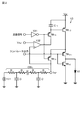
実施例1は、本開示の表示装置に関する。実施例1の表示装置における発光部及び駆動回路から構成された画素等の概念図を図1Aに示し、実施例1の表示装置における駆動回路を構成するコンパレータ回路の回路図を図1Bに示す。また、実施例1の表示装置における駆動回路を構成する電流源の回路図を図2に示し、参考例の電流源の回路図を図3に示す。更に、実施例1の表示装置を構成する回路の概念図を図4に示す。尚、図面の簡素化のため、図4には3×5個の画素を図示している。
Example 1 relates to a display device of the present disclosure. FIG. 1A shows a conceptual diagram of a pixel and the like configured from a light emitting unit and a drive circuit in the display device of Example 1, and FIG. 1B shows a circuit diagram of a comparator circuit that constitutes the drive circuit in the display device of Example 1. Further, FIG. 2 shows a circuit diagram of a current source constituting a driving circuit in the display device of Example 1, and FIG. 3 shows a circuit diagram of a current source of a reference example. Further, FIG. 4 shows a conceptual diagram of a circuit constituting the display device of the first embodiment. For simplification of the drawing, FIG. 4
実施例1の表示装置は、発光部10、及び、発光部10を駆動する駆動回路11から構成された画素(より具体的には、副画素であり、以下においても同様である)1が、複数、2次元マトリクス状に配列されて成る。具体的には、複数の画素1は、第1の方向及び第2の方向に2次元マトリクス状に配列されている。そして、画素群は第1の方向に沿ってP個の画素ブロックに分割されている。各駆動回路11は、
(a)制御パルス線PSL及びデータ線DTLに接続され、制御パルス線PSLからの鋸波形の電圧変化を有する制御パルスLCPとデータ線DTLからの信号電圧(発光強度信号)VSigに基づく電位とを比較し、比較結果に基づく所定電圧(便宜上、『第1の所定電圧』と呼ぶ)を出力するコンパレータ回路12、
(b)発光部10に駆動電流、例えば定電流を供給する電流源13、及び、
(c)コンパレータ回路12からの第1の所定電圧の出力によって作動され、以て、電流源13から発光部10に電流を供給し、発光部10を駆動する発光部駆動用トランジスタTRDrv、
を備えている。尚、信号電圧VSigは、具体的には、画素における発光状態(輝度)を制御する映像信号電圧である。
In the display device of Example 1, a pixel (more specifically, a sub-pixel, which is the same in the following) 1 including a light-emitting
(A) A potential based on a control pulse LCP having a sawtooth voltage change from the control pulse line PSL and a signal voltage (light emission intensity signal) V Sig connected to the control pulse line PSL and the data line DTL.
(B) a
(C) a light emitting unit driving transistor TR Drv that is activated by the output of the first predetermined voltage from the
It has. The signal voltage V Sig is specifically a video signal voltage for controlling the light emission state (luminance) in the pixel.
図1Bに示すように、実施例1のコンパレータ回路12は、例えば、差動型コンパレータ回路から成る。具体的には、コンパレータ回路12は、
信号電圧(発光強度信号)VSigが入力される信号書込みトランジスタTRSig、
信号書込みトランジスタTRSigに接続され、信号書込みトランジスタTRSigの作動に基づき、信号電圧VSigに基づく電位を保持する容量部C0、及び、
容量部C0が保持した信号電圧VSigに基づく電位と制御パルスLCPとを2入力とする差動回路121、
から成る比較部を備えている。
As illustrated in FIG. 1B, the
A signal writing transistor TR Sig to which a signal voltage (light emission intensity signal) V Sig is input;
Is connected to the signal writing transistor TR Sig, based on the operation of the signal writing transistor TR Sig, capacitance section C 0 for holding a potential based on the signal voltage V Sig and,
A
The comparison part which consists of is provided.
尚、ここでは、実施例1のコンパレータ回路12として差動型コンパレータ回路を例示したが、これに限られるものではない。実施例1のコンパレータ回路12としては、差動型コンパレータ回路の他、チョッパー型コンパレータ回路など、種々のタイプのコンパレータ回路を用いることができる。
Although a differential comparator circuit is illustrated here as the
信号書込みトランジスタTRSig及び発光部駆動用トランジスタTRDrvは、ゲート電極、チャネル形成領域及びソース/ドレイン電極から構成された、従来の電界効果トランジスタから成る。信号書込みトランジスタTRSigはnチャネル型の電界効果トランジスタであり、発光部駆動用トランジスタTRDrvはpチャネル型の電界効果トランジスタであるが、このようなチャネル型に限定するものではない。 The signal writing transistor TR Sig and the light emitting unit driving transistor TR Drv are formed of a conventional field effect transistor including a gate electrode, a channel formation region, and a source / drain electrode. The signal writing transistor TR Sig is an n-channel field effect transistor, and the light emitting unit driving transistor TR Drv is a p-channel field effect transistor, but is not limited to such a channel type.
信号書込みトランジスタTRSigのゲート電極は、走査線SCLを介して、表示装置に備えられた走査回路102に接続されている。また、信号書込みトランジスタTRSigの一方のソース/ドレイン電極は、データ線DTLを介して、表示装置に備えられた画像信号出力回路104に接続されている。更には、信号書込みトランジスタTRSigの他方のソース/ドレイン電極は、容量部C0の一端に接続されている。容量部C0の他端は、負電位側の電源(実施例1では、グランドGND)に接続されている。
The gate electrode of the signal writing transistor TR Sig is connected to the
そして、信号書込みトランジスタTRSigには、画像信号出力回路104からデータ線DTLを通して、信号電圧(発光強度信号)VSigが入力される。容量部C0は、信号書込みトランジスタTRSigの作動に基づき、信号電圧VSigに基づく電位を保持する。この信号電圧VSigに基づく電位は、差動回路121の反転(−)入力端に入力される。一方、差動回路121の非反転(+)入力端には、鋸波形の電圧変化を有する制御パルスLCPが入力される。
A signal voltage (light emission intensity signal) V Sig is input to the signal writing transistor TR Sig from the image
発光部駆動用トランジスタTRDrvのゲート電極は、コンパレータ回路12の出力部(出力端)となる、差動回路121の出力部に接続されている。また、発光部駆動用トランジスタTRDrvは、一方のソース/ドレイン電極が、電流源13を介して正電位側の電源Vddに接続され、他方のソース/ドレイン電極が、発光部10に接続されている。発光部10は発光ダイオードから成る。
The gate electrode of the light emitting unit driving transistor TR Drv is connected to the output unit of the
電流源13には、電流供給線CSLを通して、基準定電流供給部101から定電流が供給される。尚、基準定電流供給部101、走査回路102、制御パルス生成回路103、画像信号出力回路104等は、表示装置に配設されていてもよいし、外部に配設されていてもよい。
A constant current is supplied from the reference constant
次に、実施例1の電流源13について説明する。図2に示すように、実施例1の電流源13は、インバータ回路131、差動増幅器132、3つのpチャネル型の電界効果トランジスタTR11,TR12,TR13、及び、1つの容量部C11から成る構成となっている。
Next, the
インバータ回路131には、走査線SCLを介して、表示装置に備えられた走査回路102から走査信号が入力される。差動増幅器132は、基準定電流供給部101から電流供給線CSLを通して供給される所望の定電流に基づく電圧を非反転(+)とし、基準電圧VRefを反転(−)入力端とする。
A scanning signal is input to the
ここで、基準電圧VRefについては、電界効果トランジスタTR13が飽和領域に達する最少のドレイン‐ソース間電圧を、電源電位Vddから差し引いた電位よりも低くし、基準定電流供給部101の接地側でない方の端子が所望の電流を流せる電位に、電流供給線CSLの抵抗に基準定電流供給部101の電流で発生した両端電圧値を加えた電位よりも大きければ、特に厳密に定めなくてよい。その理由は、次のとおりである。
Here, with respect to the reference voltage V Ref , the minimum drain-source voltage at which the field effect transistor TR 13 reaches the saturation region is made lower than the potential subtracted from the power supply potential V dd , and the reference constant
差動増幅器132は理想増幅器であるとし、オフセット電圧は無視できるとする。走査信号がアクティブな区間で電界効果トランジスタTR12のドレイン電圧が基準電圧VRefよりも高ければ、差動増幅器132の出力電圧が上昇する。また、電界効果トランジスタTR11を介して電界効果トランジスタTR13のゲート電圧を上昇させ、当該トランジスタTR13のソース‐ドレイン電流を減少させる。これにより、電界効果トランジスタTR12のドレイン電圧は下降する。
It is assumed that the
また、電界効果トランジスタTR12のドレイン電圧が基準電圧VRefよりも低ければ、差動増幅器132の出力電圧が下降して、電界効果トランジスタTR11を介して電界効果トランジスタTR13のゲート電圧を下降させ、当該トランジスタTR13のソース‐ドレイン電流を増加させる。これにより、電界効果トランジスタTR12のドレイン電圧は上昇する。
If the drain voltage of the field effect transistor TR 12 is lower than the reference voltage V Ref , the output voltage of the
このようにして、電界効果トランジスタTR12のドレイン電圧は、基準電圧VRefに収束し、電界効果トランジスタTR12のドレインの電圧は変化しなくなる。これは、電界効果トランジスタTR13のソースドレイン電流と電流源101の電流が同じ値になったことを意味する。
In this way, the drain voltage of the field effect transistor TR 12 is converged to the reference voltage V Ref, the drain voltage of the field-effect transistor TR 12 is not changed. This means that the source / drain current of the field effect transistor TR 13 and the current of the
つまり、差動増幅器132によって、電界効果トランジスタTR13のゲート電圧は、当該トランジスタTR13のドレイン‐ソース電流が基準定電流供給部101の電流値と同じになる条件下で、電界効果トランジスタTR13のドレイン‐ソース間電圧が電源電位Vddから基準電圧VRefを差し引いたものになるように調整されることを意味する。そして、差動増幅器132の基準電圧VRefの設定電圧は、上記説明した電圧範囲で使えば所望の動作をすることが出来る。以上が、基準電圧VRefについて特に厳密に定めなくてよい理由である。
In other words, the
電界効果トランジスタTR11,TR12は、各ゲート電極がインバータ回路131の出力端に共通に接続されている。従って、電界効果トランジスタTR11,TR12には、走査信号(走査線SCLの電位)がインバータ回路131で極性反転されて入力される。これにより、電界効果トランジスタTR11,TR12は、走査信号に同期してオン/オフ動作を行う。
The gate electrodes of the field effect transistors TR 11 and TR 12 are commonly connected to the output terminal of the
電界効果トランジスタTR11は、一方のソース/ドレイン電極が電界効果トランジスタTR13のゲート電極に接続され、他方のソース/ドレイン電極が差動増幅器132の出力端に接続されている。また、電界効果トランジスタTR12は、一方のソース/ドレイン電極が発光部駆動用トランジスタTRDrvの一方のソース/ドレイン電極に接続され、他方のソース/ドレイン電極が電流供給線CSLに接続されている。
In the field effect transistor TR 11 , one source / drain electrode is connected to the gate electrode of the field effect transistor TR 13 , and the other source / drain electrode is connected to the output terminal of the
電界効果トランジスタTR13は、電流源トランジスタであり(以下、「電流源トランジスタTR13」と記述する場合もある)、ゲート電極が電界効果トランジスタTR11の一方のソース/ドレイン電極に接続されている。電流源トランジスタTR13は更に、一方のソース/ドレイン電極が正電位側の電源Vddに接続され、他方のソース/ドレイン電極が発光部駆動用トランジスタTRDrvの一方のソース/ドレイン電極に接続されている。容量部C11は、一方の電極が正電位側の電源Vddに接続され、他方の電極が電界効果トランジスタTR11の一方のソース/ドレイン電極及び電流源トランジスタTR13のゲート電極に接続されている。 The field effect transistor TR 13 is a current source transistor (hereinafter also referred to as “current source transistor TR 13 ”), and has a gate electrode connected to one source / drain electrode of the field effect transistor TR 11 . . In the current source transistor TR 13 , one source / drain electrode is further connected to the power source V dd on the positive potential side, and the other source / drain electrode is connected to one source / drain electrode of the light emitting unit driving transistor TR Drv. ing. The capacitor C 11 has one electrode connected to the positive potential side power supply V dd , and the other electrode connected to one source / drain electrode of the field effect transistor TR 11 and the gate electrode of the current source transistor TR 13. Yes.
以上に説明した構成の実施例1の電流源13は、電流書き込み型の定電流回路である。そして、差動増幅器132の出力は、走査信号に同期してオン/オフ動作を行う電界効果トランジスタTR11を介して電流源トランジスタTR13のゲート電極に与えられる。尚、実施例1の電流源13を用いる駆動回路にあっては、発光部10に対してnチャネル型の電界効果トランジスタTR00が並列に接続された構成となっている。
The
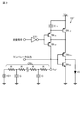
ところで、画素1の駆動回路11を構成する電流源13は、各色毎に同一の電流値でばらつきが少ないことが必要とされる。電流値のばらつきを少なくできる回路としては、図3に示す、電流書き込み型の定電流回路が考えられる。この電流書き込み型の定電流回路について、参考例の電流源13’として以下に説明する。
By the way, the
図3に示すように、参考例の電流源13’は、インバータ回路131、3つのpチャネル型の電界効果トランジスタTR11,TR12,TR13、及び、1つの容量部C11から成る構成となっている。
As shown in FIG. 3, the
インバータ回路131には、走査線SCLを介して、表示装置に備えられた走査回路102から走査信号が入力される。電界効果トランジスタTR11,TR12は、互いに直列に接続され、各ゲート電極がインバータ回路131の出力端に共通に接続されている。従って、電界効果トランジスタTR11,TR12には、走査信号(走査線SCLの電位)がインバータ回路131で極性反転されて入力される。
A scanning signal is input to the
電流源トランジスタTR13は、ゲート電極が電界効果トランジスタTR11の一方のソース/ドレイン電極に接続されている。電流源トランジスタTR13は更に、一方のソース/ドレイン電極が正電位側の電源Vddに接続され、他方のソース/ドレイン電極が発光部駆動用トランジスタTRDrvの一方のソース/ドレイン電極に接続されている。容量部C11は、一方の電極が正電位側の電源Vddに接続され、他方の電極が電界効果トランジスタTR11の一方のソース/ドレイン電極及び電流源トランジスタTR13のゲート電極に接続されている。 The current source transistor TR 13 has a gate electrode connected to one source / drain electrode of the field effect transistor TR 11 . In the current source transistor TR 13 , one source / drain electrode is further connected to the power source V dd on the positive potential side, and the other source / drain electrode is connected to one source / drain electrode of the light emitting unit driving transistor TR Drv. ing. The capacitor C 11 has one electrode connected to the positive potential side power supply V dd , and the other electrode connected to one source / drain electrode of the field effect transistor TR 11 and the gate electrode of the current source transistor TR 13. Yes.
電界効果トランジスタTR11,TR12の共通接続ノード、即ち、電界効果トランジスタTR11の他方のソース/ドレイン電極及び電界効果トランジスタTR12の一方のソース/ドレイン電極は、電流源トランジスタTR13の他方のソース/ドレイン電極に接続されている。 The common connection node of the field effect transistors TR 11 and TR 12 , that is, the other source / drain electrode of the field effect transistor TR 11 and one source / drain electrode of the field effect transistor TR 12 are the other of the current source transistors TR 13 . Connected to source / drain electrodes.
以上に説明した構成の電流書き込み型の定電流回路から成る電流源13’は、参考例である。この参考例の電流源13’の入力端、より具体的には、電界効果トランジスタTR12の他方のソース/ドレイン電極には、電流供給線CSLを通して、基準定電流供給部101から所望の定電流IRefが供給される。
The
この参考例の電流源13’の回路動作は次のとおりである。即ち、走査信号(走査線SCLの電位)が高レベルになると、電界効果トランジスタTR11,TR12が共にオン状態になる。すると、これら電界効果トランジスタTR11,TR12を介して、電流源トランジスタTR13に基準定電流供給部101の基準定電流IRefが流れる。そのときに、容量部C11の両端電圧は、電流源トランジスタTR13に基準定電流供給部101と同じ電流を流す電圧となる。
The circuit operation of the current source 13 'of this reference example is as follows. That is, when the scanning signal (the potential of the scanning line SCL) becomes high level, both the field effect transistors TR 11 and TR 12 are turned on. Then, the reference constant current I Ref of the reference constant
走査信号が低レベルの区間では、電界効果トランジスタTR11がオフ状態になることによって容量部C11が切り離され、当該容量部C11は電流源トランジスタTR13に基準定電流供給部101と同じ電流を流す電圧を保持する。そして、コンパレータ回路12の出力が第1の所定電圧(L)になると、電流源トランジスタTR13は、容量部C11の保持電圧に基づいて、基準定電流供給部101と同じ電流を発光部10に流す。
In scan signal is low level section, the capacitance section C 11 is disconnected by the field-effect transistor TR 11 is turned off, the capacitor portion C 11 is the same current as the reference constant
上述したように、参考例の電流源13’は、電流源トランジスタTR13に基準定電流供給部101と同じ電流を流す電圧を容量部C11に保持し、この保持した電圧に基づいて、基準定電流供給部101と同じ電流を発光部10に流すように動作する。従って、電流源トランジスタTR13の画素毎の特性ばらつきを考慮する必要がなくなる利点がある。この点については、実施例1の電流源13にあっても基本的に同じである。
As described above, the current source 13 'of the reference example, and stores the voltage the same current as the reference constant
ところで、電流書き込み型の電流源を用いて表示装置を構成するには、基準定電流供給部(基準定電流源)101を、1垂直ライン(1画素列)に各色1つ配置し、垂直ラインの全ての画素が当該基準定電流源101に繋がるようにするのが最も効率がよい。この場合、画素の位置によっては、基準定電流供給部101はかなり長距離の配線(電流供給線CSL)を経て画素回路に接続されることになる。即ち、各画素の電流源13には基準定電流供給部101から、垂直ライン(画素列)毎に配線された電流供給線CSLを通して基準定電流IRefが供給される。従って、実際には、図3に示すように、容量部C11には電流供給線CSLの配線抵抗Rや配線容量Cも接続されていることになる。通常、容量部C11の容量値よりも配線容量Cの容量値の方が大きい。
By the way, in order to configure a display device using a current writing type current source, a reference constant current supply unit (reference constant current source) 101 is arranged for each color in one vertical line (one pixel column), and a vertical line is formed. It is most efficient to connect all of the pixels to the reference constant
一方、走査信号は、水平ライン(画素行)間の混線を避けるために、隣接する水平ラインが非アクティブ状態になってから、少しのラグ時間を経てアクティブ状態になる。そのラグ時間の間に、基準定電流供給部101による電流流出のために配線(電流供給線CSL)の電位が少し低下する。この少し低下した配線の電位を、電流源トランジスタTR13が基準定電流供給部101の基準定電流IRefと同じ電流を流す電位になるまで、走査信号のアクティブ区間内に上げなければならない。
On the other hand, in order to avoid cross-talk between horizontal lines (pixel rows), the scanning signal becomes active after a short lag time after the adjacent horizontal line becomes inactive. During the lag time, the potential of the wiring (current supply line CSL) slightly decreases due to current outflow by the reference constant
しかしながら、電流供給線CSLの配線容量Cと容量部C11とを充電し、配線の電位を変える電流値はこの両者の差分の電流値だけで、電流源トランジスタTR13の電流が基準定電流供給部101の基準定電流IRefに近づくにつれて小さくなってしまう。結果として、容量部C11の電圧が所望の電圧に達するのに要する時間が長くなり(所謂セトリング問題)、走査信号のアクティブ区間内に容量部C11の電圧が所望の電圧に達することができないこともあり得る。そして、容量部C11の電圧が所望の電圧に達しないと、定電流書き込みが事実上できなくなるため、電流源トランジスタTR13の電流値がばらついてしまう。
However, the current value for charging the wiring capacitance C and the capacitance portion C 11 of the current supply line CSL and changing the potential of the wiring is only the current value of the difference between the two, and the current of the current source transistor TR 13 is the reference constant current supply. It becomes smaller as it approaches the reference constant current I Ref of the
これに対して、実施例1の電流源13にあっては、走査信号のアクティブ区間内に、差動増幅器132が電流源トランジスタTR13のゲート電位をコントロールする。具体的には、走査信号のアクティブ区間では、電界効果トランジスタTR11がオン状態にある。そして、走査信号のアクティブ区間において、配線(電流供給線CSL)の電位が基準電圧VRefよりも低い場合は、差動増幅器132は、電流源トランジスタTR13のゲート電位を下げることによって、電界効果トランジスタTR12が、電流源トランジスタTR13に流れる電流に応じて配線(電流供給線CSL)の電位を上げる方向に素早くコントロールする。これにより、容量部C11の電圧が所望の電圧に達する(収束する)のに要する時間を早くすることができる。即ち、電流源トランジスタTR13のゲート電位の収束に時間がかかるセトリング問題を解消できる。そして、電流源トランジスタTR13の電流を、基準定電流供給部101の基準定電流IRefに合わせることができる。
On the other hand, in the
図5に、実施例1の電流源の具体的な回路構成の一例を示す。差動増幅器132は、例えば、電界効果トランジスタによって次のように構成されている。pチャネル型の電界効果トランジスタTR21,TR22は、差動対トランジスタであり(以下、「差動対トランジスタTR21,TR22」と記述する場合もある)、ソース電極が共通に接続されて差動回路を構成している。そして、一方の差動対トランジスタTR21は、基準電圧VRefをゲート入力とし、他方の差動対トランジスタTR22は、配線(電流供給線CSL)の電位をゲート入力としている。
FIG. 5 shows an example of a specific circuit configuration of the current source according to the first embodiment. The
nチャネル型の電界効果トランジスタTR23,TR24は、上記の差動回路の能動負荷となるカレントミラー回路を構成している。電界効果トランジスタTR23は、ドレイン電極及びゲート電極が共に一方の差動対トランジスタTR21のドレイン電極に接続され、ソース電極が低電位側の電源GNDに接続されている。電界効果トランジスタTR24は、ゲート電極が電界効果トランジスタTR23のゲート電極に接続され、ドレイン電極が他方の差動対トランジスタTR22のドレイン電極に接続され、ソース電極が低電位側の電源GNDに接続されている。 The n-channel type field effect transistors TR 23 and TR 24 constitute a current mirror circuit serving as an active load of the differential circuit. Field effect transistor TR 23 has a drain electrode and a gate electrode connected to the drain electrode of both the one of the differential pair transistors TR 21, the source electrode is connected to the power supply GND on the low potential side. In the field effect transistor TR 24 , the gate electrode is connected to the gate electrode of the field effect transistor TR 23 , the drain electrode is connected to the drain electrode of the other differential transistor TR 22 , and the source electrode is connected to the power supply GND on the low potential side. It is connected.
pチャネル型の電界効果トランジスタTR25は、上記の差動回路に定電流を供給する定電流源トランジスタであり(以下、「定電流源トランジスタTR25」と記述する場合もある)、差動対トランジスタTR21,TR22のソース共通接続ノードと正電位側の電源Vddとの間に接続されている。定電流源トランジスタTR25のゲート電極には、pチャネル型の電界効果トランジスタTR26,TR27,TR28及びnチャネル型の電界効果トランジスタTR29,TR30から成る定電圧回路で生成される一定の電圧が印加される。 The p-channel field effect transistor TR 25 is a constant current source transistor that supplies a constant current to the above-described differential circuit (hereinafter may be referred to as “constant current source transistor TR 25 ”), and is a differential pair. The transistors TR 21 and TR 22 are connected between the common source connection node and the power source V dd on the positive potential side. The constant current source transistor TR 25 has a gate electrode formed with a constant voltage generated by a constant voltage circuit including p-channel field effect transistors TR 26 , TR 27 , TR 28 and n-channel field effect transistors TR 29 , TR 30. Is applied.
上記の定電圧回路において、pチャネル型の電界効果トランジスタTR26,TR27,TR28及びnチャネル型の電界効果トランジスタTR29,TR30が、正電位側の電源Vddと低電位側の電源GNDとの間に直列に接続されている。電界効果トランジスタTR26は、ゲート電極が定電流源トランジスタTR25のゲート電極に接続されている。電界効果トランジスタTR27は、インバータ回路131で反転された反転走査信号をゲート入力とすることで、走査信号のアクティブ区間にオン状態になり、定電圧回路を作動状態とする。電界効果トランジスタTR 26 ,TR 28 ,TR29,TR30は、ゲート電極とドレイン電極とが共通に接続されたダイオード接続構成となっている。
In the above constant voltage circuit, the p-channel field effect transistors TR 26 , TR 27 , TR 28 and the n-channel field effect transistors TR 29 , TR 30 are connected to the positive potential side power source V dd and the low potential side power source. It is connected in series with GND. Field effect transistor TR 26 has a gate electrode connected to the gate electrode of the constant current source transistor TR 25. Field effect transistor TR 27 is, by the inverted scanning signal inverted by the
上記の差動回路において、他方の差動対トランジスタTR22と電界効果トランジスタTR24とのドレイン共通接続ノードが、当該差動回路の出力ノードとなっている。そして、この出力ノードと低電位側の電源GNDとの間にnチャネル型の電界効果トランジスタTR31が接続されている。この電界効果トランジスタTR31は、インバータ回路131で反転された反転走査信号をゲート入力とし、走査信号の非アクティブ区間でオン状態、アクティブ区間でオフ状態になる。差動回路の出力ノードには、ソース接地回路を構成するnチャネル型の電界効果トランジスタTR32のゲート電極が接続されている。そして、電界効果トランジスタTR32のドレイン電極が本差動増幅器132の出力ノードとなる。この出力ノードと正電位側の電源Vddとの間には、ダイオード接続構成のpチャネル型の電界効果トランジスタTR33が接続されている。
In the above differential circuit, the drain common connection node of the other differential pair transistor TR 22 and the field effect transistor TR 24 is an output node of the differential circuit. An n-channel field effect transistor TR 31 is connected between the output node and the power supply GND on the low potential side. The field effect transistor TR 31 receives the inverted scanning signal inverted by the
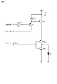
実施例2は、実施例1の変形である。実施例2の表示装置における駆動回路を構成する電流源の回路図を図6に示し、また、実施例2の表示装置を構成する回路の概念図を図7に示す。 The second embodiment is a modification of the first embodiment. FIG. 6 shows a circuit diagram of a current source constituting a drive circuit in the display device of the second embodiment, and FIG. 7 shows a conceptual diagram of a circuit constituting the display device of the second embodiment.
先述した電流書き込み型の定電流回路にあっては、電流源トランジスタTR13のゲート電極に対する書き込み電圧の収束問題(セトリング問題)があり、あまり早い書き込み時間に対応するのが難しい。また、実施例1の電流源13にあっては、差動増幅器132を構成する素子数が多いため、回路面積的に不利な面がある。
In the constant current circuit of the foregoing the current writing type, there is a convergence problems of the write voltage to the gate electrode of the current source transistor TR 13 (settling issues), it is difficult to correspond to the much faster writing time. In addition, the
これに対して、実施例2にあっては、電流源トランジスタTR13のゲート電極に対して画素個々に設定された電圧を直接書き込む(与える)構成を採る。そして、この構成を採ることによって、電流源トランジスタTR13のゲート電極に対する書き込み電圧の収束問題(セトリング問題)を解消できる。具体的には、実施例2にあっては、駆動回路11を構成する電流源13として、図6に回路図を示す電圧書き込み型の定電流回路を用いる。
In contrast, in Example 2, and writes the voltage set to the pixel individually for the gate electrode of the current source transistor TR 13 directly (giving) a configuration. Then, by adopting this configuration, it eliminates the convergence problems of the write voltage to the gate electrode of the current source transistor TR 13 (settling issues). Specifically, in the second embodiment, a voltage writing type constant current circuit whose circuit diagram is shown in FIG. 6 is used as the
ところで、電圧書き込み型の定電流回路にあっては、各画素の電流源トランジスタTR13に対して同じ電圧を書き込んだとしても、電流源トランジスタTR13の画素毎の特性ばらつきにより、電流源トランジスタTR13に流れる電流値がばらつく場合がある。そこで、実施例2の表示装置にあっては、図7に示すように、電圧書き込み回路105を有し、当該電圧書き込み回路105から、画素列毎に配線された電圧供給線VSLを通して、電流源トランジスタTR13のゲート電極に対して画素各々に別々の電圧値を直接書き込むようにする。
By the way, in the voltage writing type constant current circuit, even if the same voltage is written to the current source transistor TR 13 of each pixel, the current source transistor TR 13 varies due to the characteristic variation of each pixel of the current source transistor TR 13 . The current value flowing through 13 may vary. Therefore, in the display device according to the second embodiment, as illustrated in FIG. 7, the
通常、各画素1の発光部10となる発光ダイオードの特性は画素毎にばらついている。この発光ダイオードの特性ばらつきは、画面の表示ムラとなって視認される。そこで、あらかじめ、各画素毎に、発光ダイオードの特性ばらつきや、電流源トランジスタTR13の特性ばらつきを考慮して、これらのばらつきを補正する電圧値を設定し、電圧書き込み回路105に格納しておく。そして、電流源トランジスタTR13や発光ダイオードの画素毎の特性ばらつきを考慮して画素毎に別々に設定した電圧値を、電圧書き込み回路105から電圧供給線VSLを通して、電流源トランジスタTR13のゲート電極に対して画素行単位で直接書き込む。
Usually, the characteristics of the light-emitting diodes that become the light-emitting
このように、電流源トランジスタTR13や発光ダイオードの特性ばらつきを考慮して、画素各々に別々の電圧値を書き込むシステム構成を採ることで、電流源トランジスタTR13の画素毎の特性ばらつきを補正できるとともに、発光ダイオードの画素毎の特性ばらつきについても補正することができる。つまり、画素毎に別々に設定した電圧値を各画素に書き込むことで、電流源トランジスタTR13に流れる電流値を画素毎に微調整することができるため、特に、発光ダイオードの特性ばらつきに起因する画面の表示ムラを補正可能な表示装置を実現することができる。 In this way, by taking into account the characteristic variation of the current source transistor TR 13 and the light emitting diode, by adopting a system configuration in which different voltage values are written to each pixel, the characteristic variation for each pixel of the current source transistor TR 13 can be corrected. At the same time, it is possible to correct variations in characteristics of each pixel of the light emitting diode. That is, by writing a voltage value set separately for each pixel to each pixel, the current value flowing through the current source transistor TR 13 can be finely adjusted for each pixel. A display device capable of correcting display unevenness on the screen can be realized.
実施例3は、実施例1あるいは実施例2の変形である。図8に、実施例3の表示装置において、1つの画素の動作を説明するための制御パルス等を示す模式図を示す。また、実施例3の表示装置における画素ブロックへの複数の制御パルスの供給を模式的に図9に示す。更には、本開示の表示装置における制御パルス生成回路の概念図を図11に示す。尚、図9及び後述する図10においては、制御パルスの鋸波形を、便宜上、三角形で示している。 The third embodiment is a modification of the first or second embodiment. FIG. 8 is a schematic diagram illustrating control pulses and the like for explaining the operation of one pixel in the display device according to the third embodiment. FIG. 9 schematically shows the supply of a plurality of control pulses to the pixel block in the display device according to the third embodiment. Furthermore, FIG. 11 shows a conceptual diagram of a control pulse generation circuit in the display device of the present disclosure. In FIG. 9 and FIG. 10 described later, the sawtooth waveform of the control pulse is indicated by a triangle for convenience.
実施例3の表示装置は、発光部10、及び、発光部10を駆動する駆動回路11から構成された画素1が、複数、第1の方向及び第2の方向に2次元マトリクス状に配列され、画素群は第1の方向に沿ってP個の画素ブロックに分割されて成る表示装置である。そして、第1番目の画素ブロックに属する画素1を構成する発光部10から、第P番目の画素ブロックに属する画素1を構成する発光部10まで、画素ブロック毎に、順次、一斉に発光させ、且つ、一部の画素ブロックに属する画素1を構成する発光部10を発光させているとき、残りの画素ブロックに属する画素1を構成する発光部10を発光させない。
In the display device according to the third embodiment, a plurality of
例えば、画面の水平方向(第2の方向)の画素数が1920、画面の垂直方向(第1の方向)の画素数が1080であるフルHD高精細フルカラー表示装置を想定する。画素群は、第1の方向に沿ってP個の画素ブロックに分割されているが、P=6とする。すると、第1番目の画素ブロックには第1行目の画素群から第180行目の画素群が含まれ、第2番目の画素ブロックには第181行目の画素群から第360行目の画素群が含まれ、第3番目の画素ブロックには第361行目の画素群から第540行目の画素群が含まれ、第4番目の画素ブロックには第541行目の画素群から第720行目の画素群が含まれ、第5番目の画素ブロックには第721行目の画素群から第900行目の画素群が含まれ、第6番目の画素ブロックには第901行目の画素群から第1080行目の画素群が含まれる。 For example, a full HD high-definition full-color display device in which the number of pixels in the horizontal direction (second direction) of the screen is 1920 and the number of pixels in the vertical direction (first direction) of the screen is 1080 is assumed. The pixel group is divided into P pixel blocks along the first direction, and P = 6. Then, the first pixel block includes the pixel group from the pixel group of the first row to the 180th row, and the second pixel block includes the pixel group of the 181st row to the 360th row. The pixel group is included, the third pixel block includes the pixel group of the 361st row to the 540th row, and the fourth pixel block includes the pixel group of the 541st row. The pixel group of the 720th row is included, the pixel group of the 900th row from the pixel group of the 721st row is included in the fifth pixel block, and the 901th row is included in the sixth pixel block. The pixel group in the 1080th row from the pixel group is included.
以下、第1番目の画素ブロックにおける各画素の動作を説明する。 Hereinafter, the operation of each pixel in the first pixel block will be described.
[信号電圧書込み期間]
実施例1において説明したように、容量部C0には、データ線DTLの電位、即ち、信号電圧VSigに基づく電位に応じた電荷が蓄積される。云い換えれば、容量部C0は、信号電圧に基づく電位を保持する。ここで、第1番目の画素ブロックにおいて、第2の方向に配列された1列に属する全ての画素(行方向画素群)における駆動回路11(具体的には、信号書込みトランジスタTRSig)を、一斉に作動状態とする。そして、第1番目の画素ブロックにおいて、第2の方向に配列された1列に属する全ての画素(行方向画素群)における駆動回路11(具体的には、信号書込みトランジスタTRSig)が一斉に作動状態となる動作が、第1の方向に配列された第1行目に属する全ての画素(第1行目の行方向画素群)における駆動回路11(具体的には、信号書込みトランジスタTRSig)から最終行(具体的には、第180行目)に属する全ての画素(最終行の行方向画素群)における駆動回路11(具体的には、信号書込みトランジスタTRSig)まで、順次、行われる。
[Signal voltage writing period]
As described in the first embodiment, charges corresponding to the potential of the data line DTL, that is, the potential based on the signal voltage V Sig are accumulated in the capacitor C 0 . In other words, the capacitor C 0 holds a potential based on the signal voltage. Here, in the first pixel block, the drive circuit 11 (specifically, the signal write transistor TR Sig ) in all the pixels (row direction pixel group) belonging to one column arranged in the second direction, Activate all at once. In the first pixel block, the drive circuits 11 (specifically, the signal write transistors TR Sig ) in all the pixels (row direction pixel group) belonging to one column arranged in the second direction are simultaneously formed. The operation to be activated is the drive circuit 11 (specifically, the signal write transistor TR Sig in all the pixels belonging to the first row arranged in the first direction (row direction pixel group of the first row)). ) To the drive circuit 11 (specifically, the signal write transistor TR Sig ) in all pixels (specifically, the row direction pixel group of the final row) belonging to the final row (specifically, the 180th row) Is called.
[画素ブロック発光期間]
第1番目の画素ブロックにおいて、以上の動作が完了すると、制御パルス生成回路103から、第1番目の画素ブロックに制御パルスLCPが供給される。即ち、第1番目の画素ブロックにおける全画素1を構成する駆動回路11(具体的には、発光部駆動用トランジスタTRDrv)が一斉に作動状態となり、第1番目の画素ブロックに属する全画素1における発光部10が発光する。1つの制御パルスLCPの電圧の絶対値は、時間の経過と共に、増加し、次いで、減少する。尚、図8に示す例では、1つの制御パルスLCPの電圧は、時間の経過と共に、減少し、次いで、増加する。そして、時間の経過と共に変化する制御パルスLCPの電圧によってガンマ補正がなされる。即ち、時間を変数とした制御パルスLCPの電圧の変化率(微分値)の絶対値は、定数2.2に比例する。
[Pixel block emission period]
When the above operation is completed in the first pixel block, the control pulse LCP is supplied from the control
図8に示した例において、信号電圧書込み期間にあっては、制御パルスLCPの電圧は、例えば、3ボルト以上である。従って、信号電圧書込み期間にあっては、コンパレータ回路12は、出力部から第2の所定電圧(H)を出力するので、発光部駆動用トランジスタTRDrvはオフ状態にある。画素ブロック発光期間において、制御パルスLCPの電圧が下降し始め、制御パルスLCPの鋸波形の電圧が信号電圧VSigに基づく電位以下になると、コンパレータ回路12は、出力部から第1の所定電圧(L)を出力する。その結果、発光部駆動用トランジスタTRDrvはオン状態となり、電流供給線CSLから発光部10に電流が供給され、発光部10が発光する。制御パルスLCPの電圧は約1ボルトまで下降し、次いで、上昇に転じる。そして、制御パルスLCPの鋸波形の電圧と信号電圧VSigに基づく電位を超えると、コンパレータ回路12は、出力部から第2の所定電圧(H)を出力する。その結果、発光部駆動用トランジスタTRDrvはオフ状態となり、電流供給線CSLから発光部10への電流の供給が遮断され、発光部10は発光を中止する。即ち、信号電圧(発光強度信号)VSigに基づく電位が制御パルスLCPの鋸波形を切り取る時間の間のみ、発光部10を発光させることができる。そして、このときの発光部10の輝度は、切り取られる時間の長短に依存する。
In the example shown in FIG. 8, during the signal voltage writing period, the voltage of the control pulse LCP is, for example, 3 volts or more. Accordingly, in the signal voltage writing period, the
即ち、発光部10が発光する時間は、容量部C0に保持された電位と制御パルス生成回路103からの制御パルスLCPの電圧とに基づく。そして、時間の経過と共に変化する制御パルスLCPの鋸波形の電圧によってガンマ補正がなされる。即ち、時間を変数とした制御パルスLCPの電圧の変化率の絶対値は、定数2.2に比例するので、ガンマ補正のための回路を設けることは不要である。例えば、線形の鋸波形の電圧(三角波形)を有する制御パルスを用い、信号電圧VSigを線形の輝度信号に対して2.2乗で変化させる方法も考えられるが、実際には低輝度で電圧変化が小さくなり過ぎ、特に、このような電圧変化をデジタル処理にて実現するためには、大きなビット数が必要とされ、有効な方法とは云えない。
That is, the time during which the
実施例3にあっては、制御パルス生成回路103が1つ備えられている。制御パルスLCPの電圧の変化は、図8に模式的に示すように、低階調部(低電圧部分)が非常に急峻に変化しており、特にこの部分の制御パルス波形の波形品位に対して敏感である。従って、制御パルス生成回路103において生成された制御パルスLCPのばらつきも考慮する必要がある。然るに、実施例3の表示装置にあっては、制御パルス生成回路103を1つしか備えていないので、制御パルス生成回路において生成された制御パルスLCPに、実質的に、ばらつきが生じることがない。即ち、表示装置全体を同一の制御パルス波形によって発光させることができるので、発光状態のばらつき発生を防止することができる。また、制御パルスLCPの電圧の絶対値は、時間の経過と共に、増加し、次いで、減少するので、1つの画素ブロックに属する全画素(より具体的には、全副画素)を構成する発光部を、同じタイミングで発光させることができる。即ち、各画素ブロックに属する全画素を構成する発光部の発光の時間的重心を揃える(一致させる)ことができる。それ故、列方向画素群における発光の遅延に起因した、画像上の縦線(縦筋)発生を確実に防止することができる。
In the third embodiment, one control
実施例3の表示装置にあっては、複数の制御パルスLCPに基づき、発光部10が、複数回、発光する。あるいは又、駆動回路11に供給される鋸波形の電圧変化を有する複数の制御パルスLCPと、信号電圧VSigに基づく電位とに基づき、発光部10が、複数回、発光する。あるいは又、制御パルス生成回路103にあっては、複数の制御パルスLCPに基づき、発光部10を、複数回、発光させる。複数の制御パルスLCPの時間間隔は一定である。具体的には、実施例3にあっては、画素ブロック発光期間において、4つの制御パルスLCPが、各画素ブロックを構成する全画素1に送られ、各画素1は、4回、発光する。
In the display device according to the third embodiment, the
図9に模式的に示すように、実施例3の表示装置にあっては、1表示フレームにおいて、12個の制御パルスLCPが6つの画素ブロックへ供給される。そして、1表示フレーム内における制御パルスLCPの数よりも、1表示フレーム内における駆動回路11に供給される制御パルスLCPの数は少ない。あるいは又、制御パルス生成回路103にあっては、1表示フレーム内における制御パルスLCPの数よりも、1表示フレーム内における駆動回路11に供給される制御パルスLCPの数は少ない。具体的には、図9に示した例では、1表示フレーム内における制御パルスLCPの数は12であり、1表示フレーム内における駆動回路11に供給される制御パルスLCPの数は4である。隣接する画素ブロックにあっては、2つの制御パルスLCPが重なりあっている。即ち、2つ隣接する画素ブロックが同時に発光状態となる。また、第1番目の画素ブロックと最終番目の画素ブロックにあっても同時に発光状態となる。このような形態は、1表示フレームにおいて一連の複数の制御パルスLCPを生成し、一の画素ブロックに属する画素1を構成する発光部10を発光させないとき、一連の複数の制御パルスLCPの一部をマスクして、一の画素ブロックに属する画素1を構成する駆動回路11には制御パルスLCPを供給しないことで達成することができる。具体的には、例えば、マルチプレクサを用いて、1表示フレーム内における一連の制御パルスLCPから一部分(4つの連続した制御パルスLCP)を取り出し、駆動回路11に供給すればよい。
As schematically shown in FIG. 9, in the display device according to the third embodiment, 12 control pulses LCP are supplied to 6 pixel blocks in one display frame. The number of control pulses LCP supplied to the
即ち、実施例3の制御パルス生成回路103は、発光部10、及び、信号電圧VSigに基づく電位に応じた時間だけ発光部10を発光させる駆動回路11から構成された画素1が、複数、第1の方向及び第2の方向に2次元マトリクス状に配列され、画素群は第1の方向に沿ってP個の画素ブロックに分割されて成る表示装置における駆動回路11を制御するための、鋸波形の電圧変化を有する制御パルスLCPを生成する制御パルス生成回路である。そして、制御パルス生成回路103は、第1番目の画素ブロックに属する画素1を構成する駆動回路11から、第P番目の画素ブロックに属する画素1を構成する駆動回路11まで、画素ブロック毎に、順次、一斉に制御パルスLCPを供給し、且つ、一部の画素ブロックに属する画素1を構成する駆動回路11に制御パルスLCPを供給しているとき、残りの画素ブロックに属する画素1を構成する駆動回路11に制御パルスLCPを供給しない。ここで、制御パルス生成回路103にあっては、1表示フレームにおいて一連の複数の制御パルスLCPを生成し、一の画素ブロックに属する画素1を構成する発光部10を発光させないとき、一連の複数の制御パルスLCPの一部をマスクして、一の画素ブロックに属する画素1を構成する駆動回路11には制御パルスLCPを供給しない。
That is, the control
より具体的には、図11に概念図を示すように、制御パルス生成回路103において、メモリ21に格納してある制御パルスの波形信号データをコントローラ22によって読み出し、読み出された波形信号データをD/Aコンバータ23に送り、D/Aコンバータ23において電圧に変換し、電圧をローパスフィルター24で積分することで、2.2乗カーブを有する制御パルスを作成する。そして、制御パルスをアンプリファイア25を介して、複数(実施例3にあっては6個)のマルチプレクサ26に分配し、コントローラ22の制御下、マルチプレクサ26によって、一連の制御パルスLCPにおいて必要とされる一部分だけを通し、その他の部分をマスクすることで、所望の制御パルス群(具体的には、4つの連続した制御パルスLCPから成る制御パルス群を6組)を作成する。尚、元となる鋸波形は1つであるので、制御パルス生成回路103における制御パルスLCPの生成におけるばらつき発生を確実に抑制することができる。
More specifically, as shown in the conceptual diagram of FIG. 11, in the control
そして、以上に説明した信号電圧書込み期間及び画素ブロック発光期間における動作を、第1番目の画素ブロックから第6番目の画素ブロックまで、順次、実行する。即ち、図9に示すように、第1番目の画素ブロックに属する画素1を構成する発光部10から、第P番目の画素ブロックに属する画素1を構成する発光部10まで、画素ブロック毎に、順次、一斉に発光させる。しかも、一部の画素ブロックに属する画素1を構成する発光部10を発光させているとき、残りの画素ブロックに属する画素1を構成する発光部10を発光させない。尚、1表示フレームにおいて、常に、いずれかの画素ブロックが発光している。
Then, the operations in the signal voltage writing period and the pixel block light emission period described above are sequentially executed from the first pixel block to the sixth pixel block. That is, as shown in FIG. 9, for each pixel block from the
ところで、1表示フレーム期間の初めの第1の期間に、全画素の発光を停止させた状態で、全画素に映像信号電圧を書き込み、第2の期間に、各画素に書き込まれた映像信号電圧により決定される少なくとも1回の発光期間内に、全画素の発光部を発光させるといった従来の駆動方法では、以下のような問題が生じる。即ち、映像信号は、1表示フレーム全ての時間に亙り、均等に送られて来る場合が多い。従って、テレビジョン受像システムにおいて、垂直ブランキング区間を第2の期間に充当させれば、全画素を同時に発光させる方法も考えられる。しかしながら、垂直ブランキング区間は、通常、1表示フレームの4%程度の時間長さである。それ故、発光効率が非常に低い表示装置となってしまう。また、1表示フレームに亙り送られてくる映像信号を第1の期間において全ての画素に書き込むためには、大きな信号バッファを用意する必要があるし、転送されてくる映像信号レート以上のスピードで各画素に映像信号を伝送するために、信号伝送回路の工夫が必要になる。更には、第2の期間において全画素を一斉に発光させるので、発光に要する電力が短時間に集中してしまい、電源設計が難しくなるという問題もある。 By the way, in the first period of one display frame period, the video signal voltage is written to all the pixels while the light emission of all the pixels is stopped, and the video signal voltage written to each pixel in the second period. In the conventional driving method in which the light emitting portions of all the pixels emit light within at least one light emission period determined by the following problem occurs. That is, video signals are often sent evenly over the entire time of one display frame. Therefore, in the television image receiving system, if the vertical blanking interval is applied to the second period, a method of simultaneously emitting light from all the pixels can be considered. However, the vertical blanking interval is usually about 4% of the time length of one display frame. Therefore, the display device has a very low luminous efficiency. In order to write a video signal sent over one display frame to all the pixels in the first period, it is necessary to prepare a large signal buffer and at a speed higher than the rate of the transferred video signal. In order to transmit a video signal to each pixel, it is necessary to devise a signal transmission circuit. Furthermore, since all the pixels emit light at the same time in the second period, there is a problem that the power required for light emission is concentrated in a short time, making it difficult to design the power supply.
これに対して、実施例3にあっては、一部の画素ブロック(例えば、第1番目及び第2番目の画素ブロック)に属する画素を構成する発光部を発光させているとき、残りの画素ブロック(例えば、第3番目から第6番目の画素ブロック)に属する画素を構成する発光部を発光させないので、PWM駆動法に基づく表示装置の駆動において、発光期間を長くすることが可能となり、発光効率の向上を図ることができる。しかも、1表示フレームに亙り送られてくる映像信号を或る期間内に全ての画素に一斉に書き込む必要がないので、即ち、従来の表示装置と同様に、1表示フレームに亙り送られてくる映像信号を、行方向画素群毎に、順次、書き込めばよいので、大きな信号バッファを用意する必要がないし、転送されてくる映像信号レート以上のスピードで各画素に映像信号を伝送するための信号伝送回路の工夫も不要である。更には、画素の発光期間において、全画素を一斉に発光させるのではないので、即ち、例えば、第1番目及び第2番目の画素ブロックに属する画素を構成する発光部を発光させているとき、第3番目から第6番目の画素ブロックに属する画素を構成する発光部を発光させないので、発光に要する電力が短時間に集中することがなくなり、電源設計が容易となる。 On the other hand, in Example 3, when the light emitting units constituting the pixels belonging to some of the pixel blocks (for example, the first and second pixel blocks) are caused to emit light, the remaining pixels Since the light emitting units constituting the pixels belonging to the block (for example, the third to sixth pixel blocks) are not caused to emit light, it is possible to lengthen the light emission period in driving the display device based on the PWM driving method. Efficiency can be improved. In addition, since it is not necessary to simultaneously write the video signals sent over one display frame to all the pixels within a certain period, that is, like the conventional display device, they are sent over one display frame. Since it is only necessary to sequentially write the video signal for each pixel group in the row direction, it is not necessary to prepare a large signal buffer, and a signal for transmitting the video signal to each pixel at a speed higher than the transferred video signal rate. There is no need to devise a transmission circuit. Furthermore, in the pixel emission period, not all the pixels emit light at the same time, that is, when, for example, the light emitting units constituting the pixels belonging to the first and second pixel blocks are made to emit light, Since the light emitting portions constituting the pixels belonging to the third to sixth pixel blocks do not emit light, the power required for light emission is not concentrated in a short time, and the power supply design is facilitated.
図10に、実施例3の表示装置の変形例における画素ブロックへの複数の制御パルスLCPの供給を模式的に示すが、この例においては、P=5としている。即ち、第1番目の画素ブロックには第1行目の画素群から第216行目の画素群が含まれ、第2番目の画素ブロックには第217行目の画素群から第432行目の画素群が含まれ、第3番目の画素ブロックには第433行目の画素群から第648行目の画素群が含まれ、第4番目の画素ブロックには第649行目の画素群から第864行目の画素群が含まれ、第5番目の画素ブロックには第865行目の画素群から第1080行目の画素群が含まれる。 FIG. 10 schematically shows the supply of a plurality of control pulses LCP to the pixel block in a modification of the display device of the third embodiment. In this example, P = 5. That is, the first pixel block includes the pixel group from the pixel group of the first row to the 216th row, and the second pixel block includes the pixel group of the 217th row to the 432th row. The pixel group is included, the third pixel block includes the pixel group from the pixel group of the 433th row to the pixel group of the 648th row, and the fourth pixel block includes the pixel group from the pixel group of the 649th row. The 864th row pixel group is included, and the fifth pixel block includes the 865th row pixel group to the 1080th row pixel group.
図10に示した例にあっても、画素ブロック発光期間において、4つの制御パルスLCPが、各画素ブロックを構成する全画素1に送られ、各画素1は、4回、発光する。1表示フレームにおいて、12個の制御パルスLCPが5つの画素ブロックへ供給される。そして、1表示フレーム内における制御パルスLCPの数よりも、1表示フレーム内における駆動回路11に供給される制御パルスLCPの数は少ない。具体的には、図10に示した例でも、1表示フレーム内における制御パルスLCPの数は12であり、1表示フレーム内における駆動回路11に供給される制御パルスLCPの数は4である。但し、図9に示した例と異なり、1表示フレームにおいて、発光していない画素ブロックが存在する。隣接する画素ブロックにあっては、3つの制御パルスLCPが重なりあっている。そして、5つの画素ブロックにおいて、最大、4つの画素ブロックにおける発光状態が重なり合う。このように、図9に示した例よりも多数の画素ブロックを同時に発光状態とするので、画像表示品質の一層の向上を図ることができる。
Even in the example shown in FIG. 10, in the pixel block light emission period, four control pulses LCP are sent to all the
以上、本開示を好ましい実施例に基づき説明したが、本開示はこれらの実施例に限定されるものではない。実施例において説明した表示装置の構成、構造、発光部や駆動回路、表示装置に備えられた各種の回路は例示であり、適宜、変更することができる。実施例においては、信号書込みトランジスタをnチャネル型とし、発光部駆動用トランジスタをpチャネル型としたが、トランジスタのチャネル形成領域の導電型はこれらに限定するものではないし、また、制御パルスの波形も、実施例において説明した波形に限定するものではない。 While the present disclosure has been described based on the preferred embodiments, the present disclosure is not limited to these embodiments. The configuration, structure, light emitting unit, drive circuit, and various circuits included in the display device described in the embodiments are examples, and can be changed as appropriate. In the embodiment, the signal writing transistor is an n-channel type and the light-emitting portion driving transistor is a p-channel type. However, the conductivity type of the channel formation region of the transistor is not limited to these, and the waveform of the control pulse However, the present invention is not limited to the waveforms described in the embodiments.
尚、本開示は以下のような構成を取ることもできる。
[A01]《表示装置・・・第1の態様》
発光部、及び、発光部を駆動する駆動回路から構成された画素が、複数、2次元マトリクス状に配列されて成り、
各駆動回路は、
制御パルスと信号電圧に基づく電位とを比較し、比較結果に基づく所定電圧を出力するコンパレータ回路、
コンパレータ回路からの所定電圧に応じて発光部を駆動する発光部駆動用トランジスタ、及び、
発光部駆動用トランジスタによる駆動時に発光部に電流を供給する電流源、
を備えており、
電流源は、
電流を出力する電流源トランジスタ、
電流源トランジスタのゲート電極に接続された容量部、
基準定電流に基づく電圧と基準電圧との差分を検出する差動増幅器、及び、
電流源トランジスタに流れる電流に応じて基準定電流に基づく電圧を制御するトランジスタ、
を備え、
走査信号に同期して、差動増幅器の出力に基づいて電流源トランジスタのゲート電位を制御する表示装置。
[A02]基準定電流は、2次元マトリクス状の画素配列の画素列毎に配線された電流供給線を通して各画素の電流源に供給される上記[A01]に記載の表示装置。
[A03]差動増幅器の出力は、走査信号に同期してオン/オフ動作を行うトランジスタを介して電流源トランジスタのゲート電極に与えられる上記[A01]又は上記[A02]に記載の表示装置。
[A04]複数の画素は、第1の方向及び第2の方向に2次元マトリクス状に配列され、画素群は第1の方向に沿ってP個の画素ブロックに分割されており、
第1番目の画素ブロックに属する画素を構成する発光部から、第P番目の画素ブロックに属する画素を構成する発光部まで、画素ブロック毎に、順次、一斉に発光させ、且つ、一部の画素ブロックに属する画素を構成する発光部を発光させているとき、残りの画素ブロックに属する画素を構成する発光部を発光させないように駆動する上記[A01]乃至上記[A03]のいずれかに記載の表示装置。
[A05]複数の制御パルスに基づき、発光部が、複数回、発光する上記[A01]乃至上記[A04]のいずれかに記載の表示装置。
[A06]複数の制御パルスの時間間隔は一定である上記[A05]に記載の表示装置。
[A07]1表示フレーム内における制御パルスの数よりも、1表示フレーム内における駆動回路に供給される制御パルスの数は少ない上記[A01]乃至上記[A06]のいずれかに記載の表示装置。
[A08]1表示フレームにおいて、常に、いずれかの画素ブロックが発光している上記[A01]乃至上記[A07]のいずれかに記載の表示装置。
[A09]1表示フレームにおいて、発光していない画素ブロックが存在する上記[A01]乃至上記[A07]のいずれかに記載の表示装置。
[A10]鋸波形の電圧変化を有する制御パルスを生成する制御パルス生成回路を1つ備えている上記[A01]乃至上記[A09]のいずれかに記載の表示装置。
[A11]1つの制御パルスの電圧の絶対値は、時間の経過と共に、増加し、次いで、減少する上記[A01]乃至上記[A10]のいずれかに記載の表示装置。
[A12]時間の経過と共に変化する制御パルスの電圧によってガンマ補正がなされる上記[A11]に記載の表示装置。
[A13]時間を変数とした制御パルスの電圧の変化率の絶対値は、定数2.2に比例する上記[A12]に記載の表示装置。
[A14]発光部は発光ダイオードから構成されている上記[A01]乃至上記[A13]のいずれかに記載の表示装置。
[B01]《表示装置・・・第2の態様》
発光部、及び、発光部を駆動する駆動回路から構成された画素が、複数、2次元マトリクス状に配列されて成り、
各駆動回路は、
制御パルスと信号電圧に基づく電位とを比較し、比較結果に基づく所定電圧を出力するコンパレータ回路、
コンパレータ回路からの所定電圧に応じて発光部を駆動する発光部駆動用トランジスタ、及び、
発光部駆動用トランジスタによる駆動時に発光部に電流を供給する電流源、
を備えており、
電流源は、
電流を出力する電流源トランジスタ、及び、
電流源トランジスタのゲート電極に接続された容量部、
を備え、
走査信号に同期して、画素個々に設定された電圧を電流源トランジスタのゲート電極に与える表示装置。
[B02]電流源トランジスタのゲート電極に与えられる電圧は、画素各々の電流源トランジスタの特性ばらつきに対応して設定される上記[B01]に記載の表示装置。
[B03]電流源トランジスタのゲート電極に与えられる電圧は、画素各々の発光部の特性ばらつきに対応して設定される上記[B01]又は上記[B02]に記載の表示装置。
[B04]複数の画素は、第1の方向及び第2の方向に2次元マトリクス状に配列され、画素群は第1の方向に沿ってP個の画素ブロックに分割されており、
第1番目の画素ブロックに属する画素を構成する発光部から、第P番目の画素ブロックに属する画素を構成する発光部まで、画素ブロック毎に、順次、一斉に発光させ、且つ、一部の画素ブロックに属する画素を構成する発光部を発光させているとき、残りの画素ブロックに属する画素を構成する発光部を発光させないように駆動する上記[B01]乃至上記[B03]のいずれかに記載の表示装置。
[B05]複数の制御パルスに基づき、発光部が、複数回、発光する上記[B01]乃至上記[B04]のいずれかに記載の表示装置。
[B06]複数の制御パルスの時間間隔は一定である上記[B05]に記載の表示装置。
[B07]1表示フレーム内における制御パルスの数よりも、1表示フレーム内における駆動回路に供給される制御パルスの数は少ない上記[B01]乃至上記[B06]のいずれかに記載の表示装置。
[B08]1表示フレームにおいて、常に、いずれかの画素ブロックが発光している上記[B01]乃至上記[B07]のいずれかに記載の表示装置。
[B09]1表示フレームにおいて、発光していない画素ブロックが存在する上記[B01]乃至上記[B07]のいずれかに記載の表示装置。
[B10]鋸波形の電圧変化を有する制御パルスを生成する制御パルス生成回路を1つ備えている上記[B01]乃至上記[B09]のいずれかに記載の表示装置。
[B11]1つの制御パルスの電圧の絶対値は、時間の経過と共に、増加し、次いで、減少する上記[B01]乃至上記[B10]のいずれかに記載の表示装置。
[B12]時間の経過と共に変化する制御パルスの電圧によってガンマ補正がなされる上記[B11]に記載の表示装置。
[B13]時間を変数とした制御パルスの電圧の変化率の絶対値は、定数2.2に比例する上記[B12]に記載の表示装置。
[B14]発光部は発光ダイオードから構成されている上記[B01]乃至上記[B13]のいずれかに記載の表示装置。
In addition, this indication can also take the following structures.
[A01] << Display device ... first aspect >>
A plurality of pixels each composed of a light emitting unit and a driving circuit that drives the light emitting unit are arranged in a two-dimensional matrix,
Each drive circuit
A comparator circuit that compares a control pulse with a potential based on a signal voltage and outputs a predetermined voltage based on the comparison result;
A light emitting unit driving transistor for driving the light emitting unit according to a predetermined voltage from the comparator circuit; and
A current source for supplying a current to the light emitting unit when driven by the light emitting unit driving transistor;
With
The current source is
Current source transistor for outputting current,
A capacitor connected to the gate electrode of the current source transistor;
A differential amplifier for detecting a difference between a voltage based on a reference constant current and a reference voltage; and
A transistor for controlling a voltage based on a reference constant current in accordance with a current flowing through the current source transistor;
With
A display device that controls the gate potential of a current source transistor based on the output of a differential amplifier in synchronization with a scanning signal.
[A02] The display device according to [A01], wherein the reference constant current is supplied to a current source of each pixel through a current supply line wired for each pixel column of a two-dimensional matrix pixel array.
[A03] The display device according to [A01] or [A02], in which an output of the differential amplifier is supplied to a gate electrode of a current source transistor via a transistor that performs on / off operation in synchronization with a scanning signal.
[A04] The plurality of pixels are arranged in a two-dimensional matrix in the first direction and the second direction, and the pixel group is divided into P pixel blocks along the first direction.
From a light emitting unit constituting a pixel belonging to the first pixel block to a light emitting unit constituting a pixel belonging to the Pth pixel block, light is emitted sequentially and simultaneously for each pixel block, and some pixels [A01] to [A03], wherein the light emitting units constituting the pixels belonging to the block are driven to emit light, and the light emitting units constituting the pixels belonging to the remaining pixel blocks are driven not to emit light. Display device.
[A05] The display device according to any one of [A01] to [A04], in which the light emitting unit emits light a plurality of times based on a plurality of control pulses.
[A06] The display device according to [A05], wherein the time intervals of the plurality of control pulses are constant.
[A07] The display device according to any one of [A01] to [A06], wherein the number of control pulses supplied to the drive circuit in one display frame is smaller than the number of control pulses in one display frame.
[A08] The display device according to any one of [A01] to [A07], in which one of the pixel blocks always emits light in one display frame.
[A09] The display device according to any one of [A01] to [A07], wherein a pixel block that does not emit light exists in one display frame.
[A10] The display device according to any one of [A01] to [A09], including one control pulse generation circuit that generates a control pulse having a sawtooth voltage change.
[A11] The display device according to any one of [A01] to [A10], wherein the absolute value of the voltage of one control pulse increases with time and then decreases.
[A12] The display device according to [A11], wherein gamma correction is performed by a voltage of a control pulse that changes with time.
[A13] The display device according to [A12], wherein the absolute value of the change rate of the voltage of the control pulse with time as a variable is proportional to a constant 2.2.
[A14] The display device according to any one of [A01] to [A13], in which the light-emitting portion includes a light-emitting diode.
[B01] << Display device ... second aspect >>
A plurality of pixels each composed of a light emitting unit and a driving circuit that drives the light emitting unit are arranged in a two-dimensional matrix,
Each drive circuit
A comparator circuit that compares a control pulse with a potential based on a signal voltage and outputs a predetermined voltage based on the comparison result;
A light emitting unit driving transistor for driving the light emitting unit according to a predetermined voltage from the comparator circuit; and
A current source for supplying a current to the light emitting unit when driven by the light emitting unit driving transistor;
With
The current source is
A current source transistor for outputting a current; and
A capacitor connected to the gate electrode of the current source transistor;
With
A display device that applies a voltage set for each pixel to a gate electrode of a current source transistor in synchronization with a scanning signal.
[B02] The display device according to [B01], wherein the voltage applied to the gate electrode of the current source transistor is set corresponding to the characteristic variation of the current source transistor of each pixel.
[B03] The display device according to [B01] or [B02], wherein the voltage applied to the gate electrode of the current source transistor is set in accordance with variation in characteristics of the light emitting units of the pixels.
[B04] The plurality of pixels are arranged in a two-dimensional matrix in the first direction and the second direction, and the pixel group is divided into P pixel blocks along the first direction.
From a light emitting unit constituting a pixel belonging to the first pixel block to a light emitting unit constituting a pixel belonging to the Pth pixel block, light is emitted sequentially and simultaneously for each pixel block, and some pixels [B01] to [B03], wherein the light emitting units constituting the pixels belonging to the block are driven to emit light when the light emitting units constituting the pixels belonging to the block are caused to emit light. Display device.
[B05] The display device according to any one of [B01] to [B04], in which the light emitting unit emits light a plurality of times based on a plurality of control pulses.
[B06] The display device according to [B05], wherein the time intervals of the plurality of control pulses are constant.
[B07] The display device according to any one of [B01] to [B06], wherein the number of control pulses supplied to the driving circuit in one display frame is smaller than the number of control pulses in one display frame.
[B08] The display device according to any one of [B01] to [B07], in which one of the pixel blocks always emits light in one display frame.
[B09] The display device according to any one of [B01] to [B07], wherein a pixel block that does not emit light exists in one display frame.
[B10] The display device according to any one of [B01] to [B09], including one control pulse generation circuit that generates a control pulse having a sawtooth voltage change.
[B11] The display device according to any one of [B01] to [B10], wherein the absolute value of the voltage of one control pulse increases with time and then decreases.
[B12] The display device according to [B11], in which gamma correction is performed by a voltage of a control pulse that changes with time.
[B13] The display device according to [B12], wherein the absolute value of the change rate of the voltage of the control pulse with time as a variable is proportional to a constant 2.2.
[B14] The display device according to any one of [B01] to [B13], in which the light-emitting portion includes a light-emitting diode.
1・・・画素(副画素)、10・・・発光部(発光ダイオード)、11・・・駆動回路、12・・・コンパレータ回路、13,13’・・・電流源、21・・・メモリ、22・・・コントローラ、23・・・D/Aコンバータ、24・・・ローパスフィルター、25・・・アンプリファイア、26・・・マルチプレクサ、101・・・基準定電流供給部、102・・・走査回路、103・・・制御パルス生成回路、104・・・画像信号出力回路、105・・・電圧書き込み回路、121・・・差動回路、131・・・インバータ回路、132・・・差動増幅器、DTL・・・データ線、CSL・・・電流供給線、SCL・・・走査線、PSL・・・制御パルス線、VSL・・・電圧供給線、TRSig・・・信号書込みトランジスタ、TRDrv・・・発光部駆動用トランジスタ、TR11,TR12,TR13,TR21,TR22,TR23,TR24,TR25,TR26,TR27,TR28,TR29,TR30,TR31,TR32,TR33・・・電界効果トランジスタ、C・・・配線容量、R・・・配線抵抗、C0,C11・・・容量部、Vdd・・・電源、VSig・・・信号電圧(発光強度信号)、LCP・・・制御パルス
DESCRIPTION OF
Claims (14)
電圧供給線を通して各画素に電圧を書き込む電圧書き込み回路を備えており、
各駆動回路は、
制御パルスと信号電圧に基づく電位とを比較し、比較結果に基づく所定電圧を出力するコンパレータ回路、
コンパレータ回路からの所定電圧に応じて発光部を駆動する発光部駆動用トランジスタ、及び、
発光部駆動用トランジスタによる駆動時に発光部に電流を供給する電流源、
を備えており、
電流源は、
電流を出力する電流源トランジスタ、及び、
電流源トランジスタのゲート電極に接続された容量部、
を備えており、
電圧書き込み回路は、走査信号に同期して、画素個々に設定された電圧値を電圧供給線を通して電流源トランジスタのゲート電極に与える表示装置。 A plurality of pixels composed of a light emitting unit and a driving circuit for driving the light emitting unit are arranged in a two-dimensional matrix , and a voltage supply line is wired for each pixel column of the pixel arrangement,
A voltage writing circuit for writing a voltage to each pixel through the voltage supply line;
Each drive circuit
A comparator circuit that compares a control pulse with a potential based on a signal voltage and outputs a predetermined voltage based on the comparison result;
A light emitting unit driving transistor for driving the light emitting unit according to a predetermined voltage from the comparator circuit; and
A current source for supplying a current to the light emitting unit when driven by the light emitting unit driving transistor;
With
The current source is
A current source transistor for outputting a current; and
A capacitor connected to the gate electrode of the current source transistor;
Equipped with a,
The voltage writing circuit is a display device that applies a voltage value set for each pixel to a gate electrode of a current source transistor through a voltage supply line in synchronization with a scanning signal.
第1番目の画素ブロックに属する画素を構成する発光部から、第P番目の画素ブロックに属する画素を構成する発光部まで、画素ブロック毎に、順次、一斉に発光させ、且つ、一部の画素ブロックに属する画素を構成する発光部を発光させているとき、残りの画素ブロックに属する画素を構成する発光部を発光させないように駆動する請求項1乃至請求項3のいずれか1項に記載の表示装置。 The plurality of pixels are arranged in a two-dimensional matrix in the first direction and the second direction, and the pixel group is divided into P pixel blocks along the first direction.
From a light emitting unit constituting a pixel belonging to the first pixel block to a light emitting unit constituting a pixel belonging to the Pth pixel block, light is emitted sequentially and simultaneously for each pixel block, and some pixels 4. The driving device according to claim 1, wherein when the light emitting units constituting the pixels belonging to the block are emitting light, the light emitting units constituting the pixels belonging to the remaining pixel blocks are driven so as not to emit light. 5. Display device.
Priority Applications (4)
| Application Number | Priority Date | Filing Date | Title |
|---|---|---|---|
| JP2013075883A JP6157178B2 (en) | 2013-04-01 | 2013-04-01 | Display device |
| CN201410113618.9A CN104103233B (en) | 2013-04-01 | 2014-03-25 | Display device |
| US14/224,124 US9159262B2 (en) | 2013-04-01 | 2014-03-25 | Display apparatus |
| US14/819,262 US11200834B2 (en) | 2013-04-01 | 2015-08-05 | Display apparatus |
Applications Claiming Priority (1)
| Application Number | Priority Date | Filing Date | Title |
|---|---|---|---|
| JP2013075883A JP6157178B2 (en) | 2013-04-01 | 2013-04-01 | Display device |
Publications (3)
| Publication Number | Publication Date |
|---|---|
| JP2014202778A JP2014202778A (en) | 2014-10-27 |
| JP2014202778A5 JP2014202778A5 (en) | 2016-03-17 |
| JP6157178B2 true JP6157178B2 (en) | 2017-07-05 |
Family
ID=51620327
Family Applications (1)
| Application Number | Title | Priority Date | Filing Date |
|---|---|---|---|
| JP2013075883A Active JP6157178B2 (en) | 2013-04-01 | 2013-04-01 | Display device |
Country Status (3)
| Country | Link |
|---|---|
| US (2) | US9159262B2 (en) |
| JP (1) | JP6157178B2 (en) |
| CN (1) | CN104103233B (en) |
Cited By (1)
| Publication number | Priority date | Publication date | Assignee | Title |
|---|---|---|---|---|
| TWI755012B (en) * | 2017-12-20 | 2022-02-11 | 美商亮銳公司 | Methods for making a pixelated array |
Families Citing this family (23)
| Publication number | Priority date | Publication date | Assignee | Title |
|---|---|---|---|---|
| JP2013254158A (en) * | 2012-06-08 | 2013-12-19 | Sony Corp | Display device, manufacturing method, and electronic apparatus |
| JP2015004945A (en) | 2013-02-04 | 2015-01-08 | ソニー株式会社 | Display device, drive method thereof and control pulse generation device |
| JP6157178B2 (en) | 2013-04-01 | 2017-07-05 | ソニーセミコンダクタソリューションズ株式会社 | Display device |
| US9653038B2 (en) * | 2015-09-30 | 2017-05-16 | Synaptics Incorporated | Ramp digital to analog converter |
| CN106486063A (en) * | 2016-10-26 | 2017-03-08 | 京东方科技集团股份有限公司 | Pixel-driving circuit and its driving method, display floater and display device |
| TWI658450B (en) * | 2017-02-21 | 2019-05-01 | 聯詠科技股份有限公司 | Driving apparatus of light emitting diode display device |
| WO2019075646A1 (en) * | 2017-10-17 | 2019-04-25 | Huawei Technologies Co., Ltd. | Display device |
| TWI798308B (en) * | 2017-12-25 | 2023-04-11 | 日商半導體能源研究所股份有限公司 | Display and electronic device including the display |
| FR3076396B1 (en) * | 2017-12-28 | 2021-12-03 | Aledia | LIGHT DIODE DISPLAY SCREEN |
| CN108206002B (en) * | 2018-01-03 | 2022-01-11 | 京东方科技集团股份有限公司 | Grid driving circuit compensation device and method, grid driving circuit and display device |
| TWI822823B (en) * | 2018-07-31 | 2023-11-21 | 日商日亞化學工業股份有限公司 | Image display device |
| KR20210043641A (en) | 2018-09-05 | 2021-04-21 | 가부시키가이샤 한도오따이 에네루기 켄큐쇼 | Display device, display module, electronic device, and method of manufacturing a display device |
| JP2020126946A (en) * | 2019-02-05 | 2020-08-20 | ソニーセミコンダクタソリューションズ株式会社 | Light source device and electronic equipment |
| JP2020183998A (en) * | 2019-05-07 | 2020-11-12 | ソニー株式会社 | Display device, driving method of display device, and electronic apparatus |
| US11373583B2 (en) | 2019-07-18 | 2022-06-28 | Boe Technology Group Co., Ltd. | Drive circuit, driving method thereof and display device |
| JP2021089423A (en) | 2019-11-12 | 2021-06-10 | 株式会社半導体エネルギー研究所 | Function panel, display device, input/output device, and information processing device |
| US11610877B2 (en) | 2019-11-21 | 2023-03-21 | Semiconductor Energy Laboratory Co., Ltd. | Functional panel, display device, input/output device, and data processing device |
| CN110827730B (en) | 2019-11-28 | 2022-12-13 | 京东方科技集团股份有限公司 | Circuit and method for detecting characteristics of transistors in pixel region of LTPSAMOLED display substrate |
| DE102020100335A1 (en) * | 2020-01-09 | 2021-07-15 | OSRAM Opto Semiconductors Gesellschaft mit beschränkter Haftung | IMAGE FOR A DISPLAY DEVICE AND DISPLAY DEVICE |
| CN111489687B (en) * | 2020-04-24 | 2021-08-06 | 厦门天马微电子有限公司 | Pixel driving circuit, display panel, display device and driving method |
| WO2022102282A1 (en) * | 2020-11-10 | 2022-05-19 | ソニーグループ株式会社 | Luminescent device, drive method for luminescent device, and electronic apparatus |
| CN114038389A (en) * | 2021-05-24 | 2022-02-11 | 重庆康佳光电技术研究院有限公司 | Driving circuit and method of light-emitting unit, display unit and display panel |
| CN113948040B (en) * | 2021-11-22 | 2023-07-07 | 视涯科技股份有限公司 | Display panel |
Family Cites Families (32)
| Publication number | Priority date | Publication date | Assignee | Title |
|---|---|---|---|---|
| GB2367414A (en) * | 2000-09-28 | 2002-04-03 | Seiko Epson Corp | Display device using TFT's |
| JP3730886B2 (en) * | 2001-07-06 | 2006-01-05 | 日本電気株式会社 | Driving circuit and liquid crystal display device |
| JP2003043994A (en) * | 2001-07-27 | 2003-02-14 | Canon Inc | Active matrix type display |
| KR20030038522A (en) * | 2001-11-09 | 2003-05-16 | 산요 덴키 가부시키가이샤 | Display apparatus with function for initializing luminance data of optical element |
| CN100409290C (en) * | 2001-12-14 | 2008-08-06 | 三洋电机株式会社 | Digitally driven type display device |
| JP3892732B2 (en) | 2002-01-31 | 2007-03-14 | 株式会社日立製作所 | Driving method of display device |
| JP3854161B2 (en) * | 2002-01-31 | 2006-12-06 | 株式会社日立製作所 | Display device |
| WO2004109638A1 (en) * | 2003-06-06 | 2004-12-16 | Semiconductor Energy Laboratory Co., Ltd. | Semiconductor device |
| EP1662467A4 (en) * | 2003-08-05 | 2008-01-23 | Toshiba Matsushita Display Tec | Circuit for driving self-luminous display device and method for driving the same |
| JP4131227B2 (en) * | 2003-11-10 | 2008-08-13 | ソニー株式会社 | Pixel circuit, display device, and driving method of pixel circuit |
| KR100580555B1 (en) * | 2004-03-31 | 2006-05-16 | 엘지.필립스 엘시디 주식회사 | Electro-luminescence display panel and method for driving the same |
| JP4501785B2 (en) * | 2004-09-30 | 2010-07-14 | セイコーエプソン株式会社 | Pixel circuit and electronic device |
| CN1755778A (en) * | 2004-09-30 | 2006-04-05 | 精工爱普生株式会社 | Pixel circuit, method of driving pixel, and electronic apparatus |
| KR100773088B1 (en) * | 2005-10-05 | 2007-11-02 | 한국과학기술원 | Active matrix oled driving circuit with current feedback |
| KR100965022B1 (en) * | 2006-02-20 | 2010-06-21 | 도시바 모바일 디스플레이 가부시키가이샤 | El display apparatus and method for driving el display apparatus |
| WO2007105778A1 (en) * | 2006-03-10 | 2007-09-20 | Canon Kabushiki Kaisha | Driving circuit of display element and image display apparatus |
| KR101194861B1 (en) * | 2006-06-01 | 2012-10-26 | 엘지디스플레이 주식회사 | Organic light emitting diode display |
| JP4887203B2 (en) * | 2006-11-14 | 2012-02-29 | 三星モバイルディスプレイ株式會社 | Pixel, organic electroluminescent display device, and driving method of organic electroluminescent display device |
| JP2008233123A (en) * | 2007-03-16 | 2008-10-02 | Sony Corp | Display device |
| JP5165657B2 (en) * | 2008-12-24 | 2013-03-21 | 株式会社ジャパンディスプレイイースト | Image display device |
| JP2010160386A (en) * | 2009-01-09 | 2010-07-22 | Seiko Epson Corp | Light-emitting device, electronic apparatus, and method for controlling the light-emitting device |
| RU2489756C2 (en) * | 2009-05-13 | 2013-08-10 | Шарп Кабушики Каиша | Display device |
| KR101097311B1 (en) * | 2009-06-24 | 2011-12-21 | 삼성모바일디스플레이주식회사 | Organic light emitting display apparatus and apparatus for thin layer deposition for manufacturing the same |
| JP2011028214A (en) * | 2009-06-29 | 2011-02-10 | Casio Computer Co Ltd | Pixel driving device, light emitting device, and driving control method for light emitting device |
| KR101065418B1 (en) * | 2010-02-19 | 2011-09-16 | 삼성모바일디스플레이주식회사 | Display device and driving method thereof |
| KR101147427B1 (en) * | 2010-03-02 | 2012-05-22 | 삼성모바일디스플레이주식회사 | Organic light emitting display and driving method thereof |
| JP5555689B2 (en) * | 2010-04-05 | 2014-07-23 | パナソニック株式会社 | Organic EL display device and method of manufacturing organic EL display device |
| KR101182238B1 (en) * | 2010-06-28 | 2012-09-12 | 삼성디스플레이 주식회사 | Organic Light Emitting Display and Driving Method Thereof |
| JP2012022187A (en) * | 2010-07-15 | 2012-02-02 | Hitachi Displays Ltd | Display device |
| GB2495507A (en) * | 2011-10-11 | 2013-04-17 | Cambridge Display Tech Ltd | OLED display circuit |
| JP2015004945A (en) | 2013-02-04 | 2015-01-08 | ソニー株式会社 | Display device, drive method thereof and control pulse generation device |
| JP6157178B2 (en) | 2013-04-01 | 2017-07-05 | ソニーセミコンダクタソリューションズ株式会社 | Display device |
-
2013
- 2013-04-01 JP JP2013075883A patent/JP6157178B2/en active Active
-
2014
- 2014-03-25 US US14/224,124 patent/US9159262B2/en active Active
- 2014-03-25 CN CN201410113618.9A patent/CN104103233B/en active Active
-
2015
- 2015-08-05 US US14/819,262 patent/US11200834B2/en active Active
Cited By (2)
| Publication number | Priority date | Publication date | Assignee | Title |
|---|---|---|---|---|
| TWI755012B (en) * | 2017-12-20 | 2022-02-11 | 美商亮銳公司 | Methods for making a pixelated array |
| US11411147B2 (en) | 2017-12-20 | 2022-08-09 | Lumileds Llc | Monolithic LED array structure |
Also Published As
| Publication number | Publication date |
|---|---|
| JP2014202778A (en) | 2014-10-27 |
| US20150339979A1 (en) | 2015-11-26 |
| US20140292745A1 (en) | 2014-10-02 |
| US9159262B2 (en) | 2015-10-13 |
| CN104103233A (en) | 2014-10-15 |
| CN104103233B (en) | 2018-02-09 |
| US11200834B2 (en) | 2021-12-14 |
Similar Documents
| Publication | Publication Date | Title |
|---|---|---|
| JP6157178B2 (en) | Display device | |
| JP5880467B2 (en) | Comparator device, display device and driving method thereof | |
| US10615786B2 (en) | Comparator circuit, A/D conversion circuit, and display apparatus | |
| US9906212B2 (en) | Comparator circuit, comparator circuit control method, A/D conversion circuit, and display apparatus | |
| CN108335674B (en) | Display device | |
| WO2015122305A1 (en) | Light-emitting element drive circuit, display device, and a-d conversion circuit | |
| KR102211694B1 (en) | Light emitting element display device and method for driving the same | |
| US20180033376A1 (en) | Oled display and source driver | |
| KR102496782B1 (en) | Voltage conversion circuit and organic lighting emitting device having the saeme | |
| KR101968117B1 (en) | organic light-emitting dIODE DISPLAY device AND DRIVING METHOD OF THE SAME | |
| US20110157118A1 (en) | Drive circuit and display device | |
| JP5955073B2 (en) | Display device and driving method of display device | |
| US9640101B2 (en) | Display apparatus and electronic device including the same | |
| JP2014150482A5 (en) | ||
| US20220208066A1 (en) | Display device, method of driving display device, and electronic apparatus | |
| US10978004B2 (en) | Data driver, display device, and electronic apparatus | |
| TWI717828B (en) | Current driving digital pixel apparatus for micro light emitting device array | |
| WO2021111744A1 (en) | Electro-optical device, electronic equipment, and driving method | |
| JP2011090174A (en) | Display device |
Legal Events
| Date | Code | Title | Description |
|---|---|---|---|
| A521 | Request for written amendment filed |
Free format text: JAPANESE INTERMEDIATE CODE: A523 Effective date: 20160127 |
|
| A621 | Written request for application examination |
Free format text: JAPANESE INTERMEDIATE CODE: A621 Effective date: 20160127 |
|
| A711 | Notification of change in applicant |
Free format text: JAPANESE INTERMEDIATE CODE: A712 Effective date: 20160720 |
|
| A521 | Request for written amendment filed |
Free format text: JAPANESE INTERMEDIATE CODE: A821 Effective date: 20160721 |
|
| RD02 | Notification of acceptance of power of attorney |
Free format text: JAPANESE INTERMEDIATE CODE: A7422 Effective date: 20160721 |
|
| A977 | Report on retrieval |
Free format text: JAPANESE INTERMEDIATE CODE: A971007 Effective date: 20161019 |
|
| A131 | Notification of reasons for refusal |
Free format text: JAPANESE INTERMEDIATE CODE: A131 Effective date: 20161025 |
|
| A521 | Request for written amendment filed |
Free format text: JAPANESE INTERMEDIATE CODE: A523 Effective date: 20161214 |
|
| TRDD | Decision of grant or rejection written | ||
| A01 | Written decision to grant a patent or to grant a registration (utility model) |
Free format text: JAPANESE INTERMEDIATE CODE: A01 Effective date: 20170516 |
|
| A61 | First payment of annual fees (during grant procedure) |
Free format text: JAPANESE INTERMEDIATE CODE: A61 Effective date: 20170606 |
|
| R150 | Certificate of patent or registration of utility model |
Ref document number: 6157178 Country of ref document: JP Free format text: JAPANESE INTERMEDIATE CODE: R150 |
|
| R250 | Receipt of annual fees |
Free format text: JAPANESE INTERMEDIATE CODE: R250 |