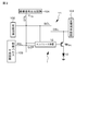
発光部駆動用トランジスタTRDrvのゲート電極は、インバータ回路30の出力端に接続されている。また、発光部駆動用トランジスタTRDrvの一方のソース/ドレイン電極は、電流供給線CSLを介して、表示装置に備えられた定電流供給部101に接続されている。更には、発光部駆動用トランジスタTRDrvの他方のソース/ドレイン電極は、発光部10に接続されている。
The gate electrode of the light emitting unit driving transistor TR Drv is connected to the output terminal of the inverter circuit 30. Further, one source / drain electrode of the light emitting unit driving transistor TR Drv is connected to a constant current supply unit 101 provided in the display device via a current supply line CSL. Further, the other source / drain electrode of the light emitting unit driving transistor TR Drv is connected to the light emitting unit 10.
容量部C1の他端は、インバータ回路30の入力端(入力ノード)に接続されている。また、発光部10は発光ダイオードから成る。尚、定電流供給部101、走査回路102、制御パルス生成回路103、画像信号出力回路104等は、表示装置に配設されていてもよいし、外部に配設されていてもよい。
The other end of the capacitance unit C 1 is connected to an input end (input node) of the inverter circuit 30. The light emitting unit 10 is made of a light emitting diode. The constant current supply unit 101, the scanning circuit 102, the control pulse generation circuit 103, the image signal output circuit 104, and the like may be provided in the display device or may be provided outside.
また、走査線SCLを通して与えられる走査信号が高レベルになるときには、インバータ14を介した走査信号の反転信号に応答して、制御部35を構成する第2スイッチ回路(pチャネル型電界効果トランジスタTR18)がオン状態になる。これにより、1段目のCMOSインバータ31が第2スイッチ回路(pチャネル型電界効果トランジスタTR18)を通して高電位側の電源Vddに接続されるため、コンパレータ装置12が作動状態となる。その結果、制御パルスLCPの高レベル区間であっても、コンパレータ装置12を作動させる必要があるときには、コンパレータ装置12を確実に作動状態とすることができる。
Further, when the scanning signal supplied through the scanning line SCL becomes high level, the second switch circuit (p-channel field effect transistor TR) constituting the control unit 35 in response to the inverted signal of the scanning signal through the inverter 14. 18 ) is turned on. As a result, the first-stage CMOS inverter 31 is connected to the power source V dd on the high potential side through the second switch circuit (p-channel field effect transistor TR 18 ), so that the comparator device 12 is activated. As a result, even in the high level section of the control pulse LCP, when the comparator device 12 needs to be operated, the comparator device 12 can be reliably brought into an operating state.
定電流源42は、例えばpチャネル型電界効果トランジスタTR27によって構成されている。pチャネル型電界効果トランジスタTR27のゲート電極に、定電圧回路43で生成される一定の電圧が印加されることで、定電流源42は差動回路41に対して定電流を供給する。定電圧回路43は、例えば、高電位側の電源Vddと低電位側の電源GNDとの間に直列に接続された、pチャネル型電界効果トランジスタTR31,TR32、及び、nチャネル型電界効果トランジスタTR33,TR34から成る。尚、pチャネル型電界効果トランジスタTR32 及びnチャネル型電界効果トランジスタTR33,TR34は、ゲート電極とドレイン電極とが共通に接続されたダイオード接続構成となっている。
The constant current source 42 is constituted for example by a p-channel type field effect transistor TR 27. The constant current source 42 supplies a constant current to the differential circuit 41 by applying a constant voltage generated by the constant voltage circuit 43 to the gate electrode of the p-channel field effect transistor TR 27 . The constant voltage circuit 43 includes, for example, p-channel field effect transistors TR 31 and TR 32 and an n-channel electric field that are connected in series between the high-potential power supply V dd and the low-potential power supply GND. It comprises effect transistors TR 33 and TR 34 . The p-channel field effect transistor TR 32 and the n-channel field effect transistors TR 33 and TR 34 have a diode connection configuration in which a gate electrode and a drain electrode are connected in common.
差動回路41において、pチャネル型電界効果トランジスタTR22のドレイン電極とnチャネル型電界効果トランジスタTR24のドレイン電極との共通接続点(ノード)が、出力端(出力ノード)となる。この出力端には、ソース接地回路44の入力端が接続されている。ソース接地回路44は、高電位側の電源Vddと低電位側の電源GNDとの間に直列に接続された、pチャネル型電界効果トランジスタTR25と、nチャネル型電界効果トランジスタTR26とから成り、電界効果トランジスタTR25のゲート電極には定電圧回路43から一定の電圧が印加され、電界効果トランジスタTR26のゲート電極が差動回路41の出力端に接続されている。
In the differential circuit 41, the common connection point of the drain electrodes of the n-channel type field effect transistor TR 24 of p-channel type field effect transistor TR 22 (node) is an output terminal (output node). The output terminal is connected to the input terminal of the source ground circuit 44. The source ground circuit 44 includes a p-channel field effect transistor TR 25 and an n-channel field effect transistor TR 26 connected in series between the high-potential-side power supply V dd and the low-potential-side power supply GND. Thus, a constant voltage is applied from the constant voltage circuit 43 to the gate electrode of the field effect transistor TR 25, and the gate electrode of the field effect transistor TR 26 is connected to the output terminal of the differential circuit 41.
図10に示した例において、信号電圧書込み期間にあっては、制御パルスLCPの電圧は、例えば、3ボルト以上である。従って、信号電圧書込み期間にあっては、コンパレータ装置12,12’は、出力部から第2の所定電圧(H)を出力するので、発光部駆動用トランジスタTRDrvはオフ状態にある。画素ブロック発光期間において、制御パルスLCPの電圧が下降し始め、制御パルスLCPの鋸波形の電圧が信号電圧VSigに基づく電位以下になると、コンパレータ装置12,12’は、出力部から第1の所定電圧(L)を出力する。その結果、発光部駆動用トランジスタTRDrvはオン状態となり、電流供給線CSLから発光部10に電流が供給され、発光部10が発光する。制御パルスLCPの電圧は約1ボルトまで下降し、次いで、上昇に転じる。そして、制御パルスLCPの鋸波形の電圧が信号電圧VSigに基づく電位を超えると、コンパレータ装置12,12’は、出力部から第2の所定電圧(H)を出力する。その結果、発光部駆動用トランジスタTRDrvはオフ状態となり、電流供給線CSLから発光部10への電流の供給が遮断され、発光部10は発光を中止する。即ち、信号電圧(発光強度信号)VSigに基づく電位が制御パルスLCPの鋸波形を切り取る時間の間のみ、発光部10を発光させることができる。そして、このときの発光部10の輝度は、切り取られる時間の長短に依存する。
In the example shown in FIG. 10, during the signal voltage writing period, the voltage of the control pulse LCP is, for example, 3 volts or more. Therefore, in the signal voltage writing period, the comparator devices 12 and 12 ′ output the second predetermined voltage (H) from the output unit, and thus the light emitting unit driving transistor TR Drv is in the off state. In the pixel block light emission period, when the voltage of the control pulse LCP starts to drop and the voltage of the sawtooth waveform of the control pulse LCP becomes equal to or lower than the potential based on the signal voltage V Sig , the comparator devices 12 and 12 ′ A predetermined voltage (L) is output. As a result, the light emitting unit driving transistor TR Drv is turned on, current is supplied from the current supply line CSL to the light emitting unit 10, and the light emitting unit 10 emits light. The voltage of the control pulse LCP drops to about 1 volt and then turns up. Then, the voltage of the sawtooth waveform of the control pulse LCP exceeds the potential based on the signal voltage V Sig, the comparator device 12, 12 'outputs a second predetermined voltage (H) from the output unit. As a result, the light emitting unit driving transistor TR Drv is turned off, the supply of current from the current supply line CSL to the light emitting unit 10 is cut off, and the light emitting unit 10 stops emitting light. That is, the light emitting unit 10 can emit light only during the time when the potential based on the signal voltage (light emission intensity signal) V Sig cuts the sawtooth waveform of the control pulse LCP. And the brightness | luminance of the light emission part 10 at this time is dependent on the length of time to cut off.
尚、本開示は以下のような構成を取ることもできる。
[A01]《コンパレータ装置》
制御パルスと信号電圧に基づく電位とを比較する比較部、及び、
制御パルスによって比較部の作動/不作動を制御する制御部、
を備えるコンパレータ装置。
[A02]《コンパレータ装置:第1の構成》
比較部は、
信号電圧が入力される信号書込みトランジスタ、
制御パルスが入力され、信号書込みトランジスタと逆相の信号でオン/オフ動作を行う制御パルス用トランジスタ、
インバータ回路、並びに、
信号書込みトランジスタ及び制御パルス用トランジスタに一端が接続され、他端がインバータ回路に接続され、信号書込みトランジスタの作動に基づき、信号電圧に基づく電位を保持する容量部、
を有する[A01]に記載のコンパレータ装置。
[A03]制御パルスは、鋸波形の電圧変化を有し、
制御部は、インバータ回路に対して直列に接続され、制御パルスの鋸波形の電圧に応じてオン/オフ動作を行うスイッチ回路を有する[A02]に記載のコンパレータ装置。
[A04]制御部は、スイッチ回路に対して並列に接続され、コンパレータ装置の作動期間でオン状態になる第2スイッチ回路を有する[A03]に記載のコンパレータ装置。
[A05]制御部は、インバータ回路に対して直列に接続された抵抗要素を有する[A03]又は[A04]に記載のコンパレータ装置。
[A06]制御部は、インバータ回路に対して直列に接続され、インバータ回路に流れる電流を抑える定電流源を有する[A03]乃至[A05]のいずれか1項に記載のコンパレータ装置。
[A07]インバータ回路は、インバータが、少なくとも2段縦続接続されて成り、
定電流源は、1段目のインバータに対して高電位側/低電位側の電源の一方の側に接続され、2段目のインバータに対して高電位側/低電位側の電源の他方の側に接続されている[A06]に記載のコンパレータ装置。
[A08]《コンパレータ装置:第2の構成》
比較部は、
信号電圧と制御パルスとを2入力とする差動回路、及び、
差動回路に定電流を供給する定電流源、
を有する[A01]に記載のコンパレータ装置。
[A09]]比較部は、更に、
信号電圧が入力される信号書込みトランジスタ、及び、
信号書込みトランジスタに接続され、信号書込みトランジスタの作動に基づき、信号電圧に基づく電位を保持する容量部、
を有する[A08]に記載のコンパレータ装置。
[A10]制御パルスは、鋸波形の電圧変化を有し、
制御部は、定電流源に対して直列に接続され、制御パルスの鋸波形の電圧に応じてオン/オフ動作を行うスイッチ回路を有する[A08]又は[A09]に記載のコンパレータ装置。
[A11]制御部は、定電流源を構成するトランジスタのゲート電極に定電圧を与える定電圧回路に対して直列に接続され、制御パルスの鋸波形の電圧に応じてオン/オフ動作を行う第2スイッチ回路を有する[A10]に記載のコンパレータ装置。
[B01]《表示装置》
発光部、及び、発光部を駆動する駆動回路から構成された画素が、複数、2次元マトリクス状に配列されて成り、
各駆動回路は、
制御パルスと信号電圧に基づく電位とを比較し、比較結果に基づく所定電圧を出力するコンパレータ装置、並びに、
コンパレータ装置からの所定電圧に応じて発光部に電流を供給し、発光部を発光させる発光部駆動用トランジスタ、
を備えており、
コンパレータ装置は、
制御パルスと信号電圧に基づく電位とを比較する比較部、及び、
制御パルスによって比較部の作動/不作動を制御する制御部、
を備えている表示装置。
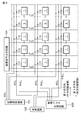
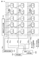
[B02]複数の画素は、第1の方向及び第2の方向に2次元マトリクス状に配列され、画素群は第1の方向に沿ってP個の画素ブロックに分割されており、
第1番目の画素ブロックに属する画素を構成する発光部から、第P番目の画素ブロックに属する画素を構成する発光部まで、画素ブロック毎に、順次、一斉に発光させ、且つ、一部の画素ブロックに属する画素を構成する発光部を発光させているとき、残りの画素ブロックに属する画素を構成する発光部を発光させないように構成された[B01]に記載の表示装置。
[B03]複数の制御パルスに基づき、発光部が、複数回、発光する[B01]又は[B02]に記載の表示装置。
[B04]複数の制御パルスの時間間隔は一定である[B03]に記載の表示装置。
[B05]1表示フレーム内における制御パルスの数よりも、1表示フレーム内における駆動回路に供給される制御パルスの数は少ない[B01]乃至[B04]のいずれか1項に記載の表示装置。
[B06]1表示フレームにおいて、常に、いずれかの画素ブロックが発光している[B01]乃至[B05]のいずれか1項に記載の表示装置。
[B07]1表示フレームにおいて、発光していない画素ブロックが存在する[B01]乃至[B05]のいずれか1項に記載の表示装置。
[B08]鋸波形の電圧変化を有する制御パルスを生成する制御パルス生成回路を1つ備えている[B01]乃至[B07]のいずれか1項に記載の表示装置。
[B09]1つの制御パルスの電圧の絶対値は、時間の経過と共に、増加し、次いで、減少する[B01]乃至[B08]のいずれか1項に記載の表示装置。
[B10]時間の経過と共に変化する制御パルスの電圧によってガンマ補正がなされる[B09]に記載の表示装置。
[B11]時間を変数とした制御パルスの電圧の変化率の絶対値は、定数2.2に比例する[B10]に記載の表示装置。
[B12]発光部は発光ダイオードから構成されている[B01]乃至[B11]のいずれか1項に記載の表示装置。
[B13]《表示装置:第1の構成》
比較部は、
信号電圧が入力される信号書込みトランジスタ、
制御パルスが入力され、信号書込みトランジスタと逆相の信号でオン/オフ動作を行う制御パルス用トランジスタ、
インバータ回路、並びに、
信号書込みトランジスタ及び制御パルス用トランジスタに一端が接続され、他端がインバータ回路に接続され、信号書込みトランジスタの作動に基づき、信号電圧に基づく電位を保持する容量部、
を有する[B01]乃至[B12]のいずれか1項に記載の表示装置。
[B14]制御パルスは、鋸波形の電圧変化を有し、
制御部は、インバータ回路に対して直列に接続され、制御パルスの鋸波形の電圧に応じてオン/オフ動作を行うスイッチ回路を有する[B13]に記載の表示装置。
[B15]制御部は、スイッチ回路に対して並列に接続され、コンパレータ装置の作動期間でオン状態になる第2スイッチ回路を有する[B14]に記載の表示装置。
[B16]制御部は、インバータ回路に対して直列に接続された抵抗要素を有する[B14]又は[B15]に記載の表示装置。
[B17]制御部は、インバータ回路に対して直列に接続され、インバータ回路に流れる電流を抑える定電流源を有する[B14]乃至[B16]のいずれか1項に記載の表示装置。
[B18]インバータ回路は、インバータが、少なくとも2段縦続接続されて成り、
定電流源は、1段目のインバータに対して高電位側/低電位側の電源の一方の側に接続され、2段目のインバータに対して高電位側/低電位側の電源の他方の側に接続されている[B17]に記載の表示装置。
[B19]《表示装置:第2の構成》
比較部は、
信号電圧と制御パルスとを2入力とする差動回路、及び、
差動回路に定電流を供給する定電流源、
を有する[B01]乃至[B12]のいずれか1項に記載の表示装置。
[B20]]比較部は、更に、
信号電圧が入力される信号書込みトランジスタ、及び、
信号書込みトランジスタに接続され、信号書込みトランジスタの作動に基づき、信号電圧に基づく電位を保持する容量部、
を有する[B19]に記載の表示装置。
[B21]制御パルスは、鋸波形の電圧変化を有し、
制御部は、定電流源に対して直列に接続され、制御パルスの鋸波形の電圧に応じてオン/オフ動作を行うスイッチ回路を有する[B19]又は[B20]に記載の表示装置。
[B22]制御部は、定電流源を構成するトランジスタのゲート電極に定電圧を与える定電圧回路に対して直列に接続され、制御パルスの鋸波形の電圧に応じてオン/オフ動作を行う第2スイッチ回路を有する[B21]に記載の表示装置。
[B23]各画素ブロックにおいて、第2の方向に配列された1列に属する全ての画素における信号書込みトランジスタは、一斉に作動状態となる[B13]乃至[B22]のいずれか1項に記載の表示装置。
[B24]各画素ブロックにおいて、第2の方向に配列された1列に属する全ての画素における信号書込みトランジスタが一斉に作動状態となる動作が、第1の方向に配列された第1行目に属する全ての画素における信号書込みトランジスタから最終行に属する全ての画素における信号書込みトランジスタまで、順次、行われる[B23]に記載の表示装置。
[B25]各画素ブロックにおいて、第2の方向に配列された1列に属する全ての画素における信号書込みトランジスタが一斉に作動状態となる動作が、第1の方向に配列された第1行目に属する全ての画素における信号書込みトランジスタから最終行に属する全ての画素における信号書込みトランジスタまで、順次、行われた後、該画素ブロックに制御パルスが供給される[B24]に記載の表示装置。
[B26]第2の方向に配列された1列に属する画素は、制御パルス線に接続されており、
制御パルス線には、所定の間隔で、ボルテージフォロワー回路(バッファ回路)が配設されている[B01]乃至[B25]のいずれか1項に記載の表示装置。
[C01]《表示装置の駆動方法》
発光部、及び、発光部を駆動する駆動回路から構成された画素が、複数、2次元マトリクス状に配列されて成り、
各駆動回路は、
制御パルスと信号電圧に基づく電位とを比較し、比較結果に基づく所定電圧を出力するコンパレータ装置、並びに、
コンパレータ装置からの所定電圧に応じて発光部に電流を供給し、発光部を発光させる発光部駆動用トランジスタ、
を備えている表示装置の駆動方法であって、
制御パルスによってコンパレータ装置の作動/不作動を制御する表示装置の駆動方法。
In addition, this indication can also take the following structures.
[A01] << Comparator device >>
A comparison unit for comparing the control pulse and the potential based on the signal voltage; and
A control unit for controlling operation / non-operation of the comparison unit by a control pulse;
Comparator device comprising:
[A02] << Comparator device: first configuration >>
The comparison part
A signal writing transistor to which a signal voltage is input,
A control pulse transistor that is turned on / off by a signal having a phase opposite to that of the signal write transistor, to which a control pulse is input,
An inverter circuit, and
One end of the signal write transistor and the control pulse transistor is connected, the other end is connected to the inverter circuit, and based on the operation of the signal write transistor, a capacitor unit that holds a potential based on the signal voltage,
The comparator device according to [A01].
[A03] The control pulse has a sawtooth voltage change,
The control unit according to [A02], wherein the control unit includes a switch circuit that is connected in series to the inverter circuit and performs an on / off operation in accordance with a saw-tooth voltage of the control pulse.
[A04] The comparator unit according to [A03], wherein the control unit includes a second switch circuit that is connected in parallel to the switch circuit and is turned on during an operation period of the comparator device.
[A05] The comparator unit according to [A03] or [A04], wherein the control unit includes a resistance element connected in series to the inverter circuit.
[A06] The comparator unit according to any one of [A03] to [A05], wherein the control unit includes a constant current source that is connected in series to the inverter circuit and suppresses a current flowing through the inverter circuit.
[A07] The inverter circuit is formed by connecting the inverters in at least two stages,
The constant current source is connected to one side of the high-potential side / low-potential side power source with respect to the first stage inverter, and the other side of the high-potential side / low-potential side power source with respect to the second stage inverter The comparator device according to [A06] connected to the side.
[A08] << Comparator device: second configuration >>
The comparison part
A differential circuit having two inputs of a signal voltage and a control pulse; and
A constant current source for supplying a constant current to the differential circuit;
The comparator device according to [A01].
[A09]] The comparison unit further includes:
A signal writing transistor to which a signal voltage is input; and
A capacitor unit connected to the signal writing transistor and holding a potential based on the signal voltage based on the operation of the signal writing transistor;
The comparator device according to [A08], including:
[A10] The control pulse has a sawtooth voltage change,
The control unit is the comparator device according to [A08] or [A09], which includes a switch circuit that is connected in series to the constant current source and performs an on / off operation according to a voltage of a sawtooth waveform of the control pulse.
[A11] The control unit is connected in series to a constant voltage circuit that applies a constant voltage to the gate electrode of the transistor that constitutes the constant current source, and performs an on / off operation according to the voltage of the sawtooth waveform of the control pulse. The comparator device according to [A10], which includes a two-switch circuit.
[B01] << Display device >>
A plurality of pixels each composed of a light emitting unit and a driving circuit that drives the light emitting unit are arranged in a two-dimensional matrix,
Each drive circuit
A comparator device that compares a control pulse with a potential based on a signal voltage and outputs a predetermined voltage based on the comparison result; and
A light emitting unit driving transistor for supplying current to the light emitting unit in accordance with a predetermined voltage from the comparator device and causing the light emitting unit to emit light;
With
The comparator device
A comparison unit for comparing the control pulse and the potential based on the signal voltage; and
A control unit for controlling operation / non-operation of the comparison unit by a control pulse;
A display device comprising:
[B02] The plurality of pixels are arranged in a two-dimensional matrix in the first direction and the second direction, and the pixel group is divided into P pixel blocks along the first direction.
From a light emitting unit constituting a pixel belonging to the first pixel block to a light emitting unit constituting a pixel belonging to the Pth pixel block, light is emitted sequentially and simultaneously for each pixel block, and some pixels [B01] The display device according to [B01], configured to prevent the light emitting units constituting the pixels belonging to the remaining pixel blocks from emitting light when the light emitting units constituting the pixels belonging to the block emit light.
[B03] The display device according to [B01] or [B02], in which the light emitting unit emits light a plurality of times based on a plurality of control pulses.
[B04] The display device according to [B03], wherein time intervals of the plurality of control pulses are constant.
[B05] The display device according to any one of [B01] to [B04], wherein the number of control pulses supplied to the drive circuit in one display frame is smaller than the number of control pulses in one display frame.
[B06] The display device according to any one of [B01] to [B05], in which one of the pixel blocks always emits light in one display frame.
[B07] The display device according to any one of [B01] to [B05], wherein a pixel block that does not emit light exists in one display frame.
[B08] The display device according to any one of [B01] to [B07], including one control pulse generation circuit that generates a control pulse having a sawtooth waveform voltage change.
[B09] The display device according to any one of [B01] to [B08], in which the absolute value of the voltage of one control pulse increases with time and then decreases.
[B10] The display device according to [B09], in which gamma correction is performed by a voltage of a control pulse that changes with time.
[B11] The display device according to [B10], in which the absolute value of the rate of change of the voltage of the control pulse with time as a variable is proportional to the constant 2.2.
[B12] The display device according to any one of [B01] to [B11], in which the light-emitting portion includes a light-emitting diode.
[B13] << Display device : first configuration >>
The comparison part
A signal writing transistor to which a signal voltage is input,
A control pulse transistor that is turned on / off by a signal having a phase opposite to that of the signal write transistor, to which a control pulse is input,
An inverter circuit, and
One end of the signal write transistor and the control pulse transistor is connected, the other end is connected to the inverter circuit, and based on the operation of the signal write transistor, a capacitor unit that holds a potential based on the signal voltage,
The display device according to any one of [B01] to [B12].
[B14] The control pulse has a sawtooth voltage change,
The display unit according to [B13], wherein the control unit includes a switch circuit that is connected in series to the inverter circuit and that performs an on / off operation in accordance with a sawtooth voltage of the control pulse.
[B15] The display unit according to [B14], wherein the control unit includes a second switch circuit that is connected in parallel to the switch circuit and is turned on during an operation period of the comparator device.
[B16] The display unit according to [B14] or [B15], in which the control unit includes a resistance element connected in series to the inverter circuit.
[B17] The display unit according to any one of [B14] to [B16], wherein the control unit includes a constant current source that is connected in series to the inverter circuit and suppresses a current flowing through the inverter circuit.
[B18] The inverter circuit is formed by cascading at least two stages of inverters,
The constant current source is connected to one side of the high-potential side / low-potential side power source with respect to the first stage inverter, and the other side of the high-potential side / low-potential side power source with respect to the second stage inverter The display device according to [B17] connected to the side.
[B19] << Display device : second configuration >>
The comparison part
A differential circuit having two inputs of a signal voltage and a control pulse; and
A constant current source for supplying a constant current to the differential circuit;
The display device according to any one of [B01] to [B12].
[B20]] The comparison unit further includes:
A signal writing transistor to which a signal voltage is input; and
A capacitor unit connected to the signal writing transistor and holding a potential based on the signal voltage based on the operation of the signal writing transistor;
The display device according to [B19], including:
[B21] The control pulse has a sawtooth voltage change,
A control part is a display apparatus as described in [B19] or [B20] which has a switch circuit connected in series with respect to a constant current source, and performs ON / OFF operation | movement according to the voltage of the sawtooth waveform of a control pulse.
[B22] The control unit is connected in series to a constant voltage circuit that applies a constant voltage to the gate electrode of the transistor constituting the constant current source, and performs an on / off operation according to the voltage of the sawtooth waveform of the control pulse. The display device according to [B21], which includes a two-switch circuit.
[B23] In any one of [B13] to [B22], in each pixel block, the signal writing transistors in all the pixels belonging to one column arranged in the second direction are simultaneously activated. Display device.
[B24] In each pixel block, the operation in which the signal writing transistors in all the pixels belonging to one column arranged in the second direction are simultaneously activated is shown in the first row arranged in the first direction. [B23] The display device according to [B23], which is sequentially performed from the signal writing transistor in all the pixels belonging to the signal writing transistor in all the pixels belonging to the last row.
[B25] In each pixel block, the operation in which the signal write transistors in all the pixels belonging to one column arranged in the second direction are simultaneously activated is shown in the first row arranged in the first direction. The display device according to [B24], in which the control pulse is supplied to the pixel block after sequentially performing from the signal write transistor in all the pixels to the signal write transistor in all the pixels belonging to the last row.
[B26] Pixels belonging to one column arranged in the second direction are connected to a control pulse line,
The display device according to any one of [B01] to [B25], wherein a voltage follower circuit (buffer circuit) is disposed at a predetermined interval on the control pulse line.
[C01] << Driving method of display device >>
A plurality of pixels each composed of a light emitting unit and a driving circuit that drives the light emitting unit are arranged in a two-dimensional matrix,
Each drive circuit
A comparator device that compares a control pulse with a potential based on a signal voltage and outputs a predetermined voltage based on the comparison result; and
A light emitting unit driving transistor for supplying current to the light emitting unit in accordance with a predetermined voltage from the comparator device and causing the light emitting unit to emit light;
A driving method of a display device comprising:
A display device driving method for controlling operation / non-operation of a comparator device by a control pulse.