JP4651777B2 - Method for manufacturing semiconductor device - Google Patents
Method for manufacturing semiconductor device Download PDFInfo
- Publication number
- JP4651777B2 JP4651777B2 JP2000165617A JP2000165617A JP4651777B2 JP 4651777 B2 JP4651777 B2 JP 4651777B2 JP 2000165617 A JP2000165617 A JP 2000165617A JP 2000165617 A JP2000165617 A JP 2000165617A JP 4651777 B2 JP4651777 B2 JP 4651777B2
- Authority
- JP
- Japan
- Prior art keywords
- film
- insulating film
- interlayer insulating
- wiring
- gate
- Prior art date
- Legal status (The legal status is an assumption and is not a legal conclusion. Google has not performed a legal analysis and makes no representation as to the accuracy of the status listed.)
- Expired - Fee Related
Links
- 238000000034 method Methods 0.000 title claims description 62
- 239000004065 semiconductor Substances 0.000 title claims description 60
- 238000004519 manufacturing process Methods 0.000 title claims description 25
- 239000011229 interlayer Substances 0.000 claims description 138
- 239000010410 layer Substances 0.000 claims description 114
- 239000012535 impurity Substances 0.000 claims description 95
- 239000000758 substrate Substances 0.000 claims description 54
- 238000005530 etching Methods 0.000 claims description 43
- 239000010408 film Substances 0.000 description 479
- 239000013078 crystal Substances 0.000 description 49
- 239000004973 liquid crystal related substance Substances 0.000 description 49
- 239000011159 matrix material Substances 0.000 description 34
- 230000015572 biosynthetic process Effects 0.000 description 33
- 239000000463 material Substances 0.000 description 31
- OAICVXFJPJFONN-UHFFFAOYSA-N Phosphorus Chemical compound [P] OAICVXFJPJFONN-UHFFFAOYSA-N 0.000 description 24
- 239000003990 capacitor Substances 0.000 description 24
- 229910052698 phosphorus Inorganic materials 0.000 description 24
- 239000011574 phosphorus Substances 0.000 description 24
- XUIMIQQOPSSXEZ-UHFFFAOYSA-N Silicon Chemical compound [Si] XUIMIQQOPSSXEZ-UHFFFAOYSA-N 0.000 description 23
- 125000004429 atom Chemical group 0.000 description 23
- 229910052710 silicon Inorganic materials 0.000 description 23
- 239000010703 silicon Substances 0.000 description 23
- 238000010586 diagram Methods 0.000 description 21
- IJGRMHOSHXDMSA-UHFFFAOYSA-N Atomic nitrogen Chemical compound N#N IJGRMHOSHXDMSA-UHFFFAOYSA-N 0.000 description 20
- 229910021419 crystalline silicon Inorganic materials 0.000 description 20
- 238000010438 heat treatment Methods 0.000 description 20
- 229910052581 Si3N4 Inorganic materials 0.000 description 19
- 230000003071 parasitic effect Effects 0.000 description 19
- HQVNEWCFYHHQES-UHFFFAOYSA-N silicon nitride Chemical compound N12[Si]34N5[Si]62N3[Si]51N64 HQVNEWCFYHHQES-UHFFFAOYSA-N 0.000 description 19
- 239000012298 atmosphere Substances 0.000 description 17
- PXHVJJICTQNCMI-UHFFFAOYSA-N Nickel Chemical compound [Ni] PXHVJJICTQNCMI-UHFFFAOYSA-N 0.000 description 16
- 230000008569 process Effects 0.000 description 16
- VYPSYNLAJGMNEJ-UHFFFAOYSA-N Silicium dioxide Chemical compound O=[Si]=O VYPSYNLAJGMNEJ-UHFFFAOYSA-N 0.000 description 15
- 238000002425 crystallisation Methods 0.000 description 15
- 230000008025 crystallization Effects 0.000 description 15
- 238000007254 oxidation reaction Methods 0.000 description 15
- 230000003647 oxidation Effects 0.000 description 14
- 238000003860 storage Methods 0.000 description 14
- 230000003287 optical effect Effects 0.000 description 13
- 229910052760 oxygen Inorganic materials 0.000 description 13
- ZOXJGFHDIHLPTG-UHFFFAOYSA-N Boron Chemical compound [B] ZOXJGFHDIHLPTG-UHFFFAOYSA-N 0.000 description 12
- QVGXLLKOCUKJST-UHFFFAOYSA-N atomic oxygen Chemical compound [O] QVGXLLKOCUKJST-UHFFFAOYSA-N 0.000 description 12
- 229910052796 boron Inorganic materials 0.000 description 12
- 239000001301 oxygen Substances 0.000 description 12
- 229920005989 resin Polymers 0.000 description 12
- 239000011347 resin Substances 0.000 description 12
- 230000006870 function Effects 0.000 description 11
- 239000007789 gas Substances 0.000 description 11
- 229910052739 hydrogen Inorganic materials 0.000 description 11
- 239000001257 hydrogen Substances 0.000 description 11
- 229910052814 silicon oxide Inorganic materials 0.000 description 11
- XLOMVQKBTHCTTD-UHFFFAOYSA-N Zinc monoxide Chemical compound [Zn]=O XLOMVQKBTHCTTD-UHFFFAOYSA-N 0.000 description 10
- 229910052782 aluminium Inorganic materials 0.000 description 10
- XAGFODPZIPBFFR-UHFFFAOYSA-N aluminium Chemical compound [Al] XAGFODPZIPBFFR-UHFFFAOYSA-N 0.000 description 10
- 229910052757 nitrogen Inorganic materials 0.000 description 10
- UFHFLCQGNIYNRP-UHFFFAOYSA-N Hydrogen Chemical compound [H][H] UFHFLCQGNIYNRP-UHFFFAOYSA-N 0.000 description 9
- 239000010936 titanium Substances 0.000 description 9
- 229910021417 amorphous silicon Inorganic materials 0.000 description 8
- 238000000137 annealing Methods 0.000 description 8
- 230000007547 defect Effects 0.000 description 8
- 238000001312 dry etching Methods 0.000 description 8
- 229910003437 indium oxide Inorganic materials 0.000 description 8
- PJXISJQVUVHSOJ-UHFFFAOYSA-N indium(iii) oxide Chemical compound [O-2].[O-2].[O-2].[In+3].[In+3] PJXISJQVUVHSOJ-UHFFFAOYSA-N 0.000 description 8
- 229910052759 nickel Inorganic materials 0.000 description 8
- 238000000059 patterning Methods 0.000 description 8
- 238000001994 activation Methods 0.000 description 7
- 230000003197 catalytic effect Effects 0.000 description 7
- 150000001875 compounds Chemical class 0.000 description 7
- 239000005262 ferroelectric liquid crystals (FLCs) Substances 0.000 description 7
- 238000005268 plasma chemical vapour deposition Methods 0.000 description 7
- 229910021420 polycrystalline silicon Inorganic materials 0.000 description 7
- 229920005591 polysilicon Polymers 0.000 description 7
- 230000004044 response Effects 0.000 description 7
- 238000004544 sputter deposition Methods 0.000 description 7
- 230000000694 effects Effects 0.000 description 6
- 238000005247 gettering Methods 0.000 description 6
- 238000002347 injection Methods 0.000 description 6
- 239000007924 injection Substances 0.000 description 6
- 238000002161 passivation Methods 0.000 description 6
- 125000006850 spacer group Chemical group 0.000 description 6
- 238000001039 wet etching Methods 0.000 description 6
- 239000000945 filler Substances 0.000 description 5
- 238000005984 hydrogenation reaction Methods 0.000 description 5
- 150000002500 ions Chemical class 0.000 description 5
- 230000001681 protective effect Effects 0.000 description 5
- 238000005070 sampling Methods 0.000 description 5
- 239000003566 sealing material Substances 0.000 description 5
- 239000000243 solution Substances 0.000 description 5
- XOLBLPGZBRYERU-UHFFFAOYSA-N tin dioxide Chemical compound O=[Sn]=O XOLBLPGZBRYERU-UHFFFAOYSA-N 0.000 description 5
- 229910001887 tin oxide Inorganic materials 0.000 description 5
- 239000011787 zinc oxide Substances 0.000 description 5
- XYFCBTPGUUZFHI-UHFFFAOYSA-N Phosphine Chemical compound P XYFCBTPGUUZFHI-UHFFFAOYSA-N 0.000 description 4
- BLRPTPMANUNPDV-UHFFFAOYSA-N Silane Chemical compound [SiH4] BLRPTPMANUNPDV-UHFFFAOYSA-N 0.000 description 4
- RTAQQCXQSZGOHL-UHFFFAOYSA-N Titanium Chemical compound [Ti] RTAQQCXQSZGOHL-UHFFFAOYSA-N 0.000 description 4
- NIXOWILDQLNWCW-UHFFFAOYSA-N acrylic acid group Chemical group C(C=C)(=O)O NIXOWILDQLNWCW-UHFFFAOYSA-N 0.000 description 4
- 230000004913 activation Effects 0.000 description 4
- 239000010407 anodic oxide Substances 0.000 description 4
- QVQLCTNNEUAWMS-UHFFFAOYSA-N barium oxide Chemical compound [Ba]=O QVQLCTNNEUAWMS-UHFFFAOYSA-N 0.000 description 4
- 239000002585 base Substances 0.000 description 4
- 239000000969 carrier Substances 0.000 description 4
- -1 disilane Chemical compound 0.000 description 4
- 230000001747 exhibiting effect Effects 0.000 description 4
- 238000007667 floating Methods 0.000 description 4
- 238000005468 ion implantation Methods 0.000 description 4
- 239000000203 mixture Substances 0.000 description 4
- 229920003023 plastic Polymers 0.000 description 4
- 239000004033 plastic Substances 0.000 description 4
- 229920001721 polyimide Polymers 0.000 description 4
- 239000010453 quartz Substances 0.000 description 4
- 229910052719 titanium Inorganic materials 0.000 description 4
- 238000004627 transmission electron microscopy Methods 0.000 description 4
- 229910052721 tungsten Inorganic materials 0.000 description 4
- 239000010937 tungsten Substances 0.000 description 4
- LYCAIKOWRPUZTN-UHFFFAOYSA-N Ethylene glycol Chemical compound OCCO LYCAIKOWRPUZTN-UHFFFAOYSA-N 0.000 description 3
- GYHNNYVSQQEPJS-UHFFFAOYSA-N Gallium Chemical compound [Ga] GYHNNYVSQQEPJS-UHFFFAOYSA-N 0.000 description 3
- 239000004642 Polyimide Substances 0.000 description 3
- 229910045601 alloy Inorganic materials 0.000 description 3
- 239000000956 alloy Substances 0.000 description 3
- 230000005540 biological transmission Effects 0.000 description 3
- 238000005401 electroluminescence Methods 0.000 description 3
- 229910052733 gallium Inorganic materials 0.000 description 3
- 239000011521 glass Substances 0.000 description 3
- 238000005224 laser annealing Methods 0.000 description 3
- 229910052751 metal Inorganic materials 0.000 description 3
- 239000002184 metal Substances 0.000 description 3
- 229910021421 monocrystalline silicon Inorganic materials 0.000 description 3
- 230000000737 periodic effect Effects 0.000 description 3
- 239000012071 phase Substances 0.000 description 3
- 230000010287 polarization Effects 0.000 description 3
- 229920002620 polyvinyl fluoride Polymers 0.000 description 3
- 239000000565 sealant Substances 0.000 description 3
- 238000000926 separation method Methods 0.000 description 3
- 239000002356 single layer Substances 0.000 description 3
- 229910052715 tantalum Inorganic materials 0.000 description 3
- GUVRBAGPIYLISA-UHFFFAOYSA-N tantalum atom Chemical compound [Ta] GUVRBAGPIYLISA-UHFFFAOYSA-N 0.000 description 3
- MZLGASXMSKOWSE-UHFFFAOYSA-N tantalum nitride Chemical compound [Ta]#N MZLGASXMSKOWSE-UHFFFAOYSA-N 0.000 description 3
- 239000010409 thin film Substances 0.000 description 3
- 238000002834 transmittance Methods 0.000 description 3
- 238000007740 vapor deposition Methods 0.000 description 3
- 239000012808 vapor phase Substances 0.000 description 3
- 229920002799 BoPET Polymers 0.000 description 2
- RYGMFSIKBFXOCR-UHFFFAOYSA-N Copper Chemical compound [Cu] RYGMFSIKBFXOCR-UHFFFAOYSA-N 0.000 description 2
- 238000004435 EPR spectroscopy Methods 0.000 description 2
- XEEYBQQBJWHFJM-UHFFFAOYSA-N Iron Chemical compound [Fe] XEEYBQQBJWHFJM-UHFFFAOYSA-N 0.000 description 2
- WHXSMMKQMYFTQS-UHFFFAOYSA-N Lithium Chemical compound [Li] WHXSMMKQMYFTQS-UHFFFAOYSA-N 0.000 description 2
- 239000005041 Mylar™ Substances 0.000 description 2
- KDLHZDBZIXYQEI-UHFFFAOYSA-N Palladium Chemical compound [Pd] KDLHZDBZIXYQEI-UHFFFAOYSA-N 0.000 description 2
- 229910020286 SiOxNy Inorganic materials 0.000 description 2
- BOTDANWDWHJENH-UHFFFAOYSA-N Tetraethyl orthosilicate Chemical compound CCO[Si](OCC)(OCC)OCC BOTDANWDWHJENH-UHFFFAOYSA-N 0.000 description 2
- 230000009471 action Effects 0.000 description 2
- PNEYBMLMFCGWSK-UHFFFAOYSA-N aluminium oxide Inorganic materials [O-2].[O-2].[O-2].[Al+3].[Al+3] PNEYBMLMFCGWSK-UHFFFAOYSA-N 0.000 description 2
- 238000004458 analytical method Methods 0.000 description 2
- 230000008901 benefit Effects 0.000 description 2
- UMIVXZPTRXBADB-UHFFFAOYSA-N benzocyclobutene Chemical compound C1=CC=C2CCC2=C1 UMIVXZPTRXBADB-UHFFFAOYSA-N 0.000 description 2
- DQXBYHZEEUGOBF-UHFFFAOYSA-N but-3-enoic acid;ethene Chemical compound C=C.OC(=O)CC=C DQXBYHZEEUGOBF-UHFFFAOYSA-N 0.000 description 2
- 239000003054 catalyst Substances 0.000 description 2
- 238000005229 chemical vapour deposition Methods 0.000 description 2
- 239000011651 chromium Substances 0.000 description 2
- 238000000576 coating method Methods 0.000 description 2
- 238000011109 contamination Methods 0.000 description 2
- 229910052802 copper Inorganic materials 0.000 description 2
- 239000010949 copper Substances 0.000 description 2
- 230000007423 decrease Effects 0.000 description 2
- 230000006866 deterioration Effects 0.000 description 2
- 239000005038 ethylene vinyl acetate Substances 0.000 description 2
- 239000011152 fibreglass Substances 0.000 description 2
- 238000002173 high-resolution transmission electron microscopy Methods 0.000 description 2
- 150000002431 hydrogen Chemical class 0.000 description 2
- 229910010272 inorganic material Inorganic materials 0.000 description 2
- 239000011147 inorganic material Substances 0.000 description 2
- 239000012212 insulator Substances 0.000 description 2
- 229910052744 lithium Inorganic materials 0.000 description 2
- 238000004518 low pressure chemical vapour deposition Methods 0.000 description 2
- 239000012299 nitrogen atmosphere Substances 0.000 description 2
- 230000001590 oxidative effect Effects 0.000 description 2
- 229910000073 phosphorus hydride Inorganic materials 0.000 description 2
- 238000002294 plasma sputter deposition Methods 0.000 description 2
- 238000009832 plasma treatment Methods 0.000 description 2
- BASFCYQUMIYNBI-UHFFFAOYSA-N platinum Chemical compound [Pt] BASFCYQUMIYNBI-UHFFFAOYSA-N 0.000 description 2
- 229920001200 poly(ethylene-vinyl acetate) Polymers 0.000 description 2
- 229920002037 poly(vinyl butyral) polymer Polymers 0.000 description 2
- 229920006267 polyester film Polymers 0.000 description 2
- 229920000915 polyvinyl chloride Polymers 0.000 description 2
- 239000004800 polyvinyl chloride Substances 0.000 description 2
- 238000012545 processing Methods 0.000 description 2
- 230000009467 reduction Effects 0.000 description 2
- 229910000077 silane Inorganic materials 0.000 description 2
- 238000009751 slip forming Methods 0.000 description 2
- 238000004528 spin coating Methods 0.000 description 2
- 239000010935 stainless steel Substances 0.000 description 2
- 229910001220 stainless steel Inorganic materials 0.000 description 2
- 239000000126 substance Substances 0.000 description 2
- 238000002230 thermal chemical vapour deposition Methods 0.000 description 2
- WFKWXMTUELFFGS-UHFFFAOYSA-N tungsten Chemical compound [W] WFKWXMTUELFFGS-UHFFFAOYSA-N 0.000 description 2
- 235000012431 wafers Nutrition 0.000 description 2
- IUOOGQJPAJDLFV-UHFFFAOYSA-N 2,3-dihydroxybutanedioic acid;ethane-1,2-diol Chemical compound OCCO.OC(=O)C(O)C(O)C(O)=O IUOOGQJPAJDLFV-UHFFFAOYSA-N 0.000 description 1
- YLYPIBBGWLKELC-RMKNXTFCSA-N 2-[2-[(e)-2-[4-(dimethylamino)phenyl]ethenyl]-6-methylpyran-4-ylidene]propanedinitrile Chemical compound C1=CC(N(C)C)=CC=C1\C=C\C1=CC(=C(C#N)C#N)C=C(C)O1 YLYPIBBGWLKELC-RMKNXTFCSA-N 0.000 description 1
- DDFHBQSCUXNBSA-UHFFFAOYSA-N 5-(5-carboxythiophen-2-yl)thiophene-2-carboxylic acid Chemical compound S1C(C(=O)O)=CC=C1C1=CC=C(C(O)=O)S1 DDFHBQSCUXNBSA-UHFFFAOYSA-N 0.000 description 1
- 239000004925 Acrylic resin Substances 0.000 description 1
- 229920000178 Acrylic resin Polymers 0.000 description 1
- 229910001316 Ag alloy Inorganic materials 0.000 description 1
- VHUUQVKOLVNVRT-UHFFFAOYSA-N Ammonium hydroxide Chemical compound [NH4+].[OH-] VHUUQVKOLVNVRT-UHFFFAOYSA-N 0.000 description 1
- OKTJSMMVPCPJKN-UHFFFAOYSA-N Carbon Chemical compound [C] OKTJSMMVPCPJKN-UHFFFAOYSA-N 0.000 description 1
- VYZAMTAEIAYCRO-UHFFFAOYSA-N Chromium Chemical compound [Cr] VYZAMTAEIAYCRO-UHFFFAOYSA-N 0.000 description 1
- VEXZGXHMUGYJMC-UHFFFAOYSA-N Hydrochloric acid Chemical compound Cl VEXZGXHMUGYJMC-UHFFFAOYSA-N 0.000 description 1
- FYYHWMGAXLPEAU-UHFFFAOYSA-N Magnesium Chemical compound [Mg] FYYHWMGAXLPEAU-UHFFFAOYSA-N 0.000 description 1
- 229910000861 Mg alloy Inorganic materials 0.000 description 1
- ZOKXTWBITQBERF-UHFFFAOYSA-N Molybdenum Chemical compound [Mo] ZOKXTWBITQBERF-UHFFFAOYSA-N 0.000 description 1
- 239000004952 Polyamide Substances 0.000 description 1
- NRCMAYZCPIVABH-UHFFFAOYSA-N Quinacridone Chemical compound N1C2=CC=CC=C2C(=O)C2=C1C=C1C(=O)C3=CC=CC=C3NC1=C2 NRCMAYZCPIVABH-UHFFFAOYSA-N 0.000 description 1
- BQCADISMDOOEFD-UHFFFAOYSA-N Silver Chemical compound [Ag] BQCADISMDOOEFD-UHFFFAOYSA-N 0.000 description 1
- 239000004990 Smectic liquid crystal Substances 0.000 description 1
- 241000862969 Stella Species 0.000 description 1
- 229910001362 Ta alloys Inorganic materials 0.000 description 1
- ATJFFYVFTNAWJD-UHFFFAOYSA-N Tin Chemical compound [Sn] ATJFFYVFTNAWJD-UHFFFAOYSA-N 0.000 description 1
- NRTOMJZYCJJWKI-UHFFFAOYSA-N Titanium nitride Chemical compound [Ti]#N NRTOMJZYCJJWKI-UHFFFAOYSA-N 0.000 description 1
- 229910001080 W alloy Inorganic materials 0.000 description 1
- LEVVHYCKPQWKOP-UHFFFAOYSA-N [Si].[Ge] Chemical compound [Si].[Ge] LEVVHYCKPQWKOP-UHFFFAOYSA-N 0.000 description 1
- 230000002411 adverse Effects 0.000 description 1
- 239000003513 alkali Substances 0.000 description 1
- 229910052783 alkali metal Inorganic materials 0.000 description 1
- 150000001340 alkali metals Chemical class 0.000 description 1
- 229910052784 alkaline earth metal Inorganic materials 0.000 description 1
- 150000001342 alkaline earth metals Chemical class 0.000 description 1
- 150000001408 amides Chemical class 0.000 description 1
- 235000011114 ammonium hydroxide Nutrition 0.000 description 1
- 238000002048 anodisation reaction Methods 0.000 description 1
- 238000007743 anodising Methods 0.000 description 1
- 239000007864 aqueous solution Substances 0.000 description 1
- 238000003491 array Methods 0.000 description 1
- 229910052785 arsenic Inorganic materials 0.000 description 1
- RQNWIZPPADIBDY-UHFFFAOYSA-N arsenic atom Chemical compound [As] RQNWIZPPADIBDY-UHFFFAOYSA-N 0.000 description 1
- NGPGDYLVALNKEG-UHFFFAOYSA-N azanium;azane;2,3,4-trihydroxy-4-oxobutanoate Chemical compound [NH4+].[NH4+].[O-]C(=O)C(O)C(O)C([O-])=O NGPGDYLVALNKEG-UHFFFAOYSA-N 0.000 description 1
- LDDQLRUQCUTJBB-UHFFFAOYSA-O azanium;hydrofluoride Chemical compound [NH4+].F LDDQLRUQCUTJBB-UHFFFAOYSA-O 0.000 description 1
- IVHJCRXBQPGLOV-UHFFFAOYSA-N azanylidynetungsten Chemical compound [W]#N IVHJCRXBQPGLOV-UHFFFAOYSA-N 0.000 description 1
- 229910052799 carbon Inorganic materials 0.000 description 1
- 239000010406 cathode material Substances 0.000 description 1
- 229910010293 ceramic material Inorganic materials 0.000 description 1
- 238000012512 characterization method Methods 0.000 description 1
- 238000006243 chemical reaction Methods 0.000 description 1
- 229910052804 chromium Inorganic materials 0.000 description 1
- 239000011248 coating agent Substances 0.000 description 1
- 229910017052 cobalt Inorganic materials 0.000 description 1
- 239000010941 cobalt Substances 0.000 description 1
- GUTLYIVDDKVIGB-UHFFFAOYSA-N cobalt atom Chemical compound [Co] GUTLYIVDDKVIGB-UHFFFAOYSA-N 0.000 description 1
- XCJYREBRNVKWGJ-UHFFFAOYSA-N copper(II) phthalocyanine Chemical compound [Cu+2].C12=CC=CC=C2C(N=C2[N-]C(C3=CC=CC=C32)=N2)=NC1=NC([C]1C=CC=CC1=1)=NC=1N=C1[C]3C=CC=CC3=C2[N-]1 XCJYREBRNVKWGJ-UHFFFAOYSA-N 0.000 description 1
- 238000000151 deposition Methods 0.000 description 1
- 230000008021 deposition Effects 0.000 description 1
- 238000001514 detection method Methods 0.000 description 1
- 238000011161 development Methods 0.000 description 1
- 239000010432 diamond Substances 0.000 description 1
- 229910003460 diamond Inorganic materials 0.000 description 1
- PZPGRFITIJYNEJ-UHFFFAOYSA-N disilane Chemical compound [SiH3][SiH3] PZPGRFITIJYNEJ-UHFFFAOYSA-N 0.000 description 1
- 239000004815 dispersion polymer Substances 0.000 description 1
- 238000009826 distribution Methods 0.000 description 1
- 238000010894 electron beam technology Methods 0.000 description 1
- 238000002003 electron diffraction Methods 0.000 description 1
- 238000005516 engineering process Methods 0.000 description 1
- 239000003822 epoxy resin Substances 0.000 description 1
- 238000001704 evaporation Methods 0.000 description 1
- 230000005669 field effect Effects 0.000 description 1
- 239000007850 fluorescent dye Substances 0.000 description 1
- 239000011888 foil Substances 0.000 description 1
- 229910052732 germanium Inorganic materials 0.000 description 1
- GNPVGFCGXDBREM-UHFFFAOYSA-N germanium atom Chemical compound [Ge] GNPVGFCGXDBREM-UHFFFAOYSA-N 0.000 description 1
- 229910052736 halogen Inorganic materials 0.000 description 1
- 150000002367 halogens Chemical class 0.000 description 1
- RBTKNAXYKSUFRK-UHFFFAOYSA-N heliogen blue Chemical compound [Cu].[N-]1C2=C(C=CC=C3)C3=C1N=C([N-]1)C3=CC=CC=C3C1=NC([N-]1)=C(C=CC=C3)C3=C1N=C([N-]1)C3=CC=CC=C3C1=N2 RBTKNAXYKSUFRK-UHFFFAOYSA-N 0.000 description 1
- 230000005525 hole transport Effects 0.000 description 1
- 229910000041 hydrogen chloride Inorganic materials 0.000 description 1
- IXCSERBJSXMMFS-UHFFFAOYSA-N hydrogen chloride Substances Cl.Cl IXCSERBJSXMMFS-UHFFFAOYSA-N 0.000 description 1
- 230000006872 improvement Effects 0.000 description 1
- AMGQUBHHOARCQH-UHFFFAOYSA-N indium;oxotin Chemical compound [In].[Sn]=O AMGQUBHHOARCQH-UHFFFAOYSA-N 0.000 description 1
- 239000011810 insulating material Substances 0.000 description 1
- 229910052742 iron Inorganic materials 0.000 description 1
- 238000005499 laser crystallization Methods 0.000 description 1
- 239000011133 lead Substances 0.000 description 1
- PQXKHYXIUOZZFA-UHFFFAOYSA-M lithium fluoride Chemical compound [Li+].[F-] PQXKHYXIUOZZFA-UHFFFAOYSA-M 0.000 description 1
- 239000011777 magnesium Substances 0.000 description 1
- 239000003550 marker Substances 0.000 description 1
- 238000005259 measurement Methods 0.000 description 1
- 239000007769 metal material Substances 0.000 description 1
- 239000011259 mixed solution Substances 0.000 description 1
- 230000004048 modification Effects 0.000 description 1
- 238000012986 modification Methods 0.000 description 1
- 229910052750 molybdenum Inorganic materials 0.000 description 1
- 239000011733 molybdenum Substances 0.000 description 1
- 239000000178 monomer Substances 0.000 description 1
- TWNQGVIAIRXVLR-UHFFFAOYSA-N oxo(oxoalumanyloxy)alumane Chemical compound O=[Al]O[Al]=O TWNQGVIAIRXVLR-UHFFFAOYSA-N 0.000 description 1
- BPUBBGLMJRNUCC-UHFFFAOYSA-N oxygen(2-);tantalum(5+) Chemical compound [O-2].[O-2].[O-2].[O-2].[O-2].[Ta+5].[Ta+5] BPUBBGLMJRNUCC-UHFFFAOYSA-N 0.000 description 1
- 229910052763 palladium Inorganic materials 0.000 description 1
- 125000002080 perylenyl group Chemical group C1(=CC=C2C=CC=C3C4=CC=CC5=CC=CC(C1=C23)=C45)* 0.000 description 1
- CSHWQDPOILHKBI-UHFFFAOYSA-N peryrene Natural products C1=CC(C2=CC=CC=3C2=C2C=CC=3)=C3C2=CC=CC3=C1 CSHWQDPOILHKBI-UHFFFAOYSA-N 0.000 description 1
- 239000002985 plastic film Substances 0.000 description 1
- 229920006255 plastic film Polymers 0.000 description 1
- 229910052697 platinum Inorganic materials 0.000 description 1
- 229920002647 polyamide Polymers 0.000 description 1
- 229920000647 polyepoxide Polymers 0.000 description 1
- 229920000642 polymer Polymers 0.000 description 1
- 230000002265 prevention Effects 0.000 description 1
- 239000002994 raw material Substances 0.000 description 1
- 230000008439 repair process Effects 0.000 description 1
- SBEQWOXEGHQIMW-UHFFFAOYSA-N silicon Chemical compound [Si].[Si] SBEQWOXEGHQIMW-UHFFFAOYSA-N 0.000 description 1
- HBMJWWWQQXIZIP-UHFFFAOYSA-N silicon carbide Chemical compound [Si+]#[C-] HBMJWWWQQXIZIP-UHFFFAOYSA-N 0.000 description 1
- 229910010271 silicon carbide Inorganic materials 0.000 description 1
- LIVNPJMFVYWSIS-UHFFFAOYSA-N silicon monoxide Chemical class [Si-]#[O+] LIVNPJMFVYWSIS-UHFFFAOYSA-N 0.000 description 1
- 229920002050 silicone resin Polymers 0.000 description 1
- 229910052709 silver Inorganic materials 0.000 description 1
- 239000004332 silver Substances 0.000 description 1
- 229910001936 tantalum oxide Inorganic materials 0.000 description 1
- 229920001187 thermosetting polymer Polymers 0.000 description 1
- 229910052718 tin Inorganic materials 0.000 description 1
- 239000011135 tin Substances 0.000 description 1
- 239000012780 transparent material Substances 0.000 description 1
- WQJQOUPTWCFRMM-UHFFFAOYSA-N tungsten disilicide Chemical compound [Si]#[W]#[Si] WQJQOUPTWCFRMM-UHFFFAOYSA-N 0.000 description 1
- 229910021342 tungsten silicide Inorganic materials 0.000 description 1
Images


Classifications
-
- H—ELECTRICITY
- H10—SEMICONDUCTOR DEVICES; ELECTRIC SOLID-STATE DEVICES NOT OTHERWISE PROVIDED FOR
- H10K—ORGANIC ELECTRIC SOLID-STATE DEVICES
- H10K59/00—Integrated devices, or assemblies of multiple devices, comprising at least one organic light-emitting element covered by group H10K50/00
- H10K59/80—Constructional details
- H10K59/8791—Arrangements for improving contrast, e.g. preventing reflection of ambient light
- H10K59/8792—Arrangements for improving contrast, e.g. preventing reflection of ambient light comprising light absorbing layers, e.g. black layers
-
- H—ELECTRICITY
- H01—ELECTRIC ELEMENTS
- H01L—SEMICONDUCTOR DEVICES NOT COVERED BY CLASS H10
- H01L2924/00—Indexing scheme for arrangements or methods for connecting or disconnecting semiconductor or solid-state bodies as covered by H01L24/00
- H01L2924/0001—Technical content checked by a classifier
- H01L2924/0002—Not covered by any one of groups H01L24/00, H01L24/00 and H01L2224/00
Landscapes
- Liquid Crystal (AREA)
- Thin Film Transistor (AREA)
- Recrystallisation Techniques (AREA)
- Devices For Indicating Variable Information By Combining Individual Elements (AREA)
- Drying Of Semiconductors (AREA)
- Internal Circuitry In Semiconductor Integrated Circuit Devices (AREA)
- Semiconductor Memories (AREA)
- Non-Volatile Memory (AREA)
Description
【0001】
【発明の属する技術分野】
本願発明は薄膜トランジスタ(以下、TFTという)で構成された回路を有する半導体装置およびその作製方法に関する。例えば、液晶表示パネルに代表される電気光学装置およびその様な電気光学装置を部品として搭載した電子機器に関する。
【0002】
なお、本明細書中において半導体装置とは、半導体特性を利用することで機能しうる装置全般を指し、電気光学装置、半導体回路および電子機器は全て半導体装置である。
【0003】
【従来の技術】
絶縁表面を有する基板上にTFTで形成した大面積集積回路を有する半導体装置の開発が進んでいる。アクティブマトリクス型液晶表示装置、EL表示装置、および密着型イメージセンサはその代表例として知られている。特に、結晶質シリコン膜(典型的にはポリシリコン膜)を活性層にしたTFT(以下、ポリシリコンTFTと記す)は電界効果移動度が高いことから、いろいろな機能回路を形成することも可能である。
【0004】
例えば、アクティブマトリクス型液晶表示装置には、機能ブロックごとに画像表示を行う画素回路や、CMOS回路を基本としたシフトレジスタ回路、レベルシフタ回路、バッファ回路、サンプリング回路などの画素回路を制御するための駆動回路が一枚の基板上に形成される。
【0005】
アクティブマトリクス型液晶表示装置の画素回路には、数十から数百万個の各画素にTFTが配置され、そのTFTのそれぞれには画素電極が設けられている。液晶を挟んだ対向基板側には対向電極が設けられており、液晶を誘電体とした一種のコンデンサを形成している。そして、各画素に印加する電圧をTFTのスイッチング機能により制御して、このコンデンサへの電荷を制御することで液晶を駆動し、透過光量を制御して画像を表示する仕組みになっている。
【0006】
【発明が解決しようとする課題】
絶縁表面上に画素回路及び駆動回路を形成した場合、形成される多層配線間で必然的に容量(寄生容量)が生じてしまう。
【0007】
この寄生容量の大きさは、下層配線と上層配線とが重なっている電極面積や、重なっている下層配線と上層配線との間の絶縁膜の膜厚等で決定される。
【0008】
近年、回路の小型化及び低電力化が進むにつれ、この寄生容量の影響が無視できないほど大きくなっている。そこで、この寄生容量の影響を低下させるために補助容量の電極面積を大きくすることが提案されているが、電極面積を大きくすると画素領域の開口率が低下するという問題があった。
【0009】
また、下層配線と上層配線とが重ならないようにすると、同様に画素領域の開口率が低下する。
【0010】
特に、対角1インチ以下のアクティブマトリクス型液晶表示装置においては、開口率が最も重要視されている。
【0011】
画素領域の開口率を向上させるためには、配線面積を抑えるために配線幅を小さくしたり、下層配線と上層配線を可能な限り重ねて多層配線を形成することが行われている。
【0012】
また、回路の小型化によってTFTのソース領域やドレイン領域に達するコンタクトホールの寸法も微細化されている。良好なコンタクト接続をとるためには、コンタクトホールをテーパー状に加工して傾斜を持たせるようにすればよいが、極端なテーパー形状加工を行うとコンタクトホールの寸法が大きくなってしまう。例えば0.5〜1.5μm程度の直径を有する微小なコンタクトホールを形成しようとした場合、TFTのソース領域やドレイン領域の膜厚は10nm〜50nmと薄いため、層間絶縁膜が厚いとエッチング条件によってはオーバーエッチングやエッチング残りなどのエッチング不良が発生していた。
【0013】
本発明はこのような課題を解決するための技術であり、多層配線間で形成される寄生容量を低減し、表示特性を向上させることを目的とする。また、そのような半導体装置を実現するための作製方法を提供することを課題とする。
【0014】
【課題を解決するための手段】
本明細書で開示する発明の構成は、
絶縁表面上に第1配線と、
前記第1配線を覆う第1層間絶縁膜と、
前記第1層間絶縁膜上の一部に接して第2層間絶縁膜と、
前記第1層間絶縁膜及び前記第2層間絶縁膜上に第2配線とを有し、
前記第1配線と前記第2配線とが重なっている領域には、前記第1層間絶縁膜と前記第2層間絶縁膜とが積層されていることを特徴とする半導体装置である。
【0015】
上記構成において、前記第1層間絶縁膜のエッチングレートは、前記第2層間絶縁膜のエッチングレートより小さいことを特徴としている。
【0016】
また、上記各構成において、前記第1層間絶縁膜の前記第2層間絶縁膜に対するエッチングレートの選択比は、1.5以上であることが望ましい。
【0017】
また、上記各構成において、前記第1層間絶縁膜の膜厚は50〜300nmであることを特徴としている。
【0018】
また、上記各構成において、前記第2層間絶縁膜の膜厚は150nm〜1μmであることを特徴としている。
【0019】
また、他の発明の構成は、
絶縁表面上にTFTを少なくとも含む半導体装置において、
前記TFTを形成する第1配線の上方には第1層間絶縁膜と、第2層間絶縁膜と、第2配線とが形成され、
前記TFTのソース領域またはドレイン領域の上方にはゲート絶縁膜と、第1層間絶縁膜と、前記第2配線とが形成されていることを特徴とする半導体装置である。
【0020】
上記構成において、前記ゲート絶縁膜の膜厚と前記第1層間絶縁膜の膜厚との和は0.1μm以上であることを特徴としている。
【0021】
また、他の発明の構成は、
絶縁表面上にTFTを少なくとも含む半導体装置において、
前記TFTを形成する第1配線の上方には第1層間絶縁膜及び第2層間絶縁膜を介して第2配線が存在していることを特徴とする半導体装置である。
【0022】
上記構成において、前記TFTのソース領域またはドレイン領域の上方には第1層間絶縁膜が存在していることを特徴としている。
【0023】
また、上記各構成において、前記TFTは逆スタガ型TFTであることを特徴としている。
【0024】
また、上記各構成において、前記第1配線はゲート配線である。
【0025】
また、他の発明の構成は、
同一基板上に画素回路と該画素回路を制御するための駆動回路とを少なくとも含む半導体装置において、
前記画素回路を形成する画素TFTのチャネル形成領域は、ゲート絶縁膜を介してゲート配線の一部と重なるように形成され、該ゲート配線の一部はエッチングレートの異なる複数の絶縁膜を介して第2配線と重なっていることを特徴とする半導体装置である。
【0026】
また、上記各構成において、前記第2配線はソース線またはドレイン線である。
【0027】
上記各構成において、前記駆動回路を形成するnチャネル型TFTのLDD領域は、少なくとも一部または全部が、該nチャネル型TFTのゲート配線と重なるように形成され、
前記画素回路を形成する画素TFTのLDD領域は、該画素TFTのゲート電極と重ならないように形成されていることを特徴としている。
【0028】
上記各構成において、前記駆動回路を形成するnチャネル型TFTのLDD領域は、少なくとも一部または全部が、該nチャネル型TFTのゲート電極と重なるように形成され、
前記画素回路を形成する画素TFTのLDD領域は、該画素TFTのゲート電極と重ならないように形成され、
前記画素回路の保持容量は有機樹脂膜の上に設けられた遮蔽膜、該遮蔽膜の酸化物および画素電極で形成されていることを特徴としている。
【0029】
また、上記構造を実現するための発明の構成は、
絶縁表面上に第1配線を形成する第1工程と、
前記第1配線を覆う第1層間絶縁膜を形成する第2工程と、
前記第1層間絶縁膜上に第2層間絶縁膜を形成する第3工程と、
前記第2層間絶縁膜の一部を選択的に除去する第4工程と、
前記第1配線と重なる第2層間絶縁膜上に第2配線を形成する第5工程とを有することを特徴とする半導体装置の作製方法である。
【0030】
また、他の発明の構成は、
絶縁表面上にTFTを少なくとも含む半導体装置の作製方法において、
絶縁表面上に活性層を形成する第1工程と、
前記活性層に接してゲート絶縁膜を形成する第2工程と、
前記活性層の一部にn型不純物元素またはp型不純物元素を添加してソース領域またはドレイン領域を形成する第3工程と、
ゲート配線及びゲート電極を覆う第1層間絶縁膜を形成する第4工程と、
前記第1層間絶縁膜上に第2層間絶縁膜を形成する第5工程と、
前記第2層間絶縁膜にエッチングを行い、前記ソース領域または前記ドレイン領域の上方の第2層間絶縁膜を除去する第6工程と、
前記第1層間絶縁膜及び前記ゲート絶縁膜にエッチングを行い、前記ソース領域またはドレイン領域に達するコンタクトホールを形成する第7工程と、
前記ゲート電極と重なる前記第2層間絶縁膜上に、前記ソース領域またはドレイン領域と接する第2配線を形成する第8工程とを有することを特徴とする半導体装置の作製方法である。
【0031】
また、他の発明の構成は、
同一基板上に画素回路と該画素回路を制御するための駆動回路とを少なくとも含む半導体装置の作製方法において、
絶縁表面上に活性層を形成する第1工程と、
前記活性層に接してゲート絶縁膜を形成する第2工程と、
前記ゲート絶縁膜上にゲート配線及びゲート電極を形成する第3工程と、
前記活性層の一部にn型不純物元素またはp型不純物元素を添加し、n型不純物領域またはp型不純物領域を形成する第4工程と、
ゲート配線及びゲート電極を覆う第1層間絶縁膜を形成する第5工程と、
前記ゲート電極と重なる第1層間絶縁膜上に第2層間絶縁膜を選択的に形成する第6工程と、
前記第1層間絶縁膜及び前記ゲート絶縁膜にエッチングを行い、前記n型不純物領域または前記p型不純物領域に達するコンタクトホールを形成する第7工程と、
前記ゲート電極と重なる前記第2層間絶縁膜上に、前記n型不純物領域または前記p型不純物領域と接する第2配線を形成する第8工程とを有することを特徴とする半導体装置の作製方法である。
【0032】
また、他の発明の構成は、
同一基板上に画素回路と該画素回路を制御するための駆動回路とを少なくとも含む半導体装置の作製方法において、
絶縁表面上に活性層を形成する第1工程と、
前記活性層に接してゲート絶縁膜を形成する第2工程と、
前記ゲート絶縁膜上にゲート配線及びゲート電極を形成する第3工程と、
前記活性層の一部にn型不純物元素またはp型不純物元素を添加し、n型不純物領域またはp型不純物領域を形成する第4工程と、
ゲート配線及びゲート電極を覆う第1層間絶縁膜を形成する第5工程と、
前記第1層間絶縁膜及び前記ゲート絶縁膜にエッチングを行い、前記n型不純物領域または前記p型不純物領域に達するコンタクトホールを形成する第6工程と、
前記第1層間絶縁膜上に第2層間絶縁膜を選択的に形成する第7工程と、
前記ゲート電極と重なる前記第2層間絶縁膜上に、前記n型不純物領域または前記p型不純物領域と接する第2配線を形成する第8工程とを有することを特徴とする半導体装置の作製方法である。
【0033】
【発明の実施の形態】
本願発明の実施形態について、図5を用いて以下に説明する。
【0034】
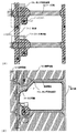
図5に示すように、本願発明では、開口率を向上させるため、画素TFTのチャネル形成領域213、214と重なるゲート電極の一部または全部と第2配線(ソース線またはドレイン線)154、157とを重ねる。また、ゲート電極と第2配線154、157の間には第1層間絶縁膜149及び第2層間絶縁膜150cを設け、寄生容量を低減する。なお、図8(B)に図5に対応する表示領域の上面図を示した。
【0035】
また、ゲート電極と第2配線が重なる領域のみに選択的に第2層間絶縁膜150cが設けられているため、画素TFTのソース領域またはドレイン領域に達するコンタクトホールの開口を行いやすい。
【0036】
また、駆動回路においては、絶縁膜115上に設けられたゲート配線と第2配線151とが交差して重なっている領域に第2層間絶縁膜150bを選択的に形成すればよい。なお、図7(B)に図5に対応する駆動回路の上面図を示した。
【0037】
なお、第1層間絶縁膜及び第2層間絶縁膜としては珪素を含む絶縁膜を用いる。珪素を含む絶縁膜としては、酸化シリコン膜、窒化シリコン膜、窒化酸化シリコン膜を用いることができる。これらの膜の成膜方法にはプラズマCVD、減圧CVD、ECRCVD等のCVD法や、スパッタ法等を用いればよい。なお、プラズマCVDを用い、原料ガスにSi源としてTEOS等の有機シランを、O源としてO2またはO3を用いればTEOS膜と呼ばれる絶縁膜が形成される。また、原料ガスにSi源としてSiH4(モノシラン)またはジシラン等の無機シランを用い、O源としてO2やO3やN2Oを用いることができる。なお、減圧CVD法を用い、Si源としてSiH4(モノシラン)、O源としてO2やO3やN2Oを用いればLTO膜と呼ばれる絶縁膜が形成される。
【0038】
なお、窒化酸化シリコン膜は、珪素、窒素及び酸素を所定の量で含む絶縁膜であり、SiOxNyで表される絶縁膜である。ただし、窒化酸化シリコン膜におけるSiの濃度に対するNの濃度比は0.1以上0.8以下にする。珪素、酸素、窒素等を含む絶縁膜の組成の制御は原料ガスの種類、流量、基板温度、圧力、RFパワー、電極間隔を適宜調節することによって行う。
【0039】
第1層間絶縁膜の膜厚は特に限定されないが、ゲート絶縁膜と同時または順次エッチングし、シリコン層に達するコンタクトホールを形成する際、シリコン層は薄いため、シリコン層と十分選択比が取れる条件(絶縁膜材料、膜厚、エッチングガス等)でエッチングを行うことが重要である。なお、これらの条件を考慮にいれると、第1層間絶縁膜の膜厚は薄くする(例えば200nm以下)ことが望ましい。ただし、活性化工程での酸化からゲート配線を保護する膜厚は必要である。また、微小なコンタクトホールを形成する上では、コンタクトホール形成領域に第2層間絶縁膜が存在しないようにすることが望ましい。
【0040】
また、上記構造を実現する本願発明の作製工程は、第2層間絶縁膜のみを選択的にウエットエッチングする工程(図4(B))を有しているため、第2層間絶縁膜に用いる材料は、第1層間絶縁膜よりもエッチングレートの大きな材料とすることが望ましい。
【0041】
第1層間絶縁膜と同じ原料ガスを用いて第2層間絶縁膜を成膜する場合でも、第1層間絶縁膜の成膜温度より10℃以上低い温度で成膜するとエッチングレートの大きな膜を得ることができる。
【0042】
また、第1層間絶縁膜に熱アニ―ル(750〜850℃、15分〜4時間)を施し、第1層間絶縁膜のエッチングレートを小さくすることによって、第2層間絶縁膜との選択比を大きくしてもよい。
【0043】
なお、第2層間絶縁膜のみを選択的にエッチングする工程の際、ドライエッチングを用いることは可能であるが、第1層間絶縁膜と選択比が十分取れ、テーパー形状が得られるウエットエッチングが望ましい。なお、第2層間絶縁膜の膜厚としては、寄生容量が問題にならない膜厚、例えば0.5μm以上であれば特に限定されない。また、異方性エッチングを用いてもよい。
【0044】
また、ソース領域またはドレイン領域に達するコンタクトホール形成の他の方法として、図12に示すようにドライエッチングでゲート絶縁膜及び第1層間絶縁膜にコンタクトホールを形成した後、第2層間絶縁膜を積層して再度、ウエットエッチングで第2層間絶縁膜にコンタクトホールを形成してもよい。
【0045】
また、第2層間絶縁膜のみを選択的にエッチングする工程として第1層間絶縁膜上に、薄い窒化シリコン膜や、DLC膜や、AlN膜、やAlNO膜等を積層し、それをエッチングのブロッキング層として用いればドライエッチングを用いて第2層間絶縁膜を選択的にエッチングすることができる。また、ドライエッチングを用いてもレジスト形状を変えればテーパー形状とすることができる。
【0046】
ここでは、ゲート配線と第2配線との間に2層の層間絶縁膜(第1層間絶縁膜及び第2層間絶縁膜)を用いたが、3層、あるいはそれ以上の層間絶縁膜を積層させてもよい。
【0047】
上記本願発明の構成とすることで、ゲート電極と第2配線とを重ねるレイアウトとしても寄生容量による表示特性への悪影響をなくすることができる。また、対角1インチ以下のアクティブマトリクス型液晶表示装置であっても、ゲート配線と第2配線とで形成される寄生容量が十分小さく、微小なコンタクトホール(直径が約0.5μm〜1.5μm)を形成することができる。
【0048】
以上の構成でなる本願発明について、以下に示す実施例でもってさらに詳細な説明を行うこととする。
【0049】
【実施例】
[実施例1]
本発明の実施例について図1〜図5を用いて説明する。ここでは、同一基板上に画素回路とその画素回路を制御するための駆動回路とを同時に作製する方法について説明する。但し、説明を簡単にするために、駆動回路では、シフトレジスタ回路、バッファ回路等の基本回路であるCMOS回路と、サンプリング回路を形成するnチャネル型TFTとを図示することとする。
【0050】
図1(A)において、基板101には、石英基板やシリコン基板を使用することが望ましい。本実施例では石英基板を用いた。その他にも金属基板またはステンレス基板の表面に絶縁膜を形成したものを基板としても良い。本実施例の場合、800℃以上の温度に耐えうる耐熱性を要求されるので、それを満たす基板であればどのような基板を用いても構わない。
【0051】
そして、基板101のTFTが形成される表面には、20〜100nm(好ましくは40〜80nm)の厚さの非晶質構造を含む半導体膜102を減圧熱CVD法、プラズマCVD法またはスパッタ法で形成する。なお、本実施例では60nm厚の非晶質シリコン膜を形成するが、後に熱酸化工程があるのでこの膜厚が最終的なTFTの活性層の膜厚になるわけではない。
【0052】
また、非晶質構造を含む半導体膜としては、非晶質半導体膜、微結晶半導体膜があり、さらに非晶質シリコンゲルマニウム膜などの非晶質構造を含む化合物半導体膜も含まれる。
【0053】
また、基板上に下地膜と非晶質シリコン膜とを大気解放しないで連続的に形成することも有効である。そうすることにより基板表面の汚染が非晶質シリコン膜に影響を与えないようにすることが可能となり、作製されるTFTの特性バラツキを低減させることができる。
【0054】
次に、非晶質シリコン膜102上に珪素(シリコン)を含む絶縁膜でなるマスク膜103を形成し、パターニングによって開口部104a、104bを形成する。この開口部は、次の結晶化工程の際に結晶化を助長する触媒元素を添加するための添加領域となる。(図1(A))
【0055】
なお、珪素を含む絶縁膜としては、酸化シリコン膜、窒化シリコン膜、窒化酸化シリコン膜を用いることができる。窒化酸化シリコン膜は、珪素、窒素及び酸素を所定の量で含む絶縁膜であり、SiOxNyで表される絶縁膜である。窒化酸化シリコン膜はSiH4、N2O及びNH3を原料ガスとして作製することが可能であり、含有する窒素濃度が25atomic%以上50atomic%未満とすると良い。
【0056】
また、このマスク膜103のパターニングを行うと同時に、後のパターニング工程の基準となるマーカーパターンを形成しておく。
【0057】
次に、特開平10−247735号公報(米国出願番号09/034,041に対応)に記載された技術に従って、結晶構造を含む半導体膜を形成する。同公報記載の技術は、非晶質構造を含む半導体膜の結晶化に際して、結晶化を助長する触媒元素(ニッケル、コバルト、ゲルマニウム、錫、鉛、パラジウム、鉄、銅から選ばれた一種または複数種の元素)を用いる結晶化手段である。
【0058】
具体的には、非晶質構造を含む半導体膜の表面に触媒元素を保持させた状態で加熱処理を行い、非晶質構造を含む半導体膜を、結晶構造を含む半導体膜に変化させるものである。なお、結晶化手段としては、特開平7−130652号公報の実施例1に記載された技術を用いても良い。また、結晶質構造を含む半導体膜には、いわゆる単結晶半導体膜も多結晶半導体膜も含まれるが、同公報で形成される結晶構造を含む半導体膜は結晶粒界を有している。
【0059】
なお、同公報では触媒元素を含む層をマスク膜上に形成する際にスピンコート法を用いているが、触媒元素を含む薄膜をスパッタ法や蒸着法といった気相法を用いて成膜する手段をとっても良い。
【0060】
また、非晶質シリコン膜は含有水素量にもよるが、好ましくは400〜550℃で1時間程度の加熱処理を行い、水素を十分に脱離させてから結晶化させることが望ましい。その場合、含有水素量を5atom%以下とすることが好ましい。
【0061】
結晶化工程は、まず400〜500℃で1時間程度の熱処理工程を行い、水素を膜中から脱離させた後、500〜650℃(好ましくは550〜600℃)で6〜16時間(好ましくは8〜14時間)の熱処理を行う。
【0062】
本実施例では、触媒元素としてニッケルを用い、570℃で14時間の熱処理を行う。その結果、開口部104a、104bを起点として概略基板と平行な方向(矢印で示した方向)に結晶化が進行し、巨視的な結晶成長方向が揃った結晶構造を含む半導体膜(本実施例では結晶質シリコン膜)105a〜105dが形成される。(図1(B))
【0063】
次に、結晶化の工程で用いたニッケルを結晶質シリコン膜から除去するゲッタリング工程を行う。本実施例では、先ほど形成したマスク膜103をそのままマスクとして15族に属する元素(本実施例ではリン)を添加する工程を行い、開口部104a、104bで露出した結晶質シリコン膜に1×10¹⁹〜1×10²⁰atoms/cm3の濃度でリンを含むリン添加領域(以下、ゲッタリング領域という)106a、106bを形成する。(図1(C))
【0064】
次に、窒素雰囲気中で450〜650℃(好ましくは500〜550℃)、4〜24時間(好ましくは6〜12時間)の熱処理工程を行う。この熱処理工程により結晶質シリコン膜中のニッケルは矢印の方向に移動し、リンのゲッタリング作用によってゲッタリング領域106a、106bに捕獲される。即ち、結晶質シリコン膜中からニッケルが除去されるため、ゲッタリング後の結晶質シリコン膜107a〜107dに含まれるニッケル濃度は、1×10¹⁷atoms/cm3以下、好ましくは1×1016atoms/cm3にまで低減することができる。
【0065】
次に、マスク膜103を除去し、結晶質シリコン膜107a〜107d上に後の不純物添加工程のために保護膜108を形成する。保護膜108は100〜200nm(好ましくは130〜170nm)の厚さの窒化酸化シリコン膜または酸化シリコン膜を用いると良い。この保護膜108は不純物添加時に結晶質シリコン膜が直接プラズマに曝されないようにするためと、微妙な濃度制御を可能にするための意味がある。
【0066】
そして、その上にレジストマスク109を形成し、保護膜108を介してp型を付与する不純物元素(以下、p型不純物元素という)を添加する。p型不純物元素としては、代表的には13族に属する元素、典型的にはボロンまたはガリウムを用いることができる。この工程(チャネルドープ工程という)はTFTのしきい値電圧を制御するための工程である。なお、ここではジボラン(B2H6)を質量分離しないでプラズマ励起したイオンドープ法でボロンを添加する。勿論、質量分離を行うイオンインプランテーション法を用いても良い。
【0067】
この工程により1×10¹⁵〜1×10¹⁸atoms/cm3(代表的には5×1016〜5×1017atoms/cm3)の濃度でp型不純物元素(本実施例ではボロン)を含む不純物領域110a、110bを形成する。なお、本明細書中では上記濃度範囲でp型不純物元素を含む不純物領域(但し、リンは含まれていない領域)をp型不純物領域(b)と定義する。(図1(D))
【0068】
次に、レジストマスク109を除去し、結晶質シリコン膜をパターニングして島状の半導体層(以下、活性層という)111〜114を形成する。なお、活性層111〜114は、ニッケルを選択的に添加して結晶化することによって、非常に結晶性の良い結晶質シリコン膜で形成されている。具体的には、棒状または柱状の結晶が、特定の方向性を持って並んだ結晶構造を有している。また、結晶化後、ニッケルをリンのゲッタリング作用により除去又は低減しており、活性層111〜14中に残存する触媒元素の濃度は、1×10¹⁷atoms/cm3以下、好ましくは1×1016atoms/cm3である。(図1(E))
【0069】
また、pチャネル型TFTの活性層111は意図的に添加された不純物元素を含まない領域であり、nチャネル型TFTの活性層112〜114はp型不純物領域(b)となっている。本明細書中では、この状態の活性層111〜114は全て真性または実質的に真性であると定義する。即ち、TFTの動作に支障をきたさない程度に不純物元素が意図的に添加されている領域が実質的に真性な領域と考えて良い。
【0070】
次に、プラズマCVD法またはスパッタ法により10〜100nm厚の珪素を含む絶縁膜を形成する。本実施例では、30nm厚の窒化酸化シリコン膜を形成する。この珪素を含む絶縁膜は、他の珪素を含む絶縁膜を単層または積層で用いても構わない。
【0071】
次に、800〜1150℃(好ましくは900〜1000℃)の温度で15分〜8時間(好ましくは30分〜2時間)の熱処理工程を、酸化性雰囲気下で行う(熱酸化工程)。本実施例では酸素雰囲気中に3体積%の塩化水素を添加した雰囲気中で950℃80分の熱処理工程を行う。なお、図1(D)の工程で添加されたボロンはこの熱酸化工程の間に活性化される。(図2(A))
【0072】
なお、酸化性雰囲気としては、ドライ酸素雰囲気でもウェット酸素雰囲気でも良いが、半導体層中の結晶欠陥の低減にはドライ酸素雰囲気が適している。また、本実施例では酸素雰囲気中にハロゲン元素を含ませた雰囲気としたが、100%酸素雰囲気で行っても構わない。
【0073】
この熱酸化工程の間、珪素を含む絶縁膜とその下の活性層111〜114との界面においても酸化反応が進行する。本願発明ではそれを考慮して最終的に形成されるゲート絶縁膜115の膜厚が50〜200nm(好ましくは100〜150nm)となるように調節する。本実施例の熱酸化工程では、60nm厚の活性層のうち25nmが酸化されて活性層111〜114の膜厚は45nmとなる。また、30nm厚の珪素を含む絶縁膜に対して50nm厚の熱酸化膜が加わるので、最終的なゲート絶縁膜115の膜厚は110nmとなる。
【0074】
次に、新たにレジストマスク116〜119を形成する。そして、n型を付与する不純物元素(以下、n型不純物元素という)を添加してn型を呈する不純物領域120〜122を形成する。なお、n型不純物元素としては、代表的には15族に属する元素、典型的にはリンまたは砒素を用いることができる。(図2(B))
【0075】
この不純物領域120〜122は、後にCMOS回路およびサンプリング回路のnチャネル型TFTにおいて、LDD領域として機能させるための不純物領域である。なお、ここで形成された不純物領域にはn型不純物元素が2×10¹⁶〜5×10¹⁹atoms/cm3(代表的には5×1017〜5×1018atoms/cm3)の濃度で含まれている。本明細書中では上記濃度範囲でn型不純物元素を含む不純物領域をn型不純物領域(b)と定義する。
【0076】
なお、ここではフォスフィン(PH3)を質量分離しないでプラズマ励起したイオンドープ法でリンを1×10¹⁸atoms/cm3の濃度で添加する。勿論、質量分離を行うイオンインプランテーション法を用いても良い。この工程では、ゲート膜115を介して結晶質シリコン膜にリンを添加する。
【0077】
次に、600〜1000℃(好ましくは700〜800℃)の不活性雰囲気中で熱処理を行い、図2(B)の工程で添加されたリンを活性化する。本実施例では800℃、1時間の熱処理を窒素雰囲気中で行う。(図2(C))
【0078】
この時、同時にリンの添加時に損傷した活性層及び活性層とゲート絶縁膜との界面を修復することが可能である。この活性化工程は電熱炉を用いたファーネスアニールが好ましいが、ランプアニールやレーザーアニールといった光アニールを併用しても良い。
【0079】
この工程によりn型不純物領域(b)120〜122の境界部、即ち、n型不純物領域(b)の周囲に存在する真性又は実質的に真性な領域(勿論、p型不純物領域(b)も含む)との接合部が明確になる。このことは、後にTFTが完成した時点において、LDD領域とチャネル形成領域とが非常に良好な接合部を形成しうることを意味する。
【0080】
次に、ゲート配線となる導電膜を形成する。なお、ゲート配線は単層の導電膜で形成しても良いが、必要に応じて二層、三層といった積層膜とすることが好ましい。本実施例では、第1導電膜123と第2導電膜124とでなる積層膜を形成する。(図2(D))
【0081】
ここで第1導電膜123、第2導電膜124としては、タンタル(Ta)、チタン(Ti)、モリブデン(Mo)、タングステン(W)、クロム(Cr)、シリコン(Si)から選ばれた元素、または前記元素を主成分とする導電膜(代表的には窒化タンタル膜、窒化タングステン膜、窒化チタン膜)、または前記元素を組み合わせた合金膜(代表的にはMo−W合金膜、Mo−Ta合金膜、タングステンシリサイド膜等)を用いることができる。
【0082】
なお、第1導電膜123は10〜50nm(好ましくは20〜30nm)とし、第2導電膜124は200〜400nm(好ましくは250〜350nm)とすれば良い。本実施例では、第1導電膜123として、50nm厚の窒化タングステン(WN)膜を、第2導電膜124として、350nm厚のタングステン膜を用いる。なお、図示しないが、第1導電膜123の下にシリコン膜(リンがドープされた)を2〜20nm程度の厚さで形成しておくことは有効である。これによりその上に形成される導電膜の密着性の向上と、酸化防止を図ることができる。
【0083】
また、第1導電膜123として窒化タンタル膜、第2導電膜124としてタンタル膜を用いることも有効である。
【0084】
次に、第1導電膜123と第2導電膜124とを一括でエッチングして400nm厚のゲート配線125〜128を形成する。この時、駆動回路に形成されるゲート配線126、127はn型不純物領域(b)120〜122の一部とゲート絶縁膜115を介して重なるように形成する。この重なった部分が後にLov領域となる。(図2(E))
【0085】
なお、この状態における上面図を図6(A)及び図7(A)に示す。図6(A)中のA−A’断面が図2(E)に相当する。また、図7(A)中のB−B’断面が図2(E)に相当する。図2(E)でのゲート配線128a、128b、128cは断面では三つに見えるが実際は連続的に繋がった一つのパターンから形成されている。
【0086】
また、ゲート配線形成後、第2導電膜を保護するために、窒化タンタル膜や窒化タングステン膜を積層して、再度パターニングを施し、第2導電膜を囲ったゲート電極構造としてもよい。
【0087】
次に、レジストマスク129を形成し、p型不純物元素(本実施例ではボロン)を添加して高濃度にボロンを含む不純物領域130、131を形成する。本実施例ではジボラン(B2H6)を用いたイオンドープ法(勿論、イオンインプランテーション法でも良い)により3×10²⁰〜3×10²¹atoms/cm3(代表的には5×1020〜1×1021atoms/cm3)濃度でボロンを添加する。なお、本明細書中では上記濃度範囲でp型不純物元素を含む不純物領域をp型不純物領域(a)と定義する。(図3(A))
【0088】
次に、レジストマスク129を除去し、ゲート配線及びpチャネル型TFTとなる領域を覆う形でレジストマスク132〜134を形成する。そして、n型不純物元素(本実施例ではリン)を添加して高濃度にリンを含む不純物領域135〜141を形成する。ここでも、フォスフィン(PH3)を用いたイオンドープ法(勿論、イオンインプランテーション法でも良い)で行い、この領域のリンの濃度は1×10²⁰〜1×10²¹atoms/cm3(代表的には2×1020〜5×1021atoms/cm3)とする。(図3(B))
【0089】
なお、本明細書中では上記濃度範囲でn型不純物元素を含む不純物領域をn型不純物領域(a)と定義する。また、不純物領域135〜141が形成された領域には既に前工程で添加されたリンまたはボロンが含まれるが、十分に高い濃度でリンが添加されることになるので、前工程で添加されたリンまたはボロンの影響は考えなくて良い。従って、本明細書中では不純物領域135〜141はn型不純物領域(a)と言い換えても構わない。
【0090】
次に、ゲート配線125〜128をマスクとして自己整合的にn型不純物元素(本実施例ではリン)を添加する。こうして形成された不純物領域143〜146には前記n型不純物領域(b)の1/2〜1/10(代表的には1/3〜1/4)の濃度(但し、前述のチャネルドープ工程で添加されたボロン濃度よりも5〜10倍高い濃度、代表的には1×1016〜5×1018atoms/cm3、典型的には3×1017〜3×1018atoms/cm3、)でリンが添加されるように調節する。なお、本明細書中では上記濃度範囲でn型不純物元素を含む不純物領域(但し、p型不純物領域(a)を除く)をn型不純物領域(c)と定義する。(図3(C))
【0091】
なお、この工程ではゲート配線で隠された部分を除いて全ての不純物領域にも1×10¹⁶〜5×10¹⁸atoms/cm3の濃度でリンが添加されているが、非常に低濃度であるため各不純物領域の機能には影響を与えない。また、n型不純物領域(b)143〜146には既にチャネルドープ工程で1×1015〜1×1018atoms/cm3の濃度のボロンが添加されているが、この工程ではp型不純物領域(b)に含まれるボロンの5〜10倍の濃度でリンが添加されるので、この場合もボロンはn型不純物領域(b)の機能には影響を与えないと考えて良い。
【0092】
但し、厳密にはn型不純物領域(b)147、148のうちゲート配線に重なった部分のリン濃度が2×10¹⁶〜5×10¹⁹atoms/cm3のままであるのに対し、ゲート配線に重ならない部分はそれに1×1016〜5×1018atoms/cm3の濃度のリンが加わっており、若干高い濃度でリンを含むことになる。
【0093】
また、n型不純物領域(c)を形成する際に、前もってゲート配線の酸化を防ぐキャップ膜(25〜100nm)を形成し、オフセット領域を形成してもよい。なお、オフセット領域とは、チャネル形成領域に接して形成され、チャネル形成領域と同一組成の半導体膜でなるが、ゲート電圧が印加されないため反転層(チャネル領域)を形成しない高抵抗な領域を指す。オフ電流値を下げるためにはLDD領域とゲート配線の重なりを極力抑えることが重要であり、そういう意味でオフセット領域を設けることは有効と言える。
【0094】
次に、第1層間絶縁膜149を形成する。第1層間絶縁膜149としては、珪素を含む絶縁膜、具体的には窒化シリコン膜、酸化シリコン膜、窒化酸化シリコン膜またはそれらを組み合わせた積層膜で形成すれば良い。また、膜厚は100〜400nm、好ましくは200nm以下とすれば良い。本実施例では、プラズマCVD法で成膜温度325℃、SiH4、N2Oを原料ガスとし、膜厚200nmの窒化酸化シリコン膜(ここでは窒素濃度が5atomic%未満)を用いた。
【0095】
その後、それぞれの濃度で添加されたn型またはp型不純物元素を活性化するために熱処理工程を行った。この工程はファーネスアニール法、レーザーアニール法、ランプアニール法またはそれらを併用して行うことができる。ファーネスアニール法で行う場合は、不活性雰囲気中において500〜800℃、好ましくは550〜600℃で行えば良い。本実施例では800℃、1時間の熱処理を行い、不純物元素を活性化するとともに、第1層間絶縁膜149のエッチングレートを小さくして後に形成される第2層間絶縁膜との選択比を大きくした。第1層間絶縁膜149成膜直後のエッチングレート(20℃におけるLAL500の値)が260nm/minであったのに対し、熱アニ―ル後の第1層間絶縁膜149のエッチングレートを88nm/minと小さくすることができた。(図3(D))
【0096】
次に、活性化工程の後、3〜100%の水素を含む雰囲気中で、300〜450℃で1〜4時間の熱処理を行い、活性層の水素化を行う。この工程は熱的に励起された水素により半導体層のダングリングボンドを終端する工程である。水素化の他の手段として、プラズマ水素化(プラズマにより励起された水素を用いる)を行っても良い。
【0097】
活性化工程を終えたら、第1層間絶縁膜149の上に500nm〜1.5μm、好ましくは500nm〜800nmの厚さを有する第2層間絶縁膜150aを形成する。この第2層間絶縁膜150aは、ゲート配線と上層配線との重なり部分やゲート電極(チャネル形成領域上方に相当する)と上層配線との重なり部に生じる寄生容量の低減のために設けたものである。なお、第2層間絶縁膜150aは第1の層間絶縁膜と比較してエッチングレートが大きい材料(プラズマCVD法で成膜温度400℃、SiH4、N2Oを原料ガスとした窒化酸化シリコン膜(但し窒素濃度が10atomic%以下)、エッチングレート210nm/min)を選択し、膜厚を500nmとした。
【0098】
次に、ドライエッチングまたはウエットエッチングによるパターニングを施して、後に形成されるソース配線またはドレイン配線がゲート配線と重なる領域(150b、150c)のみに第2層間絶縁膜を残す。本実施例ではLAL500を用いたウエットエッチングを用いてパターニングした。上述したように、第2層間絶縁膜のエッチングレートは210nm/minであるのに対し、第1層間絶縁膜のエッチングレートは88nm/minであるので十分選択比が取れる。第1層間絶縁膜と第2層間絶縁膜との選択比は、1.5以上、好ましくは3〜5有していればよい。(図4(B))
【0099】
その後、第1層間絶縁膜及びゲート絶縁膜にパターニングを施し、TFTのソース領域またはドレイン領域に達するコンタクトホールを形成する。ただし、ソース領域およびドレイン領域の厚さは薄い(10nm〜50nm)ため、オーバーエッチング量(ポリシリコン膜減り量)が所定値を越えないようエッチング条件を調節することが重要である。
【0100】
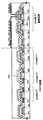
コンタクトホール形成時のポリシリコン膜減り量の理論値を表1に示す。
【0101】
【表1】

表1において、前提条件は、ポリシリコン膜上にゲート絶縁膜(窒素を含む酸化シリコン膜、膜厚120nm±5%)と第1層間絶縁膜(窒素を含む酸化シリコン膜、膜厚200nm±5%)とが積層された状態で、エッチングレートが300nm/minのドライエッチングを行う。エッチングレートは、フッ化水素アンモニウムを7.13%とフッ化アンモニウムを15.4%含む混合溶液(ステラケミファ社製、商品名LAL500)の20℃における値である。縦軸はエッチングレートのばらつきを示し、横軸はポリシリコン膜と窒素を含む酸化シリコン膜の選択比である。
【0103】
例えば、エッチングレートのばらつきが5%であり、オーバーエッチング量が所定値、例えば5nm以下となるようにしたい場合、表1から選択比を10よりも大きく持たせる必要があることが読み取れる。このようにして、表1からオーバーエッチング量を所定値以下とするためには、選択比がどれくらい必要かを求めることができる。また、選択比をある値とした場合、エッチングレートのばらつきはどれくらいに抑える必要があるかを求めることができる。また、第1層間絶縁膜が200nmよりも大きい場合の表を表1と同様に作成した場合、選択比が大きく、エッチングレートのばらつきが極小でないとコンタクトホール形成は困難であることがわかった。
【0104】
本実施例では、ポリシリコンとの選択比が12〜15の絶縁材料を用い、エッチングレートのばらつきを5%以内に抑えたため、オーバーエッチングのほとんどないコンタクトホールを形成することができた。
【0105】
そして、ソース配線151〜154と、ドレイン配線155〜157を形成する。ただし、コンタクトホールの大きさが1μm以下である場合には、コンタクトホールをドライエッチングで形成することが好ましい。なお、CMOS回路を形成するためにドレイン配線155はpチャネル型TFTとnチャネル型TFTとの間で共通化されている。また、図示していないが、本実施例ではこの配線を、Ti膜を200nm、Tiを含むアルミニウム膜500nm、Ti膜100nmをスパッタ法で連続して形成した3層構造の積層膜とする。
【0106】
次に、パッシベーション膜158として、窒化シリコン膜、酸化シリコン膜、または窒化酸化シリコン膜で50〜500nm(代表的には200〜300nm)の厚さで形成する。(図4(C))なお、この状態における上面図を図6(B)及び図7(B)に示す。図6(B)中のA−A’断面が図4(C)A−A’に相当する。また、図7(B)中のB−B’断面が図4(C)B−B’に相当する。
【0107】
この時、本実施例では膜の形成に先立ってH2、NH3等水素を含むガスを用いてプラズマ処理を行い、成膜後に熱処理を行う。この前処理により励起された水素が第1、第2層間絶縁膜中に供給される。この状態で熱処理を行うことで、パッシベーション膜158の膜質を改善するとともに、第1、第2層間絶縁膜中に添加された水素が下層側に拡散するため、効果的に活性層を水素化することができる。
【0108】
また、パッシベーション膜158を形成した後に、さらに水素化工程を行っても良い。例えば、3〜100%の水素を含む雰囲気中で、300〜450℃で1〜12時間の熱処理を行うと良く、あるいはプラズマ水素化法を用いても同様の効果が得られる。なお、水素化工程後に画素電極とドレイン配線を接続するためのコンタクトホールを形成する位置において、パッシベーション膜158に開口部(図示せず)を形成しておいても良い。
【0109】
その後、有機樹脂からなる第3層間絶縁膜159を約1μmの厚さに形成する。有機樹脂としては、ポリイミド、アクリル、ポリアミド、ポリイミドアミド、BCB(ベンゾシクロブテン)等を使用することができる。有機樹脂膜を用いることの利点は、成膜方法が簡単である点や、比誘電率が低いので、寄生容量を低減できる点、平坦性に優れる点などが上げられる。なお上述した以外の有機樹脂膜や有機系SiO化合物などを用いることもできる。ここでは、アクリルを用い、熱焼成して形成する。
【0110】
次に、画素回路となる領域において、第3層間絶縁膜159上に遮蔽膜160を形成する。なお、本明細書中では光と電磁波を遮るという意味で遮蔽膜という文言を用いる。遮蔽膜160はアルミニウム(Al)、チタン(Ti)、タンタル(Ta)から選ばれた元素でなる膜またはいずれかの元素を主成分とする膜で100〜300nmの厚さに形成する。本実施例では1wt%のチタンを含有させたアルミニウム膜を125nmの厚さに形成する。
【0111】
なお、第3層間絶縁膜159上に酸化シリコン膜等の絶縁膜を5〜50nm形成しておくと、この上に形成する遮蔽膜の密着性を高めることができる。また、有機樹脂で形成した第3層間絶縁膜159の表面にCF4ガスを用いたプラズマ処理を施すと、表面改質により膜上に形成する遮蔽膜の密着性を向上させることができる。
【0112】
また、このチタンを含有させたアルミニウム膜を用いて、遮蔽膜だけでなく他の接続配線を形成することも可能である。例えば、駆動回路内で回路間をつなぐ接続配線を形成できる。但し、その場合は遮蔽膜または接続配線を形成する材料を成膜する前に、予め第3層間絶縁膜にコンタクトホールを形成しておく必要がある。
【0113】
次に、遮蔽膜160の表面に陽極酸化法またはプラズマ酸化法(本実施例では陽極酸化法)により20〜100nm(好ましくは30〜50nm)の厚さの酸化物161を形成する。本実施例では遮蔽膜160としてアルミニウムを主成分とする膜を用いたため、陽極酸化物161として酸化アルミニウム膜(アルミナ膜)が形成される。
【0114】
この陽極酸化処理に際して、まず十分にアルカリイオン濃度の小さい酒石酸エチレングリコール溶液を作製する。これは15%の酒石酸アンモニウム水溶液とエチレングリコールとを2:8で混合した溶液であり、これにアンモニア水を加え、pHが7±0.5となるように調節する。そして、この溶液中に陰極となる白金電極を設け、遮蔽膜160が形成されている基板を溶液に浸し、遮蔽膜160を陽極として、一定(数mA〜数十mA)の直流電流を流す。
【0115】
溶液中の陰極と陽極との間の電圧は陽極酸化物の成長に従い時間と共に変化するが、定電流のまま100V/minの昇圧レートで電圧を上昇させて、到達電圧45Vに達したところで陽極酸化処理を終了させる。このようにして遮蔽膜160の表面には厚さ約50nmの陽極酸化物161を形成することができる。また、その結果、遮蔽膜160の膜厚は90nmとなる。なお、ここで示した陽極酸化法に係わる数値は一例にすぎず、作製する素子の大きさ等によって当然最適値は変化しうるものである。
【0116】
また、ここでは陽極酸化法を用いて遮蔽膜表面のみに絶縁膜を設ける構成としたが、絶縁膜をプラズマCVD法、熱CVD法またはスパッタ法などの気相法によって形成しても良い。その場合も膜厚は20〜100nm(好ましくは30〜50nm)とすることが好ましい。また、酸化シリコン膜、窒化シリコン膜、窒化酸化シリコン膜、DLC(Diamond like carbon)膜、酸化タンタル膜または有機樹脂膜を用いても良い。さらに、これらを組み合わせた積層膜を用いても良い。
【0117】
次に、第3層間絶縁膜159、パッシベーション膜158にドレイン配線157に達するコンタクトホールを形成し、画素電極162を形成する。なお、画素電極163は隣接する別の画素の画素電極である。画素電極162、163は、透過型液晶表示装置とする場合には透明導電膜を用い、反射型の液晶表示装置とする場合には金属膜を用いれば良い。ここでは透過型の液晶表示装置とするために、酸化インジウム・スズ(ITO)膜を110nmの厚さにスパッタ法で形成する。
【0118】
また、この時、画素電極162と遮蔽膜160とが陽極酸化物161を介して重なり、保持容量(キャパシタンス・ストレージ)164を形成する。なお、この場合、遮蔽膜160をフローティング状態(電気的に孤立した状態)か固定電位、好ましくはコモン電位(データとして送られる画像信号の中間電位)に設定しておくことが望ましい。
【0119】
こうして同一基板上に、駆動回路と画素回路とを有したアクティブマトリクス基板が完成した。なお、図5においては、駆動回路にはpチャネル型TFT301、nチャネル型TFT302、303が形成され、画素回路にはnチャネル型TFTでなる画素TFT304が形成される。
【0120】
図5の断面図に対応する上面図を図8(B)に示し、共通の符号を用いた。また、図6(B)で示した上面図は図8(A)の一部を示した図であり、共通の符号を用いた。
【0121】
駆動回路のpチャネル型TFT301には、チャネル形成領域201、ソース領域202、ドレイン領域203がそれぞれp型不純物領域(a)で形成される。但し、厳密にはソース202領域及びドレイン領域203に1×10¹⁶〜5×10¹⁸atoms/cm3の濃度でリンを含んでいる。
【0122】
また、nチャネル型TFT302には、チャネル形成領域204、ソース領域205、ドレイン領域206、そしてチャネル形成領域とドレイン領域との間に、ゲート絶縁膜を介してゲート配線と重なった領域(本明細書中ではこのような領域をLov領域という。なお、ovはoverlapの意味で付した。)207が形成される。この時、Lov領域207は2×10¹⁶〜5×10¹⁹atoms/cm3の濃度でリンを含み、且つ、ゲート配線と全部重なるように形成される。
【0123】
また、nチャネル型TFT303には、チャネル形成領域208、ソース領域209、ドレイン領域210、そしてチャネル形成領域を挟むようにしてLDD領域211、212が形成される。即ち、ソース領域とチャネル形成領域との間及びドレイン領域とチャネル形成領域との間にLDD領域が形成される。
【0124】
なお、この構造ではLDD領域211、212の一部がゲート配線と重なるように配置されたために、ゲート絶縁膜を介してゲート配線と重なった領域(Lov領域)とゲート配線と重ならない領域(本明細書中ではこのような領域をLoff領域という。なお、offはoffsetの意味で付した。)が実現されている。
【0125】
また、チャネル長3〜7μmに対してnチャネル型TFT302のLov領域207の長さ(幅)は0.3〜3.0μm、代表的には0.5〜1.5μmとすれば良い。また、nチャネル型TFT303のLov領域の長さ(幅)は0.3〜3.0μm、代表的には0,5〜1.5μm、Loff領域の長さ(幅)は1.0〜3.5μm、代表的には1.5〜2.0μmとすれば良い。また、画素TFT304に設けられるLoff領域217〜220の長さ(幅)は0.5〜3.5μm、代表的には2.0〜2.5μmとすれば良い。
【0126】
また、本実施例ではゲート配線をダブルゲート構造としたが、トリプルゲート構造といったマルチゲート構造として各回路の信頼性を向上させてもよい。また、シングルゲート構造としてもよい。
【0127】
また、本実施例では保持容量の誘電体として比誘電率が7〜9と高いアルミナ膜を用いたことで、必要な容量を形成するために必要な保持容量の占有面積を少なくすることができる。さらに、本実施例のように画素TFT上に形成される遮蔽膜を保持容量の一方の電極とすることで、アクティブマトリクス型液晶表示装置の画像表示部の開口率を向上させることができる。
【0128】
なお、本発明は本実施例に示した保持容量の構造に限定される必要はない。例えば、本出願人による特願平9−316567号出願、特願平9−273444号出願または特願平10−254097号出願に記載された構造の保持容量を用いることもできる。
【0129】
また、本願発明の構造は、ゲート配線と上層配線とが重なった領域に第2の層間絶縁膜を設ける構成に特徴があるので、それ以外の構成については実施者が適宜決定すればよい。
【0130】
ここでアクティブマトリクス基板から、アクティブマトリクス型液晶表示装置を作製する工程を説明する。図9に示すように、図5の状態の基板に対し、配向膜501を形成する。本実施例では配向膜としてポリイミド膜を用いる。また、対向基板502には、透明導電膜503と、配向膜504とを形成する。なお、対向基板には必要に応じてカラーフィルターや遮蔽膜を形成しても良い。
【0131】
次に、配向膜を形成した後、ラビング処理を施して液晶分子がある一定のプレチルト角を持って配向するように調節する。そして、画素回路と、駆動回路が形成されたアクティブマトリクス基板と対向基板とを、公知のセル組み工程によってシール材507やスペーサ506などを介して貼りあわせる。その後、両基板の間に液晶505を注入し、封止剤(図示せず)によって完全に封止する。液晶には公知の液晶材料を用いれば良い。このようにして図9に示すアクティブマトリクス型液晶表示装置が完成する。
【0132】
次に、このアクティブマトリクス型液晶表示装置の構成を、図10の斜視図を用いて説明する。なお、図10は、図1〜図5の断面構造図と対応付けるため、共通の符号を用いている。アクティブマトリクス基板は、石英基板101上に形成された、画素回路801と、ゲート線(走査線)側駆動回路802と、ソース線(信号線)側駆動回路803で構成される。画素回路の画素TFT304はnチャネル型TFTであり、周辺に設けられる駆動回路はCMOS回路を基本として構成されている。ゲート線側駆動回路802と、ソース線側駆動回路803はそれぞれゲート配線128とソース配線154で画素回路801に接続されている。また、FPC804が接続された外部入出力端子805から駆動回路の入出力端子までの接続配線806、807が設けられている。
【0133】
次に、図10に示したアクティブマトリクス型液晶表示装置の回路構成の一例を図11に示す。本実施例のアクティブマトリクス型液晶表示装置は、画像信号駆動回路901、ゲート線側駆動回路(A)907、ゲート線側駆動回路(B)911、プリチャージ回路912、画素回路906を有している。なお、本明細書中において、駆動回路にはソース線側駆動回路901およびゲート線側駆動回路907が含まれる。
【0134】
ソース線側駆動回路901は、シフトレジスタ回路902、レベルシフタ回路903、バッファ回路904、サンプリング回路905を備えている。また、ゲート線側駆動回路(A)907は、シフトレジスタ回路908、レベルシフタ回路909、バッファ回路910を備えている。ゲート線側駆動回路(B)911も同様な構成である。
【0135】
このように本発明は、同一基板上に画素回路と該画素回路を制御するための駆動回路とを少なくとも含む半導体装置、例えば同一基板上に信号処理回路、駆動回路および画素回路とを具備した半導体装置を実現しうる。
【0136】
また、本実施例の図2(A)までの工程を行うと、結晶格子に連続性を持つ特異な結晶構造の結晶質シリコン膜が形成される。以下、本出願人が実験的に調べた結晶構造の特徴について概略を説明する。なお、この特徴は、本実施例によって完成されたTFTの活性層を形成する半導体層の特徴と一致する。
【0137】
上記結晶質シリコン膜は、微視的に見れば複数の針状又は棒状の結晶(以下、棒状結晶と略記する)が集まって並んだ結晶構造を有する。このことはTEM(透過型電子顕微鏡法)による観察で容易に確認できる。
【0138】
また、電子線回折及びエックス線(X線)回折を利用すると結晶質シリコン膜の表面(チャネルを形成する部分)が、結晶軸に多少のずれが含まれているものの主たる配向面として{110}面を有することを確認できる。この時、電子線回折で分析を行えば{110}面に対応する回折斑点がきれいに現れるのを確認することができる。また、各斑点は同心円上に分布を持っていることも確認できる。
【0139】
また、個々の棒状結晶が接して形成する結晶粒界をHR−TEM(高分解能透過型電子顕微鏡法)により観察すると、結晶粒界において結晶格子に連続性があることを確認できる。これは観察される格子縞が結晶粒界において連続的に繋がっていることから容易に確認することができる。
【0140】
なお、結晶粒界における結晶格子の連続性は、その結晶粒界が「平面状粒界」と呼ばれる粒界であることに起因する。本明細書における平面状粒界の定義は、「Characterization of High-Efficiency Cast-Si Solar Cell Wafers by MBIC Measurement ;Ryuichi Shimokawa and Yutaka Hayashi,Japanese Journal of Applied Physics vol.27,No.5,pp.751-758,1988」に記載された「Planar boundary 」である。
【0141】
上記論文によれば、平面状粒界には双晶粒界、特殊な積層欠陥、特殊なtwist 粒界などが含まれる。この平面状粒界は電気的に不活性であるという特徴を持つ。即ち、結晶粒界でありながらキャリアの移動を阻害するトラップとして機能しないため、実質的に存在しないと見なすことができる。
【0142】
特に結晶軸(結晶面に垂直な軸)が〈110〉軸である場合、{211}双晶粒界はΣ3の対応粒界とも呼ばれる。Σ値は対応粒界の整合性の程度を示す指針となるパラメータであり、Σ値が小さいほど整合性の良い粒界であることが知られている。
【0143】
実際に本実施例の結晶質シリコン膜を詳細にTEMを用いて観察すれば、結晶粒界の殆ど(90%以上、典型的には95%以上)がΣ3の対応粒界、典型的には{211}双晶粒界であることが判る。
【0144】
二つの結晶粒の間に形成された結晶粒界において、両方の結晶の面方位が{110}である場合、{111}面に対応する格子縞がなす角をθとすると、θ=70.5°の時にΣ3の対応粒界となることが知られている。本実施例の結晶質シリコン膜は、結晶粒界において隣接する結晶粒の各格子縞がまさに約70.5°の角度で連続しており、その事からこの結晶粒界はΣ3の対応粒界であると言える。
【0145】
なお、θ= 38.9 °の時にはΣ9の対応粒界となるが、この様な他の対応粒界も存在する。いずれにしても不活性であることに変わりはない。
【0146】
この様な対応粒界は、同一面方位の結晶粒の間にしか形成されない。即ち、本実施例の結晶質シリコン膜は面方位が概略{110}で揃っているからこそ、広範囲に渡ってこの様な対応粒界を形成しうる。
【0147】
この様な結晶構造(正確には結晶粒界の構造)は、結晶粒界において異なる二つの結晶粒が極めて整合性よく接合していることを示している。即ち、結晶粒界において結晶格子が連続的に連なり、結晶欠陥等に起因するトラップ準位を非常に作りにくい構成となっている。従って、この様な結晶構造を有する半導体薄膜は実質的に結晶粒界が存在しない見なすことができる。
【0148】
またさらに、800〜1150℃という高い温度での熱処理工程(実施例1における熱酸化工程に相当する)によって結晶粒内に存在する欠陥が殆ど消滅していることがTEM観察によって確認されている。これはこの熱処理工程の前後で欠陥数が大幅に低減されていることからも明らかである。
【0149】
この欠陥数の差は電子スピン共鳴分析(Electron Spin Resonance :ESR)によってスピン密度の差となって現れる。現状では本実施例の結晶質シリコン膜のスピン密度は少なくとも 5×10¹⁷spins/cm3以下(好ましくは 3×10¹⁷spins/cm3以下)であることが判明している。ただし、この測定値は現存する測定装置の検出限界に近いので、実際のスピン密度はさらに低いと予想される。
【0150】
以上の事から、本実施例の結晶質シリコン膜は結晶粒内の欠陥が極端に少なく、結晶粒界が実質的に存在しないと見なせるため、単結晶シリコン膜又は実質的な単結晶シリコン膜と考えて良い。
【0151】
[実施例2]
実施例1では、結晶構造を含む半導体膜の形成方法として、結晶化を助長する触媒元素を用いる例を示したが、本実施例では、そのような触媒元素を用いずに熱結晶化またはレーザー結晶化によって結晶構造を含む半導体膜を形成する場合を示す。
【0152】
熱結晶化による場合、非晶質構造を示す半導体膜を形成した後、600〜650℃の温度で15〜24時間の熱処理を行えばよい。即ち、600℃を越える温度で熱処理を行うことにより自然核が発生し、結晶化が進行する。
【0153】
また、レーザー結晶化による場合、非晶質構造を含む半導体膜を形成した後、レーザーアニ―ルを行えばよい。これにより短時間で結晶構造を含む半導体膜を形成することができる。勿論、レーザーアニ―ルの代わりにランプアニ―ルを用いてもよい。また、基板として、石英基板の他にガラス基板やプラスチック基板を用いることが可能である。
【0154】
また、基板上に下地膜と非晶質シリコン膜とを大気解放しないで連続的に形成することも有効である。そうすることにより基板表面の汚染が非晶質シリコン膜に影響を与えないようにすることが可能となり、作製されるTFTの特性バラツキを低減させることができる。
【0155】
このように、本発明に用いる結晶構造を含む半導体膜は、公知のあらゆる手段を用いて形成することができる。
【0156】
[実施例3]
本実施例は、実施例1とは異なる方法によりコンタクトホールを形成する例である。本実施例では、活性化の後、コンタクトホールを形成し、第2層間絶縁膜を積層した後、再度パターニングを行うことによってコンタクトホールを形成する。基本的な構成は、実施例1とほぼ同様であるので、相違点のみに着目して説明する。
【0157】
まず、実施例1に従って、第1の層間絶縁膜149を積層した後、活性化を行い、図3(D)の状態を得る。なお、図3(D)に対応する図を図12(A)に示す。
【0158】
次いで、ソース領域またはドレイン領域に達するコンタクトホールを形成する。なお、同一のマスクを用いてゲート絶縁膜と第1層間絶縁膜とを同時または順次エッチングする。(図12(B))この時のエッチングをドライエッチングで行えば微細なコンタクトホール(0.5μm〜1.5μm)の形成が可能である。
【0159】
次いで、第2層間絶縁膜1201を積層し、図12(C)の状態を得る。第2層間絶縁膜は実施例1と同一の組成を有する絶縁膜を用いた。次いで、第2層間絶縁膜1201のパターニングを行った後、実施例1と同様にソース配線、ドレイン配線の形成を行い、実施例1の図4(C)に相当する図12(D)の状態を得る。なお、第2層間絶縁膜のパターニングにおいて、ウエットエッチングを用いるとテーパー形状が得られるので、その上に形成されるソース配線、ドレイン配線のカバレッジが良好となる。以降の工程は実施例1と同一であるため省略する。
【0160】
このように、本実施例では、膜質の異なる第1層間絶縁膜と第2層間絶縁膜とを別々にエッチングすることで、オーバーエッチングが少なく、形状の良好なコンタクトホールを形成することができる。こうすることにより、確実なコンタクト接続が行えるため歩留まりを向上させることができた。
【0161】
なお、本実施例の構成は実施例1または実施例2の構成と自由に組み合わせることが可能である。
【0162】
[実施例4]
本実施例は、ゲート絶縁膜のパターニングをゲート電極のパターニング後に行い、コンタクトホール形成を容易に可能とした例である。基本的な構成は、実施例1とほぼ同様であるので、相違点のみに着目して説明する。
【0163】
まず、実施例1に従って、図2(E)の状態を得る。なお、図2(E)に対応する図を図13(A)に示す。
【0164】
次いで、ゲート電極をマスクとしてエッチングを行いゲート絶縁膜1301を形成した。(図13(B))その後、レジストマスク1304を用いてp型不純物元素のドーピングを行い、実施例1と同じ濃度に添加されたp型不純物領域(a)1302、1303を形成する。ただし、活性層が露呈した状態でドーピングを行うため実施例1とはドーピング条件を変えなければならない。(図13(C))
【0165】
次にレジストマスク1304を除去し、レジストマスク1305〜1308を形成する。そして、レジストマスク1305〜1308を用いてn型不純物元素のドーピングを行い、実施例1と同じ濃度に添加されたn型不純物領域(a)1309〜1315を形成する。ただし、実施者は活性層が露呈した状態でドーピングを行うため実施例1とはドーピング条件を変えなければならない。(図13(D))
【0166】
次にレジストマスク1305〜1308を除去し、ゲート電極をマスクとしてn型不純物元素のドーピングを行い、実施例1と同じ濃度に添加されたn型不純物領域(c)1401〜1404を形成する。ただし、実施者は活性層が露呈した状態でドーピングを行うため実施例1とはドーピング条件を変えなければならない。(図14(A))
【0167】
次いで、実施例1と同様にして第1層間絶縁膜1405の成膜を行った後、活性化工程を行った。(図14(B))ただし、本実施例においては、第1層間絶縁膜のみで活性層が覆われている部分があるため、活性層を保護する最低限の膜厚が第1層間絶縁膜に必要とされる。ここでの第1層間絶縁膜の膜厚として、代表的には50nm〜200nmであればよい。
【0168】
次いで、実施例1と同様に第2層間絶縁膜1406を形成する。(図14(C))
【0169】
次いで、実施例1と同様に第1層間絶縁膜と第2層間絶縁膜を同時または順次エッチングを行ってソース領域またはドレイン領域に達するコンタクトホールを形成した後、ソース配線及びドレイン配線を形成する。(図14(D))以降の工程は実施例1と同一であるため省略する。
【0170】
また、本実施例においては、ゲート絶縁膜のエッチングをゲート配線形成直後に行った例を示したが、ゲート絶縁膜の除去工程を施すのは、ゲート配線形成直後から第2層間絶縁膜形成前までの間であればよい。
【0171】
こうすることにより、開口する絶縁膜の積層数を低減できるので歩留まりを向上させることができた。ただし、実施例1と同様に第1層間絶縁膜と第2層間絶縁膜のエッチングレートを考慮にいれることが必要である。
【0172】
なお、本実施例の構成は実施例1〜3の構成を自由に組み合わせることが可能である。
【0173】
[実施例5]
本実施例では、本発明をシリコン基板上に作製した半導体装置に適用した場合について説明する。典型的には、画素電極として反射率の高い金属膜を用いた反射型液晶表示装置に適用できる。
【0174】
本実施例は、実施例1の基板としてシリコン基板(シリコンウェハ)を用い、シリコン基板に直接的にn型またはp型不純物元素を添加してLDD領域、ソース領域またはドレイン領域といった不純物領域を形成する。その際、各不純物領域の形成順序やゲート絶縁膜の形成順序は問わない。
【0175】
なお、本実施例の構成は実施例1〜4のいずれの構成とも自由に組み合わせることが可能である。但し、活性層となる半導体層は単結晶シリコン基板と決まっているので、結晶化工程以外での組み合わせとなる。
【0176】
[実施例6]
本発明は従来のMOSFET上に層間絶縁膜を形成し、その上にTFTを形成する際に用いることも可能である。即ち、三次元構造の半導体装置を実現することも可能である。また、基板としてSIMOX、Smart−Cut(SOITEC社の登録商標)、ELTRAN(キャノン株式会社の登録商標)などのSOI基板を用いることも可能である。
【0177】
なお、本実施例の構成は、実施例1〜5のいずれの構成とも自由に組み合わせることが可能である。
【0178】
[実施例7]
本実施例では、同一基板上にメモリ部と駆動回路とを一体形成した半導体装置に適用した場合について説明する。
【0179】
なお、メモリ部は不揮発性メモリ(ここではEEPROM)で形成され、図15ではそのメモリセルに形成される一つのメモリトランジスタ(メモリセルトランジスタともいう)を例示する。実際には複数のメモリセルが集積化されてメモリ部を形成する。ここでは集積度の高いフラッシュメモリ(フラッシュEEPROM)を用いて説明する。
【0180】
メモリトランジスタはソース領域1505、ドレイン領域1508、低濃度不純物領域(LDD領域ともいう)1506及びチャネル形成領域1507を含む活性層、ゲート絶縁膜1500、第1層間絶縁膜1501、第2層間絶縁膜1502c、浮遊ゲート電極1509、第3ゲート絶縁膜11、制御ゲート電極1510、そして第3層間絶縁膜1503を介して形成された共通ソース配線1512、ビット配線(ドレイン配線)1511を有して形成される。
【0181】
ソース領域1505は浮遊ゲート電極1509に捕獲されたキャリア(電子)を共通ソース配線1512に引き抜くための領域であり消去領域とも言える。なお、図15ではチャネル形成領域1507との間にLDD領域1506を設けているが、形成しなくても良い。また、ドレイン領域1508は電気的に孤立した浮遊ゲート電極1509にキャリアを注入するための領域であり書き込み領域とも言える。さらに、ドレイン領域1508はメモリトランジスタに記憶されたデータをビット配線1511に読み出すための読み出し領域としても機能する。
【0182】
なお、ゲート絶縁膜1500としてはトンネル電流(ファウラノルドハイム電流)が流れる程度に薄い絶縁膜(膜厚が3〜20nm、好ましくは5〜10nm)を用いる必要があるため、活性層を酸化して得られた酸化膜(活性層が珪素ならば酸化珪素膜)を用いることが好ましい。勿論、膜厚の均一性と確執さえ良ければ、CVD法やスパッタ法等の気相法で第1ゲート絶縁膜を形成することもできる。
【0183】
本実施例においては、制御ゲート電極1510とビット配線1511または共通ソース配線1512との重なり部分に生じる寄生容量を第2層間絶縁膜1502cによって低減した。
【0184】
また、駆動回路部を形成する具体例としてCMOS回路を示す。実際には、CMOS回路を基本回路としてフリップフロップ回路等の論理回路が形成され、それらが集積化されて駆動回路部を形成する。CMOS回路においても、ゲート配線と上層配線との寄生容量を低減するための第2層間絶縁膜1502a、1502bが設けられている。
【0185】
このように本願発明は様々な半導体素子に適用することができる。
【0186】
なお、本実施例の構成は、実施例1〜6のいずれの構成とも自由に組み合わせることが可能である。
【0187】
[実施例8]
本実施例では異方性エッチングを利用した例である。基本的な構成は、実施例1または実施例3とほぼ同様であるので、相違点のみに着目して図16を用いて説明する。
【0188】
本実施例においては、実施例3と同様にゲート電極をマスクとして、ゲート絶縁膜をエッチングし、第1層間絶縁膜を成膜した後、活性化を行って図14(B)と同じ状態を得た。
【0189】
次いで、第1層間絶縁膜に異方性エッチングを行い、ゲート電極の両側に三角形状の絶縁物1601を形成する。この際、ゲート配線を保護するための保護膜(図示しない)をあらかじめ形成しておくことが好ましい。
【0190】
次いで、第2の層間絶縁膜1602を形成する。その後、第2層間絶縁膜にエッチングを行ってソース領域またはドレイン領域に達するコンタクトホールを形成した後、ソース配線及びドレイン配線を形成する。以降の工程は実施例1と同一であるため省略する。
【0191】
こうすることにより、開口する絶縁膜の積層数を低減できるのでコンタクトホール形成が簡略化され、歩留まりを向上させることができた。
【0192】
また、ゲート電極形成直後に三角形状の絶縁物1601を形成し、それを利用してLDD領域などの不純物領域を形成する工程としてもよい。
【0193】
なお、本実施例の構成は、実施例1〜7のいずれの構成とも自由に組み合わせることが可能である。
【0194】
[実施例9]
本実施例では、本発明をボトムゲート型TFTに用いた場合について説明する。具体的には、逆スタガ型TFTに用いた場合を図17に示す。本発明の逆スタガ型TFTの場合、実施例1のトップゲート型TFTとはゲート配線と活性層の位置関係が異なる以外、特に大きく異なることはない。従って、本実施例では、図5に示した構造と大きく異なる点に注目して説明を行い、その他の部分は図5と同一であるため説明を省略する。実施例1と同様にして、寄生容量を低減するための第2層間絶縁膜46、47が形成されている。この第2層間絶縁膜は実施例1に示した方法で形成する。
【0195】
図17において、11、12はそれぞれシフトレジスタ回路等を形成するCMOS回路のpチャネル型TFT、nチャネル型TFT、13はサンプリング回路等を形成するnチャネル型TFT、14は画素回路を形成するnチャネル型TFTである。これらは下地膜を設けた基板上に形成されている。
【0196】
また、15はpチャネル型TFT11のゲート配線、16はnチャネル型TFT12のゲート配線、17はnチャネル型TFT13のゲート配線、18はnチャネル型TFT14のゲート配線であり、実施例1で説明したゲート配線と同じ材料を用いて形成することができる。また、19はゲート絶縁膜であり、これも実施例1と同じ材料を用いることができる。
【0197】
その上には各TFT11〜14の活性層(活性層)が形成される。なお、ゲート絶縁膜及び活性層を構成する半導体膜の作製時においては、大気にふれることなくスパッタ法またはPCVD法で連続成膜を行い、形成することが好ましい。pチャネル型TFT11の活性層には、ソース領域20、ドレイン領域21、チャネル形成領域22が形成される。
【0198】
また、nチャネル型TFT12の活性層には、ソース領域23、ドレイン領域24、LDD領域(この場合、Lov領域25)、チャネル形成領域26が形成される。
【0199】
また、nチャネル型TFT13の活性層には、ソース領域27、ドレイン領域28、LDD領域(この場合、Lov領域29a、30a及びLoff領域29b、30b)、チャネル形成領域31が形成される。
【0200】
また、nチャネル型TFT14の活性層には、ソース領域32、ドレイン領域33、LDD領域(この場合、Loff領域34〜37)、チャネル形成領域38、39、n+領域40が形成される。
【0201】
なお、41〜45で示される絶縁膜は、チャネル形成領域を保護する目的とLDD領域を形成する目的のために形成されている。
【0202】
以上のように本発明を逆スタガ型TFTに代表されるボトムゲート型TFTに適用することは容易である。なお、本実施例の逆スタガ型TFTを作製するにあたっては、本明細書中に記載された他の実施例に示される作製工程を、公知の逆スタガ型TFTの作製工程に適用すれば良い。
【0203】
なお、本実施例の構成は、実施例1〜8のいずれの構成とも自由に組み合わせることが可能である。
【0204】
[実施例10]
本発明はアクティブマトリクス型EL(エレクトロルミネッセンス)ディスプレイに適用することも可能である。その例を図18に示す。
【0205】
図18はアクティブマトリクス型ELディスプレイの回路図である。81は画素回路を表しており、その周辺にはX方向駆動回路82、Y方向駆動回路83が設けられている。また、画素回路81の各画素は、スイッチ用TFT84、コンデンサ85、電流制御用TFT86、有機EL素子87を有し、スイッチ用TFT84にX方向信号線88a(または88b)、Y方向信号線89a(または89b、89c)が接続される。また、電流制御用TFT86には、電源線90a、90bが接続される。
【0206】
本実施例のアクティブマトリクス型ELディスプレイでは、X方向駆動回路82、Y方向駆動回路83または電流制御用TFT86に用いられるTFTを5のpチャネル型TFT301、nチャネル型TFT302または303を組み合わせて形成する。また、スイッチ用TFT84のTFTを図5のnチャネル型TFT304で形成する。
【0207】
なお、本実施例のアクティブマトリクス型ELディスプレイに対して、実施例1〜9のいずれの構成を組み合わせても良い。
【0208】
[実施例11]
本発明によって作製された液晶表示装置は様々な液晶材料を用いることが可能である。そのような材料として、TN液晶、PDLC(ポリマー分散型液晶)、FLC(強誘電性液晶)、AFLC(反強誘性電液晶)、またはFLCとAFLCの混合物が挙げられる。
【0209】
例えば、「H.Furue et al.;Charakteristics and Drivng Scheme of Polymer-Stabilized Monostable FLCD Exhibiting Fast Response Time and High Contrast Ratio with Gray-Scale Capability,SID,1998」、「T.Yoshida et al.;A Full-Color Thresholdless Antiferroelectric LCD Exhibiting Wide Viewing Angle with Fast Response Time,841,SID97DIGEST,1997」、または米国特許第5,594,569号に開示された材料を用いることができる。
【0210】
特に、しきい値なし(無しきい値)の反強誘電性液晶(Thresholdless Antiferroelectric LCD:TL−AFLCと略記する)を使うと、液晶の動作電圧を±2.5V程度に低減しうるため電源電圧として5〜8V程度で済む場合がある。即ち、ドライバー回路と画素マトリクス回路を同じ電源電圧で動作させることが可能となり、液晶表示装置全体の低消費電力化を図ることができる。
【0211】
また、無しきい値反強誘電性液晶は、V字型の電気光学応答特性を示すものがあり、その駆動電圧が約±2.5V程度(セル厚約1μm〜2μm)のものも見出されている。
【0212】
ここで、V字型の電気光学応答を示す無しきい値反強誘電性混合液晶の印加電圧に対する光透過率の特性を示す例を図19に示す。図19に示すグラフの縦軸は透過率(任意単位)、横軸は印加電圧である。なお、液晶パネルの入射側の偏光板の透過軸は、液晶パネルのラビング方向にほぼ一致する無しきい値反強誘電性混合液晶のスメクティック層の法線方向とほぼ平行に設定されている。また、出射側の偏光板の透過軸は、入射側の偏光板の透過軸に対してほぼ直角(クロスニコル)に設定されている。
【0213】
また、強誘電性液晶や反強誘電性液晶はTN液晶に比べて応答速度が速いという利点をもつ。上記実施例で用いるような結晶質TFTは非常に動作速度の速いTFTを実現しうるため、強誘電性液晶や反強誘電性液晶の応答速度の速さを十分に生かした画像応答速度の速い液晶表示装置を実現することが可能である。
【0214】
なお、本実施例の液晶表示装置をパーソナルコンピュータ等の電子機器の表示ディスプレイとして用いることが有効であることは言うまでもない。
【0215】
また、本実施例の構成は、実施例1〜9のいずれの構成とも自由に組み合わせることが可能である。
【0216】
[実施例12]
本実施例では、本発明を用いてEL(エレクトロルミネセンス)表示装置を作製した例について説明する。なお、図20(A)は本発明のEL表示装置の上面図であり、図20(B)はその断面図である。
【0217】
図20(A)において、4001は基板、4002は画素部、4003はソース側駆動回路、4004はゲート側駆動回路であり、それぞれの駆動回路は配線4005を経てFPC(フレキシブルプリントサーキット)4006に至り、外部機器へと接続される。
【0218】
このとき、画素部4002、ソース側駆動回路4003及びゲート側駆動回路4004を囲むようにして第1シール材4101、カバー材4102、充填材4103及び第2シール材4104が設けられている。
【0219】
また、図20(B)は図20(A)をA−A’で切断した断面図に相当し、基板4001の上にソース側駆動回路4003に含まれる駆動TFT(但し、ここではnチャネル型TFTとpチャネル型TFTを図示している。)4201及び画素部4002に含まれる電流制御用TFT(EL素子への電流を制御するTFT)4202が形成されている。
【0220】
本実施例では、駆動TFT4201には図5のpチャネル型TFTまたはnチャネル型TFTと同じ構造のTFTが用いられ、電流制御用TFT4202には図5のpチャネル型TFTと同じ構造のTFTが用いられる。また、画素部4002には電流制御用TFT4202のゲートに接続された保持容量(図示せず)が設けられる。
【0221】
駆動TFT4201及び画素TFT4202の上には樹脂材料でなる層間絶縁膜(平坦化膜)4301が形成され、その上に画素TFT4202のドレインと電気的に接続する画素電極(陽極)4302が形成される。画素電極4302としては仕事関数の大きい透明導電膜が用いられる。透明導電膜としては、酸化インジウムと酸化スズとの化合物、酸化インジウムと酸化亜鉛との化合物、酸化亜鉛、酸化スズまたは酸化インジウムを用いることができる。また、前記透明導電膜にガリウムを添加したものを用いても良い。
【0222】
そして、画素電極4302の上には絶縁膜4303が形成され、絶縁膜4303は画素電極4302の上に開口部が形成されている。この開口部において、画素電極4302の上にはEL(エレクトロルミネッセンス)層4304が形成される。EL層4304は公知の有機EL材料または無機EL材料を用いることができる。また、有機EL材料には低分子系(モノマー系)材料と高分子系(ポリマー系)材料があるがどちらを用いても良い。
【0223】
EL層4304の形成方法は公知の蒸着技術もしくは塗布法技術を用いれば良い。また、EL層の構造は正孔注入層、正孔輸送層、発光層、電子輸送層または電子注入層を自由に組み合わせて積層構造または単層構造とすれば良い。
【0224】
EL層4304の上には周期表の1族または2族に属する元素を含む導電膜(代表的にはアルミニウム、銅もしくは銀に、アルカリ金属元素もしくはアルカリ土類金属元素を含ませた導電膜)からなる陰極4305が形成される。また、陰極4305とEL層4304の界面に存在する水分や酸素は極力排除しておくことが望ましい。従って、真空中で両者を連続成膜するか、EL層4304を窒素または希ガス雰囲気で形成し、酸素や水分に触れさせないまま陰極4305を形成するといった工夫が必要である。本実施例ではマルチチャンバー方式(クラスターツール方式)の成膜装置を用いることで上述のような成膜を可能とする。
【0225】
そして陰極4305は4306で示される領域において配線4005に電気的に接続される。配線4005は陰極4305に所定の電圧を与えるための配線であり、異方導電性フィルム4307を介してFPC4006に電気的に接続される。
【0226】
以上のようにして、画素電極(陽極)4302、EL層4304及び陰極4305からなるEL素子が形成される。このEL素子は、第1シール材4101及び第1シール材4101によって基板4001に貼り合わされたカバー材4102で囲まれ、充填材4103により封入されている。
【0227】
カバー材4102としては、ガラス材、金属材(代表的にはステンレス材)、セラミックス材、プラスチック材(プラスチックフィルムも含む)を用いることができる。プラスチック材としては、FRP(Fiberglass−Reinforced Plastics)板、PVF(ポリビニルフルオライド)フィルム、マイラーフィルム、ポリエステルフィルムまたはアクリル樹脂フィルムを用いることができる。また、アルミニウムホイルをPVFフィルムやマイラーフィルムで挟んだ構造のシートを用いることもできる。
【0228】
但し、EL素子からの光の放射方向がカバー材側に向かう場合にはカバー材は透明でなければならない。その場合には、ガラス板、プラスチック板、ポリエステルフィルムまたはアクリルフィルムのような透明物質を用いる。
【0229】
また、充填材4103としては紫外線硬化樹脂または熱硬化樹脂を用いることができ、PVC(ポリビニルクロライド)、アクリル、ポリイミド、エポキシ樹脂、シリコーン樹脂、PVB(ポリビニルブチラル)またはEVA(エチレンビニルアセテート)を用いることができる。この充填材4103の内部に吸湿性物質(好ましくは酸化バリウム)もしくは酸素を吸着しうる物質を設けておくとEL素子の劣化を抑制できる。
【0230】
また、充填材4103の中にスペーサを含有させてもよい。このとき、スペーサを酸化バリウムで形成すればスペーサ自体に吸湿性をもたせることが可能である。また、スペーサを設けた場合、スペーサからの圧力を緩和するバッファ層として陰極4305上に樹脂膜を設けることも有効である。
【0231】
また、配線4005は異方導電性フィルム4307を介してFPC4006に電気的に接続される。配線4005は画素部4002、ソース側駆動回路4003及びゲート側駆動回路4004に送られる信号をFPC4006に伝え、FPC4006により外部機器と電気的に接続される。
【0232】
また、本実施例では第1シール材4101の露呈部及びFPC4006の一部を覆うように第2シール材4104を設け、EL素子を徹底的に外気から遮断する構造となっている。こうして図20(B)の断面構造を有するEL表示装置となる。
【0233】
ここで画素部のさらに詳細な断面構造を図21に、上面構造を図22(A)に、回路図を図22(B)に示す。図21、図22(A)及び図22(B)では共通の符号を用いるので互いに参照すれば良い。
【0234】
図21において、基板4401上に設けられたスイッチング用TFT4402は図5のnチャネル型TFTを用いて形成される。従って、構造の説明はnチャネル型TFTの説明を参照すれば良い。また、4403で示される配線は、スイッチング用TFT4402のゲート電極4404a、4404bを電気的に接続するゲート配線である。
【0235】
なお、本実施例ではチャネル形成領域が二つ形成されるダブルゲート構造としているが、チャネル形成領域が一つ形成されるシングルゲート構造もしくは三つ形成されるトリプルゲート構造であっても良い。
【0236】
また、スイッチング用TFT4402のドレイン配線4405は電流制御用TFT4406のゲート電極4407に電気的に接続されている。なお、電流制御用TFT4406は図5のpチャネル型TFT301を用いて形成される。従って、構造の説明はpチャネル型TFT301の説明を参照すれば良い。なお、本実施例ではシングルゲート構造としているが、ダブルゲート構造もしくはトリプルゲート構造であっても良い。
【0237】
スイッチング用TFT4402及び電流制御用TFT4406の上には第1パッシベーション膜4408が設けられ、その上に樹脂からなる平坦化膜4409が形成される。平坦化膜4409を用いてTFTによる段差を平坦化することは非常に重要である。後に形成されるEL層は非常に薄いため、段差が存在することによって発光不良を起こす場合がある。従って、EL層をできるだけ平坦面に形成しうるように画素電極を形成する前に平坦化しておくことが望ましい。
【0238】
また、4410は透明導電膜からなる画素電極(EL素子の陽極)であり、電流制御用TFT4406のドレイン配線4411に電気的に接続される。透明導電膜としては、酸化インジウムと酸化スズとの化合物、酸化インジウムと酸化亜鉛との化合物、酸化亜鉛、酸化スズまたは酸化インジウムを用いることができる。また、前記透明導電膜にガリウムを添加したものを用いても良い。
【0239】
画素電極4410の上にはEL層4411が形成される。なお、図21では一画素しか図示していないが、本実施例ではR(赤)、G(緑)、B(青)の各色に対応したEL層を作り分けている。また、本実施例では蒸着法により低分子系有機EL材料を形成している。具体的には、正孔注入層として20nm厚の銅フタロシアニン(CuPc)膜を設け、その上に発光層として70nm厚のトリス−8−キノリノラトアルミニウム錯体(Alq3)膜を設けた積層構造としている。Alq3にキナクリドン、ペリレンもしくはDCM1といった蛍光色素を添加することで発光色を制御することができる。
【0240】
但し、以上の例はEL層として用いることのできる有機EL材料の一例であって、これに限定する必要はまったくない。発光層、電荷輸送層または電荷注入層を自由に組み合わせてEL層(発光及びそのためのキャリアの移動を行わせるための層)を形成すれば良い。例えば、本実施例では低分子系有機EL材料をEL層として用いる例を示したが、高分子系有機EL材料を用いても良い。また、電荷輸送層や電荷注入層として炭化珪素等の無機材料を用いることも可能である。これらの有機EL材料や無機材料は公知の材料を用いることができる。
【0241】
次に、EL層4411の上には導電膜からなる陰極4412が設けられる。本実施例の場合、導電膜としてアルミニウムとリチウムとの合金膜を用いる。勿論、公知のMgAg膜(マグネシウムと銀との合金膜)を用いても良い。陰極材料としては、周期表の1族もしくは2族に属する元素からなる導電膜もしくはそれらの元素を添加した導電膜を用いれば良い。
【0242】
この陰極4412まで形成された時点でEL素子4413が完成する。なお、ここでいうEL素子4413は、画素電極(陽極)4410、EL層4411及び陰極4412で形成されたコンデンサを指す。
【0243】
次に、本実施例における画素の上面構造を図22(A)を用いて説明する。スイッチング用TFT4402のソースはソース配線4415に接続され、ドレインはドレイン配線4405に接続される。また、ドレイン配線4405は電流制御用TFT4406のゲート電極4407に電気的に接続される。また、電流制御用TFT4406のソースは電流供給線4416に電気的に接続され、ドレインはドレイン配線4417に電気的に接続される。また、ドレイン配線4417は点線で示される画素電極(陽極)4418に電気的に接続される。
【0244】
このとき、4419で示される領域には保持容量が形成される。保持容量4419は、電流供給線4416と電気的に接続された半導体膜4420、ゲート絶縁膜と同一層の絶縁膜(図示せず)及びゲート電極4407との間で形成される。また、ゲート電極4407、第1層間絶縁膜と同一の層(図示せず)及び電流供給線4416で形成される容量も保持容量として用いることが可能である。
【0245】
〔実施例13〕
本実施例では、実施例12とは異なる画素構造を有したEL表示装置について説明する。説明には図23を用いる。なお、図22と同一の符号が付してある部分については実施例12の説明を参照すれば良い。
【0246】
図23では電流制御用TFT4501として図5のnチャネル型TFTと同一構造のTFTを用いる。勿論、電流制御用TFT4501のゲート電極4502はスイッチング用TFT4402のドレイン配線4405に電気的に接続されている。また、電流制御用TFT4501のドレイン配線4503は画素電極4504に電気的に接続されている。
【0247】
本実施例では、導電膜からなる画素電極4504がEL素子の陰極として機能する。具体的には、アルミニウムとリチウムとの合金膜を用いるが、周期表の1族もしくは2族に属する元素からなる導電膜もしくはそれらの元素を添加した導電膜を用いれば良い。
【0248】
画素電極4504の上にはEL層4505が形成される。なお、図23では一画素しか図示していないが、本実施例ではG(緑)に対応したEL層を蒸着法及び塗布法(好ましくはスピンコーティング法)により形成している。具体的には、電子注入層として20nm厚のフッ化リチウム(LiF)膜を設け、その上に発光層として70nm厚のPPV(ポリパラフェニレンビニレン)膜を設けた積層構造としている。
【0249】
次に、EL層4505の上には透明導電膜からなる陽極4506が設けられる。本実施例の場合、透明導電膜として酸化インジウムと酸化スズとの化合物もしくは酸化インジウムと酸化亜鉛との化合物からなる導電膜を用いる。
【0250】
この陽極4506まで形成された時点でEL素子4507が完成する。なお、ここでいうEL素子4507は、画素電極(陰極)4504、EL層4505及び陽極4506で形成されたコンデンサを指す。
【0251】
EL素子に加える電圧が10V以上といった高電圧の場合には、電流制御用TFT4501においてホットキャリア効果による劣化が顕在化してくる。このような場合に、電流制御用TFT4501として本発明の構造のnチャネル型TFTを用いることは有効である。
【0252】
また、本実施例の電流制御用TFT4501はゲート電極4502とLDD領域4509との間にゲート容量と呼ばれる寄生容量を形成する。このゲート容量を調節することで図22(A)、(B)に示した保持容量4418と同等の機能を持たせることも可能である。特に、EL表示装置をデジタル駆動方式で動作させる場合においては、保持容量のキャパシタンスがアナログ駆動方式で動作させる場合よりも小さくて済むため、ゲート容量で保持容量を代用しうる。
【0253】
なお、EL素子に加える電圧が10V以下、好ましくは5V以下となった場合、上記ホットキャリア効果による劣化はさほど問題とならなくなるため、図23においてLDD領域4509を省略した構造のnチャネル型TFTを用いても良い。
【0254】
[実施例14]
本実施例では、実施例12もしくは実施例13に示したEL表示装置の画素部に用いることができる画素構造の例を図24(A)〜(C)に示す。なお、本実施例において、4601はスイッチング用TFT4602のソース配線、4603はスイッチング用TFT4602のゲート配線、4604は電流制御用TFT、4605はコンデンサ、4606、4608は電流供給線、4607はEL素子とする。
【0255】
図24(A)は、二つの画素間で電流供給線4606を共通とした場合の例である。即ち、二つの画素が電流供給線4606を中心に線対称となるように形成されている点に特徴がある。この場合、電流供給線の本数を減らすことができるため、画素部をさらに高精細化することができる。
【0256】
また、図24(B)は、電流供給線4608をゲート配線4603と平行に設けた場合の例である。なお、図24(B)では電流供給線4608とゲート配線4603とが重ならないように設けた構造となっているが、両者が異なる層に形成される配線であれば、絶縁膜を介して重なるように設けることもできる。この場合、電流供給線4608とゲート配線4603とで専有面積を共有させることができるため、画素部をさらに高精細化することができる。
【0257】
また、図24(C)は、図24(B)の構造と同様に電流供給線4608をゲート配線4603と平行に設け、さらに、二つの画素を電流供給線4608を中心に線対称となるように形成する点に特徴がある。また、電流供給線4608をゲート配線4603のいずれか一方と重なるように設けることも有効である。この場合、電流供給線の本数を減らすことができるため、画素部をさらに高精細化することができる。
【0258】
〔実施例15〕
本実施例では、本発明を実施したEL表示装置の画素構造の例を図25(A)、(B)に示す。なお、本実施例において、4701はスイッチング用TFT4702のソース配線、4703はスイッチング用TFT4702のゲート配線、4704は電流制御用TFT、4705はコンデンサ(省略することも可能)、4706は電流供給線、、4707は電源制御用TFT、4708は電源制御用ゲート配線、4709はEL素子とする。電源制御用TFT4707の動作については特願平11−341272号を参照すると良い。
【0259】
また、本実施例では電源制御用TFT4707を電流制御用TFT4704とEL素子4708との間に設けているが、電源制御用TFT4707とEL素子4708との間に電流制御用TFT4704が設けられた構造としても良い。また、電源制御用TFT4707は電流制御用TFT4704と同一構造とするか、同一の活性層で直列させて形成するのが好ましい。
【0260】
また、図25(A)は、二つの画素間で電流供給線4706を共通とした場合の例である。即ち、二つの画素が電流供給線4706を中心に線対称となるように形成されている点に特徴がある。この場合、電流供給線の本数を減らすことができるため、画素部をさらに高精細化することができる。
【0261】
また、図25(B)は、ゲート配線4703と平行に電流供給線4710を設け、ソース配線4701と平行に電源制御用ゲート配線4711を設けた場合の例である。なお、図25(B)では電流供給線4710とゲート配線4703とが重ならないように設けた構造となっているが、両者が異なる層に形成される配線であれば、絶縁膜を介して重なるように設けることもできる。この場合、電流供給線4710とゲート配線4703とで専有面積を共有させることができるため、画素部をさらに高精細化することができる。
【0262】
〔実施例16〕
本実施例では、本発明を実施したEL表示装置の画素構造の例を図26(A)、(B)に示す。なお、本実施例において、4801はスイッチング用TFT4802のソース配線、4803はスイッチング用TFT4802のゲート配線、4804は電流制御用TFT、4805はコンデンサ(省略することも可能)、4806は電流供給線、、4807は消去用TFT、4808は消去用ゲート配線、4809はEL素子とする。消去用TFT4807の動作については特願平11−338786号を参照すると良い。
【0263】
消去用TFT4807のドレインは電流制御用TFT4804のゲートに接続され、電流制御用TFT4804のゲート電圧を強制的に変化させることができるようになっている。なお、消去用TFT4807はnチャネル型TFTとしてもpチャネル型TFTとしても良いが、オフ電流を小さくできるようにスイッチング用TFT4802と同一構造とすることが好ましい。
【0264】
また、図26(A)は、二つの画素間で電流供給線4806を共通とした場合の例である。即ち、二つの画素が電流供給線4806を中心に線対称となるように形成されている点に特徴がある。この場合、電流供給線の本数を減らすことができるため、画素部をさらに高精細化することができる。
【0265】
また、図26(B)は、ゲート配線4803と平行に電流供給線4810を設け、ソース配線4801と平行に消去用ゲート配線4811を設けた場合の例である。なお、図26(B)では電流供給線4810とゲート配線4803とが重ならないように設けた構造となっているが、両者が異なる層に形成される配線であれば、絶縁膜を介して重なるように設けることもできる。この場合、電流供給線4810とゲート配線4803とで専有面積を共有させることができるため、画素部をさらに高精細化することができる。
【0266】
〔実施例17〕
上記EL表示装置は画素内にいくつのTFTを設けた構造としても良い。例えば、四つ乃至六つまたはそれ以上のTFTを設けても構わない。本発明はEL表示装置の画素構造に限定されずに実施することが可能である。
[実施例18]
本発明を実施して形成されたCMOS回路や画素部は、ゲート配線と第2配線とを重ねて開口率を向上させても十分寄生容量を小さくすることができた。そのため、特に対角1インチ以下のアクティブマトリクス型液晶表示装置に用いるとより効果的である。
【0267】
その様な電子機器の一例として、ゴーグル型表示装置(ヘッドマウントディスプレイ)が挙げられる。図27を参照する。図27には、本実施例のゴーグル型表示装置の概略構成図が示されている。1900はゴーグル型表示装置本体、1901Rおよび1901Lはレンズ、1902Rおよび1902Lは液晶パネル、1903Rおよび1903Lはバックライトである。
【0268】
本願発明は液晶パネル1902R、1902Lやその他の駆動回路に適用できる。
【0269】
また、本実施例の構成は、実施例1〜11のいずれの構成とも自由に組み合わせることが可能である。
【0270】
[実施例19]
上記各実施例を実施して形成されたCMOS回路や画素回路は様々な電気光学装置(アクティブマトリクス型液晶ディスプレイ、アクティブマトリクス型ELディスプレイ、アクティブマトリクス型EC(エレクトロクロミック)ディスプレイ)に用いることができる。即ち、それら電気光学装置を表示部として組み込んだ電子機器全てに本発明を実施できる。
【0271】
その様な電子機器としては、大型テレビ、ビデオカメラ、デジタルカメラ、ウエアラブルディスプレイ、カーナビゲーション、パーソナルコンピュータ、携帯情報端末(モバイルコンピュータ、携帯電話または電子書籍等)などが挙げられる。それらの一例を図28及び図30に示す。
【0272】
図28(A)はパーソナルコンピュータであり、本体2001、画像入力部2002、表示部2003、キーボード2004で構成される。本願発明を画像入力部2002、表示部2003やその他の駆動回路に適用することができる。
【0273】
図28(B)はビデオカメラであり、本体2101、表示部2102、音声入力部2103、操作スイッチ2104、バッテリー2105、受像部2106で構成される。本願発明を表示部2102、音声入力部2103やその他の駆動回路に適用することができる。
【0274】
図28(C)はモバイルコンピュータ(モービルコンピュータ)であり、本体2201、カメラ部2202、受像部2203、操作スイッチ2204、表示部2205で構成される。本願発明は表示部2205やその他の駆動回路に適用できる。
【0275】
図28(D)はデジタルカメラであり、本体2501、表示部2502、接眼部2503、操作スイッチ2504、受像部(図示しない)で構成される。本願発明を表示部2502やその他の駆動回路に適用することができる。
【0276】
図28(E)はプログラムを記録した記録媒体(以下、記録媒体と呼ぶ)を用いるプレーヤーであり、本体2401、表示部2402、スピーカ部2403、記録媒体2404、操作スイッチ2405で構成される。なお、この装置は記録媒体としてDVD(Digtial Versatile Disc)、CD等を用い、音楽鑑賞や映画鑑賞やゲームやインターネットを行うことができる。本発明は表示部2402やその他の駆動回路に適用することができる。
【0277】
図30(A)は携帯電話であり、本体2901、音声出力部2902、音声入力部2903、表示部2904、操作スイッチ2905、アンテナ2906等を含む。本願発明を音声出力部2902、音声入力部2903、表示部2904やその他の信号制御回路に適用することができる。
【0278】
図30(B)は携帯書籍(電子書籍)であり、本体3001、表示部3002、3003、記憶媒体3004、操作スイッチ3005、アンテナ3006等を含む。本発明は表示部3002、3003やその他の信号回路に適用することができる。
【0279】
図30(C)はディスプレイであり、本体3101、支持台3102、表示部3103等を含む。本発明は表示部3103に適用することができる。本発明のディスプレイは特に大画面化した場合において有利であり、対角10インチ以上(特に30インチ以上)のディスプレイには有利である。
【0280】
以上の様に、本願発明の適用範囲は極めて広く、あらゆる分野の電子機器に適用することが可能である。また、本実施例の電子機器は実施例1〜18のどのような組み合わせからなる構成を用いても実現することができる。
【0281】
[実施例20]
本発明を実施して形成された液晶表示装置はプロジェクター(リア型またはフロント型)に用いることができる。
【0282】
図29(A)はフロント型プロジェクターであり、表示部2601、スクリーン2602で構成される。本発明は表示部やその他の駆動回路に適用することができる。
【0283】
図29(B)はリア型プロジェクターであり、本体2701、表示部2702、ミラー2703、スクリーン2704で構成される。本発明は表示部やその他の駆動回路に適用することができる。
【0284】
なお、図29(C)は、図29(A)及び図29(B)中における表示部2601、2702の構造の一例を示した図である。表示部2601、2702は、光源光学系2801、ミラー2802、2804〜2806、ダイクロイックミラー2803、プリズム2807、液晶表示装置2808、位相差板2809、投射光学系2810で構成される。投射光学系2810は、投射レンズを含む光学系で構成される。本実施例は三板式の例を示したが、特に限定されず、例えば単板式であってもよい。また、図29(C)中において矢印で示した光路に実施者が適宜、光学レンズや、偏光機能を有するフィルムや、位相差を調節するためのフィルム、IRフィルム等の光学系を設けてもよい。
【0285】
また、図29(D)は、図29(C)中における光源光学系2801の構造の一例を示した図である。本実施例では、光源光学系2801は、リフレクター2811、光源2812、レンズアレイ2813、2814、偏光変換素子2815、集光レンズ2816で構成される。なお、図29(D)に示した光源光学系は一例であって特に限定されない。例えば、光源光学系に実施者が適宜、光学レンズや、偏光機能を有するフィルムや、位相差を調節するフィルム、IRフィルム等の光学系を設けてもよい。
【0286】
また、本実施例の電子機器は実施例1〜9及び実施例11のどのような組み合わせからなる構成を用いても実現することができる。
【0287】
【発明の効果】
本願発明を用いることで、多層配線により形成される寄生容量を低減させて、半導体装置(ここでは具体的に電気光学装置)の動作性能や信頼性を大幅に向上させることができた。
【0288】
また、アクティブマトリクス型液晶表示装置に代表される電気光学装置の画素回路において、ゲート配線と第2配線とを重ねて開口率を向上させても十分寄生容量を小さくすることができた。そのため、対角1インチ以下のアクティブマトリクス型液晶表示装置においても開口率を向上させ、寄生容量を低減するとともに、十分な保持容量を確保することが可能となった。
【0289】
また、そのような電気光学装置を表示媒体として有する半導体装置(ここでは具体的に電子機器)の動作性能と信頼性も向上させることができた。
【図面の簡単な説明】
【図1】 AM−LCDの作製工程を示す図。
【図2】 AM−LCDの作製工程を示す図。
【図3】 AM−LCDの作製工程を示す図。
【図4】 AM−LCDの作製工程を示す図。
【図5】 AM−LCDの作製工程を示す図。
【図6】 AM−LCDの作製工程における上面図。
【図7】 AM−LCDの作製工程における上面図。
【図8】 画素回路の上面図。
【図9】 液晶表示装置の断面構造図。
【図10】 AM−LCDの外観を示す図。
【図11】 回路ブロック図
【図12】 AM−LCDの作製工程を示す図。
【図13】 AM−LCDの作製工程を示す図。
【図14】 AM−LCDの作製工程を示す図。
【図15】 メモリ部及びCMOS回路の構成を示す図。
【図16】 画素回路及びCMOS回路の構成を示す図。
【図17】 画素回路及びCMOS回路の構成を示す図。
【図18】 アクティブマトリクス型EL表示装置の構成を示す図。
【図19】 無しきい値反強誘電性混合液晶の印加電圧に対する光透過率の特性を示す図
【図20】 アクティブマトリクス型EL表示装置の上面図及び断面図。
【図21】 アクティブマトリクス型EL表示装置の画素構造を示す断面図。
【図22】 アクティブマトリクス型EL表示装置の画素構造を示す上面図。
【図23】 アクティブマトリクス型EL表示装置の画素構造を示す断面図。
【図24】 アクティブマトリクス型EL表示装置の回路図。
【図25】 アクティブマトリクス型EL表示装置の回路図。
【図26】 アクティブマトリクス型EL表示装置の回路図。
【図27】 ゴーグル型表示装置の一例を示す図。
【図28】 電子機器の一例を示す図。
【図29】 電子機器の一例を示す図。
【図30】 電子機器の一例を示す図。[0001]
BACKGROUND OF THE INVENTION
The present invention relates to a semiconductor device having a circuit formed of a thin film transistor (hereinafter referred to as TFT) and a method for manufacturing the semiconductor device. For example, the present invention relates to an electro-optical device typified by a liquid crystal display panel and an electronic apparatus in which such an electro-optical device is mounted as a component.
[0002]
Note that in this specification, a semiconductor device refers to all devices that can function by utilizing semiconductor characteristics, and an electro-optical device, a semiconductor circuit, and an electronic device are all semiconductor devices.
[0003]
[Prior art]
Development of a semiconductor device having a large-area integrated circuit formed using a TFT over a substrate having an insulating surface is in progress. Active matrix liquid crystal display devices, EL display devices, and contact image sensors are known as representative examples. In particular, TFTs (hereinafter referred to as polysilicon TFTs) using a crystalline silicon film (typically polysilicon film) as an active layer have high field effect mobility, so that various functional circuits can be formed. It is.
[0004]
For example, in an active matrix liquid crystal display device, a pixel circuit for displaying an image for each functional block, a pixel circuit such as a shift register circuit based on a CMOS circuit, a level shifter circuit, a buffer circuit, and a sampling circuit are controlled. A drive circuit is formed on a single substrate.
[0005]
In a pixel circuit of an active matrix liquid crystal display device, a TFT is disposed in each of tens to millions of pixels, and a pixel electrode is provided in each of the TFTs. A counter electrode is provided on the counter substrate side with the liquid crystal interposed therebetween, and a kind of capacitor using the liquid crystal as a dielectric is formed. Then, the voltage applied to each pixel is controlled by the switching function of the TFT, and the liquid crystal is driven by controlling the charge to this capacitor, and the transmitted light quantity is controlled to display an image.
[0006]
[Problems to be solved by the invention]
When the pixel circuit and the drive circuit are formed on the insulating surface, a capacitance (parasitic capacitance) is inevitably generated between the formed multilayer wirings.
[0007]
The magnitude of the parasitic capacitance is determined by the electrode area where the lower layer wiring and the upper layer wiring overlap, the thickness of the insulating film between the overlapping lower layer wiring and the upper layer wiring, and the like.
[0008]
In recent years, as the miniaturization and lower power consumption of circuits have progressed, the influence of this parasitic capacitance has become so large that it cannot be ignored. In order to reduce the influence of the parasitic capacitance, it has been proposed to increase the electrode area of the auxiliary capacitor. However, when the electrode area is increased, there is a problem that the aperture ratio of the pixel region decreases.
[0009]
Further, if the lower layer wiring and the upper layer wiring do not overlap, the aperture ratio of the pixel region similarly decreases.
[0010]
In particular, in an active matrix liquid crystal display device having a diagonal of 1 inch or less, the aperture ratio is regarded as most important.
[0011]
In order to improve the aperture ratio of the pixel region, the wiring width is reduced in order to reduce the wiring area, or the multilayer wiring is formed by overlapping the lower layer wiring and the upper layer wiring as much as possible.
[0012]
Further, the size of the contact hole reaching the source region and the drain region of the TFT is also miniaturized due to the miniaturization of the circuit. In order to achieve a good contact connection, the contact hole may be processed into a taper shape so as to have an inclination. However, when an extreme taper processing is performed, the size of the contact hole is increased. For example, when a minute contact hole having a diameter of about 0.5 to 1.5 μm is to be formed, the film thickness of the TFT source region and drain region is as thin as 10 nm to 50 nm. In some cases, etching defects such as over-etching and etching residue occurred.
[0013]
The present invention is a technique for solving such a problem, and an object thereof is to reduce parasitic capacitance formed between multilayer wirings and improve display characteristics. Another object is to provide a manufacturing method for realizing such a semiconductor device.
[0014]
[Means for Solving the Problems]
The configuration of the invention disclosed in this specification is as follows.
A first wiring on an insulating surface;
A first interlayer insulating film covering the first wiring;
A second interlayer insulating film in contact with a portion on the first interlayer insulating film;
A second wiring on the first interlayer insulating film and the second interlayer insulating film;
The semiconductor device is characterized in that the first interlayer insulating film and the second interlayer insulating film are stacked in a region where the first wiring and the second wiring overlap.
[0015]
In the above configuration, the etching rate of the first interlayer insulating film is lower than the etching rate of the second interlayer insulating film.
[0016]
In each of the above structures, it is preferable that an etching rate selection ratio of the first interlayer insulating film to the second interlayer insulating film is 1.5 or more.
[0017]
In each of the above structures, the first interlayer insulating film has a thickness of 50 to 300 nm.
[0018]
In each of the above structures, the thickness of the second interlayer insulating film is 150 nm to 1 μm.
[0019]
In addition, the configuration of other inventions is as follows:
In a semiconductor device including at least a TFT on an insulating surface,
A first interlayer insulating film, a second interlayer insulating film, and a second wiring are formed above the first wiring forming the TFT,
In the semiconductor device, a gate insulating film, a first interlayer insulating film, and the second wiring are formed above the source region or the drain region of the TFT.
[0020]
In the above structure, the sum of the thickness of the gate insulating film and the thickness of the first interlayer insulating film is 0.1 μm or more.
[0021]
In addition, the configuration of other inventions is as follows:
In a semiconductor device including at least a TFT on an insulating surface,
The semiconductor device is characterized in that a second wiring exists above the first wiring forming the TFT via a first interlayer insulating film and a second interlayer insulating film.
[0022]
The above structure is characterized in that a first interlayer insulating film exists above the source region or drain region of the TFT.
[0023]
In each of the above structures, the TFT is an inverted staggered TFT.
[0024]
In each of the above structures, the first wiring is a gate wiring.
[0025]
In addition, the configuration of other inventions is as follows:
In a semiconductor device including at least a pixel circuit and a driving circuit for controlling the pixel circuit on the same substrate,
The channel formation region of the pixel TFT that forms the pixel circuit is formed so as to overlap a part of the gate wiring through the gate insulating film, and the part of the gate wiring passes through a plurality of insulating films having different etching rates. A semiconductor device is characterized by overlapping with a second wiring.
[0026]
In each of the above structures, the second wiring is a source line or a drain line.
[0027]
In each of the above structures, the LDD region of the n-channel TFT forming the driving circuit is formed so that at least a part or the whole overlaps with the gate wiring of the n-channel TFT,
The LDD region of the pixel TFT forming the pixel circuit is formed so as not to overlap with the gate electrode of the pixel TFT.
[0028]
In each of the above structures, the LDD region of the n-channel TFT forming the driving circuit is formed so that at least a part or the whole overlaps the gate electrode of the n-channel TFT,
The LDD region of the pixel TFT forming the pixel circuit is formed so as not to overlap with the gate electrode of the pixel TFT,
The storage capacitor of the pixel circuit is formed by a shielding film provided on an organic resin film, an oxide of the shielding film, and a pixel electrode.
[0029]
The configuration of the invention for realizing the above structure is as follows.
A first step of forming a first wiring on an insulating surface;
A second step of forming a first interlayer insulating film covering the first wiring;
A third step of forming a second interlayer insulating film on the first interlayer insulating film;
A fourth step of selectively removing a part of the second interlayer insulating film;
And a fifth step of forming a second wiring over the second interlayer insulating film overlapping the first wiring.
[0030]
In addition, the configuration of other inventions is as follows:
In a method for manufacturing a semiconductor device including at least a TFT on an insulating surface,
A first step of forming an active layer on an insulating surface;
A second step of forming a gate insulating film in contact with the active layer;
A third step of forming a source region or a drain region by adding an n-type impurity element or a p-type impurity element to a part of the active layer;
A fourth step of forming a first interlayer insulating film covering the gate wiring and the gate electrode;
A fifth step of forming a second interlayer insulating film on the first interlayer insulating film;
Etching the second interlayer insulating film to remove the second interlayer insulating film above the source region or the drain region;
Etching the first interlayer insulating film and the gate insulating film to form a contact hole reaching the source region or the drain region;
A method for manufacturing a semiconductor device, comprising: an eighth step of forming a second wiring in contact with the source region or the drain region over the second interlayer insulating film overlapping with the gate electrode.
[0031]
In addition, the configuration of other inventions is as follows:
In a method for manufacturing a semiconductor device including at least a pixel circuit and a driver circuit for controlling the pixel circuit on the same substrate,
A first step of forming an active layer on an insulating surface;
A second step of forming a gate insulating film in contact with the active layer;
A third step of forming a gate wiring and a gate electrode on the gate insulating film;
A fourth step of adding an n-type impurity element or a p-type impurity element to a part of the active layer to form an n-type impurity region or a p-type impurity region;
A fifth step of forming a first interlayer insulating film covering the gate wiring and the gate electrode;
A sixth step of selectively forming a second interlayer insulating film on the first interlayer insulating film overlapping the gate electrode;
A seventh step of etching the first interlayer insulating film and the gate insulating film to form a contact hole reaching the n-type impurity region or the p-type impurity region;
And an eighth step of forming a second wiring in contact with the n-type impurity region or the p-type impurity region over the second interlayer insulating film overlapping the gate electrode. is there.
[0032]
In addition, the configuration of other inventions is as follows:
In a method for manufacturing a semiconductor device including at least a pixel circuit and a driver circuit for controlling the pixel circuit on the same substrate,
A first step of forming an active layer on an insulating surface;
A second step of forming a gate insulating film in contact with the active layer;
A third step of forming a gate wiring and a gate electrode on the gate insulating film;
A fourth step of adding an n-type impurity element or a p-type impurity element to a part of the active layer to form an n-type impurity region or a p-type impurity region;
A fifth step of forming a first interlayer insulating film covering the gate wiring and the gate electrode;
A sixth step of etching the first interlayer insulating film and the gate insulating film to form a contact hole reaching the n-type impurity region or the p-type impurity region;
A seventh step of selectively forming a second interlayer insulating film on the first interlayer insulating film;
And an eighth step of forming a second wiring in contact with the n-type impurity region or the p-type impurity region over the second interlayer insulating film overlapping the gate electrode. is there.
[0033]
DETAILED DESCRIPTION OF THE INVENTION
An embodiment of the present invention will be described below with reference to FIG.
[0034]
As shown in FIG. 5, in the present invention, in order to improve the aperture ratio, part or all of the gate electrode overlapping with the
[0035]
In addition, since the second
[0036]
In the driver circuit, the second
[0037]
Note that an insulating film containing silicon is used as the first interlayer insulating film and the second interlayer insulating film. As the insulating film containing silicon, a silicon oxide film, a silicon nitride film, or a silicon nitride oxide film can be used. As a method for forming these films, a CVD method such as plasma CVD, low pressure CVD, or ECRCVD, or a sputtering method may be used. In addition, using plasma CVD, organic silane such as TEOS as a Si source is used as a source gas, and O as an O source. 2 Or O Three Is used, an insulating film called a TEOS film is formed. Moreover, SiH as a Si source in the source gas Four (Monosilane) or inorganic silane such as disilane, and O as the O source 2 Or O Three Or N 2 O can be used. Note that SiH is used as the Si source by using a low pressure CVD method. Four (Monosilane), O as O source 2 Or O Three Or N 2 If O is used, an insulating film called an LTO film is formed.
[0038]
Note that the silicon nitride oxide film is an insulating film containing silicon, nitrogen, and oxygen in predetermined amounts, and is an insulating film represented by SiOxNy. However, the concentration ratio of N to the concentration of Si in the silicon nitride oxide film is 0.1 or more and 0.8 or less. The composition of the insulating film containing silicon, oxygen, nitrogen, or the like is controlled by appropriately adjusting the type, flow rate, substrate temperature, pressure, RF power, and electrode spacing of the source gas.
[0039]
The thickness of the first interlayer insulating film is not particularly limited, but when the contact hole reaching the silicon layer is formed simultaneously or sequentially with the gate insulating film, the silicon layer is thin, so that a sufficient selection ratio with the silicon layer can be obtained. It is important to perform etching with (insulating film material, film thickness, etching gas, etc.). If these conditions are taken into consideration, it is desirable to reduce the thickness of the first interlayer insulating film (for example, 200 nm or less). However, a film thickness that protects the gate wiring from oxidation in the activation process is necessary. In forming a minute contact hole, it is desirable that the second interlayer insulating film does not exist in the contact hole formation region.
[0040]
In addition, since the manufacturing process of the present invention for realizing the above structure includes a process of selectively wet-etching only the second interlayer insulating film (FIG. 4B), the material used for the second interlayer insulating film Is preferably made of a material having an etching rate larger than that of the first interlayer insulating film.
[0041]
Even when the second interlayer insulating film is formed using the same source gas as that of the first interlayer insulating film, a film having a high etching rate is obtained by forming the film at a temperature lower by 10 ° C. or more than the film forming temperature of the first interlayer insulating film. be able to.
[0042]
The first interlayer insulating film is subjected to thermal annealing (750 to 850 ° C., 15 minutes to 4 hours), and the etching rate of the first interlayer insulating film is reduced, so that the selection ratio with the second interlayer insulating film is reduced. May be increased.
[0043]
In the process of selectively etching only the second interlayer insulating film, it is possible to use dry etching, but wet etching is preferable because the selective ratio with the first interlayer insulating film is sufficient and a tapered shape can be obtained. . The film thickness of the second interlayer insulating film is not particularly limited as long as the parasitic capacitance does not cause a problem, for example, 0.5 μm or more. Alternatively, anisotropic etching may be used.
[0044]
As another method for forming a contact hole reaching the source region or the drain region, a contact hole is formed in the gate insulating film and the first interlayer insulating film by dry etching as shown in FIG. The contact holes may be formed in the second interlayer insulating film again by wet etching after stacking.
[0045]
Further, as a process of selectively etching only the second interlayer insulating film, a thin silicon nitride film, a DLC film, an AlN film, an AlNO film, or the like is laminated on the first interlayer insulating film, and this is blocked by etching. When used as a layer, the second interlayer insulating film can be selectively etched using dry etching. Even if dry etching is used, a tapered shape can be obtained by changing the resist shape.
[0046]
Here, a two-layer interlayer insulating film (a first interlayer insulating film and a second interlayer insulating film) is used between the gate wiring and the second wiring, but three or more interlayer insulating films are laminated. May be.
[0047]
With the above-described configuration of the present invention, even when the gate electrode and the second wiring are stacked, the adverse effect on the display characteristics due to the parasitic capacitance can be eliminated. Further, even in an active matrix liquid crystal display device with a diagonal of 1 inch or less, the parasitic capacitance formed by the gate wiring and the second wiring is sufficiently small, and a minute contact hole (having a diameter of about 0.5 μm to 1.m). 5 μm) can be formed.
[0048]
The present invention having the above-described configuration will be described in more detail with the following examples.
[0049]
【Example】
[Example 1]
An embodiment of the present invention will be described with reference to FIGS. Here, a method for simultaneously manufacturing a pixel circuit and a driver circuit for controlling the pixel circuit on the same substrate will be described. However, in order to simplify the description, in the driving circuit, a CMOS circuit which is a basic circuit such as a shift register circuit and a buffer circuit, and an n-channel TFT forming a sampling circuit are illustrated.
[0050]
In FIG. 1A, it is desirable to use a quartz substrate or a silicon substrate as the
[0051]
Then, a
[0052]
The semiconductor film including an amorphous structure includes an amorphous semiconductor film and a microcrystalline semiconductor film, and further includes a compound semiconductor film including an amorphous structure such as an amorphous silicon germanium film.
[0053]
It is also effective to continuously form the base film and the amorphous silicon film on the substrate without releasing to the atmosphere. By doing so, it becomes possible to prevent the contamination of the substrate surface from affecting the amorphous silicon film and to reduce the characteristic variation of the manufactured TFT.
[0054]
Next, a
[0055]
Note that as the insulating film containing silicon, a silicon oxide film, a silicon nitride film, or a silicon nitride oxide film can be used. The silicon nitride oxide film is an insulating film containing silicon, nitrogen, and oxygen in predetermined amounts, and is an insulating film represented by SiOxNy. Silicon nitride oxide film is SiH Four , N 2 O and NH Three Can be produced as a raw material gas, and the concentration of nitrogen contained is preferably 25 atomic% or more and less than 50 atomic%.
[0056]
Further, at the same time that the
[0057]
Next, a semiconductor film including a crystal structure is formed according to the technique described in Japanese Patent Application Laid-Open No. 10-247735 (corresponding to US Application No. 09 / 034,041). The technology described in this publication is a catalyst element (one or more selected from nickel, cobalt, germanium, tin, lead, palladium, iron, copper) that promotes crystallization when a semiconductor film including an amorphous structure is crystallized. Crystallization means using seed elements).
[0058]
Specifically, heat treatment is performed with the catalytic element held on the surface of a semiconductor film including an amorphous structure, and the semiconductor film including the amorphous structure is changed to a semiconductor film including a crystalline structure. is there. In addition, as a crystallization means, you may use the technique described in Example 1 of Unexamined-Japanese-Patent No. 7-130652. In addition, a semiconductor film including a crystalline structure includes a so-called single crystal semiconductor film and a polycrystalline semiconductor film, but the semiconductor film including a crystal structure formed in this publication has a crystal grain boundary.
[0059]
In this publication, the spin coating method is used when forming the layer containing the catalytic element on the mask film, but means for forming the thin film containing the catalytic element using a vapor phase method such as sputtering or vapor deposition. You may take.
[0060]
Further, although the amorphous silicon film depends on the amount of hydrogen contained, it is preferable to perform heat treatment at 400 to 550 ° C. for about 1 hour to crystallize after sufficiently desorbing hydrogen. In that case, the hydrogen content is preferably 5 atom% or less.
[0061]
In the crystallization step, first, a heat treatment step is performed at 400 to 500 ° C. for about 1 hour to desorb hydrogen from the film, and then 500 to 650 ° C. (preferably 550 to 600 ° C.) for 6 to 16 hours (preferably For 8-14 hours).
[0062]
In this embodiment, nickel is used as a catalyst element and heat treatment is performed at 570 ° C. for 14 hours. As a result, a semiconductor film including a crystal structure in which crystallization proceeds in a direction (indicated by an arrow) approximately parallel to the substrate starting from the
[0063]
Next, a gettering step for removing nickel used in the crystallization step from the crystalline silicon film is performed. In this embodiment, an element belonging to Group 15 (phosphorus in this embodiment) is added using the
[0064]
Next, a heat treatment step of 450 to 650 ° C. (preferably 500 to 550 ° C.) and 4 to 24 hours (preferably 6 to 12 hours) is performed in a nitrogen atmosphere. By this heat treatment process, nickel in the crystalline silicon film moves in the direction of the arrow and is captured in the
[0065]
Next, the
[0066]
Then, a resist
[0067]
1x10 by this process 15 ~ 1x10 18 atoms / cm Three (Typically 5 × 10 16 ~ 5x10 17 atoms / cm Three ) Impurity
[0068]
Next, the resist
[0069]
The
[0070]
Next, an insulating film containing silicon having a thickness of 10 to 100 nm is formed by plasma CVD or sputtering. In this embodiment, a silicon nitride oxide film having a thickness of 30 nm is formed. As the insulating film containing silicon, another insulating film containing silicon may be used as a single layer or a stacked layer.
[0071]
Next, a heat treatment step at a temperature of 800 to 1150 ° C. (preferably 900 to 1000 ° C.) for 15 minutes to 8 hours (preferably 30 minutes to 2 hours) is performed in an oxidizing atmosphere (thermal oxidation step). In this embodiment, a heat treatment step is performed at 950 ° C. for 80 minutes in an atmosphere in which 3% by volume of hydrogen chloride is added to an oxygen atmosphere. Note that boron added in the step of FIG. 1D is activated during this thermal oxidation step. (Fig. 2 (A))
[0072]
Note that the oxidizing atmosphere may be either a dry oxygen atmosphere or a wet oxygen atmosphere, but a dry oxygen atmosphere is suitable for reducing crystal defects in the semiconductor layer. In this embodiment, an atmosphere in which a halogen element is included in an oxygen atmosphere is used. However, a 100% oxygen atmosphere may be used.
[0073]
During this thermal oxidation process, an oxidation reaction also proceeds at the interface between the insulating film containing silicon and the
[0074]
Next, resist
[0075]
The
[0076]
Here, phosphine (PH Three ) By mass-separated plasma-excited ion doping method with 1 × 10 phosphorus 18 atoms / cm Three Add at a concentration of Of course, an ion implantation method for performing mass separation may be used. In this step, phosphorus is added to the crystalline silicon film through the
[0077]
Next, heat treatment is performed in an inert atmosphere at 600 to 1000 ° C. (preferably 700 to 800 ° C.) to activate phosphorus added in the step of FIG. In this embodiment, heat treatment is performed at 800 ° C. for 1 hour in a nitrogen atmosphere. (Fig. 2 (C))
[0078]
At the same time, it is possible to repair the active layer damaged during the addition of phosphorus and the interface between the active layer and the gate insulating film. This activation step is preferably furnace annealing using an electric furnace, but light annealing such as lamp annealing or laser annealing may be used in combination.
[0079]
By this process, an intrinsic or substantially intrinsic region (of course, the p-type impurity region (b) also exists at the boundary between the n-type impurity regions (b) 120 to 122, that is, around the n-type impurity region (b). The joint part becomes clear. This means that when the TFT is later completed, the LDD region and the channel formation region can form a very good junction.
[0080]
Next, a conductive film to be a gate wiring is formed. Note that although the gate wiring may be formed using a single-layer conductive film, it is preferable to form a stacked film such as two layers or three layers as necessary. In this embodiment, a stacked film including the first
[0081]
Here, as the first
[0082]
Note that the first
[0083]
It is also effective to use a tantalum nitride film as the first
[0084]
Next, the first
[0085]
Note that top views in this state are shown in FIGS. A cross section along AA ′ in FIG. 6A corresponds to FIG. Further, a BB ′ cross section in FIG. 7A corresponds to FIG. Although the
[0086]
In addition, after the gate wiring is formed, in order to protect the second conductive film, a tantalum nitride film or a tungsten nitride film may be stacked and patterned again to form a gate electrode structure surrounding the second conductive film.
[0087]
Next, a resist
[0088]
Next, the resist
[0089]
In this specification, an impurity region containing an n-type impurity element in the above concentration range is defined as an n-type impurity region (a). The region where the
[0090]
Next, an n-type impurity element (phosphorus in this embodiment) is added in a self-aligning manner using the gate wirings 125 to 128 as a mask. The
[0091]
In this step, all impurity regions except for the portion hidden by the gate wiring are also 1 × 10 6. 16 ~ 5x10 18 atoms / cm Three However, since the concentration is very low, the function of each impurity region is not affected. Further, the n-type impurity regions (b) 143 to 146 have already been channeled by 1 × 10 15 ~ 1x10 18 atoms / cm Three In this step, phosphorus is added at a
[0092]
Strictly speaking, however, the phosphorus concentration of the portion of the n-type impurity regions (b) 147 and 148 overlapping the gate wiring is 2 × 10 16 ~ 5x10 19 atoms / cm Three Whereas the portion that does not overlap the gate wiring is 1 × 10 16 ~ 5x10 18 atoms / cm Three The concentration of phosphorus is added, and phosphorus is contained at a slightly higher concentration.
[0093]
Further, when the n-type impurity region (c) is formed, an offset region may be formed by previously forming a cap film (25 to 100 nm) that prevents oxidation of the gate wiring. Note that an offset region is a high-resistance region which is formed in contact with a channel formation region and is formed using a semiconductor film having the same composition as the channel formation region but does not form an inversion layer (channel region) because no gate voltage is applied. . In order to reduce the off-current value, it is important to suppress the overlap between the LDD region and the gate wiring as much as possible, and it can be said that it is effective to provide an offset region in that sense.
[0094]
Next, a first
[0095]
Thereafter, a heat treatment process was performed to activate the n-type or p-type impurity element added at each concentration. This step can be performed by furnace annealing, laser annealing, lamp annealing, or a combination thereof. In the case of performing the furnace annealing method, it may be performed at 500 to 800 ° C., preferably 550 to 600 ° C. in an inert atmosphere. In this embodiment, the heat treatment is performed at 800 ° C. for 1 hour to activate the impurity element and reduce the etching rate of the first
[0096]
Next, after the activation step, heat treatment is performed at 300 to 450 ° C. for 1 to 4 hours in an atmosphere containing 3 to 100% hydrogen to hydrogenate the active layer. This step is a step of terminating dangling bonds in the semiconductor layer with thermally excited hydrogen. As another means of hydrogenation, plasma hydrogenation (using hydrogen excited by plasma) may be performed.
[0097]
When the activation process is completed, a second
[0098]
Next, patterning by dry etching or wet etching is performed, and the second interlayer insulating film is left only in a region (150b, 150c) where a source wiring or drain wiring to be formed later overlaps with the gate wiring. In this example, patterning was performed using wet etching using LAL500. As described above, the etching rate of the second interlayer insulating film is 210 nm / min, whereas the etching rate of the first interlayer insulating film is 88 nm / min, so that a sufficient selection ratio can be obtained. The selection ratio between the first interlayer insulating film and the second interlayer insulating film may be 1.5 or more, preferably 3-5. (Fig. 4 (B))
[0099]
Thereafter, the first interlayer insulating film and the gate insulating film are patterned to form contact holes reaching the source region or the drain region of the TFT. However, since the thickness of the source region and the drain region is thin (10 nm to 50 nm), it is important to adjust the etching conditions so that the overetching amount (polysilicon film reduction amount) does not exceed a predetermined value.
[0100]
Table 1 shows the theoretical values of the amount of polysilicon film reduction during contact hole formation.
[0101]
[Table 1]
In Table 1, the precondition is that a gate insulating film (silicon oxide film containing nitrogen,
[0103]
For example, it can be seen from Table 1 that the selectivity should be greater than 10 when the variation in the etching rate is 5% and the overetching amount is to be a predetermined value, for example, 5 nm or less. In this way, it can be determined from Table 1 how much the selection ratio is necessary to make the overetching amount a predetermined value or less. Further, when the selection ratio is set to a certain value, it can be determined how much the variation in the etching rate needs to be suppressed. Further, it was found that when the table when the first interlayer insulating film was larger than 200 nm was prepared in the same manner as in Table 1, it was difficult to form the contact hole unless the selectivity was large and the variation in the etching rate was minimal.
[0104]
In this example, an insulating material having a selection ratio with respect to polysilicon of 12 to 15 was used, and the variation in etching rate was suppressed to within 5%, so that a contact hole with almost no over-etching could be formed.
[0105]
Then, source wirings 151 to 154 and
[0106]
Next, the
[0107]
At this time, in this embodiment, H is formed prior to film formation. 2 , NH Three Plasma treatment is performed using a gas containing hydrogen, and heat treatment is performed after film formation. Hydrogen excited by this pretreatment is supplied into the first and second interlayer insulating films. By performing heat treatment in this state, the film quality of the
[0108]
Further, a hydrogenation step may be further performed after the
[0109]
Thereafter, a third
[0110]
Next, a
[0111]
If an insulating film such as a silicon oxide film is formed on the third
[0112]
Further, it is possible to form not only the shielding film but also other connection wirings by using the aluminum film containing titanium. For example, it is possible to form a connection wiring that connects circuits in the drive circuit. However, in that case, it is necessary to form a contact hole in the third interlayer insulating film in advance before forming the material for forming the shielding film or the connection wiring.
[0113]
Next, an
[0114]
In this anodizing treatment, first, an ethylene glycol tartrate solution having a sufficiently low alkali ion concentration is prepared. This is a solution of 15% ammonium tartrate aqueous solution and ethylene glycol mixed at 2: 8, and ammonia water is added to this to adjust the pH to 7 ± 0.5. Then, a platinum electrode serving as a cathode is provided in the solution, the substrate on which the
[0115]
The voltage between the cathode and the anode in the solution changes with time according to the growth of the anodic oxide, but the voltage is increased at a step-up rate of 100 V / min with a constant current, and when the voltage reaches 45 V, anodization is performed. End the process. In this manner, an
[0116]
Here, the insulating film is provided only on the surface of the shielding film by using the anodic oxidation method, but the insulating film may be formed by a vapor phase method such as a plasma CVD method, a thermal CVD method, or a sputtering method. Also in that case, the film thickness is preferably 20 to 100 nm (preferably 30 to 50 nm). Alternatively, a silicon oxide film, a silicon nitride film, a silicon nitride oxide film, a DLC (Diamond like carbon) film, a tantalum oxide film, or an organic resin film may be used. Further, a laminated film combining these may be used.
[0117]
Next, a contact hole reaching the
[0118]
At this time, the
[0119]
Thus, an active matrix substrate having a drive circuit and a pixel circuit on the same substrate was completed. In FIG. 5, a p-channel TFT 301 and n-channel TFTs 302 and 303 are formed in the driver circuit, and a
[0120]
A top view corresponding to the cross-sectional view of FIG. 5 is shown in FIG. The top view shown in FIG. 6B shows a part of FIG. 8A, and common reference numerals are used.
[0121]
In the p-channel TFT 301 of the driving circuit, a
[0122]
The n-channel TFT 302 includes a
[0123]
In the n-channel TFT 303, a
[0124]
In this structure, since the
[0125]
In addition, the length (width) of the
[0126]
In this embodiment, the gate wiring has a double gate structure, but the reliability of each circuit may be improved by a multi-gate structure such as a triple gate structure. A single gate structure may be used.
[0127]
Further, in this embodiment, an alumina film having a high relative dielectric constant of 7 to 9 is used as the dielectric of the storage capacitor, so that the area occupied by the storage capacitor necessary for forming the necessary capacitance can be reduced. . Furthermore, by using the shielding film formed on the pixel TFT as one electrode of the storage capacitor as in this embodiment, the aperture ratio of the image display portion of the active matrix liquid crystal display device can be improved.
[0128]
Note that the present invention is not necessarily limited to the structure of the storage capacitor shown in this embodiment. For example, the storage capacity of the structure described in Japanese Patent Application No. 9-316567, Japanese Patent Application No. 9-273444, or Japanese Patent Application No. 10-254097 by the present applicant can be used.
[0129]
Further, the structure of the present invention is characterized in that the second interlayer insulating film is provided in the region where the gate wiring and the upper layer wiring overlap with each other, and the practitioner may determine the other configurations as appropriate.
[0130]
Here, a process of manufacturing an active matrix liquid crystal display device from an active matrix substrate will be described. As shown in FIG. 9, an alignment film 501 is formed on the substrate in the state shown in FIG. In this embodiment, a polyimide film is used as the alignment film. In addition, a transparent conductive film 503 and an alignment film 504 are formed on the counter substrate 502. Note that a color filter or a shielding film may be formed on the counter substrate as necessary.
[0131]
Next, after forming an alignment film, a rubbing process is performed to adjust the liquid crystal molecules so that they are aligned with a certain pretilt angle. Then, the active matrix substrate on which the pixel circuit and the driving circuit are formed and the counter substrate are bonded to each other through a sealing material 507, a spacer 506, and the like by a known cell assembling process. Thereafter, liquid crystal 505 is injected between both substrates and completely sealed with a sealant (not shown). A known liquid crystal material may be used for the liquid crystal. In this way, the active matrix liquid crystal display device shown in FIG. 9 is completed.
[0132]
Next, the configuration of the active matrix liquid crystal display device will be described with reference to the perspective view of FIG. Note that FIG. 10 uses common reference numerals in order to correspond to the cross-sectional structure diagrams of FIGS. The active matrix substrate includes a
[0133]
Next, an example of a circuit configuration of the active matrix liquid crystal display device illustrated in FIG. 10 is illustrated in FIG. The active matrix liquid crystal display device of this embodiment includes an image signal driving circuit 901, a gate line side driving circuit (A) 907, a gate line side driving circuit (B) 911, a precharge circuit 912, and a pixel circuit 906. Yes. Note that in this specification, the driver circuit includes a source line side driver circuit 901 and a gate line
[0134]
The source line side driver circuit 901 includes a shift register circuit 902, a level shifter circuit 903, a buffer circuit 904, and a sampling circuit 905. The gate line side driver circuit (A) 907 includes a
[0135]
As described above, the present invention provides a semiconductor device including at least a pixel circuit and a driving circuit for controlling the pixel circuit on the same substrate, for example, a semiconductor including a signal processing circuit, a driving circuit, and a pixel circuit on the same substrate. An apparatus can be realized.
[0136]
When the steps up to FIG. 2A of this embodiment are performed, a crystalline silicon film having a unique crystal structure having continuity in the crystal lattice is formed. Hereinafter, an outline of the characteristics of the crystal structure experimentally investigated by the applicant will be described. This feature coincides with the feature of the semiconductor layer forming the active layer of the TFT completed by this embodiment.
[0137]
When viewed microscopically, the crystalline silicon film has a crystal structure in which a plurality of needle-like or rod-like crystals (hereinafter abbreviated as rod-like crystals) are gathered and arranged. This can be easily confirmed by observation with TEM (transmission electron microscopy).
[0138]
Further, when electron diffraction and X-ray (X-ray) diffraction are used, the surface of the crystalline silicon film (portion forming portion) has a {110} plane as the main orientation plane although the crystal axis includes some deviation. Can be confirmed. At this time, if analysis is performed by electron beam diffraction, it can be confirmed that diffraction spots corresponding to the {110} plane appear clearly. It can also be confirmed that each spot has a distribution on a concentric circle.
[0139]
Further, when a crystal grain boundary formed by contact of individual rod-like crystals is observed by HR-TEM (high resolution transmission electron microscopy), it can be confirmed that the crystal lattice has continuity at the crystal grain boundary. This can be easily confirmed because the observed lattice fringes are continuously connected at the grain boundaries.
[0140]
Note that the continuity of the crystal lattice at the crystal grain boundary results from the fact that the crystal grain boundary is a grain boundary called a “planar grain boundary”. The definition of the planar grain boundary in this specification is “Characterization of High-Efficiency Cast-Si Solar Cell Wafers by MBIC Measurement; Ryuichi Shimokawa and Yutaka Hayashi, Japanese Journal of Applied Physics vol.27, No.5, pp.751”. -758, 1988 ”is the“ Planar boundary ”.
[0141]
According to the above paper, planar grain boundaries include twin grain boundaries, special stacking faults, and special twist grain boundaries. This planar grain boundary is characterized by being electrically inactive. That is, although it is a crystal grain boundary, it does not function as a trap that inhibits the movement of carriers, and thus can be regarded as substantially nonexistent.
[0142]
In particular, when the crystal axis (axis perpendicular to the crystal plane) is the <110> axis, the {211} twin grain boundary is also called a corresponding grain boundary of Σ3. The Σ value is a parameter that serves as a guideline indicating the degree of consistency of the corresponding grain boundary. It is known that the smaller the Σ value, the better the grain boundary.
[0143]
Actually, when the crystalline silicon film of this example is observed in detail using TEM, most of the crystal grain boundaries (90% or more, typically 95% or more) are the corresponding grain boundaries of Σ3, typically It turns out that it is a {211} twin grain boundary.
[0144]
In the crystal grain boundary formed between two crystal grains, when the plane orientation of both crystals is {110}, assuming that the angle formed by the lattice stripes corresponding to the {111} plane is θ, θ = 70.5 ° It is known that sometimes it becomes the corresponding grain boundary of Σ3. In the crystalline silicon film of the present example, each lattice fringe of adjacent crystal grains in the crystal grain boundary is continuous at an angle of about 70.5 °. Therefore, this crystal grain boundary is a corresponding grain boundary of Σ3. I can say that.
[0145]
In addition, when θ = 38.9 °, the corresponding grain boundary of Σ9 is obtained, but such other corresponding grain boundary also exists. In any case, it is still inactive.
[0146]
Such a corresponding grain boundary is formed only between crystal grains having the same plane orientation. That is, since the crystalline silicon film of this embodiment has a plane orientation of approximately {110}, such a corresponding grain boundary can be formed over a wide range.
[0147]
Such a crystal structure (exactly, the structure of the crystal grain boundary) indicates that two different crystal grains are joined with extremely good consistency at the crystal grain boundary. That is, the crystal lattice is continuously connected at the crystal grain boundary, and the trap level caused by crystal defects or the like is very difficult to create. Therefore, the semiconductor thin film having such a crystal structure can be regarded as having substantially no grain boundary.
[0148]
Furthermore, it has been confirmed by TEM observation that defects existing in the crystal grains have almost disappeared by the heat treatment step (corresponding to the thermal oxidation step in Example 1) at a high temperature of 800 to 1150 ° C. This is also clear from the fact that the number of defects is greatly reduced before and after this heat treatment step.
[0149]
This difference in the number of defects appears as a difference in spin density by electron spin resonance analysis (Electron Spin Resonance: ESR). At present, the spin density of the crystalline silicon film of this example is at least 5 × 10 17 spins / cm Three Below (preferably 3 × 10 17 spins / cm Three The following): However, since this measured value is close to the detection limit of existing measuring devices, the actual spin density is expected to be even lower.
[0150]
From the above, since the crystalline silicon film of this example has extremely few defects in crystal grains and it can be considered that there is substantially no crystal grain boundary, a single crystal silicon film or a substantially single crystal silicon film You can think about it.
[0151]
[Example 2]
In Example 1, as an example of using a catalytic element that promotes crystallization as a method for forming a semiconductor film including a crystal structure, thermal crystallization or laser is used in this example without using such a catalytic element. The case where a semiconductor film including a crystal structure is formed by crystallization is shown.
[0152]
In the case of thermal crystallization, after forming a semiconductor film having an amorphous structure, heat treatment may be performed at a temperature of 600 to 650 ° C. for 15 to 24 hours. That is, by performing heat treatment at a temperature exceeding 600 ° C., natural nuclei are generated and crystallization proceeds.
[0153]
In the case of laser crystallization, laser annealing may be performed after a semiconductor film including an amorphous structure is formed. Thus, a semiconductor film including a crystal structure can be formed in a short time. Of course, a lamp anneal may be used instead of the laser anneal. In addition to the quartz substrate, a glass substrate or a plastic substrate can be used as the substrate.
[0154]
It is also effective to continuously form the base film and the amorphous silicon film on the substrate without releasing to the atmosphere. By doing so, it becomes possible to prevent the contamination of the substrate surface from affecting the amorphous silicon film and to reduce the characteristic variation of the manufactured TFT.
[0155]
As described above, the semiconductor film including a crystal structure used in the present invention can be formed using any known means.
[0156]
[Example 3]
In this embodiment, contact holes are formed by a method different from that in the first embodiment. In this embodiment, after activation, a contact hole is formed, a second interlayer insulating film is laminated, and then the contact hole is formed by performing patterning again. Since the basic configuration is substantially the same as that of the first embodiment, only the differences will be described.
[0157]
First, after the first
[0158]
Next, a contact hole reaching the source region or the drain region is formed. Note that the gate insulating film and the first interlayer insulating film are etched simultaneously or sequentially using the same mask. (FIG. 12B) If the etching at this time is performed by dry etching, a fine contact hole (0.5 μm to 1.5 μm) can be formed.
[0159]
Next, a second
[0160]
As described above, in this embodiment, the first interlayer insulating film and the second interlayer insulating film having different film qualities are separately etched, so that a contact hole having a good shape can be formed with less over-etching. By doing so, since reliable contact connection can be performed, the yield can be improved.
[0161]
Note that the configuration of this embodiment can be freely combined with the configuration of
[0162]
[Example 4]
In this example, the gate insulating film is patterned after the patterning of the gate electrode, so that contact holes can be easily formed. Since the basic configuration is substantially the same as that of the first embodiment, only the differences will be described.
[0163]
First, according to the first embodiment, the state of FIG. A diagram corresponding to FIG. 2E is shown in FIG.
[0164]
Next, etching was performed using the gate electrode as a mask to form a
[0165]
Next, the resist
[0166]
Next, the resist masks 1305 to 1308 are removed, and n-type impurity elements are doped using the gate electrode as a mask to form n-type impurity regions (c) 1401 to 1404 added at the same concentration as in the first embodiment. However, since the practitioner performs doping with the active layer exposed, the doping conditions must be different from those in the first embodiment. (Fig. 14 (A))
[0167]
Next, after forming a first
[0168]
Next, a second
[0169]
Next, as in the first embodiment, the first interlayer insulating film and the second interlayer insulating film are etched simultaneously or sequentially to form contact holes reaching the source region or the drain region, and then the source wiring and the drain wiring are formed. Since the subsequent steps (FIG. 14D) are the same as those in the first embodiment, the description thereof is omitted.
[0170]
In the present embodiment, the gate insulating film is etched immediately after the gate wiring is formed. However, the gate insulating film removal process is performed immediately after the gate wiring is formed and before the second interlayer insulating film is formed. It may be between.
[0171]
By doing so, the number of stacked insulating films can be reduced, so that the yield can be improved. However, as in the first embodiment, it is necessary to consider the etching rates of the first interlayer insulating film and the second interlayer insulating film.
[0172]
In addition, the structure of a present Example can combine the structure of Examples 1-3 freely.
[0173]
[Example 5]
In this embodiment, the case where the present invention is applied to a semiconductor device manufactured over a silicon substrate will be described. Typically, the present invention can be applied to a reflective liquid crystal display device using a metal film having a high reflectance as a pixel electrode.
[0174]
In this example, a silicon substrate (silicon wafer) is used as the substrate of Example 1, and an impurity region such as an LDD region, a source region, or a drain region is formed by directly adding an n-type or p-type impurity element to the silicon substrate. To do. At that time, the order of forming the impurity regions and the order of forming the gate insulating films are not limited.
[0175]
In addition, the structure of a present Example can be freely combined with any structure of Examples 1-4. However, since the semiconductor layer serving as the active layer is determined to be a single crystal silicon substrate, it is a combination other than the crystallization step.
[0176]
[Example 6]
The present invention can also be used when an interlayer insulating film is formed on a conventional MOSFET and a TFT is formed thereon. That is, it is possible to realize a three-dimensional semiconductor device. Also, an SOI substrate such as SIMOX, Smart-Cut (registered trademark of SOITEC), ELTRAN (registered trademark of Canon Inc.), or the like can be used as the substrate.
[0177]
In addition, the structure of a present Example can be freely combined with any structure of Examples 1-5.
[0178]
[Example 7]
In this embodiment, a case where the present invention is applied to a semiconductor device in which a memory portion and a drive circuit are integrally formed on the same substrate will be described.
[0179]
Note that the memory portion is formed of a nonvolatile memory (here, EEPROM), and FIG. 15 illustrates one memory transistor (also referred to as a memory cell transistor) formed in the memory cell. Actually, a plurality of memory cells are integrated to form a memory portion. Here, a description will be given using a highly integrated flash memory (flash EEPROM).
[0180]
The memory transistor includes a
[0181]
The
[0182]
Note that as the
[0183]
In this embodiment, the parasitic capacitance generated in the overlapping portion between the
[0184]
A CMOS circuit is shown as a specific example of forming the driver circuit portion. Actually, a logic circuit such as a flip-flop circuit is formed using a CMOS circuit as a basic circuit, and these are integrated to form a drive circuit portion. Also in the CMOS circuit, second
[0185]
Thus, the present invention can be applied to various semiconductor elements.
[0186]
In addition, the structure of a present Example can be freely combined with any structure of Examples 1-6.
[0187]
[Example 8]
In this embodiment, anisotropic etching is used. Since the basic configuration is substantially the same as that of the first or third embodiment, only the differences will be noted and described with reference to FIG.
[0188]
In this embodiment, the gate insulating film is etched and the first interlayer insulating film is formed using the gate electrode as a mask in the same manner as in the third embodiment, and then activated to obtain the same state as FIG. Obtained.
[0189]
Next, anisotropic etching is performed on the first interlayer insulating film to form a
[0190]
Next, a second
[0191]
By doing so, the number of insulating films to be opened can be reduced, so that the formation of contact holes is simplified and the yield can be improved.
[0192]
Alternatively, a step may be employed in which a
[0193]
In addition, the structure of a present Example can be freely combined with any structure of Examples 1-7.
[0194]
[Example 9]
In this embodiment, the case where the present invention is used for a bottom gate type TFT will be described. Specifically, FIG. 17 shows a case where it is used for an inverted stagger type TFT. In the case of the inverted stagger type TFT of the present invention, the top gate type TFT of Example 1 is not particularly different except for the positional relationship between the gate wiring and the active layer. Therefore, in this embodiment, the description will be made by paying attention to the point that is greatly different from the structure shown in FIG. 5, and the other parts are the same as those in FIG. Similar to the first embodiment, second
[0195]
In FIG. 17,
[0196]
Further, 15 is a gate wiring of the p-
[0197]
An active layer (active layer) of each of the TFTs 11 to 14 is formed thereon. Note that when the semiconductor film which forms the gate insulating film and the active layer is formed, it is preferable to perform the continuous film formation by a sputtering method or a PCVD method without exposure to the air. A
[0198]
In the active layer of the n-
[0199]
In the active layer of the n-channel TFT 13, a
[0200]
The active layer of the n-channel TFT 14 includes a
[0201]
The insulating
[0202]
As described above, it is easy to apply the present invention to a bottom gate type TFT represented by an inverted stagger type TFT. Note that in manufacturing the inverted staggered TFT of this embodiment, the manufacturing process shown in another embodiment described in this specification may be applied to a manufacturing process of a known inverted staggered TFT.
[0203]
In addition, the structure of a present Example can be freely combined with any structure of Examples 1-8.
[0204]
[Example 10]
The present invention can also be applied to an active matrix EL (electroluminescence) display. An example is shown in FIG.
[0205]
FIG. 18 is a circuit diagram of an active matrix EL display.
[0206]
In the active matrix EL display of this embodiment, TFTs used for the X direction driving circuit 82, the Y direction driving circuit 83 or the
[0207]
In addition, you may combine any structure of Examples 1-9 with respect to the active matrix type EL display of a present Example.
[0208]
[Example 11]
The liquid crystal display device manufactured according to the present invention can use various liquid crystal materials. Examples of such a material include TN liquid crystal, PDLC (polymer dispersion type liquid crystal), FLC (ferroelectric liquid crystal), AFLC (anti-ferroelectric liquid crystal), or a mixture of FLC and AFLC.
[0209]
For example, `` H.Furue et al.; Characteristics and Drivng Scheme of Polymer-Stabilized Monostable FLCD Exhibiting Fast Response Time and High Contrast Ratio with Gray-Scale Capability, SID, 1998 '', `` T.Yoshida et al.; A Full- The materials disclosed in “Color Thresholdless Antiferroelectric LCD Exhibiting Wide Viewing Angle with Fast Response Time, 841, SID97DIGEST, 1997” or US Pat. No. 5,594,569 can be used.
[0210]
In particular, if a thresholdless antiferroelectric liquid crystal (Thresholdless Antiferroelectric LCD: TL-AFLC) is used, the operating voltage of the liquid crystal can be reduced to about ± 2.5 V, so that the
[0211]
In addition, thresholdless antiferroelectric liquid crystals exhibit V-shaped electro-optic response characteristics, and those having a driving voltage of about ± 2.5 V (cell thickness of about 1 μm to 2 μm) are also found. ing.
[0212]
Here, FIG. 19 shows an example of the light transmittance characteristics of the thresholdless antiferroelectric mixed liquid crystal exhibiting a V-shaped electro-optic response with respect to the applied voltage. The vertical axis of the graph shown in FIG. 19 is transmittance (arbitrary unit), and the horizontal axis is applied voltage. Note that the transmission axis of the polarizing plate on the incident side of the liquid crystal panel is set to be substantially parallel to the normal direction of the smectic layer of the thresholdless antiferroelectric mixed liquid crystal that substantially coincides with the rubbing direction of the liquid crystal panel. Further, the transmission axis of the output-side polarizing plate is set to be substantially perpendicular (crossed Nicols) to the transmission axis of the incident-side polarizing plate.
[0213]
Further, the ferroelectric liquid crystal and the antiferroelectric liquid crystal have an advantage that the response speed is faster than that of the TN liquid crystal. Since the crystalline TFT used in the above embodiment can realize a TFT having a very high operation speed, the image response speed is high by making full use of the high response speed of the ferroelectric liquid crystal and the anti-ferroelectric liquid crystal. A liquid crystal display device can be realized.
[0214]
Needless to say, it is effective to use the liquid crystal display device of this embodiment as a display for an electronic device such as a personal computer.
[0215]
Moreover, the structure of a present Example can be freely combined with any structure of Examples 1-9.
[0216]
[Example 12]
In this example, an example in which an EL (electroluminescence) display device is manufactured using the present invention will be described. 20A is a top view of the EL display device of the present invention, and FIG. 20B is a cross-sectional view thereof.
[0217]
20A,
[0218]
At this time, a
[0219]
20B corresponds to a cross-sectional view taken along line AA ′ of FIG. 20A. A driving TFT included in the source
[0220]
In this embodiment, a TFT having the same structure as the p-channel TFT or n-channel TFT in FIG. 5 is used as the driving
[0221]
An interlayer insulating film (planarization film) 4301 made of a resin material is formed on the driving
[0222]
An insulating
[0223]
As a method for forming the
[0224]
A conductive film containing an element belonging to
[0225]
The
[0226]
As described above, an EL element including the pixel electrode (anode) 4302, the
[0227]
As the
[0228]
However, when the emission direction of light from the EL element is directed toward the cover material, the cover material must be transparent. In that case, a transparent material such as a glass plate, a plastic plate, a polyester film or an acrylic film is used.
[0229]
As the
[0230]
Further, the
[0231]
The
[0232]
In this embodiment, the
[0233]
Here, a more detailed cross-sectional structure of the pixel portion is shown in FIG. 21, a top structure is shown in FIG. 22A, and a circuit diagram is shown in FIG. 22B. In FIG. 21, FIG. 22 (A), and FIG. 22 (B), common reference numerals are used, so they may be referred to each other.
[0234]
In FIG. 21, a switching
[0235]
Note that although a double gate structure in which two channel formation regions are formed is used in this embodiment, a single gate structure in which one channel formation region is formed or a triple gate structure in which three channel formation regions are formed may be used.
[0236]
Further, the
[0237]
A
[0238]
[0239]
An
[0240]
However, the above example is an example of an organic EL material that can be used as an EL layer, and is not necessarily limited to this. An EL layer (a layer for emitting light and moving carriers therefor) may be formed by freely combining a light-emitting layer, a charge transport layer, or a charge injection layer. For example, in this embodiment, an example in which a low molecular weight organic EL material is used as an EL layer is shown, but a high molecular weight organic EL material may be used. It is also possible to use an inorganic material such as silicon carbide for the charge transport layer or the charge injection layer. As these organic EL materials and inorganic materials, known materials can be used.
[0241]
Next, a
[0242]
When the
[0243]
Next, the top surface structure of the pixel in this embodiment is described with reference to FIG. The source of the switching
[0244]
At this time, a storage capacitor is formed in the region indicated by 4419. The
[0245]
Example 13
In this embodiment, an EL display device having a pixel structure different from that of
[0246]
In FIG. 23, a TFT having the same structure as the n-channel TFT in FIG. 5 is used as the current control TFT 4501. Needless to say, the
[0247]
In this embodiment, the
[0248]
An
[0249]
Next, an
[0250]
When the
[0251]
When the voltage applied to the EL element is a high voltage of 10 V or more, the current control TFT 4501 becomes prominent due to the hot carrier effect. In such a case, it is effective to use an n-channel TFT having the structure of the present invention as the current control TFT 4501.
[0252]
In addition, the current control TFT 4501 of this embodiment forms a parasitic capacitance called a gate capacitance between the
[0253]
Note that when the voltage applied to the EL element is 10 V or less, preferably 5 V or less, the deterioration due to the hot carrier effect is not a serious problem. Therefore, an n-channel TFT having a structure in which the
[0254]
[Example 14]
In this embodiment, examples of a pixel structure which can be used for the pixel portion of the EL display device shown in
[0255]
FIG. 24A shows an example in which the
[0256]
FIG. 24B illustrates an example in which the
[0257]
24C, the
[0258]
Example 15
In this embodiment, an example of a pixel structure of an EL display device in which the present invention is implemented is shown in FIGS. In this embodiment, 4701 is a source wiring of the switching
[0259]
In this embodiment, the power
[0260]
FIG. 25A shows an example in which the
[0261]
FIG. 25B illustrates an example in which a
[0262]
Example 16
In this embodiment, an example of a pixel structure of an EL display device in which the present invention is implemented is shown in FIGS. In this embodiment, 4801 is a source wiring of the switching
[0263]
The drain of the erasing
[0264]
FIG. 26A shows an example in which the
[0265]
FIG. 26B shows an example in which a
[0266]
Example 17
The EL display device may have a structure in which any number of TFTs are provided in a pixel. For example, four to six or more TFTs may be provided. The present invention can be practiced without being limited to the pixel structure of an EL display device.
[Example 18]
The CMOS circuit and the pixel portion formed by implementing the present invention can sufficiently reduce the parasitic capacitance even when the gate wiring and the second wiring are overlapped to improve the aperture ratio. Therefore, it is more effective when used for an active matrix liquid crystal display device having a diagonal of 1 inch or less.
[0267]
An example of such an electronic device is a goggle type display device (head mounted display). Refer to FIG. FIG. 27 shows a schematic configuration diagram of the goggle type display device of this embodiment.
[0268]
The present invention can be applied to the liquid crystal panels 1902R and 1902L and other driving circuits.
[0269]
Moreover, the structure of a present Example can be freely combined with any structure of Examples 1-11.
[0270]
[Example 19]
CMOS circuits and pixel circuits formed by implementing the above embodiments can be used in various electro-optical devices (active matrix liquid crystal display, active matrix EL display, active matrix EC (electrochromic) display). . That is, the present invention can be implemented in all electronic devices in which these electro-optical devices are incorporated as display units.
[0271]
Examples of such an electronic device include a large television, a video camera, a digital camera, a wearable display, a car navigation system, a personal computer, a portable information terminal (such as a mobile computer, a mobile phone, or an electronic book). Examples of these are shown in FIGS.
[0272]
FIG. 28A shows a personal computer, which includes a main body 2001, an image input portion 2002, a display portion 2003, and a
[0273]
FIG. 28B shows a video camera, which includes a main body 2101, a display portion 2102, an
[0274]
FIG. 28C illustrates a mobile computer, which includes a main body 2201, a camera unit 2202, an
[0275]
FIG. 28D illustrates a digital camera which includes a main body 2501, a
[0276]
FIG. 28E shows a player using a recording medium (hereinafter referred to as a recording medium) on which a program is recorded. The player 240 includes a main body 2401, a
[0277]
FIG. 30A illustrates a mobile phone, which includes a
[0278]
FIG. 30B illustrates a portable book (electronic book) which includes a
[0279]
FIG. 30C illustrates a display, which includes a
[0280]
As described above, the application range of the present invention is extremely wide and can be applied to electronic devices in various fields. Moreover, the electronic apparatus of a present Example is realizable even if it uses the structure which consists of what combination of Examples 1-18.
[0281]
[Example 20]
The liquid crystal display device formed by implementing the present invention can be used for a projector (rear type or front type).
[0282]
FIG. 29A illustrates a front type projector, which includes a
[0283]
FIG. 29B illustrates a rear projector, which includes a main body 2701, a
[0284]
Note that FIG. 29C illustrates an example of the structure of the
[0285]
FIG. 29D illustrates an example of the structure of the light source optical system 2801 in FIG. In this embodiment, the light source optical system 2801 includes a reflector 2811, a light source 2812, lens arrays 2813 and 2814, a polarization conversion element 2815, and a condenser lens 2816. Note that the light source optical system illustrated in FIG. 29D is an example and is not particularly limited. For example, the practitioner may appropriately provide an optical system such as an optical lens, a film having a polarization function, a film for adjusting a phase difference, or an IR film in the light source optical system.
[0286]
Moreover, the electronic apparatus of a present Example is realizable even if it uses the structure which consists of what combination of Examples 1-9 and Example 11. FIG.
[0287]
【The invention's effect】
By using the present invention, the parasitic capacitance formed by the multilayer wiring can be reduced, and the operation performance and reliability of the semiconductor device (here, specifically, the electro-optical device) can be greatly improved.
[0288]
In addition, in a pixel circuit of an electro-optical device typified by an active matrix liquid crystal display device, the parasitic capacitance can be sufficiently reduced even if the gate wiring and the second wiring are overlapped to improve the aperture ratio. For this reason, even in an active matrix liquid crystal display device with a diagonal of 1 inch or less, the aperture ratio can be improved, the parasitic capacitance can be reduced, and a sufficient holding capacity can be secured.
[0289]
In addition, the operation performance and reliability of a semiconductor device (specifically, an electronic device here) having such an electro-optical device as a display medium can be improved.
[Brief description of the drawings]
FIGS. 1A to 1C are diagrams illustrating a manufacturing process of an AM-LCD. FIGS.
FIGS. 2A and 2B are diagrams illustrating a manufacturing process of an AM-LCD. FIGS.
3A and 3B are diagrams illustrating a manufacturing process of an AM-LCD.
4A and 4B are diagrams illustrating a manufacturing process of an AM-LCD.
FIGS. 5A and 5B are diagrams illustrating a manufacturing process of an AM-LCD. FIGS.
FIG. 6 is a top view in a manufacturing process of an AM-LCD.
FIG. 7 is a top view in a manufacturing process of an AM-LCD.
FIG. 8 is a top view of a pixel circuit.
FIG. 9 is a cross-sectional structure diagram of a liquid crystal display device.
FIG. 10 is a diagram showing an external appearance of an AM-LCD.
FIG. 11 is a circuit block diagram.
12A and 12B are diagrams illustrating a manufacturing process of an AM-LCD.
13A and 13B are diagrams illustrating a manufacturing process of an AM-LCD.
14A and 14B are diagrams illustrating a manufacturing process of an AM-LCD.
FIG. 15 shows a structure of a memory portion and a CMOS circuit.
FIG. 16 is a diagram showing a structure of a pixel circuit and a CMOS circuit.
FIG. 17 shows a structure of a pixel circuit and a CMOS circuit.
FIG 18 illustrates a structure of an active matrix EL display device.
FIG. 19 is a graph showing the light transmittance characteristics of the thresholdless antiferroelectric mixed liquid crystal with respect to the applied voltage.
20A and 20B are a top view and a cross-sectional view of an active matrix EL display device.
FIG. 21 is a cross-sectional view illustrating a pixel structure of an active matrix EL display device.
FIG. 22 is a top view illustrating a pixel structure of an active matrix EL display device.
FIG. 23 is a cross-sectional view illustrating a pixel structure of an active matrix EL display device.
FIG. 24 is a circuit diagram of an active matrix EL display device.
FIG. 25 is a circuit diagram of an active matrix EL display device.
FIG. 26 is a circuit diagram of an active matrix EL display device.
FIG 27 illustrates an example of a goggle type display device.
FIG 28 illustrates an example of an electronic device.
FIG 29 illustrates an example of an electronic device.
FIG 30 illustrates an example of an electronic device.
Claims (1)
絶縁表面上に活性層を形成し、
前記活性層に接してゲート絶縁膜を形成し、
前記ゲート絶縁膜上にゲート配線を形成し、
前記活性層の一部にn型不純物元素またはp型不純物元素を添加して、n型不純物領域またはp型不純物領域を形成し、
前記ゲート配線を覆う第1層間絶縁膜を形成し、
前記第1層間絶縁膜及び前記ゲート絶縁膜にエッチングを行い、前記n型不純物領域または前記p型不純物領域に達するコンタクトホールを形成し、
前記第1層間絶縁膜上に第2層間絶縁膜を選択的に形成し、
前記ゲート配線と重なる前記第2層間絶縁膜上に、前記n型不純物領域または前記p型不純物領域と接するソース配線またはドレイン配線を形成することを特徴とする半導体装置の作製方法。In a method for manufacturing a semiconductor device including at least a pixel circuit and a driver circuit for controlling the pixel circuit on the same substrate,
Forming an active layer on the insulating surface;
Forming a gate insulating film in contact with the active layer;
Forming a gate wiring on the gate insulating film;
Adding an n-type impurity element or a p-type impurity element to a part of the active layer to form an n-type impurity region or a p-type impurity region;
Forming a first interlayer insulating film covering the gate wiring;
Etching the first interlayer insulating film and the gate insulating film to form a contact hole reaching the n-type impurity region or the p-type impurity region;
A second interlayer insulating film is selectively formed on the first interlayer insulating film;
A method for manufacturing a semiconductor device, comprising forming a source wiring or a drain wiring in contact with the n-type impurity region or the p-type impurity region over the second interlayer insulating film overlapping with the gate wiring.
Priority Applications (1)
| Application Number | Priority Date | Filing Date | Title |
|---|---|---|---|
| JP2000165617A JP4651777B2 (en) | 1999-06-02 | 2000-06-02 | Method for manufacturing semiconductor device |
Applications Claiming Priority (3)
| Application Number | Priority Date | Filing Date | Title |
|---|---|---|---|
| JP11-154432 | 1999-06-02 | ||
| JP15443299 | 1999-06-02 | ||
| JP2000165617A JP4651777B2 (en) | 1999-06-02 | 2000-06-02 | Method for manufacturing semiconductor device |
Related Child Applications (1)
| Application Number | Title | Priority Date | Filing Date |
|---|---|---|---|
| JP2010241878A Division JP5025781B2 (en) | 1999-06-02 | 2010-10-28 | Semiconductor device |
Publications (3)
| Publication Number | Publication Date |
|---|---|
| JP2001053287A JP2001053287A (en) | 2001-02-23 |
| JP2001053287A5 JP2001053287A5 (en) | 2007-08-23 |
| JP4651777B2 true JP4651777B2 (en) | 2011-03-16 |
Family
ID=26482711
Family Applications (1)
| Application Number | Title | Priority Date | Filing Date |
|---|---|---|---|
| JP2000165617A Expired - Fee Related JP4651777B2 (en) | 1999-06-02 | 2000-06-02 | Method for manufacturing semiconductor device |
Country Status (1)
| Country | Link |
|---|---|
| JP (1) | JP4651777B2 (en) |
Families Citing this family (15)
| Publication number | Priority date | Publication date | Assignee | Title |
|---|---|---|---|---|
| JP3608613B2 (en) | 2001-03-28 | 2005-01-12 | 株式会社日立製作所 | Display device |
| JP4926346B2 (en) * | 2001-08-10 | 2012-05-09 | 株式会社半導体エネルギー研究所 | Light emitting device |
| JP3810725B2 (en) | 2001-09-21 | 2006-08-16 | 株式会社半導体エネルギー研究所 | LIGHT EMITTING DEVICE AND ELECTRONIC DEVICE |
| JP3965323B2 (en) * | 2002-05-14 | 2007-08-29 | 旺宏電子股▲ふん▼有限公司 | Memory device and manufacturing method thereof |
| JP4506133B2 (en) * | 2002-10-31 | 2010-07-21 | セイコーエプソン株式会社 | Electro-optical device and electronic apparatus |
| JP4862936B2 (en) * | 2002-10-31 | 2012-01-25 | セイコーエプソン株式会社 | Electro-optical device and electronic apparatus |
| JP4095518B2 (en) * | 2002-10-31 | 2008-06-04 | セイコーエプソン株式会社 | Electro-optical device and electronic apparatus |
| KR100752950B1 (en) | 2004-04-30 | 2007-08-30 | 엘지.필립스 엘시디 주식회사 | LCD with color-filter on TFT and method of fabricating of the same |
| KR101315791B1 (en) | 2004-12-06 | 2013-10-14 | 가부시키가이샤 한도오따이 에네루기 켄큐쇼 | Semiconductor device |
| JP5046529B2 (en) * | 2005-02-25 | 2012-10-10 | 株式会社半導体エネルギー研究所 | Semiconductor device |
| JP5182600B2 (en) * | 2005-09-30 | 2013-04-17 | セイコーエプソン株式会社 | Method for manufacturing array substrate |
| JP5090856B2 (en) | 2007-10-30 | 2012-12-05 | 株式会社ジャパンディスプレイイースト | Organic EL display device |
| US20200185527A1 (en) * | 2016-04-27 | 2020-06-11 | Sharp Kabushiki Kaisha | Thin-film transistor and method of producing thin-film transistor |
| US11508760B2 (en) * | 2018-03-15 | 2022-11-22 | Sharp Kabushiki Kaisha | Active-matrix substrate and display device |
| CN112802943B (en) * | 2021-01-15 | 2023-03-14 | 东莞市中麒光电技术有限公司 | LED COB module repairing method |
Citations (5)
| Publication number | Priority date | Publication date | Assignee | Title |
|---|---|---|---|---|
| JPH06138484A (en) * | 1992-10-27 | 1994-05-20 | Nec Corp | Picture element structure of active matrix type liquid crystal display device |
| JPH07169974A (en) * | 1993-09-20 | 1995-07-04 | Semiconductor Energy Lab Co Ltd | Semiconductor device and its manufacture |
| JPH0945774A (en) * | 1995-07-28 | 1997-02-14 | Sony Corp | Film semiconductor device |
| JPH10133233A (en) * | 1996-11-04 | 1998-05-22 | Semiconductor Energy Lab Co Ltd | Active matrix type display circuit and its manufacture |
| JPH10223530A (en) * | 1997-02-07 | 1998-08-21 | Semiconductor Energy Lab Co Ltd | Manufacturing method for semiconductor device |
-
2000
- 2000-06-02 JP JP2000165617A patent/JP4651777B2/en not_active Expired - Fee Related
Patent Citations (5)
| Publication number | Priority date | Publication date | Assignee | Title |
|---|---|---|---|---|
| JPH06138484A (en) * | 1992-10-27 | 1994-05-20 | Nec Corp | Picture element structure of active matrix type liquid crystal display device |
| JPH07169974A (en) * | 1993-09-20 | 1995-07-04 | Semiconductor Energy Lab Co Ltd | Semiconductor device and its manufacture |
| JPH0945774A (en) * | 1995-07-28 | 1997-02-14 | Sony Corp | Film semiconductor device |
| JPH10133233A (en) * | 1996-11-04 | 1998-05-22 | Semiconductor Energy Lab Co Ltd | Active matrix type display circuit and its manufacture |
| JPH10223530A (en) * | 1997-02-07 | 1998-08-21 | Semiconductor Energy Lab Co Ltd | Manufacturing method for semiconductor device |
Also Published As
| Publication number | Publication date |
|---|---|
| JP2001053287A (en) | 2001-02-23 |
Similar Documents
| Publication | Publication Date | Title |
|---|---|---|
| JP6170641B1 (en) | Liquid crystal display | |
| JP6587713B2 (en) | Liquid crystal display | |
| JP4912521B2 (en) | Method for manufacturing semiconductor device | |
| JP4578609B2 (en) | Electro-optic device | |
| JP4651777B2 (en) | Method for manufacturing semiconductor device | |
| JP4260334B2 (en) | Method for manufacturing semiconductor device |
Legal Events
| Date | Code | Title | Description |
|---|---|---|---|
| A521 | Request for written amendment filed |
Free format text: JAPANESE INTERMEDIATE CODE: A523 Effective date: 20070531 |
|
| A621 | Written request for application examination |
Free format text: JAPANESE INTERMEDIATE CODE: A621 Effective date: 20070531 |
|
| A977 | Report on retrieval |
Free format text: JAPANESE INTERMEDIATE CODE: A971007 Effective date: 20100823 |
|
| A131 | Notification of reasons for refusal |
Free format text: JAPANESE INTERMEDIATE CODE: A131 Effective date: 20100831 |
|
| A521 | Request for written amendment filed |
Free format text: JAPANESE INTERMEDIATE CODE: A523 Effective date: 20101028 |
|
| TRDD | Decision of grant or rejection written | ||
| A01 | Written decision to grant a patent or to grant a registration (utility model) |
Free format text: JAPANESE INTERMEDIATE CODE: A01 Effective date: 20101207 |
|
| A01 | Written decision to grant a patent or to grant a registration (utility model) |
Free format text: JAPANESE INTERMEDIATE CODE: A01 |
|
| A61 | First payment of annual fees (during grant procedure) |
Free format text: JAPANESE INTERMEDIATE CODE: A61 Effective date: 20101215 |
|
| R150 | Certificate of patent or registration of utility model |
Ref document number: 4651777 Country of ref document: JP Free format text: JAPANESE INTERMEDIATE CODE: R150 Free format text: JAPANESE INTERMEDIATE CODE: R150 |
|
| FPAY | Renewal fee payment (event date is renewal date of database) |
Free format text: PAYMENT UNTIL: 20131224 Year of fee payment: 3 |
|
| FPAY | Renewal fee payment (event date is renewal date of database) |
Free format text: PAYMENT UNTIL: 20131224 Year of fee payment: 3 |
|
| R250 | Receipt of annual fees |
Free format text: JAPANESE INTERMEDIATE CODE: R250 |
|
| R250 | Receipt of annual fees |
Free format text: JAPANESE INTERMEDIATE CODE: R250 |
|
| R250 | Receipt of annual fees |
Free format text: JAPANESE INTERMEDIATE CODE: R250 |
|
| R250 | Receipt of annual fees |
Free format text: JAPANESE INTERMEDIATE CODE: R250 |
|
| R250 | Receipt of annual fees |
Free format text: JAPANESE INTERMEDIATE CODE: R250 |
|
| R250 | Receipt of annual fees |
Free format text: JAPANESE INTERMEDIATE CODE: R250 |
|
| LAPS | Cancellation because of no payment of annual fees |