JP4646420B2 - Thin film transistor array substrate and display device using the same - Google Patents
Thin film transistor array substrate and display device using the same Download PDFInfo
- Publication number
- JP4646420B2 JP4646420B2 JP2001054854A JP2001054854A JP4646420B2 JP 4646420 B2 JP4646420 B2 JP 4646420B2 JP 2001054854 A JP2001054854 A JP 2001054854A JP 2001054854 A JP2001054854 A JP 2001054854A JP 4646420 B2 JP4646420 B2 JP 4646420B2
- Authority
- JP
- Japan
- Prior art keywords
- wiring
- array substrate
- thin film
- film transistor
- metal wiring
- Prior art date
- Legal status (The legal status is an assumption and is not a legal conclusion. Google has not performed a legal analysis and makes no representation as to the accuracy of the status listed.)
- Expired - Lifetime
Links
Images


Classifications
-
- G—PHYSICS
- G02—OPTICS
- G02F—OPTICAL DEVICES OR ARRANGEMENTS FOR THE CONTROL OF LIGHT BY MODIFICATION OF THE OPTICAL PROPERTIES OF THE MEDIA OF THE ELEMENTS INVOLVED THEREIN; NON-LINEAR OPTICS; FREQUENCY-CHANGING OF LIGHT; OPTICAL LOGIC ELEMENTS; OPTICAL ANALOGUE/DIGITAL CONVERTERS
- G02F1/00—Devices or arrangements for the control of the intensity, colour, phase, polarisation or direction of light arriving from an independent light source, e.g. switching, gating or modulating; Non-linear optics
- G02F1/01—Devices or arrangements for the control of the intensity, colour, phase, polarisation or direction of light arriving from an independent light source, e.g. switching, gating or modulating; Non-linear optics for the control of the intensity, phase, polarisation or colour
- G02F1/13—Devices or arrangements for the control of the intensity, colour, phase, polarisation or direction of light arriving from an independent light source, e.g. switching, gating or modulating; Non-linear optics for the control of the intensity, phase, polarisation or colour based on liquid crystals, e.g. single liquid crystal display cells
- G02F1/133—Constructional arrangements; Operation of liquid crystal cells; Circuit arrangements
- G02F1/1333—Constructional arrangements; Manufacturing methods
- G02F1/1345—Conductors connecting electrodes to cell terminals
- G02F1/13458—Terminal pads
-
- G—PHYSICS
- G02—OPTICS
- G02F—OPTICAL DEVICES OR ARRANGEMENTS FOR THE CONTROL OF LIGHT BY MODIFICATION OF THE OPTICAL PROPERTIES OF THE MEDIA OF THE ELEMENTS INVOLVED THEREIN; NON-LINEAR OPTICS; FREQUENCY-CHANGING OF LIGHT; OPTICAL LOGIC ELEMENTS; OPTICAL ANALOGUE/DIGITAL CONVERTERS
- G02F1/00—Devices or arrangements for the control of the intensity, colour, phase, polarisation or direction of light arriving from an independent light source, e.g. switching, gating or modulating; Non-linear optics
- G02F1/01—Devices or arrangements for the control of the intensity, colour, phase, polarisation or direction of light arriving from an independent light source, e.g. switching, gating or modulating; Non-linear optics for the control of the intensity, phase, polarisation or colour
- G02F1/13—Devices or arrangements for the control of the intensity, colour, phase, polarisation or direction of light arriving from an independent light source, e.g. switching, gating or modulating; Non-linear optics for the control of the intensity, phase, polarisation or colour based on liquid crystals, e.g. single liquid crystal display cells
- G02F1/133—Constructional arrangements; Operation of liquid crystal cells; Circuit arrangements
- G02F1/136—Liquid crystal cells structurally associated with a semi-conducting layer or substrate, e.g. cells forming part of an integrated circuit
- G02F1/1362—Active matrix addressed cells
- G02F1/136286—Wiring, e.g. gate line, drain line
-
- G—PHYSICS
- G02—OPTICS
- G02F—OPTICAL DEVICES OR ARRANGEMENTS FOR THE CONTROL OF LIGHT BY MODIFICATION OF THE OPTICAL PROPERTIES OF THE MEDIA OF THE ELEMENTS INVOLVED THEREIN; NON-LINEAR OPTICS; FREQUENCY-CHANGING OF LIGHT; OPTICAL LOGIC ELEMENTS; OPTICAL ANALOGUE/DIGITAL CONVERTERS
- G02F1/00—Devices or arrangements for the control of the intensity, colour, phase, polarisation or direction of light arriving from an independent light source, e.g. switching, gating or modulating; Non-linear optics
- G02F1/01—Devices or arrangements for the control of the intensity, colour, phase, polarisation or direction of light arriving from an independent light source, e.g. switching, gating or modulating; Non-linear optics for the control of the intensity, phase, polarisation or colour
- G02F1/13—Devices or arrangements for the control of the intensity, colour, phase, polarisation or direction of light arriving from an independent light source, e.g. switching, gating or modulating; Non-linear optics for the control of the intensity, phase, polarisation or colour based on liquid crystals, e.g. single liquid crystal display cells
- G02F1/133—Constructional arrangements; Operation of liquid crystal cells; Circuit arrangements
- G02F1/136—Liquid crystal cells structurally associated with a semi-conducting layer or substrate, e.g. cells forming part of an integrated circuit
- G02F1/1362—Active matrix addressed cells
- G02F1/136204—Arrangements to prevent high voltage or static electricity failures
Description
【0001】
【発明の属する技術分野】
本発明は、薄膜トランジスタアレイ基板およびそれを用いた表示装置に関し、とくに薄膜トランジスタ(以下、TFTともいう)をスイッチング素子として搭載したアクティブマトリクス型の薄膜トランジスタアレイ基板に関するものである。
【0002】
【従来の技術】
薄膜トランジスタアレイ基板は、一対の基板間に液晶材料を挟持してなる。図5に、一方の基板について、その拡大平面図を示す。図5に示すように、一方の基板には縦横のマトリクス状に画素電極15が設けられ、各画素電極への電圧印加を制御するためにスイッチング素子が設けられている。スイッチング素子としては薄膜トランジスタ17が用いられることが多い。そのため、この基板はTFTアレイ基板と呼ばれる。TFTアレイ基板には、さらに、各TFT17に電気信号を供給するために、ゲート配線2およびソース配線9が設けられている。ゲート配線2への信号印加によってTFT17をオンにすると、ソース配線9の電位が画素電極15へと書き込まれる。もう一方の基板の表面には、対向電極が設けられており、対向電極−画素電極間の電位差によってあいだに挟まれた液晶が駆動され、所望の表示を得ることができる。
【0003】
図4にTFTアレイ基板の全体平面を示す。前記画素電極15、TFT17などは表示部22に設けられ、その周辺に、端子部20,21が設けられている。端子部20,21には、それぞれソース端子18およびゲート端子19が設けられており、ソース端子18は表示部22のソース配線9へと、ゲート端子19は表示部22のゲート配線2へと、それぞれ接続されている。
【0004】
製造工程中に静電気などによってTFT17が破壊されることがないように、ソース端子18およびゲート端子19は、ショートリング23に接続されている。製造工程の最終段階で、TFTアレイ基板の端部を切り落としてショートリング23を除去し、その後、各ソース端子18、ゲート端子19に信号源からの配線を接続して薄膜トランジスタアレイ基板は完成する。
【0005】
つぎに、TFTアレイ基板の製造工程を図6,7,8を用いて説明する。図6,7にはTFTアレイ基板上のTFTおよびソース端子について、その断面が示されている。
【0006】
図において、1はガラス基板などの透明な絶縁性基板、あるいは単なる絶縁性基板である。2は基板1上に形成されたゲート配線であり、AlもしくはCrなどの金属層から形成される。4はゲート配線2上に基板1の全面にわたって形成されたゲート絶縁膜であり、シリコン窒化膜からなる。
【0007】
5はゲート絶縁膜4を介してゲート配線2の上方に形成された半導体層であり、アモルファスシリコン膜などからなる。6は半導体層5上に形成されたコンタクト層であり、n+型アモルファスシリコン膜からなる。7および8はそれぞれ、コンタクト層6上に形成されたソース電極、ドレイン電極であり、9はソース電極7およびドレイン電極8の形成と同時に形成されるソース配線、10はコンタクト層6を選択的にエッチングすることによって形成されたチャネル部である。11はTFT保護のためのパッシベーション膜であり、シリコン窒化膜からなる。
【0008】
12は、画素電極への接続のためにドレイン電極8上のパッシベーション膜11に形成されたコンタクトホール、13は端子電極への接続のためにソース配線9上のパッシベーション膜11に形成されたコンタクトホールである。
【0009】
さらに、15はコンタクトホール12を介してドレイン電極8へと接続された画素電極であり、ITO膜からなる。16は画素電極15と同時に形成され、コンタクトホール13を介してソース配線9へと接続された端子電極である。
【0010】
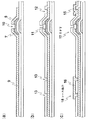
図8は、図7(c)におけるソース端子18を拡大して示した図であり、図8(a)がソース端子18の平面を、図8(b)が図8(a)の矢視B−B断面をそれぞれあらわしている。
【0011】
TFTアレイ基板の製造にあたっては、まず、絶縁性基板1の表面にたとえばCuやAlなどの金属膜をスパッタ法により成膜し、写真製版法により形成したレジストを用いてパターニングし、ゲート配線2を形成する(図6(a))。
【0012】
つぎに、プラズマCVD法によりゲート絶縁膜4となるシリコン窒化膜を全面に形成し(図6(b))、さらにアモルファスシリコン膜および不純物がドープされたn+型アモルファスシリコン膜を順次成膜したのち、写真製版法により形成したレジストを用いてアモルファスシリコン膜およびn+型アモルファスシリコン膜を同時にパターニングし、ゲート配線2の上方にTFTの半導体層5およびコンタクト層6を形成する(図6(c))。
【0013】
つぎに、図7(a)に示すように、ソース電極、ドレイン電極およびソース配線を形成するために、まずスパッタ法などにより、Cr膜もしくはAl膜などの金属膜を成膜し、写真製版法により形成したレジストを用いてパターニングし、ソース電極7、ドレイン電極8およびソース配線9を形成する。ついでドライエッチング法によりソース電極7およびドレイン電極8に覆われていない部分のn+アモルファスシリコン膜(コンタクト層6)をエッチングしてチャネル部10を形成する。
【0014】
つぎに、図7(b)に示すように、TFTを保護するために、プラズマCVD法などによりシリコン窒化膜を成膜して、パッシベーション膜11を形成する。その後、写真製版法により形成したレジストを用い、ドライエッチング法により、画素電極とドレイン電極8とを接続するためのコンタクトホール12と、ソース配線9と端子電極とを接続するためのコンタクトホール13を形成する。
【0015】
最後に、図7(c)に示すように、透明導電膜としてITO膜をスパッタ法などにより成膜したのち、写真製版法により形成したレジストを用いてパターニングし、画素電極15を形成すると同時に、外部信号源との接続のための端子電極16を形成する。
【0016】
このようにして製造したTFTアレイ基板について、ソース端子18の拡大図を図8に示す。すでに説明したように、ソース端子18の最上層には外部信号源との接続のための端子電極16が形成され、端子電極16はコンタクトホール13を介してソース配線9に接続されている。そして、ソース配線9の一端はTFT17のソース電極7へと接続されている。一方、ソース配線9のもう一端は、ショートリング23へと接続されている。
【0017】
製造工程の最終段階において、TFTアレイ基板の端部を切断位置24で切り落とし、さらに面取りをおこなってショートリング23を除去する。このときの面取り工程によって、基板端面においてソース配線9が剥離し、剥離した金属膜片同士が接触して、隣り合う端子同士を短絡させ隣接配線間のショートを引き起こすという問題があった。また、とくに切断位置を端子電極のすぐ近くとした場合や、製造装置の精度などによって切断位置が端子電極の近くにまでおよぶ場合などでは、剥離した金属膜片が隣の端子の端子電極に接触して、やはり隣接配線間のショートを引き起こすという問題があった。
【0018】
【発明が解決しようとする課題】
以上のように従来のTFTアレイ基板では、図8に示すように、ソース端子18において端子電極16の下層の金属層は、表示部側、ショートリング側ともすべて同層の金属層、すなわちソース配線9で形成されている。
【0019】
この構造においては、基板の切断および面取り工程時に切断位置24で基板の面取りを行なう場合、端子部端面のソース配線9が面取り工程によりはがれ、はがれた金属膜片同士が接触し、隣り合う端子同士を短絡させ、隣接配線間のショートを引き起こすなどの問題があった。また、はがれた金属膜片が端子電極に接触し、隣り合う端子同士を短絡させ隣接配線間のショートを引き起こすなどの問題があった。
【0020】
本発明は、叙上のような問題点を解消するためになされたもので、基板の切断および面取りによる金属層のはがれを防止して、信頼性の高い薄膜トランジスタアレイ基板を得ることを目的とする。
【0021】
【課題を解決するための手段】
本発明にかかわる薄膜トランジスタアレイ基板は、一対の基板間に液晶材料を挟持してなり、一方の基板に、画素電極と、該画素電極に電気的に接続されたスイッチング素子と、該スイッチング素子に電気的に接続されたゲート配線またはソース配線とを備える表示部が形成され、さらに該表示部の外側に、前記ゲート配線および前記ソース配線に外部信号源からの電気配線を接続するための端子部が形成されてなる薄膜トランジスタアレイ基板であって、前記端子部が、基板の最上層に位置し前記外部信号源からの電気配線が接続される端子電極と、該端子電極の下層に配置されコンタクトホールを介して該端子電極へと接続される第1の金属配線および第2の金属配線を有し、前記第1の金属配線は前記表示部側に形成され、前記第2の金属配線は基板端部側に形成され、前記第1の金属配線と前記第2の金属配線とは、あいだに絶縁膜が存在し、前記端子電極を介して接続されており、前記第1または第2の金属配線の一方が前記ソース配線と同層で形成され、他方の金属配線が前記ゲート配線と同層で形成され、前記第1の金属配線は前記絶縁膜より上層に形成され、前記第2の金属配線は前記絶縁膜より下層に形成され、前記基板端部まで延在していることを特徴とする。
【0022】
また、前記第2の金属配線が、切断または面取りがなされていることを特徴とする。
【0023】
また、第1の金属配線の一方がソース配線へと接続されていることを特徴とする。
【0024】
また、前記第1の金属配線が前記ゲート配線へと接続されていることを特徴とする。
また、前記端子電極の下層に配置され、前記端子電極と前記第1の金属配線を接続する前記コンタクトホールは、複数個であることを特徴とする。
また、前記端子電極の下層に配置され、前記端子電極と前記第1の金属配線を接続する前記コンタクトホールは、前記端子電極の前記表示部側の端部近傍と、前記第1の金属配線の前記基板端部側の端部近傍に設けられていることを特徴とする。
また、前記端子電極の中央近傍にはコンタクトホールは設けられていないことを特徴とする。
また、前記端子電極の前記基板端部側の端部近傍で、前記第2の金属配線の幅が細くなり、前記基板端部まで延在していることを特徴とする。
また、前記端子電極の下層に配置される前記第1の金属配線と前記第2の金属配線とは、平面視において、重なっていないことを特徴とする。
また、前記端子電極の下層に配置され、前記端子電極と前記第1の金属配線を接続する前記コンタクトホールと、前記端子電極と前記第2の金属配線を接続する前記コンタクトホールとは、異なる位置にあることを特徴とする。
【0025】
【発明の実施の形態】
実施の形態1
以下、本発明の一実施の形態について、図に基づいて説明する。
【0026】
図1,2は本発明の実施の形態1による薄膜トランジスタアレイ基板について、TFTおよびソース端子の製造工程を示す断面図である。
【0027】
図において、1はガラス基板などの透明な絶縁性基板、あるいは単なる絶縁性基板である。2,3はそれぞれ、基板1上に形成されたゲート配線、ショートリングへの取り出し配線であり、AlもしくはCrなどの金属層から形成される。4はゲート配線2および取り出し配線3上に基板1の全面にわたって形成されたゲート絶縁膜であり、シリコン窒化膜からなる。
【0028】
5はゲート絶縁膜4を介してゲート配線2の上方に形成された半導体層であり、アモルファスシリコン膜などからなる。6は半導体層5上に形成されたコンタクト層であり、n+型アモルファスシリコン膜からなる。7および8はそれぞれ、コンタクト層6上に形成されたソース電極、ドレイン電極であり、9はソース電極7およびドレイン電極8の形成と同時に形成されたソース配線、10はコンタクト層6を選択的にエッチングすることにより形成されたチャネル部である。11はTFT保護のためのパッシベーション膜であり、シリコン窒化膜からなる。
【0029】
12は、画素電極への接続のためにドレイン電極8上のパッシベーション膜11に形成されたコンタクトホール、13はソース配線9と端子電極とを接続するためにソース配線9上のパッシベーション膜11に形成されたコンタクトホール、14は端子電極と取り出し配線3とを接続するために、取り出し配線3上のゲート絶縁膜4およびパッシベーション膜11に形成されたコンタクトホールである。
【0030】
さらに、15はコンタクトホール12を介してドレイン電極8へと接続された画素電極であり、ITO膜からなる。16は画素電極15と同時に形成され、コンタクトホール13,14を介してソース配線9、取り出し配線3へと接続された端子電極である。
【0031】
図3は、図2(c)におけるソース端子18を拡大して示した図であり、図3(a)がソース端子18の平面を、図3(b)は図3(a)の矢視A−A断面をそれぞれあらわしている。
【0032】
つぎに、本実施の形態による薄膜トランジスタアレイ基板の製造方法を説明する。まず、図1(a)に示すように、絶縁性基板1の表面にたとえばCuやAlなどの金属膜をスパッタ法により成膜したあと、写真製版法より形成したレジストを用いてパターニングし、ゲート配線2およびショートリングへの取り出し配線3を形成する。
【0033】
Cr膜やAl膜などの金属膜のパターニングにはウェットエッチング法を用いるが、あらかじめエッチャントの組成を検討して、Cr膜やAl膜などの金属膜のエッチング端面をテーパ形状に形成することにより、この金属層の上層に形成する膜の被膜性を向上できる。
【0034】
つぎに、プラズマCVD法によりゲート絶縁膜4となるシリコン窒化膜を全面に形成し(図1(b))、さらにアモルファスシリコン膜と不純物がドープされたn+型アモルファスシリコン膜とを順次成膜したのち、写真製版法により形成したレジストを用いてアモルファスシリコン膜およびn+型アモルファスシリコン膜を同時にパターニングし、ゲート配線2の上方にTFTの半導体層5およびコンタクト層6を形成する(図1(c))。
【0035】
つぎに、図2(a)に示すように、ソース電極、ドレイン電極およびソース配線を形成するために、まずスパッタ法などにより、Cr膜もしくはAl膜などの金属膜を成膜し、写真製版法により形成したレジストを用いてパターニングし、ソース電極7、ドレイン電極8およびソース配線9を形成する。ついで、ドライエッチング法によりソース電極7およびドレイン電極8に覆われていない部分のn+型アモルファスシリコン膜(コンタクト層6)をエッチングしてチャネル部10を形成する。
【0036】
つぎに、図2(b)に示すように、TFTを保護するために、プラズマCVD法などによりシリコン窒化膜を成膜して、パッシベーション膜11を形成する。その後、写真製版法により形成したレジストを用い、ドライエッチング法により画素電極とドレイン電極8とを接続するためのコンタクトホール12と、ソース配線9と端子電極とを接続するためのコンタクトホール13と、端子電極と取り出し配線3とを接続するためのコンタクトホール14とを形成する。
【0037】
最後に、図2(c)に示すように、透明導電膜としてITO膜をスパッタ法などにより成膜したのち、写真製版法により形成したレジストを用いてパターニングし、画素電極15を形成すると同時に、端子電極16を形成する。
【0038】
したがって、ソース配線9は、コンタクトホール13、端子電極16およびコンタクトホール14を介して、ショートリングへの取り出し配線3に電気的に接続されている。
【0039】
以上の工程により形成されたTFTアレイ基板の表面にさらに配向膜を形成し、透明絶縁性基板上に遮光膜、対向電極、配向膜などを形成してなる対向基板を対向配置し、両基板のあいだに液晶材料を注入してシール材で封止し、そののちTFTアレイ基板の端部を切断してショートリング23を除去し、切断面の面取りを行なうことにより薄膜トランジスタアレイ基板を構成する。
【0040】
本実施の形態による薄膜トランジスタアレイ基板においては、図3のソース端子18の拡大図に示すように、端子部形成時に端子電極16の下層の金属配線を、表示部側と基板端部側とでそれぞれ別の金属層から形成する。つまり、表示部側の金属配線であるソース配線9はソース電極7やドレイン電極8と同一の金属層から形成され、基板端部側すなわちショートリング側の金属配線である取り出し配線3はゲート配線2と同一の金属層から形成される。
【0041】
本発明によれば、図3に示した切断位置24において、金属配線すなわち取り出し配線3がゲート絶縁膜4よりも下層にある。したがって、基板切断時の面取りによって取り出し配線3が削られることがなくなる、あるいは削られる量が少なくなり、金属膜片の発生を最小限に抑制することができる。また、上層に位置するゲート絶縁膜4が抑えの役割を果たすため、この点からも、取り出し配線3の剥離を抑制して金属膜片の発生を防ぎ、端子間短絡の発生を防止することができる。
【0042】
なお、本実施の形態では、ソース電極およびソース配線がゲート配線よりも上層に形成され、ソース端子での短絡が問題となるTFTアレイ基板を例として説明を行なった。しかし、ゲート配線がソース配線よりも上層に形成されているTFTアレイ基板であっても、本発明によって切断、面取り位置でのゲート配線端部の剥離を抑制して、端子間短絡を防止することが可能である。
【0043】
【発明の効果】
以上のように、本発明によれば、端子部で端子電極の下層に位置する金属配線において、基板端部側の金属配線を表示部側の金属配線と別層に形成しているため、基板の切断および面取り工程時に、金属配線がはがれて金属膜片を生じることを防ぎ、金属膜片による端子間ショートを防止して、より信頼性の高い薄膜トランジスタアレイ基板を得ることができる。また、切断および面取りを行なう位置を端子電極のすぐ近くとしても端子間ショートを生じることがないため、高精度の切断面取り設備が不要となる、薄膜トランジスタアレイ基板の小型化が可能となる、切断しろを小さくして材料の無駄を少なくすることができるなどの利点がある。
【図面の簡単な説明】
【図1】 本発明の実施の形態1による薄膜トランジスタアレイ基板の製造工程を示す断面図である。
【図2】 本発明の実施の形態1による薄膜トランジスタアレイ基板の製造工程を示す断面図であり、図1に続く工程を表わした図である。
【図3】 本発明の実施の形態1による薄膜トランジスタアレイ基板について、端子部を拡大して示した平面図、および断面図である。
【図4】 薄膜トランジスタアレイ基板の全体を示す概略平面図である。
【図5】 薄膜トランジスタアレイ基板を示す平面図であり、とくに表示部の画素を示す図である。
【図6】 従来の技術による薄膜トランジスタアレイ基板の製造工程を示す断面図である。
【図7】 従来の技術による薄膜トランジスタアレイ基板の製造工程を示す断面図である。
【図8】 従来の技術による薄膜トランジスタアレイ基板について、端子部を拡大して示した平面図、および断面図である。
【符号の説明】
1 基板
2 ゲート配線
3 ショートリングへの取り出し配線
4 ゲート絶縁膜
5 半導体層
6 コンタクト層
7 ソース電極
8 ドレイン電極
9 ソース配線
10 チャネル部
11 パッシベーション膜
12、13、14 コンタクトホール
15 画素電極
16 端子電極
17 TFT
18 ソース端子
19 ゲート端子
20、21 端子部
22 表示部
23 ショートリング
24 切断位置[0001]
BACKGROUND OF THE INVENTION
The present invention relates to a thin film transistor array substrate and a display device using the same , and more particularly to an active matrix type thin film transistor array substrate on which a thin film transistor (hereinafter also referred to as TFT) is mounted as a switching element.
[0002]
[Prior art]
The thin film transistor array substrate has a liquid crystal material sandwiched between a pair of substrates. FIG. 5 shows an enlarged plan view of one substrate. As shown in FIG. 5,
[0003]
FIG. 4 shows the entire plane of the TFT array substrate. The
[0004]
The
[0005]
Next, the manufacturing process of the TFT array substrate will be described with reference to FIGS. 6 and 7 show cross sections of TFTs and source terminals on the TFT array substrate.
[0006]
In the figure, reference numeral 1 denotes a transparent insulating substrate such as a glass substrate or a simple insulating substrate.
[0007]
A
[0008]
12 is a contact hole formed in the
[0009]
[0010]
8 is an enlarged view of the
[0011]
In manufacturing the TFT array substrate, first, a metal film such as Cu or Al is formed on the surface of the insulating substrate 1 by sputtering, patterned using a resist formed by photolithography, and the
[0012]
Next, a silicon nitride film to be the
[0013]
Next, as shown in FIG. 7A, in order to form a source electrode, a drain electrode, and a source wiring, first, a metal film such as a Cr film or an Al film is formed by a sputtering method or the like, and a photolithography process is performed. Patterning is performed using the resist formed by the above steps, and the
[0014]
Next, as shown in FIG. 7B, a
[0015]
Finally, as shown in FIG. 7C, after forming an ITO film as a transparent conductive film by sputtering or the like, patterning is performed using a resist formed by photolithography, and simultaneously forming the
[0016]
FIG. 8 shows an enlarged view of the
[0017]
In the final stage of the manufacturing process, the end of the TFT array substrate is cut off at the cutting position 24 and further chamfered to remove the short ring 23. Due to the chamfering process at this time, the
[0018]
[Problems to be solved by the invention]
As described above, in the conventional TFT array substrate, as shown in FIG. 8, the metal layer under the
[0019]
In this structure, when the substrate is chamfered at the cutting position 24 at the time of cutting and chamfering the substrate, the
[0020]
The present invention has been made to solve the above-described problems, and an object of the present invention is to obtain a highly reliable thin film transistor array substrate by preventing peeling of the metal layer due to cutting and chamfering of the substrate. .
[0021]
[Means for Solving the Problems]
A thin film transistor array substrate according to the present invention includes a liquid crystal material sandwiched between a pair of substrates, a pixel electrode on one substrate, a switching element electrically connected to the pixel electrode, and an electrical connection to the switching element. indication unit and a gate connected wiring or a source wiring is formed, further on the outside of the display unit, the terminal portions for connecting electrical wires from an external signal source to the gate wiring and the source wiring A thin film transistor array substrate formed, wherein the terminal portion is located on the uppermost layer of the substrate and is connected to an electrical wiring from the external signal source, and a contact hole disposed below the terminal electrode. A first metal wiring and a second metal wiring connected to the terminal electrode via the first metal wiring, the first metal wiring being formed on the display portion side, Genus wiring is formed on the substrate end part side, wherein the first metal wiring and the second metal wiring, an insulating film is present in between, is connected via the terminal electrode, the first or One of the second metal wirings is formed in the same layer as the source wiring, the other metal wiring is formed in the same layer as the gate wiring, the first metal wiring is formed in a layer above the insulating film, The second metal wiring is formed below the insulating film and extends to the end of the substrate .
[0022]
Further, the second metal wires, characterized in that the cutting or chamfering has been made.
[0023]
Further, one of the first metal wirings is connected to the source wiring.
[0024]
Further, the first metal wiring is connected to the gate wiring .
The contact hole may be disposed in a lower layer of the terminal electrode and connect the terminal electrode and the first metal wiring.
Further, the contact hole, which is disposed under the terminal electrode and connects the terminal electrode and the first metal wiring, is in the vicinity of the end portion of the terminal electrode on the display unit side, and the first metal wiring. It is provided in the vicinity of the end portion on the substrate end portion side.
The contact hole is not provided near the center of the terminal electrode.
Further, the width of the second metal wiring is narrow in the vicinity of the end portion of the terminal electrode on the substrate end portion side, and extends to the end portion of the substrate.
Further, the first metal wiring and the second metal wiring arranged in a lower layer of the terminal electrode do not overlap in a plan view.
Further, the contact hole, which is disposed under the terminal electrode and connects the terminal electrode and the first metal wiring, and the contact hole that connects the terminal electrode and the second metal wiring are different positions. It is characterized by that.
[0025]
DETAILED DESCRIPTION OF THE INVENTION
Embodiment 1
Hereinafter, an embodiment of the present invention will be described with reference to the drawings.
[0026]
1 and 2 are cross-sectional views showing the steps of manufacturing TFTs and source terminals for the thin film transistor array substrate according to Embodiment 1 of the present invention.
[0027]
In the figure, reference numeral 1 denotes a transparent insulating substrate such as a glass substrate or a simple insulating substrate.
[0028]
A
[0029]
12 is a contact hole formed in the
[0030]
[0031]
FIG. 3 is an enlarged view of the
[0032]
Next, a method for manufacturing the thin film transistor array substrate according to the present embodiment will be described. First, as shown in FIG. 1A, after a metal film such as Cu or Al is formed on the surface of the insulating substrate 1 by sputtering, patterning is performed using a resist formed by photolithography, and the gate The
[0033]
A wet etching method is used for patterning a metal film such as a Cr film or an Al film. However, by examining the composition of the etchant in advance and forming an etching end surface of the metal film such as a Cr film or an Al film in a tapered shape, The film property of the film formed on the metal layer can be improved.
[0034]
Next, a silicon nitride film to be the
[0035]
Next, as shown in FIG. 2A, in order to form a source electrode, a drain electrode, and a source wiring, first, a metal film such as a Cr film or an Al film is formed by a sputtering method or the like, and a photolithography process is performed. Patterning is performed using the resist formed by the above steps, and the
[0036]
Next, as shown in FIG. 2B, a
[0037]
Finally, as shown in FIG. 2 (c), after forming an ITO film as a transparent conductive film by a sputtering method or the like, patterning is performed using a resist formed by a photolithography method, and simultaneously forming the
[0038]
Accordingly, the
[0039]
An alignment film is further formed on the surface of the TFT array substrate formed by the above steps, and a counter substrate formed by forming a light shielding film, a counter electrode, an alignment film, etc. on the transparent insulating substrate is arranged to face each other. A thin film transistor array substrate is formed by injecting a liquid crystal material and sealing with a sealing material, and then cutting the end portion of the TFT array substrate to remove the short ring 23 and chamfering the cut surface.
[0040]
In the thin film transistor array substrate according to the present embodiment, as shown in the enlarged view of the
[0041]
According to the present invention, the metal wiring, that is, the
[0042]
In this embodiment, the TFT array substrate is described as an example in which the source electrode and the source wiring are formed in an upper layer than the gate wiring, and a short circuit at the source terminal is a problem. However, even if the gate wiring is a TFT array substrate formed in an upper layer than the source wiring, it is possible to prevent the short circuit between the terminals by suppressing the peeling of the edge of the gate wiring at the chamfered position by the present invention. Is possible.
[0043]
【The invention's effect】
As described above, according to the present invention, in the metal wiring located in the lower layer of the terminal electrode in the terminal portion, the metal wiring on the substrate end side is formed in a different layer from the metal wiring on the display portion side. During the cutting and chamfering steps, it is possible to prevent the metal wiring from being peeled off and form a metal film piece, prevent a short circuit between terminals due to the metal film piece, and obtain a more reliable thin film transistor array substrate . In addition, even if the cutting and chamfering positions are close to the terminal electrodes, there is no short circuit between the terminals, so that a highly accurate cutting chamfering facility is not required, and the thin film transistor array substrate can be downsized. There is an advantage that the waste of material can be reduced by reducing the size.
[Brief description of the drawings]
FIG. 1 is a cross-sectional view showing a manufacturing process of a thin film transistor array substrate according to a first embodiment of the present invention.
2 is a cross-sectional view showing a manufacturing process of the thin film transistor array substrate according to the first embodiment of the present invention, and is a view showing a process following FIG. 1. FIG.
FIGS. 3A and 3B are a plan view and a cross-sectional view showing an enlarged terminal portion of the thin film transistor array substrate according to the first embodiment of the present invention. FIGS.
FIG. 4 is a schematic plan view showing the entire thin film transistor array substrate.
FIG. 5 is a plan view showing a thin film transistor array substrate, in particular, a pixel of a display unit.
FIG. 6 is a cross-sectional view illustrating a manufacturing process of a thin film transistor array substrate according to a conventional technique.
FIG. 7 is a cross-sectional view illustrating a manufacturing process of a thin film transistor array substrate according to a conventional technique.
FIG. 8 is an enlarged plan view and a sectional view of a terminal portion of a conventional thin film transistor array substrate.
[Explanation of symbols]
1 Substrate
2 Gate wiring
3 Wiring to the short ring
4 Gate insulation film
5 Semiconductor layer
6 Contact layer
7 Source electrode
8 Drain electrode
9 Source wiring
10 channel section
11
15 Pixel electrode
16 terminal electrode
17 TFT
18 Source terminal
19 Gate terminal 20, 21 Terminal part
22 Display section
23 Short ring
24 Cutting position
Claims (11)
前記端子部が、前記外部信号源からの電気配線が接続される端子電極と、該端子電極の下層に配置されコンタクトホールを介して該端子電極へと接続される第1の金属配線および第2の金属配線を有し、前記第1の金属配線は前記表示部側に形成され、前記第2の金属配線は基板端部側に形成され、
前記第1の金属配線と前記第2の金属配線とは、あいだに絶縁膜が存在し、
前記端子電極を介して接続されており、
前記第1または第2の金属配線の一方が前記ソース配線と同層で形成され、他方の金属配線が前記ゲート配線と同層で形成され、
前記第1の金属配線は前記絶縁膜より上層に形成され、
前記第2の金属配線は前記絶縁膜より下層に形成され、前記基板端部まで延在していることを特徴とする薄膜トランジスタアレイ基板。A display portion including a pixel electrode, a switching element connected to the pixel electrode, and a gate wiring and a source wiring connected to the switching element is formed on the surface, and further, the gate wiring or A thin film transistor array substrate in which a terminal portion for connecting an electrical wiring from an external signal source to the source wiring is formed,
A terminal electrode to which an electrical wiring from the external signal source is connected; a first metal wiring disposed below the terminal electrode and connected to the terminal electrode through a contact hole; The first metal wiring is formed on the display unit side, the second metal wiring is formed on the substrate end side,
Wherein the first metal wiring and the second metal wiring, an insulating film is present in between,
Connected via the terminal electrode,
One of the first or second metal wiring is formed in the same layer as the source wiring, and the other metal wiring is formed in the same layer as the gate wiring,
The first metal wiring is formed above the insulating film,
The thin film transistor array substrate, wherein the second metal wiring is formed below the insulating film and extends to an end of the substrate.
Priority Applications (4)
| Application Number | Priority Date | Filing Date | Title |
|---|---|---|---|
| JP2001054854A JP4646420B2 (en) | 2001-02-28 | 2001-02-28 | Thin film transistor array substrate and display device using the same |
| TW091102576A TWI230821B (en) | 2001-02-28 | 2002-02-15 | Liquid crystal display device |
| KR1020020009728A KR100682691B1 (en) | 2001-02-28 | 2002-02-23 | Liquid crystal display |
| US10/082,984 US7872698B2 (en) | 2001-02-28 | 2002-02-25 | Liquid crystal display with structure resistant to exfoliation during fabrication |
Applications Claiming Priority (1)
| Application Number | Priority Date | Filing Date | Title |
|---|---|---|---|
| JP2001054854A JP4646420B2 (en) | 2001-02-28 | 2001-02-28 | Thin film transistor array substrate and display device using the same |
Publications (3)
| Publication Number | Publication Date |
|---|---|
| JP2002258319A JP2002258319A (en) | 2002-09-11 |
| JP2002258319A5 JP2002258319A5 (en) | 2008-01-31 |
| JP4646420B2 true JP4646420B2 (en) | 2011-03-09 |
Family
ID=18915123
Family Applications (1)
| Application Number | Title | Priority Date | Filing Date |
|---|---|---|---|
| JP2001054854A Expired - Lifetime JP4646420B2 (en) | 2001-02-28 | 2001-02-28 | Thin film transistor array substrate and display device using the same |
Country Status (4)
| Country | Link |
|---|---|
| US (1) | US7872698B2 (en) |
| JP (1) | JP4646420B2 (en) |
| KR (1) | KR100682691B1 (en) |
| TW (1) | TWI230821B (en) |
Families Citing this family (15)
| Publication number | Priority date | Publication date | Assignee | Title |
|---|---|---|---|---|
| JP4646420B2 (en) * | 2001-02-28 | 2011-03-09 | 三菱電機株式会社 | Thin film transistor array substrate and display device using the same |
| JP2004354798A (en) * | 2003-05-30 | 2004-12-16 | Nec Lcd Technologies Ltd | Thin film transistor substrate and its manufacturing method |
| JP4798336B2 (en) * | 2005-01-11 | 2011-10-19 | カシオ計算機株式会社 | Method for manufacturing circuit board device |
| JP4816110B2 (en) * | 2006-01-31 | 2011-11-16 | ソニー株式会社 | Liquid crystal display |
| JP4850589B2 (en) * | 2006-05-31 | 2012-01-11 | 株式会社 日立ディスプレイズ | Display device |
| TWI387807B (en) | 2008-08-11 | 2013-03-01 | Chunghwa Picture Tubes Ltd | Bonding pad, active device array substrate and liquid crystal display panel |
| KR101643835B1 (en) * | 2009-07-10 | 2016-07-28 | 가부시키가이샤 한도오따이 에네루기 켄큐쇼 | Semiconductor device and method for manufacturing the same |
| CN102662264B (en) * | 2012-04-28 | 2016-03-02 | 深圳市华星光电技术有限公司 | A kind of power-up circuit, crystal liquid substrate and a kind of liquid crystal panel method for making |
| CN102854643B (en) * | 2012-09-04 | 2015-11-25 | 深圳市华星光电技术有限公司 | A kind of display panels and manufacture method thereof |
| JP6364810B2 (en) * | 2014-02-26 | 2018-08-01 | セイコーエプソン株式会社 | Electro-optical device and method for manufacturing electro-optical device |
| KR102494779B1 (en) * | 2015-12-22 | 2023-02-02 | 엘지디스플레이 주식회사 | Liquid crystal display with touch |
| CN105607366B (en) * | 2016-01-05 | 2019-03-05 | 京东方科技集团股份有限公司 | Anti-static device and its manufacturing method, substrate |
| CN107422550B (en) * | 2017-07-24 | 2020-05-01 | 武汉华星光电技术有限公司 | Pin, manufacturing method thereof and display panel |
| CN108550580B (en) * | 2018-04-27 | 2019-10-11 | 武汉华星光电技术有限公司 | Tft array substrate |
| JP6729658B2 (en) * | 2018-10-16 | 2020-07-22 | セイコーエプソン株式会社 | Liquid crystal device and electronic equipment |
Citations (5)
| Publication number | Priority date | Publication date | Assignee | Title |
|---|---|---|---|---|
| JPH086059A (en) * | 1994-06-23 | 1996-01-12 | Nec Corp | Active matrix substrate |
| JPH11509938A (en) * | 1995-07-31 | 1999-08-31 | リットン システムズ カナダ リミテッド | Semiconductor switch array with electrostatic discharge prevention circuit and manufacturing method |
| JPH11288007A (en) * | 1998-02-20 | 1999-10-19 | Lg Lcd Inc | Liquid crystal display device and its manufacture |
| JPH11326942A (en) * | 1998-05-07 | 1999-11-26 | Mitsubishi Electric Corp | Liquid crystal display element, liquid crystal display device using the element, parallel electric field type liquid crystal display device, and reflection type liquid crystal display device |
| JP2001142096A (en) * | 1999-08-31 | 2001-05-25 | Fujitsu Ltd | Liquid crystal display device |
Family Cites Families (12)
| Publication number | Priority date | Publication date | Assignee | Title |
|---|---|---|---|---|
| JPS6419324U (en) | 1987-07-27 | 1989-01-31 | ||
| US5492582A (en) * | 1993-04-22 | 1996-02-20 | Casio Computer Co., Ltd. | Method of manufacturing liquid crystal display device |
| US5546204A (en) * | 1994-05-26 | 1996-08-13 | Honeywell Inc. | TFT matrix liquid crystal device having data source lines and drain means of etched and doped single crystal silicon |
| TW347477B (en) * | 1994-09-30 | 1998-12-11 | Sanyo Electric Co | Liquid crystal display with storage capacitors for holding electric charges |
| JP3315834B2 (en) * | 1995-05-31 | 2002-08-19 | 富士通株式会社 | Thin film transistor matrix device and method of manufacturing the same |
| KR100338480B1 (en) * | 1995-08-19 | 2003-01-24 | 엘지.필립스 엘시디 주식회사 | Liquid crystal display and method for fabricating the same |
| JPH09113931A (en) * | 1995-10-16 | 1997-05-02 | Sharp Corp | Liquid crystal display device |
| KR0161462B1 (en) * | 1995-11-23 | 1999-01-15 | 김광호 | Gate-pad forming method of liquid crystal display |
| JP3208658B2 (en) * | 1997-03-27 | 2001-09-17 | 株式会社アドバンスト・ディスプレイ | Manufacturing method of electro-optical element |
| TW440736B (en) * | 1997-10-14 | 2001-06-16 | Samsung Electronics Co Ltd | Liquid crystal displays and manufacturing methods thereof |
| JP3975008B2 (en) | 1998-07-21 | 2007-09-12 | 株式会社アドバンスト・ディスプレイ | Manufacturing method of display device |
| JP4646420B2 (en) * | 2001-02-28 | 2011-03-09 | 三菱電機株式会社 | Thin film transistor array substrate and display device using the same |
-
2001
- 2001-02-28 JP JP2001054854A patent/JP4646420B2/en not_active Expired - Lifetime
-
2002
- 2002-02-15 TW TW091102576A patent/TWI230821B/en not_active IP Right Cessation
- 2002-02-23 KR KR1020020009728A patent/KR100682691B1/en not_active IP Right Cessation
- 2002-02-25 US US10/082,984 patent/US7872698B2/en active Active
Patent Citations (5)
| Publication number | Priority date | Publication date | Assignee | Title |
|---|---|---|---|---|
| JPH086059A (en) * | 1994-06-23 | 1996-01-12 | Nec Corp | Active matrix substrate |
| JPH11509938A (en) * | 1995-07-31 | 1999-08-31 | リットン システムズ カナダ リミテッド | Semiconductor switch array with electrostatic discharge prevention circuit and manufacturing method |
| JPH11288007A (en) * | 1998-02-20 | 1999-10-19 | Lg Lcd Inc | Liquid crystal display device and its manufacture |
| JPH11326942A (en) * | 1998-05-07 | 1999-11-26 | Mitsubishi Electric Corp | Liquid crystal display element, liquid crystal display device using the element, parallel electric field type liquid crystal display device, and reflection type liquid crystal display device |
| JP2001142096A (en) * | 1999-08-31 | 2001-05-25 | Fujitsu Ltd | Liquid crystal display device |
Also Published As
| Publication number | Publication date |
|---|---|
| JP2002258319A (en) | 2002-09-11 |
| US7872698B2 (en) | 2011-01-18 |
| KR100682691B1 (en) | 2007-02-15 |
| TWI230821B (en) | 2005-04-11 |
| KR20020070810A (en) | 2002-09-11 |
| US20020130983A1 (en) | 2002-09-19 |
Similar Documents
| Publication | Publication Date | Title |
|---|---|---|
| US6562645B2 (en) | Method of fabricating fringe field switching mode liquid crystal display | |
| US6927105B2 (en) | Thin film transistor array substrate and manufacturing method thereof | |
| JP4646420B2 (en) | Thin film transistor array substrate and display device using the same | |
| JP2005242372A (en) | Liquid crystal display device and method of manufacturing liquid crystal display device | |
| KR100673331B1 (en) | Liquid crystal display and method for fabricating the same | |
| JP4117369B2 (en) | Active matrix liquid crystal display device | |
| US6436743B1 (en) | Method of preventing electrical shorts | |
| US5466620A (en) | Method for fabricating a liquid crystal display device | |
| JP3600112B2 (en) | Manufacturing method of liquid crystal display device | |
| JP2000164874A (en) | Thin-film transistor array substrate, manufacturing method for it, and liquid-crystal display device | |
| JP3761756B2 (en) | Liquid crystal display device and manufacturing method thereof | |
| KR19980075975A (en) | Method for manufacturing thin film transistor substrate | |
| JP2004013003A (en) | Liquid crystal display | |
| JP4252126B2 (en) | Manufacturing method of liquid crystal display device | |
| JP2006163244A (en) | Thin film transistor array substrate, electro-optic display device, and method of manufacturing thin film transistor array substrate | |
| KR20070102384A (en) | Manufacturing method of pixel stucture | |
| KR100339334B1 (en) | the Structure of the LCD Pad and the Method for fabricating it | |
| JPH11194361A (en) | Manufacture of thin film transistor array substrate and liquid crystl display device | |
| US6462793B1 (en) | Liquid crystal display device and method of fabricating the same | |
| JP3941246B2 (en) | Manufacturing method of semiconductor device | |
| KR101023323B1 (en) | Lcd and method for manufacturing lcd | |
| US20060054889A1 (en) | Thin film transistor array panel | |
| JP2000035592A (en) | Liquid crystal display device | |
| JP3873164B2 (en) | Manufacturing method of active matrix type liquid crystal display panel | |
| JP3773834B2 (en) | Liquid crystal display |
Legal Events
| Date | Code | Title | Description |
|---|---|---|---|
| A711 | Notification of change in applicant |
Free format text: JAPANESE INTERMEDIATE CODE: A711 Effective date: 20071106 |
|
| A521 | Written amendment |
Free format text: JAPANESE INTERMEDIATE CODE: A523 Effective date: 20071113 |
|
| A621 | Written request for application examination |
Free format text: JAPANESE INTERMEDIATE CODE: A621 Effective date: 20071113 |
|
| RD03 | Notification of appointment of power of attorney |
Free format text: JAPANESE INTERMEDIATE CODE: A7423 Effective date: 20100609 |
|
| A977 | Report on retrieval |
Free format text: JAPANESE INTERMEDIATE CODE: A971007 Effective date: 20100629 |
|
| A131 | Notification of reasons for refusal |
Free format text: JAPANESE INTERMEDIATE CODE: A131 Effective date: 20100720 |
|
| A521 | Written amendment |
Free format text: JAPANESE INTERMEDIATE CODE: A523 Effective date: 20100915 |
|
| TRDD | Decision of grant or rejection written | ||
| A01 | Written decision to grant a patent or to grant a registration (utility model) |
Free format text: JAPANESE INTERMEDIATE CODE: A01 Effective date: 20101130 |
|
| A01 | Written decision to grant a patent or to grant a registration (utility model) |
Free format text: JAPANESE INTERMEDIATE CODE: A01 |
|
| A61 | First payment of annual fees (during grant procedure) |
Free format text: JAPANESE INTERMEDIATE CODE: A61 Effective date: 20101207 |
|
| FPAY | Renewal fee payment (event date is renewal date of database) |
Free format text: PAYMENT UNTIL: 20131217 Year of fee payment: 3 |
|
| R150 | Certificate of patent or registration of utility model |
Ref document number: 4646420 Country of ref document: JP Free format text: JAPANESE INTERMEDIATE CODE: R150 Free format text: JAPANESE INTERMEDIATE CODE: R150 |
|
| R250 | Receipt of annual fees |
Free format text: JAPANESE INTERMEDIATE CODE: R250 |
|
| R250 | Receipt of annual fees |
Free format text: JAPANESE INTERMEDIATE CODE: R250 |
|
| R250 | Receipt of annual fees |
Free format text: JAPANESE INTERMEDIATE CODE: R250 |
|
| R250 | Receipt of annual fees |
Free format text: JAPANESE INTERMEDIATE CODE: R250 |
|
| R250 | Receipt of annual fees |
Free format text: JAPANESE INTERMEDIATE CODE: R250 |
|
| R250 | Receipt of annual fees |
Free format text: JAPANESE INTERMEDIATE CODE: R250 |
|
| EXPY | Cancellation because of completion of term |