JP4570811B2 - Semiconductor device - Google Patents
Semiconductor device Download PDFInfo
- Publication number
- JP4570811B2 JP4570811B2 JP2001131542A JP2001131542A JP4570811B2 JP 4570811 B2 JP4570811 B2 JP 4570811B2 JP 2001131542 A JP2001131542 A JP 2001131542A JP 2001131542 A JP2001131542 A JP 2001131542A JP 4570811 B2 JP4570811 B2 JP 4570811B2
- Authority
- JP
- Japan
- Prior art keywords
- region
- film
- gate electrode
- transistor
- contact
- Prior art date
- Legal status (The legal status is an assumption and is not a legal conclusion. Google has not performed a legal analysis and makes no representation as to the accuracy of the status listed.)
- Expired - Fee Related
Links
Images


Classifications
-
- H—ELECTRICITY
- H10—SEMICONDUCTOR DEVICES; ELECTRIC SOLID-STATE DEVICES NOT OTHERWISE PROVIDED FOR
- H10B—ELECTRONIC MEMORY DEVICES
- H10B10/00—Static random access memory [SRAM] devices
-
- H—ELECTRICITY
- H10—SEMICONDUCTOR DEVICES; ELECTRIC SOLID-STATE DEVICES NOT OTHERWISE PROVIDED FOR
- H10D—INORGANIC ELECTRIC SEMICONDUCTOR DEVICES
- H10D84/00—Integrated devices formed in or on semiconductor substrates that comprise only semiconducting layers, e.g. on Si wafers or on GaAs-on-Si wafers
- H10D84/01—Manufacture or treatment
- H10D84/0123—Integrating together multiple components covered by H10D12/00 or H10D30/00, e.g. integrating multiple IGBTs
- H10D84/0126—Integrating together multiple components covered by H10D12/00 or H10D30/00, e.g. integrating multiple IGBTs the components including insulated gates, e.g. IGFETs
- H10D84/0165—Integrating together multiple components covered by H10D12/00 or H10D30/00, e.g. integrating multiple IGBTs the components including insulated gates, e.g. IGFETs the components including complementary IGFETs, e.g. CMOS devices
- H10D84/017—Manufacturing their source or drain regions, e.g. silicided source or drain regions
-
- H—ELECTRICITY
- H10—SEMICONDUCTOR DEVICES; ELECTRIC SOLID-STATE DEVICES NOT OTHERWISE PROVIDED FOR
- H10B—ELECTRONIC MEMORY DEVICES
- H10B99/00—Subject matter not provided for in other groups of this subclass
-
- H—ELECTRICITY
- H10—SEMICONDUCTOR DEVICES; ELECTRIC SOLID-STATE DEVICES NOT OTHERWISE PROVIDED FOR
- H10D—INORGANIC ELECTRIC SEMICONDUCTOR DEVICES
- H10D84/00—Integrated devices formed in or on semiconductor substrates that comprise only semiconducting layers, e.g. on Si wafers or on GaAs-on-Si wafers
- H10D84/01—Manufacture or treatment
- H10D84/02—Manufacture or treatment characterised by using material-based technologies
- H10D84/03—Manufacture or treatment characterised by using material-based technologies using Group IV technology, e.g. silicon technology or silicon-carbide [SiC] technology
- H10D84/038—Manufacture or treatment characterised by using material-based technologies using Group IV technology, e.g. silicon technology or silicon-carbide [SiC] technology using silicon technology, e.g. SiGe
-
- H—ELECTRICITY
- H10—SEMICONDUCTOR DEVICES; ELECTRIC SOLID-STATE DEVICES NOT OTHERWISE PROVIDED FOR
- H10D—INORGANIC ELECTRIC SEMICONDUCTOR DEVICES
- H10D84/00—Integrated devices formed in or on semiconductor substrates that comprise only semiconducting layers, e.g. on Si wafers or on GaAs-on-Si wafers
- H10D84/80—Integrated devices formed in or on semiconductor substrates that comprise only semiconducting layers, e.g. on Si wafers or on GaAs-on-Si wafers characterised by the integration of at least one component covered by groups H10D12/00 or H10D30/00, e.g. integration of IGFETs
- H10D84/82—Integrated devices formed in or on semiconductor substrates that comprise only semiconducting layers, e.g. on Si wafers or on GaAs-on-Si wafers characterised by the integration of at least one component covered by groups H10D12/00 or H10D30/00, e.g. integration of IGFETs of only field-effect components
- H10D84/83—Integrated devices formed in or on semiconductor substrates that comprise only semiconducting layers, e.g. on Si wafers or on GaAs-on-Si wafers characterised by the integration of at least one component covered by groups H10D12/00 or H10D30/00, e.g. integration of IGFETs of only field-effect components of only insulated-gate FETs [IGFET]
- H10D84/85—Complementary IGFETs, e.g. CMOS
-
- Y—GENERAL TAGGING OF NEW TECHNOLOGICAL DEVELOPMENTS; GENERAL TAGGING OF CROSS-SECTIONAL TECHNOLOGIES SPANNING OVER SEVERAL SECTIONS OF THE IPC; TECHNICAL SUBJECTS COVERED BY FORMER USPC CROSS-REFERENCE ART COLLECTIONS [XRACs] AND DIGESTS
- Y10—TECHNICAL SUBJECTS COVERED BY FORMER USPC
- Y10S—TECHNICAL SUBJECTS COVERED BY FORMER USPC CROSS-REFERENCE ART COLLECTIONS [XRACs] AND DIGESTS
- Y10S257/00—Active solid-state devices, e.g. transistors, solid-state diodes
- Y10S257/903—FET configuration adapted for use as static memory cell
- Y10S257/904—FET configuration adapted for use as static memory cell with passive components,, e.g. polysilicon resistors
Landscapes
- Semiconductor Memories (AREA)
- Static Random-Access Memory (AREA)
- Insulated Gate Type Field-Effect Transistor (AREA)
Description
【0001】
【発明の属する技術分野】
本発明は、SRAM(スタティックランダムアクセスメモリ:Static Random Access Memory)を有する半導体装置に関する。
【0002】
【従来の技術】
半導体記憶素子であるSRAMセルの基本的な構造について図面を用いて説明する。
【0003】
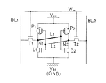
SRAMセルは、図1の回路図に示すように、情報蓄積部としてのフリップフロップ回路、及び情報の書き込み・読み出しを行うデータ線(ビット線BL1、BL2)とフリップフロップ回路との導通を制御する一対の転送トランジスタT1、T2で構成されている。そして、フリップフロップ回路は、例えば一対のCMOSインバータで構成され、それぞれのCMOSインバータは、一つの駆動トランジスタD1(D2)と一つの負荷トランジスタP1(P2)で構成される。
【0004】
転送トランジスタT1(T2)のソース/ドレイン領域の一方は、負荷トランジスタP1(P2)及び駆動トランジスタD1(D2)のドレインに接続され、他方はビット線BL1(BL2)に接続されている。また、一対の転送トランジスタT1、T2のゲートはそれぞれワード線WLの一部を構成し、互いに接続されている。
【0005】
CMOSインバータの一方を構成する駆動トランジスタD1及び負荷トランジスタP1のゲートは、他方のCMOSインバータを構成する駆動トランジスタD2及び負荷トランジスタP2のドレイン(蓄積ノードN2)に接続されている。また、この他方のCMOSインバータを構成する駆動トランジスタD2及び負荷トランジスタP2のゲートは、前記一方のCMOSインバータを構成する駆動トランジスタD1及び負荷トランジスタP1のドレイン(蓄積ノードN1)に接続されている。このように、一対のCMOSインバータ間において、一方のCMOSインバータの入出力部と他方のCMOSインバータのゲートとが互いにローカル配線(局所配線)と呼ばれる一対の配線L1、L2を介してクロスカップル(交差結合)されている。
【0006】
そして、駆動トランジスタD1、D2のソース領域には、基準電圧(Vss、例えばGND)が供給され、負荷トランジスタP1、P2のソース領域には、電源電圧(Vcc)が供給される。
【0007】
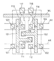
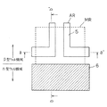
図2に、図1の回路図に相応する従来の一般的なSRAMセルのレイアウト図を示す。
【0008】
図中のARは活性領域を示し、各トランジスタを構成する不純物拡散領域が形成される。また、図中の一点鎖線で示す範囲が1メモリセルの範囲であり、各メモリセルはワード線WLの長手方向に沿って隣接配置され、この長手方向に垂直な方向にも繰り返し配置される。
【0009】
符号117及び118はそれぞれビット線BL1及びBL2へのコンタクトを示し、符号121及び122はそれぞれ電源電圧線へのコンタクトを示し、符号123及び124はそれぞれ基準電圧線(グランド線)へのコンタクトを示す。コンタクト116と111と113とは図示していないローカル配線L1で接続され、コンタクト115と112と114とは図示していないローカル配線L2で接続されている。コンタクト113と117との間のワード線WLの一部とその両側の拡散領域とで転送トランジスタT1が形成され、コンタクト114と118との間のワード線WLの一部とその両側の拡散領域とで転送トランジスタT2が形成される。コンタクト113と123との間の配線131の一部とその両側の拡散領域とで駆動トランジスタD1が形成され、コンタクト114と124との間の配線132の一部とその両側の拡散領域とで駆動トランジスタD2が形成される。コンタクト111と121との間の配線131の一部とその両側の拡散領域とで負荷トランジスタP1が形成され、コンタクト112と122との間の配線132の一部とその両側の拡散領域とで負荷トランジスタP2が形成される。
【0010】
以上に説明したSRAMセルは、ノイズに強く、待機時の消費電力が小さい等の優れた素子特性を有する。また、従来、この種のSRAMセルは、素子特性の点から、できるだけ素子構造の対称性を損なわないように(すなわち、アンバランス性を抑えるように)材料の選択やレイアウトがなされている。
【0011】
しかし、このようなSRAMは、1メモリセルに6トランジスタが必要なこと、多数の配線が必要なこと、及び同一セル内にp型MOSFETとn型MOSFETの素子分離が必要であること等から、セル面積が大きくなりやすいという問題を有している。
【0012】
そのため、このようなSRAMを有する半導体記憶装置においては、特に集積度の向上が重要な課題である。メモリセルについてのわずかな縮小であっても高集積度の半導体記憶装置全体としてはその集積度を大きく向上することができるため、メモリセルの面積を可能な限り小さくすることが重要である。そのため、近年の製造技術の進歩とあいまって、加工サイズの微細化やレイアウトの工夫とともに、配線同士の間隔や配線とコンタクトとの間隔の一層の縮小化が図られている。
【0013】
【発明が解決しようとする課題】
しかしながら、トランジスタのゲート電極と不純物拡散領域上のコンタクトとの間隔を小さくしすぎると、リークが発生するという問題が生じる。この現象は、負荷トランジスタP1、P2を構成するp型MOSFETにおいて顕著であり、リークの発生によりメモリセルのスタンバイ電流(待機時電流)が増大する。このような現象は、特に低消費電力(Low Power)型のSRAMにおいて問題となる。
【0014】
リークの発生は、ソース/ドレイン領域へのコンタクトがLDD(Lightly Doped Drain)領域に接している場合に顕著であり、その一つの要因として、LDD領域中の不純物がコンタクト側に吸収されることが考えられる。LDD領域は、高濃度の不純物拡散層であるソース/ドレイン領域に比べて不純物濃度が低いため、不純物の吸収の影響を受けやすく容易に不純物濃度が変化し、所望の接合が形成できなくなると考えられる。
【0015】
また、p型MOSFETにおいてリークが顕著である理由は、p型不純物として用いられたボロンが吸収されやすいためと考えられ、特にコンタクトを構成するバリア膜にチタン系金属膜を用いたときにリークが顕著であった。これは、チタン系金属膜とシリコン基板との接触界面において製造時の熱処理の影響によりチタンシリサイド層が形成され、主にこのチタンシリサイド層によりボロンの吸収が行われるためと考えられる。
【0016】
一方、シート抵抗やコンタクトとの接続抵抗を低減する目的で、ソース/ドレイン領域を構成する不純物拡散領域上には高融点金属シリサイド層が設けられる。特開平6−177067号公報には、このような構成、特に不純物イオンとしてボロンイオンが注入された不純物拡散層上にチタンシリサイド層が形成された構成において、不純物拡散層中のボロンがチタンシリサイド層に吸収され低濃度層が形成される問題が記載されている。同公報には、再度の不純物イオン注入を行って低濃度層における不純物濃度の低下分を補足し、非オーミックな特性や寄生抵抗の増大を抑制している。
【0017】
しかし、不純物濃度が低く且つ浅い接合を形成するLDD領域に対して、予め予測した不純物濃度の低下分を再度のイオン注入により精度よく補足することは困難である。また、このようなLDD領域の形成に際して、不純物濃度の低下分を見越した高い濃度設定を精度良く行うことも困難である。さらに、前記公報にも記載されているように、不純物の吸収により形成される低濃度層は接触界面近傍に発生するため、接合部分では高い濃度のままであり、このような濃度分布をもつLDD領域が形成されるとLDD構造本来の機能の発現が困難となり素子特性が低下する。
【0018】
そこで本発明の目的は、リークの発生を抑えながらメモリセル面積を低減可能な技術を実現し、素子特性に優れた高集積度の半導体記憶装置を提供することにある。
【0019】
【課題を解決するための手段】
本発明は、半導体基板の第1導電型ウェル上にゲート絶縁膜を介して形成されたゲート電極と、前記ゲート電極の両側にそれぞれ形成された、低濃度の第2導電型不純物拡散領域であるLDD領域および高濃度の第2導電型不純物拡散領域であるソース/ドレイン領域からなるLDD構造と、前記のゲート電極およびLDD構造部を覆う層間絶縁膜と、前記層間絶縁膜に形成された開口に導電性材料が埋め込まれてなるコンタクトを有する半導体装置において、
前記第1導電型ウェルと等電位となる一方のソース/ドレイン領域に接続するコンタクトが、このソース/ドレイン領域側のLDD領域に接し、且つ
前記第1導電型ウェルと異なる電位となる他方のソース/ドレイン領域に接続するコンタクトが、このソース/ドレイン領域側のLDD領域に接しないように配置されていることを特徴とする半導体装置に関する。
【0020】
また本発明は、一対の駆動トランジスタ及び一対の負荷トランジスタからなるフリップフロップ回路と一対の転送トランジスタとでメモリセルを構成するSRAMを有する半導体装置において、
前記負荷トランジスタは、半導体基板上にゲート絶縁膜を介して形成されたゲート電極と、前記ゲート電極の両側にそれぞれ形成された、低濃度の不純物拡散領域であるLDD領域および高濃度の不純物拡散領域であるソース/ドレイン領域からなるLDD構造を有し、
ソース領域に接続するコンタクトとゲート電極とのゲート長方向の間隔が、ゲート電極とソース領域間のゲート長方向のLDD領域幅より小さく、且つ
ドレイン領域に接続するコンタクトがドレイン領域側のLDD領域に接しないように配置されていることを特徴とする半導体装置に関する。
【0021】
また本発明は、一対の駆動トランジスタ及び一対の負荷トランジスタからなるフリップフロップ回路と一対の転送トランジスタとでメモリセルを構成するSRAMを有する半導体装置において、
前記負荷トランジスタ及び前記駆動トランジスタは、半導体基板上にゲート絶縁膜を介して形成されたゲート電極と、前記ゲート電極の両側にそれぞれ形成された、低濃度の不純物拡散領域であるLDD領域および高濃度の不純物拡散領域であるソース/ドレイン領域からなるLDD構造を有し、
ソース領域に接続するコンタクトとゲート電極とのゲート長方向の間隔が、ゲート電極とソース領域間のゲート長方向のLDD領域幅より小さく、且つ
ドレイン領域に接続するコンタクトがドレイン領域側のLDD領域に接しないように配置されていることを特徴とする半導体装置に関する。
【0022】
また本発明は、前記転送トランジスタが、半導体基板上にゲート絶縁膜を介して形成されたゲート電極と、前記ゲート電極の両側にそれぞれ形成された、低濃度の不純物拡散領域であるLDD領域および高濃度の不純物拡散領域であるソース/ドレイン領域からなるLDD構造を有し、
ソース/ドレイン領域に接続するコンタクトが、そのソース/ドレイン領域側のLDD領域に接しないように配置されている上記の半導体装置に関する。
【0023】
また本発明は、前記コンタクトが少なくともその底部がチタン或いはチタン含有材料で構成されている上記の半導体装置に関する。
【0024】
また本発明は、前記負荷トランジスタの不純物拡散領域がボロンを含有する上記の半導体装置に関する。
【0025】
また本発明は、前記の負荷トランジスタ、駆動トランジスタ及び転送トランジスタのそれぞれのソース/ドレイン領域の表面に高融点金属シリサイド層が形成されている上記の半導体装置に関する。
【0026】
また本発明は、前記一対の負荷トランジスタの一方の第1負荷トランジスタのドレイン領域に接続するコンタクトが、この第1負荷トランジスタのゲート電極と共通の第1導電膜配線Aで構成されるゲート電極を持つ第1駆動トランジスタのドレイン領域に接続するコンタクトと一体に形成され、層間絶縁膜である第1絶縁膜に設けられた埋込溝配線であり、
前記埋込溝配線は、前記フリップフロップ回路の一対の入出力端子間を交差結合する一対のローカル配線の一方を構成し、
前記第1絶縁膜上に第2絶縁膜を介して設けられた第2導電膜で形成された第2導電膜配線で、前記一対のローカル配線の他方が構成されていることを特徴とする上記の半導体装置に関する。
【0027】
また本発明は、前記第2導電膜配線が、前記埋込溝配線の上面の少なくとも一部と前記第2絶縁膜を介して重なるように配置され、前記埋込溝配線と前記第2導電膜配線とそれらの間に介在する前記第2絶縁膜とで容量素子が構成されている上記の半導体装置に関する。
【0028】
また本発明は、前記埋込溝配線が、前記一対の駆動トランジスタのうちの一方の前記第1駆動トランジスタのドレイン領域と、前記一対の負荷トランジスタのうちの一方の前記第1負荷トランジスタのドレイン領域と、他方の第2駆動トランジスタ及び他方の第2負荷トランジスタのゲート電極を構成する第1導電膜配線Bとに接続するように配置され、
前記第2導電膜配線が、前記第1駆動トランジスタ及び前記第1負荷トランジスタのゲート電極を構成する前記第1導電膜配線Aに接続するコンタクトと、前記第2駆動トランジスタのドレイン領域に接続するコンタクトと、前記第2負荷トランジスタのドレイン領域に接続するコンタクトとに接している上記の半導体装置に関する。
【0029】
【発明の実施の形態】
本発明の主な特徴の一つは、LDD構造を持つMOS型電界効果トランジスタ(MOSFET)におけるソース/ドレイン領域に接続するコンタクトとゲート電極とのゲート長方向の間隔に関わる特定のレイアウト構造にある。このような構造を有するMOSFETは、SRAMをはじめとする高集積度の半導体装置を構成するトランジスタとして好適である。
【0030】
以下、本発明の好適な実施の形態として、本発明をSRAMに適用した例を説明する。
【0031】
本実施形態のSRAMのメモリセルは、前述の図1に示すように、ワード線WLと一対のビット線BL1、BL2との交差部に配置され、一対の駆動トランジスタD1、D2と一対の負荷トランジスタP1、P2と一対の転送トランジスタT1、T2で構成されている。ここで、一対の駆動トランジスタD1、D2と一対の転送トランジスタT1、T2はnチャネル型で構成され、一対の負荷トランジスタP1、P2はpチャネル型で構成されている。
【0032】
一対の駆動トランジスタD1、D2と一対の負荷トランジスタP1、P2は、1ビットの情報を記憶する情報蓄積部としてのフリップフロップ回路を構成している。このフリップフロップ回路は、一対のCMOSインバータで構成され、それぞれのCMOSインバータは、一つの駆動トランジスタD1(D2)と一つの負荷トランジスタP1(P2)で構成される。
【0033】
転送トランジスタT1(T2)のソース/ドレイン領域の一方は、負荷トランジスタP1(P2)及び駆動トランジスタD1(D2)のドレインに接続され、他方はビット線BL1(BL2)に接続されている。また、一対の転送トランジスタT1、T2のゲートはそれぞれワード線WLの一部を構成し、互いに接続されている。
【0034】
CMOSインバータの一方を構成する駆動トランジスタD1及び負荷トランジスタP1のゲートは、他方のCMOSインバータを構成する駆動トランジスタD2及び負荷トランジスタP2のドレイン(蓄積ノードN2)に接続されている。また、この他方のCMOSインバータを構成する駆動トランジスタD2及び負荷トランジスタP2のゲートは、前記一方のCMOSインバータを構成する駆動トランジスタD1及び負荷トランジスタP1のドレイン(蓄積ノードN1)に接続されている。このように、一対のCMOSインバータ間において、一方のCMOSインバータの入出力部(蓄積ノード)と他方のCMOSインバータのゲートとが互いにローカル配線(局所配線)と呼ばれる一対の配線L1、L2を介してクロスカップル(交差結合)されている。
【0035】
そして、駆動トランジスタD1、D2のソース領域には、基準電圧(Vss、例えばGND)が供給され、負荷トランジスタP1、P2のソース領域には、電源電圧(Vcc)が供給される。
【0036】
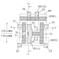
次に、図3及び図4を用いて、LDD構造を持つMOSFETにおけるソース/ドレイン領域に接続するコンタクトとゲート電極とのゲート長方向の間隔に関わる特定のレイアウト構造の一実施形態について説明する。
【0037】
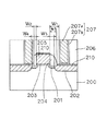
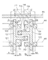
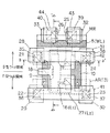
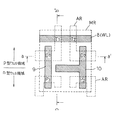
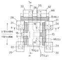
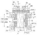
図3に、本実施形態のSRAMセルを構成する駆動トランジスタ及び負荷トランジスタの模式的な断面構造を示し、図4にSRAMセルのレイアウト図を示す。なお、図4中、前述の図2と同じ箇所については同じ符号を用いている。
【0038】
素子分離絶縁膜(不図示)により分離されたシリコン半導体基板200の活性領域上にゲート絶縁膜203を介してゲート電極205が形成されており、その両側にサイドウォール絶縁膜204が形成されている。
【0039】
また、ゲート電極205の両側の半導体基板中にはそれぞれ不純物を低濃度に含有する不純物拡散領域であるLDD領域201と高濃度に含有する不純物拡散領域であるソース/ドレイン領域202が形成され、LDD構造が設けられている。p型不純物としてはホウ素が含有され、n型不純物としてはリンやヒ素が含有される。ソース/ドレイン領域の不純物のドース量は、1×1015〜8×1015 atoms/cm2 に設定でき、LDD領域の不純物のドース量は、1×10¹³〜2×10¹⁴ atoms/cm2 に設定することができる。特にLDD領域の不純物のドース量は、不純物拡散領域の接合界面での電界上昇によるオフ時電流の上昇を抑制する点から前記の範囲に設定することが好ましい。また、ソース/ドレイン領域の接合深さは0.1〜0.2μmに設定することができる。LDD領域の接合深さは、n型MOSFETにおいては0.02〜0.05μm、p型MOSFETにおいては0.03〜0.06μmに設定することができる。
【0040】
ゲート電極205のゲート長は0.18〜0.20μmに設定することができ、サイドウォール絶縁膜204の幅W5(ゲート長方向の長さ)は0.09〜0.13μmに設定することができる。サイドウォール絶縁膜の幅W5が狭すぎると製造上LDD領域が小さくなりLDD構造の電界抑制効果が低下する。サイドウォール絶縁膜の幅W5が大き過ぎると、LDD領域が長くなり抵抗が大きくなるためトランジスタ特性が低下する。以上の構成でMOSFETが形成されている。
【0041】
上記MOSFETにおいて、ソース/ドレイン領域202及びゲート電極205上には抵抗値を下げるために高融点金属シリサイド層210が形成されている。この高融点金属シリサイド層としては、チタンシリサイド層やコバルトシリサイド層を用いることができるが、シリサイド層の抵抗およびボロン吸収性の点から、コバルトシリサイド層が好ましい。なお、ゲート電極上にキャップ絶縁層を設けた場合は、このキャップ絶縁層上には高融点シリサイド層210は形成されない。
【0042】
以上のMOSFETは例えば次のようにして製造することができる。
【0043】
まず、シリコン半導体基板にトレンチ分離法により素子分離絶縁膜を形成し、この素子分離絶縁膜が形成されていない活性領域上にゲート絶縁膜およびゲート電極を形成する。
【0044】
次に、低いドース量の不純物イオン注入を行って低濃度不純物層を形成し、続いて、絶縁膜を形成した後にエッチバックしてゲート電極の両側部にサイドウォール絶縁膜を形成する。次いで、高いドース量の不純物イオン注入を行って高濃度不純物層を形成した後、熱処理によって低濃度不純物層および高濃度不純物層の活性化を行いLDD領域およびソース/ドレイン領域を形成する。
【0045】
次に、シリコン半導体基板上にスパッタリング法によりCo等の高融点金属膜を形成し、その後、熱処理を行って高融点金属膜とシリコンとを反応させ、ゲート電極、ソース/ドレイン領域上に高融点金属シリサイド膜を形成する。未反応の高融点金属膜はウェットエッチングにより除去される。
【0046】
以上のようにして作製されたMOSFET上には、図3に示すように、層間絶縁膜206が形成され、ソース/ドレイン領域202上の高融点金属シリサイド層210に接するコンタクト207が形成される。このコンタクトは207は、層間絶縁膜206にソース/ドレイン領域202上の高融点金属シリサイド層210に達するコンタクトホールが形成され、このコンタクトホール内にチタンや窒化チタン等のチタン含有材料からなるバリア膜207bを形成した後にアルミニウムやタングステン等の導電性材料(埋込導電部207a)を埋め込んで形成される。バリア膜207bとしては、チタン膜と窒化チタン膜がこの順で形成された積層膜を用いることが好ましい。この積層膜において、窒化チタン膜は主にバリア性を高めるため、チタン膜は主に接触抵抗を低減するために設けられる。
なお、コンタクトホール内をチタン含有材料で埋め込んでコンタクトを形成することも可能である。
【0047】
本発明の半導体装置における重要な構成の一つは、前記第1導電型ウェルと等電位でない一方のソース/ドレイン領域に接続するコンタクトが、このソース/ドレイン領域側のLDD領域に接しないように配置されていることである。このような配置にすることより、コンタクトとLDD領域の接触に起因するリークの発生等の素子特性の低下を防止することができる。また、第1導電型ウェルと等電位の他方のソース/ドレイン領域に接続するコンタクトについては、このコンタクトとゲート電極とのゲート長方向の間隔が、ゲート電極とそのソース/ドレイン領域間のゲート長方向のLDD領域幅より小さくなるように配置される。このような配置にすることにより、コンタクトがLDD領域に接してもリークの発生等の素子特性の低下が起きにくく、且つコンタクトとゲート電極との間隔を狭めることができ、半導体装置の集積度を向上させることが可能となる。
【0048】
本実施形態のSRAMセルにおいては、負荷トランジスタP1、P2を、前述の図3に示すように、LDD構造を有するp型MOSFETで構成し、ドレイン領域に接続するコンタクトをそのドレイン領域側のLDD領域に接しないように配置する。すなわち、ドレイン領域に接続するコンタクトとゲート電極とのゲート長方向の間隔W1(図4中のB1、B2に相当)を、ゲート電極とドレイン領域間のゲート長方向のLDD領域幅W3より大きくする。さらには、コンタクトを直接不純物拡散領域に接しないようにシリサイド領域上に設けることが好ましい。
このようにコンタクトがLDD領域に接しない配置にすることにより、LDD領域中のボロンの吸い上げが抑制でき、結果、リークの発生を防止できる。この間隔W1(B1、B2)は、コンタクトがLDD領域に接しなければ適宜設定することができるが、0.08μm以上に設定することが好ましく、メモリサイズが大きくなりすぎない程度のサイズとして、かつ量産設備の能力との兼ね合いで現状では0.16μm程度に設定することができる。
【0049】
一方、負荷トランジスタP1、P2において、ソース領域に接続するコンタクトとゲート電極とのゲート長方向の間隔W2(図4中のA1、A2に相当)は、ゲート電極とソース領域間のゲート長方向のLDD領域幅W4より小さくする。この場合、コンタクトがLDD領域と接しても、ソース領域側では不純物拡散領域の接合部にバイアスがかからないため、ボロンの吸い上げによりソース領域側のLDD領域の不純物濃度が多少変化してもリークは発生しない。この間隔W2(A1、A2)は、十分な絶縁性を確保する点から0.01μm以上が好ましく、メモリサイズが大きくなりすぎない程度のサイズとして0.13μm程度に設定することができる。
【0050】
また、LDD構造を有するn型MOSFETで構成される駆動トランジスタD1、D2においても、負荷トランジスタと同様に、ドレイン領域に接続するコンタクトをそのドレイン領域側のLDD領域に接しないように配置することが好ましい。すなわち、ドレイン領域に接続するコンタクトとゲート電極とのゲート長方向の間隔W1(図4中のF1、F2に相当)を、ゲート電極とドレイン領域間のゲート長方向のLDD領域幅W3より大きくすることが望ましい。さらには、コンタクトを直接不純物拡散領域に接しないようにシリサイド領域上に設けることが好ましい。このようにコンタクトがLDD領域に接しない配置にすることにより、その接触による素子特性への影響を防止することができる。この間隔W1(F1、F2)は、コンタクトがLDD領域に接しなければ適宜設定することができるが、0.06μm以上に設定することが好ましく、メモリサイズが大きくなりすぎない程度のサイズとして0.16μm程度に設定することができる。
【0051】
一方、駆動トランジスタD1、D2において、ソース領域に接続コンタクトとゲート電極とのゲート長方向の間隔W2(図4中のE1、E2に相当)は、ゲート電極とソース領域間のゲート長方向のLDD領域幅W4より小さくすることが好ましい。この場合、コンタクトがLDD領域と接しても、ソース領域側では不純物拡散領域の接合部にバイアスがかからないため、この接触による素子特性への影響を受けにくい。この間隔W2(E1、E2)は、十分な絶縁性を確保する点から0.01μm以上が好ましく、メモリサイズが大きくなりすぎない程度のサイズとして0.13μm程度に設定することができる。
【0052】
負荷トランジスタ及び駆動トランジスタにおける上記の図3中の間隔W2の設定は、図4において間隔A1、A2、E1、E2を狭めるものであり、ワード線長手方向のメモリセル幅を縮小することができる。
【0053】
本実施形態のSRAMセルにおいては、さらに、転送トランジスタT1、T2のソース/ドレイン領域に接続するコンタクトをそのソース/ドレイン領域側のLDD領域に接しないように配置することが好ましい。この場合、メモリセル外周側のソース/ドレイン領域に接続するコンタクトとゲート電極とのゲート長方向の間隔(図4中のG1、G2に相当)は、ゲート電極と前記ソース/ドレイン領域間のゲート長方向のLDD領域幅より大きい配置となる。さらには、コンタクトを直接不純物拡散領域に接しないようにシリサイド領域上に設けることが好ましい。この間隔G1、G2は、十分な絶縁性を確保する点から0.06μm以上が好ましく、一方、メモリサイズが大きくなりすぎない程度のサイズとして0.13μm程度に設定することができる。なお、他方のソース/ドレイン領域に接続するコンタクト(駆動トランジスタのドレイン領域に接続するコンタクトと共通するコンタクト)についても、そのソース/ドレイン領域側のLDD領域に接しないことが好ましい。
【0054】
以上に説明した構成は、本発明者が、コンタクトとゲート電極との間隔は、ウェル電位と等電位となる不純物拡散領域においてはLDD領域より小さく、ウェル電位と異なる電位となる不純物拡散領域においてはLDD領域より大きくすることが好ましく、特にp型MOSFETについては、ウェル電位と異なる電位となる不純物拡散領域においてLDD領域より大きく、かつコンタクトをシリサイド領域上に設けることが好ましいことを見いだしたことに基づくものである。
【0055】
以上により、リークの発生等の素子特性の低下を抑えるとともに、メモリセルを縮小することができるが、さらに、上述のソース/ドレイン領域上のコンタクトとゲート電極との間隔に関わる特定のレイアウト構造を、図5及び図6に示す構造に適用することにより、一層のメモリセルの縮小が可能となる。
【0056】
図5及び図6に示す実施形態では、一対のローカル配線L1、L2を異なる層に配置し、下層のローカル配線を埋込溝配線で構成し、上層のローカル配線をプレート状の導電膜で構成し、基板上面(平面)から見て、上層のローカル配線(プレート状配線)の一部が下層のローカル配線(埋込溝配線)の上面の少なくとも一部と絶縁膜を介して重なるように配置する。
【0057】
ローカル配線の一方を構成する上記埋込溝配線は、負荷トランジスタP1のドレイン領域上のコンタクトと駆動トランジスタD1のドレイン領域上のコンタクトとが一体に形成されたものである。本実施形態のSRAMセルにおいては、この埋込溝配線を、負荷トランジスタP1及び駆動トランジスタD1のいずれにおいてもドレイン領域側のLDD領域に接しないように配置する。すなわち、少なくとも活性領域上において、この埋込溝配線とゲート電極との間隔を、ゲート電極とドレイン領域間のゲート長方向のLDD領域幅より大きく設定する。
【0058】
その他の、ソース/ドレイン領域上のコンタクトとゲート電極との間隔に関わるレイアウト構造は、前述の実施形態と同様に設定することができる。但し、図5に示す構造においては、負荷トランジスタP1、P2のソース領域に接続する各コンタクト22、23は、コンタクトとゲート電極とのゲート長方向の間隔がゲート電極とソース領域間のゲート長方向のLDD領域幅より小さい場合であってもソース領域側のLDD領域に接しないレイアウトをとることができる。
【0059】
上記の構造では、リーク発生の防止およびメモリセル面積の一層の縮小化に加えて、下層のローカル配線(埋込溝配線)と上層のローカル配線(プレート状配線)とこれらの間に介在する絶縁膜とで容量素子が構成されるため、メモリセルサイズの微細化や動作電圧の低下に伴うα線ソフトエラー耐性の低下を防ぐことができる。
【0060】
また、この構造によれば、下層に設ける一方のローカル配線を埋込溝配線で構成することにより、この下層のローカル配線の形成と同時に接続プラグを形成することができるため、少ない工程数で製造することができる。
【0061】
上記SRAMセルの具体的な構造をさらに図面を用いて説明する。
【0062】
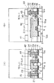
図5はメモリセルの平面図、図6(a)は図5のa−a’線断面図、図6(b)は図5のb−b’線断面図である。なお、平面図においては、絶縁膜、ビット線およびビット線に接続するプラグを省略している。
【0063】
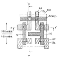
メモリセルを構成する6個のトランジスタは、単結晶シリコンからなる半導体基板上の素子分離5によって周囲を囲まれた活性領域ARに形成されている。nチャネル型の駆動トランジスタD1、D2及び転送トランジスタT1、T2はp型ウェル領域に形成されており、pチャネル型の負荷トランジスタP1、P2はn型ウェル領域に形成されている。
【0064】
一対の転送トランジスタT1、T2のそれぞれは、p型ウェルの活性領域に形成されたn型ソース/ドレイン領域13aと、この活性領域の表面に形成されたゲート酸化膜7と、このゲート酸化膜7上に形成されたゲート電極8で構成されている。このゲート電極8は、例えば、不純物導入多結晶シリコン膜とコバルトシリサイド膜等の高融点金属シリサイド膜の積層構造を有し、ワード線WLと一体に構成されている。ワード線WLは、第1方向(図5中では左右方向)に延在して設けられ、一対の転送トランジスタはこの第1方向に沿って互いに隣接して配置されている。また、一対の転送トランジスタはそのゲート長方向が第1方向と直交する第2方向(図5中では上下方向)と一致するように配置されている。
【0065】
一対の駆動トランジスタD1、D2のそれぞれは、p型ウェルの活性領域に形成されたn型ソース/ドレイン領域13aと、この活性領域の表面に形成されたゲート酸化膜7と、このゲート酸化膜7上に形成されたゲート電極9、10で構成されている。このゲート電極9、10は、例えば、不純物導入多結晶シリコン膜とコバルトシリサイド膜等の高融点金属シリサイド膜の積層構造を有している。
駆動用トランジスタD1のドレイン領域は、転送トランジスタT1のソース/ドレイン領域の一方と共通の活性領域に形成され、駆動用トランジスタD2のドレイン領域は、転送トランジスタT2のソース/ドレイン領域の一方と共通の活性領域に形成されている。
【0066】
一対の負荷トランジスタP1、P2のそれぞれは、n型ウェルの活性領域に形成されたp型ソース/ドレイン領域13bと、この活性領域の表面に形成されたゲート酸化膜7と、このゲート酸化膜7上に形成されたゲート電極9、10で構成されている。負荷トランジスタP1のゲート電極9は駆動トランジスタD1のゲート電極と一体に構成されており、負荷トランジスタP2のゲート電極10は駆動トランジスタD2のゲート電極と一体に構成されている。
【0067】
一対の駆動トランジスタ、一対の負荷トランジスタ及び一対の転送トランジスタのそれぞれのソース/ドレイン領域の表面には、シート抵抗や接続プラグとの接続抵抗を低減する目的でコバルトシリサイド等の高融点金属シリサイド層(不図示)を設けていることが好ましい。
【0068】
一対の駆動トランジスタ、一対の負荷トランジスタ及び一対の転送トランジスタのそれぞれを構成するゲート電極の側壁にはサイドウォール12が形成されている。
【0069】
6個のトランジスタの上部には、シリコン窒化膜14が形成されており、このシリコン窒化膜14の上部には厚さ300〜1000nm程度のPSGやBPSG等からなる第1層間絶縁膜15が形成されている。
【0070】
この第1層間絶縁膜15には、一対のローカル配線の一方である埋込溝配線16(L1)が形成されている。この埋込溝配線16(L1)は、第1層間絶縁膜15を開孔して形成された溝にW等の導電性金属が埋め込まれてなる。この埋込溝配線16(L1)の一端部は、駆動トランジスタD1のドレイン領域と電気的に接続され、他端部は、負荷トランジスタP1のドレイン領域と電気的に接続されている。さらに、埋込溝配線16(L1)の中央部は、駆動トランジスタD2と負荷トランジスタP2に共通のゲート電極10と電気的に接続されている。このゲート電極10は、駆動トランジスタD2のドレイン領域と負荷トランジスタP2のドレイン領域との間でトランジスタD1、P1方向へ分岐し、この分岐した部分が前記埋込溝配線16の中央部と接触している。
【0071】
埋込溝配線16(L1)が形成された第1層間絶縁膜15上には、シリコン酸化膜等からなる厚さ10nm〜150nm程度の第2層間絶縁膜17が形成されている。そして、この第2層間絶縁膜17及び第1層間絶縁膜15に開孔された接続孔にW等の導電性金属が埋め込まれてなる接続プラグが設けられている。これらの接続プラグは、6個のトランジスタのソース/ドレイン領域にそれぞれ接続するプラグ19〜26と、駆動トランジスタD1と負荷トランジスタP1に共通のゲート電極9に接続するプラグ18である。
【0072】
第2層間絶縁膜17の上部には、厚さ100〜200nm程度のTiN等からなるローカル配線27(L2)が形成されている。ローカル配線27(L2)は、駆動トランジスタD1と負荷トランジスタP1に共通のゲート電極9に接続するプラグ18、駆動トランジスタD2のドレイン領域に接続するプラグ19、負荷トランジスタP2のドレイン領域に接続するプラグ20に電気的に接続するように設けられている。また、ローカル配線27(L2)の一部が、他方のローカル配線である前記埋込溝配線16(L1)の上面の少なくとも一部と第2層間絶縁膜17を介して重なるように配置される。ローカル配線27(L2)と埋込溝配線16(L1)とそれらの間に介在する第2層間絶縁膜とで容量素子が構成される。容量素子を設ける点からは、
ローカル配線27(L2)が、埋込溝配線16(L1)の上面をできるだけ覆うことが好ましく、図5に示す構成ではローカル配線27(L2)が、埋込溝配線16(L1)の上面全体を覆っている。
【0073】
なお、接続プラグ21〜26上にはそれぞれ、上層からのビアプラグとの接続を容易にするために、ローカル配線27(L2)と同時にパターニング形成された矩形の導電膜パターン28〜33が形成されている。
【0074】
ローカル配線27(L2)が形成された第2層間絶縁膜17の上部には、シリコン酸化膜等からなる第3層間絶縁膜34が形成され、その上部には、電源電圧Vccが印加される電源電圧線41、及び基準電圧Vssが印加される基準電圧線42が前記第1方向に沿って形成されている。電源電圧線41は、第3層間絶縁膜34に設けられた接続プラグ(ビアプラグ)36、37と第1及び第2層間絶縁膜に設けられた接続プラグ22、23を介して、それぞれ負荷トランジスタP1、P2のソース領域に電気的に接続されている。基準電圧線42は、第3層間絶縁膜34に設けられた接続プラグ(ビアプラグ)35、38と第1及び第2層間絶縁膜に設けられた接続プラグ21、24を介して、それぞれ駆動トランジスタD1、D2のソース領域に電気的に接続されている。これらの配線は、例えば、パターニングされたアルミ膜や、アルミ膜の上部には反射防止膜として下部にはバリアメタル膜としてTiN等からなる膜が配置された積層膜で構成することができる。
【0075】
なお、転送トランジスタT1、T2のソース/ドレイン領域の一方に電気的に接続されるように第3層間絶縁膜34に設けたプラグ39、40の上部にはそれぞれ、上層からのビアプラグとの接続を容易にするために、電源電圧線41及び基準電圧線42と同時にパターニング形成された矩形の導電膜パターン43、44が形成されている。
【0076】
電源電圧線41及び基準電圧線42が形成された第3層間絶縁膜34の上部には、シリコン酸化膜等からなる第4層間絶縁膜(不図示)が形成され、その上部には、前記第2方向に沿って一対のビット線BL1、BL2(不図示)が形成されている。一方のビット線BL1は、第4層間絶縁膜に設けられた接続プラグ(ビアプラグ)と第3層間絶縁膜に設けられた接続プラグ40と第1及び第2層間絶縁膜に設けられた接続プラグ26を介して転送トランジスタT1のソース/ドレイン領域の一方に電気的に接続されている。他方のビット線BL2は、第4層間絶縁膜に設けられた接続プラグ(ビアプラグ)と第3層間絶縁膜に設けられた接続プラグ39と第1及び第2層間絶縁膜並びに第3層間絶縁膜に設けられた接続プラグ25を介して転送トランジスタT2のソース/ドレイン領域の一方に電気的に接続されている。これらの配線は、例えば、パターニングされたアルミ膜や、アルミ膜の上部には反射防止膜として下部にはバリアメタル膜としてTiN等からなる膜が配置された積層膜で構成することができる。
【0077】
次に、本発明の半導体記憶装置のSRAMセルの製造方法を図面を用いて説明する。なお、平面図においては絶縁膜を適宜省略して表記する。
【0078】
まず、p型単結晶シリコンからなる半導体基板1の主面に常法によりシリコン酸化膜2及びシリコン窒化膜3を順次形成する。続いて、常法により形成した所定のパターン形状をもつフォトレジストをマスクにしてドライエッチングを行い、シリコン窒化膜3及びシリコン酸化膜2をパターニングする。その後、残ったシリコン窒化膜3とシリコン酸化膜2をマスクにして半導体基板1をドライエッチングし、素子分離用の溝(トレンチ)4を形成する(図7、図8)。なお、図中、ARで示される領域は活性領域であり、この工程においてはAR以外の領域に素子分離用のトレンチ4が形成される。また、MRで示される点線で囲まれた領域は1つのメモリセル領域を示す。複数のメモリセルは、隣合うメモリセル間で、MRで示される長方形の前記第1方向(図7中では左右方向)に沿う各辺を対象軸としてARの形状が線対称(ミラー反転)になるように配置され、且つ、MRで示される長方形の前記第2方向(図7中では上下方向)に沿う各辺を基準線として前記第1方向に平行移動(シフト)した関係となるように配置される。
なお、MRで示される長方形の各辺を対称軸としてARの形状が線対称になるように基板上に配置することも可能である。
【0079】
次に、図9に示すように、トレンチ4の内部にシリコン酸化膜を埋め込んで素子分離5を形成する。この素子分離5の形成は、トレンチ4を含む半導体基板1上にCVD法によりシリコン酸化膜をトレンチ4内が完全に埋め込まれるように厚く形成した後、シリコン窒化膜3をストッパとして利用し、厚く形成したシリコン酸化膜に対してエッチバックあるいは化学的機械的研磨(CMP)を行いトレンチ4内部以外のシリコン酸化膜を除去して形成することができる。
【0080】
次に、半導体基板1上のシリコン窒化膜3及びシリコン酸化膜2をエッチングにより除去した後、図10及び図11に示すように、厚さ10〜30nm程度の薄いシリコン酸化膜(犠牲酸化膜)2aを形成し、続いて負荷トランジスタP1、P2を形成する領域にレジスト6を形成する。このレジスト6をマスクとし、前記酸化膜2aをスルー膜としてp型不純物(例えばホウ素、BF2)をイオン注入して、駆動トランジスタD1、D2及び転送トランジスタT1、T2を後に設けるp型ウェル領域を形成する。次いで、レジスト6を除去した後、p型ウェル領域上にレジストを形成し、このレジストをマスクとし、前記酸化膜2aをスルー膜としてn型不純物(例えばリン又はヒ素)をイオン注入して、負荷トランジスタP1、P2を後に設けるn型ウェル領域を形成する。
【0081】
次に、半導体基板上のシリコン酸化膜(犠牲酸化膜)2aを除去した後、熱酸化法によりゲート酸化膜を形成し、続いて不純物導入多結晶シリコン膜を形成する。その際、不純物導入多結晶シリコン膜上にWシリサイド膜等の高融点金属シリサイド膜を形成し、その上にキャップ層形成用のシリコン酸化膜を形成してもよい。次いで、所定パターンに形成したフォトレジストをマスクにしてドライエッチングを行い、不純物導入多結晶シリコン膜およびゲート酸化膜を同時にパターニングして、図12及び図13に示すように、転送トランジスタT1、T2のゲート電極(ワード線WL)8、駆動トランジスタD1、D2及び負荷トランジスタP1、P2のゲート電極9、10を形成する。
【0082】
次に、図14及び図15に示すトランジスタ構造を下記のようにして形成する。n型ウェル領域上に形成したレジストをマスクにして、比較的少ない注入量でn型不純物(例えばリン又はヒ素)をイオン注入し、p型ウェル領域にLDD領域11を形成する。このレジストを除去した後、同様に、p型ウェル領域上に形成したレジストをマスクにしてp型不純物(例えばホウ素、BF2)をイオン注入し、n型ウェル領域にLDD領域11を形成する。次いで、このレジストを除去した後、CVD法でシリコン酸化膜を基板上に形成し、このシリコン酸化膜をエッチバックすることにより、ゲート電極の側面にサイドウォール12を形成する。その後、n型ウェル領域上に形成したレジストをマスクにして、比較的多い注入量でn型不純物をイオン注入し、p型ウェル領域にn型ソース/ドレイン領域13aを形成する。続いて、このレジストを除去した後、同様に、p型ウェル領域上に形成したレジストをマスクにしてp型不純物(例えばホウ素、BF2)をイオン注入し、n型ウェル領域にp型ソース/ドレイン領域13bを形成する。
【0083】
この工程後において、好ましくは、ソース/ドレイン領域上に高融点シリサイド膜を形成する。まず、半導体基板上にスパッタリング法等でCo等の高融点金属膜を形成する。次に、熱処理(アニール)を行って、高融点金属膜とソース/ドレイン領域とを反応させた後、未反応の高融点金属をエッチングにより除去する。これによりソース/ドレイン領域上に高融点金属シリサイド膜が形成される。このとき、前述の工程においてゲート電極上にWシリサイド膜およびシリコン酸化膜を設けていない場合は、ゲート電極上にも高融点金属シリサイド膜が形成される。
【0084】
次に、半導体基板上にCVD法でシリコン窒化膜14を形成した後、PSGやBPSG等からなる層間絶縁膜15を形成する。次いで、所定パターンに形成したフォトレジストをマスクにしてドライエッチングを行い第1層間絶縁膜15及びシリコン窒化膜14を開孔して基板表面およびゲート電極に達する溝を形成する。この溝をW等の導電性金属で埋め込むことにより、図16及び図17に示すように、埋込溝配線からなるローカル配線16(L1)を形成する。その際、溝への導電性金属の埋込は、例えば、スパッタリング法等でTi/TiN積層膜等からなるバリア金属膜を溝内部を含む基板上に形成した後、その溝を埋め込むようにW等からなる導電性金属膜をCVD法等により形成し、その後、これら金属膜に対してCMPを行って溝内以外の導電性金属膜とバリア金属膜を除去することにより行うことができる。
【0085】
次に、CVD法によりシリコン酸化膜等からなる第2層間絶縁膜17を形成した後、フォトレジストをマスクにしたドライエッチングを行いゲート電極9に達する接続孔と、ソース/ドレイン領域に達する接続孔(コンタクトホール)を同時に形成する。接続孔内部を含む基板表面に、Ti/TiN積層膜等からなるバリア金属膜を形成した後、CVD法等でこれらの接続孔を埋め込むようにW等の導電性金属膜を形成し、これら金属膜に対してCMPを行って接続孔内以外の導電性金属膜とバリア金属膜を除去する。これにより、ゲート電極9に達する接続プラグ18、ソース/ドレイン領域に達する接続プラグ19〜26が同時に形成される。
【0086】
次に、スパッタリング法またはCVD法等によりTiN膜等の導電膜を形成し、この導電膜をフォトレジストをマスクにしてパターニングを行う。これにより、図20及び図21に示すように、接続プラグ18、19、20に接触するローカル配線(L2)27が形成される。その際、ローカル配線(L2)27は、上面からみて、その一部が第2層間絶縁膜17を介して下層のローカル配線(L1)16の少なくとも一部と重なるように形成される。図においては、ローカル配線(L2)27は、下層のローカル配線(L1)16の上面全体と重なるように形成されている。
【0087】
なお、ローカル配線(L2)27を形成するためのパターニングの際、後に上層に形成される接続プラグ(ビアプラグ)と、各接続プラグ(コンタクトプラグ)21〜26との接続を容易にするために、各接続プラグ21〜26上に、接触し且つその上面を覆う矩形の導電膜パターン28〜33を同時に形成する。
【0088】
次に、CVD法によりシリコン酸化膜等からなる第3の層間絶縁膜34を形成した後、フォトレジストをマスクにしてドライエッチングを行い、各導電膜パターン28〜33に達する接続孔(ビアホール)を形成する。接続孔内部を含む基板表面にバリア金属膜を形成した後、CVD法等でこれらの接続孔を埋め込むようにW等からなる導電性金属膜を形成し、これらの金属膜に対してCMPを行い接続孔以外の導電性金属膜とバリア金属を除去する。これにより、図22及び図23に示すように、各導電膜パターン28〜33に達する接続プラグ(ビアプラグ)が形成される。
【0089】
次に、第3層間絶縁膜34上に、図5及び図6に示すように、電源電圧Vccが印加される電源電圧線41、及び基準電圧Vssが印加される基準電圧線42を形成する。これらの配線は、第3層間絶縁膜34上にスパッタリング法等でAl膜を形成した後、フォトレジストをマスクにしてドライエッチングを行い、Al膜をパターニングして形成することができる。その際、Al膜に代えて、バリアメタル膜(TiN膜等)、Al膜、反射防止膜(TiN膜等)を順次形成してなる積層膜を設けてもよい。電源電圧線41は、接続プラグ36、37に接触し、負荷トランジスタP1、P2のそれぞれのソース領域に電気的に接続される。基準電圧線42は、接続プラグ35、38に接触し、駆動トランジスタD1、D2のそれぞれのソース領域に電気的に接続される。
【0090】
なお、電源電圧線41及び基準電圧線42を形成するためのパターニングの際、転送トランジスタのソース/ドレイン領域の一方に通じる接続プラグ39、40のそれぞれと、後に形成するビット線BL1、BL2に通じる接続プラグとの接続を容易にするために、各接続プラグ39、40上に、それぞれと接接し且つその上面を覆う矩形の導電膜パターン43、44を形成する。
【0091】
次に、電源電圧線41、基準電圧線42等が形成された第3層間絶縁膜34上に、CVD法により酸化シリコン等からなる第4層間絶縁膜を形成する。次いで、フォトレジストをマスクにしたドライエッチングを行って、接続プラグ39、40のそれぞれの上に形成された各導電膜パターン43、44に達する接続孔を形成する。続いて、これらの接続孔の内部を含む第4層間絶縁膜上にバリア金属膜を形成した後、CVD法等によりW等からなる導電性金属膜をこれらの接続孔が埋め込まれるように形成する。次いで、CMPを行って接続孔内部以外のこれら金属膜を除去して接続プラグを形成する。
【0092】
次に、これらの接続プラグが形成された第4層間絶縁膜上に、ビット線BL1、BL2を形成する。これらのビット線は、第4層間絶縁膜上にスパッタリング法等でAl膜を形成した後、フォトレジストをマスクにしてドライエッチングを行い、Al膜をパターニングして形成することができる。その際、Al膜に代えて、バリアメタル膜(TiN膜等)、Al膜、反射防止膜(TiN膜等)を順次形成してなる積層膜を設けてもよい。各ビット線は、第4層間絶縁膜に形成された接続プラグのいずれかに接触し、転送トランジスタT1、T2のいずれかのソース/ドレイン領域の一方に電気的に接続される。
【0093】
以上の工程により、本実施形態のメモリセルが完成する。なお、この後、例えば、ビット線が形成された第4層間絶縁膜上にパッシベーション膜を形成するなど、適宜、所望の工程を実施することができる。
【0094】
【発明の効果】
本発明によれば、リークの発生を抑えながらメモリセル面積を低減する技術を実現でき、スタンバイ電流の低い素子特性に優れた高集積度の半導体記憶装置を提供することができる。
【図面の簡単な説明】
【図1】本発明を適用するSRAMセルの回路図である。
【図2】従来のSRAMセルのレイアウト図である。
【図3】本発明におけるSRAMセルを構成するトランジスタの模式的断面図である。
【図4】本発明のSRAMセルのレイアウト図である。
【図5】本発明の半導体記憶装置のSRAMセルの一実施形態を説明するための平面図である。
【図6】本発明の半導体記憶装置のSRAMセルの一実施形態を説明するための断面図である。
【図7】本発明の半導体記憶装置のSRAMセルの製造方法を説明するための平面図である。
【図8】本発明の半導体記憶装置のSRAMセルの製造方法を説明するための断面図である。
【図9】本発明の半導体記憶装置のSRAMセルの製造方法を説明するための断面図である。
【図10】本発明の半導体記憶装置のSRAMセルの製造方法を説明するための平面図である。
【図11】本発明の半導体記憶装置のSRAMセルの製造方法を説明するための断面図である。
【図12】本発明の半導体記憶装置のSRAMセルの製造方法を説明するための平面図である。
【図13】本発明の半導体記憶装置のSRAMセルの製造方法を説明するための断面図である。
【図14】本発明の半導体記憶装置のSRAMセルの製造方法を説明するための平面図である。
【図15】本発明の半導体記憶装置のSRAMセルの製造方法を説明するための断面図である。
【図16】本発明の半導体記憶装置のSRAMセルの製造方法を説明するための平面図である。
【図17】本発明の半導体記憶装置のSRAMセルの製造方法を説明するための断面図である。
【図18】本発明の半導体記憶装置のSRAMセルの製造方法を説明するための平面図である。
【図19】本発明の半導体記憶装置のSRAMセルの製造方法を説明するための断面図である。
【図20】本発明の半導体記憶装置のSRAMセルの製造方法を説明するための平面図である。
【図21】本発明の半導体記憶装置のSRAMセルの製造方法を説明するための断面図である。
【図22】本発明の半導体記憶装置のSRAMセルの製造方法を説明するための平面図である。
【図23】本発明の半導体記憶装置のSRAMセルの製造方法を説明するための断面図である。
【符号の説明】
T1、T2 転送トランジスタ
D1、D2 駆動トランジスタ
P1、P2 負荷トランジスタ
BL1、BL2 ビット線
WL ワード線
L1、L2 ローカル配線
N1、N2 蓄積ノード
Vcc 電源電圧
Vss 基準電圧
AR 活性領域
MR 一つのメモリセル領域
1 半導体基板
2 シリコン酸化膜
2a シリコン酸化膜(犠牲酸化膜)
3 シリコン窒化膜
4 トレンチ(溝)
5 素子分離
6 レジスト
7 ゲート酸化膜
8 ゲート電極(ワード線WL)
9、10 ゲート電極
11 LDD領域
12 サイドウォール
13 ソース/ドレイン領域
13a n型ソース/ドレイン領域
13b p型ソース/ドレイン領域
14 シリコン窒化膜
15 第1層間絶縁膜
16 ローカル配線(L1)
17 第2層間絶縁膜
18〜26 接続プラグ
27 ローカル配線(L2)
28〜33、43、44 導電膜パターン
34 第3層間絶縁膜
35〜40 接続プラグ(ビアプラグ)
41 電源電圧線
42 基準電圧線
111、113、116 ローカル配線L1に接続されるコンタクト
112、114、115 ローカル配線L2に接続されるコンタクト
117、118 ビット線へのコンタクト
121 電源電圧線へのコンタクト
122 電源電圧線へのコンタクト
123 基準電圧線(グランド線)へのコンタクト
124 基準電圧線(グランド線)へのコンタクト
131、132 ゲート配線
200 半導体基板
201 LDD領域
202 ソース/ドレイン領域
203 ゲート絶縁膜
204 サイドウォール絶縁膜
205 ゲート電極
206 層間絶縁膜
207 コンタクト
207a 埋込導電部
207b バリア膜
210 高融点金属シリサイド層[0001]
BACKGROUND OF THE INVENTION
The present invention relates to a semiconductor device having an SRAM (Static Random Access Memory).
[0002]
[Prior art]
A basic structure of an SRAM cell which is a semiconductor memory element will be described with reference to the drawings.
[0003]
As shown in the circuit diagram of FIG. 1, the SRAM cell includes a flip-flop circuit as an information storage unit and a data line (bit line BL) for writing / reading information. 1 , BL 2 ) And a flip-flop circuit to control a pair of transfer transistors T 1 , T 2 It consists of The flip-flop circuit is composed of, for example, a pair of CMOS inverters, and each CMOS inverter has one drive transistor D. 1 (D 2 ) And one load transistor P 1 (P 2 ).
[0004]
Transfer transistor T 1 (T 2 ) Is one of the source / drain regions of the load transistor P 1 (P 2 ) And driving transistor D 1 (D 2 ), And the other is connected to the bit line BL. 1 (BL 2 )It is connected to the. A pair of transfer transistors T 1 , T 2 These gates constitute part of the word line WL and are connected to each other.
[0005]
Driving transistor D constituting one of the CMOS inverters 1 And load transistor P 1 Of the drive transistor D constituting the other CMOS inverter 2 And load transistor P 2 Drain (storage node N 2 )It is connected to the. Further, the drive transistor D constituting the other CMOS inverter 2 And load transistor P 2 Of the driving transistor D constituting the one CMOS inverter 1 And load transistor P 1 Drain (storage node N 1 )It is connected to the. In this way, between the pair of CMOS inverters, the input / output portion of one CMOS inverter and the gate of the other CMOS inverter are mutually connected as a pair of wirings L called local wiring (local wiring). 1 , L 2 Are cross-coupled (cross-coupled).
[0006]
And the driving transistor D 1 , D 2 A reference voltage (Vss, for example, GND) is supplied to the source region of the load transistor P 1 , P 2 A source voltage (Vcc) is supplied to the source region.
[0007]
FIG. 2 shows a layout diagram of a conventional general SRAM cell corresponding to the circuit diagram of FIG.
[0008]
AR in the figure indicates an active region, and an impurity diffusion region constituting each transistor is formed. In addition, the range indicated by the alternate long and short dash line in the drawing is the range of one memory cell, and each memory cell is adjacently disposed along the longitudinal direction of the word line WL, and is repeatedly disposed in a direction perpendicular to the longitudinal direction.
[0009]
[0010]
The SRAM cell described above has excellent element characteristics such as being resistant to noise and low power consumption during standby. Conventionally, this type of SRAM cell has been selected and laid out in terms of device characteristics so as not to impair the symmetry of the device structure as much as possible (that is, to suppress unbalance).
[0011]
However, such an SRAM requires six transistors in one memory cell, a large number of wirings, and element separation of a p-type MOSFET and an n-type MOSFET in the same cell. There is a problem that the cell area tends to be large.
[0012]
Therefore, in the semiconductor memory device having such an SRAM, improvement of the integration degree is an important issue. Even if the memory cell is slightly reduced, the degree of integration can be greatly improved as a whole highly integrated semiconductor memory device. Therefore, it is important to make the area of the memory cell as small as possible. For this reason, in conjunction with recent advances in manufacturing technology, further reduction in the spacing between wirings and the spacing between wirings and contacts has been achieved along with miniaturization of the processing size and improvement of the layout.
[0013]
[Problems to be solved by the invention]
However, if the distance between the gate electrode of the transistor and the contact on the impurity diffusion region is too small, there arises a problem that leakage occurs. This phenomenon is caused by the load transistor P 1 , P 2 This is conspicuous in the p-type MOSFET constituting the memory cell, and the standby current (standby current) of the memory cell increases due to the occurrence of leakage. Such a phenomenon becomes a problem particularly in a low power type SRAM.
[0014]
Leakage is remarkable when the contact to the source / drain region is in contact with an LDD (Lightly Doped Drain) region, and one factor is that impurities in the LDD region are absorbed on the contact side. Conceivable. Since the LDD region has a lower impurity concentration than the source / drain region which is a high-concentration impurity diffusion layer, the impurity concentration easily changes due to the absorption of impurities, and a desired junction cannot be formed. It is done.
[0015]
In addition, the reason why the leakage is remarkable in the p-type MOSFET is considered that boron used as the p-type impurity is easily absorbed, particularly when a titanium-based metal film is used as the barrier film constituting the contact. It was remarkable. This is probably because a titanium silicide layer is formed at the contact interface between the titanium-based metal film and the silicon substrate due to the influence of heat treatment during manufacturing, and boron is mainly absorbed by the titanium silicide layer.
[0016]
On the other hand, a refractory metal silicide layer is provided on the impurity diffusion region constituting the source / drain region for the purpose of reducing the sheet resistance and the contact resistance with the contact. In Japanese Patent Laid-Open No. 6-177707, in such a configuration, particularly in a configuration in which a titanium silicide layer is formed on an impurity diffusion layer into which boron ions are implanted as impurity ions, boron in the impurity diffusion layer is a titanium silicide layer. The problem that a low-concentration layer is formed by being absorbed in the film is described. In this publication, impurity ion implantation is performed again to supplement the decrease in impurity concentration in the low-concentration layer, thereby suppressing non-ohmic characteristics and increase in parasitic resistance.
[0017]
However, it is difficult to accurately supplement the predicted decrease in the impurity concentration in the LDD region having a low impurity concentration and forming a shallow junction by ion implantation again. Also, when forming such an LDD region, it is difficult to accurately set a high concentration in anticipation of a decrease in impurity concentration. Further, as described in the above publication, the low concentration layer formed by the absorption of impurities is generated in the vicinity of the contact interface, so that the high concentration remains at the junction, and the LDD having such a concentration distribution. When the region is formed, it is difficult to express the original function of the LDD structure, and the device characteristics are deteriorated.
[0018]
SUMMARY OF THE INVENTION An object of the present invention is to provide a highly integrated semiconductor memory device that realizes a technology capable of reducing the area of a memory cell while suppressing the occurrence of leakage and has excellent element characteristics.
[0019]
[Means for Solving the Problems]
The present invention is a gate electrode formed on a first conductivity type well of a semiconductor substrate via a gate insulating film, and a low-concentration second conductivity type impurity diffusion region formed on both sides of the gate electrode, respectively. An LDD structure composed of an LDD region and a source / drain region which is a high-concentration second conductivity type impurity diffusion region, an interlayer insulating film covering the gate electrode and the LDD structure portion, and an opening formed in the interlayer insulating film In a semiconductor device having a contact embedded with a conductive material,
A contact connected to one source / drain region having the same potential as the first conductivity type well is in contact with the LDD region on the source / drain region side, and
The present invention relates to a semiconductor device characterized in that a contact connected to the other source / drain region having a potential different from that of the first conductivity type well is disposed so as not to contact the LDD region on the source / drain region side.
[0020]
According to another aspect of the present invention, there is provided a semiconductor device having an SRAM in which a memory cell is configured by a flip-flop circuit including a pair of drive transistors and a pair of load transistors and a pair of transfer transistors.
The load transistor includes a gate electrode formed on a semiconductor substrate via a gate insulating film, and an LDD region and a high concentration impurity diffusion region, which are low concentration impurity diffusion regions, formed on both sides of the gate electrode, respectively. An LDD structure consisting of source / drain regions,
The distance in the gate length direction between the contact connected to the source region and the gate electrode is smaller than the width of the LDD region in the gate length direction between the gate electrode and the source region, and
The present invention relates to a semiconductor device characterized in that a contact connected to a drain region is disposed so as not to contact an LDD region on the drain region side.
[0021]
According to another aspect of the present invention, there is provided a semiconductor device having an SRAM in which a memory cell is configured by a flip-flop circuit including a pair of drive transistors and a pair of load transistors and a pair of transfer transistors.
The load transistor and the drive transistor include a gate electrode formed on a semiconductor substrate via a gate insulating film, and an LDD region and a high concentration impurity diffusion region formed on both sides of the gate electrode, respectively. Having an LDD structure composed of source / drain regions which are impurity diffusion regions of
The distance in the gate length direction between the contact connected to the source region and the gate electrode is smaller than the width of the LDD region in the gate length direction between the gate electrode and the source region, and
The present invention relates to a semiconductor device characterized in that a contact connected to a drain region is disposed so as not to contact an LDD region on the drain region side.
[0022]
According to the present invention, the transfer transistor includes a gate electrode formed on a semiconductor substrate via a gate insulating film, an LDD region that is a low-concentration impurity diffusion region formed on both sides of the gate electrode, and a high-concentration region. Having an LDD structure composed of source / drain regions which are impurity diffusion regions having a concentration;
The present invention relates to the above semiconductor device in which the contact connected to the source / drain region is arranged so as not to contact the LDD region on the source / drain region side.
[0023]
The present invention also relates to the above semiconductor device in which the contact has at least a bottom portion made of titanium or a titanium-containing material.
[0024]
The present invention also relates to the above semiconductor device, wherein the impurity diffusion region of the load transistor contains boron.
[0025]
The present invention also relates to the above semiconductor device in which a refractory metal silicide layer is formed on the surface of each source / drain region of the load transistor, drive transistor, and transfer transistor.
[0026]
According to the present invention, there is provided a gate electrode in which a contact connected to a drain region of one first load transistor of the pair of load transistors is composed of a first conductive film wiring A common to the gate electrode of the first load transistor. A buried trench wiring formed integrally with a contact connected to the drain region of the first driving transistor having, and provided in the first insulating film which is an interlayer insulating film;
The buried trench wiring constitutes one of a pair of local wirings that cross-couple between a pair of input / output terminals of the flip-flop circuit,
The second conductive film wiring formed by a second conductive film provided on the first insulating film via a second insulating film, wherein the other of the pair of local wirings is configured. The present invention relates to a semiconductor device.
[0027]
According to the present invention, the second conductive film wiring is disposed so as to overlap at least a part of the upper surface of the buried groove wiring with the second insulating film interposed therebetween, and the buried groove wiring and the second conductive film The present invention relates to the above-described semiconductor device in which a capacitive element is constituted by the wiring and the second insulating film interposed therebetween.
[0028]
In the invention, it is preferable that the buried trench wiring includes a drain region of one of the pair of drive transistors and a drain region of the first load transistor of the pair of load transistors. And the first conductive film wiring B constituting the gate electrode of the other second driving transistor and the other second load transistor,
The second conductive film wiring is connected to the first conductive film wiring A constituting the gate electrode of the first driving transistor and the first load transistor, and the contact is connected to the drain region of the second driving transistor. And the semiconductor device in contact with the contact connected to the drain region of the second load transistor.
[0029]
DETAILED DESCRIPTION OF THE INVENTION
One of the main features of the present invention resides in a specific layout structure related to the distance in the gate length direction between the contact connected to the source / drain region and the gate electrode in the MOS field effect transistor (MOSFET) having the LDD structure. . A MOSFET having such a structure is suitable as a transistor constituting a highly integrated semiconductor device such as an SRAM.
[0030]
Hereinafter, an example in which the present invention is applied to an SRAM will be described as a preferred embodiment of the present invention.
[0031]
The SRAM memory cell of this embodiment includes a word line WL and a pair of bit lines BL as shown in FIG. 1 , BL 2 And a pair of drive transistors D 1 , D 2 And a pair of load transistors P 1 , P 2 And a pair of transfer transistors T 1 , T 2 It consists of Here, a pair of drive transistors D 1 , D 2 And a pair of transfer transistors T 1 , T 2 Is an n-channel type, and a pair of load transistors P 1 , P 2 Is configured as a p-channel type.
[0032]
A pair of drive transistors D 1 , D 2 And a pair of load transistors P 1 , P 2 Constitutes a flip-flop circuit as an information storage unit for storing 1-bit information. This flip-flop circuit is composed of a pair of CMOS inverters, and each CMOS inverter has one drive transistor D. 1 (D 2 ) And one load transistor P 1 (P 2 ).
[0033]
Transfer transistor T 1 (T 2 ) Is one of the source / drain regions of the load transistor P 1 (P 2 ) And driving transistor D 1 (D 2 ), And the other is connected to the bit line BL. 1 (BL 2 )It is connected to the. A pair of transfer transistors T 1 , T 2 These gates constitute part of the word line WL and are connected to each other.
[0034]
Driving transistor D constituting one of the CMOS inverters 1 And load transistor P 1 Of the drive transistor D constituting the other CMOS inverter 2 And load transistor P 2 Drain (storage node N 2 )It is connected to the. Further, the drive transistor D constituting the other CMOS inverter 2 And load transistor P 2 Of the driving transistor D constituting the one CMOS inverter 1 And load transistor P 1 Drain (storage node N 1 )It is connected to the. In this way, between the pair of CMOS inverters, the input / output part (storage node) of one CMOS inverter and the gate of the other CMOS inverter are mutually connected as a pair of wirings L called local wiring (local wiring). 1 , L 2 Are cross-coupled (cross-coupled).
[0035]
And the driving transistor D 1 , D 2 A reference voltage (Vss, for example, GND) is supplied to the source region of the load transistor P 1 , P 2 A source voltage (Vcc) is supplied to the source region.
[0036]
Next, an embodiment of a specific layout structure related to the distance in the gate length direction between the contact connected to the source / drain region and the gate electrode in the MOSFET having the LDD structure will be described with reference to FIGS.
[0037]
FIG. 3 shows a schematic cross-sectional structure of the drive transistor and load transistor constituting the SRAM cell of this embodiment, and FIG. 4 shows a layout diagram of the SRAM cell. In FIG. 4, the same reference numerals are used for the same portions as in FIG.
[0038]
A
[0039]
In addition, an
[0040]
The gate length of the
[0041]
In the MOSFET, a refractory
[0042]
The above MOSFET can be manufactured as follows, for example.
[0043]
First, an element isolation insulating film is formed on a silicon semiconductor substrate by a trench isolation method, and a gate insulating film and a gate electrode are formed on an active region where the element isolation insulating film is not formed.
[0044]
Next, low dose impurity ion implantation is performed to form a low-concentration impurity layer, and then an insulating film is formed and then etched back to form sidewall insulating films on both sides of the gate electrode. Next, after a high dose impurity layer is formed by implanting high dose impurity ions, the low concentration impurity layer and the high concentration impurity layer are activated by heat treatment to form LDD regions and source / drain regions.
[0045]
Next, a refractory metal film such as Co is formed on the silicon semiconductor substrate by sputtering, and then heat treatment is performed to cause the refractory metal film to react with silicon, and a high melting point is formed on the gate electrode and source / drain regions. A metal silicide film is formed. Unreacted refractory metal film is removed by wet etching.
[0046]
As shown in FIG. 3, an
It is also possible to form a contact by filling the contact hole with a titanium-containing material.
[0047]
One important configuration of the semiconductor device according to the present invention is that a contact connected to one source / drain region that is not equipotential to the first conductivity type well does not contact an LDD region on the source / drain region side. It is arranged. With such an arrangement, it is possible to prevent deterioration in element characteristics such as leakage due to contact between the contact and the LDD region. For the contact connected to the first conductivity type well and the other source / drain region having the same potential, the distance between the contact and the gate electrode in the gate length direction is the gate length between the gate electrode and the source / drain region. It arrange | positions so that it may become smaller than the LDD area | region width of a direction. With such an arrangement, even if the contact is in contact with the LDD region, the device characteristics such as leakage are hardly deteriorated, and the distance between the contact and the gate electrode can be narrowed. It becomes possible to improve.
[0048]
In the SRAM cell of this embodiment, the load transistor P 1 , P 2 As shown in FIG. 3, the p-type MOSFET having the LDD structure is arranged so that the contact connected to the drain region does not contact the LDD region on the drain region side. That is, the distance W1 (corresponding to B1 and B2 in FIG. 4) between the contact connected to the drain region and the gate electrode in the gate length direction is made larger than the LDD region width W3 in the gate length direction between the gate electrode and the drain region. . Furthermore, it is preferable to provide the contact on the silicide region so as not to directly contact the impurity diffusion region.
By disposing the contacts so as not to contact the LDD region in this manner, boron suction in the LDD region can be suppressed, and as a result, occurrence of leakage can be prevented. This interval W1 (B1, B2) can be appropriately set as long as the contact does not contact the LDD region, but is preferably set to 0.08 μm or more so that the memory size does not become too large. Currently, it can be set to about 0.16 μm in consideration of the capacity of mass production equipment.
[0049]
On the other hand, the load transistor P 1 , P 2 , The distance W2 (corresponding to A1 and A2 in FIG. 4) between the contact connected to the source region and the gate electrode in the gate length direction is made smaller than the LDD region width W4 in the gate length direction between the gate electrode and the source region. . In this case, even if the contact is in contact with the LDD region, no bias is applied to the junction of the impurity diffusion region on the source region side, so that leakage occurs even if the impurity concentration in the LDD region on the source region side slightly changes due to boron absorption. do not do. This interval W2 (A1, A2) is preferably 0.01 μm or more from the viewpoint of ensuring sufficient insulation, and can be set to about 0.13 μm as a size that does not make the memory size too large.
[0050]
In addition, a driving transistor D composed of an n-type MOSFET having an LDD structure 1 , D 2 However, as in the load transistor, it is preferable to arrange the contact connected to the drain region so as not to contact the LDD region on the drain region side. That is, the distance W1 (corresponding to F1 and F2 in FIG. 4) between the contact connected to the drain region and the gate electrode in the gate length direction is made larger than the LDD region width W3 in the gate length direction between the gate electrode and the drain region. It is desirable. Furthermore, it is preferable to provide the contact on the silicide region so as not to directly contact the impurity diffusion region. By arranging the contacts so as not to contact the LDD region in this way, it is possible to prevent the contact from affecting the element characteristics. This interval W1 (F1, F2) can be set as appropriate if the contact does not contact the LDD region, but is preferably set to 0.06 μm or more, and is set to a size that prevents the memory size from becoming too large. It can be set to about 16 μm.
[0051]
On the other hand, the driving transistor D 1 , D 2 , The distance W2 (corresponding to E1 and E2 in FIG. 4) between the connection contact and the gate electrode in the source region is made smaller than the LDD region width W4 in the gate length direction between the gate electrode and the source region. Is preferred. In this case, even if the contact is in contact with the LDD region, since the bias is not applied to the junction of the impurity diffusion region on the source region side, it is difficult to be affected by the element characteristics due to this contact. This interval W2 (E1, E2) is preferably 0.01 μm or more from the viewpoint of ensuring sufficient insulation, and can be set to about 0.13 μm as a size that does not make the memory size too large.
[0052]
The setting of the interval W2 in FIG. 3 in the load transistor and the drive transistor is to narrow the intervals A1, A2, E1, and E2 in FIG. 4, and the memory cell width in the longitudinal direction of the word line can be reduced.
[0053]
In the SRAM cell of this embodiment, the transfer transistor T 1 , T 2 It is preferable to arrange the contacts connected to the source / drain regions so as not to contact the LDD regions on the source / drain regions side. In this case, the distance in the gate length direction between the contact connected to the source / drain region on the outer peripheral side of the memory cell and the gate electrode (corresponding to G1 and G2 in FIG. 4) is the gate between the gate electrode and the source / drain region. The arrangement is larger than the width of the LDD region in the long direction. Furthermore, it is preferable to provide the contact on the silicide region so as not to directly contact the impurity diffusion region. The distances G1 and G2 are preferably 0.06 μm or more from the viewpoint of ensuring sufficient insulation, and can be set to about 0.13 μm as a size that does not cause the memory size to become too large. Note that the contact connected to the other source / drain region (the contact common to the contact connected to the drain region of the driving transistor) is preferably not in contact with the LDD region on the source / drain region side.
[0054]
In the configuration described above, the inventor has found that the distance between the contact and the gate electrode is smaller than the LDD region in the impurity diffusion region having the same potential as the well potential, and in the impurity diffusion region having a potential different from the well potential. It is preferable to make it larger than the LDD region. In particular, for the p-type MOSFET, it has been found that the impurity diffusion region having a potential different from the well potential is larger than the LDD region and that the contact is preferably provided on the silicide region. Is.
[0055]
As described above, it is possible to suppress the deterioration of element characteristics such as the occurrence of leaks and to reduce the memory cell. Further, a specific layout structure related to the distance between the contact on the source / drain region and the gate electrode is provided. When applied to the structure shown in FIGS. 5 and 6, the memory cell can be further reduced.
[0056]
In the embodiment shown in FIGS. 5 and 6, a pair of local wires L 1 , L 2 Are arranged in different layers, the local wiring in the lower layer is constituted by buried trench wiring, the local wiring in the upper layer is constituted by a plate-like conductive film, and the upper local wiring (plate-like) is viewed from the upper surface (plane) of the substrate. A part of the wiring) is arranged so as to overlap at least part of the upper surface of the lower local wiring (buried groove wiring) with an insulating film interposed therebetween.
[0057]
The buried trench wiring constituting one of the local wirings is connected to the load transistor P 1 Contact on the drain region and the drive transistor D 1 And the contact on the drain region are integrally formed. In the SRAM cell of this embodiment, the buried trench wiring is connected to the load transistor P. 1 And driving transistor D 1 In either case, the electrodes are arranged so as not to contact the LDD region on the drain region side. That is, at least on the active region, the interval between the buried trench wiring and the gate electrode is set larger than the width of the LDD region in the gate length direction between the gate electrode and the drain region.
[0058]
Other layout structures relating to the distance between the contact on the source / drain region and the gate electrode can be set in the same manner as in the above-described embodiment. However, in the structure shown in FIG. 1 , P 2 Each of the
[0059]
In the above structure, in addition to preventing leakage and further reducing the memory cell area, the lower layer local wiring (buried groove wiring) and the upper layer local wiring (plate-shaped wiring) and the insulation interposed therebetween Since the capacitive element is composed of the film, it is possible to prevent the α-ray soft error resistance from being lowered due to the miniaturization of the memory cell size and the reduction of the operating voltage.
[0060]
In addition, according to this structure, one of the local wirings provided in the lower layer is formed of the buried trench wiring, so that the connection plug can be formed simultaneously with the formation of the local wiring in the lower layer. can do.
[0061]
A specific structure of the SRAM cell will be further described with reference to the drawings.
[0062]
5 is a plan view of the memory cell, FIG. 6A is a cross-sectional view taken along the line aa ′ in FIG. 5, and FIG. 6B is a cross-sectional view taken along the line bb ′ in FIG. In the plan view, the insulating film, the bit line, and the plug connected to the bit line are omitted.
[0063]
Six transistors constituting the memory cell are formed in an active region AR surrounded by
[0064]
A pair of transfer transistors T 1 , T 2 Are each an n-type source /
[0065]
A pair of drive transistors D 1 , D 2 Are each an n-type source /
Driving transistor D 1 The drain region of the transfer transistor T 1 Drive transistor D formed in an active region common to one of the source / drain regions of 2 The drain region of the transfer transistor T 2 Are formed in an active region common to one of the source / drain regions.
[0066]
A pair of load transistors P 1 , P 2 Each includes a p-type source /
[0067]
A refractory metal silicide layer (such as cobalt silicide) is formed on the surfaces of the source / drain regions of the pair of drive transistors, the pair of load transistors, and the pair of transfer transistors in order to reduce the sheet resistance and the connection resistance with the connection plug. (Not shown) is preferably provided.
[0068]
[0069]
A
[0070]
The first
[0071]
Embedded trench wiring 16 (L 1 A second
[0072]
On top of the second
Local wiring 27 (L 2 ) Is buried trench wiring 16 (L 1 ) Is preferably covered as much as possible. In the configuration shown in FIG. 5, the local wiring 27 (L 2 ) Is buried trench wiring 16 (L 1 ) Covering the entire top surface.
[0073]
It should be noted that the local wiring 27 (L 2 At the same time, rectangular
[0074]
Local wiring 27 (L 2 The third
[0075]
The transfer transistor T 1 , T 2 In order to facilitate the connection with the via plug from the upper layer, the upper portion of the
[0076]
A fourth interlayer insulating film (not shown) made of a silicon oxide film or the like is formed on the third
[0077]
Next, a method for manufacturing the SRAM cell of the semiconductor memory device of the present invention will be described with reference to the drawings. In the plan view, the insulating film is omitted as appropriate.
[0078]
First, the
In addition, it is also possible to arrange on the substrate so that the shape of the AR is axisymmetric with respect to each side of the rectangle indicated by MR.
[0079]
Next, as shown in FIG. 9, the
[0080]
Next, after removing the
[0081]
Next, after removing the silicon oxide film (sacrificial oxide film) 2a on the semiconductor substrate, a gate oxide film is formed by a thermal oxidation method, and then an impurity-introduced polycrystalline silicon film is formed. At this time, a refractory metal silicide film such as a W silicide film may be formed on the impurity-doped polycrystalline silicon film, and a silicon oxide film for forming a cap layer may be formed thereon. Next, dry etching is performed using the photoresist formed in a predetermined pattern as a mask, and the impurity-introduced polycrystalline silicon film and the gate oxide film are patterned at the same time, and as shown in FIGS. 12 and 13, the transfer transistor T 1 , T 2 Gate electrode (word line WL) 8 and drive transistor D 1 , D 2 And load transistor P 1 , P 2 The
[0082]
Next, the transistor structure shown in FIGS. 14 and 15 is formed as follows. Using a resist formed on the n-type well region as a mask, n-type impurities (for example, phosphorus or arsenic) are ion-implanted with a relatively small implantation amount to form the
[0083]
After this step, a refractory silicide film is preferably formed on the source / drain regions. First, a refractory metal film such as Co is formed on a semiconductor substrate by sputtering or the like. Next, heat treatment (annealing) is performed to react the refractory metal film with the source / drain regions, and then the unreacted refractory metal is removed by etching. As a result, a refractory metal silicide film is formed on the source / drain regions. At this time, if the W silicide film and the silicon oxide film are not provided on the gate electrode in the above process, a refractory metal silicide film is also formed on the gate electrode.
[0084]
Next, after a
[0085]
Next, after a second
[0086]
Next, a conductive film such as a TiN film is formed by sputtering or CVD, and patterning is performed using the conductive film as a mask for the conductive film. Thereby, as shown in FIGS. 20 and 21, the local wiring (L 2 27) is formed. At that time, local wiring (L 2 ) 27 is a part of the local wiring (L) in the lower layer through the second
[0087]
Note that local wiring (L 2 In order to facilitate the connection between the connection plugs (via plugs) formed later in the upper layer and the connection plugs (contact plugs) 21 to 26 at the time of patterning for forming 27), the connection plugs 21 to 26 are formed. On the top, rectangular
[0088]
Next, after a third
[0089]
Next, as shown in FIGS. 5 and 6, the power
[0090]
In the patterning for forming the power
[0091]
Next, a fourth interlayer insulating film made of silicon oxide or the like is formed by CVD on the third
[0092]
Next, the bit line BL is formed on the fourth interlayer insulating film in which these connection plugs are formed. 1 , BL 2 Form. These bit lines can be formed by forming an Al film on the fourth interlayer insulating film by sputtering or the like, then performing dry etching using a photoresist as a mask, and patterning the Al film. At that time, instead of the Al film, a laminated film formed by sequentially forming a barrier metal film (TiN film or the like), an Al film, and an antireflection film (TiN film or the like) may be provided. Each bit line contacts one of the connection plugs formed in the fourth interlayer insulating film, and the transfer transistor T 1 , T 2 Are electrically connected to one of the source / drain regions.
[0093]
Through the above steps, the memory cell of this embodiment is completed. Thereafter, a desired process can be appropriately performed, for example, forming a passivation film on the fourth interlayer insulating film in which the bit line is formed.
[0094]
【The invention's effect】
According to the present invention, a technology for reducing the memory cell area while suppressing the occurrence of leakage can be realized, and a highly integrated semiconductor memory device excellent in element characteristics with a low standby current can be provided.
[Brief description of the drawings]
FIG. 1 is a circuit diagram of an SRAM cell to which the present invention is applied.
FIG. 2 is a layout diagram of a conventional SRAM cell.
FIG. 3 is a schematic cross-sectional view of a transistor constituting an SRAM cell in the present invention.
FIG. 4 is a layout diagram of the SRAM cell of the present invention.
FIG. 5 is a plan view for explaining one embodiment of an SRAM cell of the semiconductor memory device of the present invention.
FIG. 6 is a cross-sectional view for explaining an embodiment of an SRAM cell of the semiconductor memory device of the present invention.
FIG. 7 is a plan view illustrating the method for manufacturing the SRAM cell of the semiconductor memory device of the present invention.
FIG. 8 is a cross-sectional view for explaining the method of manufacturing the SRAM cell of the semiconductor memory device of the present invention.
FIG. 9 is a cross-sectional view for explaining the method of manufacturing the SRAM cell of the semiconductor memory device of the present invention.
FIG. 10 is a plan view illustrating the method for manufacturing the SRAM cell of the semiconductor memory device of the present invention.
FIG. 11 is a cross-sectional view for explaining the method of manufacturing the SRAM cell of the semiconductor memory device of the present invention.
FIG. 12 is a plan view for illustrating the method for manufacturing the SRAM cell of the semiconductor memory device of the present invention.
FIG. 13 is a cross-sectional view for illustrating the method for manufacturing the SRAM cell of the semiconductor memory device of the present invention.
FIG. 14 is a plan view for explaining the method for manufacturing the SRAM cell of the semiconductor memory device of the present invention.
FIG. 15 is a cross-sectional view for illustrating the method of manufacturing the SRAM cell of the semiconductor memory device of the present invention.
FIG. 16 is a plan view for illustrating the method for manufacturing the SRAM cell of the semiconductor memory device of the present invention.
FIG. 17 is a cross-sectional view for illustrating the method of manufacturing the SRAM cell of the semiconductor memory device of the present invention.
FIG. 18 is a plan view illustrating the method for manufacturing the SRAM cell of the semiconductor memory device of the present invention.
FIG. 19 is a cross sectional view for illustrating the method for manufacturing the SRAM cell of the semiconductor memory device of the present invention.
FIG. 20 is a plan view for explaining the method for manufacturing the SRAM cell of the semiconductor memory device of the present invention.
FIG. 21 is a cross-sectional view for illustrating the method of manufacturing the SRAM cell of the semiconductor memory device of the present invention.
FIG. 22 is a plan view for explaining the method for manufacturing the SRAM cell of the semiconductor memory device of the present invention.
FIG. 23 is a cross-sectional view for illustrating the method of manufacturing the SRAM cell of the semiconductor memory device of the present invention.
[Explanation of symbols]
T 1 , T 2 Transfer transistor
D 1 , D 2 Driving transistor
P 1 , P 2 Load transistor
BL 1 , BL 2 Bit line
WL Word line
L 1 , L 2 Local wiring
N 1 , N 2 Accumulation node
Vcc supply voltage
Vss reference voltage
AR active region
MR One memory cell area
1 Semiconductor substrate
2 Silicon oxide film
2a Silicon oxide film (sacrificial oxide film)
3 Silicon nitride film
4 Trench
5 element isolation
6 resists
7 Gate oxide film
8 Gate electrode (word line WL)
9, 10 Gate electrode
11 LDD region
12 Sidewall
13 Source / drain region
13a n-type source / drain region
13b p-type source / drain region
14 Silicon nitride film
15 First interlayer insulating film
16 Local wiring (L 1 )
17 Second interlayer insulating film
18-26 connection plug
27 Local wiring (L 2 )
28-33, 43, 44 Conductive film pattern
34 Third interlayer insulating film
35-40 Connection plug (via plug)
41 Power supply voltage line
42 Reference voltage line
111, 113, 116 Local wiring L 1 Contact connected to
112, 114, 115 Local wiring L 2 Contact connected to
117, 118 Contact to bit line
121 Contact to the power supply voltage line
122 Contact to the power supply voltage line
123 Contact to the reference voltage line (ground line)
124 Contact to the reference voltage line (ground line)
131, 132 Gate wiring
200 Semiconductor substrate
201 LDD region
202 Source / drain region
203 Gate insulation film
204 Side wall insulating film
205 Gate electrode
206 Interlayer insulation film
207 contacts
207a Buried conductive part
207b Barrier film
210 Refractory metal silicide layer
Claims (9)
前記負荷トランジスタ及び前記駆動トランジスタは、半導体基板上にゲート絶縁膜を介して形成されたゲート電極と、前記ゲート電極の両側にそれぞれ形成された、低濃度の不純物拡散領域であるLDD領域および高濃度の不純物拡散領域であるソース/ドレイン領域からなるLDD構造を有し、
ソース領域に接続するコンタクトとゲート電極とのゲート長方向の間隔が、ゲート電極とソース領域間のゲート長方向のLDD領域幅より小さく、且つドレイン領域に接続するコンタクトがドレイン領域側のLDD領域に接しないように配置され、
前記一対の負荷トランジスタの一方の第1負荷トランジスタのドレイン領域に接続するコンタクトは、この第1負荷トランジスタのゲート電極と共通の第1導電膜配線Aで構成されるゲート電極を持つ第1駆動トランジスタのドレイン領域に接続するコンタクトと一体に形成され、層間絶縁膜である第1絶縁膜に設けられた埋込溝配線であり、
前記埋込溝配線は、前記フリップフロップ回路の一対の入出力端子間を交差結合する一対のローカル配線の一方を構成し、
前記第1絶縁膜上に第2絶縁膜を介して設けられた第2導電膜で形成された第2導電膜配線で、前記一対のローカル配線の他方が構成されていることを特徴とする半導体装置。In a semiconductor device having an SRAM that forms a memory cell with a flip-flop circuit composed of a pair of drive transistors and a pair of load transistors and a pair of transfer transistors,
The load transistor and the drive transistor include a gate electrode formed on a semiconductor substrate via a gate insulating film, and an LDD region and a high concentration impurity diffusion region formed on both sides of the gate electrode, respectively. Having an LDD structure composed of source / drain regions which are impurity diffusion regions of
The distance in the gate length direction between the contact connected to the source region and the gate electrode is smaller than the width of the LDD region in the gate length direction between the gate electrode and the source region, and the contact connected to the drain region is in the LDD region on the drain region side. Arranged so as not to touch ,
A first drive transistor having a gate electrode formed of a first conductive film wiring A common to the gate electrode of the first load transistor, the contact connected to the drain region of the first load transistor of the pair of load transistors A buried trench wiring formed integrally with a contact connected to the drain region of the first insulating film, which is an interlayer insulating film,
The buried trench wiring constitutes one of a pair of local wirings that cross-couple between a pair of input / output terminals of the flip-flop circuit,
A second conductive film wiring formed by a second conductive film provided on the first insulating film via a second insulating film, wherein the other of the pair of local wirings is configured. apparatus.
ソース/ドレイン領域に接続するコンタクトが、そのソース/ドレイン領域側のLDD領域に接しないように配置されている請求項1に記載の半導体装置。The transfer transistor includes a gate electrode formed on a semiconductor substrate through a gate insulating film, an LDD region that is a low concentration impurity diffusion region, and a high concentration impurity diffusion region formed on both sides of the gate electrode, respectively. An LDD structure consisting of source / drain regions,
The semiconductor device according to claim 1 , wherein the contact connected to the source / drain region is arranged so as not to contact the LDD region on the source / drain region side.
前記第2導電膜配線は、前記第1駆動トランジスタ及び前記第1負荷トランジスタのゲート電極を構成する前記第1導電膜配線Aに接続するコンタクトと、前記第2駆動トランジスタのドレイン領域に接続するコンタクトと、前記第2負荷トランジスタのドレイン領域に接続するコンタクトとに接している請求項1から8のいずれか一項に記載の半導体装置。The buried trench wiring includes a drain region of one of the first drive transistors of the pair of drive transistors, a drain region of the first load transistor of the pair of load transistors, and the other of the first drive transistors. Arranged so as to be connected to the first conductive film wiring B constituting the gate electrode of the two drive transistors and the other second load transistor,
The second conductive film wiring includes a contact connected to the first conductive film wiring A constituting a gate electrode of the first drive transistor and the first load transistor, and a contact connected to a drain region of the second drive transistor. The semiconductor device according to claim 1, which is in contact with a contact connected to a drain region of the second load transistor.
Priority Applications (4)
| Application Number | Priority Date | Filing Date | Title |
|---|---|---|---|
| JP2001131542A JP4570811B2 (en) | 2001-04-27 | 2001-04-27 | Semiconductor device |
| TW091107725A TW543087B (en) | 2001-04-27 | 2002-04-16 | Semiconductor device |
| US10/131,206 US6765272B2 (en) | 2001-04-27 | 2002-04-25 | Semiconductor device |
| KR1020020023240A KR20020083513A (en) | 2001-04-27 | 2002-04-27 | Semiconductor device |
Applications Claiming Priority (1)
| Application Number | Priority Date | Filing Date | Title |
|---|---|---|---|
| JP2001131542A JP4570811B2 (en) | 2001-04-27 | 2001-04-27 | Semiconductor device |
Publications (2)
| Publication Number | Publication Date |
|---|---|
| JP2002329798A JP2002329798A (en) | 2002-11-15 |
| JP4570811B2 true JP4570811B2 (en) | 2010-10-27 |
Family
ID=18979710
Family Applications (1)
| Application Number | Title | Priority Date | Filing Date |
|---|---|---|---|
| JP2001131542A Expired - Fee Related JP4570811B2 (en) | 2001-04-27 | 2001-04-27 | Semiconductor device |
Country Status (4)
| Country | Link |
|---|---|
| US (1) | US6765272B2 (en) |
| JP (1) | JP4570811B2 (en) |
| KR (1) | KR20020083513A (en) |
| TW (1) | TW543087B (en) |
Families Citing this family (34)
| Publication number | Priority date | Publication date | Assignee | Title |
|---|---|---|---|---|
| US6897477B2 (en) * | 2001-06-01 | 2005-05-24 | Semiconductor Energy Laboratory Co., Ltd. | Semiconductor device, manufacturing method thereof, and display device |
| KR100421048B1 (en) * | 2001-09-07 | 2004-03-04 | 삼성전자주식회사 | Semiconductor device having local interconnection layer & fabricating method thereof |
| JP2005072185A (en) * | 2003-08-22 | 2005-03-17 | Fujitsu Ltd | Semiconductor device and manufacturing method thereof |
| US8212317B2 (en) | 2004-01-29 | 2012-07-03 | Enpirion, Inc. | Integrated circuit with a laterally diffused metal oxide semiconductor device and method of forming the same |
| US8253196B2 (en) | 2004-01-29 | 2012-08-28 | Enpirion, Inc. | Integrated circuit with a laterally diffused metal oxide semiconductor device and method of forming the same |
| US8253197B2 (en) * | 2004-01-29 | 2012-08-28 | Enpirion, Inc. | Integrated circuit with a laterally diffused metal oxide semiconductor device and method of forming the same |
| US7230302B2 (en) * | 2004-01-29 | 2007-06-12 | Enpirion, Inc. | Laterally diffused metal oxide semiconductor device and method of forming the same |
| US8212316B2 (en) * | 2004-01-29 | 2012-07-03 | Enpirion, Inc. | Integrated circuit with a laterally diffused metal oxide semiconductor device and method of forming the same |
| US8253195B2 (en) * | 2004-01-29 | 2012-08-28 | Enpirion, Inc. | Integrated circuit with a laterally diffused metal oxide semiconductor device and method of forming the same |
| US8212315B2 (en) | 2004-01-29 | 2012-07-03 | Enpirion, Inc. | Integrated circuit with a laterally diffused metal oxide semiconductor device and method of forming the same |
| US20050275043A1 (en) * | 2004-06-10 | 2005-12-15 | Chien-Chao Huang | Novel semiconductor device design |
| KR101039471B1 (en) * | 2004-06-11 | 2011-06-07 | 엘지디스플레이 주식회사 | Array substrate for liquid crystal display device and manufacturing method thereof |
| US7190026B2 (en) * | 2004-08-23 | 2007-03-13 | Enpirion, Inc. | Integrated circuit employable with a power converter |
| US7186606B2 (en) * | 2004-08-23 | 2007-03-06 | Enpirion, Inc. | Method of forming an integrated circuit employable with a power converter |
| US7214985B2 (en) * | 2004-08-23 | 2007-05-08 | Enpirion, Inc. | Integrated circuit incorporating higher voltage devices and low voltage devices therein |
| US7229886B2 (en) * | 2004-08-23 | 2007-06-12 | Enpirion, Inc. | Method of forming an integrated circuit incorporating higher voltage devices and low voltage devices therein |
| US7335948B2 (en) * | 2004-08-23 | 2008-02-26 | Enpirion, Inc. | Integrated circuit incorporating higher voltage devices and low voltage devices therein |
| US7232733B2 (en) * | 2004-08-23 | 2007-06-19 | Enpirion, Inc. | Method of forming an integrated circuit incorporating higher voltage devices and low voltage devices therein |
| US7195981B2 (en) | 2004-08-23 | 2007-03-27 | Enpirion, Inc. | Method of forming an integrated circuit employable with a power converter |
| KR100704784B1 (en) * | 2005-03-07 | 2007-04-10 | 삼성전자주식회사 | Stacked semiconductor device and manufacturing method thereof |
| JP5090671B2 (en) * | 2005-08-01 | 2012-12-05 | ルネサスエレクトロニクス株式会社 | Semiconductor device |
| KR100760910B1 (en) * | 2005-12-29 | 2007-09-21 | 동부일렉트로닉스 주식회사 | SRAM Memory Devices with Common Contacts |
| JP2008147340A (en) * | 2006-12-08 | 2008-06-26 | Nec Electronics Corp | Semiconductor device, method for manufacturing semiconductor device, and SRAM cell |
| JP5109403B2 (en) | 2007-02-22 | 2012-12-26 | 富士通セミコンダクター株式会社 | Semiconductor memory device and manufacturing method thereof |
| KR100919215B1 (en) * | 2007-09-06 | 2009-09-28 | 세메스 주식회사 | End effector and robot arm apparatus having the same |
| JP2011018692A (en) * | 2009-07-07 | 2011-01-27 | Fujitsu Semiconductor Ltd | Semiconductor device and method of manufacturing the same |
| US9299691B2 (en) | 2012-11-30 | 2016-03-29 | Enpirion, Inc. | Semiconductor device including alternating source and drain regions, and respective source and drain metallic strips |
| US9536938B1 (en) | 2013-11-27 | 2017-01-03 | Altera Corporation | Semiconductor device including a resistor metallic layer and method of forming the same |
| US9673192B1 (en) | 2013-11-27 | 2017-06-06 | Altera Corporation | Semiconductor device including a resistor metallic layer and method of forming the same |
| US10020739B2 (en) | 2014-03-27 | 2018-07-10 | Altera Corporation | Integrated current replicator and method of operating the same |
| US10103627B2 (en) | 2015-02-26 | 2018-10-16 | Altera Corporation | Packaged integrated circuit including a switch-mode regulator and method of forming the same |
| US9484431B1 (en) * | 2015-07-29 | 2016-11-01 | International Business Machines Corporation | Pure boron for silicide contact |
| JP7097952B2 (en) * | 2017-08-29 | 2022-07-08 | マイクロン テクノロジー,インク. | Devices and systems with string drivers including high bandgap materials, and methods of formation |
| JP2021141185A (en) | 2020-03-05 | 2021-09-16 | キオクシア株式会社 | Semiconductor storage device |
Family Cites Families (20)
| Publication number | Priority date | Publication date | Assignee | Title |
|---|---|---|---|---|
| JP2927463B2 (en) * | 1989-09-28 | 1999-07-28 | 株式会社日立製作所 | Semiconductor storage device |
| JP3057268B2 (en) * | 1991-06-27 | 2000-06-26 | ソニー株式会社 | Semiconductor memory device and manufacturing method thereof |
| JP3058956B2 (en) | 1991-09-30 | 2000-07-04 | 株式会社東芝 | Semiconductor device and manufacturing method thereof |
| KR940009608B1 (en) * | 1991-11-30 | 1994-10-15 | 삼성전자 주식회사 | Semiconductor memory device & manufacturing method thereof |
| GB9219268D0 (en) * | 1992-09-11 | 1992-10-28 | Inmos Ltd | Semiconductor device incorporating a contact and manufacture thereof |
| JPH06177067A (en) | 1992-12-04 | 1994-06-24 | Nec Corp | Manufacture of semiconductor integrated circuit device |
| JP2684979B2 (en) * | 1993-12-22 | 1997-12-03 | 日本電気株式会社 | Semiconductor integrated circuit device and method of manufacturing the same |
| US5612552A (en) * | 1994-03-31 | 1997-03-18 | Lsi Logic Corporation | Multilevel gate array integrated circuit structure with perpendicular access to all active device regions |
| US5670395A (en) * | 1996-04-29 | 1997-09-23 | Chartered Semiconductor Manufacturing Pte. Ltd. | Process for self-aligned twin wells without N-well and P-well height difference |
| JPH10163344A (en) * | 1996-12-05 | 1998-06-19 | Hitachi Ltd | Semiconductor integrated circuit device and method of manufacturing the same |
| US5804477A (en) * | 1997-02-24 | 1998-09-08 | Integrated Device Technology, Inc. | Method of making a 6-transistor compact static ram cell |
| JP3807836B2 (en) * | 1997-11-28 | 2006-08-09 | 株式会社ルネサステクノロジ | Semiconductor device and manufacturing method of semiconductor device |
| US6271542B1 (en) * | 1997-12-08 | 2001-08-07 | International Business Machines Corporation | Merged logic and memory combining thin film and bulk Si transistors |
| US6184073B1 (en) * | 1997-12-23 | 2001-02-06 | Motorola, Inc. | Process for forming a semiconductor device having an interconnect or conductive film electrically insulated from a conductive member or region |
| JP3467416B2 (en) | 1998-04-20 | 2003-11-17 | Necエレクトロニクス株式会社 | Semiconductor memory device and method of manufacturing the same |
| US6239491B1 (en) * | 1998-05-18 | 2001-05-29 | Lsi Logic Corporation | Integrated circuit structure with thin dielectric between at least local interconnect level and first metal interconnect level, and process for making same |
| JP2000200838A (en) | 1998-10-30 | 2000-07-18 | Seiko Epson Corp | Semiconductor memory device and manufacture thereof |
| JP2000188340A (en) * | 1998-12-21 | 2000-07-04 | Mitsubishi Electric Corp | Static semiconductor memory device and method of manufacturing the same |
| JP2000200886A (en) * | 1999-01-07 | 2000-07-18 | Hitachi Ltd | Semiconductor integrated circuit device and method of manufacturing the same |
| JP2000208436A (en) | 1999-01-12 | 2000-07-28 | Sony Corp | Semiconductor device and manufacturing method thereof |
-
2001
- 2001-04-27 JP JP2001131542A patent/JP4570811B2/en not_active Expired - Fee Related
-
2002
- 2002-04-16 TW TW091107725A patent/TW543087B/en not_active IP Right Cessation
- 2002-04-25 US US10/131,206 patent/US6765272B2/en not_active Expired - Fee Related
- 2002-04-27 KR KR1020020023240A patent/KR20020083513A/en not_active Ceased
Also Published As
| Publication number | Publication date |
|---|---|
| JP2002329798A (en) | 2002-11-15 |
| KR20020083513A (en) | 2002-11-02 |
| TW543087B (en) | 2003-07-21 |
| US20020158272A1 (en) | 2002-10-31 |
| US6765272B2 (en) | 2004-07-20 |
Similar Documents
| Publication | Publication Date | Title |
|---|---|---|
| JP4570811B2 (en) | Semiconductor device | |
| JP4044721B2 (en) | Manufacturing method of semiconductor integrated circuit device | |
| US5025301A (en) | DRAM which uses MISFETS in the peripheral circuit | |
| US20080179676A1 (en) | Semiconductor memory device | |
| JP2002289703A (en) | Semiconductor memory and its manufacturing method | |
| KR100306931B1 (en) | Semiconductor integrated circuit device and manufacturing method thereof | |
| US7045864B2 (en) | Semiconductor integrated circuit device | |
| US6900513B2 (en) | Semiconductor memory device and manufacturing method thereof | |
| JP3270250B2 (en) | Semiconductor memory device and method of manufacturing the same | |
| US7410843B2 (en) | Methods for fabricating reduced floating body effect static random access memory cells | |
| JP5507287B2 (en) | Semiconductor device and manufacturing method thereof | |
| JP2000174225A (en) | Semiconductor integrated circuit device and method of manufacturing the same | |
| JP2689923B2 (en) | Semiconductor device and manufacturing method thereof | |
| JP3974789B2 (en) | Semiconductor structure and processing method thereof | |
| JP3307612B2 (en) | Method for manufacturing semiconductor device | |
| US7332390B2 (en) | Semiconductor memory device and fabrication thereof | |
| JP3751796B2 (en) | Manufacturing method of semiconductor integrated circuit device | |
| JP2959129B2 (en) | SRAM device and method of manufacturing the same | |
| JP3070537B2 (en) | Semiconductor device and manufacturing method thereof | |
| JP2003046087A (en) | Semiconductor integrated circuit | |
| JPWO1997005652A1 (en) | SRAM device and method of manufacturing same | |
| KR20050024099A (en) | method of fabricating SRAM device and SRAM device fabricated thereby | |
| JP2621824B2 (en) | Method for manufacturing semiconductor device | |
| KR100525900B1 (en) | Static random access memory cell and manufacturing method thereof | |
| JP2003031697A (en) | Static random access memory device and method of manufacturing the same |
Legal Events
| Date | Code | Title | Description |
|---|---|---|---|
| RD03 | Notification of appointment of power of attorney |
Free format text: JAPANESE INTERMEDIATE CODE: A7423 Effective date: 20041126 |
|
| RD04 | Notification of resignation of power of attorney |
Free format text: JAPANESE INTERMEDIATE CODE: A7424 Effective date: 20041126 |
|
| RD04 | Notification of resignation of power of attorney |
Free format text: JAPANESE INTERMEDIATE CODE: A7424 Effective date: 20060125 |
|
| A621 | Written request for application examination |
Free format text: JAPANESE INTERMEDIATE CODE: A621 Effective date: 20080319 |
|
| A131 | Notification of reasons for refusal |
Free format text: JAPANESE INTERMEDIATE CODE: A131 Effective date: 20100511 |
|
| A977 | Report on retrieval |
Free format text: JAPANESE INTERMEDIATE CODE: A971007 Effective date: 20100513 |
|
| A521 | Request for written amendment filed |
Free format text: JAPANESE INTERMEDIATE CODE: A523 Effective date: 20100702 |
|
| TRDD | Decision of grant or rejection written | ||
| A01 | Written decision to grant a patent or to grant a registration (utility model) |
Free format text: JAPANESE INTERMEDIATE CODE: A01 Effective date: 20100804 |
|
| A01 | Written decision to grant a patent or to grant a registration (utility model) |
Free format text: JAPANESE INTERMEDIATE CODE: A01 |
|
| A61 | First payment of annual fees (during grant procedure) |
Free format text: JAPANESE INTERMEDIATE CODE: A61 Effective date: 20100811 |
|
| FPAY | Renewal fee payment (event date is renewal date of database) |
Free format text: PAYMENT UNTIL: 20130820 Year of fee payment: 3 |
|
| R150 | Certificate of patent or registration of utility model |
Free format text: JAPANESE INTERMEDIATE CODE: R150 |
|
| LAPS | Cancellation because of no payment of annual fees |