JP4044721B2 - Manufacturing method of semiconductor integrated circuit device - Google Patents
Manufacturing method of semiconductor integrated circuit device Download PDFInfo
- Publication number
- JP4044721B2 JP4044721B2 JP2000246505A JP2000246505A JP4044721B2 JP 4044721 B2 JP4044721 B2 JP 4044721B2 JP 2000246505 A JP2000246505 A JP 2000246505A JP 2000246505 A JP2000246505 A JP 2000246505A JP 4044721 B2 JP4044721 B2 JP 4044721B2
- Authority
- JP
- Japan
- Prior art keywords
- region
- channel
- forming
- misfet
- film
- Prior art date
- Legal status (The legal status is an assumption and is not a legal conclusion. Google has not performed a legal analysis and makes no representation as to the accuracy of the status listed.)
- Expired - Fee Related
Links
Images


Classifications
-
- H—ELECTRICITY
- H10—SEMICONDUCTOR DEVICES; ELECTRIC SOLID-STATE DEVICES NOT OTHERWISE PROVIDED FOR
- H10B—ELECTRONIC MEMORY DEVICES
- H10B10/00—Static random access memory [SRAM] devices
-
- H—ELECTRICITY
- H01—ELECTRIC ELEMENTS
- H01L—SEMICONDUCTOR DEVICES NOT COVERED BY CLASS H10
- H01L21/00—Processes or apparatus adapted for the manufacture or treatment of semiconductor or solid state devices or of parts thereof
- H01L21/02—Manufacture or treatment of semiconductor devices or of parts thereof
- H01L21/04—Manufacture or treatment of semiconductor devices or of parts thereof the devices having at least one potential-jump barrier or surface barrier, e.g. PN junction, depletion layer or carrier concentration layer
- H01L21/18—Manufacture or treatment of semiconductor devices or of parts thereof the devices having at least one potential-jump barrier or surface barrier, e.g. PN junction, depletion layer or carrier concentration layer the devices having semiconductor bodies comprising elements of Group IV of the Periodic System or AIIIBV compounds with or without impurities, e.g. doping materials
- H01L21/26—Bombardment with radiation
- H01L21/263—Bombardment with radiation with high-energy radiation
- H01L21/265—Bombardment with radiation with high-energy radiation producing ion implantation
-
- H—ELECTRICITY
- H10—SEMICONDUCTOR DEVICES; ELECTRIC SOLID-STATE DEVICES NOT OTHERWISE PROVIDED FOR
- H10B—ELECTRONIC MEMORY DEVICES
- H10B10/00—Static random access memory [SRAM] devices
- H10B10/12—Static random access memory [SRAM] devices comprising a MOSFET load element
Description
【0001】
【発明の属する技術分野】
本発明は、半導体集積回路装置およびその製造技術に関し、特に、6個のMISFET(Metal Insulator Semiconductor Field Effect Transistor)を用いてメモリセルを構成したSRAM(Static Random Access Memory)を有する半導体集積回路装置に適用して有効な技術に関するものである。
【0002】
【従来の技術】
パソコンやワークステーション用のキャッシュメモリには、6個のMISFETを用いてメモリセルを構成したSRAMが使用されている。この種のSRAMについては、例えば、特開平9−129753号公報、特開平9−55440号公報、特開平9−36252号公報などにその記載がある。
【0003】
一方、MISFETの微細化に伴い、短チャネル効果によるソース、ドレイン間の耐圧低下が問題となっている。即ち、MISFETの微細化に伴い、チャネル長(ゲート電極の幅)が短くなると、ソースおよびドレインから延びてくる空乏層がつながってしまう。このような状態では、ドレイン電界がソースにまで影響を及ぼし、ソース近傍の拡散電位を下げるため、チャネルが形成されなくてもソース、ドレイン間に電流が流れるようになる(パンチスルー現象)。このパンチスルー現象が起こり始めると、ドレイン電流は、ドレイン電圧の増加とともに急増し、飽和電流が流れなくなる。
【0004】
そこで、低濃度半導体領域と高濃度半導体領域とから構成されるLDD(Lightly doped Drain)構造のソース、ドレイン構造が採用され、さらには、ソース、ドレインの下方にソース、ドレインを構成する不純物とは反対の導電型の不純物からなる領域(ポケットイオン領域)を形成することによって、ソースおよびドレインから延びる空乏層の広がりを抑えて、パンチスルー現象の発生を抑制している。
【0005】
【発明が解決しようとする課題】
このポケットイオン領域は、ソース、ドレイン下のみならず、ソース、ドレイン下からチャネル領域にわたって形成するのが効果的である。この際、チャネル領域上にはゲート電極が存在するため斜めイオン注入法を用いてポケットイオン領域を形成する必要がある。
【0006】
一方、前述のごとくSRAMセルは、2個の駆動用nチャネル型MISFET、2個の転送用nチャネル型MISFETおよび2個の負荷用pチャネル型MISFETの計6個のMISFETを有し、2個の駆動用nチャネル型MISFETおよび2個の負荷用pチャネル型MISFETは、一対のCMOSインバータを構成している。
【0007】
従って、前述のポケットイオン領域を形成するためのイオン注入(以下ポケットイオン注入という)を行うには、まず、駆動用nチャネル型MISFETおよび転送用nチャネル型MISFET上をレジスト膜で覆い、負荷用pチャネル型MISFETに対しポケットイオン注入を行い、nチャネル型MISFETにpチャネル型MISFET用のポケットイオン(n型)が注入されないようにする必要がある。逆に、駆動用nチャネル型MISFETおよび転送用nチャネル型MISFETのポケットイオン注入の際には、負荷用pチャネル型MISFET上をレジスト膜で覆い、pチャネル型MISFETにnチャネル型MISFET用のポケットイオン(p型)が注入されないようにする。
【0008】
さらに、前述のpチャネル型MISFETとnチャネル型MISFETとが近接している領域では、レジスト膜で遮蔽される領域にはポケットイオンを注入することができない。従って、追って詳細に説明するように、nチャネル型MISFET上のレジスト膜端部とpチャネル型MISFETが形成されるアクティブ領域との距離Sが、レジスト膜厚Hとイオン注入角度θのtanとの積より大きくなるように(S>Htanθ)、pチャネル型MISFETが形成されるアクティブ領域が配置される。また、nチャネル型MISFETが形成されるアクティブ領域の場合も同様に、pチャネル型MISFET上のレジスト膜端部とnチャネル型MISFETが形成されるアクティブ領域との距離Sが、レジスト膜厚Hとイオン注入角度θのtanとの積より大きくなるように(S>Htanθ)配置される。
【0009】
しかしながら、レジスト膜厚Hやイオン注入角度θは、レジスト材料やその露光精度およびMISFETの特性の確保から、ほぼ規定の値となるため、必然的にレジスト膜端部とアクティブ領域との距離Sは定められ、セル面積の縮小化が困難であった。
【0010】
また、レジスト膜端部から前記距離S離れた位置にアクティブ領域を形成しても、追って詳細に説明するように、マスクずれによりレジスト膜が所望の位置からずれて形成された場合には、ポケットイオンを注入することができない領域が生じ、ポケットイオン濃度のばらつきによりSRAMセルを構成するMISFETの閾値電圧Vthのばらつきが生じる。
【0011】
本発明の目的は、半導体集積回路装置、例えば、SRAMの面積の縮小化を図る技術を提供することにある。
【0012】
本発明の他の目的は、半導体集積回路装置、例えば、SRAMを構成するMISFETの閾値電圧Vthのばらつきを抑え、その特性を向上させる技術を提供することにある。
【0013】
本発明の前記目的と新規な特徴は、本明細書の記述および添付図面から明らかになるであろう。
【0014】
【課題を解決するための手段】
本願において開示される発明のうち、代表的なものの概要を簡単に説明すれば、次のとおりである。
【0015】
(1)本発明は、メモリセル用nチャネル型MISFETおよびpチャネル型MISFETの第2のポケットイオン領域の不純物濃度を、周辺回路用nチャネル型MISFETおよびpチャネル型MISFETの第2のポケットイオン領域の不純物濃度より低くした。
【0016】
(2)また、第1の領域と、前記第1の領域から第1距離D1離れた位置にある第2の領域に形成されたnチャネル型MISFETおよびpチャネル型MISFETの第2のポケットイオン領域の不純物濃度を、第3の領域と、前記第3の領域から第2距離D2離れた第4の領域に形成されたnチャネル型MISFETおよびpチャネル型MISFETの第2のポケットイオン領域の不純物濃度より低くした。このように、メモリセル用MISFETもしくは近接した領域に形成されるnチャネル型MISFETおよびpチャネル型MISFETの第2のポケットイオン領域の不純物濃度を、例えば、4方向から注入される不純物のうち一方向からの不純物を注入されないようにすることによって、低く均一にすることができ閾値電圧Vthのばらつきを防止することができる。また、面積の縮小化を図ることができる。
【0017】
(3)また、斜めイオン注入法により第1の領域にポケットイオン領域を形成する際に、第2の領域上に形成されるレジスト膜の端部から、前記レジスト膜の膜厚Hおよびイオン注入角度θとのtanの積である距離S1以内に第1の領域を配置し、斜めイオン注入を行ったので、4方向から注入される不純物のうち一方向からの不純物が注入されないため、ポケットイオン領域の不純物濃度のばらつきを抑え、閾値電圧Vthのばらつきを防止することができる。また、面積の縮小化を図ることができる。
【0018】
【発明の実施の形態】
以下、本発明の実施の形態を図面に基づいて詳細に説明する。なお、実施の形態を説明するための全図において、同一の機能を有する部材には同一の符号を付し、その繰り返しの説明は省略する。
【0019】
(実施の形態1)
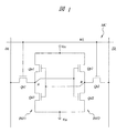
図1は、実施の形態1であるSRAMのメモリセルを示す等価回路図である。図示のように、このメモリセルMCは、一対の相補性データ線(データ線DL、データ線/(バー)DL)とワード線WLとの交差部に配置され、一対の駆動用MISFETQd1,Qd2 、一対の負荷用MISFETQp1,Qp2 および一対の転送用MISFETQt1,Qt2 により構成されている。駆動用MISFETQd1,Qd2 および転送用MISFETQt1,Qt2 はnチャネル型MISFETで構成され、負荷用MISFETQp1,Qp2 はpチャネル型MISFETで構成されている。
【0020】
メモリセルMCを構成する上記6個のMISFETのうち、駆動用MISFETQd1 および負荷用MISFETQp1 は、CMOSインバータINV1 を構成し、駆動用MISFETQd2 および負荷用MISFETQp2 は、CMOSインバータINV2 を構成している。これら一対のCMOSインバータINV1,INV2 の相互の入出力端子(蓄積ノードA、B)は、交差結合され、1ビットの情報を記憶する情報蓄積部としてのフリップフロップ回路を構成している。また、このフリップフロップ回路の一方の入出力端子(蓄積ノードA)は、転送用MISFETQt1 のソース、ドレイン領域の一方に接続され、他方の入出力端子(蓄積ノードB)は、転送用MISFETQt2 のソース、ドレイン領域の一方に接続されている。
【0021】
さらに、転送用MISFETQt1 のソース、ドレイン領域の他方はデータ線DLに接続され、転送用MISFETQt2 のソース、ドレイン領域の他方はデータ線/DLに接続されている。また、フリップフロップ回路の一端(負荷用MISFETQp1,Qp2 の各ソース領域)は電源電圧(Vcc) に接続され、他端(駆動用MISFETQd1,Qd2 の各ソース領域)は基準電圧(Vss) に接続されている。
【0022】
上記回路の動作を説明すると、一方のCMOSインバータINV1 の蓄積ノードAが高電位(“H" )であるときには、駆動用MISFETQd2 がONになるので、他方のCMOSインバータINV2 の蓄積ノードBが低電位(“L" )になる。従って、駆動用MISFETQd1 がOFFになり、蓄積ノードAの高電位(“H" )が保持される。すなわち、一対のCMOSインバータINV1,INV2 を交差結合させたラッチ回路によって相互の蓄積ノードA、Bの状態が保持され、電源電圧が印加されている間、情報が保存される。
【0023】
転送用MISFETQt1,Qt2 のそれぞれのゲート電極にはワード線WLが接続され、このワード線WLによって転送用MISFETQt1,Qt2 の導通、非導通が制御される。すなわち、ワード線WLが高電位(“H" )であるときには、転送用MISFETQt1,Qt2 がONになり、ラッチ回路と相補性データ線(データ線DL,バーDL)とが電気的に接続されるので、蓄積ノードA、Bの電位状態(“H" または“L" )がデータ線DL、/DLに現れ、メモリセルMCの情報として読み出される。
【0024】
メモリセルMCに情報を書き込むには、ワード線WLを“H" 電位レベル、転送用MISFETQt1,Qt2 をON状態にしてデータ線DL、/DLの情報を蓄積ノードA、Bに伝達する。
【0025】
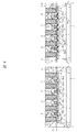
次に、本実施の形態のメモリセルの構成を図2および図3を用いて説明する。図2は、メモリセル約1個分の領域を示す半導体基板の平面図であり、図3は、図2の断面図であり、左側は、図2のA−A断面図、右側は、図2のB−B断面図を示す。なお、図2には、メモリセルを構成する各導電層とこれらの導電層を接続する接続孔のみを示し、各導電層間に形成された絶縁膜は図示しない。
【0026】
図2および図3に示すように、メモリセルMCを構成する6個のMISFET(Qt1、Qt2、Qd1、Qd2、Qp1、Qp2)のうちnチャネル型MISFET(Qt1、Qt2、Qd1、Qd2)は、活性領域Ap(p型ウエル3)上に形成されている。また、pチャネル型MISFET(Qp1、Qp2)は、活性領域An(n型ウエル4)上に形成されている。これら活性領域An、Apは、酸化シリコン膜5が埋め込まれた素子分離2で囲まれ、活性領域An、Ap上にはゲート電極Gが平行に形成されている。負荷用MISFETQp1のゲート電極および駆動用MISFETQd1のゲート電極とは共通であり、また、負荷用MISFETQp2のゲート電極および駆動用MISFETQd2のゲート電極とは共通である。
【0027】
このゲート電極Gは、多結晶シリコン膜9a、WN膜(図示せず)およびW膜9bからなり、窒化シリコン膜10およびサイドウォール膜16で、その上部および側部が覆われ、その下部にはゲート絶縁膜8が形成されている。
【0028】
また、このゲート電極Gの両側の半導体基板1中には、MISFET(Qt1、Qt2、Qd1、Qd2、Qp1、Qp2)のLDD型ソース、ドレインを構成する半導体領域13、14、17、18(図2においては図示せず)が形成されている。また、この半導体領域13、14の下部には、ポケットイオン領域PKp1、PKp2、PKn1、PKn2が形成されている。なお、このポケットイオン領域PKp1、PKp2、PKn1、PKn2の構成については、追って詳細に説明する。
【0029】
さらに、LDD型ソース、ドレインを構成する半導体領域13、14、17、18上には、ソース、ドレインと第1層配線(図示せず)との接続のためのプラグP1や、ソース、ドレインとゲート電極Gとを接続するダマシン配線MD1、DM2が形成されている。即ち、駆動用MISFETQd1のドレインは、ダマシン配線MD1により駆動用MISFETQd2のゲート電極(負荷用MISFETQp2のゲート電極)に接続され、駆動用MISFETQd2のドレインは、ダマシン配線MD2により駆動用MISFETQd1のゲート電極(負荷用MISFETQp1のゲート電極)に接続されている。なお、駆動用MISFETQd1のドレインは、後述する第1層配線により負荷用MISFETQp1のドレインに接続され、駆動用MISFETQd2のドレインは、後述する第1層配線により負荷用MISFETQp2のドレインに接続されている。また、負荷用MISFETQp1のソース(負荷用MISFETQp2のソース)は、電源電圧Vccが供給される第1層配線に接続され、駆動用MISFETQd1のソース(駆動用MISFETQd2のソース)は、基準電位Vssが供給される第1層配線に接続されている。
【0030】
図4は、上記したメモリセルMCを複数配置する場合のレイアウトを示す半導体基板1の平面図である。図中の破線で囲まれた矩形の領域は、メモリセルMC1個分の占有領域を示している。このようにメモリセルMCを繰り返しパターンで複数配置することにより、メモリセルアレイが構成される。この場合、メモリセルMC1、MC2と線対称にメモリセルMC3、MC4がレイアウトされ、メモリセルMC3、MC4と線対称にメモリセルMC5、MC6がレイアウトされている。、なお、図4には、ゲート電極Gと活性領域An、Apのみを明示し、ダマシン配線MD1、MD2およびプラグP1を省略している。
【0031】
また、図5に示すように、メモリセルアレイMC1〜MC4の周辺には、ロジック回路等が形成される周辺回路領域(図5の右側)が存在し、相補型(Complementary)のMISFET等が形成されている。図6に図5のC−C断面図を示す。図5および図6に示すように、周辺回路領域のnチャネル型MISFETおよびpチャネル型MISFETは、それぞれ活性領域Ap(p型ウエル3)および活性領域An(n型ウエル4)上に形成されている。これら活性領域An、Apは、酸化シリコン膜5が埋め込まれた素子分離2で囲まれ、活性領域An、Ap上にはゲート電極Gが平行に形成されている。nチャネル型MISFETのゲート電極およびpチャネル型MISFETのゲート電極とは共通である。
【0032】
このゲート電極Gは、多結晶シリコン膜9a、WN膜(図示せず)およびW膜9bからなり、窒化シリコン膜10およびサイドウォール膜16で、その上部および側部が覆われ、その下部にはゲート絶縁膜8が形成されている。
【0033】
また、このゲート電極Gの両側の半導体基板1中には、MISFETのLDD型ソース、ドレインを構成する半導体領域13、14、17、18(図2においては図示せず)が形成されている。また、この半導体領域13、14の下部には、ポケットイオン領域PKp1、PKp2、PKn1、PKn2が形成されている。なお、このポケットイオン領域PKp1、PKp2、PKn1、PKn2については、追って詳細に説明する。
【0034】
さらに、LDD型ソース、ドレインを構成する半導体領域13、14、17、18上には、ソース、ドレインと第1層配線(図示せず)との接続のためのプラグP1が形成されている。また、ゲート電極Gの端部には、ゲート電極Gと第1層配線等とを接続するためのコンタクト部CTが形成されている。
【0035】
次に、上記のように構成された本実施の形態のSRAMの製造方法を図7〜図29を用いて説明する。
【0036】
まず、図7および図8に示すように、半導体基板1中に素子分離2を形成する。この素子分離2は、以下のように形成する。例えば1〜10Ωcm程度の比抵抗を有するp型の単結晶シリコンからなる半導体基板1をエッチングすることにより深さ250nm程度の素子分離溝を形成する。なお、図7は、メモリセル形成領域、図8は、周辺回路形成領域を示す。
【0037】
その後、半導体基板1を約1000℃で熱酸化することによって、溝の内壁に膜厚10nm程度の薄い酸化シリコン膜(図示せず)を形成する。この酸化シリコン膜は、溝の内壁に生じたドライエッチングのダメージを回復すると共に、次の工程で溝の内部に埋め込まれる酸化シリコン膜5と半導体基板1との界面に生じるストレスを緩和するために形成する。
【0038】
次に、溝の内部を含む半導体基板1上にCVD(Chemical Vapor deposition)法で膜厚450〜500nm程度の酸化シリコン膜5を堆積し、化学的機械研磨(CMP;Chemical Mechanical Polishing)法で溝の上部の酸化シリコン膜5を研磨し、その表面を平坦化する。
【0039】
次に、半導体基板1にp型不純物(ホウ素)およびn型不純物(例えばリン)をイオン打ち込みした後、約1000℃の熱処理で上記不純物を拡散させることによって、メモリセル形成領域および周辺回路形成領域の半導体基板1にp型ウエル3およびn型ウエル4を形成する。
【0040】
次に、図9、図10に示すように、フッ酸系の洗浄液を用いて半導体基板1(p型ウエル3およびn型ウエル4)の表面をウェット洗浄した後、約800℃の熱酸化でp型ウエル3およびn型ウエル4のそれぞれの表面に膜厚6nm程度の清浄なゲート酸化膜8を形成する。なお、図9は、メモリセル形成領域、図10は、周辺回路形成領域を示す。
【0041】
次に、ゲート酸化膜8の上部に膜厚100nm程度の低抵抗多結晶シリコン膜9aをCVD法で堆積する。続いて、その上部にスパッタリング法で膜厚10nm程度のWN膜(図示せず)と膜厚50nm程度のタングステン等の高融点金属から成るW膜9bとを堆積し、さらにその上部にCVD法で膜厚200nm程度の窒化シリコン膜10を堆積する。次に、上記W膜9bの応力緩和とWN膜のデンシファイ(緻密化)とを目的として、窒素などの不活性ガス雰囲気中で約800℃の熱処理を行う。
【0042】
次に、フォトレジスト膜(図示せず)をマスクにして窒化シリコン膜10をドライエッチングすることにより、ゲート電極を形成する領域に窒化シリコン膜10を残す。
【0043】
次に、窒化シリコン膜10をマスクにしてW膜9b、WN膜(図示せず)および多結晶シリコン膜9aをドライエッチングすることにより、メモリセル形成領域および周辺回路形成領域に多結晶シリコン膜9a、WN膜およびW膜9bからなるゲート電極Gを形成する。
【0044】
次に、メモリセル形成領域および周辺回路形成領域のp型ウエル3上のゲート電極Gの両側にn型不純物(リン)を注入することによってn-型半導体領域13を形成し、また、メモリセル形成領域および周辺回路形成領域のn型ウエル4上にp型不純物(ヒ素)を注入することによってp-型半導体領域14を形成する。
【0045】
次いで、短チャネル効果を抑制するため、メモリセル形成領域および周辺回路形成領域のn-型半導体領域13の下部に、p型不純物を注入することによってp型ポケットイオン領域PKp1、PKp2を形成し、また、p-型半導体領域14の下部に、n型不純物を注入することによってn型ポケットイオン領域PKn1、PKn2を形成する。
【0046】
このp型およびn型のポケットイオン領域PKp1、PKp2、PKn1、PKn2の形成工程を図11〜図21までを参照しながら詳細に説明する。
【0047】
まず、nチャネル型MISFET上をレジスト膜で覆い、pチャネル型MISFET形成領域にn型ポケットイオンPKn1、PKn2領域を形成する。
【0048】
図11は、メモリセル形成領域のpチャネル型MISFET、例えばQd1のゲート電極Gおよびソース、ドレイン領域の拡大図である。図12は、周辺回路形成領域のpチャネル型MISFETのゲート電極Gおよびソース、ドレイン領域の拡大図である。
【0049】
図11および図12に示すように、メモリセル形成領域および周辺回路形成領域のn型ウエル上4のゲート電極Gの両側にn型不純物(リン)を注入する。この不純物の注入に際しては、p-型半導体領域14の下部のみならず、p-型半導体領域14の下部からゲート電極Gの下部(チャネル領域)まで不純物を注入するため、いわゆる斜めイオン注入法を用いて不純物の注入を行う。この際、周辺回路領域においては、ゲート電極が紙面縦方向(図5参照)のみならず横方向にも延在し得るため、ゲート電極に対し4方向から不純物の注入を行う。
【0050】
ここで、4方向とは、図13(a)および(b)に示すように、ゲート電極の長さ方向の側面L1に対してθの角度であって、半導体基板表面に対して(90°−θ)の角度である第1方向(1)、ゲート電極の長さ方向の側面L2に対してθの角度であって、半導体基板表面に対して(90°−θ)の角度である第2方向(2)、ゲート電極の幅方向の側面H1に対してθの角度であって、半導体基板表面に対して(90°−θ)の角度である第3方向(3)およびゲート電極の幅方向の側面H2に対してθの角度であって、半導体基板表面に対して(90°−θ)の角度である第4方向(4)をいう。図13(a)は、ゲート電極に対する不純物の注入方向を上面から見た図で、図13(b)は、ゲート電極の断面図に対する不純物の注入方向を示した図である。
【0051】
また、図13(b)に示すように、第1方向(1)および第2方向(2)からの不純物の注入により浅くかつゲート電極Gの下部(チャネル領域)まで延在する第1のポケットイオン領域PKn1が形成され、第3方向(3)および第4方向(4)からの不純物の注入により第1のポケットイオン領域より深い第2のポケットイオン領域PKn2が形成される。
【0052】
しかしながら、図14に示すように、メモリセル形成領域においては、pチャネル型MISFETQp1、Qp2のポケットイオン注入時には、nチャネル型MISFETQt1、Qt2、Qd1、Qd2形成領域上がレジスト膜Rn1、Rn2で覆われており、メモリセルMC1、MC2のpチャネル型MISFETQp1、Qp2形成領域は、レジスト膜Rn1による遮蔽領域S1内に存在するため、前記第3方向(3)から注入される不純物は注入されない(図15(a)参照)。一方、メモリセルMC3、MC4のpチャネル型MISFETQp1、Qp2kレイ正領域は、レジスト膜Rn2による遮蔽領域S2内に存在するため、前記第4方向(4)から注入される不純物は注入されない(図15(b)参照)。なお、図15(a)は、図14のD−D断面図、図15(b)は、図14のE−E断面図である。
【0053】
従って、図11および図15に示す、第1のポケットイオン領域PKn1は、第1方向(1)および第2方向(2)の2方向から不純物が注入されるのに対し、第2のポケットイオン領域PKn2は、第3方向(3)もしくは第4方向(4)の1方向からしか不純物が注入されないため、第2のポケットイオン領域PKn2は、第1のポケットイオン領域PKn1より不純物濃度が低くなる。
【0054】
また、前記遮蔽領域S1、S2とは、レジスト膜Rn1およびRn2のpチャネル型MISFETの側の端部PRn1、PRn2から、レジスト膜の膜厚Hと不純物注入角度θのtanとの積から得られる距離S(S=Htanθ)だけ離れた領域をいう。なお、レジスト膜Rn1、Rn2は、本来レジストで覆うべき領域(この場合、活性領域Ap)およびその端部からマスク合わせ時のずれ量を考慮した合わせ余裕分離れた領域を少なくとも覆う必要がある。なお、本実施の形態の場合、レジスト膜の膜厚Hは、1.0μm、不純物注入角度θは、20°であり、距離Sは、0.36μmとなる。
【0055】
このように、pチャネル型MISFETQp1、Qp2を遮蔽領域S1、S2内に形成したのでのpチャネル型MISFETQp1、Qp2のポケットイオン注入時には、第3方向(3)もしくは第4方向(4)の1方向からしか不純物が注入されないため、レジスト膜のマスクずれにより第2のポケットイオン領域PKn2の不純物濃度のばらつきによる閾値電圧Vthのばらつきを防止することができる。
【0056】
また、pチャネル型MISFETQp1、Qp2を遮蔽領域S1、S2内に形成したのでセル面積の縮小化を図ることができる。
【0057】
即ち、図16(a)に示すように、前記第1〜第4方向すべてから不純物を注入する場合、前記遮蔽領域S1、S2を避けてpチャネル型MISFETQp1、Qp2を形成する必要があり、即ち、pチャネル型MISFETQp1、Qp2形成領域を、少なくともレジスト膜の端部PRn1、PRn2からレジスト膜の膜厚Hと不純物注入角度θのtanとの積から得られる距離S1、S2離さなければならず、セル面積の縮小化が困難であった。
【0058】
また、pチャネル型MISFETQp1、Qp2形成領域を、少なくともレジスト膜の端部PRn1、PRn2からレジスト膜の膜厚Hと不純物注入角度θのtanとの積から得られる距離S1、S2離したレイアウトとしても、レジスト膜形成時にマスクずれが生じた場合(図16(b))には、pチャネル型MISFETQp1、Qp2形成領域中に、前記第1〜第4方向すべてから不純物を注入される領域αとレジスト膜に遮蔽され不純物を注入することができない領域βが生じ、第2のポケットイオン領域PKn2の不純物濃度にばらつきが生じる。この不純物濃度のばらつきによりMISFETの閾値電圧Vthがばらついてしまう。
【0059】
しかしながら、前述の通り本実施の形態においては、閾値電圧Vthのばらつきを防止することができ、また、セル面積の縮小化を図ることができる。
【0060】
一方、図17に示すように、周辺回路形成領域においては、nチャネル型MISFET形成領域上がレジスト膜Rn3で覆われているが、pチャネル型MISFET形成領域は、レジスト膜Rn3による遮蔽領域S3を避けて設けられている。即ち、本実施の形態の場合、レジスト膜の膜厚Hは、1.0μm、不純物注入角度θは、20°であるため、S3は、0.36μmとなるが、本実施の形態の場合、周辺回路形成領域においては、pチャネル型MISFET形成領域Anとnチャネル型MISFET形成領域Apとの距離は、0.8μmであるため、前記第1〜第4方向すべてから不純物が注入される。
【0061】
従って、図12に示す周辺回路形成領域の第2のポケットイオン領域PKn2は、第3方向(3)もしくは第4方向(4)の1方向からしか不純物が注入されないメモリセル形成領域の第2のポケットイオン領域PKn2(図11)より不純物濃度が高くなる。
【0062】
次いで、レジスト膜Rn1、Rn2およびRn3を除去し、pチャネル型MISFET形成領域上をレジスト膜Rp1、Rp2等で覆い、nチャネル型MISFET形成領域にp型ポケットイオン領域PKp1、PKp2を形成する。なお、p型ポケットイオン領域PKp1、PKp2を形成した後、n型ポケットイオン領域PKn1、PKn2を形成してもよい。
【0063】
図18は、メモリセル形成領域のnチャネル型MISFET、例えばQd1のゲート電極Gおよびソース、ドレイン領域の拡大図である。図19は、周辺回路形成領域のnチャネル型MISFETのゲート電極Gおよびソース、ドレイン領域の拡大図である。
【0064】
図18および図19に示すように、メモリセル形成領域および周辺回路形成領域のp型ウエル3上のゲート電極Gの両側にp型不純物(ヒ素)を注入する。この不純物の注入の際も、n型ポケットイオン領域PKn1、PKn2形成時と同様に、斜めイオン注入法を用いて、ゲート電極Gに対し4方向から不純物の注入を行う。
【0065】
また、図20に示すように、メモリセル形成領域においては、nチャネル型MISFETQt1、Qt2、Qd1、Qd2のポケットイオン注入時には、pチャネル型MISFET2Qp1、Qp2形成領域上がレジスト膜Rp1、Rp2で覆われており、メモリセルMC3、MC4のnチャネル型MISFETQt1、Qt2、Qd1、Qd2形成領域は、レジスト膜Rp1による遮蔽領域S4内に存在するため、前記第3方向から注入される不純物は注入されない。一方、メモリセルMC5、MC6のnチャネル型MISFETQt1、Qt2、Qd1、Qd2形成領域は、レジスト膜Rp2による遮蔽領域S5内に存在するため、前記第4方向から注入される不純物は注入されない。
【0066】
従って、図18に示す、第1のポケットイオン領域PKp1は、第1方向(1)および第2方向(2)の2方向から不純物が注入されるのに対し、第2のポケットイオン領域PKp2は、第3方向(3)もしくは第4方向(4)の1方向からしか不純物が注入されないため、第2のポケットイオン領域PKp2は、第1のポケットイオン領域PKp1より不純物濃度が低くなる。
【0067】
一方、図21に示すように、周辺回路領域においては、pチャネル型MISFET形成領域上がレジスト膜Rp3で覆われているが、nチャネル型MISFET形成領域は、レジスト膜Rp3による遮蔽領域S6を避けて設けられているため、pチャネル型MISFETのゲート電極Gにおいては、前記第1〜第4方向すべてから不純物を注入される。
【0068】
従って、図19に示す周辺回路形成領域の第2のポケットイオン領域PKp2は、第3方向(3)もしくは第4方向(4)の1方向からしか不純物が注入されないメモリセル形成領域の第2のポケットイオン領域PKp2(図18)より不純物濃度が高くなる。
【0069】
このように、nチャネル型MISFETMISFETQt1、Qt2、Qd1、Qd2形成領域を遮蔽領域S4、S5内に形成したのでnチャネル型MISFETQt1、Qt2、Qd1、Qd2のポケットイオン注入時には、第3方向(3)もしくは第4方向(4)の1方向からしか不純物が注入されないため、p型ポケットイオン領域形成時と同様に、レジスト膜Rp1、Rp2のマスクずれにより第2のポケットイオン領域PKp2の不純物濃度のばらつきによる閾値電圧Vthのばらつきを防止することができる。
【0070】
また、nチャネル型MISFETQt1、Qt2、Qd1、Qd2形成領域を遮蔽領域S4、S5内に形成したのでセル面積の縮小化を図ることができる。
【0071】
次いで、図22および図23に示すように、半導体基板1上にCVD法で膜厚40nm程度の窒化シリコン膜を堆積した後、異方的にエッチングすることによって、ゲート電極Gの側壁にサイドウォールスペーサ16を形成する。なお、図22は、メモリセル形成領域、図23は、周辺回路形成領域を示す。
【0072】
次に、p型ウエル3にn型不純物(リンまたはヒ素)をイオン打ち込みすることによってn+型半導体領域17(ソース、ドレイン)を形成し、n型ウエル4にp型不純物(ホウ素)をイオン打ち込みすることによってp+型半導体領域18(ソース、ドレイン)を形成する。
【0073】
ここまでの工程で、メモリセルMCを構成する6個のMISFET(駆動用MISFETQd1,Qd2 、転送用MISFETQt1,Qt2 および負荷用MISFETQp1,Qp2 )および周辺回路を構成するnチャネル型MISFETおよびpチャネル型MISFETが完成する。
【0074】
続いて、図24、25に示すように、半導体基板1の表面を洗浄した後、半導体基板1の露出部(n+型半導体領域17、p+型半導体領域18)上に、シリコン膜を選択成長させる。次いで、スパッタ法によりCo膜およびTi膜を順次堆積する。次いで、600℃で1分間の熱処理を施し、前記シリコン膜とCo膜との接触部にCoSi2層19を形成する。なお、図24は、メモリセル形成領域、図25は、周辺回路形成領域を示す。
【0075】
次いで、未反応のCo膜およびTi膜をエッチングにより除去した後、700から800℃で、1分間程度の熱処理を施し、CoSi2層19を低抵抗化する。
【0076】
次いで、半導体基板1上にCVD法で膜厚50nm程度の窒化シリコン膜20を堆積し、続いて窒化シリコン膜17の上部にCVD法で膜厚700nm〜800nm程度の酸化シリコン膜21を堆積した後、酸化シリコン膜21をCMP法で研磨してその表面を平坦化する。なお、窒化シリコン膜17は、後述するコンタクトホールC1等の形成時のエッチングストッパーとしての役割を果たす。
【0077】
次に、フォトレジスト膜(図示せず)をマスクにしたドライエッチングで酸化シリコン膜21をドライエッチングし、続いて窒化シリコン膜20をドライエッチングすることによって、n+型半導体領域17(ソース、ドレイン)およびp+型半導体領域18(ソース、ドレイン)上にコンタクトホールC1および配線溝HMDを形成する。なお、この配線溝HMDは、MISFETQd1、Qd2のゲート電極G上まで延在している(図2)。
【0078】
次いで、コンタクトホールC1および配線溝HMD内に導電性膜を埋め込むことによりプラグP1および配線MD1、MD2を形成する。まず、コンタクトホールC1および配線溝HMDの内部を含む酸化シリコン膜21の上部にスパッタ法により膜厚10nm程度のTi膜(図示せず)および膜厚50nm程度のTiN膜を順次し、500〜700℃で1分間熱処理を施す。次いでCVD法によりW膜を堆積し、エッチバックもしくはCMPを施し、コンタクトホール外部のTi膜、TiN膜およびW膜を除去することによりプラグP1および配線MD1、MD2を形成する。
【0079】
以上の工程により、図2および図3を用いて説明したSRAMメモリセルおよびその周辺回路が形成される。
【0080】
この後、プラグP1および配線MD上に第1層配線M1および第2層配線M2が形成される。引き続き、これらの配線の形成工程について説明する。
【0081】
続いて、図24、25に示すように、酸化シリコン膜21、プラグP1および配線MD上に、酸化シリコン膜22、23を順次CVD法により堆積する。次に、プラグP1および配線MD1、MD2と第1層配線とのコンタクト領域上の酸化シリコン膜23、22をエッチングにより除去することによりコンタクトホールC2を形成する。
【0082】
次いで、コンタクトホールC2内を含む酸化シリコン膜23上に反射防止膜(図示せず)を形成し、コンタクトホールC2内を反射防止膜で埋め込む。さらに、第1層配線形成予定領域上の反射防止膜および酸化シリコン膜23をエッチングすることにより配線溝HM1を形成する。次に、コンタクトホール内C2に残存した反射防止膜を除去しする。以上の工程により、第1層配線用の配線溝HM1と、第2層配線とプラグP1および配線MDとを接続するためのコンタクトホールC2が形成される。
【0083】
なお、第1層配線形成予定領域上の酸化シリコン膜23をエッチングすることにより、配線溝HM1を形成した後、配線溝HM1内を反射防止膜等で埋め込んだ後、コンタクトホールC2を形成してもよい。また、酸化シリコン膜22、23の膜種を変更すれば、エッチングレートが異なり、容易にコンタクトホールC2および配線溝HM1を形成することができる。また、酸化シリコン膜22と23との間に、エッチングストッパーとして窒化シリコン膜を形成してもよい。
【0084】
次に、配線溝HM1およびコンタクトホールC2内を含む酸化シリコン膜23上に窒化チタンからなるバリア層をCVD法により堆積し、次いで、バリア層上に銅膜を電解メッキ法により形成する。次に、配線溝HM1およびコンタクトホールC2外部の銅膜およびバリア層をCMPにより除去して、第1層配線M1および第1層配線M1と配線MD1、MD2およびプラグP1との接続部を形成する。
【0085】
図26に、第1層配線M1形成後のメモリセル約1個分の領域を示す半導体基板の平面図を示す。
【0086】
次に、図27および図28に示すように、酸化シリコン膜23および第1層配線M1に、第1層配線M1を構成する銅膜の拡散を防止するために、窒化シリコン膜24をCVD法により堆積した後、第1層配線と同様に、第2層配線を形成する。まず、酸化シリコン膜25、26を順次堆積し、第1層配線M1と第2層配線とのコンタクト領域上の酸化シリコン膜25、26および窒化シリコン膜24をエッチングにより除去することによりコンタクトホールC3を形成する。なお、図27は、メモリセル形成領域、図28は、周辺回路形成領域を示す。
【0087】
次いで、コンタクトホールC3内を含む酸化シリコン膜26上に反射防止膜(図示せず)を形成し、コンタクトホールC3内を反射防止膜で埋め込む。さらに、第2層配線形成予定領域上の反射防止膜および酸化シリコン膜26をエッチングすることにより配線溝HM2を形成する。次に、コンタクトホールC3内に残存した反射防止膜を除去しする。
【0088】
次に、配線溝HM2およびコンタクトホールC3内を含む酸化シリコン膜26上に窒化チタンからなるバリア層をCVD法により堆積し、次いで、バリア層上に銅膜を電解メッキ法により形成する。次に、配線溝HM2およびコンタクトホールC3外部の銅膜およびバリア層をCMPにより除去して、第2層配線M2および第1層配線M1と第2層配線M2との接続部を形成する。
【0089】
図29に、第2層配線M2形成後のメモリセル約1個分の領域を示す半導体基板の平面図を示す。
【0090】
なお、本実施の形態においては、第1層配線M1および第2層配線M2の形成に際し、これら配線と下層配線との接続部を同時に形成するいわゆるデュアルダマシン法を用いたが、接続部を形成した後、配線を形成するシングルダマシン法を用いることも可能である。
【0091】
(実施の形態2)
図30は、実施の形態2であるのSRAMのメモリセルを示す等価回路図である。図30に示すように、、駆動用MISFETQd1 および負荷用MISFETQp1のゲート電極部と、駆動用MISFETQd2 および負荷用MISFETQp2のゲート電極部に、容量素子Cが接続されている。その他の構成は、実施の形態1の場合と同じであるためその説明を省略する。
【0092】
次に、実施の形態2であるのSRAMのの製造方法を図31〜図35を用いて説明する。なお、周辺回路形成領域については、実施の形態1の場合と同様であるため、メモリセル形成領域についてのみ説明する。また、メモリセル形成領域において、図22を用いて説明したサイドウォール16形成工程までは、実施の形態1の場合と同様であるためその説明を省略する。
【0093】
まず、実施の形態1で説明した図22に示す半導体基板1を準備し、図31に示すように、半導体基板1上にCVD法で膜厚50nm程度の窒化シリコン膜20を堆積し、続いて窒化シリコン膜20の上部にCVD法で膜厚700nm〜800nm程度の酸化シリコン膜21を堆積した後、酸化シリコン膜21をCMP法で研磨してその表面を平坦化する。なお、窒化シリコン膜20は、後述するコンタクトホールC1等の形成時のエッチングストッパーとしての役割を果たす。
【0094】
次に、フォトレジスト膜(図示せず)をマスクにしたドライエッチングで酸化シリコン膜21をドライエッチングし、続いて窒化シリコン膜20をドライエッチングすることによって、n+型半導体領域17(ソース、ドレイン)およびp+型半導体領域18(ソース、ドレイン)上にコンタクトホールC1および配線溝HMD1、HMD22を形成する。ここで、図32に示すように、配線溝HMD1は、MISFETQd2のゲート電極上まで延在し、配線溝HMD22は、MISFETQd1のゲート電極上およびMISFETQp2のドレイン領域まで延在している。
【0095】
次いで、コンタクトホールC1および配線溝HMD1、HMD22内に導電性膜を埋め込むことによりプラグP1および配線MD1、MD22を形成する。まず、コンタクトホールC1および配線溝HMD1、HMD22の内部を含む酸化シリコン膜21の上部にスパッタ法により膜厚10nm程度のTi膜(図示せず)および膜厚50nm程度のTiN膜を順次し、500〜700℃で1分間熱処理を施す。次いでCVD法によりW膜を堆積し、エッチバックもしくはCMPを施し、コンタクトホール外部のTi膜、TiN膜およびW膜を除去することによりプラグP1および配線MD1、MD22を形成する。この配線MD22は、前述したように、MISFETQd1のゲート電極上およびMISFETQp2のドレイン領域まで延在している(図32)。
【0096】
続いて、酸化シリコン膜21上に窒化シリコン膜201を形成しする。この窒化シリコン膜201は、下部電極となる配線MD22と後述する上部電極ULとの間に形成され、容量絶縁膜となる。
【0097】
次に、窒化シリコン膜201上に、スパッタ法によりTiN膜を堆積し、パターニングすることによって、配線MD22上およびMISFETQd1のソースとMISFETQp1のドレイン間上に延在する上部電極ULを形成する(図33)。
【0098】
このように本実施の形態においては、実施の形態1と同様に、MISFETQt1、Qt2、Qd1、Qd2、Qp1、Qp2を遮蔽領域S1、S2内に形成したのでポケットイオン注入時には、第3方向(3)もしくは第4方向(4)の1方向からしか不純物が注入されないため、第2のポケットイオン領域PKn2、PKp2の不純物濃度のばらつきによる閾値電圧Vthのばらつきを防止することができる。また、セル面積の縮小化を図ることができる。
【0099】
さらに、クロスカップル間(図31のノードAB間)に配線MD22、窒化シリコン膜201および下部電極ULから成る容量素子Cを形成したので、情報をより安定して保持することができる。即ち、第2のポケットイオン領域PKn2、PKp2に1方向からしか不純物が注入されないため閾値電位Vtが低下し、サージ電圧等によりMISFETQp1等が動作してしまう恐れがある。しかしながら、クロスカップル間(ノードAB間)に容量素子Cを形成しておけば、この容量素子Cにサージ電圧等による電化が蓄積される。従って、MISFETの情報をより安定して保持することができる。
【0100】
次に、上部電極UL上に、実施の形態1の場合と同様に、第1層配線M1および第2層配線M2を形成する。
【0101】
まず、プラグP1、配線MD1および上部電極UL上に、酸化シリコン膜22、23を順次CVD法により堆積する。次いで、プラグP1および配線MD1と第1層配線とのコンタクト領域上の酸化シリコン膜23、22をエッチングにより除去することによりコンタクトホールC2を形成する、次いで、コンタクトホールC3内を反射防止膜(図示せず)で埋め込む。さらに、第1層配線形成予定領域上の反射防止膜および酸化シリコン膜26をエッチングすることにより配線溝HM2を形成する。なお、配線溝HM1を形成した後、コンタクトホールC2を形成してもよい。また、酸化シリコン膜22、23の膜種を変更することにより、容易にコンタクトホールC2および配線溝HM1を形成することができる。また、酸化シリコン膜22と23との間に、エッチングストッパーとして窒化シリコン膜を形成してもよい。
【0102】
次に、配線溝HM1およびコンタクトホールC2内を含む酸化シリコン膜23上に窒化チタンからなるバリア層をCVD法により堆積し、次いで、バリア層上に銅膜を電解メッキ法により形成する。次に、配線溝HM1およびコンタクトホールC2外部の銅膜およびバリア層をCMPにより除去して、第1層配線M1および第1層配線M1と配線MD1、MD22およびプラグP1との接続部を形成する。
【0103】
図34に、第1層配線形成後のメモリセル約1個分の領域を示す半導体基板の平面図を示す。
【0104】
次に、酸化シリコン膜23および第1層配線M1に、第1層配線を構成する銅膜の拡散を防止するために、窒化シリコン膜24をCVD法により堆積した後、酸化シリコン膜25、26を順次堆積する。次に、第1層配線M1と第2層配線とのコンタクト領域上の酸化シリコン膜25、26および窒化シリコン膜24をエッチングにより除去することによりコンタクトホールC3を形成する。
【0105】
次いで、コンタクトホールC3内を反射防止膜(図示せず)で埋め込み、さらに、第2層配線形成予定領域上の反射防止膜および酸化シリコン膜26をエッチングすることにより配線溝HM2を形成する。
【0106】
次に、配線溝HM2およびコンタクトホールC3内を含む酸化シリコン膜26上に窒化チタンからなるバリア層をCVD法により堆積し、次いで、バリア層上に銅膜を電解メッキ法により形成する。次に、配線溝HM2およびコンタクトホールC3外部の銅膜およびバリア層をCMPにより除去して、第2層配線M2および第1層配線M1と第2層配線M2との接続部を形成する。
【0107】
図35に、第2層配線M2形成後のメモリセル約1個分の領域を示す半導体基板の平面図を示す。
【0108】
なお、本実施の形態においては、第1層配線および第2層配線の形成に際し、これら配線と下層配線との接続部を同時に形成するいわゆるデュアルダマシン法を用いたが、接続部を形成した後、配線を形成するシングルダマシン法を用いることも可能である。
【0109】
(実施の形態3)
実施の形態1および2においては、メモリセル形成領域および周辺回路形成領域のnチャネル型MISFETのポケットイオン領域PKp1、PKp2を同一工程で形成したが、別工程で形成することも可能である。即ち、メモリセル形成領域のポケットイオン注入の際には、周辺回路形成領域をレジスト膜で覆い、メモリセル形成領域のnチャネル型MISFETのポケットイオン領域PKp1、PKp2形成後、周辺回路形成領域のポケットイオン領域PKp1、PKp2を形成する。pチャネル型MISFETのポケットイオン領域PKn1、PKn2についても同様である。
【0110】
また、この際、メモリセル形成領域のポケットイオン注入時には、実施の形態1で説明した第1および第2の方向からのみ不純物注入を行うことも可能である。この場合、メモリセル形成領域の第2のポケットイオン領域PKn2、PKp2は形成されない。従って、第2のポケットイオン領域PKn2、PKp2の不純物濃度のばらつきによる閾値電圧Vthのばらつきを防止することができる。
【0111】
以上、本発明者によってなされた発明を実施の形態に基づき具体的に説明したが、本発明は前記実施の形態に限定されるものではなく、その要旨を逸脱しない範囲で種々変更可能であることはいうまでもない。
【0112】
特に、本発明においては、微細化が要求されるSRAMのメモリセル形成領域に本発明を適用したが、図36に示すようなDRAM(Dynamic Random Access Memory)内部に形成されるセンスアンプ部SA等、微細な領域にnチャネル型MISFETおよびpチャネル型MISFETが形成される半導体集積回路装置に広く適用することができる。なお、図36中、DMCは、DRAMメモリセルを示し、転送用MISFETQSとキャパシタCとから成り、ワード線WLとビット線BLに接続されている。また、センスアンプ部SAは、交差結合された一対のCMOSインバータINV1,INV2 から成り、ビット線BL間に接続されている。
【0113】
【発明の効果】
本願において開示される発明のうち、代表的なものによって得られる効果を簡単に説明すれば以下のとおりである。
【0114】
本発明によれば、第1の領域(例えば、pチャネル型MISFET形成領域)を、ポケットイオン領域を形成する際に第2の領域(例えば、nチャネル型MISFET形成領域)上に形成されるレジスト膜の端部から、前記レジスト膜の膜厚Hおよびイオン注入角度θとのtanの積である距離S1以内に配置し、斜めイオン注入を行ったので、4方向から注入される不純物のうち一方向からの不純物が注入されないため、第1の領域内のMISFETのポケットイオン領域の不純物濃度のばらつきを抑え、閾値電圧Vthのばらつきを防止することができる。また、面積の縮小化を図ることができる。
【図面の簡単な説明】
【図1】本発明の実施の形態1であるSRAMのメモリセルを示す等価回路図である。
【図2】本発明の実施の形態1であるSRAMメモリセル約1個分の領域を示す半導体基板の平面図である。
【図3】本発明の実施の形態1であるSRAMメモリセル約1個分の領域を示す半導体基板の断面図である。
【図4】本発明の実施の形態1であるSRAMメモリセル形成領域を示す半導体基板の要部平面図である。
【図5】本発明の実施の形態1であるSRAMメモリセル形成領域および周辺回路形成領域を示す半導体基板の要部平面図である。
【図6】本発明の実施の形態1であるSRAM周辺回路形成領域を示す半導体基板の要部断面図である。
【図7】本発明の実施の形態1であるSRAMメモリセル形成領域の製造方法を示す半導体基板の要部断面図である。
【図8】本発明の実施の形態1であるSRAM周辺回路形成領域の製造方法を示す半導体基板の要部断面図である。
【図9】本発明の実施の形態1であるSRAMメモリセル形成領域の製造方法を示す半導体基板の要部断面図である。
【図10】本発明の実施の形態1であるSRAM周辺回路形成領域の製造方法を示す半導体基板の要部断面図である。
【図11】本発明の実施の形態1であるSRAMメモリセル形成領域の製造方法を示す半導体基板の要部断面図である。
【図12】本発明の実施の形態1であるSRAM周辺回路形成領域の製造方法を示す半導体基板の要部断面図である。
【図13】本発明の実施の形態1であるSRAMメモリセル形成領域および周辺回路形成領域の製造方法を示す半導体基板の要部断面図である。
【図14】本発明の実施の形態1であるSRAMメモリセル形成領域の製造方法を示す半導体基板の要部平面図である。
【図15】本発明の実施の形態1であるSRAMメモリセル形成領域の製造方法を示す半導体基板の要部断面図である。
【図16】本発明の効果を示すための図である。
【図17】本発明の実施の形態1であるSRAM周辺回路形成領域の製造方法を示す半導体基板の要部平面図である。
【図18】本発明の実施の形態1であるSRAMメモリセル形成領域の製造方法を示す半導体基板の要部断面図である。
【図19】本発明の実施の形態1であるSRAM周辺回路形成領域の製造方法を示す半導体基板の要部断面図である。
【図20】本発明の実施の形態1であるSRAMメモリセル形成領域の製造方法を示す半導体基板の要部平面図である。
【図21】本発明の実施の形態1であるSRAM周辺回路形成領域の製造方法を示す半導体基板の要部断面図である。
【図22】本発明の実施の形態1であるSRAMメモリセル形成領域の製造方法を示す半導体基板の要部断面図である。
【図23】本発明の実施の形態1であるSRAM周辺回路形成領域の製造方法を示す半導体基板の要部断面図である。
【図24】本発明の実施の形態1であるSRAMメモリセル形成領域の製造方法を示す半導体基板の要部断面図である。
【図25】本発明の実施の形態1であるSRAM周辺回路形成領域の製造方法を示す半導体基板の要部断面図である。
【図26】本発明の実施の形態1であるSRAMメモリセル形成領域の製造方法を示す半導体基板の要部平面図である。
【図27】本発明の実施の形態1であるSRAMメモリセル形成領域の製造方法を示す半導体基板の要部断面図である。
【図28】本発明の実施の形態1であるSRAM周辺回路形成領域の製造方法を示す半導体基板の要部断面図である。
【図29】本発明の実施の形態1であるSRAMメモリセル形成領域の製造方法を示す半導体基板の要部平面図である。
【図30】本発明の実施の形態2であるSRAMのメモリセルを示す等価回路図である。
【図31】本発明の実施の形態2であるSRAMメモリセル形成領域の製造方法を示す半導体基板の要部断面図である。
【図32】本発明の実施の形態2であるSRAMメモリセル形成領域の製造方法を示す半導体基板の要部平面図である。
【図33】本発明の実施の形態1であるSRAMメモリセル形成領域の製造方法を示す半導体基板の要部平面図である。
【図34】本発明の実施の形態2であるSRAMメモリセル形成領域の製造方法を示す半導体基板の要部平面図である。
【図35】本発明の実施の形態2であるSRAMメモリセル形成領域の製造方法を示す半導体基板の要部平面図である。
【図36】本発明の他の実施の形態であるDRAMメモリセル内のセンスアンプ部を示す回路図である。
【符号の説明】
1 半導体基板
2 素子分離
3 p型ウエル
4 n型ウエル
5 酸化シリコン膜
8 ゲート酸化膜
G ゲート電極
9a 多結晶シリコン膜
9b W膜
10 酸化シリコン膜
13 n-型半導体領域
14 p-型半導体領域
PKp1、PKn1 第1のポケットイオン領域
PKp2、PKn2 第2のポケットイオン領域
16 サイドウォールスペーサ
17 n+型半導体領域
18 p+型半導体領域
19 CoSi膜
20 窒化シリコン膜
21 酸化シリコン膜
C1 コンタクトホール
P1 プラグ
MD1、MD2 配線
HMD 配線溝
L1、L2 ゲート側面
H1、H2 ゲート側面
Rn1、Rn2 レジスト膜
PRn1、PRn2 レジスト膜端部
S1、S2 遮蔽領域
H レジスト膜圧
θ イオン注入角度
α 不純物が注入される領域
β 不純物を注入することができない領域
Rn3 レジスト膜
S3 遮蔽領域
S4、S5 遮蔽領域
Rp1、Rp2 レジスト膜
PRp1、PRp2 レジスト膜端部
Rp3 レジスト膜
S6 遮蔽領域17
22、23 酸化シリコン膜
C2 コンタクトホール
HM1 配線溝
M1 第1層配線
24 窒化シリコン膜
25、26 酸化シリコン膜
C3 コンタクトホール
HM1、HM22 配線溝
M2 第2層配線
MD22 配線
201 窒化シリコン膜
UL 上部電極
MCMC1〜MC6 メモリセル
CT コンタクトホール
WL ワードライン
DL、/DL データ線
Qt1、Qt2 転送用MISFET
Qd1、Qd2 駆動用MISFET
Qp1、Qp2 負荷用MISFET
Vcc 電源電圧
Vss 基準電圧
INV1、INV2 インバータ
A、B 蓄積ノード
Ap p型活性領域
An n型活性領域
C 外部容量
DMC DRAMメモリセル
BL ビット線
SA センスアンプ
CT コンタクトホール
L1、L2、H1、H2 ゲート電極側面[0001]
BACKGROUND OF THE INVENTION
The present invention relates to a semiconductor integrated circuit device and a manufacturing technique thereof, and more particularly to a semiconductor integrated circuit device having an SRAM (Static Random Access Memory) in which memory cells are configured by using six MISFETs (Metal Insulator Semiconductor Field Effect Transistors). It is related to effective technology when applied.
[0002]
[Prior art]
For a cache memory for a personal computer or a workstation, an SRAM in which memory cells are configured using six MISFETs is used. This type of SRAM is described in, for example, JP-A-9-129753, JP-A-9-55440, JP-A-9-36252, and the like.
[0003]
On the other hand, with the miniaturization of the MISFET, there is a problem of a decrease in breakdown voltage between the source and drain due to the short channel effect. That is, when the channel length (the width of the gate electrode) is shortened with the miniaturization of the MISFET, the depletion layers extending from the source and the drain are connected. In such a state, since the drain electric field affects the source and lowers the diffusion potential in the vicinity of the source, a current flows between the source and the drain even if a channel is not formed (punch-through phenomenon). When this punch-through phenomenon starts to occur, the drain current rapidly increases with an increase in the drain voltage, and the saturation current stops flowing.
[0004]
Therefore, an LDD (Lightly doped Drain) structure source / drain structure composed of a low-concentration semiconductor region and a high-concentration semiconductor region is adopted, and further, impurities constituting the source / drain are below the source / drain. By forming a region (pocket ion region) composed of impurities of the opposite conductivity type, the spread of the depletion layer extending from the source and drain is suppressed, and the occurrence of the punch-through phenomenon is suppressed.
[0005]
[Problems to be solved by the invention]
It is effective to form this pocket ion region not only under the source and drain but also from the source and drain to the channel region. At this time, since the gate electrode exists on the channel region, it is necessary to form the pocket ion region by using the oblique ion implantation method.
[0006]
On the other hand, as described above, the SRAM cell has a total of six MISFETs including two drive n-channel MISFETs, two transfer n-channel MISFETs, and two load p-channel MISFETs. The n-channel MISFET for driving and the two p-channel MISFETs for load constitute a pair of CMOS inverters.
[0007]
Therefore, in order to perform the above-described ion implantation for forming the pocket ion region (hereinafter referred to as pocket ion implantation), the driving n-channel MISFET and the transfer n-channel MISFET are first covered with a resist film, and then used for loading. It is necessary to perform pocket ion implantation for the p-channel MISFET so that pocket ions (n-type) for the p-channel MISFET are not implanted into the n-channel MISFET. Conversely, when pocket ion implantation of the driving n-channel MISFET and the transfer n-channel MISFET is performed, the load p-channel MISFET is covered with a resist film, and the p-channel MISFET is covered with a pocket for the n-channel MISFET. Do not implant ions (p-type).
[0008]
Furthermore, in the region where the p-channel MISFET and the n-channel MISFET are close to each other, pocket ions cannot be implanted into the region shielded by the resist film. Therefore, as will be described in detail later, the distance S between the resist film end on the n-channel MISFET and the active region where the p-channel MISFET is formed is equal to the resist film thickness H and the tan of the ion implantation angle θ. The active region in which the p-channel type MISFET is formed is arranged so as to be larger than the product (S> Htanθ). Similarly, in the case of the active region where the n-channel MISFET is formed, the distance S between the resist film end on the p-channel MISFET and the active region where the n-channel MISFET is formed is equal to the resist film thickness H. The ion implantation angle θ is arranged to be larger than the product of tan and (S> H tan θ).
[0009]
However, since the resist film thickness H and the ion implantation angle θ are almost specified values in order to ensure the resist material, its exposure accuracy, and the characteristics of the MISFET, the distance S between the resist film edge and the active region is inevitably set. It was difficult to reduce the cell area.
[0010]
Even if the active region is formed at a position away from the edge of the resist film by the distance S, as will be described in detail later, if the resist film is formed out of the desired position due to mask displacement, A region where ions cannot be implanted occurs, and variation in the threshold voltage Vth of the MISFET constituting the SRAM cell occurs due to variation in the pocket ion concentration.
[0011]
An object of the present invention is to provide a technique for reducing the area of a semiconductor integrated circuit device, for example, an SRAM.
[0012]
Another object of the present invention is to provide a technique for suppressing variations in the threshold voltage Vth of a semiconductor integrated circuit device, for example, a MISFET constituting an SRAM, and improving its characteristics.
[0013]
The above object and novel features of the present invention will become apparent from the description of the present specification and the accompanying drawings.
[0014]
[Means for Solving the Problems]
Of the inventions disclosed in the present application, the outline of typical ones will be briefly described as follows.
[0015]
(1) The present invention relates to the impurity concentration of the second pocket ion region of the n-channel type MISFET and p-channel type MISFET for memory cells, and the second pocket ion region of the n-channel type MISFET and p-channel type MISFET for peripheral circuits. The impurity concentration was lower.
[0016]
(2) The second pocket ion region of the n-channel MISFET and the p-channel MISFET formed in the first region and the second region located at a first distance D1 from the first region. The impurity concentration of the second pocket ion region of the n-channel type MISFET and the p-channel type MISFET formed in the third region and the fourth region separated from the third region by the second distance D2 Lower. In this way, the impurity concentration of the second pocket ion region of the memory cell MISFET or the n-channel MISFET and the p-channel MISFET formed in the adjacent region is set to, for example, one of the impurities implanted from four directions. By preventing the impurities from being implanted, the threshold voltage Vth can be prevented from varying. In addition, the area can be reduced.
[0017]
(3) When the pocket ion region is formed in the first region by the oblique ion implantation method, the resist film thickness H and the ion implantation are started from the end of the resist film formed on the second region. Since the first region is arranged within the distance S1 which is the product of tan and the angle θ, and oblique ion implantation is performed, impurities from one direction among the impurities implanted from the four directions are not implanted. Variations in the impurity concentration of the region can be suppressed, and variations in the threshold voltage Vth can be prevented. In addition, the area can be reduced.
[0018]
DETAILED DESCRIPTION OF THE INVENTION
Hereinafter, embodiments of the present invention will be described in detail with reference to the drawings. Note that components having the same function are denoted by the same reference symbols throughout the drawings for describing the embodiments, and the repetitive description thereof will be omitted.
[0019]
(Embodiment 1)
FIG. 1 is an equivalent circuit diagram showing an SRAM memory cell according to the first embodiment. As shown in the figure, this memory cell MC is disposed at the intersection of a pair of complementary data lines (data line DL, data line / (bar) DL) and a word line WL, and a pair of driving MISFETs Qd1, Qd2, It is composed of a pair of load MISFETs Qp1, Qp2 and a pair of transfer MISFETs Qt1, Qt2. The driving MISFETs Qd1, Qd2 and the transfer MISFETs Qt1, Qt2 are composed of n-channel type MISFETs, and the load MISFETs Qp1, Qp2 are composed of p-channel type MISFETs.
[0020]
Of the six MISFETs constituting the memory cell MC, the driving MISFET Qd1 and the load MISFET Qp1 constitute a CMOS inverter INV1, and the driving MISFET Qd2 and the load MISFET Qp2 constitute a CMOS inverter INV2. The mutual input / output terminals (storage nodes A and B) of the pair of CMOS inverters INV1 and INV2 are cross-coupled to form a flip-flop circuit as an information storage unit for storing 1-bit information. One input / output terminal (storage node A) of the flip-flop circuit is connected to one of the source and drain regions of the transfer MISFET Qt1, and the other input / output terminal (storage node B) is the source of the transfer MISFET Qt2. , Connected to one of the drain regions.
[0021]
Further, the other of the source and drain regions of the transfer MISFET Qt1 is connected to the data line DL, and the other of the source and drain regions of the transfer MISFET Qt2 is connected to the data line / DL. One end of the flip-flop circuit (source regions of the load MISFETs Qp1 and Qp2) is connected to the power supply voltage (Vcc), and the other end (source regions of the drive MISFETs Qd1 and Qd2) is connected to the reference voltage (Vss). ing.
[0022]
Explaining the operation of the above circuit, when the storage node A of one CMOS inverter INV1 is at a high potential ("H"), the drive MISFET Qd2 is turned on, so that the storage node B of the other CMOS inverter INV2 is at a low potential. ("L"). Accordingly, the driving MISFET Qd1 is turned OFF, and the high potential ("H") of the storage node A is held. That is, the state of the mutual storage nodes A and B is maintained by a latch circuit in which a pair of CMOS inverters INV1 and INV2 are cross-coupled, and information is stored while the power supply voltage is applied.
[0023]
A word line WL is connected to each gate electrode of the transfer MISFETs Qt1 and Qt2, and the conduction and non-conduction of the transfer MISFETs Qt1 and Qt2 are controlled by the word line WL. That is, when the word line WL is at a high potential ("H"), the transfer MISFETs Qt1 and Qt2 are turned on, and the latch circuit and the complementary data lines (data lines DL and DL) are electrically connected. Therefore, the potential state (“H” or “L”) of the storage nodes A and B appears on the data lines DL and / DL and is read as information of the memory cell MC.
[0024]
In order to write information into the memory cell MC, the word line WL is set to the “H” potential level, the transfer MISFETs Qt1 and Qt2 are turned on, and the information on the data lines DL and / DL is transmitted to the storage nodes A and B.
[0025]
Next, the structure of the memory cell of this embodiment will be described with reference to FIGS. 2 is a plan view of a semiconductor substrate showing a region corresponding to about one memory cell, FIG. 3 is a cross-sectional view of FIG. 2, the left side is a cross-sectional view along AA in FIG. 2, and the right side is a diagram. 2 is a cross-sectional view taken along line BB. Note that FIG. 2 shows only the conductive layers constituting the memory cell and the connection holes connecting these conductive layers, and the insulating film formed between the conductive layers is not shown.
[0026]
2 and 3, n-channel MISFETs (Qt1, Qt2, Qd1, Qd2) among the six MISFETs (Qt1, Qt2, Qd1, Qd2, Qp1, Qp2) constituting the memory cell MC are: It is formed on the active region Ap (p-type well 3). The p-channel type MISFETs (Qp1, Qp2) are formed on the active region An (n-type well 4). These active regions An and Ap are surrounded by an
[0027]
The gate electrode G is composed of a
[0028]
Further, in the
[0029]
Further, on the
[0030]
FIG. 4 is a plan view of the
[0031]
Further, as shown in FIG. 5, there is a peripheral circuit region (the right side in FIG. 5) where logic circuits and the like are formed around the memory cell arrays MC1 to MC4, and complementary MISFETs and the like are formed. ing. FIG. 6 is a cross-sectional view taken along the line CC of FIG. As shown in FIGS. 5 and 6, the n-channel MISFET and the p-channel MISFET in the peripheral circuit region are formed on the active region Ap (p-type well 3) and the active region An (n-type well 4), respectively. Yes. These active regions An and Ap are surrounded by an
[0032]
The gate electrode G is composed of a
[0033]
Further, in the
[0034]
Further, plugs P1 for connecting the source / drain and the first layer wiring (not shown) are formed on the
[0035]
Next, a method for manufacturing the SRAM of the present embodiment configured as described above will be described with reference to FIGS.
[0036]
First, as shown in FIGS. 7 and 8,
[0037]
Thereafter, the
[0038]
Next, a
[0039]
Next, after p-type impurities (boron) and n-type impurities (for example, phosphorus) are ion-implanted into the
[0040]
Next, as shown in FIGS. 9 and 10, the surface of the semiconductor substrate 1 (p-
[0041]
Next, a low resistance
[0042]
Next, the
[0043]
Next, by using the
[0044]
Next, n-type impurities (phosphorus) are implanted into both sides of the gate electrode G on the p-type well 3 in the memory cell formation region and the peripheral circuit formation region, thereby forming n - P-type impurity (arsenic) is implanted by forming a p-
[0045]
Next, in order to suppress the short channel effect, n in the memory cell formation region and the peripheral circuit formation region - The p-type pocket ion regions PKp1 and PKp2 are formed by implanting p-type impurities below the p-
[0046]
The formation process of the p-type and n-type pocket ion regions PKp1, PKp2, PKn1, and PKn2 will be described in detail with reference to FIGS.
[0047]
First, the n-channel MISFET is covered with a resist film, and n-type pocket ions PKn1 and PKn2 regions are formed in the p-channel MISFET formation region.
[0048]
FIG. 11 is an enlarged view of a p-channel MISFET, for example, a gate electrode G and a source / drain region of Qd1 in the memory cell formation region. FIG. 12 is an enlarged view of the gate electrode G and the source and drain regions of the p-channel MISFET in the peripheral circuit formation region.
[0049]
As shown in FIGS. 11 and 12, n-type impurities (phosphorus) are implanted on both sides of the gate electrode G on the n-type well 4 in the memory cell formation region and the peripheral circuit formation region. When implanting this impurity, p - P-
[0050]
Here, the four directions refer to the side surface L1 in the length direction of the gate electrode as shown in FIGS. θ Of the semiconductor substrate surface (90 ° -θ) In the first direction (1), which is an angle of, with respect to the side surface L2 in the length direction of the gate electrode θ Of the semiconductor substrate surface (90 ° -θ) In the second direction (2), which is an angle of, with respect to the side surface H1 in the width direction of the gate electrode θ Of the semiconductor substrate surface (90 ° -θ) With respect to the side surface H2 in the third direction (3) and the width direction of the gate electrode. θ Of the semiconductor substrate surface (90 ° -θ) The 4th direction (4) which is an angle of. FIG. 13A is a view of the impurity implantation direction with respect to the gate electrode as viewed from above, and FIG. 13B is a diagram showing the impurity implantation direction with respect to the cross-sectional view of the gate electrode.
[0051]
Further, as shown in FIG. 13B, the first pocket which is shallow and extends to the lower portion (channel region) of the gate electrode G by the implantation of impurities from the first direction (1) and the second direction (2). An ion region PKn1 is formed, and a second pocket ion region PKn2 deeper than the first pocket ion region is formed by impurity implantation from the third direction (3) and the fourth direction (4).
[0052]
However, as shown in FIG. 14, in the memory cell formation region, the n channel MISFETs Qt1, Qt2, Qd1, and Qd2 formation regions are covered with resist films Rn1 and Rn2 when pocket ions are implanted into the p channel MISFETs Qp1 and Qp2. Since the p-channel MISFETs Qp1 and Qp2 formation regions of the memory cells MC1 and MC2 are present in the shielding region S1 formed by the resist film Rn1, the impurity implanted from the third direction (3) is not implanted (FIG. 15). (See (a)). On the other hand, the p-channel type MISFETs Qp1, Qp2k ray positive regions of the memory cells MC3, MC4 are present in the shielding region S2 by the resist film Rn2, so that the impurity implanted from the fourth direction (4) is not implanted (FIG. 15). (See (b)). 15A is a sectional view taken along the line DD in FIG. 14, and FIG. 15B is a sectional view taken along the line EE in FIG.
[0053]
Accordingly, in the first pocket ion region PKn1 shown in FIGS. 11 and 15, impurities are implanted from two directions of the first direction (1) and the second direction (2), whereas the second pocket ion region Since the region PKn2 is implanted with impurities only from one direction of the third direction (3) or the fourth direction (4), the second pocket ion region PKn2 has an impurity concentration lower than that of the first pocket ion region PKn1. .
[0054]
The shielding regions S1 and S2 are obtained from the product of the resist film thickness H and the impurity implantation angle θ tan from the end portions PRn1 and PRn2 of the resist films Rn1 and Rn2 on the p-channel MISFET side. An area separated by a distance S (S = Htanθ). Note that the resist films Rn1 and Rn2 need to cover at least a region that should originally be covered with the resist (in this case, the active region Ap) and a region that is separated from the alignment margin in consideration of the shift amount at the time of mask alignment from the end portion. In this embodiment, the resist film thickness H is 1.0 μm, the impurity implantation angle θ is 20 °, and the distance S is 0.36 μm.
[0055]
As described above, when the p-channel type MISFETs Qp1 and Qp2 are formed in the shielding regions S1 and S2, the pocket ion implantation of the p-channel type MISFETs Qp1 and Qp2 is performed in one direction in the third direction (3) or the fourth direction (4). Since the impurity is only implanted from the resist film, the threshold voltage Vth can be prevented from varying due to the variation in the impurity concentration of the second pocket ion region PKn2 due to the mask displacement of the resist film.
[0056]
Further, since the p-channel MISFETs Qp1 and Qp2 are formed in the shielding regions S1 and S2, the cell area can be reduced.
[0057]
That is, as shown in FIG. 16A, when impurities are implanted from all the first to fourth directions, it is necessary to form the p-channel type MISFETs Qp1 and Qp2 while avoiding the shielding regions S1 and S2. The p-channel MISFETs Qp1, Qp2 formation region must be separated from at least the resist film thicknesses PRn1, PRn2 by distances S1, S2 obtained from the product of the resist film thickness H and the impurity implantation angle θ tan, It was difficult to reduce the cell area.
[0058]
Further, the p channel type MISFETs Qp1 and Qp2 forming regions may have a layout in which the distances S1 and S2 obtained from the product of the resist film thickness H and the tan of the impurity implantation angle θ are separated from at least the end portions PRn1 and PRn2 of the resist film. If a mask shift occurs during the formation of the resist film (FIG. 16B), the region α in which impurities are implanted from all the first to fourth directions into the p channel MISFETs Qp1, Qp2 formation region and the resist A region β that is shielded by the film and into which impurities cannot be implanted is generated, and the impurity concentration of the second pocket ion region PKn2 varies. Due to the variation in the impurity concentration, the threshold voltage Vth of the MISFET varies.
[0059]
However, as described above, in this embodiment, variations in the threshold voltage Vth can be prevented, and the cell area can be reduced.
[0060]
On the other hand, as shown in FIG. 17, in the peripheral circuit formation region, the n-channel MISFET formation region is covered with the resist film Rn3, but the p-channel MISFET formation region has a shielding region S3 formed by the resist film Rn3. Avoid it. That is, in the case of the present embodiment, since the film thickness H of the resist film is 1.0 μm and the impurity implantation angle θ is 20 °, S3 is 0.36 μm. In the peripheral circuit formation region, since the distance between the p-channel MISFET formation region An and the n-channel MISFET formation region Ap is 0.8 μm, impurities are implanted from all the first to fourth directions.
[0061]
Accordingly, the second pocket ion region PKn2 in the peripheral circuit formation region shown in FIG. 12 is the second pocket ion region PKn2 in the memory cell formation region into which impurities are implanted only from one direction of the third direction (3) or the fourth direction (4). The impurity concentration is higher than that of the pocket ion region PKn2 (FIG. 11).
[0062]
Next, the resist films Rn1, Rn2, and Rn3 are removed, the p-channel type MISFET formation region is covered with the resist films Rp1, Rp2, etc., and p-type pocket ion regions PKp1, PKp2 are formed in the n-channel type MISFET formation region. Note that the n-type pocket ion regions PKn1 and PKn2 may be formed after the p-type pocket ion regions PKp1 and PKp2 are formed.
[0063]
FIG. 18 is an enlarged view of the n-channel MISFET, for example, the gate electrode G and the source / drain regions of Qd1 in the memory cell formation region. FIG. 19 is an enlarged view of the gate electrode G and the source / drain regions of the n-channel MISFET in the peripheral circuit formation region.
[0064]
As shown in FIGS. 18 and 19, p-type impurities (arsenic) are implanted on both sides of the gate electrode G on the p-type well 3 in the memory cell formation region and the peripheral circuit formation region. Also in the implantation of impurities, as in the formation of the n-type pocket ion regions PKn1 and PKn2, impurities are implanted into the gate electrode G from four directions by using an oblique ion implantation method.
[0065]
As shown in FIG. 20, in the memory cell formation region, the p-channel MISFETs 2Qp1 and Qp2 formation regions are covered with resist films Rp1 and Rp2 when pocket ions are implanted in the n-channel MISFETs Qt1, Qt2, Qd1, and Qd2. In addition, since the n-channel MISFETs Qt1, Qt2, Qd1, and Qd2 forming regions of the memory cells MC3 and MC4 are present in the shielding region S4 by the resist film Rp1, the impurity implanted from the third direction is not implanted. On the other hand, since the n-channel MISFETs Qt1, Qt2, Qd1, and Qd2 forming regions of the memory cells MC5 and MC6 are present in the shielding region S5 by the resist film Rp2, the impurity implanted from the fourth direction is not implanted.
[0066]
Accordingly, in the first pocket ion region PKp1 shown in FIG. 18, impurities are implanted from two directions of the first direction (1) and the second direction (2), whereas the second pocket ion region PKp2 Since impurities are implanted only from one direction of the third direction (3) or the fourth direction (4), the second pocket ion region PKp2 has a lower impurity concentration than the first pocket ion region PKp1.
[0067]
On the other hand, as shown in FIG. 21, in the peripheral circuit region, the p-channel type MISFET formation region is covered with the resist film Rp3, but the n-channel type MISFET formation region avoids the shielding region S6 by the resist film Rp3. Therefore, impurities are implanted into the gate electrode G of the p-channel type MISFET from all of the first to fourth directions.
[0068]
Accordingly, the second pocket ion region PKp2 in the peripheral circuit formation region shown in FIG. 19 is the second pocket ion region PKp2 in the memory cell formation region in which impurities are implanted only from one direction of the third direction (3) or the fourth direction (4). The impurity concentration becomes higher than that of the pocket ion region PKp2 (FIG. 18).
[0069]
Thus, the n channel MISFET MISFETs Qt1, Qt2, Qd1, and Qd2 forming regions are formed in the shielding regions S4 and S5. Therefore, when pocket ions are implanted in the n channel MISFETs Qt1, Qt2, Qd1, and Qd2, the third direction (3) or Since impurities are implanted only from one direction of the fourth direction (4), due to the variation in the impurity concentration of the second pocket ion region PKp2 due to mask displacement of the resist films Rp1 and Rp2, as in the case of forming the p-type pocket ion region. Variations in the threshold voltage Vth can be prevented.
[0070]
Further, since the n-channel MISFETs Qt1, Qt2, Qd1, and Qd2 formation regions are formed in the shielding regions S4 and S5, the cell area can be reduced.
[0071]
Next, as shown in FIGS. 22 and 23, a silicon nitride film having a film thickness of about 40 nm is deposited on the
[0072]
Next, an n-type impurity (phosphorus or arsenic) is ion-implanted into the p-type well 3 to form n + Type semiconductor region 17 (source, drain) is formed, and p-type impurity (boron) is ion-implanted into n-type well 4 to form p + A type semiconductor region 18 (source, drain) is formed.
[0073]
Up to this point, the six MISFETs (driving MISFETs Qd1, Qd2, transfer MISFETs Qt1, Qt2 and load MISFETs Qp1, Qp2) constituting the memory cell MC and the n-channel MISFET and p-channel MISFET constituting the peripheral circuit. Is completed.
[0074]
Subsequently, as shown in FIGS. 24 and 25, after the surface of the
[0075]
Next, after removing the unreacted Co film and Ti film by etching, heat treatment is performed at 700 to 800 ° C. for about 1 minute, and CoSi 2 The resistance of the
[0076]
Next, a
[0077]
Next, the
[0078]
Next, a plug P1 and wirings MD1 and MD2 are formed by embedding a conductive film in the contact hole C1 and the wiring groove HMD. First, a Ti film (not shown) having a film thickness of about 10 nm and a TiN film having a film thickness of about 50 nm are sequentially formed on the
[0079]
Through the above steps, the SRAM memory cell and its peripheral circuit described with reference to FIGS. 2 and 3 are formed.
[0080]
Thereafter, the first layer wiring M1 and the second layer wiring M2 are formed on the plug P1 and the wiring MD. Next, the process for forming these wirings will be described.
[0081]
Subsequently, as shown in FIGS. 24 and 25,
[0082]
Next, an antireflection film (not shown) is formed on the
[0083]
The
[0084]
Next, a barrier layer made of titanium nitride is deposited by CVD on the
[0085]
FIG. 26 is a plan view of the semiconductor substrate showing a region for about one memory cell after the formation of the first layer wiring M1.
[0086]
Next, as shown in FIGS. 27 and 28, in order to prevent diffusion of the copper film constituting the first layer wiring M1 into the
[0087]
Next, an antireflection film (not shown) is formed on the
[0088]
Next, a barrier layer made of titanium nitride is deposited on the
[0089]
FIG. 29 is a plan view of a semiconductor substrate showing a region for about one memory cell after the formation of the second layer wiring M2.
[0090]
In this embodiment, when the first layer wiring M1 and the second layer wiring M2 are formed, a so-called dual damascene method is used in which a connection portion between the wiring and the lower layer wiring is formed at the same time. After that, it is also possible to use a single damascene method for forming wiring.
[0091]
(Embodiment 2)
FIG. 30 is an equivalent circuit diagram showing an SRAM memory cell according to the second embodiment. As shown in FIG. 30, a capacitive element C is connected to the gate electrode portions of the driving MISFET Qd1 and the load MISFET Qp1, and the gate electrode portions of the driving MISFET Qd2 and the load MISFET Qp2. Since other configurations are the same as those in the first embodiment, the description thereof is omitted.
[0092]
Next, a method for manufacturing the SRAM according to the second embodiment will be described with reference to FIGS. Since the peripheral circuit formation region is the same as that in the first embodiment, only the memory cell formation region will be described. Further, in the memory cell formation region, the process up to the
[0093]
First, the
[0094]
Next, the
[0095]
Next, a plug P1 and wirings MD1 and MD22 are formed by embedding a conductive film in the contact hole C1 and the wiring grooves HMD1 and HMD22. First, a Ti film (not shown) having a thickness of about 10 nm and a TiN film having a thickness of about 50 nm are sequentially formed on the
[0096]
Subsequently, a
[0097]
Next, a TiN film is deposited on the
[0098]
As described above, in the present embodiment, as in the first embodiment, the MISFETs Qt1, Qt2, Qd1, Qd2, Qp1, and Qp2 are formed in the shielding regions S1 and S2. Therefore, the third direction (3 ) Or impurities are implanted only from one direction of the fourth direction (4), so that variation in threshold voltage Vth due to variation in impurity concentration in the second pocket ion regions PKn2 and PKp2 can be prevented. In addition, the cell area can be reduced.
[0099]
Further, since the capacitive element C including the wiring MD22, the
[0100]
Next, as in the case of the first embodiment, the first layer wiring M1 and the second layer wiring M2 are formed on the upper electrode UL.
[0101]
First,
[0102]
Next, a barrier layer made of titanium nitride is deposited by CVD on the
[0103]
FIG. 34 is a plan view of a semiconductor substrate showing a region for about one memory cell after the formation of the first layer wiring.
[0104]
Next, in order to prevent diffusion of the copper film constituting the first layer wiring into the
[0105]
Next, the contact hole C3 is filled with an antireflection film (not shown), and the antireflection film and the
[0106]
Next, a barrier layer made of titanium nitride is deposited on the
[0107]
FIG. 35 is a plan view of a semiconductor substrate showing a region for about one memory cell after the formation of the second layer wiring M2.
[0108]
In the present embodiment, when forming the first layer wiring and the second layer wiring, the so-called dual damascene method is used in which the connection portion between these wiring and the lower layer wiring is formed at the same time. It is also possible to use a single damascene method for forming the wiring.
[0109]
(Embodiment 3)
In the first and second embodiments, the pocket ion regions PKp1 and PKp2 of the n-channel MISFET in the memory cell formation region and the peripheral circuit formation region are formed in the same process, but can be formed in different processes. That is, at the time of pocket ion implantation in the memory cell formation region, the peripheral circuit formation region is covered with a resist film, and after forming the pocket ion regions PKp1 and PKp2 of the n-channel type MISFET in the memory cell formation region, the pockets in the peripheral circuit formation region are formed. Ion regions PKp1 and PKp2 are formed. The same applies to the pocket ion regions PKn1 and PKn2 of the p-channel type MISFET.
[0110]
At this time, at the time of pocket ion implantation in the memory cell formation region, it is also possible to perform impurity implantation only from the first and second directions described in the first embodiment. In this case, the second pocket ion regions PKn2 and PKp2 in the memory cell formation region are not formed. Therefore, variation in the threshold voltage Vth due to variation in the impurity concentration of the second pocket ion regions PKn2 and PKp2 can be prevented.
[0111]
As mentioned above, the invention made by the present inventor has been specifically described based on the embodiment. However, the present invention is not limited to the embodiment, and various modifications can be made without departing from the scope of the invention. Needless to say.
[0112]
In particular, in the present invention, the present invention is applied to an SRAM memory cell formation region where miniaturization is required. However, a sense amplifier unit SA formed in a DRAM (Dynamic Random Access Memory) as shown in FIG. The present invention can be widely applied to semiconductor integrated circuit devices in which an n-channel MISFET and a p-channel MISFET are formed in a fine region. In FIG. 36, DMC indicates a DRAM memory cell, which is composed of a transfer MISFET QS and a capacitor C, and is connected to the word line WL and the bit line BL. The sense amplifier SA is composed of a pair of cross-coupled CMOS inverters INV1 and INV2, and is connected between the bit lines BL.
[0113]
【The invention's effect】
Among the inventions disclosed in the present application, effects obtained by typical ones will be briefly described as follows.
[0114]
According to the present invention, the first region (for example, p-channel type MISFET formation region) is formed on the second region (for example, n-channel type MISFET formation region) when the pocket ion region is formed. Since the film is disposed within a distance S1, which is the product of the film thickness H of the resist film and the ion implantation angle θ from the end of the film, and oblique ion implantation is performed, one of the impurities implanted from the four directions. Since no impurity is implanted from the direction, variation in the impurity concentration in the pocket ion region of the MISFET in the first region can be suppressed, and variation in the threshold voltage Vth can be prevented. In addition, the area can be reduced.
[Brief description of the drawings]
FIG. 1 is an equivalent circuit diagram showing an SRAM memory cell according to a first embodiment of the present invention;
FIG. 2 is a plan view of a semiconductor substrate showing a region corresponding to about one SRAM memory cell according to the first embodiment of the present invention;
FIG. 3 is a cross-sectional view of a semiconductor substrate showing a region corresponding to about one SRAM memory cell according to the first embodiment of the present invention;
4 is a plan view of the essential part of the semiconductor substrate showing the SRAM memory cell formation region according to the first embodiment of the present invention; FIG.
FIG. 5 is a plan view of the essential part of the semiconductor substrate showing the SRAM memory cell formation region and the peripheral circuit formation region according to the first embodiment of the present invention;
FIG. 6 is a cross-sectional view of main parts of the semiconductor substrate showing the SRAM peripheral circuit formation region according to the first embodiment of the present invention;
FIG. 7 is a fragmentary cross-sectional view of the semiconductor substrate showing the method of manufacturing the SRAM memory cell formation region according to the first embodiment of the present invention;
FIG. 8 is a fragmentary cross-sectional view of the semiconductor substrate showing the method for manufacturing the SRAM peripheral circuit formation region according to the first embodiment of the present invention;
FIG. 9 is a fragmentary cross-sectional view of the semiconductor substrate showing the method for manufacturing the SRAM memory cell formation region according to the first embodiment of the present invention;
FIG. 10 is a fragmentary cross-sectional view of the semiconductor substrate, illustrating the method for manufacturing the SRAM peripheral circuit formation region, which is
FIG. 11 is a fragmentary cross-sectional view of the semiconductor substrate showing the method of manufacturing the SRAM memory cell formation region according to the first embodiment of the present invention;
FIG. 12 is a fragmentary cross-sectional view of the semiconductor substrate, illustrating the method for manufacturing the SRAM peripheral circuit formation region, which is
FIG. 13 is a fragmentary cross-sectional view of the semiconductor substrate showing the method of manufacturing the SRAM memory cell formation region and the peripheral circuit formation region according to the first embodiment of the present invention;
FIG. 14 is a plan view of the essential part of the semiconductor substrate, illustrating the method for manufacturing the SRAM memory cell formation region according to the first embodiment of the present invention;
FIG. 15 is a fragmentary cross-sectional view of the semiconductor substrate showing the method of manufacturing the SRAM memory cell formation region, which is
FIG. 16 is a diagram for illustrating the effect of the present invention.
FIG. 17 is a substantial part plan view of the semiconductor substrate, illustrating the method for manufacturing the SRAM peripheral circuit formation region according to the first embodiment of the present invention;
FIG. 18 is a fragmentary cross-sectional view of the semiconductor substrate, illustrating the method for manufacturing the SRAM memory cell formation region, which is
FIG. 19 is a fragmentary cross-sectional view of the semiconductor substrate showing the method for manufacturing the SRAM peripheral circuit formation region, which is
FIG. 20 is a substantial part plan view of the semiconductor substrate, illustrating the method for manufacturing the SRAM memory cell formation region according to the first embodiment of the present invention;
FIG. 21 is a fragmentary cross-sectional view of the semiconductor substrate, illustrating the method for manufacturing the SRAM peripheral circuit formation region, which is
FIG. 22 is a fragmentary cross-sectional view of the semiconductor substrate showing the method of manufacturing the SRAM memory cell formation region, which is
FIG. 23 is a fragmentary cross-sectional view of the semiconductor substrate showing the method of manufacturing the SRAM peripheral circuit formation region, which is
24 is a fragmentary cross-sectional view of the semiconductor substrate showing the method of manufacturing the SRAM memory cell formation region according to the first embodiment of the present invention; FIG.
FIG. 25 is a cross-sectional view of the essential part of the semiconductor substrate showing the SRAM peripheral circuit formation region manufacturing method according to the first embodiment of the present invention;
FIG. 26 is a substantial part plan view of a semiconductor substrate, illustrating a method for manufacturing an SRAM memory cell formation region, which is
FIG. 27 is a cross sectional view for a main portion of the semiconductor substrate, illustrating a method for manufacturing the SRAM memory cell formation region according to the first embodiment of the present invention;
FIG. 28 is a fragmentary cross-sectional view of the semiconductor substrate, illustrating the method for manufacturing the SRAM peripheral circuit formation region, which is
FIG. 29 is a substantial part plan view of a semiconductor substrate, illustrating a method for manufacturing an SRAM memory cell formation region, which is
FIG. 30 is an equivalent circuit diagram showing an SRAM memory cell according to the second embodiment of the present invention;
FIG. 31 is a fragmentary cross-sectional view of the semiconductor substrate showing the method of manufacturing the SRAM memory cell formation region according to the second embodiment of the present invention;
32 is a substantial part plan view of a semiconductor substrate showing a method of manufacturing an SRAM memory cell formation region according to the second embodiment of the present invention; FIG.
33 is a substantial part plan view of a semiconductor substrate, illustrating a method for manufacturing an SRAM memory cell formation region, which is
34 is a substantial part plan view of a semiconductor substrate, illustrating a method for manufacturing an SRAM memory cell formation region, which is a second embodiment of the present invention; FIG.
FIG. 35 is a substantial part plan view of a semiconductor substrate, illustrating a method for manufacturing an SRAM memory cell formation region, which is
FIG. 36 is a circuit diagram showing a sense amplifier section in a DRAM memory cell according to another embodiment of the present invention.
[Explanation of symbols]
1 Semiconductor substrate
2 element isolation
3 p-type well
4 n-type well
5 Silicon oxide film
8 Gate oxide film
G Gate electrode
9a Polycrystalline silicon film
9b W film
10 Silicon oxide film
13 n - Type semiconductor region
14 p - Type semiconductor region
PKp1, PKn1 first pocket ion region
PKp2, PKn2 Second pocket ion region
16 Sidewall spacer
17 n + Type semiconductor region
18 p + Type semiconductor region
19 CoSi film
20 Silicon nitride film
21 Silicon oxide film
C1 contact hole
P1 plug
MD1, MD2 wiring
HMD wiring groove
L1, L2 Gate side
H1, H2 Gate side
Rn1, Rn2 resist film
PRn1, PRn2 resist film edge
S1, S2 Shielding area
H Resist film pressure
θ Ion implantation angle
α Impurity implanted region
β Area where impurities cannot be implanted
Rn3 resist film
S3 Shielding area
S4, S5 Shielding area
Rp1, Rp2 resist film
PRp1, PRp2 resist film edge
Rp3 resist film
22, 23 Silicon oxide film
C2 contact hole
HM1 wiring groove
M1 first layer wiring
24 Silicon nitride film
25, 26 Silicon oxide film
C3 contact hole
HM1, HM22 wiring groove
M2 Second layer wiring
MD22 wiring
201 Silicon nitride film
UL upper electrode
MCMC1-MC6 memory cells
CT contact hole
WL word line
DL, / DL data line
Qt1, Qt2 Transfer MISFET
MISFET for driving Qd1, Qd2
Qp1, Qp2 Load MISFET
Vcc supply voltage
Vss reference voltage
INV1, INV2 inverter
A, B storage node
Ap p-type active region
An n-type active region
C External capacity
DMC DRAM memory cell
BL bit line
SA sense amplifier
CT contact hole
L1, L2, H1, H2 Gate electrode side
Claims (10)
半導体基板に垂直な方向に対して注入角度θで、斜めイオン注入法により前記nチャネル型MISFETのポケットイオン領域を形成する際に、
前記第2の領域上に形成されるレジスト膜の端部から、前記レジスト膜の膜厚Hおよび前記角度θとのtanの積である距離S1以内に形成された第1の領域と、
前記第4の領域上に形成されるレジスト膜の端部から、前記レジスト膜の膜厚Hおよび前記角度θとのtanの積である距離S1より離れた位置に形成された第3の領域を有する前記半導体基板を準備する工程と、
(b)前記第1から第4の領域上に、ゲート絶縁膜を形成する工程と、
(c)前記ゲート絶縁膜上に高融点金属膜を形成し、パターニングすることによってゲート電極を形成する工程と、
(d)前記第2および第4の領域上に膜厚Hのレジスト膜を形成する工程と、
(e)前記ゲート電極の長さ方向の一の側面に対してθの角度であって、半導体基板表面に対して(90°−θ)の角度である第1方向および前記ゲート電極の長さ方向の他の側面に対してθの角度であって、半導体基板表面に対して(90°−θ)の角度である第2方向からp型の不純物を注入することにより第1のポケットイオン領域を形成する工程と、
(f)前記ゲート電極の幅方向の一の側面に対してθの角度であって、半導体基板表面に対して(90°−θ)の角度である第3方向および前記ゲート電極の幅方向の他の側面に対してθの角度であって、半導体基板表面に対して(90°−θ)の角度である第4方向からp型の不純物を注入することにより第2のポケットイオン領域を形成する工程と、
(g)前記ゲート電極の両側にn型の不純物を注入することによりソース、ドレイン領域を形成する工程と、
を有することを特徴とする半導体集積回路装置の製造方法。(A) a first region and a third region where an n-channel MISFET is formed, and a second and a fourth region where a p-channel MISFET is formed,
When forming the pocket ion region of the n-channel MISFET by an oblique ion implantation method at an implantation angle θ with respect to a direction perpendicular to the semiconductor substrate,
A first region formed within a distance S1 that is a product of the film thickness H of the resist film and the angle θ from an end of the resist film formed on the second region;
A third region formed at a position away from an end of the resist film formed on the fourth region by a distance S1 that is a product of the film thickness H of the resist film and the angle θ; Preparing the semiconductor substrate comprising:
(B) forming a gate insulating film on the first to fourth regions;
(C) forming a gate electrode by forming and patterning a refractory metal film on the gate insulating film;
(D) forming a resist film having a film thickness H on the second and fourth regions;
(E) a first direction that is an angle θ with respect to one side surface in the length direction of the gate electrode and an angle of (90 ° −θ) with respect to the surface of the semiconductor substrate; and the length of the gate electrode A first pocket ion region by implanting p-type impurities from a second direction that is an angle of θ with respect to the other side surface in the direction and an angle of (90 ° −θ) with respect to the surface of the semiconductor substrate. Forming a step;
(F) a third direction which is an angle of θ with respect to one side surface in the width direction of the gate electrode and an angle of (90 ° −θ) with respect to the surface of the semiconductor substrate, and a width direction of the gate electrode; A second pocket ion region is formed by implanting p-type impurities from a fourth direction that is an angle of θ with respect to the other side surface and an angle of (90 ° −θ) with respect to the semiconductor substrate surface. And the process of
(G) forming source and drain regions by implanting n-type impurities on both sides of the gate electrode;
A method for manufacturing a semiconductor integrated circuit device, comprising:
半導体基板に垂直な方向に対して注入角度θで、斜めイオン注入法により前記pチャネル型MISFETのポケットイオン領域を形成する際に、
前記第1の領域上に形成されるレジスト膜の端部から、前記レジスト膜の膜厚Hおよび前記角度θとのtanの積である距離S以内に形成された第2の領域と、
前記第3の領域上に形成されるレジスト膜の端部から、前記レジスト膜の膜厚Hおよび前記角度θとのtanの積である距離Sより離れた位置に形成された第4の領域を有する前記半導体基板を準備する工程と、
(b)前記第1から第4の領域上に、ゲート絶縁膜を形成する工程と、
(c)前記ゲート絶縁膜上に高融点金属膜を形成し、パターニングすることによってゲート電極を形成する工程と、
(d)前記第1および第3の領域上に膜厚Hのレジスト膜を形成する工程と、
(e)前記ゲート電極の長さ方向の一の側面に対してθの角度であって、半導体基板表面に対して(90°−θ)の角度である第1方向および前記ゲート電極の長さ方向の他の側面に対してθの角度であって、半導体基板表面に対して(90°−θ)の角度である第2方向からn型の不純物を注入することにより第1のポケットイオン領域を形成する工程と、
(f)前記ゲート電極の幅方向の一の側面に対してθの角度であって、半導体基板表面に対して(90°−θ)の角度である第3方向および前記ゲート電極の幅方向の他の側面に対してθの角度であって、半導体基板表面に対して(90°−θ)の角度である第4方向からn型の不純物を注入することにより第2のポケットイオン領域を形成する工程と、
(g)前記ゲート電極の両側にp型の不純物を注入することによりソース、ドレイン領域を形成する工程と、
を有することを特徴とする半導体集積回路装置の製造方法。(A) first and third regions in which an n-channel MISFET is formed and second and fourth regions in which a p-channel MISFET is formed,
When forming the pocket ion region of the p-channel type MISFET by an oblique ion implantation method at an implantation angle θ with respect to a direction perpendicular to the semiconductor substrate,
A second region formed within a distance S that is the product of the thickness H of the resist film and the angle θ from the end of the resist film formed on the first region;
A fourth region formed at a position away from a distance S that is a product of the film thickness H of the resist film and the angle θ from the end of the resist film formed on the third region; Preparing the semiconductor substrate comprising:
(B) forming a gate insulating film on the first to fourth regions;
(C) forming a gate electrode by forming and patterning a refractory metal film on the gate insulating film;
(D) forming a resist film having a film thickness H on the first and third regions;
(E) a first direction that is an angle θ with respect to one side surface in the length direction of the gate electrode and an angle of (90 ° −θ) with respect to the surface of the semiconductor substrate; and the length of the gate electrode The first pocket ion region is implanted by injecting n-type impurities from the second direction that is at an angle θ with respect to the other side surface in the direction and at an angle of (90 ° −θ) with respect to the semiconductor substrate surface. Forming a step;
(F) a third direction which is an angle of θ with respect to one side surface in the width direction of the gate electrode and an angle of (90 ° −θ) with respect to the surface of the semiconductor substrate, and a width direction of the gate electrode; A second pocket ion region is formed by implanting n-type impurities from a fourth direction that is an angle of θ with respect to the other side surface and an angle of (90 ° −θ) with respect to the semiconductor substrate surface. And a process of
(G) forming source and drain regions by implanting p-type impurities on both sides of the gate electrode;
A method for manufacturing a semiconductor integrated circuit device, comprising:
前記2つのCMISインバータの一方を構成する駆動用nチャネル型MISFETのゲート電極上および前記2つのCMISインバータの他方を構成する負荷用pチャネル型MISFETのドレイン上に延在する配線を形成する工程と、
前記配線上に容量絶縁膜を形成する工程と、
前記容量絶縁膜上に上部電極を形成する工程と、
からなる外部容量を形成する工程を有することを特徴とする半導体集積回路装置の製造方法。The method of manufacturing a semiconductor integrated circuit device according to claim 2, further comprising a step of forming an external capacitor between the cross-connecting portions,
Forming a wiring extending on a gate electrode of a driving n-channel type MISFET constituting one of the two CMIS inverters and on a drain of a load p-channel type MISFET constituting the other of the two CMIS inverters ; ,
Forming a capacitive insulating film on the wiring;
Forming an upper electrode on the capacitive insulating film;
A method of manufacturing a semiconductor integrated circuit device, comprising the step of forming an external capacitor comprising:
前記2つのCMISインバータの一方を構成する駆動用nチャネル型MISFETのゲート電極上および前記2つのCMISインバータの他方を構成する負荷用pチャネル型MISFETのドレイン上に延在する配線を形成する工程と、
前記配線上に容量絶縁膜を形成する工程と、
前記容量絶縁膜上に上部電極を形成する工程と、
からなる外部容量を形成する工程を有することを特徴とする半導体集積回路装置の製造方法。The method of manufacturing a semiconductor integrated circuit device according to claim 5, further comprising forming an external capacitor between the cross-connecting portions,
Forming a wiring extending on a gate electrode of a driving n-channel type MISFET constituting one of the two CMIS inverters and on a drain of a load p-channel type MISFET constituting the other of the two CMIS inverters ; ,
Forming a capacitive insulating film on the wiring;
Forming an upper electrode on the capacitive insulating film;
A method of manufacturing a semiconductor integrated circuit device, comprising the step of forming an external capacitor comprising:
Priority Applications (4)
| Application Number | Priority Date | Filing Date | Title |
|---|---|---|---|
| JP2000246505A JP4044721B2 (en) | 2000-08-15 | 2000-08-15 | Manufacturing method of semiconductor integrated circuit device |
| TW090116166A TW497253B (en) | 2000-08-15 | 2001-07-02 | Semiconductor integrated circuit device and its manufacturing method |
| KR1020010048954A KR100547050B1 (en) | 2000-08-15 | 2001-08-14 | A semiconductor integrated circuit device and a method of manufacturing the same |
| US09/929,259 US6613634B2 (en) | 2000-08-15 | 2001-08-15 | Method of manufacturing a semiconductor device using oblique ion injection |
Applications Claiming Priority (1)
| Application Number | Priority Date | Filing Date | Title |
|---|---|---|---|
| JP2000246505A JP4044721B2 (en) | 2000-08-15 | 2000-08-15 | Manufacturing method of semiconductor integrated circuit device |
Publications (3)
| Publication Number | Publication Date |
|---|---|
| JP2002064154A JP2002064154A (en) | 2002-02-28 |
| JP2002064154A5 JP2002064154A5 (en) | 2005-02-03 |
| JP4044721B2 true JP4044721B2 (en) | 2008-02-06 |
Family
ID=18736803
Family Applications (1)
| Application Number | Title | Priority Date | Filing Date |
|---|---|---|---|
| JP2000246505A Expired - Fee Related JP4044721B2 (en) | 2000-08-15 | 2000-08-15 | Manufacturing method of semiconductor integrated circuit device |
Country Status (4)
| Country | Link |
|---|---|
| US (1) | US6613634B2 (en) |
| JP (1) | JP4044721B2 (en) |
| KR (1) | KR100547050B1 (en) |
| TW (1) | TW497253B (en) |
Families Citing this family (34)
| Publication number | Priority date | Publication date | Assignee | Title |
|---|---|---|---|---|
| US6756276B1 (en) * | 2002-09-30 | 2004-06-29 | Advanced Micro Devices, Inc. | Strained silicon MOSFET having improved source/drain extension dopant diffusion resistance and method for its fabrication |
| KR100604911B1 (en) | 2004-10-20 | 2006-07-28 | 삼성전자주식회사 | Semiconductor memory device having a low electrode contact and method of fabricating the same |
| US20070148893A1 (en) * | 2005-12-22 | 2007-06-28 | Andrei Josiek | Method of forming a doped semiconductor portion |
| JP4812480B2 (en) * | 2006-03-22 | 2011-11-09 | 富士通セミコンダクター株式会社 | Manufacturing method of semiconductor device |
| US8305829B2 (en) * | 2009-02-23 | 2012-11-06 | Taiwan Semiconductor Manufacturing Company, Ltd. | Memory power gating circuit for controlling internal voltage of a memory array, system and method for controlling the same |
| US8305790B2 (en) * | 2009-03-16 | 2012-11-06 | Taiwan Semiconductor Manufacturing Company, Ltd. | Electrical anti-fuse and related applications |
| US8957482B2 (en) | 2009-03-31 | 2015-02-17 | Taiwan Semiconductor Manufacturing Company, Ltd. | Electrical fuse and related applications |
| US8912602B2 (en) | 2009-04-14 | 2014-12-16 | Taiwan Semiconductor Manufacturing Company, Ltd. | FinFETs and methods for forming the same |
| US8461015B2 (en) | 2009-07-08 | 2013-06-11 | Taiwan Semiconductor Manufacturing Company, Ltd. | STI structure and method of forming bottom void in same |
| US8298925B2 (en) | 2010-11-08 | 2012-10-30 | Taiwan Semiconductor Manufacturing Company, Ltd. | Mechanisms for forming ultra shallow junction |
| US8440517B2 (en) | 2010-10-13 | 2013-05-14 | Taiwan Semiconductor Manufacturing Company, Ltd. | FinFET and method of fabricating the same |
| US8629478B2 (en) | 2009-07-31 | 2014-01-14 | Taiwan Semiconductor Manufacturing Company, Ltd. | Fin structure for high mobility multiple-gate transistor |
| US8187928B2 (en) | 2010-09-21 | 2012-05-29 | Taiwan Semiconductor Manufacturing Company, Ltd. | Methods of forming integrated circuits |
| US8482073B2 (en) | 2010-03-25 | 2013-07-09 | Taiwan Semiconductor Manufacturing Company, Ltd. | Integrated circuit including FINFETs and methods for forming the same |
| US9484462B2 (en) | 2009-09-24 | 2016-11-01 | Taiwan Semiconductor Manufacturing Company, Ltd. | Fin structure of fin field effect transistor |
| US8759943B2 (en) | 2010-10-08 | 2014-06-24 | Taiwan Semiconductor Manufacturing Company, Ltd. | Transistor having notched fin structure and method of making the same |
| US8264021B2 (en) * | 2009-10-01 | 2012-09-11 | Taiwan Semiconductor Manufacturing Company, Ltd. | Finfets and methods for forming the same |
| US8980719B2 (en) | 2010-04-28 | 2015-03-17 | Taiwan Semiconductor Manufacturing Company, Ltd. | Methods for doping fin field-effect transistors |
| US8264032B2 (en) * | 2009-09-01 | 2012-09-11 | Taiwan Semiconductor Manufacturing Company, Ltd. | Accumulation type FinFET, circuits and fabrication method thereof |
| US8497528B2 (en) | 2010-05-06 | 2013-07-30 | Taiwan Semiconductor Manufacturing Company, Ltd. | Method for fabricating a strained structure |
| US8472227B2 (en) * | 2010-01-27 | 2013-06-25 | Taiwan Semiconductor Manufacturing Company, Ltd. | Integrated circuits and methods for forming the same |
| US8623728B2 (en) | 2009-07-28 | 2014-01-07 | Taiwan Semiconductor Manufacturing Company, Ltd. | Method for forming high germanium concentration SiGe stressor |
| US20110097867A1 (en) * | 2009-10-22 | 2011-04-28 | Taiwan Semiconductor Manufacturing Company, Ltd. | Method of controlling gate thicknesses in forming fusi gates |
| US9040393B2 (en) | 2010-01-14 | 2015-05-26 | Taiwan Semiconductor Manufacturing Company, Ltd. | Method of forming semiconductor structure |
| US8603924B2 (en) | 2010-10-19 | 2013-12-10 | Taiwan Semiconductor Manufacturing Company, Ltd. | Methods of forming gate dielectric material |
| US9048181B2 (en) | 2010-11-08 | 2015-06-02 | Taiwan Semiconductor Manufacturing Company, Ltd. | Mechanisms for forming ultra shallow junction |
| US8769446B2 (en) | 2010-11-12 | 2014-07-01 | Taiwan Semiconductor Manufacturing Company, Ltd. | Method and device for increasing fin device density for unaligned fins |
| US8877602B2 (en) | 2011-01-25 | 2014-11-04 | Taiwan Semiconductor Manufacturing Company, Ltd. | Mechanisms of doping oxide for forming shallow trench isolation |
| US8592915B2 (en) | 2011-01-25 | 2013-11-26 | Taiwan Semiconductor Manufacturing Company, Ltd. | Doped oxide for shallow trench isolation (STI) |
| US8580675B2 (en) * | 2011-03-02 | 2013-11-12 | Texas Instruments Incorporated | Two-track cross-connect in double-patterned structure using rectangular via |
| US8431453B2 (en) | 2011-03-31 | 2013-04-30 | Taiwan Semiconductor Manufacturing Company, Ltd. | Plasma doping to reduce dielectric loss during removal of dummy layers in a gate structure |
| US10032781B2 (en) * | 2011-07-29 | 2018-07-24 | Renesas Electronics Corporation | Static random access memory device with halo regions having different impurity concentrations |
| TWI430449B (en) * | 2011-09-29 | 2014-03-11 | Anpec Electronics Corp | Lateral stack-type super junction power semiconductor device |
| US10032674B2 (en) | 2015-12-07 | 2018-07-24 | International Business Machines Corporation | Middle of the line subtractive self-aligned contacts |
Family Cites Families (10)
| Publication number | Priority date | Publication date | Assignee | Title |
|---|---|---|---|---|
| US5372957A (en) * | 1993-07-22 | 1994-12-13 | Taiwan Semiconductor Manufacturing Company | Multiple tilted angle ion implantation MOSFET method |
| JP4198201B2 (en) * | 1995-06-02 | 2008-12-17 | 株式会社ルネサステクノロジ | Semiconductor device |
| US5534449A (en) * | 1995-07-17 | 1996-07-09 | Micron Technology, Inc. | Methods of forming complementary metal oxide semiconductor (CMOS) integrated circuitry |
| JP3535615B2 (en) | 1995-07-18 | 2004-06-07 | 株式会社ルネサステクノロジ | Semiconductor integrated circuit device |
| JPH0955440A (en) | 1995-08-17 | 1997-02-25 | Sony Corp | Semiconductor device and its manufacturing method |
| JPH09129753A (en) | 1995-11-01 | 1997-05-16 | Sony Corp | Semiconductor device |
| KR19990052693A (en) * | 1997-12-23 | 1999-07-15 | 구본준 | Manufacturing Method of Flash Memory Cell |
| JP2000040749A (en) * | 1998-07-24 | 2000-02-08 | Matsushita Electronics Industry Corp | Manufacture of semiconductor device |
| JP3239853B2 (en) * | 1998-08-25 | 2001-12-17 | 日本電気株式会社 | Method for manufacturing semiconductor device |
| KR100431324B1 (en) * | 1998-09-29 | 2004-06-16 | 주식회사 하이닉스반도체 | Manufacturing Method of Semiconductor Device |
-
2000
- 2000-08-15 JP JP2000246505A patent/JP4044721B2/en not_active Expired - Fee Related
-
2001
- 2001-07-02 TW TW090116166A patent/TW497253B/en not_active IP Right Cessation
- 2001-08-14 KR KR1020010048954A patent/KR100547050B1/en not_active IP Right Cessation
- 2001-08-15 US US09/929,259 patent/US6613634B2/en not_active Expired - Fee Related
Also Published As
| Publication number | Publication date |
|---|---|
| KR100547050B1 (en) | 2006-02-01 |
| KR20020013809A (en) | 2002-02-21 |
| TW497253B (en) | 2002-08-01 |
| US20020024106A1 (en) | 2002-02-28 |
| JP2002064154A (en) | 2002-02-28 |
| US6613634B2 (en) | 2003-09-02 |
Similar Documents
| Publication | Publication Date | Title |
|---|---|---|
| JP4044721B2 (en) | Manufacturing method of semiconductor integrated circuit device | |
| US7067864B2 (en) | SRAM having an improved capacitor | |
| JP4570811B2 (en) | Semiconductor device | |
| KR100344488B1 (en) | Semiconductor integrated circuit device | |
| US7285467B2 (en) | Methods of fabricating static random access memories (SRAMS) having vertical transistors | |
| JP4083397B2 (en) | Semiconductor integrated circuit device | |
| JP2000058675A (en) | Semiconductor integrated circuit device and manufacture thereof | |
| US7045864B2 (en) | Semiconductor integrated circuit device | |
| JP2689923B2 (en) | Semiconductor device and manufacturing method thereof | |
| US20050230716A1 (en) | Semiconductor integrated circuit equipment and its manufacture method | |
| JP2005210052A (en) | Semiconductor device and its manufacturing method | |
| JP3751796B2 (en) | Manufacturing method of semiconductor integrated circuit device | |
| US6011712A (en) | Interconnection structures for integrated circuits including recessed conductive layers | |
| TWI433275B (en) | Inverter structure and method for fabricating the same | |
| JP4083770B2 (en) | Manufacturing method of semiconductor integrated circuit device | |
| KR20050024099A (en) | method of fabricating SRAM device and SRAM device fabricated thereby | |
| JP2006157044A (en) | Production method for semiconductor integrated circuit device | |
| JP2004241403A (en) | Process for fabricating semiconductor integrated circuit device | |
| JP2004274077A (en) | Semiconductor integrated circuit device and manufacturing method therefor | |
| JP2003152110A (en) | Semiconductor integrated circuit device and method of manufacturing the same | |
| JP2004288951A (en) | Semiconductor integrated circuit device and method for manufacturing same | |
| JP2006173199A (en) | Method of manufacturing semiconductor apparatus | |
| KR20060072253A (en) | Semiconductor devices employing cmos transistor and fabrication methods thereof | |
| JP2008085350A (en) | Semiconductor integrated circuit device manufacturing method and semiconductor integrated circuit device |
Legal Events
| Date | Code | Title | Description |
|---|---|---|---|
| A521 | Request for written amendment filed |
Free format text: JAPANESE INTERMEDIATE CODE: A523 Effective date: 20040226 |
|
| A621 | Written request for application examination |
Free format text: JAPANESE INTERMEDIATE CODE: A621 Effective date: 20040226 |
|
| A977 | Report on retrieval |
Free format text: JAPANESE INTERMEDIATE CODE: A971007 Effective date: 20041006 |
|
| A131 | Notification of reasons for refusal |
Free format text: JAPANESE INTERMEDIATE CODE: A131 Effective date: 20070515 |
|
| A521 | Request for written amendment filed |
Free format text: JAPANESE INTERMEDIATE CODE: A523 Effective date: 20070712 |
|
| A131 | Notification of reasons for refusal |
Free format text: JAPANESE INTERMEDIATE CODE: A131 Effective date: 20070807 |
|
| A521 | Request for written amendment filed |
Free format text: JAPANESE INTERMEDIATE CODE: A523 Effective date: 20071005 |
|
| TRDD | Decision of grant or rejection written | ||
| A01 | Written decision to grant a patent or to grant a registration (utility model) |
Free format text: JAPANESE INTERMEDIATE CODE: A01 Effective date: 20071030 |
|
| A61 | First payment of annual fees (during grant procedure) |
Free format text: JAPANESE INTERMEDIATE CODE: A61 Effective date: 20071116 |
|
| R150 | Certificate of patent or registration of utility model |
Free format text: JAPANESE INTERMEDIATE CODE: R150 |
|
| FPAY | Renewal fee payment (event date is renewal date of database) |
Free format text: PAYMENT UNTIL: 20101122 Year of fee payment: 3 |
|
| FPAY | Renewal fee payment (event date is renewal date of database) |
Free format text: PAYMENT UNTIL: 20111122 Year of fee payment: 4 |
|
| FPAY | Renewal fee payment (event date is renewal date of database) |
Free format text: PAYMENT UNTIL: 20111122 Year of fee payment: 4 |
|
| S111 | Request for change of ownership or part of ownership |
Free format text: JAPANESE INTERMEDIATE CODE: R313111 |
|
| FPAY | Renewal fee payment (event date is renewal date of database) |
Free format text: PAYMENT UNTIL: 20111122 Year of fee payment: 4 |
|
| R350 | Written notification of registration of transfer |
Free format text: JAPANESE INTERMEDIATE CODE: R350 |
|
| FPAY | Renewal fee payment (event date is renewal date of database) |
Free format text: PAYMENT UNTIL: 20111122 Year of fee payment: 4 |
|
| FPAY | Renewal fee payment (event date is renewal date of database) |
Free format text: PAYMENT UNTIL: 20121122 Year of fee payment: 5 |
|
| FPAY | Renewal fee payment (event date is renewal date of database) |
Free format text: PAYMENT UNTIL: 20121122 Year of fee payment: 5 |
|
| FPAY | Renewal fee payment (event date is renewal date of database) |
Free format text: PAYMENT UNTIL: 20131122 Year of fee payment: 6 |
|
| S531 | Written request for registration of change of domicile |
Free format text: JAPANESE INTERMEDIATE CODE: R313531 |
|
| R350 | Written notification of registration of transfer |
Free format text: JAPANESE INTERMEDIATE CODE: R350 |
|
| LAPS | Cancellation because of no payment of annual fees |