JP4083397B2 - Semiconductor integrated circuit device - Google Patents
Semiconductor integrated circuit device Download PDFInfo
- Publication number
- JP4083397B2 JP4083397B2 JP2001183098A JP2001183098A JP4083397B2 JP 4083397 B2 JP4083397 B2 JP 4083397B2 JP 2001183098 A JP2001183098 A JP 2001183098A JP 2001183098 A JP2001183098 A JP 2001183098A JP 4083397 B2 JP4083397 B2 JP 4083397B2
- Authority
- JP
- Japan
- Prior art keywords
- pair
- insulating film
- conductive layers
- integrated circuit
- semiconductor integrated
- Prior art date
- Legal status (The legal status is an assumption and is not a legal conclusion. Google has not performed a legal analysis and makes no representation as to the accuracy of the status listed.)
- Expired - Fee Related
Links
Images


Classifications
-
- H—ELECTRICITY
- H10—SEMICONDUCTOR DEVICES; ELECTRIC SOLID-STATE DEVICES NOT OTHERWISE PROVIDED FOR
- H10B—ELECTRONIC MEMORY DEVICES
- H10B10/00—Static random access memory [SRAM] devices
-
- H—ELECTRICITY
- H10—SEMICONDUCTOR DEVICES; ELECTRIC SOLID-STATE DEVICES NOT OTHERWISE PROVIDED FOR
- H10B—ELECTRONIC MEMORY DEVICES
- H10B99/00—Subject matter not provided for in other groups of this subclass
-
- H—ELECTRICITY
- H10—SEMICONDUCTOR DEVICES; ELECTRIC SOLID-STATE DEVICES NOT OTHERWISE PROVIDED FOR
- H10B—ELECTRONIC MEMORY DEVICES
- H10B10/00—Static random access memory [SRAM] devices
- H10B10/12—Static random access memory [SRAM] devices comprising a MOSFET load element
Description
【0001】
【発明の属する技術分野】
本発明は、半導体集積回路装置に関し、特に、SRAM(Static Random Access Memory)を有する半導体集積回路装置に適用して有効な技術に関するものである。
【0002】
【従来の技術】
パソコンやワークステーション用のキャッシュメモリには、SRAMが使用されている。
【0003】
このSRAMは、1ビットの情報を記憶するフリップフロップ回路と2個の情報転送用MISFET(Metal Insulator Semiconductor Field Effect Transistor)とで構成され、このフリップフロップ回路は、例えば、一対の駆動用MISFETと一対の負荷用MISFETとで構成される。
【0004】
このようなメモリセルに対し、α線によるソフトエラーが問題となっている。α線によるソフトエラーとは、外界の宇宙線に含まれるα線やLSIのパッケージ材料中に含まれる放射性原子から放出されるα線が、メモリセル内に入り、メモリセル中に保存されている情報を破壊する現象である。
【0005】
このα線対策のために、メモリセル中の情報蓄積部(前記フリップフロップ回路の入出力部)に容量を付加し、情報蓄積部の容量を増加させる方法が検討されている。このような情報蓄積部の容量については、例えば、IEDM 1988 P205に記載されている。
【0006】
【発明が解決しようとする課題】
特に、近年の半導体集積回路の高集積化、微細化に従って、メモリセル面積は縮小化する傾向にある。その結果、情報蓄積部、即ち、一対の駆動用nチャネル型MISFETと一対の負荷用pチャネル型MISFETとの距離が縮小化し、α線の影響を受けやすくなる。また、消費電力の低減のため、電源電圧(Vcc)は低下する傾向にあり、これによってもα線によるソフトエラーの発生率が上昇する。
【0007】
一方、前述のようなSRAMと、例えば、アナログ容量を有するPLL(Phase Locked Loop)回路等を単一の基板上に形成する、いわゆるシステムLSI(Large Scale Integrated Circuit)の検討がなされている。
【0008】
このPLL回路に用いられるアナログ容量には、例えば、半導体基板(拡散層)を下部電極とし、半導体基板上に形成されたゲート絶縁膜を容量絶縁膜とし、さらに、ゲート絶縁膜上の導電性膜(例えば、ポリシリコン膜)を上部電極とした容量が用いられている。
【0009】
しかしながら、このような容量においては、ゲート絶縁膜の薄膜化に伴い、トンネル電流が発生するようになる。その結果、リーク電流が増加し、例えば、0.13μm世代以降においては、リーク電流が、その目標値である1×10⁻⁴A/cm2を超えるものが見られるようになり、PLL回路の正常動作を阻害してしまう。
【0010】
また、半導体基板上に容量を形成した場合には、基板電位の影響を受け、容量の電圧特性が変化してしまう。
【0011】
本発明の目的は、半導体集積回路装置、例えば、SRAMのメモリセルのソフトエラーを低減させた高性能の半導体集積回路装置を提供することにある。
【0012】
本発明の他の目的は、半導体集積回路装置、例えば、SRAMと、アナログ容量を有する素子とを単一の基板上に形成したシステムLSIの性能の向上を図ることにある。
【0013】
本発明の前記目的と新規な特徴は、本明細書の記述および添付図面から明らかになるであろう。
【0014】
【課題を解決するための手段】
本願において開示される発明のうち、代表的なものの概要を簡単に説明すれば、次のとおりである。
【0015】
(1)本発明の半導体集積回路装置は、メモリセルを構成する一対のnチャネル型MISFETのそれぞれのゲート電極とドレインとを電気的に接続する一対の導電層と、前記一対の導電層上に形成された容量絶縁膜であって、前記一対の導電層のうちいずれか一方の導電層上に開口部を有する容量絶縁膜と、前記容量絶縁膜および開口部上に形成された上部電極と、を有する。この一対の導電層を、層間絶縁膜中に形成してもよい。また、導電層の上部を、層間絶縁膜表面より突出させてもよい。また、上部電極の形成領域を、前記導電層の形成領域より広く、前記導電層の形成領域を包含するように上部電極を形成してもよい。
【0016】
(2)また、前記メモリセルが形成される第1領域の他、第2領域を設け、この第2領域に、第1領域に形成される前記導電層、容量絶縁膜および前記上部電極と、それぞれ同一の層で形成される他の容量を形成してもよい。
【0017】
(3)本発明の半導体集積回路装置の製造方法は、メモリセルを構成する一対のnチャネル型MISFET上の層間絶縁膜中に配線溝を形成し、導電性膜を埋め込むことにより、前記一対のnチャネル型MISFETのそれぞれのゲート電極とドレインとを電気的に接続する一対の導電層を形成する工程と、前記一対の導電層の上部に、容量絶縁膜を形成する工程と、前記一対の導電層のうちいずれかの導電層上の容量絶縁膜を選択的に除去することによって開口部を形成する工程と、前記開口部内を含む前記容量絶縁膜上に導電性膜を堆積し、エッチングすることによって上部電極を形成する工程と、を有する。また、前記一対の導電層形成後、前記層間絶縁膜中の表面をエッチングすることにより、前記一対の導電層の側壁を露出させることとしてもよい。前記メモリセルが形成される第1領域の他、第2領域を設け、この第2領域に、前記一対の導電層、容量絶縁膜および上部電極の形成工程と同一工程で、他の容量を形成してもよい。
【0018】
【発明の実施の形態】
以下、本発明の実施の形態を図面に基づいて詳細に説明する。なお、実施の形態を説明するための全図において、同一の機能を有する部材には同一の符号を付し、その繰り返しの説明は省略する。
【0019】
(実施の形態1)
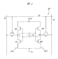
図1は、実施の形態1であるSRAMのメモリセルを示す等価回路図である。図示のように、このメモリセルMCは、一対の相補性データ線(データ線DL、データ線/(バー)DL)とワード線WLとの交差部に配置され、一対の駆動用MISFETQd1,Qd2 、一対の負荷用MISFETQp1,Qp2 および一対の転送用MISFETQt1,Qt2 により構成されている。駆動用MISFETQd1,Qd2 および転送用MISFETQt1,Qt2 はnチャネル型MISFETで構成され、負荷用MISFETQp1,Qp2 はpチャネル型MISFETで構成されている。
【0020】
メモリセルMCを構成する上記6個のMISFETのうち、駆動用MISFETQd1 および負荷用MISFETQp1 は、CMOSインバータINV1 を構成し、駆動用MISFETQd2 および負荷用MISFETQp2 は、CMOSインバータINV2 を構成している。これら一対のCMOSインバータINV1,INV2 の相互の入出力端子(蓄積ノードA、B)は、交差結合され、1ビットの情報を記憶する情報蓄積部としてのフリップフロップ回路を構成している。また、このフリップフロップ回路の一方の入出力端子(蓄積ノードA)は、転送用MISFETQt1 のソース、ドレイン領域の一方に接続され、他方の入出力端子(蓄積ノードB)は、転送用MISFETQt2 のソース、ドレイン領域の一方に接続されている。
【0021】
さらに、転送用MISFETQt1 のソース、ドレイン領域の他方はデータ線DLに接続され、転送用MISFETQt2 のソース、ドレイン領域の他方はデータ線/DLに接続されている。また、フリップフロップ回路の一端(負荷用MISFETQp1,Qp2 の各ソース領域)は電源電圧(Vcc) に接続され、他端(駆動用MISFETQd1,Qd2 の各ソース領域)は接地(基準)電圧(Vss) に接続されている。
【0022】
上記回路の動作を説明すると、一方のCMOSインバータINV1 の蓄積ノードAが高電位(“H" )であるときには、駆動用MISFETQd2 がONになるので、他方のCMOSインバータINV2 の蓄積ノードBが低電位(“L" )になる。従って、駆動用MISFETQd1 がOFFになり、蓄積ノードAの高電位(“H" )が保持される。すなわち、一対のCMOSインバータINV1,INV2 を交差結合させたラッチ回路によって相互の蓄積ノードA、Bの状態が保持され、電源電圧が印加されている間、情報が保存される。
【0023】
転送用MISFETQt1,Qt2 のそれぞれのゲート電極にはワード線WLが接続され、このワード線WLによって転送用MISFETQt1,Qt2 の導通、非導通が制御される。すなわち、ワード線WLが高電位(“H" )であるときには、転送用MISFETQt1,Qt2 がONになり、フリップフロップ回路と相補性データ線(データ線DL,/DL)とが電気的に接続されるので、蓄積ノードA、Bの電位状態(“H" または“L" )がデータ線DL、/DLに現れ、メモリセルMCの情報として読み出される。
【0024】
メモリセルMCに情報を書き込むには、ワード線WLを“H" 電位レベル、転送用MISFETQt1,Qt2 をON状態にしてデータ線DL、/DLの情報を蓄積ノードA、Bに伝達する。この蓄積ノードA、B間に、α線対策のために、容量CSRを付加する。
【0025】
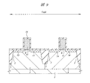
このような、SRAMのメモリセルは、図2に示すメモリセル形成領域(SRAM)に形成され、その周辺には、例えば、論理回路形成領域(Logic)やアナログ容量形成領域(Analog Capacitor)が存在する。後述するように、論理回路形成領域(Logic)には、例えば、論理回路を構成するnチャネルMISFETQnやpチャネル型MISFETQpが形成され、また、アナログ容量形成領域(Analog Capacitor)には、アナログ容量CANが形成される。これらのメモリセル形成領域(SRAM)、論理回路形成領域(Logic)やアナログ容量形成領域(Analog Capacitor)は、単一の半導体基板1上に形成されている。
【0026】
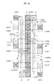
次に、本実施の形態の半導体集積回路装置をその製造工程に従って説明する。図3〜図39は、本実施の形態の半導体集積回路装置の製造方法を示す基板の要部断面図もしくは平面図である。
【0027】
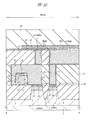
図3〜図6に示すように、まず、半導体基板1中に素子分離2を形成する。ここで、図6は、メモリセル形成領域(SRAM)に形成されるメモリセル約1個分の領域を示す半導体基板の平面図であり、図3の左側の図は、図6のA−A断面図であり、図4は、図6のB−B断面図である。また、図3の右側の図は、アナログ容量形成領域(Analog Capacitor)の断面図であり、図5は、論理回路形成領域(Logic)の断面図である。
【0028】
この素子分離2は、以下のように形成する。例えば1〜10Ωcm程度の比抵抗を有するp型の単結晶シリコンからなる半導体基板1をエッチングすることにより深さ250nm程度の素子分離溝を形成する。
【0029】
その後、例えば半導体基板1を約1000℃で熱酸化することによって、溝の内壁に膜厚10nm程度の薄い酸化シリコン膜(図示せず)からなる絶縁膜を形成する。この酸化シリコン膜は、溝の内壁に生じたドライエッチングのダメージを回復すると共に、次の工程で溝の内部に埋め込まれる酸化シリコン膜5と半導体基板1との界面に生じるストレスを緩和するために形成する。
【0030】
次に、溝の内部を含む半導体基板1上に例えばCVD(Chemical Vapor deposition)法で膜厚450〜500nm程度の酸化シリコン膜5からなる絶縁膜を堆積し、化学的機械研磨(CMP;Chemical Mechanical Polishing)法で溝の上部の酸化シリコン膜5を研磨し、その表面を平坦化する。
【0031】
次に、例えば半導体基板1にp型不純物(ホウ素)およびn型不純物(例えばリン)をイオン打ち込みした後、約1000℃の熱処理で上記不純物を拡散させることによって、半導体基板1にp型ウエル(領域)3およびn型ウエル(領域)4を形成する。
【0032】
その結果、図3の左図、図4および図6に示すように、メモリセル形成領域(SRAM)の半導体基板1には、p型ウエル3およびn型ウエル4主表面である活性領域An1、An2、Ap1、Ap2が形成され、これらの活性領域は、絶縁膜である酸化シリコン膜5が埋め込まれた素子分離2で囲まれている。
【0033】
また、図5に示すように、論理回路形成領域(Logic)の半導体基板1には、p型ウエル3およびn型ウエル4が形成される。
【0034】
また、図3の右側に示すように、アナログ容量形成領域(Analog Capacitor)は、素子分離2で覆われている。
【0035】
追って詳細に説明するように、メモリセル形成領域(SRAM)の半導体基板1の主表面には、メモリセルMCを構成する6個のMISFET(Qt1、Qt2、Qd1、Qd2、Qp1、Qp2)が形成され、このうちnチャネル型MISFET(Qt1、Qd1)は、活性領域Ap1(p型ウエル3)上に形成され、nチャネル型MISFET(Qt2、Qd2)は、活性領域Ap2(p型ウエル3)上に形成される。また、pチャネル型MISFET(Qp2)は、活性領域An1(n型ウエル4)上に形成され、pチャネル型MISFET(Qp1)は、活性領域An2(n型ウエル4)上に形成される(図10参照)。
【0036】
また、論理回路形成領域(Logic)のp型ウエル3には、論理回路を構成するnチャネルMISFETQnが形成され、n型ウエル4には、論理回路を構成するpチャネル型MISFETQpが形成される。
【0037】
次に、例えばフッ酸系の洗浄液を用いて半導体基板1(p型ウエル3およびn型ウエル4)の表面をウェット洗浄した後、図7〜図10に示すように、約800℃の熱酸化でp型ウエル3およびn型ウエル4のそれぞれの表面に膜厚6nm程度の清浄なゲート酸化膜(ゲート絶縁膜)8を形成する。
【0038】
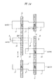
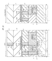
次いで、ゲート酸化膜8上にゲート電極Gを形成する。ここで、図10は、メモリセル形成領域(SRAM)に形成されるメモリセル約1個分の領域を示す半導体基板の平面図であり、図7の左側の図は、図10のA−A断面図であり、図8は、図10のB−B断面図である。また、図7の右側の図は、アナログ容量形成領域(Analog Capacitor)の断面図であり、図9は、論理回路形成領域(Logic)の断面図である。
【0039】
このゲート電極Gは、以下のように形成する。まず、ゲート酸化膜8の上部に例えば膜厚100nm程度の低抵抗多結晶シリコン膜9をCVD法で堆積する。
【0040】
次に、例えばフォトレジスト膜(図示せず)をマスクにして多結晶シリコン膜9をドライエッチングすることにより、多結晶シリコン膜9からなるゲート電極Gを形成する。
【0041】
図10、図7の左図および図8に示すように、メモリセル形成領域(SRAM)の活性領域Ap1上には、転送用MISFETQt1のゲート電極Gと、駆動用MISFETQd1のゲート電極Gが形成され、活性領域Ap2上には、転送用MISFETQt2のゲート電極Gと、駆動用MISFETQd2のゲート電極Gが形成されている。また、活性領域An1上には、負荷用MISFETQp2のゲート電極Gが形成され、活性領域An2上には、負荷用MISFETQp1のゲート電極Gが形成されている。これらのゲート電極は、それぞれ図中のA−Aと直交する方向に形成され、負荷用MISFETQp1のゲート電極Gと駆動用MISFETQd1のゲート電極とは共通であり、また、負荷用MISFETQp2のゲート電極および駆動用MISFETQd2のゲート電極とは共通である。
【0042】
また、論理回路形成領域(Logic)の半導体基板1(p型ウエル3およびn型ウエル4)上にも、このゲート電極Gが形成され(図9)、また、アナログ容量形成領域(Analog Capacitor)の素子分離2上には、配線の役割を果たすゲート電極Gが形成される(図7の左図)。
【0043】
次に、例えばp型ウエル3上のゲート電極Gの両側にn型不純物(リン)を注入することによってn-型半導体領域13を形成し、また、n型ウエル4上にp型不純物(ヒ素)を注入することによってp-型半導体領域14を形成する。
【0044】
次いで、半導体基板1上に例えばCVD法で酸化シリコン膜16堆積する。この酸化シリコン膜は、後述するサイドウォールスペーサ16s形成時のエッチングストッパーとしての機能を有する。
【0045】
さらに、酸化シリコン膜16上に例えばCVD法で窒化シリコン膜からなる絶縁膜を堆積した後、図11〜図14に示すように、異方的にエッチングすることによって、ゲート電極Gの側壁に絶縁膜からなるサイドウォールスペーサ16sを形成する。この際、窒化シリコン膜のエッチングを、その下層の酸化シリコン膜16に対して選択比のとれる条件で行い、半導体基板1(p型ウエル3、n型ウエル4)の表面のエッチングを防止する。次いで、このサイドウォールスペーサ16sをマスクに酸化シリコン膜16をエッチングする。この際、酸化シリコン膜16のエッチングを、その下層の半導体基板1(p型ウエル3、n型ウエル4)に対して選択比のとれる条件で行う。
【0046】
次に、例えばp型ウエル3にn型不純物(リンまたはヒ素)をイオン打ち込みすることによってn+型半導体領域17(ソース、ドレイン)を形成し、n型ウエル4にp型不純物(ホウ素)をイオン打ち込みすることによってp+型半導体領域18(ソース、ドレイン)を形成する。
【0047】
ここで、図14は、メモリセル形成領域(SRAM)に形成されるメモリセル約1個分の領域を示す半導体基板の平面図であり、図11の左側の図は、図14のA−A断面図であり、図12は、図14のB−B断面図である。また、図11の右側の図は、アナログ容量形成領域(Analog Capacitor)の断面図であり、図13は、論理回路形成領域(Logic)の断面図である。
【0048】
ここまでの工程で、メモリセル形成領域(SRAM)に、メモリセルMCを構成する6個のMISFET(駆動用MISFETQd1、Qd2、転送用MISFETQt1、Qt2および負荷用MISFETQp1、Qp2)が完成し、また、論理回路形成領域(Logic)に、nチャネルMISFETQnおよびpチャネル型MISFETQpが完成する。
【0049】
続いて、図15〜図18に示すように、例えば半導体基板1の表面を洗浄した後、半導体基板1上に、スパッタ法により、例えば、Co膜、Ni膜もしくはTi膜等の金属膜を堆積し、次いで、600℃で1分間の熱処理を施すことにより、半導体基板1の露出部(n+型半導体領域17、p+型半導体領域18)およびゲート電極G上に、CoSi2、NiSiもしくはTiSi等の金属シリサイド(シリサイド)層19を形成する。ここで、図18は、メモリセル形成領域(SRAM)に形成されるメモリセル約1個分の領域を示す半導体基板の平面図であり、図15の左側の図は、図18のA−A断面図であり、図16は、図18のB−B断面図である。また、図15の右側の図は、アナログ容量形成領域(Analog Capacitor)の断面図であり、図17は、論理回路形成領域(Logic)の断面図である。
【0050】
次いで、未反応の金属膜をエッチングにより除去した後、700から800℃で、1分間程度の熱処理を施し、金属シリサイド層19を低抵抗化する。
【0051】
次いで、半導体基板1上に例えばCVD法で窒化シリコン膜20からなる絶縁膜を堆積する。なお、この窒化シリコン膜20は、後述するコンタクトホールC1の形成時のエッチングストッパーとしての役割を果たす。
【0052】
続いて、窒化シリコン膜20(絶縁膜)の上部に例えば酸化シリコン膜21からなる絶縁膜を堆積する。この酸化シリコン膜21は、例えば、テトラエトキシシランを原料とし、プラズマCVD法により形成する。この酸化シリコン膜21および窒化シリコン膜20は、ゲート電極Gと後述する局所配線(ローカルインターコネクト)LIとの間の層間絶縁膜となる。
【0053】
次に、図19〜図22に示すように、例えばフォトレジスト膜(図示せず)をマスクにしたドライエッチングで酸化シリコン膜21をドライエッチングし、続いて窒化シリコン膜20をドライエッチングすることによって、コンタクトホールC1を形成する。ここで、図22は、メモリセル形成領域(SRAM)に形成されるメモリセル約1個分の領域を示す半導体基板の平面図であり、図19の左側の図は、図22のA−A断面図であり、図20は、図22のB−B断面図である。また、図19の右側の図は、アナログ容量形成領域(Analog Capacitor)の断面図であり、図21は、論理回路形成領域(Logic)の断面図である。
【0054】
即ち、メモリセル形成領域(SRAM)のn+型半導体領域17(ソース、ドレイン)およびp+型半導体領域18(ソース、ドレイン)上にコンタクトホールC1を形成する。このうち、負荷用MISFETQp1のドレイン上のコンタクトホールC1は、負荷用MISFETQp2のゲート電極上まで延在している。また、負荷用MISFETQp2のドレイン上のコンタクトホールC1は、負荷用MISFETQp1のゲート電極上まで延在している。また、転送用MISFETQt1、Qt2のゲート電極G上にコンタクトホールC1を形成する(図22、図19の左図、図20)。
【0055】
また、論理回路形成領域(Logic)のn+型半導体領域17(ソース、ドレイン)およびp+型半導体領域18(ソース、ドレイン)上にコンタクトホールC1を形成する(図21)。また、アナログ容量形成領域(Analog Capacitor)のゲート電極G(配線)上にコンタクトホールC1を形成する(図19の右図)。
【0056】
次いで、例えばコンタクトホールC1内に導電性膜を埋め込むことによりプラグ(接続部)P1を形成する。このプラグP1を形成するには、まず、コンタクトホールC1の内部を含む酸化シリコン膜21の上部にスパッタ法により例えば、TiN膜よりなる薄いバリア層を堆積し、次いでCVD法により例えば、W(タングステン)膜よりなる導電性膜を堆積する。この後、酸化シリコン膜21の表面が露出するまでエッチバックもしくはCMPを施し、コンタクトホールC1外部のTiN膜およびW膜を除去することにより、コンタクトホールC1内にプラグP1を形成する。
【0057】
次いで、図23〜図26に示すように、プラグP1および酸化シリコン膜21上に、酸化シリコン膜22からなる絶縁膜をCVD法により堆積する。次いで、フォトレジスト膜(図示せず)をマスクにしたドライエッチングで酸化シリコン膜22をドライエッチングすることによって、プラグP1上に配線溝HM0を形成する。
【0058】
ここで、図26は、メモリセル形成領域(SRAM)に形成されるメモリセル約1個分の領域を示す半導体基板の平面図であり、図23の左側の図は、図26のA−A断面図であり、図24は、図26のB−B断面図である。また、図23の右側の図は、アナログ容量形成領域(Analog Capacitor)の断面図であり、図25は、論理回路形成領域(Logic)の断面図である。
【0059】
即ち、メモリセル形成領域(SRAM)のn+型半導体領域17(ソース、ドレイン)およびp+型半導体領域18(ソース、ドレイン)上のプラグP1上に配線溝HM0を形成する。
【0060】
このうち、負荷用MISFETQp1のドレインと接続されるプラグP1上の配線溝HM0は、駆動用MISFETQd1のドレインと接続されるプラグP1上まで延在している。また、負荷用MISFETQp2のドレインと接続されるプラグP1上の配線溝HM0は、駆動用MISFETQd2のドレインと接続されるプラグP1上まで延在している(図26、図23の左図、図24)。これらの配線溝HM0内に形成される局所配線LIc(M0c)は、後述するSRAM容量CSRの下部電極を構成する。また、転送用MISFETQt1、Qt2のゲート電極G上のプラグP1上に配線溝HM0を形成する(図26)。
【0061】
また、論理回路形成領域(Logic)のn+型半導体領域17(ソース、ドレイン)およびp+型半導体領域18(ソース、ドレイン)上のプラグP1上に配線溝HM0を形成する(図25)。さらに、アナログ容量形成領域(Analog Capacitor)のゲート電極G(配線)上のプラグP1上に配線溝HM0を形成する(図23の右図)。このプラグP1上の配線溝HM0内に形成される局所配線LIc(M0c)は、後述するアナログ容量CANの下部電極を構成する。
【0062】
なお、アナログ容量形成領域(Analog Capacitor)においては、酸化シリコン膜21上にも、配線溝HM0が形成されている。この配線溝は、後述するアナログ容量CANの上部電極(24)に所望の電位を印加するための配線を形成するために用いられる。なお、アナログ容量CANの下部電極(LIc(M0c))には、ゲート電極G(配線)を介して所望の電位が印加される。
【0063】
このように、本実施の形態によれば、アナログ容量CANの上部電極(24)に後述する局所配線LI(M0)を介してその裏面より所望の電位を印加するため、上部電極上にコンタクトホール(プラグ)を形成することがなく、コンタクトホール形成時(エッチング時)の上部電極のダメージを防止することができる。
【0064】
次いで、配線溝HM0内に導電性膜を埋め込むことにより局所配線(ローカルインターコネクト)LI、LIcを形成する。この局所配線は、後述する第1層配線より下層に位置する配線であるため、「M0」と、呼ばれることもある。この局所配線(ローカルインターコネクト)LI(M0)、LIc(M0c)を形成するには、まず、配線溝HM0の内部を含む酸化シリコン膜22の上部にスパッタ法により例えば、TiN膜よりなる薄いバリア層を堆積し、次いでCVD法により例えば、W膜よりなる導電性膜を堆積する。この後、酸化シリコン膜22の表面が露出するまでエッチバックもしくはCMPを施し、配線溝HM0外部のTiN膜およびW膜を除去することにより形成する。
【0065】
このように、本実施の形態によれば、配線溝HM0内に導電性膜(TiN膜およびW膜)を埋め込むことにより局所配線LI(M0)、LIc(M0c)を形成したので、その上部が平坦化され、その上部に形成される容量絶縁膜や上部電極を精度良く形成することができる。例えば、隣接する容量間での容量ばらつきを3%以下とすることができ、また、総合ばらつきを20%以下とすることができる。
【0066】
この工程により、メモリセル形成領域(SRAM)においては、負荷用MISFETQp1のドレイン、駆動用MISFETQd1のドレイン、負荷用MISFETQp2のゲート電極が、局所配線LIc(M0c)およびプラグP1を介して接続される。また、負荷用MISFETQp2のドレイン、駆動用MISFETQd2のドレイン、負荷用MISFETQp1のゲート電極が、局所配線LIc(M0c)およびプラグP1を介して接続される。
【0067】
ここで、SRAMのメモリセルアレイ中には、複数のメモリセルが縦、横に反復して形成される。図26の破線は、メモリセルの単位領域を示す。例えば、この矩形状の領域の長辺および短辺に対し、線対称に複数のメモリセルが形成される。
【0068】
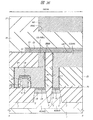
次いで、図27〜図30に示すように、酸化シリコン膜22および局所配線LI(M0)、LIc(M0c)上に例えば、窒化シリコン膜23を形成する。この窒化シリコン膜23は、局所配線LIc(M0c)と後述する上部電極24との間に形成され、容量絶縁膜となる。この窒化シリコン膜23(容量絶縁膜)の膜厚は、例えば、メモリセルの1個分の領域(単位領域)が2.0μm2であって、前述の一つの局所配線LIc(M0c)の形成領域が0.17μm2の場合には、10nm程度とする。
【0069】
ここで、図30は、メモリセル形成領域(SRAM)に形成されるメモリセル約1個分の領域を示す半導体基板の平面図であり、図27の左側の図は、図30のA−A断面図であり、図28は、図30のB−B断面図である。また、図27の右側の図は、アナログ容量形成領域(Analog Capacitor)の断面図であり、図29は、論理回路形成領域(Logic)の断面図である。
【0070】
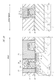
次に、メモリセル形成領域(SRAM)に形成された2つの容量を構成する局所配線LIc(M0c)のうち、いずれか一方の局所配線LIc(M0c)上の窒化シリコン膜23を除去し、開口部OP1を形成する(図30、図28)。また、アナログ容量形成領域(Analog Capacitor)に形成された局所配線LI(M0)上の窒化シリコン膜23を除去し、開口部OP2を形成する(図27)。
【0071】
次いで、開口部OP1、OP2内を含む窒化シリコン膜23上に、スパッタ法によりTiN膜もしくはW膜のような導電性膜を堆積し、パターニングすることによって、前記局所配線LIc(M0c)上に、上部電極24を形成する。
【0072】
ここで、メモリセル形成領域(SRAM)の上部電極24は、2つの局所配線LIc(M0c)を覆うよう形成され、さらに、この上部電極24は、開口部OP1を介して局所配線LIc(M0c)と接続される(図30、図27の左図、図28)。また、同様に、アナログ容量形成領域(Analog Capacitor)の上部電極24は、容量を構成する局所配線LIc(M0c)を覆うよう形成され、さらに、この上部電極24は、開口部OP2を介して局所配線LI(M0)と接続される(図27の左図)。
【0073】
このように、本実施の形態によれば、上部電極24は、局所配線LIc(M0c)を覆うようパターニングされるため、上部電極24の形成時(W膜のエッチング時)に、局所配線LIc(M0c)上の容量絶縁膜23、即ち、容量に寄与する容量絶縁膜がエッチングされることがなく、容量端部でのリーク電流を防止することができる。また、前述の局所配線LIcの端部は、プラグ(接続部)P1の上部に形成される。
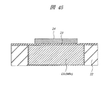
【0074】
例えば、図45に示すように、上部電極24によって覆われない局所配線LIc(M0c)の部分が存在する場合には、上部電極24の形成時(W膜のエッチング時)に、上部電極24端部において、容量絶縁膜23がダメージを受け、また、オーバーエッチングされた場合には、その膜厚が減少する。その結果、容量絶縁膜中のピンホールが発生し、リーク電流が増加してしまう。これに対して、本実施の形態では、容量に寄与する容量絶縁膜がエッチングされることがないので、リーク電流を防止することができる。
【0075】
特に、窒化シリコン膜とTiN膜は、エッチングレートの差が小さいため、選択比がとりにくく、上部電極24にTiN膜を用い、また、容量絶縁膜23に窒化シリコン膜を用いる場合に、適用して効果が大きい。
【0076】
以上の工程により、メモリセル形成領域(SRAM)に、局所配線LIc(M0c)と、窒化シリコン膜23と上部電極24とで構成されるSRAM容量CSRを形成することができ、また、アナログ容量形成領域(Analog Capacitor)に、局所配線LIc(M0c)と、窒化シリコン膜23と上部電極24とで構成されるアナログ容量CANを形成することができる。
【0077】
このように、本実施の形態によれば、メモリセル形成領域に形成されるSRAMの蓄積ノード間(局所配線上)に、SRAM容量CSRを形成したので、SRAMのメモリセルに入射したα線によるソフトエラーを低減することができる。
【0078】
また、本実施の形態によれば、SRAM容量CSRとアナログ容量CANを同一工程で形成することができる。
【0079】
この際、前述した通り、下部電極となる局所配線LIc(M0c)上が平坦化されているので、SRAM容量CSRやアナログ容量CANの容量ばらつきを低減することができる。また、前述したように、アナログ容量CANに要求される、3%以下の隣接間容量ばらつき、および20%以下の総合ばらつきを達成することができる。
【0080】
さらに、本実施の形態においては、SRAM容量CSRとアナログ容量CANの下部電極(局所配線)や上部電極をW膜等の金属膜やTiN膜等の導電性を有する金属の化合物膜で構成(いわゆるMIM(Metal Insulator Metal)構造)したので、容量特性を向上させることができる。例えば、これらの電極材料としてポリシリコンを用いた場合には、ポリシリコン内に空乏層が生じ得るため、電圧依存性が生じてしまう。これに比べMIM構造においては、電圧依存性を抑えることができる。
【0081】
また、アナログ容量CANは、酸化シリコン膜21上に形成されるため、基板電位の影響を受けにくく、容量の電圧特性を向上させることができる。
【0082】
また、容量絶縁膜の膜厚が、ゲート絶縁膜の膜厚と無関係に設定できるので、トンネル電流によるリーク電流を防止することができる。なお、トンネル電流は、絶縁膜の膜厚が2.6nm未満の場合に1×10⁻⁴A/cm2を越えるので、容量絶縁膜の膜厚を2.6nm以上とする必要がある。
【0083】
この後、上部電極24上に層間絶縁膜(酸化シリコン膜25)を介し第1層配線M1および第2層配線M2が形成される。引き続き、これらの配線の形成工程について説明する。
【0084】
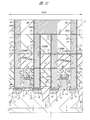
まず、図31〜図34に示すように、上部電極24上および窒化シリコン膜23に、酸化シリコン膜25をCVD法により堆積する。次いで、局所配線LI(M0)、LIc(M0c)上の酸化シリコン膜25および窒化シリコン膜23をエッチングにより除去することによりコンタクトホールC2を形成する。ここで、図34は、メモリセル形成領域(SRAM)に形成されるメモリセル約1個分の領域を示す半導体基板の平面図であり、図31の左側の図は、図34のA−A断面図であり、図32は、図34のB−B断面図である。また、図31の右側の図は、アナログ容量形成領域(Analog Capacitor)の断面図であり、図33は、論理回路形成領域(Logic)の断面図である。
【0085】
即ち、メモリセル形成領域(SRAM)の局所配線LI(M0)、LIc(M0c)上にコンタクトホールC2を形成する(図34)。このうち、転送用MISFETQt1、Qt2のゲート電極Gと接続される局所配線LI(M0)上のコンタクトホールC2は、第1層配線M1(ワード線WL)と前記ゲート電極Gとの接続のために用いられる。
【0086】
また、アナログ容量形成領域(Analog Capacitor)においては、局所配線LI(M0)上であって、図31に示す断面には現れない領域上に、コンタクトホールC2が形成される。このコンタクトホールC2は、アナログ容量CANの上部電極24に、局所配線LI(M0)を介して所望の電位を印加するために用いられる。
【0087】
さらに、論理回路形成領域(Logic)の局所配線LI(M0)上にコンタクトホールC2を形成する(図33)。
【0088】
次いで、コンタクトホールC2内に導電性膜を埋め込むことによりプラグP2を形成する。このプラグP2を形成するには、まず、コンタクトホールC2の内部を含む酸化シリコン膜25の上部にスパッタ法により例えば、TiN膜よりなる薄いバリア層を堆積し、次いでCVD法により例えば、W膜よりなる導電性膜を堆積する。この後、酸化シリコン膜25の表面が露出するまでエッチバックもしくはCMPを施し、コンタクトホールC2外部のTiN膜およびW膜を除去する。
【0089】
続いて、図35〜図38に示すように、酸化シリコン膜25およびプラグP2上に、第1層配線M1およびプラグP3を形成する。この第1層配線M1およびプラグP3は、例えば、銅膜よりなる埋め込み配線および埋め込みプラグとすることができる。ここで、図38は、メモリセル形成領域(SRAM)に形成されるメモリセル約1個分の領域を示す半導体基板の平面図であり、図35の左側の図は、図38のA−A断面図であり、図36は、図38のB−B断面図である。また、図35の右側の図は、アナログ容量形成領域(Analog Capacitor)の断面図であり、図37は、論理回路形成領域(Logic)の断面図である。
【0090】
この第1層配線M1およびプラグP3を形成するには、まず、酸化シリコン膜25およびプラグP2上に、酸化シリコン膜27をCVD法により堆積し、次いで、フォトレジスト膜(図示せず)をマスクにしたドライエッチングで酸化シリコン膜27をドライエッチングすることによって、配線溝HM1およびコンタクトホールC3を形成する。次に、配線溝HM1およびコンタクトホールC3内を含む酸化シリコン膜25に例えば、TiN膜からなる薄いバリア層をスパッタ法もしくはCVD法により堆積し、次いで、このバリア層上に、銅(Cu)膜をスパッタ法もしくはメッキ法により形成する。この後、酸化シリコン膜27の表面が露出するまでエッチバックもしくはCMPを施し、配線溝HM1およびコンタクトホールC3外部のTiN膜およびCu膜を除去することにより、配線溝HM1内に第1層配線M1を、また、コンタクトホールC3内にプラグP3を形成する。
【0091】
即ち、メモリセル形成領域(SRAM)には、転送用MISFETQt1のゲート電極Gと電気的に接続されるプラグP2と、転送用MISFETQt2のゲート電極Gと電気的に接続されるプラグP2とを接続するよう第1層配線M1(ワード線WL)を形成する。また、前記プラグP2以外のプラグP2上には、プラグP3が形成される(図38)。
【0092】
また、論理回路形成領域(Logic)のプラグP2上にも、第1層配線M1等が形成される(図37)。また、図38中には現れないが、アナログ容量形成領域(Analog Capacitor)のプラグP2上にも、第1層配線M1等が形成される。
【0093】
次いで、図39に示すように、第1層配線M1、プラグP3および酸化シリコン膜27上に、酸化シリコン膜をCVD法により堆積し、この酸化シリコン膜中に、コンタクトホールC2およびプラグP2と同様に、コンタクトホールC4およびプラグP4を形成する。ここで、図39は、メモリセル形成領域(SRAM)に形成されるメモリセル約1個分の領域を示す半導体基板の平面図である。
【0094】
続いて、前記酸化シリコン膜およびプラグP4上に、酸化シリコン膜をCVD法により堆積し、この膜中に、第1層配線M1と同様に、第2層配線M2を形成する。この第2層配線M2および前述のプラグP4は、メモリセル形成領域(SRAM)、アナログ容量形成領域(Analog Capacitor)および論理回路形成領域(Logic)の断面図において省略する。なお、メモリセル形成領域(SRAM)においては、図39に示すように、第2層配線M2は、駆動用MISFETQd1ソースと電気的に接続されるプラグP4および駆動用MISFETQd2のソースと電気的に接続されるプラグP4上に、これらを接続するよう形成され、かかる第2層配線M2には、接地電圧(Vss)が印加される。また、第2層配線M2は、負荷用MISFETQp1ソースと電気的に接続されるプラグP4および負荷用MISFETQp2のソースと電気的に接続されるプラグP4上に、それぞれ第1層配線(ワード線WL)と直交する方向に形成され、かかる第2層配線M2には、電源電圧(Vcc)が印加される。さらに、第2層配線M2は、転送用MISFETQt1およびQt2の一端と電気的に接続されるプラグP4上に、それぞれ第1層配線(ワード線WL)と直交する方向に形成され、かかる第2層配線M2は、データ線対DL、/DL(ビット線対)となる。
【0095】
以上の工程により、図1及び図2を用いて説明したSRAMメモリセル、論理回路およびアナログ容量を有する半導体集積回路装置が、ほぼ完成する。
【0096】
ここで、本実施の形態において説明したアナログ容量を有する回路についての一例を述べる。
【0097】
図40は、PLL回路の構成を示す図である。このようなPLL回路は、位相比較器401、低域フィルタ402およびVCO(VoltageControledOscillator)403を有し、リファレンスクロックRCに応答して、出力信号を発振させる。この低域フィルタ402には、アナログ容量CANが用いられている。このようなPLL回路を構成するアナログ容量CANを、前述したように、ゲート絶縁膜を用いて形成した場合は、トンネル電流によるリーク電流が問題となる。このリーク電流が、その目標値である1×10⁻⁴A/cm2を超えるような場合は、時間誤差が生じ、PLL回路の正常動作を阻害してしまう。
【0098】
しかしながら、本実施の形態で説明したアナログ容量CANを用いた場合は、前述したように容量絶縁膜の膜厚を確保することができ、PLL回路のリーク電流を低減でき、PLL回路の誤動作を防止することができる。
【0099】
なお、本実施の形態で説明したアナログ容量CANは、前述のPLL回路に限られず、広く容量を有する回路に適用可能である。
【0100】
(実施の形態2)
次に、本実施の形態の半導体集積回路装置をその製造工程に従って説明する。図41〜図44は、本実施の形態の半導体集積回路装置の製造方法を示す基板の要部断面図もしくは平面図である。なお、図2〜図26を用いて説明した局所配線LI(M0)、LIc(M0c)の形成工程までは、実施の形態1の場合と同様であるためその説明を省略する。
【0101】
まず、実施の形態1で説明した図23〜図26に示す半導体基板1を準備する。これらの図中の局所配線LI(M0)、LIc(M0c)は、実施の形態1で説明した通り、酸化シリコン膜22中に形成された配線溝HM0内部を含む酸化シリコン膜22の上部にスパッタ法により例えば、TiN膜よりなる薄いバリア層を堆積し、次いでCVD法により例えば、W膜よりなる導電性膜を堆積した後、酸化シリコン膜22の表面が露出するまでエッチバックもしくはCMPを施すことにより形成する。
【0102】
本実施の形態においては、図41〜図44に示すように、この酸化シリコン膜22の表面をさらに100nm程度エッチングし、局所配線LI(M0)、LIc(M0c)の側壁上部を露出させる。ここで、図44は、メモリセル形成領域(SRAM)に形成されるメモリセル約1個分の領域を示す半導体基板の平面図であり、図41の左側の図は、図44のA−A断面図であり、図42は、図44のB−B断面図である。また、図41の右側の図は、アナログ容量形成領域(Analog Capacitor)の断面図であり、図43は、論理回路形成領域(Logic)の断面図である。
【0103】
次いで、酸化シリコン膜22および局所配線LI(M0)、LIc(M0c)上に例えば、窒化シリコン膜23を形成する。この窒化シリコン膜23は、局所配線LIc(M0c)と後述する上部電極24との間に形成され、容量絶縁膜となる。この窒化シリコン膜23(容量絶縁膜)の膜厚は、例えば、メモリセル約1個分の領域が2.0μm2の場合には、20nm程度とする。
【0104】
次に、メモリセル形成領域(SRAM)に形成された2つの局所配線LIc(M0c)のうち、いずれか一方の局所配線LIc(M0c)上の窒化シリコン膜23を除去し、開口部OP1を形成する(図34、図32)。また、アナログ容量形成領域(Analog Capacitor)に形成された局所配線LI(M0)上の窒化シリコン膜23を除去し、開口部OP2を形成する(図31)。
【0105】
次いで、実施の形態1の場合と同様に、開口部OP1、OP2内を含む窒化シリコン膜23上に、スパッタ法により例えば、TiN膜もしくはW膜を堆積し、パターニングすることによって、前記局所配線LIc(M0c)上に、上部電極24を形成する。
【0106】
以上の工程により、メモリセル形成領域(SRAM)に、局所配線LIc(M0c)と、窒化シリコン膜23と上部電極24とで構成されるSRAM容量CSRを形成することができ、また、アナログ容量形成領域(Analog Capacitor)に、局所配線LIc(M0c)と、窒化シリコン膜23と上部電極24とで構成されるアナログ容量CANを形成することができる。
【0107】
以降の工程は、図31〜図39を参照しながら説明した実施の形態1の場合と同様であるため、その説明を省略する。
【0108】
このように、本実施の形態によれば、実施の形態1で説明した効果に加え、局所配線LIc(M0c)を形成した後、酸化シリコン膜22の表面をさらに、エッチングしたので、局所配線LIc(M0c)の側壁上部が露出し、この側壁に沿って容量絶縁膜となる窒化シリコン膜23を形成することができるため、容量を増加させることができる。
【0109】
以上、本発明者によってなされた発明を実施の形態に基づき具体的に説明したが、本発明は前記実施の形態に限定されるものではなく、その要旨を逸脱しない範囲で種々変更可能であることはいうまでもない。
【0110】
【発明の効果】
本願において開示される発明のうち、代表的なものによって得られる効果を簡単に説明すれば以下のとおりである。
【0111】
SRAMのメモリセルの蓄積ノード間に容量を形成することにより、ソフトエラーを低減させることができる。
【0112】
また、かかる容量と、アナログ容量を有する素子とを単一の基板上に形成することができ、これらの容量によるリーク電流の低減を図ることができる。また、これらの容量の電圧依存性を低減することがきる。また、これらの容量のばらつきを低減することがきる。
【0113】
その結果、これらの容量を有する半導体集積回路装置の性能を向上させることができる。
【図面の簡単な説明】
【図1】本発明の実施の形態1である半導体集積回路装置中のSRAMのメモリセルを示す等価回路図である。
【図2】本発明の実施の形態1である半導体集積回路装置の製造方法を示す基板の要部平面図である。
【図3】本発明の実施の形態1である半導体集積回路装置の製造方法を示す基板の要部断面図である。
【図4】本発明の実施の形態1である半導体集積回路装置の製造方法を示す基板の要部断面図である。
【図5】本発明の実施の形態1である半導体集積回路装置の製造方法を示す基板の要部断面図である。
【図6】本発明の実施の形態1である半導体集積回路装置の製造方法を示す基板の要部平面図である。
【図7】本発明の実施の形態1である半導体集積回路装置の製造方法を示す基板の要部断面図である。
【図8】本発明の実施の形態1である半導体集積回路装置の製造方法を示す基板の要部断面図である。
【図9】本発明の実施の形態1である半導体集積回路装置の製造方法を示す基板の要部断面図である。
【図10】本発明の実施の形態1である半導体集積回路装置の製造方法を示す基板の要部平面図である。
【図11】本発明の実施の形態1である半導体集積回路装置の製造方法を示す基板の要部断面図である。
【図12】本発明の実施の形態1である半導体集積回路装置の製造方法を示す基板の要部断面図である。
【図13】本発明の実施の形態1である半導体集積回路装置の製造方法を示す基板の要部断面図である。
【図14】本発明の実施の形態1である半導体集積回路装置の製造方法を示す基板の要部平面図である。
【図15】本発明の実施の形態1である半導体集積回路装置の製造方法を示す基板の要部断面図である。
【図16】本発明の実施の形態1である半導体集積回路装置の製造方法を示す基板の要部断面図である。
【図17】本発明の実施の形態1である半導体集積回路装置の製造方法を示す基板の要部断面図である。
【図18】本発明の実施の形態1である半導体集積回路装置の製造方法を示す基板の要部平面図である。
【図19】本発明の実施の形態1である半導体集積回路装置の製造方法を示す基板の要部断面図である。
【図20】本発明の実施の形態1である半導体集積回路装置の製造方法を示す基板の要部断面図である。
【図21】本発明の実施の形態1である半導体集積回路装置の製造方法を示す基板の要部断面図である。
【図22】本発明の実施の形態1である半導体集積回路装置の製造方法を示す基板の要部平面図である。
【図23】本発明の実施の形態1である半導体集積回路装置の製造方法を示す基板の要部断面図である。
【図24】本発明の実施の形態1である半導体集積回路装置の製造方法を示す基板の要部断面図である。
【図25】本発明の実施の形態1である半導体集積回路装置の製造方法を示す基板の要部断面図である。
【図26】本発明の実施の形態1である半導体集積回路装置の製造方法を示す基板の要部平面図である。
【図27】本発明の実施の形態1である半導体集積回路装置の製造方法を示す基板の要部断面図である。
【図28】本発明の実施の形態1である半導体集積回路装置の製造方法を示す基板の要部断面図である。
【図29】本発明の実施の形態1である半導体集積回路装置の製造方法を示す基板の要部断面図である。
【図30】本発明の実施の形態1である半導体集積回路装置の製造方法を示す基板の要部平面図である。
【図31】本発明の実施の形態1である半導体集積回路装置の製造方法を示す基板の要部断面図である。
【図32】本発明の実施の形態1である半導体集積回路装置の製造方法を示す基板の要部断面図である。
【図33】本発明の実施の形態1である半導体集積回路装置の製造方法を示す基板の要部断面図である。
【図34】本発明の実施の形態1である半導体集積回路装置の製造方法を示す基板の要部平面図である。
【図35】本発明の実施の形態1である半導体集積回路装置の製造方法を示す基板の要部断面図である。
【図36】本発明の実施の形態1である半導体集積回路装置の製造方法を示す基板の要部断面図である。
【図37】本発明の実施の形態1である半導体集積回路装置の製造方法を示す基板の要部断面図である。
【図38】本発明の実施の形態1である半導体集積回路装置の製造方法を示す基板の要部平面図である。
【図39】本発明の実施の形態1である半導体集積回路装置の製造方法を示す基板の要部平面図である。
【図40】本発明の実施の形態1である半導体集積回路装置中に用いられる回路の一例を示す図である。
【図41】本発明の実施の形態2である半導体集積回路装置の製造方法を示す基板の要部断面図である。
【図42】本発明の実施の形態2である半導体集積回路装置の製造方法を示す基板の要部断面図である。
【図43】本発明の実施の形態2である半導体集積回路装置の製造方法を示す基板の要部断面図である。
【図44】本発明の実施の形態2である半導体集積回路装置の製造方法を示す基板の要部平面図である。
【図45】本発明の実施の形態1の効果を説明するための図である。
【符号の説明】
1 半導体基板
2 素子分離
3 p型ウエル
4 n型ウエル
5 酸化シリコン膜
8 ゲート酸化膜
9 多結晶シリコン膜
13 n-型半導体領域
14 p-型半導体領域
16 酸化シリコン膜
16s サイドウォールスペーサ
17 n+型半導体領域
18 p+型半導体領域
19 金属シリサイド層
20 窒化シリコン膜
21 酸化シリコン膜
22 酸化シリコン膜
23 窒化シリコン膜(容量絶縁膜)
24 上部電極
25 酸化シリコン膜
27 酸化シリコン膜
A 蓄積ノード
B 蓄積ノード
An1 活性領域
An2 活性領域
Ap1 活性領域
Ap2 活性領域
CSR SRAM容量
CAN アナログ容量
C1 コンタクトホール
C2 コンタクトホール
C3 コンタクトホール
C4 コンタクトホール
DL、/DL データ線
G ゲート電極
HM0、HM1 配線溝
INV1 CMOSインバータ
INV2 CMOSインバータ
LI(M0) 局所配線
LIc(M0c) 局所配線
M1 第1層配線
M2 第2層配線
MC メモリセル
OP1 開口部
OP2 開口部
P1 プラグ
P2 プラグ
P3 プラグ
P4 プラグ
Qd1 駆動用MISFET
Qd2 駆動用MISFET
Qp1 負荷用MISFET
Qp2 負荷用MISFET
Qt1 転送用MISFET
Qt2 転送用MISFET
WL ワード線
Vcc 電源電圧
Vss 接地電圧
401 位相比較器
402 低域フィルタ
403 VCO
Qn nチャネル型MISFET
Qp pチャネル型MISFET
SRAM メモリセル形成領域
Logic 論理回路形成領域
Analog Capacitor アナログ容量形成領域[0001]
BACKGROUND OF THE INVENTION
The present invention relates to a semiconductor integrated circuit device. In place In particular, the present invention relates to a technique that is effective when applied to a semiconductor integrated circuit device having an SRAM (Static Random Access Memory).
[0002]
[Prior art]
SRAM is used as a cache memory for personal computers and workstations.
[0003]
This SRAM is composed of a flip-flop circuit that stores 1-bit information and two MISFETs (Metal Insulator Semiconductor Field Effect Transistors) for information transfer. This flip-flop circuit is, for example, a pair of driving MISFETs and a pair of MISFETs. MISFET for load.
[0004]
For such a memory cell, a soft error due to α rays is a problem. Soft error caused by alpha rays means that alpha rays contained in external cosmic rays and alpha rays emitted from radioactive atoms contained in LSI packaging materials enter the memory cell and are stored in the memory cell. It is a phenomenon that destroys information.
[0005]
As a countermeasure against this α-ray, a method of adding a capacity to the information storage section (input / output section of the flip-flop circuit) in the memory cell and increasing the capacity of the information storage section has been studied. Such a capacity of the information storage unit is described in, for example, IEDM 1988 P205.
[0006]
[Problems to be solved by the invention]
In particular, the memory cell area tends to be reduced in accordance with recent high integration and miniaturization of semiconductor integrated circuits. As a result, the distance between the information storage unit, that is, the pair of driving n-channel MISFETs and the pair of load p-channel MISFETs is reduced, and is easily affected by α rays. In addition, the power supply voltage (Vcc) tends to decrease due to a reduction in power consumption, and this also increases the incidence of soft errors due to α rays.
[0007]
On the other hand, a so-called system LSI (Large Scale Integrated Circuit) in which the SRAM as described above and, for example, a PLL (Phase Locked Loop) circuit having an analog capacitor is formed on a single substrate has been studied.
[0008]
The analog capacitor used in the PLL circuit includes, for example, a semiconductor substrate (diffusion layer) as a lower electrode, a gate insulating film formed on the semiconductor substrate as a capacitive insulating film, and a conductive film on the gate insulating film. A capacitor having an upper electrode (for example, a polysilicon film) is used.
[0009]
However, in such a capacitor, a tunnel current is generated as the gate insulating film becomes thinner. As a result, the leakage current increases. For example, after the 0.13 μm generation, the leakage current is 1 × 10 which is the target value. -Four A / cm 2 Exceeds the threshold value, and the normal operation of the PLL circuit is hindered.
[0010]
In addition, when a capacitor is formed on a semiconductor substrate, the voltage characteristic of the capacitor changes due to the influence of the substrate potential.
[0011]
An object of the present invention is to provide a semiconductor integrated circuit device, for example, a high-performance semiconductor integrated circuit device in which soft errors in SRAM memory cells are reduced.
[0012]
Another object of the present invention is to improve the performance of a semiconductor integrated circuit device, for example, a system LSI in which an SRAM and an element having an analog capacitor are formed on a single substrate.
[0013]
The above object and novel features of the present invention will become apparent from the description of the present specification and the accompanying drawings.
[0014]
[Means for Solving the Problems]
Of the inventions disclosed in the present application, the outline of typical ones will be briefly described as follows.
[0015]
(1) A semiconductor integrated circuit device according to the present invention includes a pair of conductive layers that electrically connect gate electrodes and drains of a pair of n-channel MISFETs constituting a memory cell, and the pair of conductive layers on the pair of conductive layers. A capacitive insulating film formed, the capacitive insulating film having an opening on one of the pair of conductive layers, and the upper electrode formed on the capacitive insulating film and the opening; Have The pair of conductive layers may be formed in the interlayer insulating film. Further, the upper portion of the conductive layer may protrude from the surface of the interlayer insulating film. In addition, the upper electrode may be formed so that a region where the upper electrode is formed is wider than a region where the conductive layer is formed and includes the region where the conductive layer is formed.
[0016]
(2) In addition to the first region in which the memory cell is formed, a second region is provided, and in this second region, the conductive layer, the capacitive insulating film, and the upper electrode formed in the first region; Other capacitors each formed of the same layer may be formed.
[0017]
(3) In the method of manufacturing a semiconductor integrated circuit device according to the present invention, a wiring trench is formed in an interlayer insulating film on a pair of n-channel MISFETs constituting a memory cell, and a conductive film is embedded, thereby a step of forming a pair of conductive layers electrically connecting each gate electrode and drain of the n-channel MISFET, a step of forming a capacitive insulating film on the pair of conductive layers, and the pair of conductive layers Forming an opening by selectively removing a capacitor insulating film on one of the conductive layers, and depositing and etching a conductive film on the capacitor insulating film including the inside of the opening Forming an upper electrode. Further, after the pair of conductive layers is formed, the sidewalls of the pair of conductive layers may be exposed by etching a surface in the interlayer insulating film. In addition to the first region where the memory cell is formed, a second region is provided, and another capacitor is formed in the second region in the same process as the pair of conductive layers, the capacitor insulating film, and the upper electrode. May be.
[0018]
DETAILED DESCRIPTION OF THE INVENTION
Hereinafter, embodiments of the present invention will be described in detail with reference to the drawings. Note that components having the same function are denoted by the same reference symbols throughout the drawings for describing the embodiments, and the repetitive description thereof will be omitted.
[0019]
(Embodiment 1)
FIG. 1 is an equivalent circuit diagram showing an SRAM memory cell according to the first embodiment. As shown in the figure, this memory cell MC is arranged at the intersection of a pair of complementary data lines (data line DL, data line / (bar) DL) and a word line WL, and a pair of driving MISFETs Qd1, Qd2,. It is composed of a pair of load MISFETs Qp1, Qp2 and a pair of transfer MISFETs Qt1, Qt2. The drive MISFETs Qd1 and Qd2 and the transfer MISFETs Qt1 and Qt2 are configured by n-channel MISFETs, and the load MISFETs Qp1 and Qp2 are configured by p-channel MISFETs.
[0020]
Of the six MISFETs constituting the memory cell MC, the driving MISFET Qd1 and the load MISFET Qp1 constitute a CMOS inverter INV1, and the driving MISFET Qd2 and the load MISFET Qp2 constitute a CMOS inverter INV2. The mutual input / output terminals (storage nodes A and B) of the pair of CMOS inverters INV1 and INV2 are cross-coupled to form a flip-flop circuit as an information storage unit for storing 1-bit information. One input / output terminal (storage node A) of the flip-flop circuit is connected to one of the source and drain regions of the transfer MISFET Qt1, and the other input / output terminal (storage node B) is the source of the transfer MISFET Qt2. , Connected to one of the drain regions.
[0021]
Further, the other of the source and drain regions of the transfer MISFET Qt1 is connected to the data line DL, and the other of the source and drain regions of the transfer MISFET Qt2 is connected to the data line / DL. Further, one end (the source regions of the load MISFETs Qp1, Qp2) of the flip-flop circuit is connected to the power supply voltage (Vcc), and the other end (the source regions of the drive MISFETs Qd1, Qd2) is connected to the ground (reference) voltage (Vss). It is connected to the.
[0022]
Explaining the operation of the above circuit, when the storage node A of one CMOS inverter INV1 is at a high potential ("H"), the driving MISFET Qd2 is turned on, so that the storage node B of the other CMOS inverter INV2 is at a low potential. ("L"). Accordingly, the driving MISFET Qd1 is turned OFF, and the high potential (“H”) of the storage node A is held. That is, the state of the mutual storage nodes A and B is held by a latch circuit in which a pair of CMOS inverters INV1 and INV2 are cross-coupled, and information is stored while the power supply voltage is applied.
[0023]
A word line WL is connected to each gate electrode of the transfer MISFETs Qt1 and Qt2, and conduction and non-conduction of the transfer MISFETs Qt1 and Qt2 are controlled by the word line WL. That is, when the word line WL is at a high potential ("H"), the transfer MISFETs Qt1 and Qt2 are turned on, and the flip-flop circuit and the complementary data lines (data lines DL and / DL) are electrically connected. Therefore, the potential state (“H” or “L”) of the storage nodes A and B appears on the data lines DL and / DL and is read as information of the memory cell MC.
[0024]
In order to write information in the memory cell MC, the word line WL is set to the “H” potential level, the transfer MISFETs Qt1 and Qt2 are turned on, and the information on the data lines DL and / DL is transmitted to the storage nodes A and B. Between the storage nodes A and B, a capacitor C is used to prevent α rays. SR Is added.
[0025]
Such SRAM memory cells are formed in the memory cell formation region (SRAM) shown in FIG. 2, and there are, for example, a logic circuit formation region (Logic) and an analog capacitance formation region (Analog Capacitor) in the periphery. To do. As will be described later, in the logic circuit formation region (Logic), for example, an n-channel MISFET Qn and a p-channel MISFET Qp constituting the logic circuit are formed, and in the analog capacitor formation region (Analog Capacitor), an analog capacitor C AN Is formed. These memory cell formation region (SRAM), logic circuit formation region (Logic), and analog capacitance formation region (Analog Capacitor) are formed on a single semiconductor substrate 1.
[0026]
Next, the semiconductor integrated circuit device of the present embodiment will be described according to the manufacturing process. 3 to 39 are cross-sectional views or plan views of main parts of the substrate showing the method of manufacturing the semiconductor integrated circuit device of the present embodiment.
[0027]
As shown in FIGS. 3 to 6, first,
[0028]
This
[0029]
Thereafter, for example, the semiconductor substrate 1 is thermally oxidized at about 1000 ° C. to form an insulating film made of a thin silicon oxide film (not shown) having a thickness of about 10 nm on the inner wall of the groove. This silicon oxide film recovers damage caused by dry etching that has occurred on the inner wall of the groove, and also relieves stress generated at the interface between the
[0030]
Next, an insulating film made of a
[0031]
Next, for example, after p-type impurities (boron) and n-type impurities (for example, phosphorus) are ion-implanted into the semiconductor substrate 1, the impurities are diffused by a heat treatment at about 1000 ° C., so that the p-type well ( Region) 3 and n-type well (region) 4 are formed.
[0032]
As a result, as shown in the left diagram of FIG. 3, FIGS. 4 and 6, the semiconductor substrate 1 in the memory cell formation region (SRAM) has an active region An1, which is the main surface of the p-
[0033]
In addition, as shown in FIG. 5, a p-
[0034]
As shown on the right side of FIG. 3, the analog capacitor formation region (Analog Capacitor) is covered with the
[0035]
As will be described in detail later, six MISFETs (Qt1, Qt2, Qd1, Qd2, Qp1, Qp2) constituting the memory cell MC are formed on the main surface of the semiconductor substrate 1 in the memory cell formation region (SRAM). Of these, the n-channel MISFETs (Qt1, Qd1) are formed on the active region Ap1 (p-type well 3), and the n-channel MISFETs (Qt2, Qd2) are formed on the active region Ap2 (p-type well 3). Formed. The p-channel type MISFET (Qp2) is formed on the active region An1 (n-type well 4), and the p-channel type MISFET (Qp1) is formed on the active region An2 (n-type well 4) (FIG. 10).
[0036]
Further, an n-channel MISFET Qn constituting a logic circuit is formed in the p-type well 3 in the logic circuit formation region (Logic), and a p-channel MISFET Qp constituting a logic circuit is formed in the n-
[0037]
Next, the surface of the semiconductor substrate 1 (p-
[0038]
Next, a gate electrode G is formed on the
[0039]
The gate electrode G is formed as follows. First, a low-resistance
[0040]
Next, the
[0041]
As shown in the left diagram of FIG. 10, FIG. 7 and FIG. 8, the gate electrode G of the transfer MISFET Qt1 and the gate electrode G of the drive MISFET Qd1 are formed on the active region Ap1 of the memory cell formation region (SRAM). The gate electrode G of the transfer MISFET Qt2 and the gate electrode G of the drive MISFET Qd2 are formed on the active region Ap2. Further, the gate electrode G of the load MISFET Qp2 is formed on the active region An1, and the gate electrode G of the load MISFET Qp1 is formed on the active region An2. These gate electrodes are respectively formed in a direction orthogonal to AA in the figure, the gate electrode G of the load MISFET Qp1 and the gate electrode of the drive MISFET Qd1 are common, and the gate electrode of the load MISFET Qp2 and The gate electrode of the driving MISFET Qd2 is common.
[0042]
Further, the gate electrode G is also formed on the semiconductor substrate 1 (p-
[0043]
Next, for example, n-type impurities (phosphorus) are implanted on both sides of the gate electrode G on the p-type well 3 to make n - P-
[0044]
Next, a
[0045]
Further, an insulating film made of a silicon nitride film is deposited on the
[0046]
Next, for example, n-type impurities (phosphorus or arsenic) are ion-implanted into the p-type well 3 to form n + Type semiconductor region 17 (source, drain) is formed, and p-type impurity (boron) is ion-implanted into n-type well 4 to form p + A type semiconductor region 18 (source, drain) is formed.
[0047]
Here, FIG. 14 is a plan view of the semiconductor substrate showing a region for about one memory cell formed in the memory cell formation region (SRAM), and the left side of FIG. 11 shows the AA of FIG. FIG. 12 is a sectional view, and FIG. 12 is a sectional view taken along the line BB in FIG. 11 is a cross-sectional view of an analog capacitor formation region (Analog Capacitor), and FIG. 13 is a cross-sectional view of a logic circuit formation region (Logic).
[0048]
Through the steps so far, six MISFETs (driving MISFETs Qd1, Qd2, transfer MISFETs Qt1, Qt2 and load MISFETs Qp1, Qp2) constituting the memory cell MC are completed in the memory cell formation region (SRAM). An n-channel MISFET Qn and a p-channel MISFET Qp are completed in the logic circuit formation region (Logic).
[0049]
Subsequently, as shown in FIGS. 15 to 18, for example, after cleaning the surface of the semiconductor substrate 1, a metal film such as a Co film, a Ni film, or a Ti film is deposited on the semiconductor substrate 1 by sputtering. Then, by performing a heat treatment at 600 ° C. for 1 minute, the exposed portion (n +
[0050]
Next, after removing the unreacted metal film by etching, a heat treatment is performed at 700 to 800 ° C. for about 1 minute to lower the resistance of the
[0051]
Next, an insulating film made of the
[0052]
Subsequently, an insulating film made of, for example, a
[0053]
Next, as shown in FIGS. 19 to 22, for example, the
[0054]
That is, n in the memory cell formation region (SRAM) + Type semiconductor region 17 (source, drain) and p + A contact hole C1 is formed on the type semiconductor region 18 (source, drain). Among these, the contact hole C1 on the drain of the load MISFET Qp1 extends to the gate electrode of the load MISFET Qp2. The contact hole C1 on the drain of the load MISFET Qp2 extends to the gate electrode of the load MISFET Qp1. Further, a contact hole C1 is formed on the gate electrodes G of the transfer MISFETs Qt1 and Qt2 (FIG. 22, the left diagram in FIG. 19, FIG. 20).
[0055]
Also, n in the logic circuit formation area (Logic) + Type semiconductor region 17 (source, drain) and p + A contact hole C1 is formed on the type semiconductor region 18 (source, drain) (FIG. 21). Further, a contact hole C1 is formed on the gate electrode G (wiring) in the analog capacitor formation region (Analog Capacitor) (the right diagram in FIG. 19).
[0056]
Next, for example, a plug (connection portion) P1 is formed by embedding a conductive film in the contact hole C1. In order to form the plug P1, first, a thin barrier layer made of, for example, a TiN film is deposited on the
[0057]
Next, as shown in FIGS. 23 to 26, an insulating film made of the
[0058]
Here, FIG. 26 is a plan view of the semiconductor substrate showing a region for about one memory cell formed in the memory cell formation region (SRAM), and the left side of FIG. FIG. 24 is a cross-sectional view taken along the line BB of FIG. 23 is a cross-sectional view of an analog capacitor formation region (Analog Capacitor), and FIG. 25 is a cross-sectional view of a logic circuit formation region (Logic).
[0059]
That is, n in the memory cell formation region (SRAM) + Type semiconductor region 17 (source, drain) and p + A wiring trench HM0 is formed on the plug P1 on the type semiconductor region 18 (source, drain).
[0060]
Among these, the wiring groove HM0 on the plug P1 connected to the drain of the load MISFET Qp1 extends to the plug P1 connected to the drain of the driving MISFET Qd1. Further, the wiring groove HM0 on the plug P1 connected to the drain of the load MISFET Qp2 extends to above the plug P1 connected to the drain of the driving MISFET Qd2 (the left diagram in FIGS. 26 and 23, FIG. 24). ). The local wiring LIc (M0c) formed in these wiring grooves HM0 is an SRAM capacitance C described later. SR Of the lower electrode. Further, a wiring trench HM0 is formed on the plug P1 on the gate electrode G of the transfer MISFETs Qt1 and Qt2 (FIG. 26).
[0061]
Also, n in the logic circuit formation area (Logic) + Type semiconductor region 17 (source, drain) and p + A wiring trench HM0 is formed on the plug P1 on the type semiconductor region 18 (source, drain) (FIG. 25). Further, a wiring trench HM0 is formed on the plug P1 on the gate electrode G (wiring) in the analog capacitor formation region (Analog Capacitor) (the right diagram in FIG. 23). The local wiring LIc (M0c) formed in the wiring groove HM0 on the plug P1 is an analog capacitor C described later. AN Of the lower electrode.
[0062]
In the analog capacitor formation region (Analog Capacitor), a wiring trench HM0 is also formed on the
[0063]
Thus, according to the present embodiment, the analog capacitor C AN Since a desired potential is applied to the upper electrode (24) from the back surface thereof via a local wiring LI (M0), which will be described later, no contact hole (plug) is formed on the upper electrode. It is possible to prevent damage to the upper electrode during etching.
[0064]
Next, local wirings (local interconnects) LI and LIc are formed by embedding a conductive film in the wiring trench HM0. Since this local wiring is a wiring located below the first layer wiring described later, it may be called “M0”. In order to form the local wirings (local interconnects) LI (M0) and LIc (M0c), first, a thin barrier layer made of, for example, a TiN film is formed on the
[0065]
Thus, according to the present embodiment, the local wirings LI (M0) and LIc (M0c) are formed by embedding the conductive films (TiN film and W film) in the wiring trench HM0. The capacitor insulating film and the upper electrode that are flattened and formed thereon can be formed with high accuracy. For example, the capacity variation between adjacent capacitors can be 3% or less, and the total variation can be 20% or less.
[0066]
By this step, in the memory cell formation region (SRAM), the drain of the load MISFET Qp1, the drain of the drive MISFET Qd1, and the gate electrode of the load MISFET Qp2 are connected through the local wiring LIc (M0c) and the plug P1. Further, the drain of the load MISFET Qp2, the drain of the drive MISFET Qd2, and the gate electrode of the load MISFET Qp1 are connected via the local wiring LIc (M0c) and the plug P1.
[0067]
Here, in the SRAM memory cell array, a plurality of memory cells are repeatedly formed vertically and horizontally. A broken line in FIG. 26 indicates a unit area of the memory cell. For example, a plurality of memory cells are formed in line symmetry with respect to the long side and the short side of the rectangular region.
[0068]
Next, as illustrated in FIGS. 27 to 30, for example, a
[0069]
Here, FIG. 30 is a plan view of the semiconductor substrate showing a region for about one memory cell formed in the memory cell formation region (SRAM), and the left side of FIG. FIG. 28 is a sectional view, and FIG. 28 is a sectional view taken along the line BB in FIG. 27 is a cross-sectional view of the analog capacitor formation region (Analog Capacitor), and FIG. 29 is a cross-sectional view of the logic circuit formation region (Logic).
[0070]
Next, the
[0071]
Next, a conductive film such as a TiN film or a W film is deposited by sputtering on the
[0072]
Here, the
[0073]
As described above, according to the present embodiment, the
[0074]
For example, as shown in FIG. 45, when there is a portion of the local wiring LIc (M0c) that is not covered by the
[0075]
In particular, the silicon nitride film and the TiN film have a small difference in etching rate, so that it is difficult to take a selection ratio. This is applied when a TiN film is used for the
[0076]
Through the above steps, the SRAM capacitance C formed by the local wiring LIc (M0c), the
[0077]
As described above, according to the present embodiment, the SRAM capacitance C is provided between the storage nodes (on the local wiring) of the SRAM formed in the memory cell formation region. SR Thus, soft errors due to α rays incident on the SRAM memory cell can be reduced.
[0078]
Further, according to the present embodiment, the SRAM capacity C SR And analog capacity C AN Can be formed in the same step.
[0079]
At this time, as described above, since the local wiring LIc (M0c) serving as the lower electrode is flattened, the SRAM capacitance C SR And analog capacitance C AN Variation in capacitance can be reduced. As described above, the
[0080]
Further, in the present embodiment, the SRAM capacity C SR And analog capacity C AN Since the lower electrode (local wiring) and the upper electrode are composed of a metal compound film such as a W film or a conductive metal compound film such as a TiN film (so-called MIM (Metal Insulator Metal) structure), the capacitance characteristics are improved. be able to. For example, when polysilicon is used as these electrode materials, a depletion layer can be formed in the polysilicon, resulting in voltage dependency. In contrast, the voltage dependency can be suppressed in the MIM structure.
[0081]
Analog capacitance C AN Since it is formed on the
[0082]
In addition, since the thickness of the capacitor insulating film can be set regardless of the thickness of the gate insulating film, a leakage current due to a tunnel current can be prevented. The tunnel current is 1 × 10 when the thickness of the insulating film is less than 2.6 nm. -Four A / cm 2 Therefore, the thickness of the capacitive insulating film needs to be 2.6 nm or more.
[0083]
Thereafter, a first layer wiring M1 and a second layer wiring M2 are formed on the
[0084]
First, as shown in FIGS. 31 to 34, a
[0085]
That is, the contact hole C2 is formed on the local wirings LI (M0) and LIc (M0c) in the memory cell formation region (SRAM) (FIG. 34). Among these, the contact hole C2 on the local wiring LI (M0) connected to the gate electrodes G of the transfer MISFETs Qt1 and Qt2 is used for connection between the first layer wiring M1 (word line WL) and the gate electrode G. Used.
[0086]
In the analog capacitor formation region (Analog Capacitor), the contact hole C2 is formed on the local wiring LI (M0) and not on the cross section shown in FIG. This contact hole C2 has an analog capacitor C AN The
[0087]
Further, a contact hole C2 is formed on the local wiring LI (M0) in the logic circuit formation region (Logic) (FIG. 33).
[0088]
Next, a plug P2 is formed by embedding a conductive film in the contact hole C2. In order to form the plug P2, first, a thin barrier layer made of, for example, a TiN film is deposited on the
[0089]
Subsequently, as shown in FIGS. 35 to 38, the first layer wiring M1 and the plug P3 are formed on the
[0090]
In order to form the first layer wiring M1 and the plug P3, first, a
[0091]
That is, a plug P2 electrically connected to the gate electrode G of the transfer MISFET Qt1 and a plug P2 electrically connected to the gate electrode G of the transfer MISFET Qt2 are connected to the memory cell formation region (SRAM). A first layer wiring M1 (word line WL) is formed. A plug P3 is formed on the plug P2 other than the plug P2 (FIG. 38).
[0092]
Further, the first layer wiring M1 and the like are also formed on the plug P2 in the logic circuit formation region (Logic) (FIG. 37). Although not appearing in FIG. 38, the first layer wiring M1 and the like are also formed on the plug P2 in the analog capacitor formation region (Analog Capacitor).
[0093]
Next, as shown in FIG. 39, a silicon oxide film is deposited on the first layer wiring M1, the plug P3, and the
[0094]
Subsequently, a silicon oxide film is deposited on the silicon oxide film and the plug P4 by a CVD method, and a second layer wiring M2 is formed in the film in the same manner as the first layer wiring M1. The second layer wiring M2 and the above-described plug P4 are omitted in the cross-sectional views of the memory cell formation region (SRAM), the analog capacitance formation region (Analog Capacitor), and the logic circuit formation region (Logic). In the memory cell formation region (SRAM), as shown in FIG. 39, the second layer wiring M2 is electrically connected to the plug P4 electrically connected to the drive MISFET Qd1 source and the source of the drive MISFET Qd2. These are formed on the plug P4 to be connected to each other, and a ground voltage (Vss) is applied to the second layer wiring M2. Also, the second layer wiring M2 is a first layer wiring (word line WL) on the plug P4 electrically connected to the source of the load MISFET Qp1 and the plug P4 electrically connected to the source of the load MISFET Qp2. A power supply voltage (Vcc) is applied to the second layer wiring M2. Further, the second layer wiring M2 is formed on the plug P4 electrically connected to one end of the transfer MISFETs Qt1 and Qt2, respectively, in a direction perpendicular to the first layer wiring (word line WL). The wiring M2 is a data line pair DL, / DL (bit line pair).
[0095]
Through the above steps, the semiconductor integrated circuit device having the SRAM memory cell, the logic circuit, and the analog capacitor described with reference to FIGS. 1 and 2 is almost completed.
[0096]
Here, an example of a circuit having an analog capacitor described in this embodiment will be described.
[0097]
FIG. 40 is a diagram showing the configuration of the PLL circuit. Such a PLL circuit includes a
[0098]
However, the analog capacitor C described in the present embodiment AN As described above, the thickness of the capacitor insulating film can be ensured, the leakage current of the PLL circuit can be reduced, and the malfunction of the PLL circuit can be prevented.
[0099]
The analog capacitor C described in the present embodiment AN Is not limited to the above-described PLL circuit, and can be applied to a circuit having a wide capacity.
[0100]
(Embodiment 2)
Next, the semiconductor integrated circuit device of the present embodiment will be described according to the manufacturing process. 41 to 44 are cross-sectional views or plan views of main parts of the substrate showing the method of manufacturing the semiconductor integrated circuit device of the present embodiment. Note that the steps up to the formation of the local wirings LI (M0) and LIc (M0c) described with reference to FIGS. 2 to 26 are the same as those in the first embodiment, and thus the description thereof is omitted.
[0101]
First, the semiconductor substrate 1 shown in FIGS. 23 to 26 described in the first embodiment is prepared. As described in the first embodiment, the local wirings LI (M0) and LIc (M0c) in these drawings are sputtered on the
[0102]
In the present embodiment, as shown in FIGS. 41 to 44, the surface of the
[0103]
Next, for example, a
[0104]
Next, of the two local wirings LIc (M0c) formed in the memory cell formation region (SRAM), the
[0105]
Next, as in the case of the first embodiment, for example, a TiN film or a W film is deposited on the
[0106]
Through the above steps, the SRAM capacitance C formed by the local wiring LIc (M0c), the
[0107]
Since the subsequent steps are the same as those in the first embodiment described with reference to FIGS. 31 to 39, the description thereof is omitted.
[0108]
As described above, according to the present embodiment, in addition to the effects described in the first embodiment, after the local wiring LIc (M0c) is formed, the surface of the
[0109]
As mentioned above, the invention made by the present inventor has been specifically described based on the embodiment. However, the present invention is not limited to the embodiment, and various modifications can be made without departing from the scope of the invention. Needless to say.
[0110]
【The invention's effect】
Among the inventions disclosed in the present application, effects obtained by typical ones will be briefly described as follows.
[0111]
By forming a capacitor between the storage nodes of the SRAM memory cell, soft errors can be reduced.
[0112]
Further, such a capacitor and an element having an analog capacitor can be formed over a single substrate, and leakage current can be reduced due to these capacitors. In addition, the voltage dependency of these capacitors can be reduced. In addition, variations in these capacities can be reduced.
[0113]
As a result, the performance of the semiconductor integrated circuit device having these capacities can be improved.
[Brief description of the drawings]
FIG. 1 is an equivalent circuit diagram showing an SRAM memory cell in a semiconductor integrated circuit device according to a first embodiment of the present invention;
FIG. 2 is a plan view of the essential part of the substrate showing the method of manufacturing the semiconductor integrated circuit device which is Embodiment 1 of the present invention;
FIG. 3 is a cross-sectional view of the principal part of the substrate, illustrating the method for manufacturing the semiconductor integrated circuit device which is Embodiment 1 of the present invention;
4 is a cross-sectional view of the principal part of the substrate, illustrating the method for manufacturing the semiconductor integrated circuit device which is Embodiment 1 of the present invention; FIG.
FIG. 5 is a cross-sectional view of the principal part of the substrate, illustrating the method for manufacturing the semiconductor integrated circuit device which is Embodiment 1 of the present invention;
FIG. 6 is a plan view of the essential part of the substrate showing the method of manufacturing the semiconductor integrated circuit device which is Embodiment 1 of the present invention;
7 is a fragmentary cross-sectional view of the substrate, illustrating the method of manufacturing the semiconductor integrated circuit device which is Embodiment 1 of the present invention; FIG.
FIG. 8 is a fragmentary cross-sectional view of the substrate showing the method of manufacturing the semiconductor integrated circuit device which is Embodiment 1 of the present invention;
FIG. 9 is a cross sectional view of the essential part of the substrate, for showing a method of manufacturing a semiconductor integrated circuit device which is Embodiment 1 of the present invention.
10 is a substantial part plan view of a substrate, illustrating a method for manufacturing a semiconductor integrated circuit device according to Embodiment 1 of the present invention; FIG.
FIG. 11 is a fragmentary cross-sectional view of the substrate showing the method of manufacturing the semiconductor integrated circuit device which is Embodiment 1 of the present invention;
12 is a fragmentary cross-sectional view of the substrate, illustrating the method of manufacturing the semiconductor integrated circuit device which is Embodiment 1 of the present invention; FIG.
13 is a fragmentary cross-sectional view of the substrate showing the method of manufacturing the semiconductor integrated circuit device which is Embodiment 1 of the present invention; FIG.
FIG. 14 is a substantial part plan view of a substrate, illustrating a method for manufacturing a semiconductor integrated circuit device which is Embodiment 1 of the present invention;
FIG. 15 is a cross sectional view of the essential part of the substrate, for showing a method for manufacturing the semiconductor integrated circuit device which is Embodiment 1 of the present invention;
FIG. 16 is a cross-sectional view of the principal part of the substrate showing the method of manufacturing the semiconductor integrated circuit device which is Embodiment 1 of the present invention;
FIG. 17 is a cross sectional view of the essential part of the substrate, for showing a method for manufacturing the semiconductor integrated circuit device which is Embodiment 1 of the present invention;
FIG. 18 is a substantial part plan view of the substrate, illustrating the method for manufacturing the semiconductor integrated circuit device which is Embodiment 1 of the present invention;
FIG. 19 is a cross sectional view of the essential part of the substrate, for showing a method for manufacturing the semiconductor integrated circuit device which is Embodiment 1 of the present invention;
20 is a cross sectional view of the essential part of the substrate, for showing a method of manufacturing a semiconductor integrated circuit device which is Embodiment 1 of the present invention; FIG.
FIG. 21 is a fragmentary cross-sectional view of the substrate showing the method of manufacturing the semiconductor integrated circuit device which is Embodiment 1 of the present invention;
FIG. 22 is a substantial part plan view of the substrate, illustrating the method for manufacturing the semiconductor integrated circuit device which is Embodiment 1 of the present invention;
FIG. 23 is a cross sectional view of the essential part of the substrate, for showing a method of manufacturing a semiconductor integrated circuit device which is Embodiment 1 of the present invention.
24 is a cross sectional view of the essential part of the substrate, for showing a method of manufacturing a semiconductor integrated circuit device which is Embodiment 1 of the present invention; FIG.
FIG. 25 is a cross sectional view of the essential part of the substrate, for showing a method of manufacturing a semiconductor integrated circuit device which is Embodiment 1 of the present invention.
FIG. 26 is a substantial part plan view of the substrate, illustrating the method for manufacturing the semiconductor integrated circuit device which is Embodiment 1 of the present invention;
FIG. 27 is a cross sectional view of the essential part of the substrate, for showing a method for manufacturing the semiconductor integrated circuit device which is Embodiment 1 of the present invention;
FIG. 28 is a cross sectional view of the essential part of the substrate, for showing a method of manufacturing a semiconductor integrated circuit device which is Embodiment 1 of the present invention.
FIG. 29 is a cross sectional view for a main portion of the substrate, illustrating a method for manufacturing the semiconductor integrated circuit device which is Embodiment 1 of the present invention;
FIG. 30 is a substantial part plan view of the substrate, illustrating the method for manufacturing the semiconductor integrated circuit device which is Embodiment 1 of the present invention;
FIG. 31 is a cross sectional view of the essential part of the substrate, for showing a method for manufacturing the semiconductor integrated circuit device which is Embodiment 1 of the present invention;
32 is a cross sectional view of the essential part of the substrate, for showing a method of manufacturing a semiconductor integrated circuit device which is Embodiment 1 of the present invention; FIG.
FIG. 33 is a cross sectional view of the essential part of the substrate, for showing a method for manufacturing the semiconductor integrated circuit device which is Embodiment 1 of the present invention;
34 is a substantial part plan view of a substrate, illustrating a method for manufacturing the semiconductor integrated circuit device according to the first embodiment of the present invention; FIG.
FIG. 35 is a cross sectional view of the essential part of the substrate, for showing a method of manufacturing a semiconductor integrated circuit device which is Embodiment 1 of the present invention.
FIG. 36 is a cross sectional view for a main portion of the substrate showing the method of manufacturing the semiconductor integrated circuit device which is Embodiment 1 of the present invention;
FIG. 37 is a cross sectional view of the essential part of the substrate, for showing a method for manufacturing the semiconductor integrated circuit device which is Embodiment 1 of the present invention;
FIG. 38 is a substantial part plan view of the substrate, illustrating the method for manufacturing the semiconductor integrated circuit device which is Embodiment 1 of the present invention;
FIG. 39 is a substantial part plan view of the substrate, illustrating the method for manufacturing the semiconductor integrated circuit device which is Embodiment 1 of the present invention;
FIG. 40 is a diagram showing an example of a circuit used in the semiconductor integrated circuit device according to the first embodiment of the present invention.
41 is a cross sectional view of the essential part of the substrate, for showing a method of manufacturing a semiconductor integrated circuit device which is
FIG. 42 is a cross sectional view of the essential part of the substrate, for showing a manufacturing method of the semiconductor integrated circuit device which is
43 is a cross sectional view of the essential part of the substrate, for showing a manufacturing method of the semiconductor integrated circuit device which is
44 is a substantial part plan view of a substrate, illustrating a method for manufacturing a semiconductor integrated circuit device according to
FIG. 45 is a diagram for explaining an effect of the first embodiment of the present invention.
[Explanation of symbols]
1 Semiconductor substrate
2 element isolation
3 p-type well
4 n-type well
5 Silicon oxide film
8 Gate oxide film
9 Polycrystalline silicon film
13 n - Type semiconductor region
14 p - Type semiconductor region
16 Silicon oxide film
16s side wall spacer
17 n + Type semiconductor region
18 p + Type semiconductor region
19 Metal silicide layer
20 Silicon nitride film
21 Silicon oxide film
22 Silicon oxide film
23 Silicon nitride film (capacitive insulating film)
24 Upper electrode
25 Silicon oxide film
27 Silicon oxide film
A storage node
B Storage node
An1 active region
An2 active region
Ap1 active region
Ap2 active region
C SR SRAM capacity
C AN Analog capacity
C1 contact hole
C2 contact hole
C3 contact hole
C4 contact hole
DL, / DL data line
G Gate electrode
HM0, HM1 wiring groove
INV1 CMOS inverter
INV2 CMOS inverter
LI (M0) Local wiring
LIc (M0c) Local wiring
M1 first layer wiring
M2 Second layer wiring
MC memory cell
OP1 opening
OP2 opening
P1 plug
P2 plug
P3 plug
P4 plug
Qd1 drive MISFET
Qd2 drive MISFET
Qp1 load MISFET
Qp2 load MISFET
Qt1 transfer MISFET
Qt2 transfer MISFET
WL Word line
Vcc supply voltage
Vss Ground voltage
401 Phase comparator
402 Low-pass filter
403 VCO
Qn n-channel MISFET
Qp p-channel MISFET
SRAM memory cell formation region
Logic logic circuit formation area
Analog Capacitor Analog Capacitor Formation Area
Claims (23)
前記一対のnチャネル型MISFET上に形成された層間絶縁膜と、
前記一対のnチャネル型MISFETの一方のゲート電極と前記一対のnチャネル型MISFETの他方のドレインとを電気的に接続する導電層と、前記一対のnチャネル型MISFETの前記他方のゲート電極と前記一対のnチャネル型MISFETの前記一方のドレインとを電気的に接続する導電層とを有する一対の導電層と、
前記一対の導電層上に形成され、前記一対の導電層のうちいずれか一方の導電層上に開口部を有する容量絶縁膜と、
前記容量絶縁膜上に形成され、前記開口部において前記一対の導電層の前記一方の導電層に接続されるとともに、前記容量絶縁膜を介して前記一対の導電層の他方の導電層と対向する上部電極と、
を具備してなり、
前記層間絶縁膜は、前記一対のnチャネル型MISFET上に形成された第1の絶縁膜と、前記第1の絶縁膜上に形成された第2の絶縁膜とを含んで成り、
前記第1の絶縁膜においてコンタクトホールが形成され、
前記第2の絶縁膜において配線溝が形成され、
前記一対の導電層は、前記コンタクトホールに埋め込まれた接続部と、前記配線溝に埋め込まれた局所配線とをそれぞれ含んでなることを特徴とする半導体集積回路装置。A semiconductor integrated circuit device having a memory cell including a pair of n-channel MISFETs each having a gate electrode and a drain cross-connected,
An interlayer insulating film formed on the pair of n-channel MISFETs;
A conductive layer that electrically connects one gate electrode of the pair of n-channel MISFETs to the other drain of the pair of n-channel MISFETs; the other gate electrode of the pair of n-channel MISFETs; A pair of conductive layers having a conductive layer electrically connecting the one drain of the pair of n-channel MISFETs;
A capacitive insulating film formed on the pair of conductive layers and having an opening on any one of the pair of conductive layers;
Formed on the capacitive insulating film, connected to the one conductive layer of the pair of conductive layers in the opening, and opposed to the other conductive layer of the pair of conductive layers through the capacitive insulating film An upper electrode;
Comprising
The interlayer insulating film includes a first insulating film formed on the pair of n-channel MISFETs and a second insulating film formed on the first insulating film,
A contact hole is formed in the first insulating film;
A wiring trench is formed in the second insulating film;
The pair of conductive layers each include a connection portion embedded in the contact hole and a local wiring embedded in the wiring groove.
前記一対のnチャネル型MISFET上に形成された層間絶縁膜と、
前記一対のnチャネル型MISFETの一方のゲート電極と前記一対のnチャネル型MISFETの他方のドレインとを電気的に接続する導電層と、前記一対のnチャネル型MISFETの前記他方のゲート電極と前記一対のnチャネル型MISFETの前記一方のドレインとを電気的に接続する導電層であって、前記それぞれの導電層が前記層間絶縁膜中に形成された孔内に形成されている一対の導電層と、
前記一対の導電層上に形成され、前記一対の導電層のうちいずれか一方の導電層上に開口部を有する容量絶縁膜と、
前記容量絶縁膜上に形成され、前記開口部において前記一対の導電層の前記一方の導電層に接続されるとともに、前記容量絶縁膜を介して前記一対の導電層の他方の導電層と対向する上部電極と、
を具備して成り、
前記層間絶縁膜は、前記一対のnチャネル型MISFET上に形成された第1の絶縁膜と、前記第1の絶縁膜上に形成された第2の絶縁膜とを含んで成り、
前記第1の絶縁膜においてコンタクトホールが形成され、
前記第2の絶縁層において配線溝が形成され、
前記一対の導電層は、前記コンタクトホールに埋め込まれた接続部と、前記配線溝に埋め込まれた局所配線とをそれぞれ含んで成ることを特徴とする半導体集積回路装置。A semiconductor integrated circuit device having a memory cell including a pair of n-channel MISFETs each having a gate electrode and a drain cross-connected,
An interlayer insulating film formed on the pair of n-channel MISFETs;
A conductive layer that electrically connects one gate electrode of the pair of n-channel MISFETs to the other drain of the pair of n-channel MISFETs; the other gate electrode of the pair of n-channel MISFETs; A pair of conductive layers electrically connecting the one drain of a pair of n-channel MISFETs, wherein each of the conductive layers is formed in a hole formed in the interlayer insulating film When,
A capacitive insulating film formed on the pair of conductive layers and having an opening on any one of the pair of conductive layers;
Formed on the capacitive insulating film, connected to the one conductive layer of the pair of conductive layers in the opening, and opposed to the other conductive layer of the pair of conductive layers through the capacitive insulating film An upper electrode;
Comprising
The interlayer insulating film includes a first insulating film formed on the pair of n-channel MISFETs and a second insulating film formed on the first insulating film,
A contact hole is formed in the first insulating film;
A wiring groove is formed in the second insulating layer;
The pair of conductive layers each include a connection portion embedded in the contact hole and a local wiring embedded in the wiring groove.
前記導電層の表面と前記層間絶縁膜の表面とは、その高さが同程度であることを特徴とする半導体集積回路装置。In either claim 1 or 2,
2. The semiconductor integrated circuit device according to claim 1, wherein the surface of the conductive layer and the surface of the interlayer insulating film have substantially the same height.
前記一対のnチャネル型MISFET上に形成された層間絶縁膜と、
前記一対のnチャネル型MISFETの一方のゲート電極と前記一対のnチャネル型MISFETの他方のドレインとを電気的に接続する導電層と、前記一対のnチャネル型MISFETの前記他方のゲート電極と前記一対のnチャネル型MISFETの前記一方のドレインとを電気的に接続する導電層とを有し、前記それぞれの導電層は、前記層間絶縁膜中に形成された孔内に形成されている一対の導電層であって、その上部が、前記層間絶縁膜表面より突出した突出部を有する一対の導電層と、
前記一対の導電層のそれぞれの突出部表面を含む前記層間絶縁膜上に形成され、前記一対の導電層のうちいずれか一方の導電層上に開口部を有する容量絶縁膜と、
前記容量絶縁膜上に形成され、前記開口部において前記一対の導電層の前記一方の導電層に接続されるとともに、前記容量絶縁膜を介して前記一対の導電層の他方の導電層と対向する上部電極とを具備して成り、
前記層間絶縁膜は、前記一対のnチャネル型MISFET上に形成された第1の絶縁膜と、前記第1の絶縁膜上に形成された第2の絶縁膜とを含んで成り、
前記第1の絶縁膜においてコンタクトホールが形成され、
前記第2の絶縁膜において配線溝が形成され、
前記一対の導電層は、前記コンタクトホールに埋め込まれた接続部と、前記配線溝に埋め込まれた局所配線とをそれぞれ含んでなることを特徴とする半導体集積回路装置。A semiconductor integrated circuit device having a memory cell including a pair of n-channel MISFETs each having a gate electrode and a drain cross-connected,
An interlayer insulating film formed on the pair of n-channel MISFETs;
A conductive layer that electrically connects one gate electrode of the pair of n-channel MISFETs to the other drain of the pair of n-channel MISFETs; the other gate electrode of the pair of n-channel MISFETs; A conductive layer electrically connecting the one drain of the pair of n-channel MISFETs, and each of the conductive layers is formed in a pair of holes formed in the interlayer insulating film. A pair of conductive layers, the upper portion of which has a protruding portion protruding from the surface of the interlayer insulating film;
A capacitive insulating film formed on the interlayer insulating film including the protruding surface of each of the pair of conductive layers, and having an opening on one of the pair of conductive layers;
Formed on the capacitive insulating film, connected to the one conductive layer of the pair of conductive layers in the opening, and opposed to the other conductive layer of the pair of conductive layers through the capacitive insulating film Comprising an upper electrode,
The interlayer insulating film includes a first insulating film formed on the pair of n-channel MISFETs and a second insulating film formed on the first insulating film,
A contact hole is formed in the first insulating film;
A wiring trench is formed in the second insulating film;
The pair of conductive layers each include a connection portion embedded in the contact hole and a local wiring embedded in the wiring groove.
前記局所配線の端部は、前記接続部の上部に形成されることを特徴とする半導体集積回路装置。In any one of Claims 1 thru | or 4,
An end portion of the local wiring is formed on an upper portion of the connection portion.
前記上部電極の裏面と前記局所配線表面との距離は、前記上部電極の裏面と前記接続部表面との距離より小さいことを特徴とする半導体集積回路装置。In any one of Claims 1 thru | or 5,
The distance between the back surface of the upper electrode and the surface of the local wiring is smaller than the distance between the back surface of the upper electrode and the surface of the connection portion .
前記上部電極の形成領域は、前記局所配線の形成領域より広く、前記局所配線の形成領域を包含していることを特徴とする半導体集積回路装置。In any one of Claims 1 thru | or 6.
2. The semiconductor integrated circuit device according to claim 1, wherein the formation region of the upper electrode is wider than the formation region of the local wiring and includes the formation region of the local wiring .
前記上部電極および前記導電層は、金属膜もしくは導電性を有する金属の化合物膜であることを特徴とする半導体集積回路装置。In any one of Claims 1 thru | or 7,
The semiconductor integrated circuit device, wherein the upper electrode and the conductive layer are a metal film or a metal compound film having conductivity.
前記導電層は、窒化チタンもしくはタングステンであり、前記容量絶縁膜は、窒化シリコン膜であることを特徴とする半導体集積回路装置。In any one of Claims 1 thru | or 8.
The semiconductor integrated circuit device, wherein the conductive layer is titanium nitride or tungsten, and the capacitive insulating film is a silicon nitride film.
前記容量絶縁膜の膜厚は、2.6nm以上であることを特徴とする半導体集積回路装置。In any one of Claims 1 thru | or 9,
2. The semiconductor integrated circuit device according to claim 1, wherein the capacitive insulating film has a thickness of 2.6 nm or more.
それぞれのゲート電極とドレインとが交差接続された一対のnチャネル型MISFETを含んで成る前記メモリセルと、
前記一対のnチャネル型MISFET上に形成された層間絶縁膜と、
前記層間絶縁膜上に形成された一対の第1導電層であって、前記一対の第1導電層の一方は、前記一対のnチャネル型MISFETの一方のゲート電極と前記一対のnチャネル型MISFETの他方のドレインとを電気的に接続し、前記一対の第1導電層の他方は、前記一対のnチャネル型MISFETの前記他方のゲート電極と前記一対のnチャネル型MISFETの前記一方のドレインとを電気的に接続する、一対の第1導電層と、
前記一対の第1導電層上に形成され、前記一対の第1導電層のうちいずれか一方の第1導電層上に開口部を有する第1容量絶縁膜と、
前記第1容量絶縁膜上に形成され、前記開口部において前記一対の第1導電層の前記一方の第1導電層に接続されるとともに、前記第1容量絶縁膜を介して前記一対の第1導電層の他方の第1導電層と対向する第1上部電極と、
前記第2領域まで延在するよう形成された前記層間絶縁膜と、
前記第2領域における前記層間絶縁膜上に形成された第2導電層と、
前記第2導電層上に形成された第2容量絶縁膜と、
前記第2容量絶縁膜上に形成され、前記第2導電層と対向する第2上部電極と、
が形成され、
前記第1および第2導電層、前記第1および第2容量絶縁膜並びに前記第1および第2上部電極は、それぞれ同一の層に形成されていることを特徴とする半導体集積回路装置。A semiconductor integrated circuit device having a first region in which a memory cell is formed and a second region having a different configuration from the first region,
The memory cell comprising a pair of n-channel MISFETs each having a gate electrode and a drain cross-connected;
An interlayer insulating film formed on the pair of n-channel MISFETs;
A pair of first conductive layers formed on the interlayer insulating film, wherein one of the pair of first conductive layers is one gate electrode of the pair of n-channel type MISFETs and the pair of n-channel type MISFETs. The other drain of the pair of first conductive layers is connected to the other gate electrode of the pair of n-channel MISFETs and the one drain of the pair of n-channel MISFETs. A pair of first conductive layers that are electrically connected to each other;
A first capacitance insulating film formed on the pair of first conductive layers and having an opening on one of the pair of first conductive layers;
The first capacitor insulating film is formed on the first capacitor insulating film, connected to the first conductive layer of the pair of first conductive layers in the opening, and the pair of first capacitors via the first capacitor insulating film. A first upper electrode facing the other first conductive layer of the conductive layer;
The interlayer insulating film formed to extend to the second region;
A second conductive layer formed on the interlayer insulating film in the second region;
A second capacitive insulating film formed on the second conductive layer;
A second upper electrode formed on the second capacitor insulating film and facing the second conductive layer;
Formed,
The semiconductor integrated circuit device, wherein the first and second conductive layers, the first and second capacitive insulating films, and the first and second upper electrodes are formed in the same layer.
それぞれのゲート電極とドレインとが交差接続された一対のnチャネル型MISFETを含んで成る前記メモリセルと、
前記一対のnチャネル型MISFET上に形成された層間絶縁膜と、
一対の第1導電層であって、前記一対の第1導電層の一方は、前記一対のnチャネル型MISFETの一方のゲート電極と前記一対のnチャネル型MISFETの他方のドレインとを電気的に接続し、前記一対の第1導電層の他方は、前記一対のnチャネル型MISFETの前記他方のゲート電極と前記一対のnチャネル型MISFETの前記一方のドレインとを電気的に接続し、それぞれの第1導電層が前記層間絶縁膜中に形成された孔内に形成されている一対の第1導電層と、
前記一対の第1導電層上に形成され、前記一対の第1導電層のうちいずれか一方の第1導電層上に開口部を有する第1容量絶縁膜と、
前記第1容量絶縁膜上に形成され、前記開口部において前記一対の第1導電層の前記一方の第1導電層に接続されるとともに、前記第1容量絶縁膜を介して前記一対の第1導電層の他方の第1導電層と対向する第1上部電極と、
前記第2領域まで延在するよう形成された前記層間絶縁膜と、
前記第2領域における前記層間絶縁膜中に形成された孔内に形成された第2導電層と、
前記第2導電層上に形成された第2容量絶縁膜と、
前記第2容量絶縁膜上に形成され、前記第2導電層と対向する第2上部電極と、
が形成され、
前記第1および第2導電層、前記第1および第2容量絶縁膜並びに前記第1および第2上部電極は、それぞれ同一の層に形成されていることを特徴とする半導体集積回路装置。A semiconductor integrated circuit device having a first region in which a memory cell is formed and a second region having a different configuration from the first region,
The memory cell comprising a pair of n-channel MISFETs each having a gate electrode and a drain cross-connected;
An interlayer insulating film formed on the pair of n-channel MISFETs;
A pair of first conductive layers, wherein one of the pair of first conductive layers electrically connects one gate electrode of the pair of n-channel MISFETs and the other drain of the pair of n-channel MISFETs. And the other of the pair of first conductive layers electrically connects the other gate electrode of the pair of n-channel MISFETs and the one drain of the pair of n-channel MISFETs, A pair of first conductive layers formed in holes formed in the interlayer insulating film;
A first capacitance insulating film formed on the pair of first conductive layers and having an opening on one of the pair of first conductive layers;
The first capacitor insulating film is formed on the first capacitor insulating film, connected to the first conductive layer of the pair of first conductive layers in the opening, and the pair of first capacitors via the first capacitor insulating film. A first upper electrode facing the other first conductive layer of the conductive layer;
The interlayer insulating film formed to extend to the second region;
A second conductive layer formed in a hole formed in the interlayer insulating film in the second region;
A second capacitive insulating film formed on the second conductive layer;
A second upper electrode formed on the second capacitor insulating film and facing the second conductive layer;
Formed,
The semiconductor integrated circuit device, wherein the first and second conductive layers, the first and second capacitive insulating films, and the first and second upper electrodes are formed in the same layer.
前記第1および第2導電層の表面と前記層間絶縁膜の表面とは、その高さが同程度であることを特徴とする半導体集積回路装置。In claim 12,
2. The semiconductor integrated circuit device according to claim 1, wherein the heights of the surfaces of the first and second conductive layers and the surface of the interlayer insulating film are approximately the same.
それぞれのゲート電極とドレインとが交差接続された一対のnチャネル型MISFETを含んで成る前記メモリセルと、
一対の第1導電層であって、前記一対の第1導電層の一方は、前記一対のnチャネル型MISFETの一方のゲート電極と前記一対のnチャネル型MISFETの他方のドレインとを電気的に接続し、前記一対の第1導電層の他方は、前記一対のnチャネル型MISFETの前記他方のゲート電極と前記一対のnチャネル型MISFETの前記一方のドレインとを電気的に接続し、それぞれの第1導電層が前記層間絶縁膜中に形成された孔内に形成され、前記層間絶縁膜表面より突出した突出部を有する上部を含んで成る一対の第1導電層と、
前記一対の第1導電層のそれぞれの突出部表面を含む前記層間絶縁膜上に形成され、前記一対の第1導電層のうちいずれか一方の第1導電層上に開口部を有する第1容量絶縁膜と、
前記第1容量絶縁膜上に形成され、前記開口部において前記一対の第1導電層の前記一方の第1導電層に接続されるとともに、前記第1容量絶縁膜を介して前記一対の第1導電層の他方の第1導電層と対向する第1上部電極と、
前記第2領域まで延在するよう形成された前記層間絶縁膜と、
前記第2領域における前記層間絶縁膜中に形成された孔内に形成され、その上部が、前記層間絶縁膜表面より突出した突出部を有する第2導電層と、
前記第2導電層の突出部表面を含む前記層間絶縁膜上に形成された第2容量絶縁膜と、
前記第2容量絶縁膜上に形成され、前記第2導電層と対向する第2上部電極と、
が形成され、
前記第1および第2導電層、前記第1および第2容量絶縁膜並びに前記第1および第2上部電極は、それぞれ同一の層に形成されていることを特徴とする半導体集積回路装置。A semiconductor integrated circuit device having a first region in which a memory cell is formed and a second region having a different configuration from the first region,
The memory cell comprising a pair of n-channel MISFETs each having a gate electrode and a drain cross-connected;
A pair of first conductive layers, wherein one of the pair of first conductive layers electrically connects one gate electrode of the pair of n-channel MISFETs and the other drain of the pair of n-channel MISFETs. And the other of the pair of first conductive layers electrically connects the other gate electrode of the pair of n-channel MISFETs and the one drain of the pair of n-channel MISFETs, A pair of first conductive layers including an upper portion formed in a hole formed in the interlayer insulating film and having a protruding portion protruding from the surface of the interlayer insulating film;
A first capacitor formed on the interlayer insulating film including the protrusion surface of each of the pair of first conductive layers, and having an opening on one of the pair of first conductive layers. An insulating film;
The first capacitor insulating film is formed on the first capacitor insulating film, connected to the first conductive layer of the pair of first conductive layers in the opening, and the pair of first capacitors via the first capacitor insulating film. A first upper electrode facing the other first conductive layer of the conductive layer;
The interlayer insulating film formed to extend to the second region;
A second conductive layer formed in a hole formed in the interlayer insulating film in the second region, and having an upper portion protruding from the surface of the interlayer insulating film;
A second capacitor insulating film formed on the interlayer insulating film including the surface of the protruding portion of the second conductive layer;
A second upper electrode formed on the second capacitor insulating film and facing the second conductive layer;
Formed,
The semiconductor integrated circuit device, wherein the first and second conductive layers, the first and second capacitive insulating films, and the first and second upper electrodes are formed in the same layer.
前記第2上部電極への電圧の印加は、前記層間絶縁膜中に形成された孔内に形成された第3導電層を介してその裏面より行われることを特徴とする半導体集積回路装置。In any one of Claims 11 thru | or 14.
The semiconductor integrated circuit device according to claim 1, wherein the voltage is applied to the second upper electrode from the back surface thereof through a third conductive layer formed in a hole formed in the interlayer insulating film.
前記層間絶縁膜は、前記一対のnチャネル型MISFET上に形成された第1の絶縁膜と、前記第1の絶縁膜上に形成された第2の絶縁膜とからなり、
前記第1導電層は、前記第1の絶縁膜中に形成された第1接続部と、前記第2の絶縁膜中に形成された第1配線部とからなり、
前記第2導電層は、前記第1の絶縁膜中に形成された第2接続部と、前記第2の絶縁膜中に形成された第2配線部とからなることを特徴とする半導体集積回路装置。In any of claims 12 to 14,
The interlayer insulating film includes a first insulating film formed on the pair of n-channel MISFETs and a second insulating film formed on the first insulating film,
The first conductive layer includes a first connection portion formed in the first insulating film and a first wiring portion formed in the second insulating film,
The second conductive layer includes a second connection portion formed in the first insulating film and a second wiring portion formed in the second insulating film. apparatus.
前記第1配線部の端部は、前記第1接続部の上部に形成されることを特徴とする半導体集積回路装置。In claim 16,
The semiconductor integrated circuit device according to claim 1, wherein an end portion of the first wiring portion is formed on an upper portion of the first connection portion.
前記第1もしくは第2上部電極の裏面と前記第1もしくは第2配線部表面との距離は、前記第1もしくは第2上部電極の裏面と前記第1もしくは第2接続部表面との距離より小さいことを特徴とする半導体集積回路装置。Either of claims 16 or 17
The distance between the back surface of the first or second upper electrode and the surface of the first or second wiring portion is smaller than the distance between the back surface of the first or second upper electrode and the surface of the first or second connection portion. A semiconductor integrated circuit device.
前記第1上部電極の形成領域は、前記第1配線部の形成領域より広く、前記第1配線部の形成領域を包含し、前記第2上部電極の形成領域は、前記第2配線部の形成領域より広く、前記第2配線部の形成領域を包含していることを特徴とする半導体集積回路装置。In any of claims 16 to 18,
The formation region of the first upper electrode is wider than the formation region of the first wiring part and includes the formation region of the first wiring part, and the formation region of the second upper electrode is the formation of the second wiring part. A semiconductor integrated circuit device, wherein the semiconductor integrated circuit device is wider than a region and includes a formation region of the second wiring portion.
前記第1および第2上部電極および前記第1および第2導電層は、金属膜もしくは導電性を有する金属の化合物膜であることを特徴とする半導体集積回路装置。In any of claims 11 to 19,
The semiconductor integrated circuit device, wherein the first and second upper electrodes and the first and second conductive layers are metal films or conductive metal compound films.
前記第1および第2導電層は、窒化チタンもしくはタングステンであり、前記第1および第2容量絶縁膜は、窒化シリコン膜であることを特徴とする半導体集積回路装置。In any of claims 11 to 20,
The semiconductor integrated circuit device, wherein the first and second conductive layers are titanium nitride or tungsten, and the first and second capacitor insulating films are silicon nitride films.
前記第1および第2容量絶縁膜の膜厚は、2.6nm以上であることを特徴とする半導体集積回路装置。Any one of claims 11 to 21
2. A semiconductor integrated circuit device according to claim 1, wherein the first and second capacitor insulating films have a thickness of 2.6 nm or more.
前記第2導電層は、素子分離絶縁膜上に形成されていることを特徴とする半導体集積回路装置。In any of claims 11 to 22,
The semiconductor integrated circuit device, wherein the second conductive layer is formed on an element isolation insulating film.
Priority Applications (6)
| Application Number | Priority Date | Filing Date | Title |
|---|---|---|---|
| JP2001183098A JP4083397B2 (en) | 2001-06-18 | 2001-06-18 | Semiconductor integrated circuit device |
| TW091108120A TW552702B (en) | 2001-06-18 | 2002-04-19 | Semiconductor integrated circuit device and a method of manufacturing the same |
| KR1020020025475A KR100869620B1 (en) | 2001-06-18 | 2002-05-09 | A semiconductor integrated circuit device and a method of manufacturing the same |
| US10/152,615 US6635937B2 (en) | 2001-06-18 | 2002-05-23 | Semiconductor integrated circuit device |
| US10/308,001 US6762444B2 (en) | 2001-06-18 | 2002-12-03 | Semiconductor integrated circuit device and a method of manufacturing the same |
| US10/846,872 US7022563B2 (en) | 2001-06-18 | 2004-05-17 | Semiconductor integrated circuit device and a method of manufacturing the same |
Applications Claiming Priority (1)
| Application Number | Priority Date | Filing Date | Title |
|---|---|---|---|
| JP2001183098A JP4083397B2 (en) | 2001-06-18 | 2001-06-18 | Semiconductor integrated circuit device |
Related Child Applications (2)
| Application Number | Title | Priority Date | Filing Date |
|---|---|---|---|
| JP2006025274A Division JP4083770B2 (en) | 2006-02-02 | 2006-02-02 | Manufacturing method of semiconductor integrated circuit device |
| JP2007270790A Division JP2008085350A (en) | 2007-10-18 | 2007-10-18 | Semiconductor integrated circuit device manufacturing method and semiconductor integrated circuit device |
Publications (3)
| Publication Number | Publication Date |
|---|---|
| JP2003007978A JP2003007978A (en) | 2003-01-10 |
| JP2003007978A5 JP2003007978A5 (en) | 2006-03-23 |
| JP4083397B2 true JP4083397B2 (en) | 2008-04-30 |
Family
ID=19023090
Family Applications (1)
| Application Number | Title | Priority Date | Filing Date |
|---|---|---|---|
| JP2001183098A Expired - Fee Related JP4083397B2 (en) | 2001-06-18 | 2001-06-18 | Semiconductor integrated circuit device |
Country Status (4)
| Country | Link |
|---|---|
| US (3) | US6635937B2 (en) |
| JP (1) | JP4083397B2 (en) |
| KR (1) | KR100869620B1 (en) |
| TW (1) | TW552702B (en) |
Families Citing this family (24)
| Publication number | Priority date | Publication date | Assignee | Title |
|---|---|---|---|---|
| JP4056392B2 (en) | 2001-01-30 | 2008-03-05 | 株式会社ルネサステクノロジ | Semiconductor integrated circuit device |
| US20030162398A1 (en) * | 2002-02-11 | 2003-08-28 | Small Robert J. | Catalytic composition for chemical-mechanical polishing, method of using same, and substrate treated with same |
| JP2004253730A (en) * | 2003-02-21 | 2004-09-09 | Renesas Technology Corp | Semiconductor integrated circuit device and its manufacturing method |
| JP4579506B2 (en) * | 2003-06-06 | 2010-11-10 | ルネサスエレクトロニクス株式会社 | Semiconductor memory device |
| JP4531615B2 (en) | 2005-02-03 | 2010-08-25 | ルネサスエレクトロニクス株式会社 | Semiconductor integrated circuit device |
| CN1893085A (en) * | 2005-07-07 | 2007-01-10 | 松下电器产业株式会社 | Semiconductor device and method for fabricating the same |
| US7514757B2 (en) * | 2006-08-31 | 2009-04-07 | Taiwan Semiconductor Manufacturing Company, Ltd. | Memory formation with reduced metallization layers |
| JP2009231445A (en) * | 2008-03-21 | 2009-10-08 | Toshiba Corp | Semiconductor memory device |
| JP2010118597A (en) * | 2008-11-14 | 2010-05-27 | Nec Electronics Corp | Semiconductor device |
| AU2010234526B2 (en) | 2009-04-06 | 2016-07-21 | Agios Pharmaceuticals, Inc. | Pyruvate kinase M2 modulators, therapeutic compositions and related methods of use |
| ES2619557T3 (en) | 2009-05-04 | 2017-06-26 | Agios Pharmaceuticals, Inc. | PKM2 activators for use in cancer treatment |
| JP5764555B2 (en) | 2009-06-29 | 2015-08-19 | アジオス ファーマシューティカルズ, インコーポレイテッド | Therapeutic compositions and related methods of use |
| UA107667C2 (en) | 2009-06-29 | 2015-02-10 | Аджиос Фармасьютікалз, Інк. | Medical compounds stimulating activity of pyruvate kinase m2, compositions on their basis and use in the treatment of cancer |
| WO2012083246A1 (en) | 2010-12-17 | 2012-06-21 | Agios Pharmaceuticals, Inc. | Novel n- (4- (azetidine - 1 - carbonyl) phenyl) - (hetero - ) arylsulfonamide derivatives as pyruvate kinase m2 (pmk2) modulators |
| JP6092118B2 (en) | 2010-12-21 | 2017-03-08 | アジオス ファーマシューティカルズ, インコーポレイテッド | Bicyclic PKM2 activator |
| TWI549947B (en) | 2010-12-29 | 2016-09-21 | 阿吉歐斯製藥公司 | Therapeutic compounds and compositions |
| BR112013028422B8 (en) | 2011-05-03 | 2022-01-11 | Agios Pharmaceuticals Inc | Pyruvate kinase activators for use in therapy |
| US9349436B2 (en) | 2012-03-06 | 2016-05-24 | Taiwan Semiconductor Manufacturing Co., Ltd. | Semiconductor memory and method of making the same |
| US8947902B2 (en) | 2012-03-06 | 2015-02-03 | Taiwan Semiconductor Manufacturing Co., Ltd. | Semiconductor memory and method of making the same |
| EP4344703A1 (en) | 2015-06-11 | 2024-04-03 | Agios Pharmaceuticals, Inc. | Methods of using pyruvate kinase activators |
| FR3055463A1 (en) * | 2016-08-31 | 2018-03-02 | St Microelectronics Crolles 2 Sas | CURED MEMORIZATION ELEMENT |
| KR102336827B1 (en) | 2017-06-08 | 2021-12-09 | 삼성전자주식회사 | Semiconductor device |
| KR102360410B1 (en) | 2017-08-30 | 2022-02-08 | 삼성전자주식회사 | Semiconductor device |
| JP2021136301A (en) * | 2020-02-26 | 2021-09-13 | キオクシア株式会社 | Nonvolatile semiconductor memory device and method for manufacturing the same |
Family Cites Families (16)
| Publication number | Priority date | Publication date | Assignee | Title |
|---|---|---|---|---|
| JPS59200453A (en) | 1983-04-27 | 1984-11-13 | Hitachi Ltd | Manufacture of semiconductor device |
| JPH01212802A (en) * | 1988-02-22 | 1989-08-25 | Hitachi Ltd | Steam temperature control device for boiler |
| JP2695185B2 (en) * | 1988-05-02 | 1997-12-24 | 株式会社日立製作所 | Semiconductor integrated circuit device and method of manufacturing the same |
| FR2658951B1 (en) * | 1990-02-23 | 1992-05-07 | Bonis Maurice | PROCESS FOR MANUFACTURING AN INTEGRATED CIRCUIT FOR A FAST ANALOGUE DIE USING LOCAL SILICIIDE INTERCONNECTION LINES. |
| US5237187A (en) * | 1990-11-30 | 1993-08-17 | Hitachi, Ltd. | Semiconductor memory circuit device and method for fabricating same |
| TW297158B (en) | 1994-05-27 | 1997-02-01 | Hitachi Ltd | |
| JP3535615B2 (en) * | 1995-07-18 | 2004-06-07 | 株式会社ルネサステクノロジ | Semiconductor integrated circuit device |
| JPH09260510A (en) | 1996-01-17 | 1997-10-03 | Hitachi Ltd | Semiconductor integrated circuit device and its manufacture |
| JPH1098162A (en) * | 1996-09-20 | 1998-04-14 | Hitachi Ltd | Manufacture of semiconductor integrated circuit device |
| JP3599504B2 (en) * | 1996-11-27 | 2004-12-08 | 株式会社ルネサステクノロジ | Method for manufacturing semiconductor integrated circuit device |
| JP3597334B2 (en) * | 1996-12-17 | 2004-12-08 | 株式会社ルネサステクノロジ | Method for manufacturing semiconductor integrated circuit device |
| JP3718058B2 (en) * | 1998-06-17 | 2005-11-16 | 株式会社ルネサステクノロジ | Manufacturing method of semiconductor integrated circuit device |
| JP2001060672A (en) * | 1999-08-20 | 2001-03-06 | Mitsubishi Electric Corp | Etching method and etching mask |
| JP2001085625A (en) * | 1999-09-13 | 2001-03-30 | Hitachi Ltd | Semiconductor integrated circuit device and fabrication method thereof |
| JP2001127270A (en) * | 1999-10-27 | 2001-05-11 | Nec Corp | Semiconductor device and manufacturing method therefor |
| JP4056392B2 (en) | 2001-01-30 | 2008-03-05 | 株式会社ルネサステクノロジ | Semiconductor integrated circuit device |
-
2001
- 2001-06-18 JP JP2001183098A patent/JP4083397B2/en not_active Expired - Fee Related
-
2002
- 2002-04-19 TW TW091108120A patent/TW552702B/en not_active IP Right Cessation
- 2002-05-09 KR KR1020020025475A patent/KR100869620B1/en not_active IP Right Cessation
- 2002-05-23 US US10/152,615 patent/US6635937B2/en not_active Expired - Fee Related
- 2002-12-03 US US10/308,001 patent/US6762444B2/en not_active Expired - Fee Related
-
2004
- 2004-05-17 US US10/846,872 patent/US7022563B2/en not_active Expired - Fee Related
Also Published As
| Publication number | Publication date |
|---|---|
| KR100869620B1 (en) | 2008-11-21 |
| JP2003007978A (en) | 2003-01-10 |
| US6635937B2 (en) | 2003-10-21 |
| US6762444B2 (en) | 2004-07-13 |
| US20020190399A1 (en) | 2002-12-19 |
| US20040211993A1 (en) | 2004-10-28 |
| US20030082877A1 (en) | 2003-05-01 |
| KR20020096873A (en) | 2002-12-31 |
| US7022563B2 (en) | 2006-04-04 |
| TW552702B (en) | 2003-09-11 |
Similar Documents
| Publication | Publication Date | Title |
|---|---|---|
| JP4083397B2 (en) | Semiconductor integrated circuit device | |
| US7488639B2 (en) | Method of manufacturing a semiconductor integrated circuit device | |
| JP4044721B2 (en) | Manufacturing method of semiconductor integrated circuit device | |
| KR100675726B1 (en) | Semiconductor integrated circuit device and process for manufacturing the same | |
| JP2004253730A (en) | Semiconductor integrated circuit device and its manufacturing method | |
| JP2000058675A (en) | Semiconductor integrated circuit device and manufacture thereof | |
| KR100859043B1 (en) | A semiconductor integrated circuit device | |
| JP4083770B2 (en) | Manufacturing method of semiconductor integrated circuit device | |
| JP4535506B2 (en) | Manufacturing method of semiconductor integrated circuit device | |
| JP2008085350A (en) | Semiconductor integrated circuit device manufacturing method and semiconductor integrated circuit device | |
| JP2004241403A (en) | Process for fabricating semiconductor integrated circuit device | |
| JP4231212B2 (en) | Semiconductor integrated circuit device and manufacturing method thereof | |
| JP2002289702A (en) | Method for manufacturing semiconductor integrated circuit device, and semiconductor integrated circuit device | |
| JP2003152110A (en) | Semiconductor integrated circuit device and method of manufacturing the same | |
| JP2004274077A (en) | Semiconductor integrated circuit device and manufacturing method therefor | |
| JP2006004959A (en) | Semiconductor device and its manufacturing method | |
| JP2004146844A (en) | Method for manufacturing semiconductor integrated circuit device | |
| JP2004006850A (en) | Method for manufacturing semiconductor integrated circuit device | |
| KR20060072253A (en) | Semiconductor devices employing cmos transistor and fabrication methods thereof |
Legal Events
| Date | Code | Title | Description |
|---|---|---|---|
| A621 | Written request for application examination |
Free format text: JAPANESE INTERMEDIATE CODE: A621 Effective date: 20040329 |
|
| A521 | Request for written amendment filed |
Free format text: JAPANESE INTERMEDIATE CODE: A523 Effective date: 20040329 |
|
| A521 | Request for written amendment filed |
Free format text: JAPANESE INTERMEDIATE CODE: A523 Effective date: 20050128 |
|
| A521 | Request for written amendment filed |
Free format text: JAPANESE INTERMEDIATE CODE: A523 Effective date: 20060202 |
|
| A977 | Report on retrieval |
Free format text: JAPANESE INTERMEDIATE CODE: A971007 Effective date: 20061027 |
|
| A131 | Notification of reasons for refusal |
Free format text: JAPANESE INTERMEDIATE CODE: A131 Effective date: 20070821 |
|
| A521 | Request for written amendment filed |
Free format text: JAPANESE INTERMEDIATE CODE: A523 Effective date: 20071018 |
|
| A131 | Notification of reasons for refusal |
Free format text: JAPANESE INTERMEDIATE CODE: A131 Effective date: 20071113 |
|
| A521 | Request for written amendment filed |
Free format text: JAPANESE INTERMEDIATE CODE: A523 Effective date: 20071221 |
|
| TRDD | Decision of grant or rejection written | ||
| A01 | Written decision to grant a patent or to grant a registration (utility model) |
Free format text: JAPANESE INTERMEDIATE CODE: A01 Effective date: 20080122 |
|
| A61 | First payment of annual fees (during grant procedure) |
Free format text: JAPANESE INTERMEDIATE CODE: A61 Effective date: 20080213 |
|
| R150 | Certificate of patent or registration of utility model |
Free format text: JAPANESE INTERMEDIATE CODE: R150 |
|
| FPAY | Renewal fee payment (event date is renewal date of database) |
Free format text: PAYMENT UNTIL: 20110222 Year of fee payment: 3 |
|
| FPAY | Renewal fee payment (event date is renewal date of database) |
Free format text: PAYMENT UNTIL: 20110222 Year of fee payment: 3 |
|
| S111 | Request for change of ownership or part of ownership |
Free format text: JAPANESE INTERMEDIATE CODE: R313111 |
|
| FPAY | Renewal fee payment (event date is renewal date of database) |
Free format text: PAYMENT UNTIL: 20110222 Year of fee payment: 3 |
|
| R350 | Written notification of registration of transfer |
Free format text: JAPANESE INTERMEDIATE CODE: R350 |
|
| FPAY | Renewal fee payment (event date is renewal date of database) |
Free format text: PAYMENT UNTIL: 20110222 Year of fee payment: 3 |
|
| FPAY | Renewal fee payment (event date is renewal date of database) |
Free format text: PAYMENT UNTIL: 20120222 Year of fee payment: 4 |
|
| FPAY | Renewal fee payment (event date is renewal date of database) |
Free format text: PAYMENT UNTIL: 20130222 Year of fee payment: 5 |
|
| FPAY | Renewal fee payment (event date is renewal date of database) |
Free format text: PAYMENT UNTIL: 20140222 Year of fee payment: 6 |
|
| S531 | Written request for registration of change of domicile |
Free format text: JAPANESE INTERMEDIATE CODE: R313531 |
|
| R350 | Written notification of registration of transfer |
Free format text: JAPANESE INTERMEDIATE CODE: R350 |
|
| LAPS | Cancellation because of no payment of annual fees |