JP4567570B2 - Power converter - Google Patents
Power converter Download PDFInfo
- Publication number
- JP4567570B2 JP4567570B2 JP2005301502A JP2005301502A JP4567570B2 JP 4567570 B2 JP4567570 B2 JP 4567570B2 JP 2005301502 A JP2005301502 A JP 2005301502A JP 2005301502 A JP2005301502 A JP 2005301502A JP 4567570 B2 JP4567570 B2 JP 4567570B2
- Authority
- JP
- Japan
- Prior art keywords
- terminal
- power
- main terminals
- power converter
- semiconductor modules
- Prior art date
- Legal status (The legal status is an assumption and is not a legal conclusion. Google has not performed a legal analysis and makes no representation as to the accuracy of the status listed.)
- Active
Links
- 239000004065 semiconductor Substances 0.000 claims description 35
- 238000006243 chemical reaction Methods 0.000 claims description 19
- 239000002184 metal Substances 0.000 claims description 3
- 238000010586 diagram Methods 0.000 description 3
- 239000000446 fuel Substances 0.000 description 2
- 230000004048 modification Effects 0.000 description 2
- 238000012986 modification Methods 0.000 description 2
- 239000011347 resin Substances 0.000 description 2
- 229920005989 resin Polymers 0.000 description 2
- UFHFLCQGNIYNRP-UHFFFAOYSA-N Hydrogen Chemical compound [H][H] UFHFLCQGNIYNRP-UHFFFAOYSA-N 0.000 description 1
- 230000001133 acceleration Effects 0.000 description 1
- 230000007613 environmental effect Effects 0.000 description 1
- 229910052739 hydrogen Inorganic materials 0.000 description 1
- 239000001257 hydrogen Substances 0.000 description 1
- 238000000034 method Methods 0.000 description 1
- 238000003466 welding Methods 0.000 description 1
Images


Landscapes
- Inverter Devices (AREA)
- Metal-Oxide And Bipolar Metal-Oxide Semiconductor Integrated Circuits (AREA)
Description
本発明は、電力変換装置に関するものであり、比較的容量の大きい電力変換装置、特にハイブリッド自動車や電気自動車で使用される電力変換装置に関する。 The present invention relates to a power converter, and more particularly to a power converter having a relatively large capacity, and more particularly to a power converter used in a hybrid vehicle or an electric vehicle.
モーターでエンジンをアシストするハイブリッド自動車や水素をエネルギー源としてモーターの出力のみで走行する電気自動車は、高い燃費性能を有し、また、環境負荷を低減できるというメリットを有し、現在、開発が進められているものである。 Hybrid vehicles that assist the engine with a motor and electric vehicles that run only with the output of the motor using hydrogen as an energy source have the advantages of high fuel efficiency and reduced environmental impact. It is what has been.
ハイブリッド自動車が実用化された当初は、エンジン車に比べ、モーターの出力が低いことから、加速性能などに見られる自動車としての力強さが弱いという問題があった。これを改善してモーターの高出力化が図られ、従来のエンジン車に匹敵するほどの力強さが得られるようになった。現在はSUV(Sport Utility Vehicle)等のより高出力を要する車に走行用のモーターが搭載されつつあることから、今後もさらなる走行用のモーターの高出力化が求められることがうかがえる。 When hybrid vehicles were put into practical use, the motor output was lower than that of engine vehicles, and there was a problem that the strength of the vehicle as seen in acceleration performance was weak. By improving this, the output of the motor was increased, and it became possible to obtain a strength comparable to that of a conventional engine car. Currently, since a motor for traveling is being mounted on a vehicle that requires higher output such as SUV (Sport Utility Vehicle), it can be seen that further increase in the output of the motor for traveling is required in the future.
モーターを搭載する自動車は、車載バッテリに充電した電力によりモーターを回転させる。高い燃費性能を得るためには、運転状況に合わせてモーターのトルクと回転数を調整する必要があり、バッテリの直流電力を運転状況に合わせた交流電力に変換することによってモーターのトルクと回転数の調整を実現している。このバッテリの直流電力を交流電力に変換する役割を担うのが車載用インバータ(以下電力変換装置と称する)である。先に述べたモーターの高出力化にともなって、車載用の電力変換装置の大電力化が求められている。 An automobile equipped with a motor rotates the motor with electric power charged in a vehicle-mounted battery. In order to obtain high fuel efficiency, it is necessary to adjust the motor torque and rotation speed according to the driving situation. By converting the DC power of the battery to AC power according to the driving situation, the torque and rotation speed of the motor The adjustment is realized. It is an in-vehicle inverter (hereinafter referred to as a power converter) that plays a role of converting the direct current power of the battery into alternating current power. With the increase in the output of the motor described above, there is a need to increase the power consumption of the in-vehicle power converter.
車載用の電力変換装置として、半導体モジュールを用いた構成の電力変換装置が、例えば、特許文献1に開示されている。この例は2つの電力変換装置を搭載する例であるが、一方の電力変換装置では、3相出力のうちの1相分を担うスイッチング素子を樹脂封止した半導体モジュールを3個用いる構成が開示されている。
For example,
車載用の電力変換装置の大電力化に際しては、個々の半導体モジュールの大電力化を図る方法が考えられるが、半導体素子の大電力化には限界があるため、複数の半導体モジュールを電気的に並列接続し大電力化を図ることになる。 In order to increase the power consumption of an in-vehicle power conversion device, a method of increasing the power of individual semiconductor modules can be considered. However, since there is a limit to increasing the power of semiconductor elements, a plurality of semiconductor modules are electrically connected. It will be connected in parallel to increase power.
半導体モジュールを並列接続するには、並列接続される半導体のモジュールの同極性を有する主端子間を接続する必要がある。そのために、主端子間を接続するためのバスバーが必要となり、そのバスバーを配置するために電力変換装置の容積が増大するという問題があった。 In order to connect the semiconductor modules in parallel, it is necessary to connect the main terminals having the same polarity of the semiconductor modules connected in parallel. Therefore, a bus bar for connecting the main terminals is required, and there is a problem that the volume of the power conversion device increases because the bus bar is arranged.
本発明はこのような問題に鑑みてなされたもので、大電力化の求められる電力変換装置において、複数の半導体モジュールを並列接続して用いる場合でも、コンパクトにできる電力変換装置を提供することを目的としている。 The present invention has been made in view of such problems, and provides a power conversion device that can be made compact even when a plurality of semiconductor modules are connected in parallel in a power conversion device that requires high power. It is aimed.
本発明に係る電力変換装置は、電力変換回路における各相が、複数の半導体モジュールを電気的に並列接続してなる電力変換装置において、
上記半導体モジュールはそれぞれ、スイッチング素子と該スイッチング素子が配線により接続された複数の主端子とを有し、
上記半導体モジュール相互の同一極性の主端子同士を直接接触させて接続したものである。
The power conversion device according to the present invention is a power conversion device in which each phase in the power conversion circuit is formed by electrically connecting a plurality of semiconductor modules in parallel.
Each of the semiconductor modules has a switching element and a plurality of main terminals to which the switching element is connected by wiring,
Main terminals of the same polarity between the semiconductor modules are connected in direct contact with each other.
本発明に係る電力変換装置によれば、大電力化の求められる電力変換装置において、複数の半導体モジュールを並列接続して用いる場合でも、コンパクトな電力変換装置を提供することができる。 According to the power conversion device of the present invention, a compact power conversion device can be provided even when a plurality of semiconductor modules are connected in parallel and used in a power conversion device that requires high power.
実施の形態1.
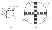
図1は、本発明に係る電力変換装置の実施の形態1を説明するための平面図である。図2(a)は、半導体モジュールの平面図、図2(b)は図2(a)の半導体モジュールに対応する回路図である。
FIG. 1 is a plan view for explaining a first embodiment of a power conversion device according to the present invention. FIG. 2A is a plan view of the semiconductor module, and FIG. 2B is a circuit diagram corresponding to the semiconductor module of FIG.
図2に示したように、半導体モジュール1aは、AC出力端子(以下、AC端子と称す)2a、陽極直流入力端子(以下、P端子と称す)2b、陰極入力端子(以下、N端子と称す)2c、上アーム側IGBT3a、下アーム側IGBT3b、上アーム側FWD4a、下アーム側FWD4b、ヒートスプレッダ6を備え、IGBT3aとFWD4aとAC端子2a及びIGBT3bとFWD4bとN端子2cはそれぞれワイヤボンド5で電気的に接続されて、モールド樹脂8によりモールドされている。図2(b)の回路は典型的な電力変換装置の1相分に相当するスイッチング素子である。電力変換装置には3相分のスイッチング素子が搭載され、P端子2b、N端子2cにそれぞれバッテリの正極、負極が接続され、各相のAC端子2aは負荷(ハイブリッド自動車の場合はモーター)に接続される。そして、各スイッチング素子を高速で開閉し、そのタイミングを制御することで、負荷に所望の交流電力を供給する。
As shown in FIG. 2, the
図1は、図2で説明した半導体モジュールを2個並列接続した図である。半導体モジュール1aと半導体モジュール1bは2つで1相分の回路を形成しており、図に示すように鏡面対称面7に対して主端子の組(P端子2b、N端子2c及びAC端子2a)の同極の主端子同士が鏡面対象の関係になっている。このような構造にすることで、主端子の組(P端子2b、N端子2c及びAC端子2a)の同極の主端子同士が直接接して接続されるので、主端子間をつなぐバスバーを設ける必要がなくなり、半導体モジュール1a,1bを並列接続して大容量化した電力変換装置をコンパクトにすることができる。
FIG. 1 is a diagram in which two semiconductor modules described in FIG. 2 are connected in parallel. Two
また、さらに、鏡面対称面7に対してパワー部の配線が鏡面対象の関係になっているので、配線を短くすることができる。 Furthermore, since the wiring of the power part is in a mirror surface relationship with respect to the mirror plane 7, the wiring can be shortened.
実施の形態2.
図3乃至図5は、本発明に係る電力変換装置の実施の形態2を説明する平面図である。図3(a)に示したように、一つの半導体モジュール1から主端子の組(P端子2b、N端子2c及びAC端子2a)が2組設けられており、それらが図2(b)に示すように同極の主端子同士が鏡面対象となるように配置され、直接接して接続される。これによりバスバーを用いずに複数の半導体モジュールを並列接続することとができ、大容量化した電力変換装置をコンパクトにすることができる。
Embodiment 2. FIG.
3 to 5 are plan views for explaining Embodiment 2 of the power conversion device according to the present invention. As shown in FIG. 3 (a), two sets of main terminals (
本実施の形態2においては、図3及び図4に示したように、矩形または正方形、扇形などの半導体モジュール1に主端子の組が2組設けられ、同極の主端子同士が鏡面対象となるように配置され、直接接して接続されるような変形例も考えられる。
In the second embodiment, as shown in FIG. 3 and FIG. 4, two sets of main terminals are provided in the
本実施の形態2の説明では主端子の組が2組の場合を取り上げて説明したが、主端子の組の数はこれに制限されるものではない。また、主端子の組の数によって種々の半導体モジュールの形や配置が可能である。 In the description of the second embodiment, the case where there are two sets of main terminals has been described. However, the number of sets of main terminals is not limited to this. Various shapes and arrangements of semiconductor modules are possible depending on the number of sets of main terminals.
実施の形態3.
図6は、本発明に係る電力変換装置の実施の形態3を説明する側面図(a)及び正面図(b)である。図6(a)に示したように、半導体モジュール1から突き出した主端子2を、半導体モジュール近傍で直角に曲げ、半導体モジュール上方で、図6(b)に示すような多点で溶接をはじめとする金属接合9により接続する。
Embodiment 3 FIG.
FIG. 6: is the side view (a) and front view (b) explaining Embodiment 3 of the power converter device which concerns on this invention. As shown in FIG. 6A, the main terminal 2 protruding from the
上記実施の形態1及び2において、通常、主端子間の接続は機械締結が用いられることが一般的であるが、本実施の形態3のように、金属接合9による接合とすることで、機械締結の場合に比べ、ネジのスペース等が省略されるため、電力変換装置の容積をさらに小さくできる。
In the first and second embodiments, the connection between the main terminals is usually performed by mechanical fastening. However, as in the third embodiment, the connection by the
なお、図6に、半導体モジュール1から突き出した主端子2を、半導体モジュール近傍で直角に曲げた形状の例を示したが、本発明の主端子の形状は、図6の主端子の形状に制限されるものではない。
6 shows an example of a shape in which the main terminal 2 protruding from the
本発明に係る電力変換装置は、比較的容量の大きい電力変換装置、特にハイブリッド自動車や電気自動車で使用される電力変換装置に有効に利用できる。 The power converter according to the present invention can be effectively used for a power converter having a relatively large capacity, particularly a power converter used in a hybrid vehicle or an electric vehicle.
1,1a,1b 半導体モジュール、2a AC端子(主端子)、
2b P端子(主端子)、2c N端子(主端子)、3a 上アーム側IGBT、
3b 下アーム側IGBT、4a 上アーム側FWD、4b 下アーム側FWD、
5 ワイヤーボンド、7 鏡面対称面、8 モールド樹脂、9 溶接部。
1, 1a, 1b semiconductor module, 2a AC terminal (main terminal),
2b P terminal (main terminal), 2c N terminal (main terminal), 3a Upper arm side IGBT,
3b Lower arm side IGBT, 4a Upper arm side FWD, 4b Lower arm side FWD,
5 Wire bond, 7 Mirror plane, 8 Mold resin, 9 Welded part.
Claims (3)
上記半導体モジュールはそれぞれ、スイッチング素子と該スイッチング素子が配線により接続された複数の主端子とを有し、
上記半導体モジュール相互の同一極性の主端子同士を直接接触させて接続したことを特徴とする電力変換装置。 In the power conversion device in which each phase in the power conversion circuit is formed by electrically connecting a plurality of semiconductor modules in parallel,
Each of the semiconductor modules has a switching element and a plurality of main terminals to which the switching element is connected by wiring,
A power conversion device, wherein the main terminals of the same polarity of the semiconductor modules are connected in direct contact with each other.
Priority Applications (1)
| Application Number | Priority Date | Filing Date | Title |
|---|---|---|---|
| JP2005301502A JP4567570B2 (en) | 2005-10-17 | 2005-10-17 | Power converter |
Applications Claiming Priority (1)
| Application Number | Priority Date | Filing Date | Title |
|---|---|---|---|
| JP2005301502A JP4567570B2 (en) | 2005-10-17 | 2005-10-17 | Power converter |
Publications (3)
| Publication Number | Publication Date |
|---|---|
| JP2007110870A JP2007110870A (en) | 2007-04-26 |
| JP2007110870A5 JP2007110870A5 (en) | 2007-11-29 |
| JP4567570B2 true JP4567570B2 (en) | 2010-10-20 |
Family
ID=38036272
Family Applications (1)
| Application Number | Title | Priority Date | Filing Date |
|---|---|---|---|
| JP2005301502A Active JP4567570B2 (en) | 2005-10-17 | 2005-10-17 | Power converter |
Country Status (1)
| Country | Link |
|---|---|
| JP (1) | JP4567570B2 (en) |
Families Citing this family (13)
| Publication number | Priority date | Publication date | Assignee | Title |
|---|---|---|---|---|
| JP4667476B2 (en) * | 2008-02-18 | 2011-04-13 | 三菱電機株式会社 | Electrical component connection method and connection structure, and power conversion device using the connection structure |
| JP5532955B2 (en) * | 2010-01-22 | 2014-06-25 | 株式会社デンソー | Rotating electric machine for vehicles |
| JP5213884B2 (en) | 2010-01-27 | 2013-06-19 | 三菱電機株式会社 | Semiconductor device module |
| JP5532984B2 (en) * | 2010-02-04 | 2014-06-25 | 株式会社デンソー | Rotating electric machine for vehicles |
| JP5464159B2 (en) * | 2011-03-08 | 2014-04-09 | 三菱電機株式会社 | Power module |
| DE112013001234B4 (en) * | 2012-03-01 | 2023-02-02 | Mitsubishi Electric Corporation | Power semiconductor module and energy conversion device |
| JP2014033118A (en) * | 2012-08-06 | 2014-02-20 | Mitsubishi Electric Corp | Semiconductor module pair and semiconductor device |
| WO2015121899A1 (en) * | 2014-02-11 | 2015-08-20 | 三菱電機株式会社 | Power semiconductor module |
| JP6223296B2 (en) * | 2014-07-29 | 2017-11-01 | 三菱電機株式会社 | Semiconductor device |
| JP2017050488A (en) | 2015-09-04 | 2017-03-09 | 株式会社東芝 | Semiconductor package |
| EP3246945B1 (en) * | 2016-05-19 | 2018-10-03 | ABB Schweiz AG | Power module with low stray inductance |
| JP6702154B2 (en) | 2016-11-21 | 2020-05-27 | 株式会社デンソー | Switch drive |
| JP7099422B2 (en) * | 2019-09-10 | 2022-07-12 | 株式会社デンソー | Power converter |
Citations (5)
| Publication number | Priority date | Publication date | Assignee | Title |
|---|---|---|---|---|
| JPH08316382A (en) * | 1994-05-02 | 1996-11-29 | Motorola Inc | Electronic module for removing heat from semiconductor die and its preparation |
| JP2000308364A (en) * | 1999-04-22 | 2000-11-02 | Fuji Electric Co Ltd | Semiconductor power conversion circuit |
| JP2003018863A (en) * | 2001-07-03 | 2003-01-17 | Mitsubishi Electric Corp | Power semiconductor device |
| JP2004022968A (en) * | 2002-06-19 | 2004-01-22 | Mitsubishi Electric Corp | Semiconductor device and method of manufacturing the same |
| JP2005198443A (en) * | 2004-01-08 | 2005-07-21 | Toyota Industries Corp | Semiconductor device and manufacturing method therefor |
-
2005
- 2005-10-17 JP JP2005301502A patent/JP4567570B2/en active Active
Patent Citations (5)
| Publication number | Priority date | Publication date | Assignee | Title |
|---|---|---|---|---|
| JPH08316382A (en) * | 1994-05-02 | 1996-11-29 | Motorola Inc | Electronic module for removing heat from semiconductor die and its preparation |
| JP2000308364A (en) * | 1999-04-22 | 2000-11-02 | Fuji Electric Co Ltd | Semiconductor power conversion circuit |
| JP2003018863A (en) * | 2001-07-03 | 2003-01-17 | Mitsubishi Electric Corp | Power semiconductor device |
| JP2004022968A (en) * | 2002-06-19 | 2004-01-22 | Mitsubishi Electric Corp | Semiconductor device and method of manufacturing the same |
| JP2005198443A (en) * | 2004-01-08 | 2005-07-21 | Toyota Industries Corp | Semiconductor device and manufacturing method therefor |
Also Published As
| Publication number | Publication date |
|---|---|
| JP2007110870A (en) | 2007-04-26 |
Similar Documents
| Publication | Publication Date | Title |
|---|---|---|
| JP4567570B2 (en) | Power converter | |
| US9390996B2 (en) | Double-sided cooling power module and method for manufacturing the same | |
| CN101330248B (en) | Power converter device | |
| JP4988665B2 (en) | Semiconductor device and power conversion device using the semiconductor device | |
| US8519561B2 (en) | Power module and vehicle-mounted inverter using the same | |
| WO2012073306A1 (en) | Power module | |
| JP2003009546A (en) | Power converter and mobile body provided therewith | |
| CN103597729A (en) | Power module and power conversion apparatus using same | |
| JP2008086099A (en) | Inverter device | |
| CN108112217B (en) | Inverter structure for vehicle | |
| JP6312228B2 (en) | Power converter | |
| US11424689B2 (en) | Power conversion device | |
| US20230328938A1 (en) | Power module | |
| US10615156B2 (en) | Power module | |
| JP5202366B2 (en) | Semiconductor device | |
| JP5202365B2 (en) | Semiconductor device | |
| JP7294058B2 (en) | power converter | |
| JP2013223384A (en) | Power conversion apparatus and vehicle | |
| JP5919424B1 (en) | Capacitor module | |
| JP6447914B2 (en) | DC module wiring board for power module and manufacturing method thereof | |
| JP2014212193A (en) | Stack type cooling device for semiconductor module | |
| JP2020145320A (en) | Semiconductor device | |
| JP7180455B2 (en) | power conversion unit | |
| CN218829508U (en) | Novel motor controller, drive assembly and vehicle of arranging | |
| WO2023058381A1 (en) | Power conversion device |
Legal Events
| Date | Code | Title | Description |
|---|---|---|---|
| A521 | Request for written amendment filed |
Free format text: JAPANESE INTERMEDIATE CODE: A523 Effective date: 20071015 |
|
| A621 | Written request for application examination |
Free format text: JAPANESE INTERMEDIATE CODE: A621 Effective date: 20071015 |
|
| TRDD | Decision of grant or rejection written | ||
| A01 | Written decision to grant a patent or to grant a registration (utility model) |
Free format text: JAPANESE INTERMEDIATE CODE: A01 Effective date: 20100803 |
|
| A977 | Report on retrieval |
Free format text: JAPANESE INTERMEDIATE CODE: A971007 Effective date: 20100805 |
|
| A01 | Written decision to grant a patent or to grant a registration (utility model) |
Free format text: JAPANESE INTERMEDIATE CODE: A01 |
|
| A61 | First payment of annual fees (during grant procedure) |
Free format text: JAPANESE INTERMEDIATE CODE: A61 Effective date: 20100805 |
|
| R150 | Certificate of patent or registration of utility model |
Ref document number: 4567570 Country of ref document: JP Free format text: JAPANESE INTERMEDIATE CODE: R150 Free format text: JAPANESE INTERMEDIATE CODE: R150 |
|
| FPAY | Renewal fee payment (event date is renewal date of database) |
Free format text: PAYMENT UNTIL: 20130813 Year of fee payment: 3 |
|
| R250 | Receipt of annual fees |
Free format text: JAPANESE INTERMEDIATE CODE: R250 |
|
| R250 | Receipt of annual fees |
Free format text: JAPANESE INTERMEDIATE CODE: R250 |
|
| R250 | Receipt of annual fees |
Free format text: JAPANESE INTERMEDIATE CODE: R250 |
|
| R250 | Receipt of annual fees |
Free format text: JAPANESE INTERMEDIATE CODE: R250 |
|
| R250 | Receipt of annual fees |
Free format text: JAPANESE INTERMEDIATE CODE: R250 |
|
| R250 | Receipt of annual fees |
Free format text: JAPANESE INTERMEDIATE CODE: R250 |
|
| R250 | Receipt of annual fees |
Free format text: JAPANESE INTERMEDIATE CODE: R250 |
|
| R250 | Receipt of annual fees |
Free format text: JAPANESE INTERMEDIATE CODE: R250 |
|
| R250 | Receipt of annual fees |
Free format text: JAPANESE INTERMEDIATE CODE: R250 |
|
| R250 | Receipt of annual fees |
Free format text: JAPANESE INTERMEDIATE CODE: R250 |