WO2023058381A1 - Power conversion device - Google Patents
Power conversion device Download PDFInfo
- Publication number
- WO2023058381A1 WO2023058381A1 PCT/JP2022/033303 JP2022033303W WO2023058381A1 WO 2023058381 A1 WO2023058381 A1 WO 2023058381A1 JP 2022033303 W JP2022033303 W JP 2022033303W WO 2023058381 A1 WO2023058381 A1 WO 2023058381A1
- Authority
- WO
- WIPO (PCT)
- Prior art keywords
- bus bar
- module
- semiconductor
- lower arm
- upper arm
- Prior art date
Links
- 238000006243 chemical reaction Methods 0.000 title claims description 44
- 239000004065 semiconductor Substances 0.000 claims abstract description 143
- 239000003990 capacitor Substances 0.000 claims abstract description 87
- 238000003475 lamination Methods 0.000 claims abstract description 6
- 238000007789 sealing Methods 0.000 claims description 20
- 229910052751 metal Inorganic materials 0.000 description 57
- 239000002184 metal Substances 0.000 description 57
- 239000000758 substrate Substances 0.000 description 30
- 239000000463 material Substances 0.000 description 18
- 230000006870 function Effects 0.000 description 12
- 238000009499 grossing Methods 0.000 description 10
- 239000003507 refrigerant Substances 0.000 description 8
- 230000004048 modification Effects 0.000 description 7
- 238000012986 modification Methods 0.000 description 7
- 229920005989 resin Polymers 0.000 description 6
- 239000011347 resin Substances 0.000 description 6
- 230000000694 effects Effects 0.000 description 4
- 230000017525 heat dissipation Effects 0.000 description 4
- 238000005304 joining Methods 0.000 description 4
- LYCAIKOWRPUZTN-UHFFFAOYSA-N Ethylene glycol Chemical compound OCCO LYCAIKOWRPUZTN-UHFFFAOYSA-N 0.000 description 3
- 229910052782 aluminium Inorganic materials 0.000 description 3
- 238000010586 diagram Methods 0.000 description 3
- 230000004907 flux Effects 0.000 description 3
- 238000004904 shortening Methods 0.000 description 3
- 238000003466 welding Methods 0.000 description 3
- 238000004804 winding Methods 0.000 description 3
- QGZKDVFQNNGYKY-UHFFFAOYSA-N Ammonia Chemical compound N QGZKDVFQNNGYKY-UHFFFAOYSA-N 0.000 description 2
- 241000156302 Porcine hemagglutinating encephalomyelitis virus Species 0.000 description 2
- XUIMIQQOPSSXEZ-UHFFFAOYSA-N Silicon Chemical compound [Si] XUIMIQQOPSSXEZ-UHFFFAOYSA-N 0.000 description 2
- XAGFODPZIPBFFR-UHFFFAOYSA-N aluminium Chemical compound [Al] XAGFODPZIPBFFR-UHFFFAOYSA-N 0.000 description 2
- 239000000919 ceramic Substances 0.000 description 2
- 239000008393 encapsulating agent Substances 0.000 description 2
- 239000007769 metal material Substances 0.000 description 2
- 230000002093 peripheral effect Effects 0.000 description 2
- 238000012545 processing Methods 0.000 description 2
- 229910052710 silicon Inorganic materials 0.000 description 2
- 239000010703 silicon Substances 0.000 description 2
- 241001184547 Agrostis capillaris Species 0.000 description 1
- JMASRVWKEDWRBT-UHFFFAOYSA-N Gallium nitride Chemical compound [Ga]#N JMASRVWKEDWRBT-UHFFFAOYSA-N 0.000 description 1
- HBBGRARXTFLTSG-UHFFFAOYSA-N Lithium ion Chemical compound [Li+] HBBGRARXTFLTSG-UHFFFAOYSA-N 0.000 description 1
- 229910021529 ammonia Inorganic materials 0.000 description 1
- 230000002457 bidirectional effect Effects 0.000 description 1
- 238000005219 brazing Methods 0.000 description 1
- 239000011248 coating agent Substances 0.000 description 1
- 238000000576 coating method Methods 0.000 description 1
- 238000010276 construction Methods 0.000 description 1
- 239000002826 coolant Substances 0.000 description 1
- 229910052802 copper Inorganic materials 0.000 description 1
- 229910003460 diamond Inorganic materials 0.000 description 1
- 239000010432 diamond Substances 0.000 description 1
- AJNVQOSZGJRYEI-UHFFFAOYSA-N digallium;oxygen(2-) Chemical compound [O-2].[O-2].[O-2].[Ga+3].[Ga+3] AJNVQOSZGJRYEI-UHFFFAOYSA-N 0.000 description 1
- 230000005489 elastic deformation Effects 0.000 description 1
- 239000003822 epoxy resin Substances 0.000 description 1
- 230000005669 field effect Effects 0.000 description 1
- 239000000945 filler Substances 0.000 description 1
- 239000011888 foil Substances 0.000 description 1
- 238000003780 insertion Methods 0.000 description 1
- 230000037431 insertion Effects 0.000 description 1
- 229910001416 lithium ion Inorganic materials 0.000 description 1
- 229910052987 metal hydride Inorganic materials 0.000 description 1
- 229910044991 metal oxide Inorganic materials 0.000 description 1
- 150000004706 metal oxides Chemical class 0.000 description 1
- 238000005272 metallurgy Methods 0.000 description 1
- 238000000034 method Methods 0.000 description 1
- 238000000465 moulding Methods 0.000 description 1
- 229910052759 nickel Inorganic materials 0.000 description 1
- PXHVJJICTQNCMI-UHFFFAOYSA-N nickel Substances [Ni] PXHVJJICTQNCMI-UHFFFAOYSA-N 0.000 description 1
- -1 nickel metal hydride Chemical class 0.000 description 1
- 230000003071 parasitic effect Effects 0.000 description 1
- 229920000647 polyepoxide Polymers 0.000 description 1
- 238000004382 potting Methods 0.000 description 1
- 238000003825 pressing Methods 0.000 description 1
- 230000009467 reduction Effects 0.000 description 1
- 230000001172 regenerating effect Effects 0.000 description 1
- 230000008929 regeneration Effects 0.000 description 1
- 238000011069 regeneration method Methods 0.000 description 1
- 239000003566 sealing material Substances 0.000 description 1
- HBMJWWWQQXIZIP-UHFFFAOYSA-N silicon carbide Chemical compound [Si+]#[C-] HBMJWWWQQXIZIP-UHFFFAOYSA-N 0.000 description 1
- 238000005549 size reduction Methods 0.000 description 1
- 229910000679 solder Inorganic materials 0.000 description 1
- 238000005476 soldering Methods 0.000 description 1
- 239000007787 solid Substances 0.000 description 1
- 125000006850 spacer group Chemical group 0.000 description 1
- 238000001721 transfer moulding Methods 0.000 description 1
- XLYOFNOQVPJJNP-UHFFFAOYSA-N water Substances O XLYOFNOQVPJJNP-UHFFFAOYSA-N 0.000 description 1
Images


Classifications
-
- H—ELECTRICITY
- H02—GENERATION; CONVERSION OR DISTRIBUTION OF ELECTRIC POWER
- H02M—APPARATUS FOR CONVERSION BETWEEN AC AND AC, BETWEEN AC AND DC, OR BETWEEN DC AND DC, AND FOR USE WITH MAINS OR SIMILAR POWER SUPPLY SYSTEMS; CONVERSION OF DC OR AC INPUT POWER INTO SURGE OUTPUT POWER; CONTROL OR REGULATION THEREOF
- H02M7/00—Conversion of ac power input into dc power output; Conversion of dc power input into ac power output
- H02M7/42—Conversion of dc power input into ac power output without possibility of reversal
- H02M7/44—Conversion of dc power input into ac power output without possibility of reversal by static converters
- H02M7/48—Conversion of dc power input into ac power output without possibility of reversal by static converters using discharge tubes with control electrode or semiconductor devices with control electrode
Definitions
- the disclosure in this specification relates to a power converter.
- Patent Document 1 discloses a power converter.
- This power converter includes a plurality of semiconductor modules, a cooler, a condenser, and a plurality of busbars.
- the cooler has a plurality of heat exchanging portions arranged in multiple stages so as to sandwich each of the semiconductor modules from both sides.
- the plurality of busbars includes power busbars electrically connecting the capacitors and the semiconductor modules.
- each semiconductor module constitutes an upper and lower arm circuit for one phase.
- Such a semiconductor module has therein a semiconductor element forming an upper arm and a semiconductor element forming a lower arm, and these semiconductor elements are arranged side by side in one direction orthogonal to the stacking direction.
- the PN current loop becomes large within the semiconductor module.
- the capacitor is arranged in one direction orthogonal to the stacking direction with respect to the stack of the semiconductor module and the heat exchange portion.
- a pipe is arranged between the semiconductor module and the condenser to introduce or discharge the refrigerant to or from the heat exchange section. Therefore, the power bus bar must be routed across the pipes of the cooler, resulting in a long power bus bar. Further improvements are required for the power conversion device from the above viewpoints or from other viewpoints not mentioned.
- One object of the disclosure is to provide a power conversion device capable of reducing inductance.
- the power conversion device disclosed here is a plurality of semiconductor modules including an upper arm module forming an upper arm of the upper and lower arm circuits, and a lower arm module forming a lower arm of the upper and lower arm circuits and arranged side by side with the upper arm modules in the stacking direction; a cooler having a plurality of heat exchange portions arranged in multiple stages so as to cool the upper arm module and the lower arm module from both sides in the stacking direction and forming a laminate together with the plurality of semiconductor modules; a capacitor arranged on one end side of the laminate in the lamination direction; a plurality of bus bars including a power supply bus bar that electrically connects the capacitor and the semiconductor module and extends in the stacking direction so as to straddle at least one of the heat exchanging parts.
- a plurality of semiconductor modules are divided into upper arm modules and lower arm modules, and the upper arm modules and lower arm modules are arranged side by side in the stacking direction.
- the capacitors are arranged in the stacking direction with respect to the stack, and the power supply bus bar is extended in the stacking direction so as to straddle at least one of the heat exchange portions.
- the length of the power busbar that is, the current path can be shortened.
- FIG. 1 is a perspective view showing a semiconductor module
- FIG. 2 is a plan view showing the arrangement of a semiconductor element, surface metal bodies of a substrate, and main terminals; It is a top view which shows a laminated body.
- FIG. 2 is a plan view showing the arrangement of semiconductor modules, coolers, and capacitors;
- FIG. 10 is a cross-sectional view taken along line XX of FIG.
- FIG. 4 is a plan view showing the arrangement of a laminate and busbars
- FIG. 10 is a perspective view showing a state before connecting the extended portion of the negative bus bar
- FIG. 10 is a perspective view showing a state after connecting the extended portion of the negative bus bar
- FIG. 11 shows a PN current loop
- FIG. 4 is a diagram showing current paths
- FIG. 4 is a diagram showing current paths
- It is a figure which shows the circuit structure of the power converter device which concerns on 2nd Embodiment.
- 1 is a perspective view showing a semiconductor module
- FIG. FIG. 11 is a plan view showing the arrangement of a laminate and busbars in a power conversion device according to a third embodiment
- FIG. 10 is a perspective view showing a state before connecting the extended portion of the negative bus bar
- FIG. 10 is a perspective view showing a state after connecting the extended portion of the negative bus bar;
- the power conversion device of this embodiment is applied, for example, to a moving body that uses a rotating electric machine as a drive source.
- Mobile objects include, for example, electric vehicles such as electric vehicles (BEV), hybrid vehicles (HEV), and plug-in hybrid vehicles (PHEV), flying vehicles such as drones, ships, construction machinery, and agricultural machinery.
- BEV electric vehicles
- HEV hybrid vehicles
- PHEV plug-in hybrid vehicles
- flying vehicles such as drones, ships, construction machinery, and agricultural machinery.
- a vehicle drive system 1 includes a DC power supply 2 , a motor generator 3 , and a power conversion device 4 .
- the DC power supply 2 is a DC voltage source composed of a rechargeable secondary battery. Secondary batteries are, for example, lithium ion batteries and nickel metal hydride batteries.
- the motor generator 3 is a three-phase alternating-current rotating electric machine. The motor generator 3 functions as a vehicle drive source, that is, as an electric motor. The motor generator 3 functions as a generator during regeneration.
- the power converter 4 performs power conversion between the DC power supply 2 and the motor generator 3 .
- FIG. 1 shows the circuit configuration of the power conversion device 4.
- the power conversion device 4 includes a power conversion circuit.
- the power conversion device 4 of this embodiment includes a smoothing capacitor 5 , an inverter 6 that is a power conversion circuit, and a drive circuit 7 .
- the smoothing capacitor 5 mainly smoothes the DC voltage supplied from the DC power supply 2 .
- the smoothing capacitor 5 is connected to a P line 8 that is a power supply line on the high potential side and an N line 9 that is a power supply line on the low potential side.
- the P line 8 is connected to the positive pole of the DC power supply 2 and the N line 9 is connected to the negative pole of the DC power supply 2 .
- the positive terminal of smoothing capacitor 5 is connected to P line 8 between DC power supply 2 and inverter 6 .
- the negative electrode of smoothing capacitor 5 is connected to N line 9 between DC power supply 2 and inverter 6 .
- a smoothing capacitor 5 is connected in parallel with the DC power supply 2 .
- the inverter 6 is a DC-AC conversion circuit. Inverter 6 converts the DC voltage into a three-phase AC voltage and outputs it to motor generator 3 according to switching control by a control circuit (not shown). Thereby, the motor generator 3 is driven to generate a predetermined torque. During regenerative braking of the vehicle, inverter 6 converts the three-phase AC voltage generated by motor generator 3 by receiving torque from the wheels into DC voltage according to switching control by the control circuit, and outputs the DC voltage to P line 8 . Thus, inverter 6 performs bidirectional power conversion between DC power supply 2 and motor generator 3 .
- the inverter 6 is configured with upper and lower arm circuits 10 for three phases.
- the upper and lower arm circuits 10 are sometimes called legs.
- the upper and lower arm circuits 10 each have an upper arm 10H and a lower arm 10L.
- the upper arm 10H and the lower arm 10L may be simply referred to as arms 10H and 10L.
- the upper arm 10H and the lower arm 10L are connected in series between the P line 8 and the N line 9 with the upper arm 10H on the P line 8 side.
- a connection point between the upper arm 10H and the lower arm 10L is connected to a corresponding phase winding 3a in the motor generator 3 via an output line 11.
- the inverter 6 has six arms 10H and 10L. Each arm 10H, 10L is configured with a switching element.
- an n-channel insulated gate bipolar transistor 12 (hereinafter referred to as IGBT 12) is employed as a switching element forming each arm 10H, 10L.
- IGBT is an abbreviation for Insulated Gate Bipolar Transistor.
- a freewheeling diode 13 (hereinafter referred to as FWD 13) is connected in anti-parallel to each of the IGBTs 12 .
- the collector of the IGBT 12 is connected to the P line 8 in the upper arm 10H.
- the emitter of IGBT 12 is connected to N line 9 in lower arm 10L.
- the emitter of IGBT 12 in upper arm 10H and the collector of IGBT 12 in lower arm 10L are connected to each other.
- the anode of FWD 13 is connected to the corresponding emitter of IGBT 12, and the cathode is connected to the collector.
- the switching element is not limited to the IGBT 12.
- a MOSFET may be employed.
- MOSFET is an abbreviation for Metal Oxide Semiconductor Field Effect Transistor.
- a parasitic diode (body diode) may be used as a freewheeling diode, or an external diode may be used.
- the drive circuit 7 drives switching elements that make up a power conversion circuit such as the inverter 6 .
- the drive circuit 7 supplies a drive voltage to the gates of the IGBTs 12 of the corresponding arms 10H and 10L based on drive commands from the control circuit.
- the drive circuit drives the corresponding IGBT 12 by applying a drive voltage, that is, ON drive and OFF drive.
- a driving circuit is sometimes referred to as a driver.
- the power conversion device 4 may include a control circuit for switching elements.
- the control circuit generates a drive command for operating the IGBT 12 and outputs it to the drive circuit 7 .
- the control circuit generates a drive command based on, for example, a torque request input from a host ECU (not shown) and signals detected by various sensors.
- ECU is an abbreviation for Electronic Control Unit.
- the control circuit may be provided in the host ECU.
- Various sensors include, for example, current sensors, rotation angle sensors, and voltage sensors.
- Power conversion device 4 may include at least one of the sensors.
- the current sensor detects a phase current flowing through each phase winding 3a.
- the rotation angle sensor detects the rotation angle of the rotor of motor generator 3 .
- a voltage sensor detects the voltage across the smoothing capacitor 5 .
- the control circuit comprises, for example, a processor and memory.
- the control circuit outputs, for example, a PWM signal as the drive command.
- PWM is an abbreviation for Pulse Width Modulation.
- the power conversion device 4 may include a converter as a power conversion circuit.
- a converter is a DC-DC conversion circuit that converts a DC voltage into DC voltages of different values.
- the converter is provided between the DC power supply 2 and the smoothing capacitor 5 .
- the converter includes, for example, a reactor and the upper and lower arm circuits 10 described above. According to this configuration, it is possible to step up and down.
- the power conversion device 4 may include a filter capacitor that removes power noise from the DC power supply 2 .
- a filter capacitor is provided between the DC power supply 2 and the converter.
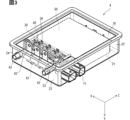
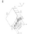
- FIG. 2 shows the power conversion device 4 .
- FIG. 3 is an inverted view with respect to FIG.
- FIG. 4 is an exploded perspective view.
- FIG. 5 shows the structure inside the case 20 .
- FIG. 5 omits the case 20 with respect to FIG. In FIGS. 2 to 5, the inside is shown transparently.
- the power converter 4 includes a case 20, a plurality of semiconductor modules 30, a cooler 40, a capacitor module 50, a busbar 60, a circuit board 70, and the like.
- the stacking direction of the semiconductor module 30 and the heat exchange section 41 of the cooler 40 is defined as the Z direction.
- the direction perpendicular to the Z direction and in which the semiconductor modules 30 on the same arm are arranged is defined as the X direction.
- a direction perpendicular to both the Z direction and the X direction is defined as the Y direction.
- the X direction, Y direction, and Z direction are in a positional relationship orthogonal to each other.
- Case 20 accommodates other elements that configure power converter 4 .
- the case 20 is, for example, an aluminum die-cast molding. As shown in FIGS. 2 to 4, the case 20 of this embodiment has a box shape with one side open. One surface of the case 20 is open in the Y direction.
- the case 20 has a bottom wall 21 and side walls 22 .
- the bottom wall 21 has a substantially rectangular planar shape.
- the side wall 22 continues to the bottom wall 21 and extends from the bottom wall 21 in the Y direction.
- the side wall 22 continues to each of the four sides of the outer peripheral edge of the bottom wall 21 .
- the side wall 22 has a substantially rectangular annular shape when viewed from above in the Y direction. Case 20 has four side walls 22 .
- the case 20 has through holes 23 and 24 in one of the side walls 22 . Pipes 42 and 43 of the cooler 40 are inserted through the through holes 23 and 24 .
- the through-holes 23 and 24 pass through the side wall 22 from inside to outside, and are open to the inside and the outside.
- the case 20 has openings (not shown) for electrically connecting the connectors 71 and 80 to the outside of the power converter 4 .
- Case 20 has an opening for connector 71 and an opening for connector 80 .
- the opening is, for example, a through hole or a notch provided in side wall 22 .
- the power conversion device 4 may include a cover (lid) that closes the opening on one side of the case 20 together with the case 20 .
- the case 20 and cover are sometimes referred to as a housing.
- a filler such as potting resin may be placed in the case 20 to liquid-tightly seal the elements housed in the case 20 .
- sealing materials are applied to the portions facing the case 20 and the cover, the portions facing the walls of the through holes 23 and 24 and the pipes 42 and 43, and the portions facing the housings of the connectors 71 and 80 and the walls of the openings. , the inside of the housing may be liquid-tightly sealed.
- FIG. 6 shows a semiconductor module 30. As shown in FIG. FIG. 6 shows the upper arm module 30H as an example.
- FIG. 7 shows the arrangement of the semiconductor element 32 , the surface metal bodies 332 and 342 of the substrates 33 and 34 , and the main terminals 35 in the semiconductor module 30 .
- the substrate 34 is shown reversed 180 with respect to the substrate 33, and the surface metal bodies 332, 342 of the substrates 33, 34 are shown on the same plane for easy understanding of the arrangement.
- a plurality of semiconductor modules 30 constitute the upper and lower arm circuits 10 described above, that is, the inverter 6 (power conversion circuit).
- the multiple semiconductor modules 30 include an upper arm module 30H forming the upper arm 10H and a lower arm module 30L forming the lower arm 10L.
- one semiconductor module 30 constitutes one arm 10H, 10L.
- the plurality of semiconductor modules 30 includes three upper arm modules 30H forming upper arms 10H for three phases and three lower arm modules 30L forming lower arms 10L for three phases. contains. Also, all semiconductor modules 30 have a common structure. As shown in FIGS. 6 and 7, each semiconductor module 30 includes a sealing body 31, a semiconductor element 32, substrates 33 and 34, main terminals 35, and signal terminals .
- the encapsulant 31 encapsulates part of other elements that constitute the semiconductor module 30 .
- the rest of the other elements are exposed outside the encapsulant 31 .
- Sealing body 31 is made of resin, for example.
- the sealing body 31 is formed by a transfer molding method using, for example, an epoxy resin as a material.
- Sealing body 31 may be formed using gel, for example. The gel is filled (arranged) in opposing regions of the pair of substrates 33 and 34, for example.
- the semiconductor element 32 is formed by forming a switching element on a semiconductor substrate made of silicon (Si), a wide bandgap semiconductor having a wider bandgap than silicon, or the like.
- the switching element has a vertical structure so that the main current flows in the thickness direction of the semiconductor substrate.
- Wide bandgap semiconductors include, for example, silicon carbide (SiC), gallium nitride (GaN), gallium oxide (Ga2O3), and diamond.
- the semiconductor element 32 may be called a power element, a semiconductor chip, or the like.
- the semiconductor element 32 of the present embodiment is formed by forming the above-described n-channel type IGBT 12 and FWD 13, ie RC (Reverse Conducting)-IGBT, on a semiconductor substrate made of Si.
- the IGBT 12 has a vertical structure so that the main current flows in the thickness direction of the semiconductor element 32 (semiconductor substrate).
- the semiconductor element 32 has main electrodes of switching elements on both sides thereof in the plate thickness direction. Specifically, as main electrodes, it has an emitter electrode 32E on the front surface and a collector electrode 32C on the back surface. An emitter electrode 32E is formed on a portion of the surface.
- the collector electrode 32C is formed over substantially the entire back surface. In FIG. 7, the collector electrode 32C and the emitter electrode 32E are indicated by dashed lines.
- the semiconductor element 32 has a pad (not shown) as a signal electrode on the surface on which the emitter electrode 32E is formed.
- the semiconductor element 32 is arranged such that its plate thickness direction is substantially parallel to the Z direction.
- the semiconductor module 30 of this embodiment includes one semiconductor element 32 .
- the substrates 33 and 34 are arranged so as to sandwich the semiconductor element 32 in the plate thickness direction of the semiconductor element 32, that is, in the Z direction.
- the substrates 33 and 34 are arranged so that at least parts of them face each other in the Z direction.
- the substrates 33 and 34 contain all of the semiconductor elements 32 that form the arms 10H and 10L when viewed from above in the Z direction.
- the substrates 33 , 34 are electrically connected to the semiconductor element 32 .
- the substrate 33 is arranged on the collector electrode 32C side with respect to the semiconductor element 32 .
- the substrate 34 is arranged on the emitter electrode 32E side with respect to the semiconductor element 32 .
- the substrate 33 is electrically connected to the collector electrode 32C and provides a wiring function.
- substrate 34 is electrically connected to emitter electrode 32E and provides a wiring function.
- the substrates 33 and 34 provide a heat dissipation function for dissipating heat generated by the semiconductor element 32 .
- the substrate 33 has an insulating base material 331 , a front metal body 332 and a back metal body 333 .
- the surface metal body 332 is arranged on the surface of the insulating base material 331 on the side of the semiconductor element 32 .
- the back metal body 333 is arranged on the back surface of the insulating base material 331 .
- the substrate 34 has an insulating base material 341 , a front metal body 342 and a back metal body 343 .
- the surface metal body 342 is arranged on the surface of the insulating base material 341 on the side of the semiconductor element 32 .
- the back metal body 343 is arranged on the back surface of the insulating base material 341 .
- the substrates 33 and 34 are laminated substrates of an insulating base material and a metal body.
- the surface metal bodies 332 and 342 and the back metal bodies 333 and 343 may be simply referred to as metal bodies 332, 333, 342 and 343 below.
- the insulating base material 331 electrically separates the metal bodies 332 and 333 .
- an insulating substrate 341 electrically separates metal bodies 342 and 343 .
- the main material of the insulating base materials 331 and 341 is resin or inorganic ceramic.
- the material configuration of the insulating bases 331 and 341 may be common (identical) to each other, or may be different from each other.
- the metal bodies 332, 333, 342, 343 are provided as metal plates or metal foils, for example.
- the metal bodies 332, 333, 342, and 343 are made of a metal such as Cu or Al that has good electrical and thermal conductivity.
- the surface metallurgy 332, 342 provides wiring or circuitry.
- the surface metal bodies 332, 342 of this embodiment are patterned. As shown in FIG. 7, the surface metal body 332 has a wiring portion 334 that provides a wiring function and a dummy wiring portion 335 that does not provide a wiring function.
- the wiring portion 334 electrically connects the collector electrode 32C of the semiconductor element 32 and the corresponding main terminal 35 (collector terminal 35C).
- the wiring portion 334 has a substantially L-shaped planar shape, and has a substantially rectangular planar base portion 334a and a convex portion 334b extending in the Y direction from one side of the base portion.
- the collector electrode 32C is connected to the base portion 334a of the wiring portion 334, and the collector terminal 35C is connected to the convex portion 334b.
- the dummy wiring portion 335 is electrically isolated from the wiring portion 334 .
- the dummy wiring portion 335 is provided so as to be aligned with the convex portion 334b of the wiring portion 334 in the X direction.
- An emitter terminal 35 ⁇ /b>E which is the main terminal 35 , is connected to the dummy wiring portion 335 .
- the dummy wiring portion 335 supports the emitter terminal 35E.
- the surface metal body 342 has a wiring portion 344 that provides a wiring function and a dummy wiring portion 345 that does not provide a wiring function.
- the wiring portion 344 electrically connects the emitter electrode 32E of the semiconductor element 32 and the corresponding main terminal 35 (emitter terminal 35E).
- the wiring portion 344 has a substantially L-shaped planar shape, and has a substantially rectangular planar base portion 344a and a convex portion 344b extending in the Y direction from one side of the base portion.
- the emitter electrode 32E is connected to the base portion 334a of the wiring portion 344, and the emitter terminal 35E is connected to the projection portion 344b.
- the dummy wiring portion 345 is electrically isolated from the wiring portion 344 .
- the dummy wiring portion 345 is provided so as to be aligned with the convex portion 344b of the wiring portion 344 in the X direction.
- a collector terminal 35 ⁇ /b>C which is the main terminal 35 , is connected to the dummy wiring portion 345 .
- the dummy wiring portion 335 supports the collector terminal 35C.
- the surface metal body 332 and the surface metal body 342 are horizontally reversed in plan view from the Z direction.
- the alignment of the projections 334b and the dummy wirings 335 is opposite to the alignment of the projections 344b and the dummy wirings 345. As shown in FIG.
- the back metal bodies 333 and 343 are electrically separated from the circuit including the semiconductor element 32 and the front metal bodies 332 and 342 by the insulating substrates 331 and 341 .
- the heat generated by the semiconductor element 32 is transmitted to the back metal bodies 333 and 343 via the front metal bodies 332 and 342 and the insulating base materials 331 and 341 .
- the back metal bodies 333, 343 provide a heat dissipation function.
- the back metal bodies 333 and 343 may be patterned so as to substantially match the corresponding front metal bodies 332 and 342 in plan view, or may have a pattern different from that of the front metal bodies 332 and 342 .
- a so-called solid pattern that substantially matches the insulating substrates 331 and 341 may be used.
- the pattern of the back metal body 333 substantially matches the front metal body 332
- the pattern of the back metal body 343 substantially matches the front metal body 342 .
- At least one of the back metal bodies 333 and 343 may be exposed from the sealing body 31 in order to further enhance the heat dissipation effect.
- the back metal body 333 is exposed from one surface of the sealing body 31 and the back metal body 343 is exposed from the back surface of the sealing body 31 .
- the wiring members that electrically connect the main electrodes of the semiconductor element 32 and the main terminals 35 are not limited to the substrates 33 and 34 described above.
- a heat sink that is a metal plate may be employed.
- the heat sink also provides the heat dissipation function described above.
- a heat sink is provided as part of the leadframe, for example, along with main terminals 35, signal terminals 36, and the like.
- the heat sink and the heat exchange section 41 can be electrically separated by placing an insulating member such as a ceramic plate between the heat exchange section 41 of the cooler 40 and the heat exchange section 41. can.
- the main terminal 35 is an external connection terminal electrically connected to the main electrode of the semiconductor element 32 .
- the main terminal 35 includes a collector terminal 35C electrically connected to the collector electrode 32C and an emitter terminal 35E electrically connected to the emitter electrode 32E.
- the collector terminal 35C is connected to the collector electrode 32C through the wiring portion 334 of the surface metal body 332.
- the emitter terminal 35E is connected to the emitter electrode 32E through the wiring portion 344 of the surface metal body 342.
- the emitter terminal 35E corresponds to a first main terminal connected to the surface of the semiconductor element 32 (emitter electrode 32E).
- a collector terminal 35C corresponds to a second main terminal connected to the back surface of the semiconductor element 32 (collector electrode 32C).
- Each main terminal 35 has a portion extending in the Y direction and arranged over the inside and outside of the sealing body 31 .
- Each main terminal 35 protrudes outward from one side surface of the sealing body 31 in the Y direction.
- the projecting portion of the collector terminal 35C and the projecting portion of the emitter terminal 35E are aligned in the X direction.
- the projecting portion of the main terminal 35 may have only a portion extending in the Y direction, or may be bent in the middle.
- the projecting portion of this embodiment has a bent portion 351, a root portion 352, and a tip portion 353, respectively.
- the root portion 352 is a portion from the sealing body 31 to the bent portion 351 in the projecting portion.
- the plate thickness direction of the root portion 352 is substantially parallel to the Z direction, and the root portion 352 extends in the Y direction.
- the distal end portion 353 is a portion from the bent portion 351 to the projecting distal end.
- the plate thickness direction of the tip portion 353 is substantially parallel to the Y direction, and the tip portion 353 extends in the Z direction.
- the protruding portion of the main terminal 35 is bent at an angle of approximately 90 degrees at the bent portion 351 to form a substantially L shape on the YZ plane.
- the extension length L1 of the root portion 352 may be shorter or longer than the extension length L2 of the tip portion 353 .
- the extension lengths L1 and L2 may be equal to each other.
- the extension length L1 of the root portion 352 is shorter than the extension length L2 of the tip portion 353 . That is, the projecting portion of the main terminal 35 is bent near the sealing body 31 .
- the tip portion 353 may extend toward or away from the capacitor module 50 in the Z direction.
- the tip portion 353 of the collector terminal 35C and the tip portion 353 of the emitter terminal 35E may extend in the same direction or may extend in opposite directions. In this embodiment, the tip 353 of the collector terminal 35C and the tip 353 of the emitter terminal 35E extend in the same direction.
- the signal terminals 36 are external connection terminals electrically connected to pads of the semiconductor element 32 .
- the signal terminal 36 extends in the Y direction and protrudes outward from the side of the sealing body 31 opposite to the side from which the main terminal 35 protrudes.
- connection between the signal terminal 36 and the pad is not particularly limited.
- a bonding wire may be used for connection.
- a conductive spacer may be interposed between the substrate 34 and the emitter electrode 32E of the semiconductor element 32 to secure the height of the bonding wires.
- Other wiring members may be used instead of the bonding wires.
- the connection may be made through a bonding material such as solder.
- FIG. 8 shows the layout of the semiconductor modules 30 and coolers 40 .
- the structure of the main terminal 35 is simplified and illustrated for convenience.
- FIG. 9 is a plan view showing the arrangement of semiconductor modules 30, coolers 40, and capacitor modules 50. As shown in FIG. In FIG. 9, for convenience, the case 20 is shown in cross section, and elements such as the busbar 60 are omitted.
- the cooler 40 is formed using a metal material with excellent thermal conductivity, such as an aluminum-based material. As shown in FIGS. 4, 8, 9, etc., the cooler 40 includes a heat exchange section 41, an introduction pipe 42, and an exhaust pipe 43. As shown in FIG.
- the heat exchange part 41 is a flat tubular body as a whole.
- the heat exchanging portion 41 is configured to have a flow path inside, for example, using a pair of plates (thin metal plates). At least one of the pair of plates is processed into a shape bulging in the Z direction by press working. After that, the outer peripheral edges of the pair of plates are fixed to each other by caulking or the like, and the entire circumference is joined to each other by brazing or the like. As a result, a flow path through which the coolant can flow is formed between the pair of plates, and the heat exchange section 41 can be used.
- the heat exchange units 41 are arranged in multiple stages in the Z direction so as to cool each of the semiconductor modules 30 from both sides.
- the heat exchange portion 41 sandwiches the semiconductor module 30 in the Z direction.
- the heat exchange portion 41 forms a laminate 45 together with the semiconductor module 30 .
- Each of the pipes 42 and 43 is arranged inside and outside the case 20 .
- Each of the pipes 42 and 43 may be configured by one member, or may be configured by connecting a plurality of members.
- the pipes 42 and 43 are connected to each of the heat exchanging parts 41 .
- the refrigerant flows through the flow paths of the heat exchange portions 41 arranged in multiple stages. Thereby, each of the semiconductor modules 30 is cooled.
- the refrigerant that has flowed through each of the heat exchange portions 41 is discharged through the pipes 43 .
- a phase-change refrigerant such as water or ammonia
- a phase-invariable refrigerant such as an ethylene glycol-based refrigerant
- the semiconductor modules 30 and the heat exchange portions 41 are alternately arranged.
- the heat exchange portions 41 are arranged at both ends of the laminate 45 .
- the heat exchange portions 41 are arranged in three stages in the Z direction. Here, the heat exchange section 41 closest to the capacitor module 50 is the first stage, the heat exchange section 41 in the middle is the second stage, and the heat exchange section 41 further away from the capacitor module 50 is the third stage.
- the upper arm module 30H is arranged between the heat exchange section 41 on the first stage and the heat exchange section 41 on the second stage.
- Three upper arm modules 30H forming the upper arm 10H for three phases are aligned in the X direction with the same orientation.
- the three upper arm modules 30H are arranged in order of U-phase, V-phase, and W-phase.
- a collector terminal 35 ⁇ /b>C of each upper arm module 30 ⁇ /b>H functions as a P terminal electrically connected to the positive electrode of the capacitor element 52 .
- the P terminal is sometimes called a positive electrode terminal, a high potential power supply terminal, or the like.
- An emitter terminal 35E of each upper arm module 30H functions as an O terminal electrically connected to the winding 3a of the corresponding phase of the motor generator 3. As shown in FIG.
- the O terminal is sometimes called an output terminal, an AC terminal, or the like.
- the lower arm module 30L is arranged between the heat exchange section 41 on the second stage and the heat exchange section 41 on the third stage.
- Three lower arm modules 30L forming the lower arm 10L for three phases are aligned in the X direction with the same orientation.
- the three lower arm modules 30L are arranged in the same order as the upper arm modules 30H.
- a collector terminal 35C of each lower arm module 30L functions as an O terminal.
- the emitter terminal 35E of each lower arm module 30L functions as an N terminal electrically connected to the negative electrode of the capacitor element 52. As shown in FIG.
- the N terminal is sometimes called a negative electrode terminal, a low potential power supply terminal, or the like.
- the upper arm module 30H is arranged closer to the capacitor module 50, and the lower arm module 30L is arranged farther from the capacitor module 50.
- the lower arm module 30L corresponds to the first semiconductor module
- the upper arm module 30H corresponds to the second semiconductor module.
- Each semiconductor module 30 has a common structure. In the Z direction, the upper arm module 30H and the lower arm module 30L of the same phase are arranged facing each other with the heat exchanging portion 41 interposed therebetween.
- the collector terminal 35C of the upper arm module 30H of the same phase and the emitter terminal 35E of the lower arm module 30L are arranged to face each other.
- the laminate 45 is pressed in the Z direction by a pressing member 46 .
- the pressure member 46 holds the semiconductor module 30 and the heat exchange portion 41 with good heat conduction.
- an insulating member for electrically separating the semiconductor module 30 and the heat exchange section 41 .
- the semiconductor module 30 and the heat exchange section 41 may be in direct contact, or a heat conductive member such as heat conductive gel may be interposed between the semiconductor module 30 and the heat exchange section 41 .
- the pressure member 46 of this embodiment has a pressure plate 461 , an elastic member 462 and bolts 463 .
- Pressure plate 461 is arranged such that laminate 45 is positioned between capacitor module 50 in the Z direction.
- the elastic member 462 is, for example, a material such as rubber that generates pressure by elastic deformation, or a metal spring.
- the elastic member 462 is arranged between the pressure plate 461 and the third stage heat exchange section 41 .
- Pressure plate 461 is fixed to case 51 of capacitor module 50 with bolts 463 while elastic member 462 is held between laminate 45 and pressure plate 461 .
- the pressure plate 461 has a substantially rectangular shape in plan view in the Z direction, and has through holes 464 for bolts 463 at its four corners.
- the pressure plate 461 is fixed to the case 51 with bolts 463 arranged at the four corners.
- the elastic member 462 is elastically deformed by fixing the pressure plate 461 , and the laminated body 45 is pressed against the case 51 by the reaction force.
- the laminate 45 is held in a pressed state between the pressure plate 461 and the case 51 .
- the capacitor module 50 includes a case 51 and a capacitor element 52.
- the capacitor module 50 (capacitor element 52) corresponds to a capacitor.
- the case 51 is formed using a resin material or a metal material, and has a box shape with one side open. One surface of the case 51 is open in the Y direction.
- the case 51 opens on the side opposite to the opening of the case 20 .
- the case 51 has a substantially rectangular planar shape with the X direction as the longitudinal direction and the Z direction as the lateral direction.
- Capacitor element 52 is accommodated (placed) inside the case 51 .
- Capacitor element 52 constitutes smoothing capacitor 5 described above.
- a film capacitor element for example, can be employed as capacitor element 52 .
- the number of capacitor elements 52 is not particularly limited. It may be one or more.
- the capacitor module 50 of this embodiment includes six capacitor elements 52 .
- the six capacitor elements 52 are arranged in two rows in the Z direction and three columns in the X direction.
- the six capacitor elements 52 are generally rectangular parallelepiped as a whole.
- Each capacitor element 52 has metal electrodes (not shown) at both ends in the Y direction.
- the positive electrode side metal electrode is provided on the bottom surface, which is the end portion on the bottom wall side of the case 51
- the negative electrode side metal electrode is provided on the upper surface, which is the end portion on the opening side of the case 51 .
- the capacitor module 50 may include a sealing body (not shown).
- the sealing body is filled in the case 51 to seal the capacitor element 52 .
- the capacitor module 50 may have terminals (not shown).
- the terminal is, for example, a plate-shaped metal member connected to the metal electrode of capacitor element 52 .
- the capacitor module 50 is arranged on one end side of the laminate 45 in the Z direction. In plan view in the Z direction, the capacitor module 50 is arranged so as to overlap the laminate 45 .
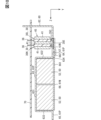
- FIG. 10 is a cross-sectional view corresponding to line XX in FIG. In FIG. 10, only the laminate 45, the capacitor element 52, the bus bar 60, and the circuit board 70 are shown for convenience.
- FIG. 11 is a plan view showing the arrangement of each bus bar 60. As shown in FIG. FIG. 11 corresponds to FIG. FIG. 12 shows the state before the extension portion 67 of the negative bus bar 61N is arranged, and FIG. 13 shows the state after the extension portion 67 is arranged. 12 and 13, for the sake of convenience, the extended portion 65 of the positive bus bar 61P and the extended portion 68 of the negative bus bar 61N are omitted.
- the busbar 60 is a wiring member electrically connected to the semiconductor module 30 .
- the busbar 60 is a plate-like metal member.
- the busbars 60 are connected to corresponding main terminals 35 by soldering, resistance welding, laser welding, or the like.
- the bus bar 60 includes a power bus bar 61 and an output bus bar 62. As shown in FIG.
- the power bus bar 61 electrically connects the semiconductor module 30 and the capacitor element 52 .
- the power busbar 61 includes a positive busbar 61P and a negative busbar 61N.
- Positive electrode bus bar 61P electrically connects each of collector terminals 35C (P terminals) of upper arm module 30H and the positive electrode of capacitor element 52 .
- the positive electrode busbar 61P is sometimes called a P busbar, a high-potential power busbar, or the like.
- the positive bus bar 61P constitutes at least part of the P line 8 described above.
- the positive busbar 61P corresponds to a second power busbar.
- the positive electrode busbar 61P has a base portion 63 and extension portions 64 and 65.
- Base 63 is connected to the positive electrode of capacitor element 52 .
- the base 63 is arranged inside the case 51 and includes a portion facing the bottom wall of the case 51 and the two side walls in the Z direction.
- the base portion 63 faces three surfaces of the entire capacitor element 52 having a substantially rectangular parallelepiped shape.
- the base portion 63 has a bottom facing portion 631 , side facing portions 632 and 633 , and a bent portion 634 .
- the bottom facing portion 631 faces the bottom of the capacitor element 52 .
- the side facing portion 632 faces the side surface of the capacitor element 52 on the laminate 45 side.
- the side facing portion 633 faces the side surface of the capacitor element 52 on the side opposite to the side facing portion 632 in the Z direction.
- the bent portion 634 is bent at an angle of approximately 90 degrees with respect to the side facing portion 632 .
- the bent portion 634 continues to the side facing portion 632 and extends from the side facing portion 632 in the Z direction toward the laminate 45 side.
- the bent portion 634 is arranged outside the case 51 .
- the extended portion 64 continues to the bent portion 634 of the base portion 63 and extends in the Z direction.
- the width of the extension portion 64 is narrower than the width of the base portion 63 .
- the positive bus bar 61P has three extensions 64 corresponding to each phase.
- the three extended portions 64 extend in the same direction from a common bent portion 634 .
- the three extensions 64 are arranged in the X direction.
- the plate thickness direction of the extension portion 64 is substantially parallel to the Y direction.
- the plate surface of the extension portion 64 faces the plate surface of the tip portion 353 of the collector terminal 35C of the upper arm module 30H. Further, the extending portion 64 and the collector terminal 35C of the upper arm module 30H are connected at the place where the plate surfaces face each other.
- Each of the extension portions 64 straddles (traverses) the first-stage heat exchange portion 41 in the Z direction.
- the extension part 65 is connected to the base part 63 on the side opposite to the extension part 64 .
- the extending portion 65 extends from the base portion 63 in the opposite direction to the extending portion 64 .
- the width of the extension portion 65 is narrower than the width of the base portion 63 .
- the extension part 65 constitutes a connector 80 for connecting with the DC power supply 2 .
- the extension 65 is the positive terminal of the connector 80 .
- the positive electrode bus bar 61P configured as described above may be formed, for example, by processing a single metal plate, or may be formed by connecting (joining) a plurality of members.
- the negative electrode bus bar 61N electrically connects each of the emitter terminals 35E (N terminal) of the lower arm module 30L and the negative electrode of the capacitor element 52.
- the negative bus bar 61N is sometimes called an N bus bar, a low potential power bus bar, or the like.
- the negative bus bar 61N constitutes at least part of the N line 9. As shown in FIG.
- the negative bus bar 61N corresponds to the first power bus bar.
- the negative electrode bus bar 61N has a base portion 66 and extension portions 67 and 68.
- Base 66 is connected to the negative electrode of capacitor element 52 . At least part of the base 66 is arranged outside the case 51 .
- the base portion 66 has a covering portion 661 and a facing portion 662 .
- the covering portion 661 is arranged so as to cover the entire capacitor element 52 having a substantially rectangular parallelepiped shape in plan view in the Y direction.
- Coating portion 661 faces the upper surface of capacitor element 52 and is connected to the negative electrode.
- the facing portion 662 continues to the covering portion 661 and extends toward the laminate 45 in the Z direction.
- the facing portion 662 is arranged so as to substantially match the bent portion 634 of the positive bus bar 61P in plan view in the Z direction.
- the plate thickness direction of the opposing portion 662 is substantially parallel to the Y direction.
- the width of the facing portion 662 is narrower than the width of the covering portion 661 in the X direction.
- the opposing portion 662 and the bent portion 634 of the positive bus bar 61P are opposed to each other with their plate surfaces separated from each other.
- the extended portion 67 is connected (joined) to the facing portion 662 of the base portion 66 .
- the extending portion 67 is provided separately from the base portion 66 and integrated by connection.
- the extended portion 67 includes a portion that continues to the base portion 66 and extends toward the laminated body 45 in the Z direction.
- the plate thickness direction of the extending portion 67 is substantially parallel to the Y direction.
- the plate surface of the extension portion 67 faces the plate surface of the tip portion 353 of the emitter terminal 35E of the lower arm module 30L. Further, the extending portion 67 and the emitter terminal 35E of the lower arm module 30L are connected at a location where the plate surfaces face each other.
- the extended portion 67 is arranged to cover the projecting portion of the main terminal 35 , at least part of the extended portion 64 of the positive electrode busbar 61 ⁇ /b>P, and at least part of the output busbar 62 .
- the extended portion 67 straddles (traverses) the first-stage heat exchange portion 41 and the second-stage heat exchange portion 41 in the Z direction.
- the extended portion 67 has a slit 671, a parallel running portion 672, a facing portion 673, and a connecting portion 674.
- the slit 671 is provided between the upper arm module 30H and the lower arm module 30L in plan view in the Y direction.
- the slit 671 is provided between the collector terminal 35C of the upper arm module 30H and the emitter terminal 35E of the lower arm module 30L.
- the slit 671 may be referred to as a notch.
- the extending portion 67 has slits 671 for three phases.
- the three slits 671 are arranged side by side in the X direction.
- the parallel running portion 672 has a portion adjacent to the slit 671 in the X direction.
- the parallel running portion 672 defines a slit 671 .
- At least part of the parallel running portion 672 runs parallel to the output bus bar 62 .
- the plate surfaces of the parallel running portion 672 and the output bus bar 62 face each other with a gap therebetween.
- the parallel running portion 672 extends in the Z direction and maintains a facing relationship with the output bus bar 62 in the extending direction.
- the extension portion 67 has parallel running portions 672 for three phases.
- the three parallel running portions 672 are arranged side by side in the X direction.
- the facing portion 673 has a portion adjacent to the slit on the capacitor module 50 side in the Z direction.
- the facing portion 673 defines the slit 671 .
- the facing portion 673 extends from the parallel running portion 672 in the X direction.
- the facing portion 673 and the extending portion 64 of the positive bus bar 61P face each other with their plate surfaces separated from each other.
- the facing portion 673 maintains a facing relationship with the extending portion 64 over the entire length of the extending portion 64, for example.
- the connecting portion 674 is adjacent to the slit 671 on the side opposite to the facing portion 673 in the Z direction.
- the connecting portion 674 defines the slit 671 .
- the connecting portion 674 extends from the parallel running portion 672 in the X direction.
- the plate surface of the connecting portion 674 faces the plate surface of the tip portion 353 of the emitter terminal 35E of the lower arm module 30L.
- the connection portion 674 and the emitter terminal 35E of the lower arm module 30L are connected at a location where the plate surfaces face each other.
- the extended portion 68 continues to the base portion 66 on the side opposite to the extended portion 67 .
- the extending portion 68 extends from the base portion 66 in the direction opposite to the extending portion 67 .
- the width of the extension portion 68 is narrower than the width of the base portion 66 .
- the extended portion 68 is aligned with the extended portion 65 of the positive bus bar 61P in the X direction.
- the extending portion 68 constitutes a connector 80 .
- the extension 68 is the negative terminal of the connector 80 .
- the connector 80 includes extensions 65 and 68 and a portion of the case 51 .
- the connector 80 is sometimes called an input terminal block.
- the output bus bar 62 electrically connects the emitter terminal 35E of the upper arm module 30H and the collector terminal 35C of the lower arm module 30L.
- the output bus bar 62 has a portion extending away from the capacitor module 50 in the Z direction.
- the plate surface of the output bus bar 62 faces the plate surface of the tip portion 353 of the emitter terminal 35E of the upper arm module 30H and the plate surface of the tip portion 353 of the collector terminal 35C of the lower arm module 30L.
- the output bus bar 62 and the distal end portion 353 are connected to each other at locations where the plate surfaces face each other.
- the busbar 60 includes output busbars 62 for three phases.
- the plate surfaces of the U-phase output bus bar 62 (U) and one of the parallel running portions 672 face each other.
- the plate surfaces of the V-phase output bus bar 62 (V) and the other one of the parallel running portions 672 face each other.
- the plate surfaces of the W-phase output bus bar 62 (W) and the other one of the parallel running portions 672 face each other.
- Each of the output bus bars 62 straddles (traverses) the second stage heat exchange section 41 and the third stage heat exchange section 41 in the Z direction.
- One end of each output bus bar 62 protrudes outside from an opening of case 20 so as to be connectable to motor generator 3 .
- a current sensor 81 is provided in the middle of the output bus bar 62 .
- a current sensor 81 is provided individually for each output bus bar 62 .
- a current sensor 81 detects a phase current.
- the current sensor 81 is arranged inside the case 20 .
- the extended portion 67 of the negative electrode bus bar 61N is provided separately from the base portion 66.
- the extended portion 64 of the positive electrode bus bar 61P is connected to the collector terminal 35C(P) of the upper arm module 30H
- the output bus bar 62 is connected to the emitter terminal 35E(O) of the upper arm module 30H and the lower arm module 30L. Connect to the collector terminal 35C(O).
- the busbars 60 on the upper layer side in the Z direction are connected to the corresponding main terminals 35 .
- the extended portion 67 of the negative bus bar 61N is connected to the base portion 66 and connected to the emitter terminal 35E(N) of the lower arm module 30L.
- the parallel running structure of the negative electrode bus bar 61N and the positive electrode bus bar 61P and the parallel running structure of the negative electrode bus bar 61N and the output bus bar 62 can be realized.
- the circuit board 70 includes a wiring board in which wiring is arranged on an insulating base material such as resin, and electronic components (not shown) mounted on the wiring board. Wiring and electronic components make up a circuit.
- the drive circuit 7 described above is configured on the circuit board 70 .
- the circuit board 70 has a connector 71 for connection with an external device.
- the connector 71 includes a housing molded using resin or the like, and terminals held by the housing and mounted on a wiring board. For convenience, the terminals are simplified or omitted in each drawing.
- a drive command for the control circuit is input via the connector 71 .
- a torque request is input from the host ECU via the connector 71 .
- the circuit board 70 is arranged on the opening side of the case 20 in the Z direction. Circuit board 70 is arranged such that capacitor module 50 and laminate 45 are positioned between bottom wall 21 of case 20 and circuit board 70 . The circuit board 70 is arranged so as to overlap with the capacitor module 50 and the laminate 45 in plan view in the Y direction. Signal terminals 36 of the semiconductor module 30 included in the laminate 45 are inserted and mounted on the circuit board 70 . A surface mounting structure may be adopted instead of insertion mounting.
- the circuit board 70 has through holes (not shown) for projecting the output busbars 62 out of the case 20 .
- FIG. 14 shows the PN current loop in this embodiment.
- a PN current loop which is a current path from the collector terminal 35C of the upper arm module 30H, which is the P terminal, to the emitter terminal 35E of the lower arm module 30L, which is the N terminal, is considered.
- the dashed line indicates the current path from the collector terminal 35C(P) of the upper arm module 30H to the emitter terminal 35E(O).
- N) is indicated by a solid line.
- each semiconductor element 32 is controlled so that the semiconductor element 32 of the upper arm module 30H and the semiconductor element 32 of the lower arm module 30L that constitute the upper and lower arm circuits 10 are not turned on at the same time.
- the plurality of semiconductor modules 30 are divided into upper arm modules 30H and lower arm modules 30L.
- the upper arm module 30H and the lower arm module 30L are arranged side by side in the Z direction (stacking direction). This makes it possible to reduce the PN current loop compared to a configuration in which one module provides upper and lower arm circuits for one phase and a configuration in which the upper arm module and the lower arm module are arranged in the X direction. Smaller PN current loops can reduce inductance because opposing current-carrying members are closer together, increasing flux cancellation.
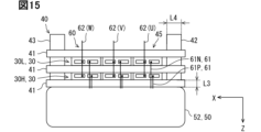
- FIG. 15 shows the arrangement of semiconductor modules 30, coolers 40, and capacitor modules 50 in this embodiment.
- the capacitor modules 50 are arranged in the Z direction with respect to the laminate 45 .
- the power supply bus bar 61 extends in the Z direction so as to straddle at least one of the heat exchange sections 41 arranged in multiple stages.
- the length L3 for one stage of the heat exchange section 41 is sufficiently shorter than the length L4 equal to the diameter of the pipe. Therefore, the length of the power bus bar 61 can be shortened compared to a configuration in which the capacitor modules are arranged next to the laminate in the X direction and the power bus bar extends in the X direction so as to straddle one of the pipes. That is, the current path can be shortened.
- the power conversion device 4 of this embodiment can reduce the inductance.
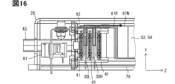
- FIG. 16 shows the current paths of the main circuit including smoothing capacitor 5 and inverter 6 .
- the lower arm module 30L is arranged further away from the capacitor module 50 than the upper arm module 30H.
- the negative bus bar 61N and the positive bus bar 61P extend in the Z direction with their plate surfaces facing each other.
- the negative electrode bus bar 61N and the output bus bar 62 extend in the Z direction with their plate surfaces facing each other.
- Negative bus bar 61N may be arranged to face at least one of positive bus bar 61P and output bus bar 62 .
- a plurality of upper arm modules 30H forming the three-phase upper and lower arm circuits 10 are arranged side by side in the X direction orthogonal to the Z direction.
- lower arm modules 30L are arranged side by side in the X direction.
- the upper arm module 30H and the lower arm module 30L may be arranged such that the arrangement of the collector terminals 35C and the emitter terminals 35E are the same.
- the lower arm module 30L is arranged such that the front and back surfaces of the semiconductor element 32 are reversed with respect to the upper arm module 30H.
- the arrangement of the collector terminal 35C and the emitter terminal 35E is reversed, so that the emitter terminal 35E of the upper arm module 30H and the collector terminal 35C of the lower arm module 30L can be easily connected by the output bus bar 62.
- the shape of the projecting portion of the main terminal 35 is not particularly limited.
- the entire projecting portion may have a shape extending in the Y direction.
- the projecting portions of the plurality of main terminals 35 each have a bent portion 351 .
- a plate surface of tip portion 353 which is a portion closer to the projecting tip than the bent portion, faces the corresponding plate surface of bus bar 60 .
- the presence of the bent portion 351 shortens the distance to the bus bar 60 to be joined, thereby further reducing the inductance.
- connection processing such as welding is easy to perform.
- the length L1 of the root portion 352 is shorter than the length L2 of the tip portion 353 at the projecting portion of each main terminal 35 . That is, inductance can be reduced more effectively.
- the extension portion 67 of the negative electrode bus bar 61N may be continuously connected to the base portion 66.
- the extended portion 67 is provided separately from the base portion 66 and integrated by joining. According to this, as shown in FIGS. 12 and 13 , the lower layer positive bus bar 61P and the output bus bar 62 can be joined to the corresponding main terminals 35 before joining the extended portion 67 . In other words, the connection between the busbar 60 and the corresponding main terminal 35 is facilitated.
- the extension portion 67 may have, for example, a substantially rectangular shape in a plan view in the Y direction so as to integrally cover portions of the main terminal 35, the extension portion 64 of the negative bus bar 61N, and the output bus bar 62. .
- FIG. 17 shows current paths in the main circuit.
- FIG. 17 corresponds to FIG.
- FIG. 17 shows a U-phase current path as an example.
- the solid line arrow indicates the path in the extended portion 67 of the negative bus bar 61N
- the broken line arrow indicates the path from the extended portion 64 of the positive bus bar 61P to the emitter terminal 35E(N) of the lower arm module 30L.
- the extended portion 67 of the negative bus bar 61N of the present embodiment has a slit 671, a parallel running portion 672, a facing portion 673, and a connecting portion 674.
- the slit 671 in this manner, the current path in the negative bus bar 61N (extended portion 67) is restricted. Specifically, current flows along the slit 671 . Therefore, as shown in FIG. 17, the parallel running distance in the current path can be increased. Thereby, the effect of canceling the magnetic flux can be enhanced and the inductance can be further reduced.
- the connecting portion 674 can be easily bent with respect to other portions of the extending portion 67 so as to be joined to the emitter terminal 35E(N). In other words, the connection between the emitter terminal 35E of the lower arm module 30L and the extended portion 67 is facilitated.
- the present invention is not limited to this.
- the lower arm module 30L may be arranged on the capacitor module 50 side.
- the upper arm module 30H corresponds to the first semiconductor module
- the lower arm module 30L closer to the capacitor module 50 than the upper arm module 30H corresponds to the second semiconductor module.
- the positive bus bar 61P corresponds to a first power bus bar
- the negative bus bar 61N corresponds to a second power bus bar.
- the extended portion of the positive electrode bus bar 61P is at least part of the projected portion of the main terminal 35, at least part of the extended portion of the negative electrode bus bar 61N, and the extended portion of the output bus bar 62. It is good also as arrangement
- the extending portion of the positive electrode bus bar 61P may be provided separately from the base portion. A slit or the like may be provided in the extended portion of the positive electrode bus bar 61P to increase the parallel running distance.
- the present invention is not limited to this.
- the upper arm 10H for three phases may be provided by one upper arm module 30H by sharing the sealing body 31 so as to integrally seal the semiconductor elements 32 for three phases.
- the lower arm 10L for three phases may be provided by one lower arm module 30L.
- one semiconductor element 32 constitutes one arm 10H, 10L.
- a plurality of semiconductor elements 32 may be connected in parallel to form one arm 10H, 10L.
- FIG. 18 is a diagram showing the circuit configuration of the power conversion device 4 according to this embodiment.
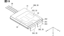
- 19 is a perspective view showing the semiconductor module 30.
- FIG. FIG. 19 corresponds to FIG. 6 and shows the upper arm module 30H as an example.
- each arm 10H, 10L of the upper and lower arm circuits 10 forming the inverter 6 is configured by connecting two IGBTs 12 in parallel.
- the two IGBTs 12 connected in parallel are controlled by a gate drive signal that switches between high level and low level at the same timing.
- the FWD 13 is connected in anti-parallel to each of the IGBTs 12 .
- the semiconductor module 30 includes two semiconductor elements 32. As shown in FIG. Each semiconductor element 32 is formed with an RC-IGBT as in the previous embodiment. The two semiconductor elements 32 are arranged side by side in the X direction. The collector electrodes 32C of the two semiconductor elements 32 are electrically connected to a common collector terminal 35C via the surface metal bodies 332 (wiring portions 334). The emitter electrodes 32E of the two semiconductor elements 32 are electrically connected to a common emitter terminal 35E via the surface metal body 342 (wiring portion 344).
- the power conversion device 4 of this embodiment has the same configuration as the power conversion device 4 shown in the preceding embodiment, except that the semiconductor module 30 includes a plurality of semiconductor elements 32 .
- a laminated body 45 is configured by the heat exchange units arranged in three stages and the semiconductor modules 30 arranged in two stages.
- the upper arm module 30H and the lower arm module 30L are arranged side by side in the Z direction. Any of the configurations shown in the previous embodiment and its modification can be applied to the power conversion device 4 of the present embodiment. Therefore, the power conversion device 4 of this embodiment can achieve the same effect as the power conversion device 4 of the preceding embodiment.
- the number of switching elements forming one arm 10H, 10L is not limited to two. It may be three or more.
- the number of semiconductor elements 32 included in the semiconductor module 30 is also not limited to two. It may be three or more.
- One semiconductor module 30 provides a parallel circuit of one arm 10H, 10L.
- multiple semiconductor modules 30 may provide a parallel circuit.
- FIG. 20 shows the arrangement of the laminate 45 and the busbars 60 in the power conversion device 4 according to this embodiment.
- FIG. 20 corresponds to FIG.
- FIG. 21 shows the state before the extension portion 67 of the negative bus bar 61N is arranged
- FIG. 22 shows the state after the extension portion 67 is arranged.
- 21 and 22 correspond to FIGS. 12 and 13.
- each semiconductor module 30 has a configuration similar to that of the first embodiment (see FIGS. 6 and 7). That is, one semiconductor module 30 has one semiconductor element 32 . Although illustration is omitted, each arm 10H, 10L of the upper and lower arm circuit 10 is configured by connecting three IGBTs 12 in parallel.
- the laminate 45 includes semiconductor modules 30 arranged in six stages and heat exchange sections 41 arranged in seven stages.
- the three semiconductor modules 30 closer to the capacitor module 50 in the Z direction are the upper arm modules 30H, and the three semiconductor modules 30 farther are the lower arm modules 30L.
- the upper arm modules 30H are arranged in the X direction in the order of U-phase, V-phase, and W-phase in each stage.
- the extended portion 64 of the positive bus bar 61P extends in the Z direction and is electrically connected to the three collector terminals 35C(P) of the corresponding phases.
- the lower arm modules 30L are also arranged in the X direction in the order of U-phase, V-phase, and W-phase in each stage.
- the output bus bar 62 extends in the Z direction and is electrically connected to the main terminal 35 of the corresponding phase, specifically the emitter terminal 35E(O) of the upper arm module 30H and the collector terminal 35C(O) of the lower arm module 30L. It is
- the extending portion 67 of the negative electrode bus bar 61N has a slit 671, a parallel running portion 672, a facing portion 673, and a connecting portion 674, as in the previous embodiment.
- a slit 671 is provided between the upper arm module 30H and the lower arm module 30L in each phase.
- the slit 671 is provided between the collector terminal 35C(P) and the emitter terminal 35E(N).
- the parallel running portion 672 is provided so as to overlap the connection portion of the output bus bar 62 with the main terminal 35 in plan view in the Z direction so that the output bus bar 62 and the plate surfaces face each other.
- the opposing portion 673 extends in the X direction from the parallel running portion 672 and is provided so as to overlap the extended portion 64 of the positive electrode bus bar 61P.
- the connecting portion 674 extends in the X direction from the parallel running portion 672 and is electrically connected to the emitter terminal 35E(N) of the lower arm module 30L.
- the three upper arm modules 30H of the same phase are connected in parallel by the busbars 61P and 62.
- Three lower arm modules 30L of the same phase are connected in parallel by bus bars 61N and 62 .
- the extended portion 67 of this embodiment is also provided separately from the base portion 66 .
- connection (bonding) of the busbars 60 first, as shown in FIG. 21 , the busbars 60 on the lower layer side in the Z direction are connected to the corresponding main terminals 35 .
- the extended portion 64 of the positive electrode bus bar 61P is connected to the collector terminal 35C(P) of the upper arm module 30H
- the output bus bar 62 is connected to the emitter terminal 35E(O) of the upper arm module 30H and the lower arm module 30L. Connect to the collector terminal 35C(O).
- the busbars 60 on the upper layer side in the Z direction are connected to the corresponding main terminals 35 .
- the extended portion 67 of the negative bus bar 61N is connected to the base portion 66 and connected to the emitter terminal 35E(N) of the lower arm module 30L.
- the parallel running structure of the negative electrode bus bar 61N and the positive electrode bus bar 61P and the parallel running structure of the negative electrode bus bar 61N and the output bus bar 62 can be realized.
- the power conversion device 4 of this embodiment has the same configuration as the power conversion device 4 shown in the first embodiment, except that a plurality of semiconductor modules 30 are connected in parallel by bus bars 60 .
- a plurality of semiconductor modules 30 are divided into upper arm modules 30H and lower arm modules 30L, and the upper arm modules 30H and lower arm modules 30L are arranged side by side in the Z direction. This makes it possible to reduce the PN current loop.
- the capacitor module 50 is arranged in the Z direction with respect to the laminate 45 .
- the power supply bus bar 61 extends in the Z direction so as to straddle at least one of the heat exchange sections 41 arranged in multiple stages. Thereby, the length of the power bus bar 61 can be shortened. Therefore, inductance can be reduced.
- the number of switching elements forming one arm 10H, 10L is not limited to three. It may be two, or four or more.
- the number of semiconductor modules 30 is not limited to three. It may be two, or four or more.
- spatially relative terms “inside”, “outside”, “behind”, “below”, “low”, “above”, “high”, etc. refer to an element or feature as illustrated. It is used here to facilitate the description describing its relationship to other elements or features. Spatially-relative terms can be intended to encompass different orientations of the device in use or operation in addition to the orientation depicted in the drawings. For example, when the device in the figures is turned over, elements described as “below” or “beneath” other elements or features are oriented “above” the other elements or features. Thus, the term “bottom” can encompass both an orientation of up and down. The device may be oriented in other directions (rotated 90 degrees or other orientations) and the spatially relative descriptors used herein interpreted accordingly. .
- the vehicle drive system 1 is not limited to the configuration described above.
- the example provided with one motor generator 3 was shown, it is not limited to this. A plurality of motor generators may be provided.
- the present invention is not limited to this.
- the configuration may include a plurality of inverters. At least one inverter and a converter may be provided. Only a converter may be provided.
Abstract
A plurality of semiconductor modules (30) include an upper arm module (30H) and a lower arm module (30L) disposed in line with the upper arm module in the lamination direction. Heat exchange units (41) of a cooler (40) are disposed in multiple stages in the lamination direction so as to cool the upper arm module and the lower arm module from both surface sides, and form a laminate (45) together with the semiconductor module. A capacitor module (50) is disposed on one end side of the laminate in the lamination direction. A power supply bus bar (61) for electrically connecting the capacitor module and the semiconductor module extends in the lamination direction so as to straddle at least one of the heat exchange units.
Description
この出願は、2021年10月6日に日本に出願された特許出願第2021-165000号を基礎としており、基礎の出願の内容を、全体的に、参照により援用している。
This application is based on Patent Application No. 2021-165000 filed in Japan on October 6, 2021, and the content of the underlying application is incorporated by reference in its entirety.
この明細書における開示は、電力変換装置に関する。
The disclosure in this specification relates to a power converter.
特許文献1は、電力変換装置を開示している。この電力変換装置は、複数の半導体モジュールと、冷却器と、コンデンサと、複数のバスバーを備えている。冷却器は、半導体モジュールのそれぞれを両面側から挟むように多段に配置された複数の熱交換部を有している。複数のバスバーは、コンデンサと半導体モジュールとを電気的に接続する電源バスバーを含んでいる。先行技術文献の記載内容は、この明細書における技術的要素の説明として、参照により援用される。
Patent Document 1 discloses a power converter. This power converter includes a plurality of semiconductor modules, a cooler, a condenser, and a plurality of busbars. The cooler has a plurality of heat exchanging portions arranged in multiple stages so as to sandwich each of the semiconductor modules from both sides. The plurality of busbars includes power busbars electrically connecting the capacitors and the semiconductor modules. The contents of the prior art documents are incorporated by reference as descriptions of technical elements in this specification.
特許文献1では、半導体モジュールのそれぞれが、一相分の上下アーム回路を構成している。このような半導体モジュールは、内部に上アームを構成する半導体素子と下アームを構成する半導体素子を有しており、これら半導体素子は積層方向に直交する一方向に並んで配置されている。このため、半導体モジュール内においてPN電流ループが大きくなる。また、コンデンサが、半導体モジュールと熱交換部との積層体に対して、積層方向に直交する一方向に配置されている。半導体モジュールとコンデンサとの間には、熱交換部に対して冷媒を導入または排出するパイプが配置されている。このため、冷却器のパイプを跨いで電源バスバーを配策しなければならず、電源バスバーが長くなる。上記した観点において、または言及されていない他の観点において、電力変換装置にはさらなる改良が求められている。
In Patent Document 1, each semiconductor module constitutes an upper and lower arm circuit for one phase. Such a semiconductor module has therein a semiconductor element forming an upper arm and a semiconductor element forming a lower arm, and these semiconductor elements are arranged side by side in one direction orthogonal to the stacking direction. As a result, the PN current loop becomes large within the semiconductor module. Also, the capacitor is arranged in one direction orthogonal to the stacking direction with respect to the stack of the semiconductor module and the heat exchange portion. A pipe is arranged between the semiconductor module and the condenser to introduce or discharge the refrigerant to or from the heat exchange section. Therefore, the power bus bar must be routed across the pipes of the cooler, resulting in a long power bus bar. Further improvements are required for the power conversion device from the above viewpoints or from other viewpoints not mentioned.
開示されるひとつの目的は、インダクタンスを低減できる電力変換装置を提供することにある。
One object of the disclosure is to provide a power conversion device capable of reducing inductance.
ここに開示された電力変換装置は、
上下アーム回路の上アームを構成する上アームモジュールと、上下アーム回路の下アームを構成し、上アームモジュールと積層方向に並んで配置された下アームモジュールと、を含む複数の半導体モジュールと、
積層方向において上アームモジュールおよび下アームモジュールのそれぞれを両面側から冷却するように多段に配置され、複数の半導体モジュールとともに積層体をなす複数の熱交換部を有する冷却器と、
積層方向において積層体の一端側に配置されたコンデンサと、
コンデンサと半導体モジュールとを電気的に接続し、熱交換部の少なくともひとつを跨ぐように積層方向に延びた電源バスバーを含む複数のバスバーと、を備える。 The power conversion device disclosed here is
a plurality of semiconductor modules including an upper arm module forming an upper arm of the upper and lower arm circuits, and a lower arm module forming a lower arm of the upper and lower arm circuits and arranged side by side with the upper arm modules in the stacking direction;
a cooler having a plurality of heat exchange portions arranged in multiple stages so as to cool the upper arm module and the lower arm module from both sides in the stacking direction and forming a laminate together with the plurality of semiconductor modules;
a capacitor arranged on one end side of the laminate in the lamination direction;
a plurality of bus bars including a power supply bus bar that electrically connects the capacitor and the semiconductor module and extends in the stacking direction so as to straddle at least one of the heat exchanging parts.
開示された電力変換装置によれば、複数の半導体モジュールを上アームモジュールと下アームモジュールとに分けるとともに、上アームモジュールと下アームモジュールとを積層方向に並ぶ配置としている。これにより、PN電流ループを小さくすることができる。また、コンデンサを積層体に対して積層方向に配置し、電源バスバーを熱交換部の少なくともひとつを跨ぐように積層方向に延設している。これにより、電源バスバー長、つまり電流経路を短くすることができる。この結果、インダクタンスを低減できる電力変換装置を提供することができる。
According to the disclosed power converter, a plurality of semiconductor modules are divided into upper arm modules and lower arm modules, and the upper arm modules and lower arm modules are arranged side by side in the stacking direction. This makes it possible to reduce the PN current loop. Also, the capacitors are arranged in the stacking direction with respect to the stack, and the power supply bus bar is extended in the stacking direction so as to straddle at least one of the heat exchange portions. As a result, the length of the power busbar, that is, the current path can be shortened. As a result, it is possible to provide a power conversion device capable of reducing inductance.
この明細書における開示された複数の態様は、それぞれの目的を達成するために、互いに異なる技術的手段を採用する。請求の範囲およびこの項に記載した括弧内の符号は、後述する実施形態の部分との対応関係を例示的に示すものであって、技術的範囲を限定することを意図するものではない。この明細書に開示される目的、特徴、および効果は、後続の詳細な説明、および添付の図面を参照することによってより明確になる。
The multiple aspects disclosed in this specification employ different technical means in order to achieve their respective objectives. Reference numerals in parentheses described in the claims and this section are intended to exemplify the correspondence with portions of the embodiments described later, and are not intended to limit the technical scope. Objects, features, and advantages disclosed in this specification will become clearer with reference to the following detailed description and accompanying drawings.
以下、図面に基づいて複数の実施形態を説明する。なお、各実施形態において対応する構成要素には同一の符号を付すことにより、重複する説明を省略する場合がある。各実施形態において構成の一部分のみを説明している場合、当該構成の他の部分については、先行して説明した他の実施形態の構成を適用することができる。また、各実施形態の説明において明示している構成の組み合わせばかりではなく、特に組み合わせに支障が生じなければ、明示していなくても複数の実施形態の構成同士を部分的に組み合せることができる。
A plurality of embodiments will be described below based on the drawings. Note that redundant description may be omitted by assigning the same reference numerals to corresponding components in each embodiment. When only a part of the configuration is described in each embodiment, the configurations of other embodiments previously described can be applied to other portions of the configuration. In addition, not only the combinations of the configurations specified in the description of each embodiment, but also the configurations of a plurality of embodiments can be partially combined even if they are not specified unless there is a particular problem with the combination. .
本実施形態の電力変換装置は、たとえば、回転電機を駆動源とする移動体に適用される。移動体は、たとえば、電気自動車(BEV)、ハイブリッド自動車(HEV)、プラグインハイブリッド自動車(PHEV)などの電動車両、ドローンなどの飛行体、船舶、建設機械、農業機械である。以下では、車両に適用される例について説明する。
The power conversion device of this embodiment is applied, for example, to a moving body that uses a rotating electric machine as a drive source. Mobile objects include, for example, electric vehicles such as electric vehicles (BEV), hybrid vehicles (HEV), and plug-in hybrid vehicles (PHEV), flying vehicles such as drones, ships, construction machinery, and agricultural machinery. An example applied to a vehicle will be described below.
(第1実施形態)
まず、図1に基づき、車両の駆動システムの概略構成について説明する。 (First embodiment)
First, based on FIG. 1, a schematic configuration of a vehicle drive system will be described.
まず、図1に基づき、車両の駆動システムの概略構成について説明する。 (First embodiment)
First, based on FIG. 1, a schematic configuration of a vehicle drive system will be described.
<車両の駆動システム>
図1に示すように、車両の駆動システム1は、直流電源2と、モータジェネレータ3と、電力変換装置4を備えている。 <Vehicle drive system>
As shown in FIG. 1 , avehicle drive system 1 includes a DC power supply 2 , a motor generator 3 , and a power conversion device 4 .
図1に示すように、車両の駆動システム1は、直流電源2と、モータジェネレータ3と、電力変換装置4を備えている。 <Vehicle drive system>
As shown in FIG. 1 , a
直流電源2は、充放電可能な二次電池で構成された直流電圧源である。二次電池は、たとえばリチウムイオン電池、ニッケル水素電池である。モータジェネレータ3は、三相交流方式の回転電機である。モータジェネレータ3は、車両の走行駆動源、つまり電動機として機能する。モータジェネレータ3は、回生時に発電機として機能する。電力変換装置4は、直流電源2とモータジェネレータ3との間で電力変換を行う。
The DC power supply 2 is a DC voltage source composed of a rechargeable secondary battery. Secondary batteries are, for example, lithium ion batteries and nickel metal hydride batteries. The motor generator 3 is a three-phase alternating-current rotating electric machine. The motor generator 3 functions as a vehicle drive source, that is, as an electric motor. The motor generator 3 functions as a generator during regeneration. The power converter 4 performs power conversion between the DC power supply 2 and the motor generator 3 .
<電力変換装置の回路構成>
図1は、電力変換装置4の回路構成を示している。電力変換装置4は、電力変換回路を備えている。本実施形態の電力変換装置4は、平滑コンデンサ5と、電力変換回路であるインバータ6と、駆動回路7を備えている。 <Circuit Configuration of Power Converter>
FIG. 1 shows the circuit configuration of thepower conversion device 4. As shown in FIG. The power conversion device 4 includes a power conversion circuit. The power conversion device 4 of this embodiment includes a smoothing capacitor 5 , an inverter 6 that is a power conversion circuit, and a drive circuit 7 .
図1は、電力変換装置4の回路構成を示している。電力変換装置4は、電力変換回路を備えている。本実施形態の電力変換装置4は、平滑コンデンサ5と、電力変換回路であるインバータ6と、駆動回路7を備えている。 <Circuit Configuration of Power Converter>
FIG. 1 shows the circuit configuration of the
平滑コンデンサ5は、主として、直流電源2から供給される直流電圧を平滑化する。平滑コンデンサ5は、高電位側の電源ラインであるPライン8と低電位側の電源ラインであるNライン9とに接続されている。Pライン8は直流電源2の正極に接続され、Nライン9は直流電源2の負極に接続されている。平滑コンデンサ5の正極は、直流電源2とインバータ6との間において、Pライン8に接続されている。平滑コンデンサ5の負極は、直流電源2とインバータ6との間において、Nライン9に接続されている。平滑コンデンサ5は、直流電源2に並列に接続されている。
The smoothing capacitor 5 mainly smoothes the DC voltage supplied from the DC power supply 2 . The smoothing capacitor 5 is connected to a P line 8 that is a power supply line on the high potential side and an N line 9 that is a power supply line on the low potential side. The P line 8 is connected to the positive pole of the DC power supply 2 and the N line 9 is connected to the negative pole of the DC power supply 2 . The positive terminal of smoothing capacitor 5 is connected to P line 8 between DC power supply 2 and inverter 6 . The negative electrode of smoothing capacitor 5 is connected to N line 9 between DC power supply 2 and inverter 6 . A smoothing capacitor 5 is connected in parallel with the DC power supply 2 .
インバータ6は、DC-AC変換回路である。インバータ6は、図示しない制御回路によるスイッチング制御にしたがって、直流電圧を三相交流電圧に変換し、モータジェネレータ3へ出力する。これにより、モータジェネレータ3は、所定のトルクを発生するように駆動する。インバータ6は、車両の回生制動時、車輪からの回転力を受けてモータジェネレータ3が発電した三相交流電圧を、制御回路によるスイッチング制御にしたがって直流電圧に変換し、Pライン8へ出力する。このように、インバータ6は、直流電源2とモータジェネレータ3との間で双方向の電力変換を行う。
The inverter 6 is a DC-AC conversion circuit. Inverter 6 converts the DC voltage into a three-phase AC voltage and outputs it to motor generator 3 according to switching control by a control circuit (not shown). Thereby, the motor generator 3 is driven to generate a predetermined torque. During regenerative braking of the vehicle, inverter 6 converts the three-phase AC voltage generated by motor generator 3 by receiving torque from the wheels into DC voltage according to switching control by the control circuit, and outputs the DC voltage to P line 8 . Thus, inverter 6 performs bidirectional power conversion between DC power supply 2 and motor generator 3 .
インバータ6は、三相分の上下アーム回路10を備えて構成されている。上下アーム回路10は、レグと称されることがある。上下アーム回路10は、上アーム10Hと、下アーム10Lをそれぞれ有している。以下では、上アーム10H、下アーム10Lを単にアーム10H、10Lと示すことがある。上アーム10Hおよび下アーム10Lは、上アーム10HをPライン8側として、Pライン8とNライン9との間で直列接続されている。上アーム10Hと下アーム10Lとの接続点は、出力ライン11を介して、モータジェネレータ3における対応する相の巻線3aに接続されている。インバータ6は、6つのアーム10H、10Lを有している。各アーム10H、10Lは、スイッチング素子を備えて構成されている。
The inverter 6 is configured with upper and lower arm circuits 10 for three phases. The upper and lower arm circuits 10 are sometimes called legs. The upper and lower arm circuits 10 each have an upper arm 10H and a lower arm 10L. Hereinafter, the upper arm 10H and the lower arm 10L may be simply referred to as arms 10H and 10L. The upper arm 10H and the lower arm 10L are connected in series between the P line 8 and the N line 9 with the upper arm 10H on the P line 8 side. A connection point between the upper arm 10H and the lower arm 10L is connected to a corresponding phase winding 3a in the motor generator 3 via an output line 11. FIG. The inverter 6 has six arms 10H and 10L. Each arm 10H, 10L is configured with a switching element.
本実施形態では、各アーム10H、10Lを構成するスイッチング素子として、nチャネル型の絶縁ゲートバイポーラトランジスタ12(以下、IGBT12と示す)を採用している。IGBTは、Insulated Gate Bipolar Transistorの略称である。IGBT12のそれぞれには、還流用のダイオード13(以下、FWD13と示す)が逆並列に接続されている。
In this embodiment, an n-channel insulated gate bipolar transistor 12 (hereinafter referred to as IGBT 12) is employed as a switching element forming each arm 10H, 10L. IGBT is an abbreviation for Insulated Gate Bipolar Transistor. A freewheeling diode 13 (hereinafter referred to as FWD 13) is connected in anti-parallel to each of the IGBTs 12 .
上アーム10Hにおいて、IGBT12のコレクタが、Pライン8に接続されている。下アーム10Lにおいて、IGBT12のエミッタが、Nライン9に接続されている。そして、上アーム10HにおけるIGBT12のエミッタと、下アーム10LにおけるIGBT12のコレクタが相互に接続されている。FWD13のアノードは対応するIGBT12のエミッタに接続され、カソードはコレクタに接続されている。
The collector of the IGBT 12 is connected to the P line 8 in the upper arm 10H. The emitter of IGBT 12 is connected to N line 9 in lower arm 10L. The emitter of IGBT 12 in upper arm 10H and the collector of IGBT 12 in lower arm 10L are connected to each other. The anode of FWD 13 is connected to the corresponding emitter of IGBT 12, and the cathode is connected to the collector.
なお、スイッチング素子は、IGBT12に限定されない。たとえばMOSFETを採用してもよい。MOSFETは、Metal Oxide Semiconductor Field Effect Transistorの略称である。MOSFETの場合、還流用のダイオードとして寄生ダイオード(ボディダイオード)を用いてもよいし、外付けのダイオードを用いてもよい。
It should be noted that the switching element is not limited to the IGBT 12. For example, a MOSFET may be employed. MOSFET is an abbreviation for Metal Oxide Semiconductor Field Effect Transistor. In the case of MOSFET, a parasitic diode (body diode) may be used as a freewheeling diode, or an external diode may be used.
駆動回路7は、インバータ6などの電力変換回路を構成するスイッチング素子を駆動する。駆動回路7は、制御回路の駆動指令に基づいて、対応するアーム10H、10LのIGBT12のゲートに駆動電圧を供給する。駆動回路は、駆動電圧の印加により、対応するIGBT12を駆動、すなわちオン駆動、オフ駆動させる。駆動回路は、ドライバと称されることがある。
The drive circuit 7 drives switching elements that make up a power conversion circuit such as the inverter 6 . The drive circuit 7 supplies a drive voltage to the gates of the IGBTs 12 of the corresponding arms 10H and 10L based on drive commands from the control circuit. The drive circuit drives the corresponding IGBT 12 by applying a drive voltage, that is, ON drive and OFF drive. A driving circuit is sometimes referred to as a driver.
電力変換装置4は、スイッチング素子の制御回路を備えてもよい。制御回路は、IGBT12を動作させるための駆動指令を生成し、駆動回路7に出力する。制御回路は、たとえば図示しない上位ECUから入力されるトルク要求、各種センサにて検出された信号に基づいて、駆動指令を生成する。ECUは、Electronic Control Unitの略称である。制御回路は、上位ECU内に設けてもよい。
The power conversion device 4 may include a control circuit for switching elements. The control circuit generates a drive command for operating the IGBT 12 and outputs it to the drive circuit 7 . The control circuit generates a drive command based on, for example, a torque request input from a host ECU (not shown) and signals detected by various sensors. ECU is an abbreviation for Electronic Control Unit. The control circuit may be provided in the host ECU.
各種センサとして、たとえば電流センサ、回転角センサ、電圧センサがある。電力変換装置4は、センサの少なくともひとつを備えてもよい。電流センサは、各相の巻線3aに流れる相電流を検出する。回転角センサは、モータジェネレータ3の回転子の回転角を検出する。電圧センサは、平滑コンデンサ5の両端電圧を検出する。制御回路は、たとえばプロセッサおよびメモリを備えて構成されている。制御回路は、駆動指令として、たとえばPWM信号を出力する。PWMは、Pulse Width Modulationの略称である。
Various sensors include, for example, current sensors, rotation angle sensors, and voltage sensors. Power conversion device 4 may include at least one of the sensors. The current sensor detects a phase current flowing through each phase winding 3a. The rotation angle sensor detects the rotation angle of the rotor of motor generator 3 . A voltage sensor detects the voltage across the smoothing capacitor 5 . The control circuit comprises, for example, a processor and memory. The control circuit outputs, for example, a PWM signal as the drive command. PWM is an abbreviation for Pulse Width Modulation.
電力変換装置4は、電力変換回路として、コンバータを備えてもよい。コンバータは、直流電圧を異なる値の直流電圧に変換するDC-DC変換回路である。コンバータは、直流電源2と平滑コンデンサ5との間に設けられる。コンバータは、たとえばリアクトルと、上記した上下アーム回路10を備えて構成される。この構成によれば、昇降圧が可能である。電力変換装置4は、直流電源2からの電源ノイズを除去するフィルタコンデンサを備えてもよい。フィルタコンデンサは、直流電源2とコンバータとの間に設けられる。
The power conversion device 4 may include a converter as a power conversion circuit. A converter is a DC-DC conversion circuit that converts a DC voltage into DC voltages of different values. The converter is provided between the DC power supply 2 and the smoothing capacitor 5 . The converter includes, for example, a reactor and the upper and lower arm circuits 10 described above. According to this configuration, it is possible to step up and down. The power conversion device 4 may include a filter capacitor that removes power noise from the DC power supply 2 . A filter capacitor is provided between the DC power supply 2 and the converter.
<電力変換装置の構造>
図2は、電力変換装置4を示している。図3は、図2に対して反転した図である。図4は、分解斜視図である。図5は、ケース20内の構造を示している。図5は、図2に対してケース20を省略している。図2~図5では、内部を透過させて図示している。 <Structure of power converter>
FIG. 2 shows thepower conversion device 4 . FIG. 3 is an inverted view with respect to FIG. FIG. 4 is an exploded perspective view. FIG. 5 shows the structure inside the case 20 . FIG. 5 omits the case 20 with respect to FIG. In FIGS. 2 to 5, the inside is shown transparently.
図2は、電力変換装置4を示している。図3は、図2に対して反転した図である。図4は、分解斜視図である。図5は、ケース20内の構造を示している。図5は、図2に対してケース20を省略している。図2~図5では、内部を透過させて図示している。 <Structure of power converter>
FIG. 2 shows the
図2~図5に示すように、電力変換装置4は、ケース20と、複数の半導体モジュール30と、冷却器40と、コンデンサモジュール50と、バスバー60と、回路基板70などを備えている。
As shown in FIGS. 2 to 5, the power converter 4 includes a case 20, a plurality of semiconductor modules 30, a cooler 40, a capacitor module 50, a busbar 60, a circuit board 70, and the like.
以下において、半導体モジュール30と冷却器40の熱交換部41との積層方向をZ方向とする。Z方向に直交し、同じアーム側の半導体モジュール30の並び方向をX方向とする。Z方向およびX方向の両方向に直交する方向をY方向とする。X方向、Y方向、およびZ方向は、互いに直交する位置関係にある。
In the following, the stacking direction of the semiconductor module 30 and the heat exchange section 41 of the cooler 40 is defined as the Z direction. The direction perpendicular to the Z direction and in which the semiconductor modules 30 on the same arm are arranged is defined as the X direction. A direction perpendicular to both the Z direction and the X direction is defined as the Y direction. The X direction, Y direction, and Z direction are in a positional relationship orthogonal to each other.
<ケース>
ケース20は、電力変換装置4を構成する他の要素を収容する。ケース20は、たとえばアルミダイカストによる成形体である。図2~図4に示すように、本実施形態のケース20は、一面が開口する箱状をなしている。ケース20は、Y方向において一面が開口している。ケース20は、底壁21と、側壁22を有している。底壁21は平面略矩形状をなしている。側壁22は、底壁21に連なり、底壁21からY方向に延びている。側壁22は、底壁21の外周端の四辺のそれぞれに連なっている。側壁22は、Y方向の平面視において略矩形環状をなしている。ケース20は、4つの側壁22を有している。 <Case>
Case 20 accommodates other elements that configure power converter 4 . The case 20 is, for example, an aluminum die-cast molding. As shown in FIGS. 2 to 4, the case 20 of this embodiment has a box shape with one side open. One surface of the case 20 is open in the Y direction. The case 20 has a bottom wall 21 and side walls 22 . The bottom wall 21 has a substantially rectangular planar shape. The side wall 22 continues to the bottom wall 21 and extends from the bottom wall 21 in the Y direction. The side wall 22 continues to each of the four sides of the outer peripheral edge of the bottom wall 21 . The side wall 22 has a substantially rectangular annular shape when viewed from above in the Y direction. Case 20 has four side walls 22 .
ケース20は、電力変換装置4を構成する他の要素を収容する。ケース20は、たとえばアルミダイカストによる成形体である。図2~図4に示すように、本実施形態のケース20は、一面が開口する箱状をなしている。ケース20は、Y方向において一面が開口している。ケース20は、底壁21と、側壁22を有している。底壁21は平面略矩形状をなしている。側壁22は、底壁21に連なり、底壁21からY方向に延びている。側壁22は、底壁21の外周端の四辺のそれぞれに連なっている。側壁22は、Y方向の平面視において略矩形環状をなしている。ケース20は、4つの側壁22を有している。 <Case>
ケース20は、側壁22のひとつに貫通孔23、24を有している。貫通孔23、24には、冷却器40のパイプ42、43が挿通される。貫通孔23、24は、側壁22において内外を貫通し、内面と外面とに開口している。ケース20は、コネクタ71、80を電力変換装置4の外部と電気的に接続可能とするために、図示しない開口部を有している。ケース20は、コネクタ71用の開口部と、コネクタ80用の開口部を有している。開口部は、たとえば側壁22に設けられた貫通孔または切り欠きである。
The case 20 has through holes 23 and 24 in one of the side walls 22 . Pipes 42 and 43 of the cooler 40 are inserted through the through holes 23 and 24 . The through- holes 23 and 24 pass through the side wall 22 from inside to outside, and are open to the inside and the outside. The case 20 has openings (not shown) for electrically connecting the connectors 71 and 80 to the outside of the power converter 4 . Case 20 has an opening for connector 71 and an opening for connector 80 . The opening is, for example, a through hole or a notch provided in side wall 22 .
電力変換装置4は、ケース20とともに、ケース20の一面側開口を閉塞するカバー(蓋)を備えてもよい。ケース20およびカバーは、筐体と称されることがある。カバーを備えない構成において、ケース20内にポッティング樹脂などの充填材を配置することで、ケース20内に収容した要素を液密に封止してもよい。カバーを備える構成において、ケース20とカバーとの対向部分、貫通孔23、24の壁面とパイプ42、43との対向部分、コネクタ71、80のハウジングと開口部の壁面との対向部分にシール材を配置することで、筐体の内部を液密に封止してもよい。
The power conversion device 4 may include a cover (lid) that closes the opening on one side of the case 20 together with the case 20 . The case 20 and cover are sometimes referred to as a housing. In a configuration without a cover, a filler such as potting resin may be placed in the case 20 to liquid-tightly seal the elements housed in the case 20 . In the structure provided with a cover, sealing materials are applied to the portions facing the case 20 and the cover, the portions facing the walls of the through holes 23 and 24 and the pipes 42 and 43, and the portions facing the housings of the connectors 71 and 80 and the walls of the openings. , the inside of the housing may be liquid-tightly sealed.
<半導体モジュール>
図6は、半導体モジュール30を示している。図6では、一例として、上アームモジュール30Hを示している。図7は、半導体モジュール30において、半導体素子32、基板33、34の表面金属体332、342、主端子35の配置を示している。図7では、配置を分かりやすくするために、基板33に対して基板34を180反転させて図示し、基板33、34の表面金属体332、342を同一平面に示している。 <Semiconductor module>
FIG. 6 shows asemiconductor module 30. As shown in FIG. FIG. 6 shows the upper arm module 30H as an example. FIG. 7 shows the arrangement of the semiconductor element 32 , the surface metal bodies 332 and 342 of the substrates 33 and 34 , and the main terminals 35 in the semiconductor module 30 . In FIG. 7, the substrate 34 is shown reversed 180 with respect to the substrate 33, and the surface metal bodies 332, 342 of the substrates 33, 34 are shown on the same plane for easy understanding of the arrangement.
図6は、半導体モジュール30を示している。図6では、一例として、上アームモジュール30Hを示している。図7は、半導体モジュール30において、半導体素子32、基板33、34の表面金属体332、342、主端子35の配置を示している。図7では、配置を分かりやすくするために、基板33に対して基板34を180反転させて図示し、基板33、34の表面金属体332、342を同一平面に示している。 <Semiconductor module>
FIG. 6 shows a
複数の半導体モジュール30は、上記した上下アーム回路10、つまりインバータ6(電力変換回路)を構成する。複数の半導体モジュール30は、上アーム10Hを構成する上アームモジュール30Hと、下アーム10Lを構成する下アームモジュール30Lを含んでいる。
A plurality of semiconductor modules 30 constitute the upper and lower arm circuits 10 described above, that is, the inverter 6 (power conversion circuit). The multiple semiconductor modules 30 include an upper arm module 30H forming the upper arm 10H and a lower arm module 30L forming the lower arm 10L.
本実施形態では、ひとつの半導体モジュール30がひとつのアーム10H、10Lを構成する。図4などに示すように、複数の半導体モジュール30は、三相分の上アーム10Hを構成する3つの上アームモジュール30Hと、三相分の下アーム10Lを構成する3つの下アームモジュール30Lを含んでいる。また、すべての半導体モジュール30が、互いに共通の構造を有している。図6および図7に示すように、各半導体モジュール30は、封止体31と、半導体素子32と、基板33、34と、主端子35と、信号端子36を備えている。
In this embodiment, one semiconductor module 30 constitutes one arm 10H, 10L. As shown in FIG. 4 and the like, the plurality of semiconductor modules 30 includes three upper arm modules 30H forming upper arms 10H for three phases and three lower arm modules 30L forming lower arms 10L for three phases. contains. Also, all semiconductor modules 30 have a common structure. As shown in FIGS. 6 and 7, each semiconductor module 30 includes a sealing body 31, a semiconductor element 32, substrates 33 and 34, main terminals 35, and signal terminals .
封止体31は、半導体モジュール30を構成する他の要素の一部を封止している。他の要素の残りの部分は、封止体31の外に露出している。封止体31は、たとえば樹脂を材料とする。封止体31は、たとえばエポキシ系樹脂を材料としてトランスファモールド法により成形されている。封止体31は、たとえばゲルを用いて形成されてもよい。ゲルは、たとえば一対の基板33、34の対向領域に充填(配置)される。
The encapsulant 31 encapsulates part of other elements that constitute the semiconductor module 30 . The rest of the other elements are exposed outside the encapsulant 31 . Sealing body 31 is made of resin, for example. The sealing body 31 is formed by a transfer molding method using, for example, an epoxy resin as a material. Sealing body 31 may be formed using gel, for example. The gel is filled (arranged) in opposing regions of the pair of substrates 33 and 34, for example.
半導体素子32は、シリコン(Si)、シリコンよりもバンドギャップが広いワイドバンドギャップ半導体などを材料とする半導体基板に、スイッチング素子が形成されてなる。スイッチング素子は、半導体基板の板厚方向に主電流を流すように縦型構造をなしている。ワイドバンドギャップ半導体としては、たとえばシリコンカーバイド(SiC)、窒化ガリウム(GaN)、酸化ガリウム(Ga2O3)、ダイヤモンドがある。半導体素子32は、パワー素子、半導体チップなどと称されることがある。
The semiconductor element 32 is formed by forming a switching element on a semiconductor substrate made of silicon (Si), a wide bandgap semiconductor having a wider bandgap than silicon, or the like. The switching element has a vertical structure so that the main current flows in the thickness direction of the semiconductor substrate. Wide bandgap semiconductors include, for example, silicon carbide (SiC), gallium nitride (GaN), gallium oxide (Ga2O3), and diamond. The semiconductor element 32 may be called a power element, a semiconductor chip, or the like.
本実施形態の半導体素子32は、Siを材料とする半導体基板に、上記したnチャネル型のIGBT12およびFWD13、つまりRC(Reverse Conducting)-IGBTが形成されてなる。IGBT12は、半導体素子32(半導体基板)の板厚方向に主電流が流れるように縦型構造をなしている。半導体素子32は、自身の板厚方向の両面に、スイッチング素子の主電極を有している。具体的には、主電極として、表面にエミッタ電極32Eを有し、裏面にコレクタ電極32Cを有している。エミッタ電極32Eは、表面の一部分に形成されている。コレクタ電極32Cは、裏面のほぼ全域に形成されている。図7では、コレクタ電極32Cおよびエミッタ電極32Eを破線で示している。
The semiconductor element 32 of the present embodiment is formed by forming the above-described n-channel type IGBT 12 and FWD 13, ie RC (Reverse Conducting)-IGBT, on a semiconductor substrate made of Si. The IGBT 12 has a vertical structure so that the main current flows in the thickness direction of the semiconductor element 32 (semiconductor substrate). The semiconductor element 32 has main electrodes of switching elements on both sides thereof in the plate thickness direction. Specifically, as main electrodes, it has an emitter electrode 32E on the front surface and a collector electrode 32C on the back surface. An emitter electrode 32E is formed on a portion of the surface. The collector electrode 32C is formed over substantially the entire back surface. In FIG. 7, the collector electrode 32C and the emitter electrode 32E are indicated by dashed lines.
主電流は、コレクタ電極32Cとエミッタ電極32Eとの間に流れる。半導体素子32は、エミッタ電極32Eの形成面に、信号用の電極である図示しないパッドを有している。半導体素子32は、その板厚方向がZ方向に略平行となるように配置されている。本実施形態の半導体モジュール30は、ひとつの半導体素子32を備えている。
A main current flows between the collector electrode 32C and the emitter electrode 32E. The semiconductor element 32 has a pad (not shown) as a signal electrode on the surface on which the emitter electrode 32E is formed. The semiconductor element 32 is arranged such that its plate thickness direction is substantially parallel to the Z direction. The semiconductor module 30 of this embodiment includes one semiconductor element 32 .
基板33、34は、半導体素子32の板厚方向、つまりZ方向において、半導体素子32を挟むように配置されている。基板33、34は、Z方向において互いに少なくとも一部が対向するように配置されている。基板33、34は、Z方向の平面視においてひとつのアーム10H、10Lを構成する半導体素子32のすべてを内包している。
The substrates 33 and 34 are arranged so as to sandwich the semiconductor element 32 in the plate thickness direction of the semiconductor element 32, that is, in the Z direction. The substrates 33 and 34 are arranged so that at least parts of them face each other in the Z direction. The substrates 33 and 34 contain all of the semiconductor elements 32 that form the arms 10H and 10L when viewed from above in the Z direction.
基板33、34は、半導体素子32に電気的に接続されている。基板33は、半導体素子32に対して、コレクタ電極32C側に配置されている。基板34は、半導体素子32に対して、エミッタ電極32E側に配置されている。基板33は、コレクタ電極32Cに電気的に接続され、配線機能を提供する。同様に、基板34は、エミッタ電極32Eに電気的に接続され、配線機能を提供する。基板33、34は、半導体素子32の生じた熱を放熱する放熱機能を提供する。
The substrates 33 , 34 are electrically connected to the semiconductor element 32 . The substrate 33 is arranged on the collector electrode 32C side with respect to the semiconductor element 32 . The substrate 34 is arranged on the emitter electrode 32E side with respect to the semiconductor element 32 . The substrate 33 is electrically connected to the collector electrode 32C and provides a wiring function. Similarly, substrate 34 is electrically connected to emitter electrode 32E and provides a wiring function. The substrates 33 and 34 provide a heat dissipation function for dissipating heat generated by the semiconductor element 32 .
基板33は、絶縁基材331と、表面金属体332と、裏面金属体333を有している。表面金属体332は、絶縁基材331において半導体素子32側の面である表面に配置されている。裏面金属体333は、絶縁基材331の裏面に配置されている。基板34は、絶縁基材341と、表面金属体342と、裏面金属体343を有している。表面金属体342は、絶縁基材341において半導体素子32側の面である表面に配置されている。裏面金属体343は、絶縁基材341の裏面に配置されている。基板33、34は、絶縁基材と金属体の積層基板である。以下では、表面金属体332、342、裏面金属体333、343を、単に金属体332、333、342、343と称することがある。
The substrate 33 has an insulating base material 331 , a front metal body 332 and a back metal body 333 . The surface metal body 332 is arranged on the surface of the insulating base material 331 on the side of the semiconductor element 32 . The back metal body 333 is arranged on the back surface of the insulating base material 331 . The substrate 34 has an insulating base material 341 , a front metal body 342 and a back metal body 343 . The surface metal body 342 is arranged on the surface of the insulating base material 341 on the side of the semiconductor element 32 . The back metal body 343 is arranged on the back surface of the insulating base material 341 . The substrates 33 and 34 are laminated substrates of an insulating base material and a metal body. The surface metal bodies 332 and 342 and the back metal bodies 333 and 343 may be simply referred to as metal bodies 332, 333, 342 and 343 below.
絶縁基材331は、金属体332、333を電気的に分離している。同様に、絶縁基材341は、金属体342、343を電気的に分離している。絶縁基材331、341の主たる材料は、樹脂、または、無機材料のセラミックである。絶縁基材331、341の材料構成は、互いに共通(同一)でもよいし、互いに異なってもよい。
The insulating base material 331 electrically separates the metal bodies 332 and 333 . Similarly, an insulating substrate 341 electrically separates metal bodies 342 and 343 . The main material of the insulating base materials 331 and 341 is resin or inorganic ceramic. The material configuration of the insulating bases 331 and 341 may be common (identical) to each other, or may be different from each other.
金属体332、333、342、343は、たとえば金属板または金属箔として提供される。金属体332、333、342、343は、CuやAlなどの導電性、熱伝導性が良好な金属を材料として形成されている。表面金属体332、342は、配線、つまり回路を提供する。
The metal bodies 332, 333, 342, 343 are provided as metal plates or metal foils, for example. The metal bodies 332, 333, 342, and 343 are made of a metal such as Cu or Al that has good electrical and thermal conductivity. The surface metallurgy 332, 342 provides wiring or circuitry.
本実施形態の表面金属体332、342は、パターニングされている。図7に示すように、表面金属体332は、配線機能を提供する配線部334と、配線機能を提供しないダミー配線部335を有している。配線部334は、半導体素子32のコレクタ電極32Cと対応する主端子35(コレクタ端子35C)とを電気的に接続している。配線部334は、平面略L字状をなしており、平面略矩形状の基部334aと、基部の一辺からY方向に延びる凸部334bを有している。配線部334の基部334aにコレクタ電極32Cが接続され、凸部334bにコレクタ端子35Cが接続されている。
The surface metal bodies 332, 342 of this embodiment are patterned. As shown in FIG. 7, the surface metal body 332 has a wiring portion 334 that provides a wiring function and a dummy wiring portion 335 that does not provide a wiring function. The wiring portion 334 electrically connects the collector electrode 32C of the semiconductor element 32 and the corresponding main terminal 35 (collector terminal 35C). The wiring portion 334 has a substantially L-shaped planar shape, and has a substantially rectangular planar base portion 334a and a convex portion 334b extending in the Y direction from one side of the base portion. The collector electrode 32C is connected to the base portion 334a of the wiring portion 334, and the collector terminal 35C is connected to the convex portion 334b.
ダミー配線部335は、配線部334に対して電気的に分離されている。ダミー配線部335は、X方向において配線部334の凸部334bと並ぶように設けられている。ダミー配線部335には、主端子35であるエミッタ端子35Eが接続されている。ダミー配線部335は、エミッタ端子35Eを支持している。
The dummy wiring portion 335 is electrically isolated from the wiring portion 334 . The dummy wiring portion 335 is provided so as to be aligned with the convex portion 334b of the wiring portion 334 in the X direction. An emitter terminal 35</b>E, which is the main terminal 35 , is connected to the dummy wiring portion 335 . The dummy wiring portion 335 supports the emitter terminal 35E.
表面金属体342は、表面金属体332と同様に、配線機能を提供する配線部344と、配線機能を提供しないダミー配線部345を有している。配線部344は、半導体素子32のエミッタ電極32Eと対応する主端子35(エミッタ端子35E)とを電気的に接続している。配線部344は、平面略L字状をなしており、平面略矩形状の基部344aと、基部の一辺からY方向に延びる凸部344bを有している。配線部344の基部334aにエミッタ電極32Eが接続され、凸部344bにエミッタ端子35Eが接続されている。
Like the surface metal body 332, the surface metal body 342 has a wiring portion 344 that provides a wiring function and a dummy wiring portion 345 that does not provide a wiring function. The wiring portion 344 electrically connects the emitter electrode 32E of the semiconductor element 32 and the corresponding main terminal 35 (emitter terminal 35E). The wiring portion 344 has a substantially L-shaped planar shape, and has a substantially rectangular planar base portion 344a and a convex portion 344b extending in the Y direction from one side of the base portion. The emitter electrode 32E is connected to the base portion 334a of the wiring portion 344, and the emitter terminal 35E is connected to the projection portion 344b.
ダミー配線部345は、配線部344に対して電気的に分離されている。ダミー配線部345は、X方向において配線部344の凸部344bと並ぶように設けられている。ダミー配線部345には、主端子35であるコレクタ端子35Cが接続されている。ダミー配線部335は、コレクタ端子35Cを支持している。
The dummy wiring portion 345 is electrically isolated from the wiring portion 344 . The dummy wiring portion 345 is provided so as to be aligned with the convex portion 344b of the wiring portion 344 in the X direction. A collector terminal 35</b>C, which is the main terminal 35 , is connected to the dummy wiring portion 345 . The dummy wiring portion 335 supports the collector terminal 35C.
表面金属体332と表面金属体342とは、Z方向からの平面視において左右反転した配置となっている。X方向において、凸部334bとダミー配線部335との並びが、凸部344bとダミー配線部345との並びとは逆の配置となっている。
The surface metal body 332 and the surface metal body 342 are horizontally reversed in plan view from the Z direction. In the X direction, the alignment of the projections 334b and the dummy wirings 335 is opposite to the alignment of the projections 344b and the dummy wirings 345. As shown in FIG.
裏面金属体333、343は、絶縁基材331、341により、半導体素子32および表面金属体332、342を含む回路とは電気的に分離されている。半導体素子32の生じた熱は、表面金属体332、342および絶縁基材331、341を介して裏面金属体333、343に伝わる。裏面金属体333、343は、放熱機能を提供する。裏面金属体333、343は、平面視において対応する表面金属体332、342とほぼ一致するようにパターニングしてもよいし、表面金属体332、342とは異なるパターンとしてもよい。絶縁基材331、341にほぼ一致するいわゆるベタパターンとしてもよい。本実施形態では、裏面金属体333のパターンが表面金属体332とほぼ一致し、裏面金属体343のパターンが表面金属体342とほぼ一致している。
The back metal bodies 333 and 343 are electrically separated from the circuit including the semiconductor element 32 and the front metal bodies 332 and 342 by the insulating substrates 331 and 341 . The heat generated by the semiconductor element 32 is transmitted to the back metal bodies 333 and 343 via the front metal bodies 332 and 342 and the insulating base materials 331 and 341 . The back metal bodies 333, 343 provide a heat dissipation function. The back metal bodies 333 and 343 may be patterned so as to substantially match the corresponding front metal bodies 332 and 342 in plan view, or may have a pattern different from that of the front metal bodies 332 and 342 . A so-called solid pattern that substantially matches the insulating substrates 331 and 341 may be used. In this embodiment, the pattern of the back metal body 333 substantially matches the front metal body 332 , and the pattern of the back metal body 343 substantially matches the front metal body 342 .
放熱効果をさらに高めるために、裏面金属体333、343の少なくともひとつは、封止体31から露出してもよい。本実施形態では、裏面金属体333が封止体31の一面から露出し、裏面金属体343が封止体31の裏面から露出している。
At least one of the back metal bodies 333 and 343 may be exposed from the sealing body 31 in order to further enhance the heat dissipation effect. In this embodiment, the back metal body 333 is exposed from one surface of the sealing body 31 and the back metal body 343 is exposed from the back surface of the sealing body 31 .
なお、半導体素子32の主電極と主端子35とを電気的に接続する配線部材は、上記した基板33、34に限定されない。たとえば金属板であるヒートシンクを採用してもよい。ヒートシンクは、上記した放熱機能も提供する。ヒートシンクは、たとえば主端子35や信号端子36などとともにリードフレームの一部として提供される。ヒートシンクを封止体31から露出させる場合、冷却器40の熱交換部41との間にセラミック板などの絶縁部材を配置することで、ヒートシンクと熱交換部41とを電気的に分離することができる。
The wiring members that electrically connect the main electrodes of the semiconductor element 32 and the main terminals 35 are not limited to the substrates 33 and 34 described above. For example, a heat sink that is a metal plate may be employed. The heat sink also provides the heat dissipation function described above. A heat sink is provided as part of the leadframe, for example, along with main terminals 35, signal terminals 36, and the like. When the heat sink is exposed from the sealing body 31, the heat sink and the heat exchange section 41 can be electrically separated by placing an insulating member such as a ceramic plate between the heat exchange section 41 of the cooler 40 and the heat exchange section 41. can.
主端子35は、半導体素子32の主電極に電気的に接続された外部接続端子である。主端子35は、コレクタ電極32Cに電気的に接続されたコレクタ端子35Cと、エミッタ電極32Eに電気的に接続されたエミッタ端子35Eを含んでいる。コレクタ端子35Cは、表面金属体332の配線部334を介して、コレクタ電極32Cに接続されている。エミッタ端子35Eは、表面金属体342の配線部344を介して、エミッタ電極32Eに接続されている。エミッタ端子35Eが、半導体素子32の表面(エミッタ電極32E)に接続された第1主端子に相当する。コレクタ端子35Cが、半導体素子32の裏面(コレクタ電極32C)に接続された第2主端子に相当する。
The main terminal 35 is an external connection terminal electrically connected to the main electrode of the semiconductor element 32 . The main terminal 35 includes a collector terminal 35C electrically connected to the collector electrode 32C and an emitter terminal 35E electrically connected to the emitter electrode 32E. The collector terminal 35C is connected to the collector electrode 32C through the wiring portion 334 of the surface metal body 332. As shown in FIG. The emitter terminal 35E is connected to the emitter electrode 32E through the wiring portion 344 of the surface metal body 342. As shown in FIG. The emitter terminal 35E corresponds to a first main terminal connected to the surface of the semiconductor element 32 (emitter electrode 32E). A collector terminal 35C corresponds to a second main terminal connected to the back surface of the semiconductor element 32 (collector electrode 32C).
各主端子35は、Y方向に延設され、封止体31の内外にわたって配置された部分を有している。各主端子35は、Y方向において封止体31の側面のひとつから外部に突出している。コレクタ端子35Cの突出部分とエミッタ端子35Eの突出部分は、X方向に並んでいる。主端子35の突出部分は、Y方向に延びる部分のみを有してもよいし、途中で屈曲してもよい。
Each main terminal 35 has a portion extending in the Y direction and arranged over the inside and outside of the sealing body 31 . Each main terminal 35 protrudes outward from one side surface of the sealing body 31 in the Y direction. The projecting portion of the collector terminal 35C and the projecting portion of the emitter terminal 35E are aligned in the X direction. The projecting portion of the main terminal 35 may have only a portion extending in the Y direction, or may be bent in the middle.
図6に示すように、本実施形態の突出部分は、屈曲部351と、根元部352と、先端部353をそれぞれ有している。根元部352は、突出部分において、封止体31から屈曲部351までの部分である。根元部352の板厚方向はZ方向に略平行であり、根元部352はY方向に延びている。先端部353は、屈曲部351から突出先端までの部分である。先端部353の板厚方向はY方向に略平行であり、先端部353はZ方向に延びている。主端子35の突出部分は、屈曲部351にて略90度の角度で折れ曲がり、YZ平面において略L字状をなしている。
As shown in FIG. 6, the projecting portion of this embodiment has a bent portion 351, a root portion 352, and a tip portion 353, respectively. The root portion 352 is a portion from the sealing body 31 to the bent portion 351 in the projecting portion. The plate thickness direction of the root portion 352 is substantially parallel to the Z direction, and the root portion 352 extends in the Y direction. The distal end portion 353 is a portion from the bent portion 351 to the projecting distal end. The plate thickness direction of the tip portion 353 is substantially parallel to the Y direction, and the tip portion 353 extends in the Z direction. The protruding portion of the main terminal 35 is bent at an angle of approximately 90 degrees at the bent portion 351 to form a substantially L shape on the YZ plane.
根元部352の延設長さL1は、先端部353の延設長さL2よりも短くてもよいし、長くてもよい。延設長さL1、L2が互いに等しくてもよい。本実施形態では、根元部352の延設長さL1が先端部353の延設長さL2よりも短い。つまり、主端子35の突出部分は、封止体31の近傍で屈曲している。
The extension length L1 of the root portion 352 may be shorter or longer than the extension length L2 of the tip portion 353 . The extension lengths L1 and L2 may be equal to each other. In this embodiment, the extension length L1 of the root portion 352 is shorter than the extension length L2 of the tip portion 353 . That is, the projecting portion of the main terminal 35 is bent near the sealing body 31 .
先端部353は、Z方向においてコンデンサモジュール50に対して近づく方向に延びてもよいし、遠ざかる方向に延びてもよい。共通の半導体モジュール30において、コレクタ端子35Cの先端部353とエミッタ端子35Eの先端部353とが同じ方向に延びてもよいし、互いに反対向きに延びてもよい。本実施形態では、コレクタ端子35Cの先端部353とエミッタ端子35Eの先端部353とが、同じ方向に延びている。
The tip portion 353 may extend toward or away from the capacitor module 50 in the Z direction. In the common semiconductor module 30, the tip portion 353 of the collector terminal 35C and the tip portion 353 of the emitter terminal 35E may extend in the same direction or may extend in opposite directions. In this embodiment, the tip 353 of the collector terminal 35C and the tip 353 of the emitter terminal 35E extend in the same direction.
信号端子36は、半導体素子32のパッドに電気的に接続された外部接続端子である。信号端子36は、Y方向に延び、封止体31において主端子35が突出する側面とは反対の面から外部に突出している。
The signal terminals 36 are external connection terminals electrically connected to pads of the semiconductor element 32 . The signal terminal 36 extends in the Y direction and protrudes outward from the side of the sealing body 31 opposite to the side from which the main terminal 35 protrudes.
信号端子36とパッドとの接続形態は特に限定されない。ボンディングワイヤを用いて接続してもよい。ボンディングワイヤを用いる場合、基板34と半導体素子32のエミッタ電極32Eとの間に導電スペーサを介在することで、ボンディングワイヤの高さを確保してもよい。ボンディングワイヤに代えて、他の配線部材を用いてもよい。はんだなどの接合材を介して接続してもよい。
The form of connection between the signal terminal 36 and the pad is not particularly limited. A bonding wire may be used for connection. When bonding wires are used, a conductive spacer may be interposed between the substrate 34 and the emitter electrode 32E of the semiconductor element 32 to secure the height of the bonding wires. Other wiring members may be used instead of the bonding wires. The connection may be made through a bonding material such as solder.
<冷却器>
図8は、半導体モジュール30と冷却器40の配置を示している。図8では、便宜上、主端子35の構造を簡素化して図示している。図9は、半導体モジュール30、冷却器40、およびコンデンサモジュール50の配置を示す平面図である。図9では、便宜上、ケース20を断面で示すとともに、バスバー60などの要素を省略して図示している。 <Cooler>
FIG. 8 shows the layout of thesemiconductor modules 30 and coolers 40 . In FIG. 8, the structure of the main terminal 35 is simplified and illustrated for convenience. FIG. 9 is a plan view showing the arrangement of semiconductor modules 30, coolers 40, and capacitor modules 50. As shown in FIG. In FIG. 9, for convenience, the case 20 is shown in cross section, and elements such as the busbar 60 are omitted.
図8は、半導体モジュール30と冷却器40の配置を示している。図8では、便宜上、主端子35の構造を簡素化して図示している。図9は、半導体モジュール30、冷却器40、およびコンデンサモジュール50の配置を示す平面図である。図9では、便宜上、ケース20を断面で示すとともに、バスバー60などの要素を省略して図示している。 <Cooler>
FIG. 8 shows the layout of the
冷却器40は、熱伝導性に優れた金属材料、たとえばアルミニウム系の材料を用いて形成されている。図4、図8、図9などに示すように、冷却器40は、熱交換部41と、導入用のパイプ42と、排出用のパイプ43を備えている。
The cooler 40 is formed using a metal material with excellent thermal conductivity, such as an aluminum-based material. As shown in FIGS. 4, 8, 9, etc., the cooler 40 includes a heat exchange section 41, an introduction pipe 42, and an exhaust pipe 43. As shown in FIG.
熱交換部41は、全体として扁平形状の管状体となっている。熱交換部41は、たとえば一対のプレート(金属製薄板)を用いて内部に流路を有するように構成されている。一対のプレートの少なくとも一方を、プレス加工によってZ方向に膨らんだ形状に加工する。その後、一対のプレートの外周縁部同士を、かしめなどによって固定するとともに、ろう付けなどによって全周で互いに接合する。これにより、一対のプレート間に冷媒が流通可能な流路が形成され、熱交換部41として用いることが可能となる。
The heat exchange part 41 is a flat tubular body as a whole. The heat exchanging portion 41 is configured to have a flow path inside, for example, using a pair of plates (thin metal plates). At least one of the pair of plates is processed into a shape bulging in the Z direction by press working. After that, the outer peripheral edges of the pair of plates are fixed to each other by caulking or the like, and the entire circumference is joined to each other by brazing or the like. As a result, a flow path through which the coolant can flow is formed between the pair of plates, and the heat exchange section 41 can be used.
熱交換部41は、半導体モジュール30のそれぞれを両面側から冷却するようにZ方向に多段に配置されている。熱交換部41は、Z方向において半導体モジュール30を挟んでいる。熱交換部41は、半導体モジュール30とともに積層体45を構成している。
The heat exchange units 41 are arranged in multiple stages in the Z direction so as to cool each of the semiconductor modules 30 from both sides. The heat exchange portion 41 sandwiches the semiconductor module 30 in the Z direction. The heat exchange portion 41 forms a laminate 45 together with the semiconductor module 30 .
パイプ42、43のそれぞれは、ケース20の内外にわたって配置されている。パイプ42、43のそれぞれは、ひとつの部材により構成されてもよいし、複数の部材を連結してなる構成としてもよい。パイプ42、43は、熱交換部41のそれぞれに連結されている。図示しないポンプによって冷媒をパイプ42に供給することにより、多段に配置された熱交換部41それぞれの流路に冷媒が流れる。これにより、半導体モジュール30のそれぞれが冷却される。熱交換部41のそれぞれを流れた冷媒は、パイプ43を介して排出される。冷媒としては、水やアンモニアなどの相変化する冷媒や、エチレングリコール系などの相変化しない冷媒を用いることができる。
Each of the pipes 42 and 43 is arranged inside and outside the case 20 . Each of the pipes 42 and 43 may be configured by one member, or may be configured by connecting a plurality of members. The pipes 42 and 43 are connected to each of the heat exchanging parts 41 . By supplying the refrigerant to the pipes 42 by a pump (not shown), the refrigerant flows through the flow paths of the heat exchange portions 41 arranged in multiple stages. Thereby, each of the semiconductor modules 30 is cooled. The refrigerant that has flowed through each of the heat exchange portions 41 is discharged through the pipes 43 . As the refrigerant, a phase-change refrigerant such as water or ammonia, or a phase-invariable refrigerant such as an ethylene glycol-based refrigerant can be used.
<複数の半導体モジュールの配置>
図8などに示すように、積層体45において、半導体モジュール30と熱交換部41とは交互に配置されている。積層体45の両端には、熱交換部41が配置されている。積層体45において、熱交換部41は、Z方向に3段配置されている。ここで、コンデンサモジュール50にもっとも近い熱交換部41を1段目、真ん中の熱交換部41を2段目、コンデンサモジュール50からもっと離れた熱交換部41を3段目とする。 <Arrangement of multiple semiconductor modules>
As shown in FIG. 8 and the like, in the laminate 45, thesemiconductor modules 30 and the heat exchange portions 41 are alternately arranged. The heat exchange portions 41 are arranged at both ends of the laminate 45 . In the laminated body 45, the heat exchange portions 41 are arranged in three stages in the Z direction. Here, the heat exchange section 41 closest to the capacitor module 50 is the first stage, the heat exchange section 41 in the middle is the second stage, and the heat exchange section 41 further away from the capacitor module 50 is the third stage.
図8などに示すように、積層体45において、半導体モジュール30と熱交換部41とは交互に配置されている。積層体45の両端には、熱交換部41が配置されている。積層体45において、熱交換部41は、Z方向に3段配置されている。ここで、コンデンサモジュール50にもっとも近い熱交換部41を1段目、真ん中の熱交換部41を2段目、コンデンサモジュール50からもっと離れた熱交換部41を3段目とする。 <Arrangement of multiple semiconductor modules>
As shown in FIG. 8 and the like, in the laminate 45, the
積層体45において、1段目の熱交換部41と2段目の熱交換部41との間には、上アームモジュール30Hが配置されている。三相分の上アーム10Hを構成する3つの上アームモジュール30Hが、互いに向きを同じにしてX方向に並んでいる。3つの上アームモジュール30Hは、U相、V相、W相の順に並んでいる。上アームモジュール30Hそれぞれのコレクタ端子35Cは、コンデンサ素子52の正極に電気的に接続されるP端子として機能する。P端子は、正極端子、高電位電源端子などと称されることがある。上アームモジュール30Hそれぞれのエミッタ端子35Eは、モータジェネレータ3の対応する相の巻線3aに電気的に接続されるO端子として機能する。O端子は、出力端子、交流端子などと称されることがある。
In the laminate 45, the upper arm module 30H is arranged between the heat exchange section 41 on the first stage and the heat exchange section 41 on the second stage. Three upper arm modules 30H forming the upper arm 10H for three phases are aligned in the X direction with the same orientation. The three upper arm modules 30H are arranged in order of U-phase, V-phase, and W-phase. A collector terminal 35</b>C of each upper arm module 30</b>H functions as a P terminal electrically connected to the positive electrode of the capacitor element 52 . The P terminal is sometimes called a positive electrode terminal, a high potential power supply terminal, or the like. An emitter terminal 35E of each upper arm module 30H functions as an O terminal electrically connected to the winding 3a of the corresponding phase of the motor generator 3. As shown in FIG. The O terminal is sometimes called an output terminal, an AC terminal, or the like.
積層体45において、2段目の熱交換部41と3段目の熱交換部41との間には、下アームモジュール30Lが配置されている。三相分の下アーム10Lを構成する3つの下アームモジュール30Lが、互いに向きを同じにしてX方向に並んでいる。3つの下アームモジュール30Lは、上アームモジュール30Hと同じ順に並んでいる。下アームモジュール30Lそれぞれのコレクタ端子35Cは、O端子として機能する。下アームモジュール30Lそれぞれのエミッタ端子35Eは、コンデンサ素子52の負極に電気的に接続されるN端子として機能する。N端子は、負極端子、低電位電源端子などと称されることがある。
In the laminate 45, the lower arm module 30L is arranged between the heat exchange section 41 on the second stage and the heat exchange section 41 on the third stage. Three lower arm modules 30L forming the lower arm 10L for three phases are aligned in the X direction with the same orientation. The three lower arm modules 30L are arranged in the same order as the upper arm modules 30H. A collector terminal 35C of each lower arm module 30L functions as an O terminal. The emitter terminal 35E of each lower arm module 30L functions as an N terminal electrically connected to the negative electrode of the capacitor element 52. As shown in FIG. The N terminal is sometimes called a negative electrode terminal, a low potential power supply terminal, or the like.
上記したように、上アームモジュール30Hがコンデンサモジュール50に対して近い側、下アームモジュール30Lがコンデンサモジュール50に対して遠い側に配置されている。下アームモジュール30Lが第1半導体モジュールに相当し、上アームモジュール30Hが第2半導体モジュールに相当する。各半導体モジュール30は互いに共通の構造である。Z方向において、同じ相の上アームモジュール30Hと下アームモジュール30Lとが、熱交換部41を介して対向配置されている。同じ相の上アームモジュール30Hのコレクタ端子35Cと、下アームモジュール30Lのエミッタ端子35Eとが対向配置されている。
As described above, the upper arm module 30H is arranged closer to the capacitor module 50, and the lower arm module 30L is arranged farther from the capacitor module 50. The lower arm module 30L corresponds to the first semiconductor module, and the upper arm module 30H corresponds to the second semiconductor module. Each semiconductor module 30 has a common structure. In the Z direction, the upper arm module 30H and the lower arm module 30L of the same phase are arranged facing each other with the heat exchanging portion 41 interposed therebetween. The collector terminal 35C of the upper arm module 30H of the same phase and the emitter terminal 35E of the lower arm module 30L are arranged to face each other.
積層体45は、加圧部材46によってZ方向に押圧されている。加圧部材46により、半導体モジュール30と熱交換部41とが熱伝導良好に保持されている。上記したように、本実施形態では基板33、34を採用しているため、半導体モジュール30と熱交換部41とを電気的に分離するための絶縁部材を配置しなくてもよい。半導体モジュール30と熱交換部41とは直接的に接触してもよいし、半導体モジュール30と熱交換部41との間に熱伝導ゲルなどの熱伝導性部材が介在してもよい。
The laminate 45 is pressed in the Z direction by a pressing member 46 . The pressure member 46 holds the semiconductor module 30 and the heat exchange portion 41 with good heat conduction. As described above, since the substrates 33 and 34 are used in this embodiment, there is no need to dispose an insulating member for electrically separating the semiconductor module 30 and the heat exchange section 41 . The semiconductor module 30 and the heat exchange section 41 may be in direct contact, or a heat conductive member such as heat conductive gel may be interposed between the semiconductor module 30 and the heat exchange section 41 .
一例として、本実施形態の加圧部材46は、加圧プレート461と、弾性部材462と、ボルト463を有している。加圧プレート461は、Z方向においてコンデンサモジュール50との間に積層体45が位置するように配置されている。弾性部材462は、たとえばゴムなどの弾性変形により加圧力を発生するものや金属製のばねである。弾性部材462は、加圧プレート461と3段目の熱交換部41との間に配置されている。加圧プレート461は、積層体45との間に弾性部材462を保持した状態で、ボルト463によってコンデンサモジュール50のケース51に固定されている。
As an example, the pressure member 46 of this embodiment has a pressure plate 461 , an elastic member 462 and bolts 463 . Pressure plate 461 is arranged such that laminate 45 is positioned between capacitor module 50 in the Z direction. The elastic member 462 is, for example, a material such as rubber that generates pressure by elastic deformation, or a metal spring. The elastic member 462 is arranged between the pressure plate 461 and the third stage heat exchange section 41 . Pressure plate 461 is fixed to case 51 of capacitor module 50 with bolts 463 while elastic member 462 is held between laminate 45 and pressure plate 461 .
図4に示すように、加圧プレート461はZ方向の平面視において略矩形状をなしており、その四隅にボルト463用の貫通孔464を有している。加圧プレート461は、四隅に配置されたボルト463によってケース51に固定されている。加圧プレート461の固定により弾性部材462が弾性変形し、その反力により積層体45をケース51に押し付けている。積層体45は、加圧プレート461とケース51との間で、押圧状態で保持されている。
As shown in FIG. 4, the pressure plate 461 has a substantially rectangular shape in plan view in the Z direction, and has through holes 464 for bolts 463 at its four corners. The pressure plate 461 is fixed to the case 51 with bolts 463 arranged at the four corners. The elastic member 462 is elastically deformed by fixing the pressure plate 461 , and the laminated body 45 is pressed against the case 51 by the reaction force. The laminate 45 is held in a pressed state between the pressure plate 461 and the case 51 .
<コンデンサモジュール>
図4、図5、図9に示すように、コンデンサモジュール50は、ケース51と、コンデンサ素子52を備えている。コンデンサモジュール50(コンデンサ素子52)が、コンデンサに相当する。ケース51は、樹脂材料や金属材料を用いて形成されており、一面が開口する箱状をなしている。ケース51は、Y方向において一面が開口している。ケース51は、ケース20の開口とは反対側に開口している。ケース51は、X方向を長手方向、Z方向を短手方向とする平面略矩形状をなしている。 <Capacitor module>
As shown in FIGS. 4, 5, and 9, thecapacitor module 50 includes a case 51 and a capacitor element 52. As shown in FIGS. The capacitor module 50 (capacitor element 52) corresponds to a capacitor. The case 51 is formed using a resin material or a metal material, and has a box shape with one side open. One surface of the case 51 is open in the Y direction. The case 51 opens on the side opposite to the opening of the case 20 . The case 51 has a substantially rectangular planar shape with the X direction as the longitudinal direction and the Z direction as the lateral direction.
図4、図5、図9に示すように、コンデンサモジュール50は、ケース51と、コンデンサ素子52を備えている。コンデンサモジュール50(コンデンサ素子52)が、コンデンサに相当する。ケース51は、樹脂材料や金属材料を用いて形成されており、一面が開口する箱状をなしている。ケース51は、Y方向において一面が開口している。ケース51は、ケース20の開口とは反対側に開口している。ケース51は、X方向を長手方向、Z方向を短手方向とする平面略矩形状をなしている。 <Capacitor module>
As shown in FIGS. 4, 5, and 9, the
コンデンサ素子52は、ケース51内に収容(配置)されている。コンデンサ素子52は、上記した平滑コンデンサ5を構成する。コンデンサ素子52としては、たとえばフィルムコンデンサ素子を採用することができる。コンデンサ素子52の数は特に限定されない。ひとつのみでもよいし、複数でもよい。一例として、本実施形態のコンデンサモジュール50は、6つのコンデンサ素子52を備えている。6つのコンデンサ素子52は、Z方向に2行、X方向に3列で配置されている。6つのコンデンサ素子52は、その全体で略直方体状をなしている。各コンデンサ素子52は、Y方向の両端に図示しない金属電極を有している。各コンデンサ素子52において、正極側の金属電極はケース51の底壁側の端部である底面に設けられ、負極側の金属電極はケース51の開口側の端部である上面に設けられている。
The capacitor element 52 is accommodated (placed) inside the case 51 . Capacitor element 52 constitutes smoothing capacitor 5 described above. A film capacitor element, for example, can be employed as capacitor element 52 . The number of capacitor elements 52 is not particularly limited. It may be one or more. As an example, the capacitor module 50 of this embodiment includes six capacitor elements 52 . The six capacitor elements 52 are arranged in two rows in the Z direction and three columns in the X direction. The six capacitor elements 52 are generally rectangular parallelepiped as a whole. Each capacitor element 52 has metal electrodes (not shown) at both ends in the Y direction. In each capacitor element 52 , the positive electrode side metal electrode is provided on the bottom surface, which is the end portion on the bottom wall side of the case 51 , and the negative electrode side metal electrode is provided on the upper surface, which is the end portion on the opening side of the case 51 . .
コンデンサモジュール50は、図示しない封止体を備えてもよい。封止体は、ケース51内に充填されてコンデンサ素子52を封止する。コンデンサモジュール50は、図示しない端子を備えてもよい。端子は、たとえば、コンデンサ素子52の金属電極に接続された板状の金属部材である。
The capacitor module 50 may include a sealing body (not shown). The sealing body is filled in the case 51 to seal the capacitor element 52 . The capacitor module 50 may have terminals (not shown). The terminal is, for example, a plate-shaped metal member connected to the metal electrode of capacitor element 52 .
図5および図9などに示すように、コンデンサモジュール50は、Z方向において積層体45の一端側に配置されている。Z方向の平面視において、コンデンサモジュール50は、積層体45と重なるように配置されている。
As shown in FIGS. 5 and 9, the capacitor module 50 is arranged on one end side of the laminate 45 in the Z direction. In plan view in the Z direction, the capacitor module 50 is arranged so as to overlap the laminate 45 .
<バスバー>
図10は、図9のX-X線に対応する断面図である。図10では、便宜上、積層体45、コンデンサ素子52、バスバー60、および回路基板70のみを図示している。図11は、各バスバー60の配置を示す平面図である。図11は、図8に対応している。図12は負極バスバー61Nの延設部67を配置する前の状態を示し、図13は延設部67を配置した状態を示している。図12および図13では、便宜上、正極バスバー61Pの延設部65および負極バスバー61Nの延設部68を省略している。 <Busbar>
FIG. 10 is a cross-sectional view corresponding to line XX in FIG. In FIG. 10, only the laminate 45, thecapacitor element 52, the bus bar 60, and the circuit board 70 are shown for convenience. FIG. 11 is a plan view showing the arrangement of each bus bar 60. As shown in FIG. FIG. 11 corresponds to FIG. FIG. 12 shows the state before the extension portion 67 of the negative bus bar 61N is arranged, and FIG. 13 shows the state after the extension portion 67 is arranged. 12 and 13, for the sake of convenience, the extended portion 65 of the positive bus bar 61P and the extended portion 68 of the negative bus bar 61N are omitted.
図10は、図9のX-X線に対応する断面図である。図10では、便宜上、積層体45、コンデンサ素子52、バスバー60、および回路基板70のみを図示している。図11は、各バスバー60の配置を示す平面図である。図11は、図8に対応している。図12は負極バスバー61Nの延設部67を配置する前の状態を示し、図13は延設部67を配置した状態を示している。図12および図13では、便宜上、正極バスバー61Pの延設部65および負極バスバー61Nの延設部68を省略している。 <Busbar>
FIG. 10 is a cross-sectional view corresponding to line XX in FIG. In FIG. 10, only the laminate 45, the
バスバー60は、半導体モジュール30に電気的に接続された配線部材である。バスバー60は、板状の金属部材である。バスバー60は、はんだ接合、抵抗溶接、レーザ溶接などにより、対応する主端子35に接続されている。図4、図10、図11などに示すように、バスバー60は、電源バスバー61と、出力バスバー62を備えている。
The busbar 60 is a wiring member electrically connected to the semiconductor module 30 . The busbar 60 is a plate-like metal member. The busbars 60 are connected to corresponding main terminals 35 by soldering, resistance welding, laser welding, or the like. As shown in FIGS. 4, 10, 11, etc., the bus bar 60 includes a power bus bar 61 and an output bus bar 62. As shown in FIG.
電源バスバー61は、半導体モジュール30とコンデンサ素子52とを電気的に接続している。電源バスバー61は、正極バスバー61Pと、負極バスバー61Nを含んでいる。正極バスバー61Pは、上アームモジュール30Hのコレクタ端子35C(P端子)のそれぞれと、コンデンサ素子52の正極とを電気的に接続している。正極バスバー61Pは、Pバスバー、高電位電源バスバーなどと称されることがある。正極バスバー61Pは、上記したPライン8の少なくとも一部を構成している。正極バスバー61Pが、第2電源バスバーに相当する。
The power bus bar 61 electrically connects the semiconductor module 30 and the capacitor element 52 . The power busbar 61 includes a positive busbar 61P and a negative busbar 61N. Positive electrode bus bar 61P electrically connects each of collector terminals 35C (P terminals) of upper arm module 30H and the positive electrode of capacitor element 52 . The positive electrode busbar 61P is sometimes called a P busbar, a high-potential power busbar, or the like. The positive bus bar 61P constitutes at least part of the P line 8 described above. The positive busbar 61P corresponds to a second power busbar.
正極バスバー61Pは、基部63と、延設部64、65を有している。基部63は、コンデンサ素子52の正極に接続されている。基部63は、ケース51内に配置され、ケース51の底壁およびZ方向における2つの側壁と対向する部分を含んでいる。基部63は、略直方体状をなすコンデンサ素子52の全体に対して、3つの面と対向している。基部63は、底面対向部631と、側面対向部632、633と、折曲部634を有している。
The positive electrode busbar 61P has a base portion 63 and extension portions 64 and 65. Base 63 is connected to the positive electrode of capacitor element 52 . The base 63 is arranged inside the case 51 and includes a portion facing the bottom wall of the case 51 and the two side walls in the Z direction. The base portion 63 faces three surfaces of the entire capacitor element 52 having a substantially rectangular parallelepiped shape. The base portion 63 has a bottom facing portion 631 , side facing portions 632 and 633 , and a bent portion 634 .
底面対向部631は、コンデンサ素子52の底面と対向している。側面対向部632は、積層体45側でコンデンサ素子52の側面と対向している。側面対向部633は、Z方向において側面対向部632とは反対側でコンデンサ素子52の側面と対向している。折曲部634は、側面対向部632に対して略90度の角度で折り曲げられている。折曲部634は、側面対向部632に連なり、側面対向部632からZ方向であって積層体45側に延びている。折曲部634は、ケース51の外に配置されている。
The bottom facing portion 631 faces the bottom of the capacitor element 52 . The side facing portion 632 faces the side surface of the capacitor element 52 on the laminate 45 side. The side facing portion 633 faces the side surface of the capacitor element 52 on the side opposite to the side facing portion 632 in the Z direction. The bent portion 634 is bent at an angle of approximately 90 degrees with respect to the side facing portion 632 . The bent portion 634 continues to the side facing portion 632 and extends from the side facing portion 632 in the Z direction toward the laminate 45 side. The bent portion 634 is arranged outside the case 51 .
延設部64は、基部63の折曲部634に連なり、Z方向に延びている。延設部64の幅は、基部63の幅よりも狭い。正極バスバー61Pは、各相に対応する3つの延設部64を有している。3つの延設部64は、共通の折曲部634から互いに同一方向に延びている。3つの延設部64は、X方向に並んでいる。延設部64の板厚方向は、Y方向に略平行である。延設部64の板面は、上アームモジュール30Hのコレクタ端子35Cの先端部353の板面と対向している。そして、板面同士が対向する箇所において、延設部64と上アームモジュール30Hのコレクタ端子35Cとが接続されている。延設部64のそれぞれは、1段目の熱交換部41をZ方向に跨いでいる(横切っている)。
The extended portion 64 continues to the bent portion 634 of the base portion 63 and extends in the Z direction. The width of the extension portion 64 is narrower than the width of the base portion 63 . The positive bus bar 61P has three extensions 64 corresponding to each phase. The three extended portions 64 extend in the same direction from a common bent portion 634 . The three extensions 64 are arranged in the X direction. The plate thickness direction of the extension portion 64 is substantially parallel to the Y direction. The plate surface of the extension portion 64 faces the plate surface of the tip portion 353 of the collector terminal 35C of the upper arm module 30H. Further, the extending portion 64 and the collector terminal 35C of the upper arm module 30H are connected at the place where the plate surfaces face each other. Each of the extension portions 64 straddles (traverses) the first-stage heat exchange portion 41 in the Z direction.
延設部65は、延設部64とは反対側で、基部63に連なっている。延設部65は、基部63から延設部64とは逆向きに延びている。延設部65の幅は、基部63の幅よりも狭い。延設部65は、直流電源2と接続するためのコネクタ80を構成している。延設部65は、コネクタ80の正極端子である。上記した構成の正極バスバー61Pは、たとえば一枚の金属板を加工することで形成されてもよいし、複数の部材を接続(接合)することで形成されてもよい。
The extension part 65 is connected to the base part 63 on the side opposite to the extension part 64 . The extending portion 65 extends from the base portion 63 in the opposite direction to the extending portion 64 . The width of the extension portion 65 is narrower than the width of the base portion 63 . The extension part 65 constitutes a connector 80 for connecting with the DC power supply 2 . The extension 65 is the positive terminal of the connector 80 . The positive electrode bus bar 61P configured as described above may be formed, for example, by processing a single metal plate, or may be formed by connecting (joining) a plurality of members.
負極バスバー61Nは、下アームモジュール30Lのエミッタ端子35E(N端子)のそれぞれと、コンデンサ素子52の負極とを電気的に接続している。負極バスバー61Nは、Nバスバー、低電位電源バスバーなどと称されることがある。負極バスバー61Nは、Nライン9の少なくとも一部を構成している。負極バスバー61Nが、第1電源バスバーに相当する。
The negative electrode bus bar 61N electrically connects each of the emitter terminals 35E (N terminal) of the lower arm module 30L and the negative electrode of the capacitor element 52. The negative bus bar 61N is sometimes called an N bus bar, a low potential power bus bar, or the like. The negative bus bar 61N constitutes at least part of the N line 9. As shown in FIG. The negative bus bar 61N corresponds to the first power bus bar.
負極バスバー61Nは、基部66と、延設部67、68を有している。基部66は、コンデンサ素子52の負極に接続されている。基部66の少なくとも一部は、ケース51の外に配置されている。基部66は、被覆部661と、対向部662を有している。被覆部661は、Y方向の平面視において、略直方体状をなすコンデンサ素子52の全体を覆うように配置されている。被覆部661は、コンデンサ素子52の上面と対向し、負極に接続されている。対向部662は、被覆部661に連なり、Z方向において積層体45側に延びている。対向部662は、Z方向の平面視において正極バスバー61Pの折曲部634とほぼ一致するように配置されている。対向部662の板厚方向は、Y方向に略平行である。X方向において、対向部662の幅は、被覆部661の幅よりも狭い。対向部662と正極バスバー61Pの折曲部634とは、板面同士が離間して対向している。
The negative electrode bus bar 61N has a base portion 66 and extension portions 67 and 68. Base 66 is connected to the negative electrode of capacitor element 52 . At least part of the base 66 is arranged outside the case 51 . The base portion 66 has a covering portion 661 and a facing portion 662 . The covering portion 661 is arranged so as to cover the entire capacitor element 52 having a substantially rectangular parallelepiped shape in plan view in the Y direction. Coating portion 661 faces the upper surface of capacitor element 52 and is connected to the negative electrode. The facing portion 662 continues to the covering portion 661 and extends toward the laminate 45 in the Z direction. The facing portion 662 is arranged so as to substantially match the bent portion 634 of the positive bus bar 61P in plan view in the Z direction. The plate thickness direction of the opposing portion 662 is substantially parallel to the Y direction. The width of the facing portion 662 is narrower than the width of the covering portion 661 in the X direction. The opposing portion 662 and the bent portion 634 of the positive bus bar 61P are opposed to each other with their plate surfaces separated from each other.
延設部67は、基部66の対向部662に接続(接合)されている。延設部67は、基部66とは別に設けられ、接続により一体化されている。延設部67は、基部66に連なり、Z方向において積層体45側に延びる部分を含んでいる。延設部67の板厚方向は、Y方向に略平行である。延設部67の板面は、下アームモジュール30Lのエミッタ端子35Eの先端部353の板面と対向している。そして、板面同士が対向する箇所において、延設部67と下アームモジュール30Lのエミッタ端子35Eとが接続されている。延設部67は、主端子35の突出部分、正極バスバー61Pの延設部64の少なくとも一部、および出力バスバー62の少なくとも一部を覆うように配置されている。延設部67は、1段目の熱交換部41および2段目の熱交換部41をZ方向に跨いでいる(横切っている)。
The extended portion 67 is connected (joined) to the facing portion 662 of the base portion 66 . The extending portion 67 is provided separately from the base portion 66 and integrated by connection. The extended portion 67 includes a portion that continues to the base portion 66 and extends toward the laminated body 45 in the Z direction. The plate thickness direction of the extending portion 67 is substantially parallel to the Y direction. The plate surface of the extension portion 67 faces the plate surface of the tip portion 353 of the emitter terminal 35E of the lower arm module 30L. Further, the extending portion 67 and the emitter terminal 35E of the lower arm module 30L are connected at a location where the plate surfaces face each other. The extended portion 67 is arranged to cover the projecting portion of the main terminal 35 , at least part of the extended portion 64 of the positive electrode busbar 61</b>P, and at least part of the output busbar 62 . The extended portion 67 straddles (traverses) the first-stage heat exchange portion 41 and the second-stage heat exchange portion 41 in the Z direction.
図11および図13などに示すように、延設部67は、スリット671と、並走部672と、対向部673と、接続部674を有している。スリット671は、Y方向の平面視において上アームモジュール30Hと下アームモジュール30Lとの間に設けられている。スリット671は、上アームモジュール30Hのコレクタ端子35Cと下アームモジュール30Lのエミッタ端子35Eとの間に設けられている。スリット671は、切り欠きと称されることがある。延設部67は、三相分のスリット671を有している。3つのスリット671は、X方向に並んで設けられている。
As shown in FIGS. 11 and 13, the extended portion 67 has a slit 671, a parallel running portion 672, a facing portion 673, and a connecting portion 674. The slit 671 is provided between the upper arm module 30H and the lower arm module 30L in plan view in the Y direction. The slit 671 is provided between the collector terminal 35C of the upper arm module 30H and the emitter terminal 35E of the lower arm module 30L. The slit 671 may be referred to as a notch. The extending portion 67 has slits 671 for three phases. The three slits 671 are arranged side by side in the X direction.
並走部672は、X方向においてスリット671に隣接する部分を有している。並走部672は、スリット671を規定している。並走部672の少なくとも一部は、出力バスバー62と並走している。並走部672と出力バスバー62とは、板面同士が離間して対向している。並走部672はZ方向に延び、その延設方向において出力バスバー62との対向関係を維持している。延設部67は、三相分の並走部672を有している。3つの並走部672は、X方向に並んで設けられている。
The parallel running portion 672 has a portion adjacent to the slit 671 in the X direction. The parallel running portion 672 defines a slit 671 . At least part of the parallel running portion 672 runs parallel to the output bus bar 62 . The plate surfaces of the parallel running portion 672 and the output bus bar 62 face each other with a gap therebetween. The parallel running portion 672 extends in the Z direction and maintains a facing relationship with the output bus bar 62 in the extending direction. The extension portion 67 has parallel running portions 672 for three phases. The three parallel running portions 672 are arranged side by side in the X direction.
対向部673は、Z方向においてコンデンサモジュール50側でスリットに隣接する部分を有している。対向部673は、スリット671を規定している。対向部673は、並走部672からX方向に延びている。対向部673と正極バスバー61Pの延設部64のそれぞれとは、板面同士が離間して対向している。対向部673は、たとえば延設部64の全長において延設部64との対向関係を維持している。
The facing portion 673 has a portion adjacent to the slit on the capacitor module 50 side in the Z direction. The facing portion 673 defines the slit 671 . The facing portion 673 extends from the parallel running portion 672 in the X direction. The facing portion 673 and the extending portion 64 of the positive bus bar 61P face each other with their plate surfaces separated from each other. The facing portion 673 maintains a facing relationship with the extending portion 64 over the entire length of the extending portion 64, for example.
接続部674は、Z方向において対向部673とは反対側でスリット671に隣接している。接続部674は、スリット671を規定している。接続部674は、並走部672からX方向に延びている。接続部674の板面は、下アームモジュール30Lのエミッタ端子35Eの先端部353の板面と対向している。そして、板面同士が対向する箇所において、接続部674と下アームモジュール30Lのエミッタ端子35Eとが接続されている。
The connecting portion 674 is adjacent to the slit 671 on the side opposite to the facing portion 673 in the Z direction. The connecting portion 674 defines the slit 671 . The connecting portion 674 extends from the parallel running portion 672 in the X direction. The plate surface of the connecting portion 674 faces the plate surface of the tip portion 353 of the emitter terminal 35E of the lower arm module 30L. The connection portion 674 and the emitter terminal 35E of the lower arm module 30L are connected at a location where the plate surfaces face each other.
図5などに示すように、延設部68は、延設部67とは反対側で、基部66に連なっている。延設部68は、基部66から延設部67とは逆向きに延びている。延設部68の幅は、基部66の幅よりも狭い。延設部68は、X方向において正極バスバー61Pの延設部65と並んでいる。延設部68は、コネクタ80を構成している。延設部68は、コネクタ80の負極端子である。コネクタ80は、延設部65、68およびケース51の一部分を備えて構成されている。コネクタ80は、入力端子台と称されることがある。
As shown in FIG. 5 and the like, the extended portion 68 continues to the base portion 66 on the side opposite to the extended portion 67 . The extending portion 68 extends from the base portion 66 in the direction opposite to the extending portion 67 . The width of the extension portion 68 is narrower than the width of the base portion 66 . The extended portion 68 is aligned with the extended portion 65 of the positive bus bar 61P in the X direction. The extending portion 68 constitutes a connector 80 . The extension 68 is the negative terminal of the connector 80 . The connector 80 includes extensions 65 and 68 and a portion of the case 51 . The connector 80 is sometimes called an input terminal block.
出力バスバー62は、上アームモジュール30Hのエミッタ端子35Eと下アームモジュール30Lのコレクタ端子35Cとを電気的に接続している。出力バスバー62は、Z方向においてコンデンサモジュール50から遠ざかる側に延びる部分を有している。出力バスバー62の板面は、上アームモジュール30Hのエミッタ端子35Eの先端部353の板面、および、下アームモジュール30Lのコレクタ端子35Cの先端部353の板面と対向している。そして、板面同士が対向する箇所において、出力バスバー62と先端部353のそれぞれとが接続されている。
The output bus bar 62 electrically connects the emitter terminal 35E of the upper arm module 30H and the collector terminal 35C of the lower arm module 30L. The output bus bar 62 has a portion extending away from the capacitor module 50 in the Z direction. The plate surface of the output bus bar 62 faces the plate surface of the tip portion 353 of the emitter terminal 35E of the upper arm module 30H and the plate surface of the tip portion 353 of the collector terminal 35C of the lower arm module 30L. The output bus bar 62 and the distal end portion 353 are connected to each other at locations where the plate surfaces face each other.
バスバー60は、三相分の出力バスバー62を備えている。U相の出力バスバー62(U)と並走部672のひとつとの板面同士が対向している。V相の出力バスバー62(V)と並走部672の他のひとつとの板面同士が対向している。W相の出力バスバー62(W)と並走部672の他のひとつとの板面同士が対向している。出力バスバー62のそれぞれは、2段目の熱交換部41および3段目の熱交換部41をZ方向に跨いでいる(横切っている)。出力バスバー62それぞれの一端は、モータジェネレータ3との接続が可能なように、ケース20の開口から外部に突出している。
The busbar 60 includes output busbars 62 for three phases. The plate surfaces of the U-phase output bus bar 62 (U) and one of the parallel running portions 672 face each other. The plate surfaces of the V-phase output bus bar 62 (V) and the other one of the parallel running portions 672 face each other. The plate surfaces of the W-phase output bus bar 62 (W) and the other one of the parallel running portions 672 face each other. Each of the output bus bars 62 straddles (traverses) the second stage heat exchange section 41 and the third stage heat exchange section 41 in the Z direction. One end of each output bus bar 62 protrudes outside from an opening of case 20 so as to be connectable to motor generator 3 .
出力バスバー62の途中には、電流センサ81が設けられている。電流センサ81は、出力バスバー62に対して個別に設けられている。電流センサ81は、相電流を検出する。電流センサ81は、ケース20内に配置されている。
A current sensor 81 is provided in the middle of the output bus bar 62 . A current sensor 81 is provided individually for each output bus bar 62 . A current sensor 81 detects a phase current. The current sensor 81 is arranged inside the case 20 .
上記したように、負極バスバー61Nの延設部67は、基部66とは別に設けられている。このため、バスバー60の接続(接合)においては、まず図12に示すように、Z方向において下層側のバスバー60を対応する主端子35に接続する。具体的には、正極バスバー61Pの延設部64を上アームモジュール30Hのコレクタ端子35C(P)に接続し、出力バスバー62を上アームモジュール30Hのエミッタ端子35E(O)と下アームモジュール30Lのコレクタ端子35C(O)とに接続する。
As described above, the extended portion 67 of the negative electrode bus bar 61N is provided separately from the base portion 66. For this reason, in connection (joining) of the busbars 60, first, as shown in FIG. Specifically, the extended portion 64 of the positive electrode bus bar 61P is connected to the collector terminal 35C(P) of the upper arm module 30H, and the output bus bar 62 is connected to the emitter terminal 35E(O) of the upper arm module 30H and the lower arm module 30L. Connect to the collector terminal 35C(O).
次いで、図13に示すように、Z方向において上層側のバスバー60を対応する主端子35に接続する。具体的には、負極バスバー61Nの延設部67を基部66に接続するとともに、下アームモジュール30Lのエミッタ端子35E(N)に接続する。これにより、負極バスバー61Nと正極バスバー61Pとの並走構造、および、負極バスバー61Nと出力バスバー62との並走構造を実現することができる。
Next, as shown in FIG. 13, the busbars 60 on the upper layer side in the Z direction are connected to the corresponding main terminals 35 . Specifically, the extended portion 67 of the negative bus bar 61N is connected to the base portion 66 and connected to the emitter terminal 35E(N) of the lower arm module 30L. As a result, the parallel running structure of the negative electrode bus bar 61N and the positive electrode bus bar 61P and the parallel running structure of the negative electrode bus bar 61N and the output bus bar 62 can be realized.
<回路基板>
回路基板70は、樹脂などの絶縁基材に配線が配置された配線基板と、配線基板に実装された図示しない電子部品を備えている。配線および電子部品は、回路を構成している。回路基板70には、上記した駆動回路7が構成されている。 <Circuit board>
Thecircuit board 70 includes a wiring board in which wiring is arranged on an insulating base material such as resin, and electronic components (not shown) mounted on the wiring board. Wiring and electronic components make up a circuit. The drive circuit 7 described above is configured on the circuit board 70 .
回路基板70は、樹脂などの絶縁基材に配線が配置された配線基板と、配線基板に実装された図示しない電子部品を備えている。配線および電子部品は、回路を構成している。回路基板70には、上記した駆動回路7が構成されている。 <Circuit board>
The
回路基板70は、外部機器との接続のためにコネクタ71を備えている。コネクタ71は、樹脂などを用いて成形されたハウジングと、ハウジングに保持され、配線基板に実装された端子を備えている。便宜上、各図において端子を簡素化または省略して図示している。制御回路を電力変換装置4の外に設ける場合、コネクタ71を介して制御回路の駆動指令が入力される。制御回路を回路基板70に設ける場合、コネクタ71を介して上位ECUからトルク要求が入力される。
The circuit board 70 has a connector 71 for connection with an external device. The connector 71 includes a housing molded using resin or the like, and terminals held by the housing and mounted on a wiring board. For convenience, the terminals are simplified or omitted in each drawing. When the control circuit is provided outside the power conversion device 4 , a drive command for the control circuit is input via the connector 71 . When the control circuit is provided on the circuit board 70 , a torque request is input from the host ECU via the connector 71 .
回路基板70は、Z方向においてケース20の開口側に配置されている。回路基板70は、ケース20の底壁21との間にコンデンサモジュール50および積層体45が位置するように配置されている。回路基板70は、Y方向の平面視において、コンデンサモジュール50および積層体45と重なるように配置されている。回路基板70には、積層体45が備える半導体モジュール30の信号端子36が挿入実装されている。なお、挿入実装に代えて表面実装構造を採用してもよい。回路基板70は、出力バスバー62をケース20の外に突出させるための図示しない貫通孔を有している。
The circuit board 70 is arranged on the opening side of the case 20 in the Z direction. Circuit board 70 is arranged such that capacitor module 50 and laminate 45 are positioned between bottom wall 21 of case 20 and circuit board 70 . The circuit board 70 is arranged so as to overlap with the capacitor module 50 and the laminate 45 in plan view in the Y direction. Signal terminals 36 of the semiconductor module 30 included in the laminate 45 are inserted and mounted on the circuit board 70 . A surface mounting structure may be adopted instead of insertion mounting. The circuit board 70 has through holes (not shown) for projecting the output busbars 62 out of the case 20 .
<第1実施形態のまとめ>
図14は、本実施形態におけるPN電流ループを示している。主回路のインダクタンスを検討する上では、P端子である上アームモジュール30Hのコレクタ端子35Cから、N端子である下アームモジュール30Lのエミッタ端子35Eまでの電流経路であるPN電流ループについて考慮する。電流経路のうち、上アームモジュール30Hのコレクタ端子35C(P)からエミッタ端子35E(O)までを破線で示し、上アームモジュール30Hのエミッタ端子35E(O)から下アームモジュール30Lのエミッタ端子35E(N)までを実線で示している。実際は、上下アーム回路10を構成する上アームモジュール30Hの半導体素子32と下アームモジュール30Lの半導体素子32が同時にオンしないように、各半導体素子32が制御される。 <Summary of the first embodiment>
FIG. 14 shows the PN current loop in this embodiment. When considering the inductance of the main circuit, a PN current loop, which is a current path from thecollector terminal 35C of the upper arm module 30H, which is the P terminal, to the emitter terminal 35E of the lower arm module 30L, which is the N terminal, is considered. Among the current paths, the dashed line indicates the current path from the collector terminal 35C(P) of the upper arm module 30H to the emitter terminal 35E(O). N) is indicated by a solid line. In practice, each semiconductor element 32 is controlled so that the semiconductor element 32 of the upper arm module 30H and the semiconductor element 32 of the lower arm module 30L that constitute the upper and lower arm circuits 10 are not turned on at the same time.
図14は、本実施形態におけるPN電流ループを示している。主回路のインダクタンスを検討する上では、P端子である上アームモジュール30Hのコレクタ端子35Cから、N端子である下アームモジュール30Lのエミッタ端子35Eまでの電流経路であるPN電流ループについて考慮する。電流経路のうち、上アームモジュール30Hのコレクタ端子35C(P)からエミッタ端子35E(O)までを破線で示し、上アームモジュール30Hのエミッタ端子35E(O)から下アームモジュール30Lのエミッタ端子35E(N)までを実線で示している。実際は、上下アーム回路10を構成する上アームモジュール30Hの半導体素子32と下アームモジュール30Lの半導体素子32が同時にオンしないように、各半導体素子32が制御される。 <Summary of the first embodiment>
FIG. 14 shows the PN current loop in this embodiment. When considering the inductance of the main circuit, a PN current loop, which is a current path from the
本実施形態によれば、図8、図14などに示すように、複数の半導体モジュール30を上アームモジュール30Hと下アームモジュール30Lとに分けている。そして、上アームモジュール30Hと下アームモジュール30LとをZ方向(積層方向)に並ぶ配置としている。これにより、一相分の上下アーム回路をひとつのモジュールが提供する構成、上アームモジュールと下アームモジュールとがX方向に並ぶ構成に較べて、PN電流ループを小さくすることができる。PN電流ループがより小さいと、逆向きに電流が流れる部材が互いに近づき、磁束の打ち消し効果が高まるため、インダクタンスを低減することができる。
According to this embodiment, as shown in FIGS. 8 and 14, the plurality of semiconductor modules 30 are divided into upper arm modules 30H and lower arm modules 30L. The upper arm module 30H and the lower arm module 30L are arranged side by side in the Z direction (stacking direction). This makes it possible to reduce the PN current loop compared to a configuration in which one module provides upper and lower arm circuits for one phase and a configuration in which the upper arm module and the lower arm module are arranged in the X direction. Smaller PN current loops can reduce inductance because opposing current-carrying members are closer together, increasing flux cancellation.
図15は、本実施形態における半導体モジュール30、冷却器40、およびコンデンサモジュール50の配置を示している。本実施形態では、図15に示すように、コンデンサモジュール50を積層体45に対してZ方向に配置している。そして、電源バスバー61を、多段に配置された熱交換部41の少なくともひとつを跨ぐようにZ方向に延設している。熱交換部41の1段分の長さL3は、パイプの直径に等しい長さL4よりも十分短い。よって、コンデンサモジュールをX方向において積層体の横に配置し、パイプのひとつを跨ぐように電源バスバーをX方向に延設する構成に較べて、電源バスバー61の長さを短くすることができる。つまり、電流経路を短くすることができる。
FIG. 15 shows the arrangement of semiconductor modules 30, coolers 40, and capacitor modules 50 in this embodiment. In this embodiment, as shown in FIG. 15, the capacitor modules 50 are arranged in the Z direction with respect to the laminate 45 . The power supply bus bar 61 extends in the Z direction so as to straddle at least one of the heat exchange sections 41 arranged in multiple stages. The length L3 for one stage of the heat exchange section 41 is sufficiently shorter than the length L4 equal to the diameter of the pipe. Therefore, the length of the power bus bar 61 can be shortened compared to a configuration in which the capacitor modules are arranged next to the laminate in the X direction and the power bus bar extends in the X direction so as to straddle one of the pipes. That is, the current path can be shortened.
上記したPN電流ループの縮小と電源バスバー長の短縮により、本実施形態の電力変換装置4は、インダクタンスを低減することができる。
By reducing the PN current loop and shortening the power bus bar length described above, the power conversion device 4 of this embodiment can reduce the inductance.
電源バスバー61である正極バスバー61Pおよび負極バスバー61Nと、出力バスバー62の配置は特に限定されない。図16は、平滑コンデンサ5およびインバータ6を含む主回路の電流経路を示している。図9、図10、図16などに示すように、本実施形態では、下アームモジュール30Lが、上アームモジュール30Hよりもコンデンサモジュール50から離れて配置されている。図10、図11、図16などに示すように、負極バスバー61Nおよび正極バスバー61Pは、互いに板面が対向してZ方向に延びている。負極バスバー61Nおよび出力バスバー62は、互いに板面が対向してZ方向に延びている。
The arrangement of the positive bus bar 61P and the negative bus bar 61N, which are the power bus bar 61, and the output bus bar 62 is not particularly limited. FIG. 16 shows the current paths of the main circuit including smoothing capacitor 5 and inverter 6 . As shown in FIGS. 9, 10, 16, etc., in this embodiment, the lower arm module 30L is arranged further away from the capacitor module 50 than the upper arm module 30H. As shown in FIGS. 10, 11, 16, etc., the negative bus bar 61N and the positive bus bar 61P extend in the Z direction with their plate surfaces facing each other. The negative electrode bus bar 61N and the output bus bar 62 extend in the Z direction with their plate surfaces facing each other.
このようにバスバー60同士を対向配置すると、磁束打消しの効果によりインダクタンスをさらに低減することができる。なお、本実施形態では、負極バスバー61Nが正極バスバー61Pおよび出力バスバー62と対向する例を示したが、これに限定されない。負極バスバー61Nが、正極バスバー61Pおよび出力バスバー62の少なくとも一方と対向するように配置してもよい。
By arranging the busbars 60 facing each other in this manner, the inductance can be further reduced due to the effect of canceling the magnetic flux. In this embodiment, an example in which the negative bus bar 61N faces the positive bus bar 61P and the output bus bar 62 is shown, but the present invention is not limited to this. Negative bus bar 61N may be arranged to face at least one of positive bus bar 61P and output bus bar 62 .
本実施形態では、三相の上下アーム回路10を構成する複数の上アームモジュール30Hが、Z方向に直交するX方向に並んで配置されている。同様に、下アームモジュール30Lが、X方向に並んで配置されている。これにより、積層体45において、半導体モジュール30を2段配置とし、熱交換部41を3段配置とすることができる。よって、積層体45のZ方向の体格を小型化することができる。また、すべての相において、PN電流ループの縮小と電源バスバー長の短縮により、インダクタンスを低減することができる。さらには、対向配置によってインダクタンスをさらに低減することができる。つまり、体格の小型化とインダクタンスの低減を両立することができる。
In this embodiment, a plurality of upper arm modules 30H forming the three-phase upper and lower arm circuits 10 are arranged side by side in the X direction orthogonal to the Z direction. Similarly, lower arm modules 30L are arranged side by side in the X direction. Thereby, in the laminated body 45, the semiconductor modules 30 can be arranged in two stages and the heat exchange portions 41 can be arranged in three stages. Therefore, the size of the stacked body 45 in the Z direction can be reduced. Also, in all phases, the inductance can be reduced by reducing the PN current loop and shortening the power busbar length. Furthermore, the inductance can be further reduced by the facing arrangement. That is, it is possible to achieve both size reduction and inductance reduction.
上アームモジュール30Hおよび下アームモジュール30Lは、コレクタ端子35Cとエミッタ端子35Eの並びが互いに同じとなるように配置されてもよい。本実施形態では、上アームモジュール30Hに対して半導体素子32の表裏面が反転するように下アームモジュール30Lを配置している。これにより、コレクタ端子35Cとエミッタ端子35Eの並びが互いに逆になっており、上アームモジュール30Hのエミッタ端子35Eと下アームモジュール30Lのコレクタ端子35Cとを出力バスバー62にて接続しやすい。つまり、バスバー60の配策を簡素化することができる。
The upper arm module 30H and the lower arm module 30L may be arranged such that the arrangement of the collector terminals 35C and the emitter terminals 35E are the same. In this embodiment, the lower arm module 30L is arranged such that the front and back surfaces of the semiconductor element 32 are reversed with respect to the upper arm module 30H. As a result, the arrangement of the collector terminal 35C and the emitter terminal 35E is reversed, so that the emitter terminal 35E of the upper arm module 30H and the collector terminal 35C of the lower arm module 30L can be easily connected by the output bus bar 62. FIG. That is, the routing of the busbars 60 can be simplified.
主端子35の突出部分の形状は特に限定されない。たとえば、突出部分の全体がY方向に延びる形状としてもよい。本実施形態では、複数の主端子35の突出部分が、屈曲部351をそれぞれ有している。そして、屈曲部よりも突出先端側の部分である先端部353の板面が、対応するバスバー60の板面と対向している。このように、屈曲部351を有ることで、接合対象のバスバー60までの距離を短くし、インダクタンスをより低減することができる。また、溶接などの接続処理を行いやすい。特に本実施形態では、各主端子35の突出部分において、根元部352の長さL1が、先端部353の長さL2よりも短い。つまり、インダクタンスをより効果的に低減することができる。
The shape of the projecting portion of the main terminal 35 is not particularly limited. For example, the entire projecting portion may have a shape extending in the Y direction. In this embodiment, the projecting portions of the plurality of main terminals 35 each have a bent portion 351 . A plate surface of tip portion 353 , which is a portion closer to the projecting tip than the bent portion, faces the corresponding plate surface of bus bar 60 . Thus, the presence of the bent portion 351 shortens the distance to the bus bar 60 to be joined, thereby further reducing the inductance. In addition, connection processing such as welding is easy to perform. Particularly in this embodiment, the length L1 of the root portion 352 is shorter than the length L2 of the tip portion 353 at the projecting portion of each main terminal 35 . That is, inductance can be reduced more effectively.
負極バスバー61Nの延設部67は、基部66に連続的に連なってもよい。本実施形態では、延設部67を基部66とは別に設け、接合により一体化している。これによれば、図12および図13に示したように、延設部67を接合する前に、下層である正極バスバー61Pおよび出力バスバー62を対応する主端子35に接合することができる。つまり、バスバー60と対応する主端子35との接合が容易となる。
The extension portion 67 of the negative electrode bus bar 61N may be continuously connected to the base portion 66. In this embodiment, the extended portion 67 is provided separately from the base portion 66 and integrated by joining. According to this, as shown in FIGS. 12 and 13 , the lower layer positive bus bar 61P and the output bus bar 62 can be joined to the corresponding main terminals 35 before joining the extended portion 67 . In other words, the connection between the busbar 60 and the corresponding main terminal 35 is facilitated.
延設部67は、主端子35、負極バスバー61Nの延設部64、および出力バスバー62それぞれの一部を一体的に覆うように、Y方向の平面視においてたとえば略矩形状をなしてもよい。図17は、主回路の電流経路を示している。図17は、図11に対応している。図17では、一例としてU相の電流経路を示している。電流経路のうち、実線矢印は負極バスバー61Nの延設部67における経路を示し、破線矢印は正極バスバー61Pの延設部64から下アームモジュール30Lのエミッタ端子35E(N)までの経路を示している。
The extension portion 67 may have, for example, a substantially rectangular shape in a plan view in the Y direction so as to integrally cover portions of the main terminal 35, the extension portion 64 of the negative bus bar 61N, and the output bus bar 62. . FIG. 17 shows current paths in the main circuit. FIG. 17 corresponds to FIG. FIG. 17 shows a U-phase current path as an example. Among the current paths, the solid line arrow indicates the path in the extended portion 67 of the negative bus bar 61N, and the broken line arrow indicates the path from the extended portion 64 of the positive bus bar 61P to the emitter terminal 35E(N) of the lower arm module 30L. there is
図11、図13、図17などに示すように、本実施形態の負極バスバー61Nの延設部67は、スリット671と、並走部672と、対向部673と、接続部674を有している。このようにスリット671を設けることで、負極バスバー61N(延設部67)における電流経路を制限している。具体的には、スリット671に沿って電流が流れる。このため、図17に示すように、電流経路における並走距離を長くすることができる。これにより、磁束打消しの効果を高め、インダクタンスをさらに低減することができる。また、スリット671が隣接するため、エミッタ端子35E(N)に接合すべく接続部674を延設部67の他の部分に対して曲げやすい。つまり、下アームモジュール30Lのエミッタ端子35Eと延設部67との接合が容易となる。
As shown in FIGS. 11, 13, 17, etc., the extended portion 67 of the negative bus bar 61N of the present embodiment has a slit 671, a parallel running portion 672, a facing portion 673, and a connecting portion 674. there is By providing the slit 671 in this manner, the current path in the negative bus bar 61N (extended portion 67) is restricted. Specifically, current flows along the slit 671 . Therefore, as shown in FIG. 17, the parallel running distance in the current path can be increased. Thereby, the effect of canceling the magnetic flux can be enhanced and the inductance can be further reduced. Also, since the slits 671 are adjacent to each other, the connecting portion 674 can be easily bent with respect to other portions of the extending portion 67 so as to be joined to the emitter terminal 35E(N). In other words, the connection between the emitter terminal 35E of the lower arm module 30L and the extended portion 67 is facilitated.
<変形例>
積層方向であるZ方向において、コンデンサモジュール50側に上アームモジュール30Hを配置する例を示したが、これに限定されない。コンデンサモジュール50側に下アームモジュール30Lを配置してもよい。この場合、上アームモジュール30Hが第1半導体モジュールに相当し、上アームモジュール30Hよりもコンデンサモジュール50に近い下アームモジュール30Lが第2半導体モジュールに相当する。また、正極バスバー61Pが第1電源バスバーに相当し、負極バスバー61Nが第2電源バスバーに相当する。 <Modification>
Although an example in which theupper arm module 30H is arranged on the capacitor module 50 side in the Z direction, which is the stacking direction, is shown, the present invention is not limited to this. The lower arm module 30L may be arranged on the capacitor module 50 side. In this case, the upper arm module 30H corresponds to the first semiconductor module, and the lower arm module 30L closer to the capacitor module 50 than the upper arm module 30H corresponds to the second semiconductor module. Also, the positive bus bar 61P corresponds to a first power bus bar, and the negative bus bar 61N corresponds to a second power bus bar.
積層方向であるZ方向において、コンデンサモジュール50側に上アームモジュール30Hを配置する例を示したが、これに限定されない。コンデンサモジュール50側に下アームモジュール30Lを配置してもよい。この場合、上アームモジュール30Hが第1半導体モジュールに相当し、上アームモジュール30Hよりもコンデンサモジュール50に近い下アームモジュール30Lが第2半導体モジュールに相当する。また、正極バスバー61Pが第1電源バスバーに相当し、負極バスバー61Nが第2電源バスバーに相当する。 <Modification>
Although an example in which the
正極バスバー61Pを第1電源バスバーとする場合、正極バスバー61Pの延設部が、主端子35の突出部分、負極バスバー61Nの延設部分の少なくとも一部、および出力バスバー62の延設部分の少なくとも一部を覆う配置としてもよい。正極バスバー61Pの延設部を、基部に対して別に設けてもよい。正極バスバー61Pの延設部に、スリットなどを設けて並走距離を長くしてもよい。
When the positive electrode bus bar 61P is used as the first power supply bus bar, the extended portion of the positive electrode bus bar 61P is at least part of the projected portion of the main terminal 35, at least part of the extended portion of the negative electrode bus bar 61N, and the extended portion of the output bus bar 62. It is good also as arrangement|positioning which covers a part. The extending portion of the positive electrode bus bar 61P may be provided separately from the base portion. A slit or the like may be provided in the extended portion of the positive electrode bus bar 61P to increase the parallel running distance.
上アームモジュール30Hおよび下アームモジュール30Lのそれぞれを複数備える例を示したが、これに限定されない。たとえば三相分の半導体素子32を一体的に封止するように封止体31を共通化することで、三相分の上アーム10Hをひとつの上アームモジュール30Hにより提供してもよい。同様に、三相分の下アーム10Lをひとつの下アームモジュール30Lにより提供してもよい。
Although an example in which a plurality of each of the upper arm module 30H and the lower arm module 30L are provided has been shown, the present invention is not limited to this. For example, the upper arm 10H for three phases may be provided by one upper arm module 30H by sharing the sealing body 31 so as to integrally seal the semiconductor elements 32 for three phases. Similarly, the lower arm 10L for three phases may be provided by one lower arm module 30L.
(第2実施形態)
この実施形態は、先行する実施形態を基礎的形態とする変形例であり、先行実施形態の記載を援用できる。先行実施形態では、ひとつの半導体素子32がひとつのアーム10H、10Lを構成していた。これに代えて、複数の半導体素子32が互いに並列接続されてひとつのアーム10H、10Lを構成してもよい。 (Second embodiment)
This embodiment is a modification based on the preceding embodiment, and the description of the preceding embodiment can be used. In the preceding embodiment, onesemiconductor element 32 constitutes one arm 10H, 10L. Alternatively, a plurality of semiconductor elements 32 may be connected in parallel to form one arm 10H, 10L.
この実施形態は、先行する実施形態を基礎的形態とする変形例であり、先行実施形態の記載を援用できる。先行実施形態では、ひとつの半導体素子32がひとつのアーム10H、10Lを構成していた。これに代えて、複数の半導体素子32が互いに並列接続されてひとつのアーム10H、10Lを構成してもよい。 (Second embodiment)
This embodiment is a modification based on the preceding embodiment, and the description of the preceding embodiment can be used. In the preceding embodiment, one
図18は、本実施形態に係る電力変換装置4の回路構成を示す図である。図19は、半導体モジュール30を示す斜視図である。図19は、図6に対応しており、一例として上アームモジュール30Hを示している。
FIG. 18 is a diagram showing the circuit configuration of the power conversion device 4 according to this embodiment. 19 is a perspective view showing the semiconductor module 30. FIG. FIG. 19 corresponds to FIG. 6 and shows the upper arm module 30H as an example.
図18に示すように、本実施形態の電力変換装置4において、インバータ6を構成する上下アーム回路10の各アーム10H、10Lは、2つのIGBT12が並列接続されて構成されている。並列接続された2つのIGBT12は、ハイレベル、ローレベルが同じタイミングで切り替わるゲート駆動信号によって制御される。FWD13は、IGBT12のそれぞれに逆並列に接続されている。
As shown in FIG. 18, in the power conversion device 4 of the present embodiment, each arm 10H, 10L of the upper and lower arm circuits 10 forming the inverter 6 is configured by connecting two IGBTs 12 in parallel. The two IGBTs 12 connected in parallel are controlled by a gate drive signal that switches between high level and low level at the same timing. The FWD 13 is connected in anti-parallel to each of the IGBTs 12 .
図19に示すように、半導体モジュール30は、2つの半導体素子32を備えている。各半導体素子32には、先行実施形態同様、RC-IGBTが形成されている。2つの半導体素子32は、X方向に並んで配置されている。2つの半導体素子32のコレクタ電極32Cは、表面金属体332(配線部334)を介して、共通のコレクタ端子35Cに電気的に接続されている。2つの半導体素子32のエミッタ電極32Eは、表面金属体342(配線部344)を介して、共通のエミッタ端子35Eに電気的に接続されている。
As shown in FIG. 19, the semiconductor module 30 includes two semiconductor elements 32. As shown in FIG. Each semiconductor element 32 is formed with an RC-IGBT as in the previous embodiment. The two semiconductor elements 32 are arranged side by side in the X direction. The collector electrodes 32C of the two semiconductor elements 32 are electrically connected to a common collector terminal 35C via the surface metal bodies 332 (wiring portions 334). The emitter electrodes 32E of the two semiconductor elements 32 are electrically connected to a common emitter terminal 35E via the surface metal body 342 (wiring portion 344).
<第2実施形態のまとめ>
本実施形態の電力変換装置4は、半導体モジュール30が複数の半導体素子32を備える点を除けば、先行実施形態に示した電力変換装置4の構成と同様である。3段配置の熱交換部と2段配置の半導体モジュール30により積層体45が構成されている。上アームモジュール30Hと下アームモジュール30Lとは、Z方向に並んで配置されている。本実施形態の電力変換装置4には、先行実施形態およびその変形例に示した構成をいずれも適用できる。よって、本実施形態の電力変換装置4は、先行実施形態の電力変換装置4と同等の効果を奏することができる。 <Summary of Second Embodiment>
Thepower conversion device 4 of this embodiment has the same configuration as the power conversion device 4 shown in the preceding embodiment, except that the semiconductor module 30 includes a plurality of semiconductor elements 32 . A laminated body 45 is configured by the heat exchange units arranged in three stages and the semiconductor modules 30 arranged in two stages. The upper arm module 30H and the lower arm module 30L are arranged side by side in the Z direction. Any of the configurations shown in the previous embodiment and its modification can be applied to the power conversion device 4 of the present embodiment. Therefore, the power conversion device 4 of this embodiment can achieve the same effect as the power conversion device 4 of the preceding embodiment.
本実施形態の電力変換装置4は、半導体モジュール30が複数の半導体素子32を備える点を除けば、先行実施形態に示した電力変換装置4の構成と同様である。3段配置の熱交換部と2段配置の半導体モジュール30により積層体45が構成されている。上アームモジュール30Hと下アームモジュール30Lとは、Z方向に並んで配置されている。本実施形態の電力変換装置4には、先行実施形態およびその変形例に示した構成をいずれも適用できる。よって、本実施形態の電力変換装置4は、先行実施形態の電力変換装置4と同等の効果を奏することができる。 <Summary of Second Embodiment>
The
<変形例>
ひとつのアーム10H、10Lを構成するスイッチング素子の数は2つに限定されない。3つ以上でもよい。半導体モジュール30が備える半導体素子32の数も2つに限定されない。3つ以上でもよい。 <Modification>
The number of switching elements forming one arm 10H, 10L is not limited to two. It may be three or more. The number of semiconductor elements 32 included in the semiconductor module 30 is also not limited to two. It may be three or more.
ひとつのアーム10H、10Lを構成するスイッチング素子の数は2つに限定されない。3つ以上でもよい。半導体モジュール30が備える半導体素子32の数も2つに限定されない。3つ以上でもよい。 <Modification>
The number of switching elements forming one
(第3実施形態)
この実施形態は、先行する実施形態を基礎的形態とする変形例であり、先行実施形態の記載を援用できる。第2実施形態では、ひとつのアーム10H、10Lの並列回路を、ひとつの半導体モジュール30により提供した。これに代えて、複数の半導体モジュール30により並列回路を提供してもよい。 (Third Embodiment)
This embodiment is a modification based on the preceding embodiment, and the description of the preceding embodiment can be used. In the second embodiment, onesemiconductor module 30 provides a parallel circuit of one arm 10H, 10L. Alternatively, multiple semiconductor modules 30 may provide a parallel circuit.
この実施形態は、先行する実施形態を基礎的形態とする変形例であり、先行実施形態の記載を援用できる。第2実施形態では、ひとつのアーム10H、10Lの並列回路を、ひとつの半導体モジュール30により提供した。これに代えて、複数の半導体モジュール30により並列回路を提供してもよい。 (Third Embodiment)
This embodiment is a modification based on the preceding embodiment, and the description of the preceding embodiment can be used. In the second embodiment, one
図20は、本実施形態に係る電力変換装置4において、積層体45とバスバー60の配置を示している。図20は、図11に対応している。図21は負極バスバー61Nの延設部67を配置する前の状態を示し、図22は延設部67を配置した状態を示している。図21、図22は、図12、図13に対応している。図21および図22では、便宜上、正極バスバー61Pの延設部65および負極バスバー61Nの延設部68を省略している。
FIG. 20 shows the arrangement of the laminate 45 and the busbars 60 in the power conversion device 4 according to this embodiment. FIG. 20 corresponds to FIG. FIG. 21 shows the state before the extension portion 67 of the negative bus bar 61N is arranged, and FIG. 22 shows the state after the extension portion 67 is arranged. 21 and 22 correspond to FIGS. 12 and 13. FIG. 21 and 22, for the sake of convenience, the extended portion 65 of the positive bus bar 61P and the extended portion 68 of the negative bus bar 61N are omitted.
本実施形態において、各半導体モジュール30は、第1実施形態(図6および図7参照)と同様の構成を有している。つまり、ひとつの半導体モジュール30が、ひとつの半導体素子32を備えている。図示を省略するが、上下アーム回路10の各アーム10H、10Lは、3つのIGBT12が並列接続されて構成されている。
In this embodiment, each semiconductor module 30 has a configuration similar to that of the first embodiment (see FIGS. 6 and 7). That is, one semiconductor module 30 has one semiconductor element 32 . Although illustration is omitted, each arm 10H, 10L of the upper and lower arm circuit 10 is configured by connecting three IGBTs 12 in parallel.
図20~図22に示すように、積層体45は、6段配置の半導体モジュール30と、7段配置の熱交換部41を備えている。Z方向においてコンデンサモジュール50に近い側の3つの半導体モジュール30が上アームモジュール30Hであり、遠い側の3つの半導体モジュール30が下アームモジュール30Lである。上アームモジュール30Hは、各段においてU相、V相、W相の順にX方向に並んでいる。正極バスバー61Pの延設部64は、Z方向に延びて、対応する相の3つのコレクタ端子35C(P)に電気的に接続されている。
As shown in FIGS. 20 to 22, the laminate 45 includes semiconductor modules 30 arranged in six stages and heat exchange sections 41 arranged in seven stages. The three semiconductor modules 30 closer to the capacitor module 50 in the Z direction are the upper arm modules 30H, and the three semiconductor modules 30 farther are the lower arm modules 30L. The upper arm modules 30H are arranged in the X direction in the order of U-phase, V-phase, and W-phase in each stage. The extended portion 64 of the positive bus bar 61P extends in the Z direction and is electrically connected to the three collector terminals 35C(P) of the corresponding phases.
下アームモジュール30Lも、各段においてU相、V相、W相の順にX方向に並んでいる。出力バスバー62は、Z方向に延びて対応する相の主端子35、具体的には上アームモジュール30Hのエミッタ端子35E(O)および下アームモジュール30Lのコレクタ端子35C(O)に電気的に接続されている。
The lower arm modules 30L are also arranged in the X direction in the order of U-phase, V-phase, and W-phase in each stage. The output bus bar 62 extends in the Z direction and is electrically connected to the main terminal 35 of the corresponding phase, specifically the emitter terminal 35E(O) of the upper arm module 30H and the collector terminal 35C(O) of the lower arm module 30L. It is
負極バスバー61Nの延設部67は、先行実施形態同様、スリット671、並走部672、対向部673、および接続部674を有している。スリット671は、各相において上アームモジュール30Hと下アームモジュール30Lの間に設けられている。スリット671は、コレクタ端子35C(P)とエミッタ端子35E(N)の間に設けられている。並走部672は、出力バスバー62と板面同士が対向するように、Z方向の平面視において出力バスバー62における主端子35の接続部分と重なるように設けられている。対向部673は、並走部672からX方向に延び、正極バスバー61Pの延設部64と重なるように設けられている。接続部674は、並走部672からX方向に延び、下アームモジュール30Lのエミッタ端子35E(N)に電気的に接続されている。
The extending portion 67 of the negative electrode bus bar 61N has a slit 671, a parallel running portion 672, a facing portion 673, and a connecting portion 674, as in the previous embodiment. A slit 671 is provided between the upper arm module 30H and the lower arm module 30L in each phase. The slit 671 is provided between the collector terminal 35C(P) and the emitter terminal 35E(N). The parallel running portion 672 is provided so as to overlap the connection portion of the output bus bar 62 with the main terminal 35 in plan view in the Z direction so that the output bus bar 62 and the plate surfaces face each other. The opposing portion 673 extends in the X direction from the parallel running portion 672 and is provided so as to overlap the extended portion 64 of the positive electrode bus bar 61P. The connecting portion 674 extends in the X direction from the parallel running portion 672 and is electrically connected to the emitter terminal 35E(N) of the lower arm module 30L.
このように、本実施形態では、バスバー61P、62によって同一相の3つの上アームモジュール30Hが並列接続されている。バスバー61N、62によって同一相の3つの下アームモジュール30Lが並列接続されている。
Thus, in this embodiment, the three upper arm modules 30H of the same phase are connected in parallel by the busbars 61P and 62. Three lower arm modules 30L of the same phase are connected in parallel by bus bars 61N and 62 .
図21および図22に示すように、本実施形態の延設部67も、基部66とは別に設けられている。バスバー60の接続(接合)においては、まず図21に示すように、Z方向において下層側のバスバー60を対応する主端子35に接続する。具体的には、正極バスバー61Pの延設部64を上アームモジュール30Hのコレクタ端子35C(P)に接続し、出力バスバー62を上アームモジュール30Hのエミッタ端子35E(O)と下アームモジュール30Lのコレクタ端子35C(O)とに接続する。
As shown in FIGS. 21 and 22, the extended portion 67 of this embodiment is also provided separately from the base portion 66 . In connection (bonding) of the busbars 60 , first, as shown in FIG. 21 , the busbars 60 on the lower layer side in the Z direction are connected to the corresponding main terminals 35 . Specifically, the extended portion 64 of the positive electrode bus bar 61P is connected to the collector terminal 35C(P) of the upper arm module 30H, and the output bus bar 62 is connected to the emitter terminal 35E(O) of the upper arm module 30H and the lower arm module 30L. Connect to the collector terminal 35C(O).
次いで、図22に示すように、Z方向において上層側のバスバー60を対応する主端子35に接続する。具体的には、負極バスバー61Nの延設部67を基部66に接続するとともに、下アームモジュール30Lのエミッタ端子35E(N)に接続する。これにより、負極バスバー61Nと正極バスバー61Pとの並走構造、および、負極バスバー61Nと出力バスバー62との並走構造を実現することができる。
Next, as shown in FIG. 22, the busbars 60 on the upper layer side in the Z direction are connected to the corresponding main terminals 35 . Specifically, the extended portion 67 of the negative bus bar 61N is connected to the base portion 66 and connected to the emitter terminal 35E(N) of the lower arm module 30L. As a result, the parallel running structure of the negative electrode bus bar 61N and the positive electrode bus bar 61P and the parallel running structure of the negative electrode bus bar 61N and the output bus bar 62 can be realized.
<第3実施形態のまとめ>
本実施形態の電力変換装置4は、複数の半導体モジュール30がバスバー60により並列接続される点を除けば、第1実施形態に示した電力変換装置4の構成と同様である。たとえば本実施形態においても、複数の半導体モジュール30を上アームモジュール30Hと下アームモジュール30Lとに分け、上アームモジュール30Hと下アームモジュール30LとをZ方向に並ぶ配置としている。これにより、PN電流ループを小さくすることができる。また、コンデンサモジュール50を積層体45に対してZ方向に配置している。そして、電源バスバー61を、多段に配置された熱交換部41の少なくともひとつを跨ぐようにZ方向に延設している。これにより、電源バスバー61の長さを短くすることができる。よって、インダクタンスを低減することができる。 <Summary of Third Embodiment>
Thepower conversion device 4 of this embodiment has the same configuration as the power conversion device 4 shown in the first embodiment, except that a plurality of semiconductor modules 30 are connected in parallel by bus bars 60 . For example, also in this embodiment, a plurality of semiconductor modules 30 are divided into upper arm modules 30H and lower arm modules 30L, and the upper arm modules 30H and lower arm modules 30L are arranged side by side in the Z direction. This makes it possible to reduce the PN current loop. Also, the capacitor module 50 is arranged in the Z direction with respect to the laminate 45 . The power supply bus bar 61 extends in the Z direction so as to straddle at least one of the heat exchange sections 41 arranged in multiple stages. Thereby, the length of the power bus bar 61 can be shortened. Therefore, inductance can be reduced.
本実施形態の電力変換装置4は、複数の半導体モジュール30がバスバー60により並列接続される点を除けば、第1実施形態に示した電力変換装置4の構成と同様である。たとえば本実施形態においても、複数の半導体モジュール30を上アームモジュール30Hと下アームモジュール30Lとに分け、上アームモジュール30Hと下アームモジュール30LとをZ方向に並ぶ配置としている。これにより、PN電流ループを小さくすることができる。また、コンデンサモジュール50を積層体45に対してZ方向に配置している。そして、電源バスバー61を、多段に配置された熱交換部41の少なくともひとつを跨ぐようにZ方向に延設している。これにより、電源バスバー61の長さを短くすることができる。よって、インダクタンスを低減することができる。 <Summary of Third Embodiment>
The
本実施形態に記載の構成は、第1実施形態およびその変形例のいずれの構成とも組み合わせが可能である。
The configuration described in this embodiment can be combined with any configuration of the first embodiment and its modifications.
<変形例>
ひとつのアーム10H、10Lを構成するスイッチング素子の数は3つに限定されない。2つでもよいし、4つ以上でもよい。半導体モジュール30の数は3つに限定されない。2つでもよいし、4つ以上でもよい。 <Modification>
The number of switching elements forming one arm 10H, 10L is not limited to three. It may be two, or four or more. The number of semiconductor modules 30 is not limited to three. It may be two, or four or more.
ひとつのアーム10H、10Lを構成するスイッチング素子の数は3つに限定されない。2つでもよいし、4つ以上でもよい。半導体モジュール30の数は3つに限定されない。2つでもよいし、4つ以上でもよい。 <Modification>
The number of switching elements forming one
(他の実施形態)
この明細書および図面等における開示は、例示された実施形態に制限されない。開示は、例示された実施形態と、それらに基づく当業者による変形態様を包含する。たとえば、開示は、実施形態において示された部品および/または要素の組み合わせに限定されない。開示は、多様な組み合わせによって実施可能である。開示は、実施形態に追加可能な追加的な部分をもつことができる。開示は、実施形態の部品および/または要素が省略されたものを包含する。開示は、ひとつの実施形態と他の実施形態との間における部品および/または要素の置き換え、または組み合わせを包含する。開示される技術的範囲は、実施形態の記載に限定されない。開示されるいくつかの技術的範囲は、請求の範囲の記載によって示され、さらに請求の範囲の記載と均等の意味および範囲内でのすべての変更を含むものと解されるべきである。 (Other embodiments)
The disclosure in this specification, drawings, etc. is not limited to the illustrated embodiments. The disclosure encompasses the illustrated embodiments and variations thereon by those skilled in the art. For example, the disclosure is not limited to the combinations of parts and/or elements shown in the embodiments. The disclosure can be implemented in various combinations. The disclosure can have additional parts that can be added to the embodiments. The disclosure encompasses omitting parts and/or elements of the embodiments. The disclosure encompasses permutations or combinations of parts and/or elements between one embodiment and another. The disclosed technical scope is not limited to the description of the embodiments. The disclosed technical scope is indicated by the description of the claims, and should be understood to include all changes within the meaning and range of equivalents to the description of the claims.
明細書および図面等における開示は、請求の範囲の記載によって限定されない。明細書および図面等における開示は、請求の範囲に記載された技術的思想を包含し、さらに請求の範囲に記載された技術的思想より多様で広範な技術的思想に及んでいる。よって、請求の範囲の記載に拘束されることなく、明細書および図面等の開示から、多様な技術的思想を抽出することができる。
The disclosure in the specification, drawings, etc. is not limited by the statements in the scope of claims. The disclosure in the specification, drawings, etc. encompasses the technical ideas described in the claims, and extends to more diverse and broader technical ideas than the technical ideas described in the claims. Therefore, various technical ideas can be extracted from the disclosure of the specification, drawings, etc., without being bound by the scope of claims.
ある要素または層が「上にある」、「連結されている」、「接続されている」または「結合されている」と言及されている場合、それは、他の要素、または他の層に対して、直接的に上に、連結され、接続され、または結合されていることがあり、さらに、介在要素または介在層が存在していることがある。対照的に、ある要素が別の要素または層に「直接的に上に」、「直接的に連結されている」、「直接的に接続されている」または「直接的に結合されている」と言及されている場合、介在要素または介在層は存在しない。要素間の関係を説明するために使用される他の言葉は、同様のやり方で(例えば、「間に」対「直接的に間に」、「隣接する」対「直接的に隣接する」など)解釈されるべきである。この明細書で使用される場合、用語「および/または」は、関連する列挙されたひとつまたは複数の項目に関する任意の組み合わせ、およびすべての組み合わせを含む。
When an element or layer is referred to as being "overlying," "coupled with," "connected to," or "coupled with," it refers to other elements or layers. may be coupled, connected or bonded directly on, and there may be intervening elements or layers. In contrast, an element is "directly on", "directly coupled to", "directly connected to" or "directly coupled to" another element or layer. When referred to, there are no intervening elements or layers present. Other terms used to describe relationships between elements are used in a similar fashion (e.g., "between" vs. "directly between," "adjacent" vs. "directly adjacent," etc.). ) should be interpreted. As used herein, the term "and/or" includes any and all combinations of one or more of the associated listed items.
空間的に相対的な用語「内」、「外」、「裏」、「下」、「低」、「上」、「高」などは、図示されているような、ひとつの要素または特徴の他の要素または特徴に対する関係を説明する記載を容易にするためにここでは利用されている。空間的に相対的な用語は、図面に描かれている向きに加えて、使用または操作中の装置の異なる向きを包含することを意図することができる。例えば、図中の装置をひっくり返すと、他の要素または特徴の「下」または「真下」として説明されている要素は、他の要素または特徴の「上」に向けられる。したがって、用語「下」は、上と下の両方の向きを包含することができる。この装置は、他の方向に向いていてもよく(90度または他の向きに回転されてもよい)、この明細書で使用される空間的に相対的な記述子はそれに応じて解釈される。
The spatially relative terms "inside", "outside", "behind", "below", "low", "above", "high", etc., refer to an element or feature as illustrated. It is used here to facilitate the description describing its relationship to other elements or features. Spatially-relative terms can be intended to encompass different orientations of the device in use or operation in addition to the orientation depicted in the drawings. For example, when the device in the figures is turned over, elements described as "below" or "beneath" other elements or features are oriented "above" the other elements or features. Thus, the term "bottom" can encompass both an orientation of up and down. The device may be oriented in other directions (rotated 90 degrees or other orientations) and the spatially relative descriptors used herein interpreted accordingly. .
車両の駆動システム1は、上記した構成に限定されない。たとえば、モータジェネレータ3をひとつ備える例を示したが、これに限定されない。複数のモータジェネレータを備えてもよい。
The vehicle drive system 1 is not limited to the configuration described above. For example, although the example provided with one motor generator 3 was shown, it is not limited to this. A plurality of motor generators may be provided.
電力変換装置4が、電力変換回路としてインバータ6を備える例を示したが、これに限定されない。たとえば、複数のインバータを備える構成としてもよい。少なくともひとつのインバータと、コンバータを備える構成としてもよい。コンバータのみを備えてもよい。
Although an example in which the power conversion device 4 includes the inverter 6 as a power conversion circuit has been shown, the present invention is not limited to this. For example, the configuration may include a plurality of inverters. At least one inverter and a converter may be provided. Only a converter may be provided.
Claims (10)
- 上下アーム回路(10)の上アーム(10H)を構成する上アームモジュール(30H)と、前記上下アーム回路の下アーム(10L)を構成し、前記上アームモジュールと積層方向に並んで配置された下アームモジュール(30L)と、を含む複数の半導体モジュール(30)と、
前記積層方向において前記上アームモジュールおよび前記下アームモジュールのそれぞれを両面側から冷却するように多段に配置され、複数の前記半導体モジュールとともに積層体(45)をなす複数の熱交換部(41)を有する冷却器(40)と、
前記積層方向において前記積層体の一端側に配置されたコンデンサ(50)と、
前記コンデンサと前記半導体モジュールとを電気的に接続し、前記熱交換部の少なくともひとつを跨ぐように前記積層方向に延びた電源バスバー(61)を含む複数のバスバー(60)と、を備える電力変換装置。 An upper arm module (30H) forming the upper arm (10H) of the upper and lower arm circuit (10) and a lower arm (10L) of the upper and lower arm circuit, arranged side by side with the upper arm module in the stacking direction. a plurality of semiconductor modules (30) including a lower arm module (30L);
a plurality of heat exchange portions (41) arranged in multiple stages so as to cool both sides of the upper arm module and the lower arm module in the stacking direction, and forming a laminate (45) together with the plurality of semiconductor modules; a cooler (40) comprising
a capacitor (50) arranged on one end side of the laminate in the lamination direction;
a plurality of bus bars (60) including a power supply bus bar (61) extending in the stacking direction so as to electrically connect the capacitor and the semiconductor module and straddle at least one of the heat exchanging parts. Device. - 前記電源バスバーは、前記コンデンサの正極と前記上アームモジュールとを電気的に接続する正極バスバー(61P)と、前記コンデンサの負極と前記下アームモジュールとを電気的に接続する負極バスバー(61N)と、を含み、
複数の前記バスバーは、前記上アームモジュールと前記下アームモジュールとを電気的に接続し、前記積層方向において前記コンデンサから遠ざかる側に延びる出力バスバー(62)を含む、請求項1に記載の電力変換装置。 The power busbars include a positive electrode busbar (61P) that electrically connects the positive electrode of the capacitor and the upper arm module, and a negative electrode busbar (61N) that electrically connects the negative electrode of the capacitor and the lower arm module. , including
2. The power converter according to claim 1, wherein said plurality of bus bars electrically connect said upper arm module and said lower arm module and include an output bus bar (62) extending away from said capacitor in said stacking direction. Device. - 前記上アームモジュールおよび前記下アームモジュールの一方である第1半導体モジュールは、他方である第2半導体モジュールよりも、前記積層方向において前記コンデンサから離れており、
前記第1半導体モジュールに接続された前記電源バスバーである第1電源バスバーと、前記第2半導体モジュールに接続された前記電源バスバーである第2電源バスバーおよび前記出力バスバーの少なくとも一方とは、互いに板面が対向して前記積層方向に延びている、請求項2に記載の電力変換装置。 a first semiconductor module, which is one of the upper arm module and the lower arm module, is further away from the capacitor in the stacking direction than a second semiconductor module, which is the other;
A first power bus bar, which is the power bus bar connected to the first semiconductor module, and at least one of a second power bus bar and the output bus bar, which are the power bus bars connected to the second semiconductor module, are plated with each other. 3. The power conversion device according to claim 2, wherein the surfaces face each other and extend in the stacking direction. - 複数の前記半導体モジュールは、半導体素子(32)と、前記半導体素子を封止する封止体(31)と、前記半導体素子に電気的に接続され、前記封止体から外部に突出して対応する前記バスバーに接続された複数の主端子(35)と、をそれぞれ有し、
複数の前記主端子は、前記積層方向において前記半導体素子の表面に接続された第1主端子(35E)と、前記半導体素子の裏面に接続された第2主端子(35C)と、を含み、
共通の前記半導体モジュールにおいて、前記第1主端子の突出部分と前記第2主端子の突出部分とは、前記積層方向に直交する一方向に並んでいる、請求項3に記載の電力変換装置。 The plurality of semiconductor modules are electrically connected to a semiconductor element (32), a sealing body (31) sealing the semiconductor element, and the semiconductor element, and protrude from the sealing body to correspond to the outside. each having a plurality of main terminals (35) connected to the busbar;
The plurality of main terminals includes a first main terminal (35E) connected to the surface of the semiconductor element in the stacking direction and a second main terminal (35C) connected to the back surface of the semiconductor element,
4. The power conversion device according to claim 3, wherein in said common semiconductor module, the protruding portion of said first main terminal and the protruding portion of said second main terminal are arranged in one direction perpendicular to said stacking direction. - 複数の前記半導体モジュールは、多相の前記上下アーム回路を構成する複数の前記上アームモジュールおよび複数の前記下アームモジュールを含み、
複数の前記上アームモジュールおよび複数の前記下アームモジュールのそれぞれは、前記一方向に並んで配置されている、請求項4に記載の電力変換装置。 the plurality of semiconductor modules includes a plurality of the upper arm modules and a plurality of the lower arm modules that configure the polyphase upper and lower arm circuits;
5. The power converter according to claim 4, wherein each of said plurality of upper arm modules and said plurality of lower arm modules are arranged side by side in said one direction. - 前記下アームモジュールは、前記上アームモジュールに対して前記半導体素子の表裏面が反転するように配置され、前記第1主端子と前記第2主端子との並びが前記上アームモジュールとは逆である、請求項4または請求項5に記載の電力変換装置。 The lower arm module is arranged such that the front and back surfaces of the semiconductor element are reversed with respect to the upper arm module, and the arrangement of the first main terminals and the second main terminals is opposite to that of the upper arm module. 6. A power converter according to claim 4 or claim 5.
- 複数の前記主端子の突出部分は、屈曲部(351)をそれぞれ有し、
前記屈曲部よりも突出先端側の部分の板面が、対応する前記バスバーの板面と対向している、請求項4~6いずれか1項に記載の電力変換装置。 each of the protruding portions of the plurality of main terminals has a bent portion (351),
The power conversion device according to any one of claims 4 to 6, wherein a plate surface of a portion closer to the projecting tip than the bent portion faces the corresponding plate surface of the bus bar. - 各主端子の突出部分において、前記封止体側の端部から前記屈曲部までの長さが、前記屈曲部から突出先端までの長さよりも短い、請求項7に記載の電力変換装置。 8. The power converter according to claim 7, wherein, in the projecting portion of each main terminal, the length from the end on the sealing body side to the bent portion is shorter than the length from the bent portion to the projecting tip.
- 前記第1電源バスバーは、前記コンデンサに接続された基部(66)と、前記基部に接続され、前記積層方向に延びる部分を含む延設部(67)と、を有し、
前記第1電源バスバーの延設部は、前記主端子の突出部分、前記第2電源バスバーにおける前記積層方向の延設部分の少なくとも一部、および前記出力バスバーにおける前記積層方向の延設部分の少なくとも一部を覆うように配置されている、請求項4~8いずれか1項に記載の電力変換装置。 The first power bus bar has a base (66) connected to the capacitor, and an extension (67) connected to the base and including a portion extending in the stacking direction,
The extending portion of the first power bus bar includes at least a projecting portion of the main terminal, at least part of the extending portion of the second power bus bar in the stacking direction, and at least a portion of the output bus bar extending in the stacking direction. The power converter according to any one of claims 4 to 8, arranged so as to partially cover the power converter. - 前記第1電源バスバーの延設部は、前記積層方向において前記上アームモジュールと前記下アームモジュールとの間に設けられたスリット(671)と、前記一方向において前記スリットに隣接し、前記出力バスバーにおける前記積層方向の延設部分と並走する並走部(672)と、前記積層方向において前記コンデンサ側で前記スリットに隣接し、前記並走部から前記一方向に延びて前記第2電源バスバーと対向する対向部(673)と、前記積層方向において前記対向部とは反対側で前記スリットに隣接し、前記並走部から前記一方向に延びて対応する前記主端子に接続された接続部(674)と、を有する、請求項9に記載の電力変換装置。 The extending portion of the first power bus bar includes a slit (671) provided between the upper arm module and the lower arm module in the stacking direction, and adjacent to the slit in the one direction, the output bus bar. a parallel running portion (672) running in parallel with the extending portion in the stacking direction of the second power bus bar, and a second power bus bar adjacent to the slit on the capacitor side in the stacking direction and extending in the one direction from the parallel running portion. and a connecting portion adjacent to the slit on the side opposite to the facing portion in the stacking direction and extending in the one direction from the parallel running portion and connected to the corresponding main terminal. 10. The power converter of claim 9, having (674) and.
Priority Applications (1)
| Application Number | Priority Date | Filing Date | Title |
|---|---|---|---|
| JP2023552753A JPWO2023058381A1 (en) | 2021-10-06 | 2022-09-05 |
Applications Claiming Priority (2)
| Application Number | Priority Date | Filing Date | Title |
|---|---|---|---|
| JP2021165000 | 2021-10-06 | ||
| JP2021-165000 | 2021-10-06 |
Publications (1)
| Publication Number | Publication Date |
|---|---|
| WO2023058381A1 true WO2023058381A1 (en) | 2023-04-13 |
Family
ID=85803377
Family Applications (1)
| Application Number | Title | Priority Date | Filing Date |
|---|---|---|---|
| PCT/JP2022/033303 WO2023058381A1 (en) | 2021-10-06 | 2022-09-05 | Power conversion device |
Country Status (2)
| Country | Link |
|---|---|
| JP (1) | JPWO2023058381A1 (en) |
| WO (1) | WO2023058381A1 (en) |
Citations (3)
| Publication number | Priority date | Publication date | Assignee | Title |
|---|---|---|---|---|
| JP2014090538A (en) * | 2012-10-29 | 2014-05-15 | Denso Corp | Power conversion device |
| JP2015139270A (en) * | 2014-01-22 | 2015-07-30 | トヨタ自動車株式会社 | Power conversion device |
| JP2017169398A (en) * | 2016-03-17 | 2017-09-21 | 株式会社デンソー | Power conversion apparatus |
-
2022
- 2022-09-05 WO PCT/JP2022/033303 patent/WO2023058381A1/en active Application Filing
- 2022-09-05 JP JP2023552753A patent/JPWO2023058381A1/ja active Pending
Patent Citations (3)
| Publication number | Priority date | Publication date | Assignee | Title |
|---|---|---|---|---|
| JP2014090538A (en) * | 2012-10-29 | 2014-05-15 | Denso Corp | Power conversion device |
| JP2015139270A (en) * | 2014-01-22 | 2015-07-30 | トヨタ自動車株式会社 | Power conversion device |
| JP2017169398A (en) * | 2016-03-17 | 2017-09-21 | 株式会社デンソー | Power conversion apparatus |
Also Published As
| Publication number | Publication date |
|---|---|
| JPWO2023058381A1 (en) | 2023-04-13 |
Similar Documents
| Publication | Publication Date | Title |
|---|---|---|
| US9307666B2 (en) | Electric circuit device, electric circuit module, and power converter | |
| JP5581131B2 (en) | Power module and power conversion device using the same | |
| JP5506740B2 (en) | Power converter | |
| JP4434181B2 (en) | Power converter | |
| US11653481B2 (en) | Electric power conversion device | |
| WO2012090666A1 (en) | Power conversion apparatus | |
| WO2014057824A1 (en) | Capacitor module and power conversion apparatus | |
| WO2012165341A1 (en) | Power conversion apparatus | |
| JP3978424B2 (en) | Semiconductor module, semiconductor device and load driving device | |
| JP6977682B2 (en) | Rotating electric machine unit | |
| WO2020184053A1 (en) | Semiconductor device | |
| JP7338278B2 (en) | Power module and power converter | |
| JP3673776B2 (en) | Semiconductor module and power conversion device | |
| US20220304185A1 (en) | Power conversion device | |
| WO2023058381A1 (en) | Power conversion device | |
| JP2022152703A (en) | Semiconductor device | |
| WO2023063086A1 (en) | Power conversion device | |
| WO2023063087A1 (en) | Power conversion device | |
| JP2014192976A (en) | Semiconductor device | |
| JP7287300B2 (en) | power converter | |
| JP7392557B2 (en) | semiconductor equipment | |
| JP7151638B2 (en) | Power module manufacturing method | |
| WO2023100980A1 (en) | Semiconductor module, power conversion device, and method for producing power conversion device | |
| US20240079383A1 (en) | Semiconductor device | |
| JP2023059830A (en) | Power conversion device |
Legal Events
| Date | Code | Title | Description |
|---|---|---|---|
| 121 | Ep: the epo has been informed by wipo that ep was designated in this application |
Ref document number: 22878252 Country of ref document: EP Kind code of ref document: A1 |
|
| WWE | Wipo information: entry into national phase |
Ref document number: 2023552753 Country of ref document: JP |