JP4565368B2 - High frequency switch module - Google Patents
High frequency switch module Download PDFInfo
- Publication number
- JP4565368B2 JP4565368B2 JP2000173255A JP2000173255A JP4565368B2 JP 4565368 B2 JP4565368 B2 JP 4565368B2 JP 2000173255 A JP2000173255 A JP 2000173255A JP 2000173255 A JP2000173255 A JP 2000173255A JP 4565368 B2 JP4565368 B2 JP 4565368B2
- Authority
- JP
- Japan
- Prior art keywords
- layer
- circuit
- laminate
- transmission
- terminal
- Prior art date
- Legal status (The legal status is an assumption and is not a legal conclusion. Google has not performed a legal analysis and makes no representation as to the accuracy of the status listed.)
- Expired - Lifetime
Links
Images


Description
【0001】
【発明の属する技術分野】
本発明は準マイクロ波帯などの高周波帯域で用いられる高周波複合部品に関し、少なくとも1つのアンテナで送受信系を取り扱う高周波スイッチモジュールに関する。
【0002】
【従来の技術】
近年の携帯電話の普及には、目を見張るものがあり、携帯電話の機能、サービスの向上が図られている。当初、1つのアンテナを1つの送受信系で共用するシングルバンド携帯電話から始まった。その為の積層体を用いた高周波スイッチも開発された(例えば特開平6−197040号、特開平9−36603号公報参照)。
その後、加入者数の急増に伴い、デュアルバンド携帯電話等が市場に出てきた。このデュアルバンド携帯電話は、通常の携帯電話が一つの送受信系のみを取り扱うのに対し、2つの送受信系を取り扱うものである。これにより、利用者は都合の良い送受信系を選択して利用することが出来るものである。
例えば、デュアルバンド携帯電話では、GSM1800システム(送信TX.1710〜1785MHz、受信RX.1805〜1880MHz)、第2の送受信系としてEGSM900システム(送信TX.880〜915MHz、受信RX.925〜960MHz)の2つのシステムに対応する。
このような携帯電話では、それぞれの周波数に応じた信号経路、及び複数の周波数を切り替えるためのスイッチとして分波回路とスイッチ回路を用いて構成されるスイッチモジュールが用いられる(例えば特開平9−36604号、特開平11−55002号公報参照)。
【0003】
【発明が解決しようする課題】
従来の高周波スイッチモジュールは、図9に示すように側面部に外部接続端子EXTを設けている。高周波スイッチモジュールをプリント基板に半田付けした際に、フィレツトが形成されて半田強度が増す為である。なお、外部接続端子には、送信端子TX、受信端子RX、スイッチ回路のコントロール端子VC、それにグランド端子GND等がある。
しかし、側面部に外部接続端子EXTを設けると、積層体ML上に搭載するアンテナ切換え用のスイッチ回路を構成するPINダイオードなどの電子部品DPと半田ブリッジ(橋絡)により短絡する恐れもある。両者間の距離が近づき過ぎるからである。
このことは、高周波スイッチモジュールの小型化傾向の中で顕著になってきている。小型化傾向は、外部接続端子EXTと電子部品DP間の短絡のみならず、外部接続端子EXT同士の短絡をも招くことが多くなった。このことは、小型化傾向が必然の流れである高周波スイッチモジュールにおいては、設計の自由度を著しく制限する問題となっていた。
そこで本発明は、このような問題点を解消する為になされたものであり、超小型で半田ブリッジの恐れが無く、電気的特性に優れた高周波スイッチモジュールを提供することを目的とするものである。
【0004】
【課題を解決するための手段】
本発明は下記の構成を要旨とする。
本発明は、積層体に実装されたスイッチ素子と、前記積層体の誘電体層に形成された電極パターンを備えた高周波スイッチモジュールであって、前記積層体の側面には側面電極が形成されて無く、各層の電極パターン間の電気的接続及び、底面の周縁部に形成された複数の高周波端子、スイッチ回路制御端子、グランド端子と内層の電極パターンとの接続が全てスルーホールで行なわれ、積層体の下層側には、前記高周波端子と接続されたスルーホール間を含むほぼ全面にグランド電極が形成され、前記グランド電極が形成された誘電体層には前記高周波端子と接続される第1スルーホールと前記スイッチ回路制御端子と接続される第2スルーホールが並んで形成されており、前記グランド電極の外縁は第1スルーホールと第2スルーホールとの間にまで及ぶとともに、積層体の外周部よりも内側へ間隔を持って形成されていることを特徴とする高周波スイッチモジュールである。
本発明において、前記スイッチ素子としてダイオードまたはトランジスタを用い、前記積層体のスイッチ素子の実装面に、異なる送受信系の受信信号が通過する複数の弾性表面波素子を実装し、前記弾性表面波素子を前記実装面の一側面側に並んで配置して、それぞれはビアホールを介して前記グランド電極と接続するのが好ましい。
前記積層体の底部に半田ボールで外部接続端子を構成するのも好ましい。
【0005】
本発明者は、高周波スイッチモジュールの必然的な超小型化傾向を見通し、側面電極を用いずにスルーホール(ビアホール、バイアホールとも呼ばれる)のみで高周波スイッチモジュール回路を構成することが将来の設計コンセプトになることを予見した。
更に、従来のパターン電極からBGA(ボール・グリッド・アレイ)化する設計コンセプトを予見した。パターン印刷では、印刷できるパターンの幅はせいぜい0.3mm程度がニジミなく精度良く製作できる限界と思われ、それよりもピッチが小さくなるとグリッドアレイ化、とりわけBGA(ボール・グリッドアレイ)化すると予見する。
【0006】
【発明の実施の形態】
まず、本発明に係る高周波スイッチモジュールについて、図を用いて説明する。図1はシングルバンド、図2はデュアルバンドに適用した場合の等価回路を示す。
【0007】
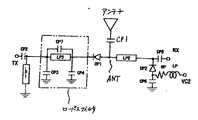
図1は、本発明の1実施例で、スイッチ素子としてダイオードを使用したシングルバンド携帯電話に用いる高周波スイッチモジュールの回路を示す。
スイッチ回路の機能は、送信回路と受信回路を電気的に高速に切替分離してアンテナ端子を介してアンテナと接続することである。このスイッチ回路は、2つのダイオードDP1、DP2と、2つの伝送線路LP1、LP2からなり、ダイオードDP1はアンテナ端子ANT側にアノードが接続され、送信TX側にカソードが接続され、そのカソード側にアースに接続される伝送線路LP1が接続されている。
通常アンテナは、高周波スイッチモジュールの外にロット状、ワイヤ状のものが取り付けられ、高周波スイッチモジュールのアンテナ端子ANTに接続されるが、今後モジュール化の要請が更に強まると、平面アンテナを更に複合化して取り込んだ高周波スイッチモジュールも考えられる。本発明は、実施例としてはアンテナを外部取り付けしたものを例示するが、アンテナを含んだ複合モジュールにも適用できる。
そして、アンテナ側と受信RX間に伝送線路LP2が接続され、その受信RX側にカソードが接続されたダイオードDP2が接続され、そのダイオードDP2のアノードには、アースとの間にコンデンサCP6が接続され、その間にインダクタが接続され、コントロール回路VC2に接続される。コントロール回路VC2に電圧(例えば+3V、+2.6V)を印加すると、ダイオードDP2,DP1がONして送信回路TXとアンテナ端子ANTが接続される。コントロール回路に電圧を印加しない場合には、アンテナ端子ANTと受信系RXが接続されている。このようにして、1つのアンテナを送受信系の両方が共用できる。コントロール回路の端子VC2に接続されたインダクタLPは、電源側を見たインピーダンスを大きくすることにより、電源側のインピーダンスが負荷変動などにより変動しても影響を阻止する機能がある。
この実施例では、スイッチ回路にダイオードを用いたので、高周波における耐電力に優れ、低損失という効果がある。
この実施例では更に、送信TX回路側にローパスフィルタ回路を挿入する。即ち、伝送線路LP3と、コンデンサCP3、CP4、CP7から構成され、スイッチ回路SWのダイオードDP1と伝送線路LP1の間に挿入されている。ローパスフィルタを入れると、アンプ(増幅器)等から発生する高調波を抑制できる。
図1のシングルバンドの高周波スイッチモジュールを実装した一実施例の斜視図を図2に示す。DPはダイオードDP1とダイオードDP2をパッケージングした電子部品である。側面電極は一切使用せず、積層体の層間の電気的接続は、全てスルーホールで行った。
図3では、底面の外部電極を、図2の場合にはパターン印刷法によったが、この場合には半田ボールBALLによるBGA(ボール・グリッドアレイ)で行った。BGA以外のグリッドアレイも使える。
【0008】
図4にスイッチ素子としてダイオードを使用したデュアルバンド携帯電話に使用する高周波スイッチモジュールの1実施例を示す。
この実施例は、通過帯域の異なる第1の送受信系(EGSM900)と第2の送受信系(GSM1800)を扱う高周波スイッチモジュールであり、第1の送受信系(EGSM900)の送信信号と受信信号を切り換える第1のスイッチ回路、第1のスイッチ回路の送信ラインに接続される第1のローパスフィルタ回路、第2の送受信系(GSM1800)の送信信号と受信信号を切り換える第2のスイッチ回路、第2のスイッチ回路の送信ラインに接続される第2のローパスフィルタ回路、第1の送受信系と第2の送受信系を分波する分波回路から構成されている。
アンテナ端子ANTに接続される分波回路部分は、2つのノッチ回路が主回路となっている。つまり、伝送線路LF1とコンデンサCF1で一つのノッチ回路を構成し、伝送線路LF2とコンデンサCF2でもう一つのノッチ回路を構成している。
そして、一つのノッチ回路には、アースに接続されるコンデンサCF3が接続されている。このコンデンサCF3は、分波特性のローパスフィルタ特性を向上させる目的で接続されている。また、もう一つのノッチ回路には、アースに接続される伝送線路LF3と、コンデンサCF4を直列に接続している。この伝送線路LF3とコンデンサCF4は、分波特性のハイパスフィルタ特性を向上させる目的で接続されている。
この分波回路は、ノッチ回路以外、例えばバンドパス回路、ローパス回路、ハイパス回路などを用いてもよく、これらを適宜組み合わせて構成することも出来る。
次に、第1のスイッチ回路について説明する。第1のスイッチ回路は、図4上側のスイッチ回路であり、EGSM900系の送信TXと受信RXを切り換えるものである。このスイッチ回路SWは、2つのダイオードDG1、DG2と、2つの伝送線路LG1、LG2からなり、ダイオードDG1はアンテナ端子ANT側にアノードが接続され、送信TX側にカソードが接続され、そのカソード側にアースに接続される伝送線路LG1が接続されている。そして、アンテナ側と受信RX間に伝送線路LG2が接続され、その受信側にカソードが接続されたダイオードDG2が接続され、そのダイオードDG2のアノードには、アースとの間にコンデンサCG6が接続され、その間にインダクタLGが接続され、コントロール回路VC1に接続される。
そして、送信TX回路側に挿入されるローパスフィルタ回路は、伝送線路LG3と、コンデンサCG3、CG4、CG7から構成され、スイッチ回路SWのダイオードDG1と伝送線路LG1の間に挿入されている。
次に、第2のスイッチ回路について説明する。第2のスイッチ回路は、図4下側のスイッチ回路であり、GSM1800系の送信TXと受信RXを切り換えるものである。このスイッチ回路SWは、2つのダイオードDP1、DP2と、2つの伝送線路LP1、LP2からなり、ダイオードDP1はアンテナ端子ANT側にアノードが接続され、送信TX側にカソードが接続され、そのカソード側にアースに接続される伝送線路LP1が接続されている。そして、アンテナ側と受信RX間に伝送線路LP2が接続され、その受信RX側にカソードが接続されたダイオードDP2が接続され、そのダイオードDP2のアノードには、アースとの間にコンデンサCP6が接続され、その間にインダクタが接続され、コントロール回路VC2に接続される。
コントロール回路の動作を説明する。EGSM900系の送信を有効とする場合には、電圧端子VC1に所定の電圧を印加する。同様に、電圧端子VC2に所定の電圧を印加するとGSM1800系の送信が有効となる。受信時には、どちらの電圧端子VC1,VC2にも電圧を印加しない。
そして、送信TX回路側に挿入されるローパスフィルタ回路は、伝送線路LP3と、コンデンサCP3、CP4、CP7から構成され、スイッチ回路SWのダイオードDP1と伝送線路LP1の間に挿入されている。
【0009】
図4に示す実施例には、伝送線路LG2,LP2と受信RX(RX/EGSM900,RX/GSM1800)の間に、SG、SPで示される弾性表面波素子(SAW)を用いたバンドパスフィルタを接続してある。SAWフィルタを用いることにより、小型化できるし、電気的にもQ(共振回路の先鋭度)の高いフィルタとなり、小型かつ受信信号の選択度が良くなるという効果がある。
図4において、コンデンサCGPの機能は、高周波的に伝送線路LG1とLP1の接続点N1とアースとの間のインピーダンスを低くするものである。
図4の抵抗Rの機能は、ダイオードに流す電流値を制御する為である。この実施例では、EGSM900系とGSM1800系の各々のコントロール回路VC1、VC2に共通になるように構成したので部品点数を低減できる。
なお、図4において伝送線路とSAWフィルタの間にDC(直流)カットのコンデンサは不要である。 SAWフィルタが、その構造上DC(直流)を遮断できるからである。
以上、本発明をシングルバンド、デュアルバンド高周波スイッチモジュールについて説明したが、トリプルバンド以上のマルチバンドに適用できる。
【0010】
図5に、SG、SPで示される弾性表面波素子(SAW)を用いたバンドパスフィルタを用いた高周波スイッチモジュールの斜視図を示す。図3では、側面電極を使わずにスルーホールだけで回路を構成して、高周波スイッチモジュールの底部に電極を集中した。
SAWフィルタ(SG,SP)、PINダイオード(DG1,DG2,DP1,DP2)、コンデンサ(CG1,CGP)、抵抗R以外は、全て積層体MLに印刷回路として形成した。配置の概略は、図5の手前に2個のSAWフィルタSP、SG、図5の左方に分波器を配置し、グランドパターンが形成された誘電体層を介して、その下にスイッチ回路とローパスフィルタ、更にグランドパターンが形成された誘電体層をサンドイッチして、コンデンサのパターンが印刷された誘電体層、そして、一番下にグランドパターンを配置した。図5に示す実装では、積層体ML1、ML2に段差を設けてSAWフィルタ(SG,SP)を配置したので、低背化が実現でき、更に小型化が可能となった。積層体ML1、ML2は一体構造である。
【0011】
本発明は、図5に示すように高周波スイッチモジュールを、積層構造及びその積層体上にチップ部品を配置することにより、小型に構成できる。
複数の送受信系の共通端子であるアンテナ端子ANT、各送受信系のそれぞれの送信系端子TX、受信系端子RXは高周波信号用の端子であり、これを高周波端子と呼ぶ。この高周波端子は、図6に例示するように積層体の裏面に形成され、しかもこの高周波端子同士が隣り合わないように配置した。各高周波端子の記号は、図4の等価回路と対応している。EGSM900とGSM1800の共通の端子としてアンテナ端子ANTがある。これは外部に接続されるアンテナへの入出力端子となる。なお、この実施例では、アンテナは外部取付の例を示したが、今後ますます複合機能化が進展してモジュール化が進むと、積層体に平面アンテナを複合化することも考えられる。本発明は、この場合にも適用できる。
図6で、TX、RXは、 EGSM900とGSM1800共に、前者が送信端子、後者が受信端子である。VC1,VC2は、コントロール端子で、外部電源からコントロール回路を経てスイッチ回路の切替を行い、送信/受信の切替を制御する端子である。
この高周波端子間には、グランド端子GND又はスイッチ回路制御端子(VC1,VC2)が配置される。また、この高周波端子間には、少なくとも1つのグランド端子GNDが配置されることが好ましい。このように、高周波端子間を隣り合わないようにすること、又高周波端子間にグランド端子をサンドイッチして配置することにより、高周波端子間の干渉を抑え、又低損失化を計ることができる。
【0012】
送信系端子と受信系端子とは、送信系端子同士、又受信系端子同士が隣り合わない程度に近接して配置されることが好ましい。また、積層体の中心線に対し、別々の領域に、それぞれ送信系端子、受信系端子を配置することが好ましい。また、この送信系端子、受信系端子は線対称に配置されていることが好ましい。このように構成することにより、高周波スイッチモジュールが実装される複数の送受信系を扱う装置において、送信系回路、受信系回路と接続し易い。
【0013】
共通端子と、それぞれの送受信系の送信端子、受信端子とは、積層体を実装面に垂直な面で2分した場合、別領域に形成することが好ましい。この高周波スイッチモジュールは、アンテナと送受信回路の間に配置されるので、この端子配置により、アンテナと高周波スイッチモジュール、及び送受信回路と高周波スイッチモジュールを最短の線路で接続することができ、余分な損失を防止できる。
【0014】
本発明では、積層体上に配置されたチップ部品を囲むように金属ケースを配置することが好ましい。シールド効果だけでなく、高周波スイッチモジュールのユーザがチップマウンタで半田付けする際に、金属ケースだと真空吸引し易いからである。シールド効果が要求されず、単にチップマウンタの供給用としての平面形成の為だけなら、高周波スイッチモジュールをリフロー半田時の熱に耐えられる耐熱性の樹脂でモールドしたり、その上を金属コーティングしても良い。
金属ケースは、積層体の上面または下面に半田付けで固定することができる。
また、この金属ケースにより、マウンタ装置により、本発明の高周波スイッチモジュールを実装することができる。
また、受信系のバンドパスフィルタとしてSAW(弾性表面波)フィルタを用いる場合、既にパッケージングされ市販されるSAWフィルタを用いても良いが、ベアチップ、フリップチップのSAWフィルタを用いて、高周波スイッチモジュール全体をパッケージングすれば、なお小型化、高性能化できる。
【0015】
この積層体の内部構造について説明する。図7と図8に各層の印刷パターン図を示す。この実施例は、1層の厚みが50μm(一体焼成後の寸法)の誘電体シートに各層の電極を印刷してスルーホールで接続した例である。図7,図8でスルーホールは、×印を付けたランドである。×部に孔が開いてスルーホールを形成している。
誘電体としては、例えばアルミナ系ガラスセラミック低温焼結材料が挙げられる。
図7は積層体の一番上の層(1)から50μmの層厚毎に、第8層(8)迄を、図8は更にその下の層である第9層(9)から第18層(18)迄を示す。パターンに付したDG1、CG1,DG2等の記号は、図4の等価回路と対応する。
【0016】
この積層体は、低温焼成が可能なセラミック誘電体材料からなるグリーンシートを用意し、そのグリーンシート上にAg、Pd,Cu等の導電ペーストを印刷して、所望の電極パターンを形成し、それを適宜積層し、一体焼成させて構成される。なお、シートの厚さは大体80〜250μmの範囲で、使用用途によりドクターブレード法などで制御される。所定の内部電極パターンを多数形成した大きなシートを積層し、1つ1つのチップサイズに切断した後、焼成、端子電極形成をし、誘電体積層素体を作製する。端子電極は、通常、Ag−Ni−半田の3層構造をしており、 Ni層により半田耐熱性、半田層により半田濡れ性を十分得られるようにしている。この誘電体積層素体上にメタルマスクを使用した半田印刷を行い、その後PINダイオードや、容量値が大きく積層素体内に形成出来なかったチップコンデンサ、場合によっては弾性表面波フィルタなどを搭載し、リフロー半田付する。
以下、焼成後の各層の構成を、最下層から順に説明する。
まず、最下層の第18層(図8(18))上には、グランド電極GNDがほぼ全面(GND電極については、分かり易い様にパターンを塗りつぶした)に形成されている。これにより安定したアースが確保できる。特に、この実施例では複数のスルーホール(図8(18)の場合、左右各々6個のスルーホール)で裏面に連通し、図4に示す幅広で細長いGNDとして外部回路との接続に使え、安定したアース効果が得られる。
第17層(図8(17))には、コンデンサ用電極(CG6,CGL,CP6,CPL)が形成される。これらのコンデンサは、スイッチ回路のダイオードの開閉を制御するコントロール回路に用いる。
第16層(図8(16))にも、GND電極がほぼ全面に形成されている。
第15層(図8(15))の一点鎖線を境に、手前側にGSM1800系、反対側にEGSM900系を配置した。これにより接続の最短化を計り、電気的特性の向上が図れる。
第15層(図8(15))から第11層(図8(11))にかけて、層の右半分にコントロール回路のインダクタンスLG、LPを多層に亘ってコイル構成した。第15層(図8(15))の左半分は、ローパスフィルタのコンデンサパターン(CG3,CG4,CP3,CP4)を配置した。
第14層(図8(14))には、右半分に前述のインダクタンスLG、LPのパターンの一部、左半分にローパスフィルタのコンデンサCG7,CP7を配置した。
第13層(図8(13))には、右半分に前述のインダクタンスLG、LPのパターンの一部、左側にスイッチ回路の伝送線路、LG1,LG2、LP2,LP3を配置した。スイッチ回路とローパスフィルタとを同一面上に配置したので、両者のマッチングが更に向上した。
第12層(図8(12))には、右半分に前述のインダクタンスLG、LPのパターンの一部、左側に前述のスイッチ回路の伝送線路、LG1,LG2、LP2,LP3のパターンの一部と、同じくスイッチ回路の伝送線路LG1,LP1を配置した。
第11層(図8(11))には、右半分に前述のインダクタンスLG、LPのパターンの一部、左側に前述のスイッチ回路の伝送線路、LG1,LG2、LP2,LP3のパターンの一部と、同じくスイッチ回路の伝送線路LG1,LP1のパターンの一部を配置した。
第10層(図8(10))にはEGSM900系のスイッチ回路の伝送線路LG2,LG3のパターンの一部を配置した。
第9層(図8(9))には、中央に示す縦線から右側に受信系のローパスフィルタであるSAWフィルタSG,SP用のパターンを配置した。中央に示す縦線の左側に分波回路のパターンを配置した。
【0017】
図7に示す各層は、図8に示す各層と違い、右方を欠いた形状である。図7の破線は、それ以下の図8の各層に対応する部分を示す。このような形状の組合せにより、図5に示すような段差付きの積層体ML1,ML2が得られ、段差部にSAWフィルタSG、SPを搭載したコンパクトな高周波スイッチモジュールが得られた。積層体ML1は図7,積層体ML2は図8に対応する。
この段差の形成方法の一例を説明する。まず、同一寸法のグリーンシートに図7,図8に示す各電極パターンを印刷する。図7のパターンの場合には、左部のみの印刷で、右部には印刷パターンはない。次に各グリーンシートを積層してゆくのであるが、第18層(図8(18))から積層して第9層(図8(9))を積層した後、グリーンシートの厚み80μm程度に比べて十分に薄く(20μm程度)且つグリーンシートから剥離可能なPET(ポリエチレンテレフタレート)シート等(剥離シートと呼ぶ)を図7の破線で示す部分に挿入し、更に第8層(図7(8))から第1層(図7(1))まで積層して積層体を完成する。その後、図7の縦線部から超硬刃で切り込みを剥離シートの上まで入れ、剥離シートごと、その上のグリーンシート積層体を除去すると、図5に示す段差部が容易に形成できる。
以下、積層体ML1に対応する各層の配置を、図7を用いて説明を続ける。
第8層と第7層(図7(8)と(7))には分波回路のコンデンサCF1,CF2,CF4のパターンを印刷する。
第6層(図7(6))はダミー層である。ダミー層とは上下の層(第5層、第7層)に形成された電極パターンを電気的に接続するスルーホールを設け、他の電極パターンが全く印刷されてないものをいう。積層体においてアンテナ端子ANTと伝送線路LF1、LF2、LF3との距離を隔てる為に設けた。
なお、ダミー層ではなくて、アンテナ端子ANTと伝送線路LF1、LF2、LF3がパターン印刷される層の層厚を変えても良い。ダミー層を用いる場合には、全部の層を1つの例えば50μmのシートで形成でき、生産性が向上する効果がある。
第5層と第4層(図7(5)と(4))は、分波回路のフィルタを構成する伝送線路LF1〜LF3を配置した。第3層(図7(3))は、分波回路のフィルタを構成する伝送線路LF1、LF2を配置した。これにより、グランドパターンGND(図8(16)、(18))から最も離して配置でき、両者間の間隔を最大にしたので、インダクタンスを十分大きく取れる。
第1層には積層体ML1の上に取り付ける部品であるダイオードDG1,DG2,DP1,DP2、コンデンサCG1,CGP、抵抗Rのパターンを設けた。
なお、第2層(図7(2))はそれら搭載部品を積層体内の他のパターンと接続するためのパターンを示す。
【0018】
以上、受信系のバンドパスフィルタとしてSAWフイルタを用い、且つ積層体に段差を設けて小型化した高周波スイッチモジュールの一実施例を示したが、本発明は段差を設けた積層体に限定されず、積層体にキャビティ(凹部)を設けてSAWフイルタを搭載してもよい。
【0019】
以上、本発明により、シングルバンドにみならず、デュアルバンド以上のマルチバンド携帯電話においても、各信号を分離・合成する分波器1個、送信信号と受信信号を切り替えるアンテナスイッチと、高周波除去用のローパスフィルタを各1個づつ、最小限の素子を誘電体の積層体に内蔵し、その素体上にスイッチ素子を搭載した超小型の高周波スイッチモジュールを実現した。
【0020】
【発明の効果】
本発明によると、超小型化に対応できる高周波スイッチモジュールを提供することができる。本発明によれば、この高周波スイッチモジュールを、好ましくは積層構造を用いることにより、小型に、しかもワンチップに構成できる。これにより、デュアルバンド携帯電話などにおいて、機器の超小型化に有効となる。
【図面の簡単な説明】
【図1】本発明に係る一実施例の等価回路図である。
【図2】本発明に係る一実施例の斜視図である。
【図3】本発明に係る別の実施例の斜視図である。
【図4】本発明に係る別の実施例の等価回路図である。
【図5】本発明に係る別の実施例の斜視図である。
【図6】本発明に係る高周波スイッチモジュールの底面の電極配置を示す図である。
【図7】図4に示す等価回路の積層体の各層のパターンを示す図である。
【図8】積層体の各層のパターンの続きを示す図である。
【図9】従来の高周波スイッチモジュールの斜視図である。
【符号の説明】
LG1,LP1 伝送線路
LF2,LF3 伝送線路
LP2,LP3 伝送線路
TX 送信系端子
RX 受信系端子
ANT アンテナ端子
SG,SP 弾性表面波フィルタ[0001]
BACKGROUND OF THE INVENTION
The present invention relates to a high-frequency composite component used in a high-frequency band such as a quasi-microwave band, and relates to a high-frequency switch module that handles a transmission / reception system with at least one antenna.
[0002]
[Prior art]
In recent years, the spread of mobile phones has been remarkable, and the functions and services of mobile phones have been improved. Initially, it started with a single-band mobile phone sharing one antenna for one transmission / reception system. For this purpose, a high-frequency switch using a laminated body has also been developed (see, for example, Japanese Patent Laid-Open Nos. 6-197040 and 9-36603).
Since then, with the rapid increase in the number of subscribers, dual-band mobile phones and the like have appeared on the market. This dual-band mobile phone handles two transmission / reception systems, whereas an ordinary mobile phone handles only one transmission / reception system. Thereby, the user can select and use a convenient transmission / reception system.
For example, in a dual-band mobile phone, the GSM1800 system (transmission TX. 1710 to 1785 MHz, reception RX. 1805 to 1880 MHz) and the EGSM 900 system (transmission TX. 880 to 915 MHz, reception RX. 925 to 960 MHz) as the second transmission / reception system It corresponds to two systems.
In such a cellular phone, a signal module corresponding to each frequency, and a switch module configured by using a branching circuit and a switch circuit as a switch for switching a plurality of frequencies are used (for example, JP-A-9-36604). No., JP 11-55002 A).
[0003]
[Problems to be solved by the invention]
As shown in FIG. 9, the conventional high-frequency switch module is provided with an external connection terminal EXT on the side surface. This is because when the high frequency switch module is soldered to the printed circuit board, a fillet is formed and the solder strength is increased. The external connection terminals include a transmission terminal TX, a reception terminal RX, a control terminal VC of the switch circuit, a ground terminal GND, and the like.
However, when the external connection terminal EXT is provided on the side surface portion, there is a possibility that a short circuit occurs due to a solder bridge (bridge) with an electronic component DP such as a PIN diode constituting an antenna switching switch circuit mounted on the multilayer ML. This is because the distance between them is too close.
This has become prominent in the trend toward miniaturization of high-frequency switch modules. The trend toward miniaturization often leads to not only a short circuit between the external connection terminal EXT and the electronic component DP but also a short circuit between the external connection terminals EXT. This is a problem that significantly limits the degree of freedom of design in a high-frequency switch module in which a trend toward downsizing is inevitable.
Accordingly, the present invention has been made to solve such problems, and it is an object of the present invention to provide a high-frequency switch module that is ultra-small, has no fear of a solder bridge, and has excellent electrical characteristics. is there.
[0004]
[Means for Solving the Problems]
The gist of the present invention is as follows.
The present invention is a high frequency switch module comprising a switch element mounted on a laminate and an electrode pattern formed on a dielectric layer of the laminate, wherein a side electrode is formed on a side surface of the laminate. There is no electrical connection between the electrode patterns of each layer, and a plurality of high-frequency terminals, switch circuit control terminals, ground terminals, and ground terminals and inner layer electrode patterns formed on the peripheral edge of the bottom surface are all formed through holes. On the lower layer side of the body, a ground electrode is formed on almost the entire surface including between the through-holes connected to the high-frequency terminal, and the first through-hole connected to the high-frequency terminal is formed on the dielectric layer on which the ground electrode is formed. A hole and a second through hole connected to the switch circuit control terminal are formed side by side, and an outer edge of the ground electrode is a first through hole and a second through hole. With extends between a high-frequency switch module, characterized by being formed with a distance inwardly from the outer circumferential portion of the laminate.
In the present invention, a diode or a transistor is used as the switch element, and a plurality of surface acoustic wave elements through which received signals of different transmission / reception systems pass are mounted on the mounting surface of the switch element of the laminate, and the surface acoustic wave element is It is preferable that they are arranged side by side on one side of the mounting surface, and each is connected to the ground electrode via a via hole.
It is also preferable to form an external connection terminal with a solder ball at the bottom of the laminate.
[0005]
The present inventor anticipates the inevitable trend toward miniaturization of high-frequency switch modules, and it is a future design concept that a high-frequency switch module circuit is configured only by through holes (also called via holes or via holes) without using side electrodes. I foreseeed to become.
Furthermore, a design concept for converting a conventional pattern electrode into a BGA (ball grid array) was foreseen. In pattern printing, the width of the pattern that can be printed is considered to be the limit that can be produced with high accuracy without blurring, and it is predicted that if the pitch becomes smaller than that, it will become a grid array, especially a BGA (ball grid array). .
[0006]
DETAILED DESCRIPTION OF THE INVENTION
First, a high-frequency switch module according to the present invention will be described with reference to the drawings. 1 shows a single band, and FIG. 2 shows an equivalent circuit when applied to a dual band.
[0007]
FIG. 1 shows a circuit of a high-frequency switch module used in a single-band mobile phone using a diode as a switch element according to an embodiment of the present invention.
The function of the switch circuit is to electrically switch and separate the transmission circuit and the reception circuit at high speed and to connect to the antenna via the antenna terminal. This switch circuit includes two diodes DP1 and DP2 and two transmission lines LP1 and LP2. The diode DP1 has an anode connected to the antenna terminal ANT side, a cathode connected to the transmission TX side, and a ground connected to the cathode side. Is connected to the transmission line LP1.
Usually, a lot or wire is attached outside the high-frequency switch module and connected to the antenna terminal ANT of the high-frequency switch module. However, if the demand for modularization becomes stronger in the future, the planar antenna will be further combined. A high-frequency switch module incorporated in The present invention exemplifies an externally attached antenna as an embodiment, but can also be applied to a composite module including an antenna.
A transmission line LP2 is connected between the antenna side and the reception RX, a diode DP2 having a cathode connected to the reception RX side is connected, and a capacitor CP6 is connected between the anode of the diode DP2 and the ground. In the meantime, an inductor is connected to the control circuit VC2. When a voltage (for example, + 3V, + 2.6V) is applied to the control circuit VC2, the diodes DP2 and DP1 are turned on to connect the transmission circuit TX and the antenna terminal ANT. When no voltage is applied to the control circuit, the antenna terminal ANT and the receiving system RX are connected. In this way, both antennas can share one antenna. The inductor LP connected to the terminal VC2 of the control circuit has a function of preventing the influence even if the impedance on the power supply side fluctuates due to a load fluctuation or the like by increasing the impedance seen from the power supply side.
In this embodiment, since the diode is used for the switch circuit, it has excellent power resistance at high frequencies and low loss.
In this embodiment, a low-pass filter circuit is further inserted on the transmission TX circuit side. That is, the transmission line LP3 and the capacitors CP3, CP4, and CP7 are inserted between the diode DP1 of the switch circuit SW and the transmission line LP1. When a low-pass filter is inserted, harmonics generated from an amplifier (amplifier) or the like can be suppressed.
FIG. 2 is a perspective view of an embodiment in which the single-band high-frequency switch module of FIG. 1 is mounted. DP is an electronic component in which the diode DP1 and the diode DP2 are packaged. Side electrodes were not used at all, and all the electrical connections between the layers of the laminate were made through holes.
In FIG. 3, the external electrodes on the bottom surface are formed by a pattern printing method in the case of FIG. 2, but in this case, BGA (ball grid array) using solder balls BALL is performed. Grid arrays other than BGA can also be used.
[0008]
FIG. 4 shows an embodiment of a high-frequency switch module used in a dual-band mobile phone using a diode as a switch element.
This embodiment is a high-frequency switch module that handles a first transmission / reception system (EGSM900) and a second transmission / reception system (GSM1800) having different passbands, and switches between a transmission signal and a reception signal of the first transmission / reception system (EGSM900). A first switch circuit; a first low-pass filter circuit connected to a transmission line of the first switch circuit; a second switch circuit that switches between a transmission signal and a reception signal of the second transmission / reception system (GSM1800); A second low-pass filter circuit connected to the transmission line of the switch circuit, and a demultiplexing circuit for demultiplexing the first transmission / reception system and the second transmission / reception system.
The branching circuit portion connected to the antenna terminal ANT has two notch circuits as main circuits. That is, the transmission line LF1 and the capacitor CF1 constitute one notch circuit, and the transmission line LF2 and the capacitor CF2 constitute another notch circuit.
A capacitor CF3 connected to the ground is connected to one notch circuit. The capacitor CF3 is connected for the purpose of improving the low-pass filter characteristic of the demultiplexing characteristic. Further, the transmission line LF3 connected to the ground and the capacitor CF4 are connected in series to the other notch circuit. The transmission line LF3 and the capacitor CF4 are connected for the purpose of improving the high-pass filter characteristic of the demultiplexing characteristic.
As the branching circuit, for example, a bandpass circuit, a lowpass circuit, a highpass circuit, or the like other than the notch circuit may be used, and these may be combined as appropriate.
Next, the first switch circuit will be described. The first switch circuit is a switch circuit on the upper side of FIG. 4 and switches between EGSM900 transmission TX and reception RX. The switch circuit SW includes two diodes DG1 and DG2 and two transmission lines LG1 and LG2. The diode DG1 has an anode connected to the antenna terminal ANT side, a cathode connected to the transmission TX side, and a cathode side thereof. A transmission line LG1 connected to the ground is connected. A transmission line LG2 is connected between the antenna side and the reception RX, a diode DG2 having a cathode connected to the reception side is connected, and a capacitor CG6 is connected between the anode of the diode DG2 and the ground, In the meantime, the inductor LG is connected to the control circuit VC1.
The low-pass filter circuit inserted on the transmission TX circuit side includes a transmission line LG3 and capacitors CG3, CG4, and CG7, and is inserted between the diode DG1 of the switch circuit SW and the transmission line LG1.
Next, the second switch circuit will be described. The second switch circuit is a switch circuit on the lower side of FIG. 4 and switches between GSM1800 transmission TX and reception RX. The switch circuit SW includes two diodes DP1 and DP2 and two transmission lines LP1 and LP2. The diode DP1 has an anode connected to the antenna terminal ANT side, a cathode connected to the transmission TX side, and a cathode side thereof. A transmission line LP1 connected to the ground is connected. A transmission line LP2 is connected between the antenna side and the reception RX, a diode DP2 having a cathode connected to the reception RX side is connected, and a capacitor CP6 is connected between the anode of the diode DP2 and the ground. In the meantime, an inductor is connected to the control circuit VC2.
The operation of the control circuit will be described. In order to validate the transmission of the EGSM900 system, a predetermined voltage is applied to the voltage terminal VC1. Similarly, when a predetermined voltage is applied to the voltage terminal VC2, GSM1800 transmission becomes effective. At the time of reception, no voltage is applied to either voltage terminal VC1, VC2.
The low-pass filter circuit inserted on the transmission TX circuit side includes a transmission line LP3 and capacitors CP3, CP4, and CP7, and is inserted between the diode DP1 of the switch circuit SW and the transmission line LP1.
[0009]
In the embodiment shown in FIG. 4, a band-pass filter using surface acoustic wave elements (SAW) indicated by SG and SP is provided between the transmission lines LG2 and LP2 and the receiving RX (RX / EGSM900, RX / GSM1800). Connected. By using the SAW filter, it is possible to reduce the size, and the filter is electrically high in Q (sharpness of the resonance circuit), and has an effect of being small and improving the selectivity of the received signal.
In FIG. 4, the function of the capacitor CGP is to reduce the impedance between the connection point N1 of the transmission lines LG1 and LP1 and the ground in a high frequency manner.
The function of the resistor R in FIG. 4 is to control the value of current flowing through the diode. In this embodiment, since it is configured to be common to the control circuits VC1 and VC2 of the EGSM900 system and the GSM1800 system, the number of parts can be reduced.
In FIG. 4, a DC (direct current) cut capacitor is not required between the transmission line and the SAW filter. This is because the SAW filter can block DC (direct current) due to its structure.
Although the present invention has been described with respect to the single-band and dual-band high-frequency switch modules, the present invention can be applied to multibands of triple bands or more.
[0010]
FIG. 5 shows a perspective view of a high-frequency switch module using a band-pass filter using surface acoustic wave elements (SAW) indicated by SG and SP. In FIG. 3, the circuit is configured with only through holes without using the side electrodes, and the electrodes are concentrated on the bottom of the high-frequency switch module.
Except for the SAW filter (SG, SP), PIN diode (DG1, DG2, DP1, DP2), capacitor (CG1, CGP), and resistor R, all were formed as a printed circuit in the multilayer ML. The outline of the arrangement is that two SAW filters SP and SG are arranged in front of FIG. 5, a duplexer is arranged on the left side of FIG. 5, and a switch circuit is provided below the dielectric layer on which a ground pattern is formed. And a low-pass filter, and a dielectric layer on which a ground pattern is formed are sandwiched, a dielectric layer on which a capacitor pattern is printed, and a ground pattern at the bottom. In the mounting shown in FIG. 5, since the SAW filters (SG, SP) are arranged by providing steps on the stacked bodies ML1 and ML2, it is possible to reduce the height and further reduce the size. The stacked bodies ML1 and ML2 have an integral structure.
[0011]
In the present invention, as shown in FIG. 5, the high-frequency switch module can be configured in a small size by arranging a chip structure on the laminated structure and the laminated body.
An antenna terminal ANT, which is a common terminal for a plurality of transmission / reception systems, a transmission system terminal TX for each transmission / reception system, and a reception system terminal RX are terminals for high-frequency signals, which are called high-frequency terminals. The high frequency terminals are formed on the back surface of the laminate as illustrated in FIG. 6 and are arranged so that the high frequency terminals are not adjacent to each other. The symbol of each high frequency terminal corresponds to the equivalent circuit of FIG. There is an antenna terminal ANT as a common terminal of the EGSM900 and GSM1800. This is an input / output terminal for an externally connected antenna. In this embodiment, an example in which the antenna is externally mounted has been shown. However, as the multi-functionalization progresses and modularization proceeds in the future, a planar antenna may be combined with the laminate. The present invention can also be applied to this case.
In FIG. 6, for TX and RX, the former is a transmission terminal and the latter is a reception terminal in both EGSM900 and GSM1800. VC1 and VC2 are control terminals that switch the switch circuit from the external power source through the control circuit and control the switching of transmission / reception.
Between the high-frequency terminals, a ground terminal GND or a switch circuit control terminal (VC1, VC2) is disposed. Further, it is preferable that at least one ground terminal GND is disposed between the high frequency terminals. In this way, by preventing the high frequency terminals from being adjacent to each other and arranging the ground terminals sandwiched between the high frequency terminals, interference between the high frequency terminals can be suppressed and loss can be reduced.
[0012]
The transmission system terminal and the reception system terminal are preferably arranged close to each other so that the transmission system terminals and the reception system terminals are not adjacent to each other. Moreover, it is preferable to arrange | position a transmission type | system | group terminal and a receiving system terminal in a respectively separate area | region with respect to the centerline of a laminated body. Further, it is preferable that the transmission system terminal and the reception system terminal are arranged in line symmetry. With this configuration, it is easy to connect to a transmission system circuit and a reception system circuit in an apparatus that handles a plurality of transmission / reception systems on which a high frequency switch module is mounted.
[0013]
The common terminal and the transmission terminal and the reception terminal of each transmission / reception system are preferably formed in different regions when the laminate is divided into two parts by a plane perpendicular to the mounting surface. Since this high-frequency switch module is arranged between the antenna and the transmission / reception circuit, this terminal arrangement allows the antenna and the high-frequency switch module, and the transmission / reception circuit and the high-frequency switch module to be connected with the shortest line, resulting in an extra loss. Can be prevented.
[0014]
In the present invention, it is preferable to dispose a metal case so as to surround the chip component disposed on the laminate. This is because not only the shielding effect but also the user of the high-frequency switch module can easily vacuum the metal case when soldering with a chip mounter. If the shielding effect is not required, and it is only for forming a flat surface for supplying a chip mounter, the high-frequency switch module is molded with a heat-resistant resin that can withstand the heat during reflow soldering, or a metal coating is applied on it. Also good.
The metal case can be fixed to the upper surface or the lower surface of the laminate by soldering.
Moreover, the high frequency switch module of this invention can be mounted with a mounter apparatus by this metal case.
In addition, when a SAW (surface acoustic wave) filter is used as a reception band-pass filter, a commercially available SAW filter may be used, but a bare chip or flip chip SAW filter may be used. If the whole is packaged, the size and performance can be improved.
[0015]
The internal structure of this laminate will be described. 7 and 8 show print pattern diagrams of each layer. In this example, electrodes of each layer are printed on a dielectric sheet having a thickness of 50 μm (size after integral firing) and connected by through holes. In FIG. 7 and FIG. 8, the through hole is a land marked with a cross. A through hole is formed by opening a hole in the x portion.
Examples of the dielectric include alumina-based glass ceramic low-temperature sintered material.
FIG. 7 shows the layers from the top layer (1) to the eighth layer (8) every 50 μm, and FIG. 8 shows the ninth layer (9) to the eighteenth layer. Up to layer (18) is shown. Symbols such as DG1, CG1, and DG2 attached to the pattern correspond to the equivalent circuit of FIG.
[0016]
For this laminate, a green sheet made of a ceramic dielectric material that can be fired at a low temperature is prepared, and a conductive paste such as Ag, Pd, or Cu is printed on the green sheet to form a desired electrode pattern. Are appropriately laminated and integrally fired. The sheet thickness is generally in the range of 80 to 250 μm, and is controlled by the doctor blade method or the like depending on the intended use. After laminating large sheets on which a large number of predetermined internal electrode patterns are formed and cutting them into individual chip sizes, firing and terminal electrode formation are performed to produce a dielectric multilayer body. The terminal electrode usually has a three-layer structure of Ag—Ni—solder, and the solder resistance of the solder is obtained by the Ni layer and the solder wettability is sufficiently obtained by the solder layer. Solder printing using a metal mask is performed on this dielectric multilayer body, and then a PIN diode, a chip capacitor with a large capacitance value that could not be formed in the multilayer body, and in some cases a surface acoustic wave filter, etc. Reflow soldering.
Hereinafter, the structure of each layer after baking is demonstrated in an order from the lowest layer.
First, on the lowermost 18th layer (FIG. 8 (18)), the ground electrode GND is formed on almost the entire surface (the GND electrode is filled with a pattern for easy understanding). As a result, a stable ground can be secured. In particular, in this embodiment, a plurality of through holes (in the case of FIG. 8 (18), six through holes on the left and right sides) communicate with the back surface, and can be used for connection to an external circuit as a wide and narrow GND shown in FIG. A stable grounding effect can be obtained.
Capacitor electrodes (CG6, CGL, CP6, CPL) are formed on the seventeenth layer (FIG. 8 (17)). These capacitors are used in a control circuit that controls the opening and closing of the diode of the switch circuit.
In the 16th layer (FIG. 8 (16)), the GND electrode is formed on almost the entire surface.
A GSM1800 system is arranged on the front side and an EGSM900 system is arranged on the opposite side, with a dot-and-dash line in the 15th layer (FIG. 8 (15)) as a boundary. As a result, the connection can be shortened and the electrical characteristics can be improved.
From the fifteenth layer (FIG. 8 (15)) to the eleventh layer (FIG. 8 (11)), inductances LG and LP of the control circuit are formed in a coil configuration in the right half of the layer. The capacitor pattern (CG3, CG4, CP3, CP4) of the low pass filter is arranged on the left half of the 15th layer (FIG. 8 (15)).
In the 14th layer (FIG. 8 (14)), a part of the above-described inductance LG, LP pattern is arranged on the right half, and capacitors CG7, CP7 of low-pass filters are arranged on the left half.
In the 13th layer (FIG. 8 (13)), a part of the above-described inductance LG, LP pattern is arranged on the right half, and transmission lines LG1, LG2, LP2, LP3 of the switch circuit are arranged on the left side. Since the switch circuit and the low-pass filter are arranged on the same plane, the matching between them is further improved.
In the twelfth layer (FIG. 8 (12)), a part of the above-mentioned inductance LG, LP pattern is shown on the right half, and a part of the above-mentioned switch circuit transmission line, LG1, LG2, LP2, LP3 is shown on the left side. Similarly, the transmission lines LG1 and LP1 of the switch circuit are arranged.
The eleventh layer (FIG. 8 (11)) has a part of the above-mentioned inductance LG, LP pattern on the right half and a part of the above-mentioned switch circuit transmission line, LG1, LG2, LP2, LP3 on the left side. Similarly, a part of the pattern of the transmission lines LG1 and LP1 of the switch circuit is arranged.
A part of the pattern of the transmission lines LG2 and LG3 of the switch circuit of the EGSM900 system is arranged on the 10th layer (FIG. 8 (10)).
In the ninth layer (FIG. 8 (9)), patterns for SAW filters SG and SP, which are reception low-pass filters, are arranged on the right side from the vertical line shown in the center. A demultiplexer circuit pattern is arranged on the left side of the vertical line shown in the center.
[0017]
Each layer shown in FIG. 7 has a shape lacking the right side, unlike each layer shown in FIG. The broken lines in FIG. 7 indicate portions corresponding to the respective layers in FIG. By such a combination of shapes, laminated bodies ML1 and ML2 having steps as shown in FIG. 5 were obtained, and a compact high-frequency switch module having SAW filters SG and SP mounted on the stepped portions was obtained. The laminated body ML1 corresponds to FIG. 7, and the laminated body ML2 corresponds to FIG.
An example of a method for forming this step will be described. First, each electrode pattern shown in FIGS. 7 and 8 is printed on a green sheet having the same dimensions. In the case of the pattern of FIG. 7, only the left part is printed, and there is no print pattern on the right part. Next, each green sheet is laminated, and after laminating from the 18th layer (FIG. 8 (18)) and the 9th layer (FIG. 8 (9)), the thickness of the green sheet is reduced to about 80 μm. A PET (polyethylene terephthalate) sheet or the like (referred to as a release sheet) that is sufficiently thin (about 20 μm) and peelable from the green sheet is inserted into the portion indicated by the broken line in FIG. )) To the first layer (FIG. 7 (1)) to complete the laminate. After that, when a cut is made from the vertical line portion of FIG. 7 with a carbide blade to the top of the release sheet, and the green sheet laminate on the release sheet is removed, the stepped portion shown in FIG. 5 can be easily formed.
Hereinafter, the arrangement of the layers corresponding to the stacked body ML1 will be described with reference to FIG.
Patterns of capacitors CF1, CF2 and CF4 of the branching circuit are printed on the eighth layer and the seventh layer (FIGS. 7 (8) and (7)).
The sixth layer (FIG. 7 (6)) is a dummy layer. The dummy layer is a layer in which through holes for electrically connecting the electrode patterns formed in the upper and lower layers (fifth layer, seventh layer) are provided, and other electrode patterns are not printed at all. In the laminated body, it was provided in order to separate the distance between the antenna terminal ANT and the transmission lines LF1, LF2, and LF3.
Instead of the dummy layer, the layer thickness of the layer on which the antenna terminal ANT and the transmission lines LF1, LF2, and LF3 are printed may be changed. In the case of using a dummy layer, all the layers can be formed with a single sheet of, for example, 50 μm, which has an effect of improving productivity.
In the fifth layer and the fourth layer (FIGS. 7 (5) and (4)), transmission lines LF1 to LF3 constituting filters of the branching circuit are arranged. In the third layer (FIG. 7 (3)), transmission lines LF1 and LF2 constituting the filter of the branching circuit are arranged. As a result, it can be arranged farthest from the ground pattern GND (FIGS. 8 (16) and (18)), and since the distance between the two is maximized, the inductance can be made sufficiently large.
The first layer was provided with patterns of diodes DG1, DG2, DP1, DP2, capacitors CG1, CGP, and resistor R, which are parts to be mounted on the multilayer body ML1.
The second layer (FIG. 7 (2)) shows a pattern for connecting these mounted components to other patterns in the laminate.
[0018]
In the above, one embodiment of the high-frequency switch module in which a SAW filter is used as a band-pass filter for a receiving system and a step is provided in the laminated body to reduce the size has been shown. However, the present invention is not limited to the laminated body provided with a step. Alternatively, a SAW filter may be mounted by providing a cavity (concave portion) in the laminate.
[0019]
As described above, according to the present invention, not only a single band but also a dual band or more multi-band mobile phone, one duplexer that separates and synthesizes each signal, an antenna switch that switches a transmission signal and a reception signal, and high frequency rejection Each low-pass filter for each is built in a dielectric laminate, and an ultra-compact high-frequency switch module with a switch element mounted on the element is realized.
[0020]
【The invention's effect】
According to the present invention, it is possible to provide a high-frequency switch module that can cope with miniaturization. According to the present invention, this high-frequency switch module can be configured in a small size and on a single chip, preferably by using a laminated structure. This is effective for miniaturization of devices in dual band mobile phones and the like.
[Brief description of the drawings]
FIG. 1 is an equivalent circuit diagram of an embodiment according to the present invention.
FIG. 2 is a perspective view of an embodiment according to the present invention.
FIG. 3 is a perspective view of another embodiment according to the present invention.
FIG. 4 is an equivalent circuit diagram of another embodiment according to the present invention.
FIG. 5 is a perspective view of another embodiment according to the present invention.
FIG. 6 is a diagram showing an electrode arrangement on the bottom surface of the high-frequency switch module according to the present invention.
7 is a diagram showing a pattern of each layer of the laminated body of the equivalent circuit shown in FIG. 4. FIG.
FIG. 8 is a diagram showing the continuation of the pattern of each layer of the laminate.
FIG. 9 is a perspective view of a conventional high-frequency switch module.
[Explanation of symbols]
LG1, LP1 Transmission line LF2, LF3 Transmission line LP2, LP3 Transmission line TX Transmission system terminal RX Reception system terminal ANT Antenna terminal SG, SP Surface acoustic wave filter
Claims (3)
前記積層体の側面には側面電極が形成されて無く、各層の電極パターン間の電気的接続及び、底面の周縁部に形成された複数の高周波端子、スイッチ回路制御端子、グランド端子と内層の電極パターンとの接続が全てスルーホールで行なわれ、積層体の下層側には、前記高周波端子と接続されたスルーホール間を含むほぼ全面にグランド電極が形成され、
前記グランド電極が形成された誘電体層には前記高周波端子と接続される第1スルーホールと前記スイッチ回路制御端子と接続される第2スルーホールが並んで形成されており、前記グランド電極の外縁は第1スルーホールと第2スルーホールとの間にまで及ぶとともに、積層体の外周部よりも内側へ間隔を持って形成されていることを特徴とする高周波スイッチモジュール。A switch element mounted on a laminate, and a high-frequency switch module comprising an electrode pattern formed on a dielectric layer of the laminate,
No side electrode is formed on the side surface of the laminate, and electrical connection between the electrode patterns of each layer and a plurality of high frequency terminals, switch circuit control terminals, ground terminals and inner layer electrodes formed on the peripheral edge of the bottom surface All connections with the pattern are made through holes, and on the lower layer side of the laminate , a ground electrode is formed on almost the entire surface including between the through holes connected to the high-frequency terminals ,
A first through hole connected to the high frequency terminal and a second through hole connected to the switch circuit control terminal are formed side by side on the dielectric layer on which the ground electrode is formed, and an outer edge of the ground electrode Extends between the first through hole and the second through hole, and is formed with a gap inward from the outer peripheral portion of the multilayer body .
前記積層体のスイッチ素子の実装面には、異なる送受信系の受信信号が通過する複数の弾性表面波素子が実装され、
前記弾性表面波素子は前記実装面の一側面側に並んで配置され、それぞれはビアホールを介して前記グランド電極と接続されたことを特徴とする請求項1に記載の高周波スイッチモジュール。 Using a diode or a transistor as the switch element,
A plurality of surface acoustic wave elements through which received signals of different transmission / reception systems pass are mounted on the mounting surface of the switch element of the laminate,
2. The high-frequency switch module according to claim 1, wherein the surface acoustic wave elements are arranged side by side on one side of the mounting surface, and each of the surface acoustic wave elements is connected to the ground electrode through a via hole .
Priority Applications (1)
| Application Number | Priority Date | Filing Date | Title |
|---|---|---|---|
| JP2000173255A JP4565368B2 (en) | 2000-06-09 | 2000-06-09 | High frequency switch module |
Applications Claiming Priority (1)
| Application Number | Priority Date | Filing Date | Title |
|---|---|---|---|
| JP2000173255A JP4565368B2 (en) | 2000-06-09 | 2000-06-09 | High frequency switch module |
Publications (3)
| Publication Number | Publication Date |
|---|---|
| JP2001352268A JP2001352268A (en) | 2001-12-21 |
| JP2001352268A5 JP2001352268A5 (en) | 2007-07-05 |
| JP4565368B2 true JP4565368B2 (en) | 2010-10-20 |
Family
ID=18675525
Family Applications (1)
| Application Number | Title | Priority Date | Filing Date |
|---|---|---|---|
| JP2000173255A Expired - Lifetime JP4565368B2 (en) | 2000-06-09 | 2000-06-09 | High frequency switch module |
Country Status (1)
| Country | Link |
|---|---|
| JP (1) | JP4565368B2 (en) |
Families Citing this family (2)
| Publication number | Priority date | Publication date | Assignee | Title |
|---|---|---|---|---|
| JP4177282B2 (en) * | 2004-04-14 | 2008-11-05 | 日本特殊陶業株式会社 | Antenna switching module |
| WO2006048932A1 (en) * | 2004-11-04 | 2006-05-11 | Renesas Technology Corp. | Electronic device and electronic device manufacturing method |
Citations (11)
| Publication number | Priority date | Publication date | Assignee | Title |
|---|---|---|---|---|
| JPH08237166A (en) * | 1995-02-24 | 1996-09-13 | Murata Mfg Co Ltd | Antenna multicoupler with built-in rf switch |
| JPH08264956A (en) * | 1995-03-23 | 1996-10-11 | Internatl Business Mach Corp <Ibm> | Electrical connecting structure |
| JPH09260901A (en) * | 1996-03-27 | 1997-10-03 | Hitachi Metals Ltd | Switch circuit |
| JPH10145270A (en) * | 1996-11-14 | 1998-05-29 | Murata Mfg Co Ltd | High-frequency device |
| JPH1127177A (en) * | 1997-07-07 | 1999-01-29 | Murata Mfg Co Ltd | High frequency switch and high frequency switch having filter part |
| JPH1174651A (en) * | 1997-03-13 | 1999-03-16 | Ibiden Co Ltd | Printed wiring board and its manufacture |
| JPH11313003A (en) * | 1998-04-28 | 1999-11-09 | Hitachi Metals Ltd | High frequency switch module |
| JP2000049651A (en) * | 1998-07-27 | 2000-02-18 | Hitachi Metals Ltd | High frequency switch module for multi-band |
| JP2000091383A (en) * | 1998-09-07 | 2000-03-31 | Ngk Spark Plug Co Ltd | Wiring board |
| JP2001127663A (en) * | 1999-10-29 | 2001-05-11 | Ngk Spark Plug Co Ltd | Static electricity protection circuit |
| JP2001292073A (en) * | 2000-04-07 | 2001-10-19 | Ngk Spark Plug Co Ltd | Antenna switch module |
-
2000
- 2000-06-09 JP JP2000173255A patent/JP4565368B2/en not_active Expired - Lifetime
Patent Citations (11)
| Publication number | Priority date | Publication date | Assignee | Title |
|---|---|---|---|---|
| JPH08237166A (en) * | 1995-02-24 | 1996-09-13 | Murata Mfg Co Ltd | Antenna multicoupler with built-in rf switch |
| JPH08264956A (en) * | 1995-03-23 | 1996-10-11 | Internatl Business Mach Corp <Ibm> | Electrical connecting structure |
| JPH09260901A (en) * | 1996-03-27 | 1997-10-03 | Hitachi Metals Ltd | Switch circuit |
| JPH10145270A (en) * | 1996-11-14 | 1998-05-29 | Murata Mfg Co Ltd | High-frequency device |
| JPH1174651A (en) * | 1997-03-13 | 1999-03-16 | Ibiden Co Ltd | Printed wiring board and its manufacture |
| JPH1127177A (en) * | 1997-07-07 | 1999-01-29 | Murata Mfg Co Ltd | High frequency switch and high frequency switch having filter part |
| JPH11313003A (en) * | 1998-04-28 | 1999-11-09 | Hitachi Metals Ltd | High frequency switch module |
| JP2000049651A (en) * | 1998-07-27 | 2000-02-18 | Hitachi Metals Ltd | High frequency switch module for multi-band |
| JP2000091383A (en) * | 1998-09-07 | 2000-03-31 | Ngk Spark Plug Co Ltd | Wiring board |
| JP2001127663A (en) * | 1999-10-29 | 2001-05-11 | Ngk Spark Plug Co Ltd | Static electricity protection circuit |
| JP2001292073A (en) * | 2000-04-07 | 2001-10-19 | Ngk Spark Plug Co Ltd | Antenna switch module |
Also Published As
| Publication number | Publication date |
|---|---|
| JP2001352268A (en) | 2001-12-21 |
Similar Documents
| Publication | Publication Date | Title |
|---|---|---|
| KR100479976B1 (en) | Multiband high-frequency switching module | |
| JP2002064301A (en) | High frequency switch module for triple band | |
| JP3903456B2 (en) | High frequency switch module for multiband | |
| JP3191213B2 (en) | High frequency switch module | |
| JP3925771B2 (en) | High frequency switch module | |
| US6862436B2 (en) | High frequency circuit board and antenna switch module for high frequency using the same | |
| JP4120902B2 (en) | Multi-band high-frequency switch module | |
| JP4565368B2 (en) | High frequency switch module | |
| JP4596300B2 (en) | High frequency switch module | |
| JP2001352271A (en) | High frequency switch module | |
| JP2002064400A (en) | High frequency switch module | |
| JP3642062B2 (en) | High frequency switch | |
| JP2005311929A (en) | Antenna switching module | |
| JP2007028654A (en) | High frequency switch module | |
| JP4565374B2 (en) | High frequency switch module | |
| JP3824230B2 (en) | High frequency switch module for multiband | |
| JP3925804B2 (en) | High frequency switch module for triple band | |
| JP2000049651A (en) | High frequency switch module for multi-band | |
| JP2004007756A5 (en) | ||
| JP3550668B2 (en) | High frequency switch module | |
| JP2001352202A (en) | High-frequency switch module | |
| JP3824229B2 (en) | High frequency switch module for multiband | |
| JP4135015B2 (en) | High frequency switch module | |
| JP4174779B2 (en) | High frequency switch module | |
| JP3824231B2 (en) | Switch circuit |
Legal Events
| Date | Code | Title | Description |
|---|---|---|---|
| A521 | Written amendment |
Free format text: JAPANESE INTERMEDIATE CODE: A523 Effective date: 20070517 |
|
| A621 | Written request for application examination |
Free format text: JAPANESE INTERMEDIATE CODE: A621 Effective date: 20070517 |
|
| A977 | Report on retrieval |
Free format text: JAPANESE INTERMEDIATE CODE: A971007 Effective date: 20090413 |
|
| A131 | Notification of reasons for refusal |
Free format text: JAPANESE INTERMEDIATE CODE: A131 Effective date: 20090612 |
|
| A521 | Written amendment |
Free format text: JAPANESE INTERMEDIATE CODE: A523 Effective date: 20090810 |
|
| A02 | Decision of refusal |
Free format text: JAPANESE INTERMEDIATE CODE: A02 Effective date: 20100305 |
|
| A521 | Written amendment |
Free format text: JAPANESE INTERMEDIATE CODE: A523 Effective date: 20100607 |
|
| A911 | Transfer to examiner for re-examination before appeal (zenchi) |
Free format text: JAPANESE INTERMEDIATE CODE: A911 Effective date: 20100615 |
|
| TRDD | Decision of grant or rejection written | ||
| A01 | Written decision to grant a patent or to grant a registration (utility model) |
Free format text: JAPANESE INTERMEDIATE CODE: A01 Effective date: 20100709 |
|
| A01 | Written decision to grant a patent or to grant a registration (utility model) |
Free format text: JAPANESE INTERMEDIATE CODE: A01 |
|
| A61 | First payment of annual fees (during grant procedure) |
Free format text: JAPANESE INTERMEDIATE CODE: A61 Effective date: 20100722 |
|
| R150 | Certificate of patent or registration of utility model |
Free format text: JAPANESE INTERMEDIATE CODE: R150 Ref document number: 4565368 Country of ref document: JP Free format text: JAPANESE INTERMEDIATE CODE: R150 |
|
| FPAY | Renewal fee payment (event date is renewal date of database) |
Free format text: PAYMENT UNTIL: 20130813 Year of fee payment: 3 |
|
| EXPY | Cancellation because of completion of term |