JP4533248B2 - Electronic equipment - Google Patents
Electronic equipment Download PDFInfo
- Publication number
- JP4533248B2 JP4533248B2 JP2005164387A JP2005164387A JP4533248B2 JP 4533248 B2 JP4533248 B2 JP 4533248B2 JP 2005164387 A JP2005164387 A JP 2005164387A JP 2005164387 A JP2005164387 A JP 2005164387A JP 4533248 B2 JP4533248 B2 JP 4533248B2
- Authority
- JP
- Japan
- Prior art keywords
- substrate
- solder
- electronic device
- mounting
- mounting component
- Prior art date
- Legal status (The legal status is an assumption and is not a legal conclusion. Google has not performed a legal analysis and makes no representation as to the accuracy of the status listed.)
- Expired - Fee Related
Links
Images


Classifications
-
- H—ELECTRICITY
- H05—ELECTRIC TECHNIQUES NOT OTHERWISE PROVIDED FOR
- H05K—PRINTED CIRCUITS; CASINGS OR CONSTRUCTIONAL DETAILS OF ELECTRIC APPARATUS; MANUFACTURE OF ASSEMBLAGES OF ELECTRICAL COMPONENTS
- H05K3/00—Apparatus or processes for manufacturing printed circuits
- H05K3/22—Secondary treatment of printed circuits
- H05K3/28—Applying non-metallic protective coatings
- H05K3/284—Applying non-metallic protective coatings for encapsulating mounted components
-
- H—ELECTRICITY
- H01—ELECTRIC ELEMENTS
- H01L—SEMICONDUCTOR DEVICES NOT COVERED BY CLASS H10
- H01L23/00—Details of semiconductor or other solid state devices
- H01L23/48—Arrangements for conducting electric current to or from the solid state body in operation, e.g. leads, terminal arrangements ; Selection of materials therefor
- H01L23/488—Arrangements for conducting electric current to or from the solid state body in operation, e.g. leads, terminal arrangements ; Selection of materials therefor consisting of soldered or bonded constructions
-
- H—ELECTRICITY
- H05—ELECTRIC TECHNIQUES NOT OTHERWISE PROVIDED FOR
- H05K—PRINTED CIRCUITS; CASINGS OR CONSTRUCTIONAL DETAILS OF ELECTRIC APPARATUS; MANUFACTURE OF ASSEMBLAGES OF ELECTRICAL COMPONENTS
- H05K3/00—Apparatus or processes for manufacturing printed circuits
- H05K3/30—Assembling printed circuits with electric components, e.g. with resistor
- H05K3/303—Surface mounted components, e.g. affixing before soldering, aligning means, spacing means
- H05K3/305—Affixing by adhesive
-
- H—ELECTRICITY
- H05—ELECTRIC TECHNIQUES NOT OTHERWISE PROVIDED FOR
- H05K—PRINTED CIRCUITS; CASINGS OR CONSTRUCTIONAL DETAILS OF ELECTRIC APPARATUS; MANUFACTURE OF ASSEMBLAGES OF ELECTRICAL COMPONENTS
- H05K3/00—Apparatus or processes for manufacturing printed circuits
- H05K3/30—Assembling printed circuits with electric components, e.g. with resistor
- H05K3/32—Assembling printed circuits with electric components, e.g. with resistor electrically connecting electric components or wires to printed circuits
- H05K3/34—Assembling printed circuits with electric components, e.g. with resistor electrically connecting electric components or wires to printed circuits by soldering
- H05K3/341—Surface mounted components
- H05K3/3431—Leadless components
- H05K3/3442—Leadless components having edge contacts, e.g. leadless chip capacitors, chip carriers
-
- H—ELECTRICITY
- H05—ELECTRIC TECHNIQUES NOT OTHERWISE PROVIDED FOR
- H05K—PRINTED CIRCUITS; CASINGS OR CONSTRUCTIONAL DETAILS OF ELECTRIC APPARATUS; MANUFACTURE OF ASSEMBLAGES OF ELECTRICAL COMPONENTS
- H05K3/00—Apparatus or processes for manufacturing printed circuits
- H05K3/30—Assembling printed circuits with electric components, e.g. with resistor
- H05K3/32—Assembling printed circuits with electric components, e.g. with resistor electrically connecting electric components or wires to printed circuits
- H05K3/34—Assembling printed circuits with electric components, e.g. with resistor electrically connecting electric components or wires to printed circuits by soldering
- H05K3/3452—Solder masks
-
- H—ELECTRICITY
- H01—ELECTRIC ELEMENTS
- H01L—SEMICONDUCTOR DEVICES NOT COVERED BY CLASS H10
- H01L2224/00—Indexing scheme for arrangements for connecting or disconnecting semiconductor or solid-state bodies and methods related thereto as covered by H01L24/00
- H01L2224/01—Means for bonding being attached to, or being formed on, the surface to be connected, e.g. chip-to-package, die-attach, "first-level" interconnects; Manufacturing methods related thereto
- H01L2224/02—Bonding areas; Manufacturing methods related thereto
- H01L2224/04—Structure, shape, material or disposition of the bonding areas prior to the connecting process
- H01L2224/05—Structure, shape, material or disposition of the bonding areas prior to the connecting process of an individual bonding area
- H01L2224/0554—External layer
- H01L2224/0556—Disposition
- H01L2224/05568—Disposition the whole external layer protruding from the surface
-
- H—ELECTRICITY
- H01—ELECTRIC ELEMENTS
- H01L—SEMICONDUCTOR DEVICES NOT COVERED BY CLASS H10
- H01L2224/00—Indexing scheme for arrangements for connecting or disconnecting semiconductor or solid-state bodies and methods related thereto as covered by H01L24/00
- H01L2224/01—Means for bonding being attached to, or being formed on, the surface to be connected, e.g. chip-to-package, die-attach, "first-level" interconnects; Manufacturing methods related thereto
- H01L2224/02—Bonding areas; Manufacturing methods related thereto
- H01L2224/04—Structure, shape, material or disposition of the bonding areas prior to the connecting process
- H01L2224/05—Structure, shape, material or disposition of the bonding areas prior to the connecting process of an individual bonding area
- H01L2224/0554—External layer
- H01L2224/05573—Single external layer
-
- H—ELECTRICITY
- H01—ELECTRIC ELEMENTS
- H01L—SEMICONDUCTOR DEVICES NOT COVERED BY CLASS H10
- H01L2224/00—Indexing scheme for arrangements for connecting or disconnecting semiconductor or solid-state bodies and methods related thereto as covered by H01L24/00
- H01L2224/01—Means for bonding being attached to, or being formed on, the surface to be connected, e.g. chip-to-package, die-attach, "first-level" interconnects; Manufacturing methods related thereto
- H01L2224/10—Bump connectors; Manufacturing methods related thereto
- H01L2224/15—Structure, shape, material or disposition of the bump connectors after the connecting process
- H01L2224/16—Structure, shape, material or disposition of the bump connectors after the connecting process of an individual bump connector
- H01L2224/161—Disposition
- H01L2224/16151—Disposition the bump connector connecting between a semiconductor or solid-state body and an item not being a semiconductor or solid-state body, e.g. chip-to-substrate, chip-to-passive
- H01L2224/16221—Disposition the bump connector connecting between a semiconductor or solid-state body and an item not being a semiconductor or solid-state body, e.g. chip-to-substrate, chip-to-passive the body and the item being stacked
- H01L2224/16225—Disposition the bump connector connecting between a semiconductor or solid-state body and an item not being a semiconductor or solid-state body, e.g. chip-to-substrate, chip-to-passive the body and the item being stacked the item being non-metallic, e.g. insulating substrate with or without metallisation
-
- H—ELECTRICITY
- H01—ELECTRIC ELEMENTS
- H01L—SEMICONDUCTOR DEVICES NOT COVERED BY CLASS H10
- H01L2224/00—Indexing scheme for arrangements for connecting or disconnecting semiconductor or solid-state bodies and methods related thereto as covered by H01L24/00
- H01L2224/73—Means for bonding being of different types provided for in two or more of groups H01L2224/10, H01L2224/18, H01L2224/26, H01L2224/34, H01L2224/42, H01L2224/50, H01L2224/63, H01L2224/71
- H01L2224/732—Location after the connecting process
- H01L2224/73201—Location after the connecting process on the same surface
- H01L2224/73203—Bump and layer connectors
- H01L2224/73204—Bump and layer connectors the bump connector being embedded into the layer connector
-
- H—ELECTRICITY
- H01—ELECTRIC ELEMENTS
- H01L—SEMICONDUCTOR DEVICES NOT COVERED BY CLASS H10
- H01L2924/00—Indexing scheme for arrangements or methods for connecting or disconnecting semiconductor or solid-state bodies as covered by H01L24/00
- H01L2924/0001—Technical content checked by a classifier
- H01L2924/00014—Technical content checked by a classifier the subject-matter covered by the group, the symbol of which is combined with the symbol of this group, being disclosed without further technical details
-
- H—ELECTRICITY
- H01—ELECTRIC ELEMENTS
- H01L—SEMICONDUCTOR DEVICES NOT COVERED BY CLASS H10
- H01L2924/00—Indexing scheme for arrangements or methods for connecting or disconnecting semiconductor or solid-state bodies as covered by H01L24/00
- H01L2924/19—Details of hybrid assemblies other than the semiconductor or other solid state devices to be connected
- H01L2924/191—Disposition
- H01L2924/19101—Disposition of discrete passive components
- H01L2924/19105—Disposition of discrete passive components in a side-by-side arrangement on a common die mounting substrate
-
- H—ELECTRICITY
- H05—ELECTRIC TECHNIQUES NOT OTHERWISE PROVIDED FOR
- H05K—PRINTED CIRCUITS; CASINGS OR CONSTRUCTIONAL DETAILS OF ELECTRIC APPARATUS; MANUFACTURE OF ASSEMBLAGES OF ELECTRICAL COMPONENTS
- H05K2201/00—Indexing scheme relating to printed circuits covered by H05K1/00
- H05K2201/09—Shape and layout
- H05K2201/09818—Shape or layout details not covered by a single group of H05K2201/09009 - H05K2201/09809
- H05K2201/0989—Coating free areas, e.g. areas other than pads or lands free of solder resist
-
- H—ELECTRICITY
- H05—ELECTRIC TECHNIQUES NOT OTHERWISE PROVIDED FOR
- H05K—PRINTED CIRCUITS; CASINGS OR CONSTRUCTIONAL DETAILS OF ELECTRIC APPARATUS; MANUFACTURE OF ASSEMBLAGES OF ELECTRICAL COMPONENTS
- H05K2201/00—Indexing scheme relating to printed circuits covered by H05K1/00
- H05K2201/09—Shape and layout
- H05K2201/09818—Shape or layout details not covered by a single group of H05K2201/09009 - H05K2201/09809
- H05K2201/099—Coating over pads, e.g. solder resist partly over pads
-
- H—ELECTRICITY
- H05—ELECTRIC TECHNIQUES NOT OTHERWISE PROVIDED FOR
- H05K—PRINTED CIRCUITS; CASINGS OR CONSTRUCTIONAL DETAILS OF ELECTRIC APPARATUS; MANUFACTURE OF ASSEMBLAGES OF ELECTRICAL COMPONENTS
- H05K2201/00—Indexing scheme relating to printed circuits covered by H05K1/00
- H05K2201/10—Details of components or other objects attached to or integrated in a printed circuit board
- H05K2201/10613—Details of electrical connections of non-printed components, e.g. special leads
- H05K2201/10621—Components characterised by their electrical contacts
- H05K2201/10636—Leadless chip, e.g. chip capacitor or resistor
-
- H—ELECTRICITY
- H05—ELECTRIC TECHNIQUES NOT OTHERWISE PROVIDED FOR
- H05K—PRINTED CIRCUITS; CASINGS OR CONSTRUCTIONAL DETAILS OF ELECTRIC APPARATUS; MANUFACTURE OF ASSEMBLAGES OF ELECTRICAL COMPONENTS
- H05K2201/00—Indexing scheme relating to printed circuits covered by H05K1/00
- H05K2201/10—Details of components or other objects attached to or integrated in a printed circuit board
- H05K2201/10613—Details of electrical connections of non-printed components, e.g. special leads
- H05K2201/10621—Components characterised by their electrical contacts
- H05K2201/10727—Leadless chip carrier [LCC], e.g. chip-modules for cards
-
- H—ELECTRICITY
- H05—ELECTRIC TECHNIQUES NOT OTHERWISE PROVIDED FOR
- H05K—PRINTED CIRCUITS; CASINGS OR CONSTRUCTIONAL DETAILS OF ELECTRIC APPARATUS; MANUFACTURE OF ASSEMBLAGES OF ELECTRICAL COMPONENTS
- H05K2201/00—Indexing scheme relating to printed circuits covered by H05K1/00
- H05K2201/10—Details of components or other objects attached to or integrated in a printed circuit board
- H05K2201/10613—Details of electrical connections of non-printed components, e.g. special leads
- H05K2201/10621—Components characterised by their electrical contacts
- H05K2201/10734—Ball grid array [BGA]; Bump grid array
-
- H—ELECTRICITY
- H05—ELECTRIC TECHNIQUES NOT OTHERWISE PROVIDED FOR
- H05K—PRINTED CIRCUITS; CASINGS OR CONSTRUCTIONAL DETAILS OF ELECTRIC APPARATUS; MANUFACTURE OF ASSEMBLAGES OF ELECTRICAL COMPONENTS
- H05K2201/00—Indexing scheme relating to printed circuits covered by H05K1/00
- H05K2201/10—Details of components or other objects attached to or integrated in a printed circuit board
- H05K2201/10613—Details of electrical connections of non-printed components, e.g. special leads
- H05K2201/10954—Other details of electrical connections
- H05K2201/10977—Encapsulated connections
-
- H—ELECTRICITY
- H05—ELECTRIC TECHNIQUES NOT OTHERWISE PROVIDED FOR
- H05K—PRINTED CIRCUITS; CASINGS OR CONSTRUCTIONAL DETAILS OF ELECTRIC APPARATUS; MANUFACTURE OF ASSEMBLAGES OF ELECTRICAL COMPONENTS
- H05K2201/00—Indexing scheme relating to printed circuits covered by H05K1/00
- H05K2201/20—Details of printed circuits not provided for in H05K2201/01 - H05K2201/10
- H05K2201/2036—Permanent spacer or stand-off in a printed circuit or printed circuit assembly
-
- H—ELECTRICITY
- H05—ELECTRIC TECHNIQUES NOT OTHERWISE PROVIDED FOR
- H05K—PRINTED CIRCUITS; CASINGS OR CONSTRUCTIONAL DETAILS OF ELECTRIC APPARATUS; MANUFACTURE OF ASSEMBLAGES OF ELECTRICAL COMPONENTS
- H05K2203/00—Indexing scheme relating to apparatus or processes for manufacturing printed circuits covered by H05K3/00
- H05K2203/13—Moulding and encapsulation; Deposition techniques; Protective layers
- H05K2203/1305—Moulding and encapsulation
- H05K2203/1316—Moulded encapsulation of mounted components
-
- Y—GENERAL TAGGING OF NEW TECHNOLOGICAL DEVELOPMENTS; GENERAL TAGGING OF CROSS-SECTIONAL TECHNOLOGIES SPANNING OVER SEVERAL SECTIONS OF THE IPC; TECHNICAL SUBJECTS COVERED BY FORMER USPC CROSS-REFERENCE ART COLLECTIONS [XRACs] AND DIGESTS
- Y02—TECHNOLOGIES OR APPLICATIONS FOR MITIGATION OR ADAPTATION AGAINST CLIMATE CHANGE
- Y02P—CLIMATE CHANGE MITIGATION TECHNOLOGIES IN THE PRODUCTION OR PROCESSING OF GOODS
- Y02P70/00—Climate change mitigation technologies in the production process for final industrial or consumer products
- Y02P70/50—Manufacturing or production processes characterised by the final manufactured product
-
- Y—GENERAL TAGGING OF NEW TECHNOLOGICAL DEVELOPMENTS; GENERAL TAGGING OF CROSS-SECTIONAL TECHNOLOGIES SPANNING OVER SEVERAL SECTIONS OF THE IPC; TECHNICAL SUBJECTS COVERED BY FORMER USPC CROSS-REFERENCE ART COLLECTIONS [XRACs] AND DIGESTS
- Y10—TECHNICAL SUBJECTS COVERED BY FORMER USPC
- Y10T—TECHNICAL SUBJECTS COVERED BY FORMER US CLASSIFICATION
- Y10T29/00—Metal working
- Y10T29/49—Method of mechanical manufacture
- Y10T29/49002—Electrical device making
- Y10T29/49117—Conductor or circuit manufacturing
- Y10T29/49124—On flat or curved insulated base, e.g., printed circuit, etc.
- Y10T29/4913—Assembling to base an electrical component, e.g., capacitor, etc.
-
- Y—GENERAL TAGGING OF NEW TECHNOLOGICAL DEVELOPMENTS; GENERAL TAGGING OF CROSS-SECTIONAL TECHNOLOGIES SPANNING OVER SEVERAL SECTIONS OF THE IPC; TECHNICAL SUBJECTS COVERED BY FORMER USPC CROSS-REFERENCE ART COLLECTIONS [XRACs] AND DIGESTS
- Y10—TECHNICAL SUBJECTS COVERED BY FORMER USPC
- Y10T—TECHNICAL SUBJECTS COVERED BY FORMER US CLASSIFICATION
- Y10T29/00—Metal working
- Y10T29/49—Method of mechanical manufacture
- Y10T29/49002—Electrical device making
- Y10T29/49117—Conductor or circuit manufacturing
- Y10T29/49169—Assembling electrical component directly to terminal or elongated conductor
- Y10T29/49171—Assembling electrical component directly to terminal or elongated conductor with encapsulating
Description
本発明は電子装置に係り、特に実装部品をはんだを用いて基板に実装する構造を有した電子装置に関する。 The present invention relates to an electronic equipment, relates to an electronic equipment having a structure mounted on the substrate, especially with reference to the mounted component soldering.
近年、電子装置に対する小型化への要求は増大しており、これに伴い電子装置に内設される実装装置を基板に対して実装するのに、表面実装及びフリップチップ実装を用いることが多くなってきている(例えば、特許文献1参照)。 In recent years, the demand for miniaturization of electronic devices has increased, and along with this, surface mounting and flip chip mounting are often used to mount mounting devices installed in electronic devices on substrates. (For example, see Patent Document 1).
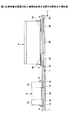
表面実装の一例について、図1乃至図6を用いて説明する。図1は第1従来例である電子装置を示しており、図2は第1従来例である電子装置に用いられている基板3を示している。基板3は、表面に実装部品1A,1Bがはんだ付けされるフットパターン4A,4Bが形成されている。また、基板3の表面には、フットパターン4A,4Bの他にも種々の配線パターン(図示せず)が形成されており、この配線パターンを保護するために基板3の表面にはソルダーレジスト5が形成されている。
An example of surface mounting will be described with reference to FIGS. FIG. 1 shows an electronic device as a first conventional example, and FIG. 2 shows a
ソルダーレジスト5は絶縁性を有した樹脂であり、フットパターン4A,4Bと対向する位置には、図2に示すように開口部7A,7Bが形成されている。従って、ソルダーレジスト5の開口部7A,7Bの形成位置においては、フットパターン4A,4Bが露出した状態となっている。
The
実装部品1A,1Bは、このソルダーレジスト5の開口部7A,7Bから露出したフットパターン4A,4Bにはんだ6を用いて表面実装される。具体的には、実装部品1Aはセラミックチップ部品であるため、その両側部に実装部品電極2Aが設けられている。また、実装部品1Bは発振子等の電子素子であり下面に実装部品電極2Bが形成されている。そして、実装時にはフットパターン4A,4Bにはんだペーストを配設しておき、このはんだペーストが配設された各フットパターン4A,4B上に各電極2A,2Bが位置するよう実装部品1A,1Bを基板3に搭載する。この状態でリフロー処理を行うことにより、実装部品1A,1Bは基板3にはんだ6により表面実装される。
The
図4に示す電子装置も、図1に示した電子装置と略同一の構成である。しかしながら、図1に示した電子装置は、ソルダーレジスト5に形成された開口部7A,7Bの面積がフットパターン4A,4Bの面積よりも小さく、フットパターン4A,4Bの外周部分がソルダーレジスト5により覆われた構成とされている。これに対して図4に示した電子装置は、ソルダーレジスト5に形成された開口部7A,7Bの面積がフットパターン4A,4Bの面積よりも大きく、よってフットパターン4A,4Bはその全部がソルダーレジスト5から露出した構成とされている(図5参照)。
ところで、従来の電子装置では、図1及び図4に示されるように、基板3上に実装部品1A,1Bが露出された状態で、換言するとむき出しの状態で実装される構造のものが多かった。しかしながら、このむき出しの実装構造では、実装部品1A,1Bや配線パターンの配置や構造が簡単にわかってしまい、ノウハウの保護の点から問題があった。
By the way, as shown in FIGS. 1 and 4, many conventional electronic devices have a structure in which the
これを防止する手段としては、図3及び図6に示すように、実装部品(図3及び図6では実装部品1Aのみを示す)を封止樹脂9により封止することが考えられる。このように構成した電子装置10A,10では、封止樹脂9として不透明樹脂を用いることにより、実装部品1A,1Bや配線パターンの配置や構造を外部から見られないようにすることができる。
As means for preventing this, as shown in FIGS. 3 and 6, it is conceivable to seal the mounting component (only the
しかしながら、基板3に実装された実装部品1Aは、ソルダーレジスト5との間に微小な間隙(各図に矢印Δhで示す)が形成されている。この間隙Δhの大きさは、実装部品1Aの大きさやはんだ6の配設量等によりばらつきがあるが、例えば5〜10μm程度の間隙となる。
However, a minute gap (indicated by an arrow Δh in each figure) is formed between the
このように実装部品1Aとソルダーレジスト5(基板3)との間に微細な間隙が形成された場合、封止樹脂9の形成時にこの微細な間隙までは封止樹脂9が入り込めず、よって実装部品1Aとソルダーレジスト5との間に封止樹脂9の存在しない空隙が発生してしまう。
Thus, when a fine gap is formed between the
このように封止樹脂9内に空隙が発生すると、電子装置10A,10Bの実装時に加熱処理が行なわれてはんだ6が溶融した場合には、はんだ6の周囲は封止樹脂9で封止されているため、溶融したはんだ6は間隙内に侵入し、実装部品電極2A間で短絡が発生してしまうおそれがある。また、加熱により間隙内の空気が膨張してしまい、封止樹脂9にクラックが発生するおそれもある。
When the voids are generated in the sealing resin 9 as described above, when the
本発明は上記の点に鑑みてなされたものであり、実装部品と基板との離間距離を大きくすることにより、加熱時において電極パターン間に短絡が発生することを防止しうると共に封止樹脂内にクラックが発生することを防止しうる電子装置を提供することを目的とする。 The present invention has been made in view of the above points, and by increasing the separation distance between the mounting component and the substrate, it is possible to prevent a short circuit from occurring between the electrode patterns during heating, and to ensure that the inside of the sealing resin and to provide an electronic equipment in which a crack can be prevented from being generated on.
上記の課題を解決するために本発明では、次に述べる各手段を講じたことを特徴とするものである。 In order to solve the above-described problems, the present invention is characterized by the following measures.
請求項1記載の発明は、
表面に電極パターン及びソルダーレジストが設けられると共に、該ソルダーレジストに形成された開口から前記電極パターンの一部が露出する構成とされた基板と、
はんだを用いて実装部品電極を前記電極パターンに接合することにより前記基板に実装される実装部品と、
前記基板上に形成され、前記実装部品を封止する封止樹脂とを有し、
前記はんだの一部が前記ソルダーレジストの上部に乗り上げた構成とした電子装置であって、
前記ソルダーレジストは、前記基板を平面視した場合に、前記実装部品電極と前記電極パターンとが対向する領域に重畳するオーバーラップ部を有し、
前記電極パターンの前記開口から露出する部分が、前記オーバーラップ部より内側に位置するよう構成したことを特徴とするものである。
The invention described in
An electrode pattern and a solder resist are provided on the surface, and a substrate configured to expose a part of the electrode pattern from an opening formed in the solder resist;
A mounting component mounted on the substrate by bonding a mounting component electrode to the electrode pattern using solder; and
A sealing resin that is formed on the substrate and seals the mounting component;
An electronic device in which a part of the solder rides on top of the solder resist ,
The solder resist has an overlap portion that overlaps a region where the mounting component electrode and the electrode pattern face each other when the substrate is viewed in plan view,
The portion exposed from the opening of the electrode pattern is configured to be located inside the overlap portion .
上記発明によれば、はんだの一部がソルダーレジストの上部に乗り上げた構成となるため、実装部品と基板との離間距離を大きく取ることができるため、封止樹脂を確実に実装部品と基板との間に導入させることができる。 According to the above invention, since a part of the solder rides on the upper part of the solder resist, the separation distance between the mounting component and the substrate can be increased, so that the sealing resin can be securely attached to the mounting component and the substrate. Can be introduced in between.
また、ソルダーレジストに実装部品電極と電極パターンとが対向する領域に重畳するオーバーラップ部を形成したことにより、容易にはんだの一部をソルダーレジスト(オーバーラップ部)の上部に乗り上げさせることができる。 In addition, by forming an overlap portion that overlaps the region where the mounting component electrode and the electrode pattern face each other on the solder resist, a part of the solder can be easily carried on the upper portion of the solder resist (overlap portion). .
また、請求項2記載の発明は、
請求項1記載の電子装置において、
前記実装部品と前記基板とが対向する部位における前記ソルダーレジストを除去したことを特徴とするものである。
The invention according to
The electronic device according to
The solder resist is removed from a portion where the mounting component and the substrate face each other.
上記発明によれば、実装部品と基板とが直接対向し、両者間にソルダーレジストが存在しないため、実装部品の基板からの高さを更に大きく取ることができ、封止樹脂をより確実に実装部品と基板との間に導入させることができる。 According to the above invention, the mounting component and the board are directly opposed to each other, and there is no solder resist between them, so that the height of the mounting part from the board can be further increased, and the sealing resin is more reliably mounted. It can be introduced between the component and the substrate.
また、請求項3記載の発明は、
請求項1または2記載の電子装置において、
前記基板の表面に複数設けられた前記電極パターンの間に、レジスト材により保護された配線パターンを設けたことを特徴とする電子装置。
また、請求項4記載の発明は、
表面に電極パターン及びソルダーレジストが設けられると共に、該ソルダーレジストに形成された開口から前記電極パターンが露出する構成とされた基板と、
実装部品電極が、前記電極パターンの開口から露出した部分にはんだにより接合されることにより、前記基板に実装される実装部品と、
前記基板上に形成され、前記実装部品を封止する封止樹脂とを有し、
前記電極パターンの中央位置に、前記はんだに埋設される被埋設部材を設けたことを特徴とするものである。
The invention according to
The electronic device according to
An electronic device comprising a wiring pattern protected by a resist material between a plurality of the electrode patterns provided on the surface of the substrate.
The invention according to
An electrode pattern and a solder resist are provided on the surface, and a substrate configured to expose the electrode pattern from an opening formed in the solder resist;
A mounting component electrode is mounted on the substrate by being bonded to the portion exposed from the opening of the electrode pattern by solder, and
A sealing resin that is formed on the substrate and seals the mounting component;
A buried member to be buried in the solder is provided at the center position of the electrode pattern.
上記発明によれば、電極パターンにはんだに埋設される被埋設部材を設けたことにより、電極パターンにはんだを配設した際に埋設部材ははんだの内部に埋設されるため、はんだの高さは被埋設部材を設けないときの高さに比べて高くなる。これにより、実装部品と基板との離間距離を大きく取ることができるため、封止樹脂を確実に実装部品と基板との間に導入させることができる。 According to the above invention, since the embedded member embedded in the solder is provided in the electrode pattern, the embedded member is embedded in the solder when the solder is disposed in the electrode pattern. Becomes higher than the height when the embedded member is not provided. Thereby, since the separation distance of a mounting component and a board | substrate can be taken large, sealing resin can be reliably introduced between a mounting component and a board | substrate.
また、請求項5記載の発明は、
請求項4記載の電子装置において、
前記被埋設部材を前記ソルダーレジストにより形成したことを特徴とするものである。
The invention according to
The electronic device according to
The embedded member is formed of the solder resist.
上記発明によれば、被埋設部材をソルダーレジストにより形成したことにより、被埋設部材をソルダーレジストの形成時に同時形成することが可能となる。 According to the above invention, since the embedded member is formed of the solder resist, the embedded member can be formed simultaneously with the formation of the solder resist.
また、請求項6記載の発明は、
請求項4または5記載の電子装置において、
前記被埋設部材は、前記基板を平面視した場合に、前記実装部品電極と前記電極パターンとが対向する領域に設けられていることを特徴とするものである。
Further, the invention described in
The electronic device according to
The embedded member is provided in a region where the mounting component electrode and the electrode pattern face each other when the substrate is viewed in plan.
上記発明によれば、実装部品電極と電極パターンとが対向する領域に被埋設部材が設けられるため、被埋設部材を確実にはんだ内に埋設することができる。 According to the above invention, since the embedded member is provided in the region where the mounting component electrode and the electrode pattern face each other, the embedded member can be reliably embedded in the solder.
また、請求項7記載の発明は、
請求項4乃至6のいずれか一項に記載の電子装置において、
前記基板の表面に複数設けられた前記電極パターンの間に、レジスト材により保護された配線パターンを設けたことを特徴とするものである。
The invention according to claim 7
The electronic device according to any one of
A wiring pattern protected by a resist material is provided between the plurality of electrode patterns provided on the surface of the substrate .
本発明によれば、実装部品と基板との離間距離を大きく取ることができるため、封止樹脂を確実に実装部品と基板との間に導入させることができ、よって封止樹脂を形成しても実装部品と基板との間に間隙が生じることはない。これにより、この間隙内にはんだが侵入して実装部品電極間で短絡が発生することを防止できると共に、この間隙内の空気が加熱により膨張して封止樹脂等に悪影響を及ぼすことを防止でき、よって電子装置の信頼性を高めることができる。 According to the present invention, since the separation distance between the mounting component and the substrate can be increased, the sealing resin can be reliably introduced between the mounting component and the substrate, and thus the sealing resin is formed. However, there is no gap between the mounted component and the board. As a result, it is possible to prevent the solder from entering the gap and causing a short circuit between the mounting component electrodes, and it is possible to prevent the air in the gap from expanding due to heating and adversely affecting the sealing resin or the like. Therefore, the reliability of the electronic device can be improved.
次に、本発明を実施するための最良の形態について図面と共に説明する。 Next, the best mode for carrying out the present invention will be described with reference to the drawings.
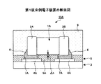
図7乃至図9は、本発明の第1実施例である電子装置30Aを説明するための図である。図7は電子装置30Aの封止樹脂29を配設する前の状態を示す側面図であり、図8は電子装置30Aを構成する基板23の平面図であり、図9は本電子装置30Aの側断面図である。
7 to 9 are diagrams for explaining the
電子装置30Aは、大略すると実装部品20A,20B、基板23、及び封止樹脂29等により構成されている。実装部品20Aは、例えば抵抗やコンデンサー等のセラミックチップ部品であり、両側部に実装部品電極22Aが形成されている。また、実装部品20Bは、例えばSAWフィルターや発振子等の電子素子であり、下面に実装部品電極22Bが形成されている。
In brief, the
基板23は例えばプリント配線基板であり、その表面にフットパターン24A,24Bが形成されている。フットパターン24Aは実装部品20Aを実装するための電極パターンであり、またフットパターン24Bは実装部品20Bを実装するための電極パターンである。また、基板23の表面には、フットパターン24A,24Bの他にも種々の配線パターン31が形成されている。尚、本実施例では、配線パターン31は実装部品20Bと対向する位置にも配設されている。
The
ソルダーレジスト25は、この配線パターン31を保護するため、基板23の表面に形成されている。ソルダーレジスト25は、はんだ付けを行う場合に、フットパターン24A,24B以外の導体(例えば、配線パターン31)にはんだ26が付着しないよう基板23の表面に配設されるものである。このソルダーレジスト25は、スクリーン印刷等により比較的容易に所望の形状で形成することができる。
The solder resist 25 is formed on the surface of the
図8に示すように、ソルダーレジスト25には開口部27A,27Bが形成されている。この開口部27A,27Bは、基板23に形成されているフットパターン24A,24Bの形成位置に対応して形成されている。具体的には、開口部27Aは実装部品20Aを実装するフットパターン24Aに対応して形成されており、開口部27Bは実装部品20Bを実装するフットパターン24Bに対応して形成されている。
As shown in FIG. 8 , openings 27 </ b> A and 27 </ b> B are formed in the solder resist 25. The
また、開口部27Aの図中矢印X方向の長さL1は、実装状態における実装部品20Aの矢印X方向の長さL2よりも短くなるよう構成されている(L2>L1)。また、開口部27Bは実装部品20Bの下部レジスト25Aを挟んで図8中左右に分かれて2個形成されているが、2個の開口部27Bを含めた図中左端部と右端部との長さL3は、実装状態における実装部品20B(図8では、外形を二点鎖線で示す)の矢印X方向の長さL4よりも短くなるよう構成されている(L4>L3)。
Further, the length L1 of the
ここで、各フットパターン24A,24Bとソルダーレジスト25との関係に注目する。本実施例では、フットパターン24A,24Bの一部がソルダーレジスト25により覆われた構成とされている。以下、このソルダーレジスト25のフットパターン24Aを一部覆う部分をオーバーラップ部32Aといい、ソルダーレジスト25のフットパターン24Bを一部覆う部分をオーバーラップ部32Bというものとする。
Here, attention is paid to the relationship between the
この各オーバーラップ部32A,32Bは、各フットパターン24A,24Bの外側位置に設けられている。本実施例においては、オーバーラップ部32Aは図中矢印X方向にのみ延在するよう設けられており、その幅寸法は図中矢印X1で示す幅とされている。
The
このオーバーラップ部32A,32Bは、実装状態における実装部品20A,20Bの領域(図8に二点鎖線で示す領域)の内部に位置するよう構成されている。換言すると、実装部品20A,20Bを基板23に実装した際、オーバーラップ部32A,32Bは実装部品20A,20Bと対向するよう構成されている。
The
また本実施例では、一対のフットパターン24A,24Aの間におけるソルダーレジスト25は、除去された構成となっている。よって、図7に示すように、封止樹脂29による封止前の状態では、実装部品20Aは基板23に直接対向した状態となっている。
In this embodiment, the solder resist 25 between the pair of
これに対して、実装部品20Bの配設側では、左右のフットパターン24Bの間に配線パターン31が配設されている。この配線パターン31を保護するため、実装部品20Bの配設側においては左右のフットパターン24Bの間に下部レジスト25Aが形成された構成とされている。
On the other hand, the
実装部品20A,20Bを基板23に実装するには、フットパターン24A,24B上にはんだペーストを配設する。この際、ハンダペーストは、フットパターン24A,24Bの上部ばかりではなく、オーバーラップ部32Aの上部にも配設する。
In order to mount the mounting
次に、このはんだペーストが配設された各フットパターン24A,24B上に各電極22A,22Bが位置するよう位置決めを行い、その上で実装部品20A,20Bを基板23に装着する。この状態で、実装部品20A,20Bははんだペーストにより基板23に仮止めされる。
Next, positioning is performed so that the
続いて、この実装部品20A,20Bが仮止めされた基板23をリフロー炉に装着し、リフロー処理を行う。これにより、はんだペースト内の有機成分は気化し、またはんだは溶融する。そして、溶融したはんだ26が冷却固化することにより、実装部品20A,20Bの実装部品電極22A,22Bは、はんだ26によりフットパターン24A,24Bにはんだ付けされる。
Subsequently, the
図7は、実装部品20A,20Bが、はんだ26によりフットパターン24A,24Bに固定された状態を示している。ここで、本実施例におけるはんだ26に注目すると、本実施例では、はんだ26の一部がソルダーレジスト25の上部に乗り上げた構成となっている(以下、はんだ26がソルダーレジスト25の上部に乗り上げた部分を乗り上げ部26A,26Bというものとする)。
FIG. 7 shows a state in which the mounting
このように、はんだ26の一部がソルダーレジストの上部に乗り上げた構成となるため、実装状態で実装部品20Aはソルダーレジスト25の表面に対して乗り上げ部26Aの厚さ(図7に矢印ΔH1で示す)だけ高くなり、同様に実装部品20Bはソルダーレジスト25の表面に対して乗り上げ部26Bの厚さ(図7に矢印ΔH2で示す)だけ高くなる。
As described above, since a part of the
この乗り上げ部26A,26Bの厚さ(ΔH1、ΔH2)は、フットパターン24A,24B上でオーバーラップするオーバーラップ部32A,32Bの面積(換言すると、フットパターン24A,24Bの露出面積)や、はんだ26の配設量等により調整することが可能である。
The thicknesses (ΔH1, ΔH2) of the
また、もともとはんだとの親和性の低いソルダーレジスト25上に乗り上げ部26A,26B(はんだ26)を形成するには、フットパターン24A,24Bの外部に露出した部分が、実装部品20A,20Bの実装領域(図8に二点鎖線で示す)よりも外側にないように、返って実装部品20A,20Bの実装領域のなるべく内側に位置するようにすることが重要である。また、オーバーラップ部32A,32Bは、実装部品20A,20Bを実装した状態の基板23を平面視した場合に、実装部品電極22A,22Bとフットパターン24A,24Bとが対向する領域と重畳領域に配設することが重要である。
Further, in order to form the run-up
上記の構成とすることにより、乗り上げ部26A,26Bが実装部品20A,20Bの外周から外部に漏れ出すことを防止でき、よって乗り上げ部26A,26Bを実装部品20A,20Bと基板23(フットパターン24A,24B、オーバーラップ部32A,32B)との間に保持させることができる。
With the above configuration, it is possible to prevent the riding-up
よって、従来(図1乃至図6参照)に比べて、実装部品20A,20Bを基板23に対して大きく離間させることが可能となる。具体的には、実装部品20Aの実装側においては、実装部品20Aの実装位置の下部のソルダーレジスト25も除去されているため、基板23と実装部品20Aとの離間距離は図7に矢印Z1で示す距離となる。
Therefore, compared with the conventional case (see FIGS. 1 to 6), the mounting
また、実装部品20Bの実装側においては、実装部品20Bと基板23との間に配線パターン31の存在により下部レジスト25Aが形成されているが、この下部レジスト25Aの表面と実装部品20Bの下面との間の離間距離は図中矢印Z2で示す距離となる。
On the mounting side of the mounting
いずれの離間距離Z1,Z2も、従来(図3及び図6に示すΔH)に比べて大きくすることができる。具体的には、実装部品20A,20の大きさ、フットパターン24Aの露出面積、はんだ26の配設量等により変動はするものの、例えば離間距離Z1,Z2は20μm〜30μmとすることができる。
Any of the separation distances Z1 and Z2 can be made larger than the conventional distance (ΔH shown in FIGS. 3 and 6). Specifically, the distances Z1 and Z2 can be set to 20 μm to 30 μm, for example, although they vary depending on the size of the mounting
封止樹脂29は、図9に示すように、基板23に配設された実装部品20A,20Bを封止するように形成される。この封止樹脂29はエポキシ系の樹脂であり、例えばトランスファーモールド法を用いて形成される。
As shown in FIG. 9, the sealing
本実施例では、上記のように、実装部品20A,20Bと基板23との離間距離Z1,Z2を大きく取ることができるため、封止樹脂29を確実に実装部品20A,20Bと基板23との間に導入させることができる。特に、実装部品20Aの実装側では、実装部品20Aと基板23との間にソルダーレジスト25が存在しないため、より確実に封止樹脂29を導入させることができる。
In the present embodiment, as described above, the separation distances Z1 and Z2 between the mounting
このように本実施例に係る電子装置30Aでは、封止樹脂29は実装部品20A,20Bと基板23との間に導入されるため、実装部品20A,20Bと基板23との間に間隙が発生するようなことはない。よって、電子装置30Aの実装時等において加熱が行なわれても、各フットパターン24A,24B間ではんだ26による短絡が発生することはなく、また間隙内の空気が膨張して封止樹脂29に悪影響を及ぼすようなこともない。よって、電子装置30Aの信頼性を高めることができる。
As described above, in the
図10は、上記した本発明の第1実施例の変形例である電子装置に設けられる基板23を示している。図8に示した第1実施例においては、オーバーラップ部32A,32Bが図中矢印X方向にのみ延在するよう設けた構成とした。これに本変形例では、オーバーラップ部32A,32Bが図中矢印X方向ばかりでなく、図中矢印Y方向にも延在するよう設けたことを特徴とするものである。
FIG. 10 shows a
図8に示す例では、オーバーラップ部32A,32Bの、矢印Y方向にも延在している部分の幅寸法は図中矢印Y1,Y2で示す幅とされている。本変形例のように、オーバーラップ部32A,32Bの形成位置は、フットパターン24A,24Bの一辺に限定されるものではなく、二辺に形成されてもよいものである。
In the example shown in FIG. 8, the width dimension of the
続いて、本発明の第2実施例について説明する。 Next, a second embodiment of the present invention will be described.
図11乃至図13は、本発明の第2実施例である電子装置30Bを説明するための図である。尚、図11乃至図13において、図7乃至図9に示した第1実施例に係る電子装置30Aと同一構成については同一符号を付し、その説明を省略するものとする。
11 to 13 are diagrams for explaining an
前記した第1実施例に係る電子装置30Aでは、はんだ26の一部がソルダーレジスト25の上部に乗り上げて乗り上げ部26A,26Bを形成することにより、実装部品20A,20Bの基板23に対する高さを高くし、これにより封止樹脂29を確実に実装部品20A,20Bと基板23との間に導入させるようにしたことを特徴としている。
In the
これに対して本実施例に係る電子装置30Aでは、フットパターン24A,24Bにはんだ26に埋設される被埋設部材35を設けたことを特徴とするものである。この被埋設部材35は、ソルダーレジスト25の形成時に一括的に形成されるものであり、よってソルダーレジスト25と同一材質のものである。
On the other hand, the
また、被埋設部材35の形成位置は、図12に示すように、各フットパターン24A,Bの略中央位置に選定されている。前記のように、ソルダーレジスト25はスクリーン印刷等により容易に形成できるものであり、その印刷(配設)位置も自由度を持って選定することができる。
Further, the formation position of the embedded
よって、被埋設部材35をフットパターン24A,24Bの略中央位置に容易に形成することができる。また、被埋設部材35はソルダーレジスト25と同時形成されるため、電子装置30Bの製造工程の簡単化を図ることができる。
Therefore, the embedded
また、本実施例では、フットパターン24A,24Bにオーバーラップ部32A,32Bは設けられておらず、図11及び図12に示すように、各フットパターン24A,24Bは、各開口部28A,28B内に全て露出した構成とされている。
In this embodiment, the
次に、上記のように被埋設部材35が配設されたフットパターン24A,24Bを有する基板23に、実装部品20A,20Bを実装する処理について説明する。実装部品20A,20Bを実装時するには、先ず被埋設部材35が配設されたフットパターン24A,24Bにはんだペーストを配設する。この際、被埋設部材35を覆うようにはんだペーストを配設する。
Next, a process of mounting the mounting
次に、各フットパターン24A,24B上に各電極22A,22Bが位置するよう基板23に対して実装部品20A,20Bの位置決めを行い、その上で実装部品20A,20Bを基板23に搭載装着する。この状態で、実装部品20A,20Bははんだペーストにより基板23に仮止めされる。
Next, the mounting
続いて、この基板23をリフロー炉に装着してリフロー処理を行う。これにより、はんだペースト内の有機成分は気化し、またはんだは溶融する。そして、溶融したはんだ26が冷却固化することにより、実装部品20A,20Bの実装部品電極22A,22Bは、はんだ26によりフットパターン24A,24Bにはんだ付けされる。
Subsequently, the
はんだ26が溶融した際、被埋設部材35はフットパターン24A,24Bの略中央に設けられているため、溶融したはんだ26は表面張力により球に近い形状になろうとする。このため、ソルダーレジスト材からなる被埋設部材35であっても、被埋設部材35ははんだ26の内部に位置した状態となる。そして、この状態ではんだ26が冷却されることにより、被埋設部材35ははんだ26内に埋設された状態となる。
When the
このように、被埋設部材35がはんだ26内に埋設されることにより、はんだ26の高さは被埋設部材35を設けないときの高さに比べて高くなる。即ち、被埋設部材35の体積に相当する分だけ、はんだ26の高さが高くなる。よって、本実施例に係る電子装置30Bにおいても、実装部品20A,20Bと基板23との離間距離を大きく取ることが可能となり、よって封止樹脂29を確実に実装部品20A,20Bと基板23との間に導入させることができる。
As described above, since the embedded
よって、本実施例に係る電子装置30Bにおいても、第1実施例に係る電子装置30Aと同様に、実装部品20A,20Bと基板23との間に間隙が発生するようなことはない。よって、電子装置30Aの実装時等において加熱が行なわれても、各フットパターン24A,24B間ではんだ26による短絡が発生することはなく、また間隙内の空気が膨張して封止樹脂29に悪影響を及ぼすようなこともない。よって、電子装置30Bの信頼性を高めることができる。
Therefore, in the
続いて、本発明の第3実施例について説明する。 Subsequently, a third embodiment of the present invention will be described.
図14は本発明の第3実施例である電子装置30Cの断面図であり、図15乃至図17は電子装置30Cの製造方法を説明するための図である。尚、本実施例の説明に用いる図15乃至図17においても、図7乃至図9に示した第1実施例に係る電子装置30Aと同一構成については同一符号を付し、その説明を省略するものとする。
FIG. 14 is a cross-sectional view of an electronic device 30C according to a third embodiment of the present invention, and FIGS. 15 to 17 are views for explaining a method of manufacturing the electronic device 30C. 15 to 17 used in the description of this embodiment, the same components as those of the
本実施例に係る電子装置30Cは、実装部品20A,20Bと基板23との間にアンダーフィル樹脂36を配設したことを特徴とするものである。このアンダーフィル樹脂36は、隣接するフットパターン24A間及び隣接するフットパターン24B間に配設された下部レジスト25Aと実装部品20A,20Bとの離間部分に配設される。このため、実装状態において、実装部品20A,20Bと基板23との間はアンダーフィル樹脂36で埋められた状態となり間隙が形成されるようなことはない。
The
よって、電子装置30Cの実装時等において加熱が行なわれても、各フットパターン24A,24B間ではんだ26による短絡が発生することはなく、また間隙内の空気が膨張して封止樹脂29に悪影響を及ぼすようなこともない。よって、電子装置30Bの信頼性を高めることができる。
Therefore, even if heating is performed at the time of mounting the electronic device 30C or the like, there is no short circuit due to the
続いて、電子装置30Cの製造方法について説明する。電子装置30Cを製造するには、予め所定のパターンでフットパターン24A,24Bが形成されると共に、ソルダーレジスト25に所定の形状の開口部27A,27Bが形成された基板23を用意する。本実施例では、フットパターン24A,24Bはソルダーレジスト25に形成された開口部27A,27Bから全て露出した構成とされている。
Next, a method for manufacturing the electronic device 30C will be described. In order to manufacture the electronic device 30C, a
この基板23に対し、先ずはんだペースト37を配設する処理を実施する(はんだ配設工程)。このはんだ配設工程では、スクリーン印刷法を用いてはんだペースト37を開口部27A,27Bから露出したフットパターン24A,24B上に印刷する。図15は、フットパターン24A,24B上にスクリーン印刷法を用いてはんだペースト37を配設した状態を示している。
The
続いて、はんだペースト37が配設されたフットパターン24A,24B上に実装部品20A,20Bを配設する。具体的には、実装部品20Aの実装部品電極22Aとフットパターン24Aとを位置決めし、実装部品20Bの実装部品電極22Bとフットパターン24Bとを位置決めし、実装部品電極22A,22Bをはんだペースト37に押し付ける。これにより、実装部品20A,20Bははんだペースト37の有する接着力により基板23に仮止めされた状態となる。
Subsequently, the mounting
続いて、実装部品20A,20Bが仮止めされた基板23は、リフロー炉に装着されて加熱される。これにより、はんだペースト37内の有機成分は気化すると共にはんだは溶融する。そして、冷却を行うことにより、実装部品電極22A,22Bはフットパターン24A,24Bにはんだ26により固定された状態となる(実装工程)。図16は、実装工程が終了し、実装部品電極22A,22Bがはんだ26により基板23に実装された状態を示している。この状態では、実装部品電極22A,22Bと下部レジスト25Aとの間には間隙が形成されている。
Subsequently, the
尚、このリフロー処理による加熱時においては、実装部品20A,20Bは封止樹脂29により封止されていないため、はんだ26は溶融しても自由に移動でき、また膨張しても表面張力によりフットパターン24A.24B上から流出するようなことはない。このため、隣接するフットパターン24A間及びフットパターン24B間ではんだ26による短絡が発生するようなことはない。
During the heating by the reflow process, the mounting
続いて、実装部品電極22A,22Bと基板23(下部レジスト25A)との間に形成されている間隙にアンダーフィル樹脂36を充填する(アンダーフィル充填工程)。このアンダーフィル樹脂36の充填処理は、例えばディスペンサーを用いて行うことができる。図17は、アンダーフィル充填工程が終了した基板23を示している。
Subsequently, an
続いて、実装部品電極22A,22Bと下部レジスト25Aとの間にアンダーフィル樹脂36が充填された基板23に対し、実装部品電極22A,22Bを封止するよう封止樹脂29を形成する(封止工程)。この封止樹脂29はエポキシ系の樹脂であり、例えばトランスファーモールド法を用いて形成される。この際、前記のように実装部品電極22A,22Bと下部レジスト25Aとの間にアンダーフィル樹脂36が充填されているため、封止樹脂29内に間隙が形成されるようなことはない。以上の一連の工程を経ることにより、図14に示す電子装置30Cが製造される。
Subsequently, a sealing
続いて、本発明の第4実施例について説明する。 Subsequently, a fourth embodiment of the present invention will be described.
図18は本発明の第4実施例である電子装置30Dの断面図であり、図19乃至図21は電子装置30Dの製造方法を説明するための図である。尚、本実施例の説明に用いる図19乃至図21においても、図7乃至図9に示した第1実施例に係る電子装置30Aと同一構成については同一符号を付し、その説明を省略するものとする。
FIG. 18 is a cross-sectional view of an electronic device 30D according to a fourth embodiment of the present invention, and FIGS. 19 to 21 are views for explaining a method of manufacturing the electronic device 30D. 19 to 21 used for the description of the present embodiment, the same components as those in the
本実施例に係る電子装置30Dは、実装部品20A,20Bと基板23との間にフラックスフィル樹脂38を配設したことを特徴とするものである。このフラックスフィル樹脂38は、はんだ付けに必要な活性力を有する熱硬化可能な接着剤である。具体的には、加熱されることにより硬化して接着剤としての機能を奏すると共に、加熱によりはんだ表面の酸化膜を除去すると共にはんだ溶融時における流動性を高める活性剤としての機能を奏するものである。
The electronic apparatus 30D according to the present embodiment is characterized in that a
このフラックスフィル樹脂38は、隣接するフットパターン24A間及び隣接するフットパターン24B間に配設された下部レジスト25Aと実装部品20A,20Bとの離間部分に配設される。このため、実装状態において、実装部品20A,20Bと基板23との間はフラックスフィル樹脂38で埋められた状態となり間隙が形成されるようなことはない。
The flux fill
よって、本実施例に係る電子装置30Dの実装時等において加熱が行なわれても、各フットパターン24A,24B間ではんだ26による短絡が発生することはなく、また間隙内の空気が膨張して封止樹脂29に悪影響を及ぼすようなこともない。よって、電子装置30Dの信頼性を高めることができる。
Therefore, even if heating is performed during mounting of the electronic device 30D according to the present embodiment, a short circuit due to the
続いて、電子装置30Dの製造方法について説明する。電子装置30Dを製造するには、予め所定のパターンでフットパターン24A,24Bが形成されると共に、ソルダーレジスト25に所定の形状の開口部27A,27Bが形成された基板23を用意する。本実施例では、フットパターン24A,24Bはソルダーレジスト25に形成された開口部27A,27Bから全て露出した構成とされている。
Next, a method for manufacturing the electronic device 30D will be described. In order to manufacture the electronic device 30D, a
この基板23に対し、先ずはんだペースト37を配設する処理を実施する(はんだ配設工程)。このはんだ配設工程では、スクリーン印刷法を用いてはんだペースト37を開口部27A,27Bから露出したフットパターン24A,24B上に印刷する。更に、本実施例ではフットパターン24A,24B上にはんだペースト37が配設された基板23をリフロー炉に装着し加熱処理を行い、はんだペースト37内の有機成分を気化させ、フットパターン24,24B上にはんだ26を形成する(はんだ配設工程)。図19は、フットパターン24A,24B上にはんだ26が形成された基板23を示している。
The
続いて、実装される実装部品20Aの下部位置(隣接するフットパターン24Aの間)及び実装される実装部品20Bの下部位置(隣接するフットパターン24Bの間)にフラックスフィル樹脂38を配設する(フラックスフィル樹脂配設工程)。本実施例では、フラックスフィル樹脂38としてフィルム状のフラックスフィル樹脂を用いている。そして、本実施例では、このフィルム状のフラックスフィル樹脂38を上記の所定位置に配置する。
Subsequently, the flux fill
図20は、このフィルム状のフラックスフィル樹脂38が基板23に配置された状態を示している。同図に示すように、フラックスフィル樹脂38は、フットパターン24A,24Bに形成されているはんだ26の上部を覆うよう配設されている。
FIG. 20 shows a state in which the film-like flux fill
尚、このフラックスフィル樹脂38はフィルム状のものに限定されるものではなく、液状のフラックスフィル樹脂38をポッティング等により上記の所定位置に塗布する構成としてもよい。
The flux fill
続いて、フラックスフィル樹脂38が配設された基板23上に実装部品20A,20Bを配設する。具体的には、実装部品20Aの実装部品電極22Aとフットパターン24Aとを位置決めし、実装部品20Bの実装部品電極22Bとフットパターン24Bとを位置決めし、実装部品電極22A,22Bをフラックスフィル樹脂38に押し付ける。
Subsequently, the mounting
これにより、実装部品20A,20Bはフラックスフィル樹脂38の有する接着力により基板23に仮止めされた状態となる(フラックスフィル樹脂38はこの時点では硬化してない)。また、実装部品20A,20Bの実装部品電極22A,22Bは、はんだ26と当接した状態となる。図21は、実装部品20A,20Bが基板23に仮止めされた状態を示している。
Thus, the mounted
続いて、実装部品20A,20Bが仮止めされた基板23は、リフロー炉に装着されて加熱される。これにより、はんだ26は再び溶融し、その後に冷却を行うことにより、実装部品電極22A,22Bはフットパターン24A,24Bにはんだ26により固定された状態となる(実装工程)。
Subsequently, the
この際、フラックスフィル樹脂38は加熱されることにより熱硬化し、実装部品20Aと基板23とを接着する。このため、実装部品20A,20Bと基板23との固定力は、はんだ26による接合力に加えてフラックスフィル樹脂38による接着力により固定される。このため、実装部品20A,20Bと基板23とを確実に固定することができ、電子装置30Dの機械的な信頼性を高めることができる。
At this time, the flux fill
また、フラックスフィル樹脂38は活性剤を含んでいるため、加熱されることによりはんだ26が溶融する際、はんだ26の表面に形成された酸化膜を除去すると共に溶融時におけるはんだ26の流動性を高める。これにより、実装部品電極22A,22Bとフットパターン24A,24Bをはんだ26により確実に接合することができ、電気的な面においても電子装置30Dの信頼性を高めることができる。
Further, since the flux fill
尚、このリフロー処理による加熱時においては、本実施例においても実装部品20A,20Bは封止樹脂29により封止されていないため、隣接するフットパターン24A間及びフットパターン24B間ではんだ26による短絡が発生するようなことはない。
At the time of heating by this reflow process, the mounting
続いて、実装部品電極22A,22Bと下部レジスト25Aとの間にフラックスフィル樹脂38が介在した基板23に対し、実装部品電極22A,22Bを封止するよう封止樹脂29を形成する(封止工程)。この封止樹脂29はエポキシ系の樹脂であり、例えばトランスファーモールド法を用いて形成される。この際、前記のように実装部品電極22A,22Bと下部レジスト25Aとの間にフラックスフィル樹脂38が充填されているため、封止樹脂29内に間隙が形成されるようなことはない。以上の一連の工程を経ることにより、図18に示す電子装置30Dが製造される。
Subsequently, a sealing
図22及び図23は、第4実施例である電子装置30Dの製造方法の変形例を説明するための図である。前記した電子装置30Dの製造方法では、基板23のフットパターン24A,24Bにはんだペースト37を印刷した後、加熱してはんだ26とした後にフラックスフィル樹脂38及び実装部品20A,20Bを配設する方法とした。
22 and 23 are diagrams for describing a modification of the method for manufacturing the electronic device 30D according to the fourth embodiment. In the manufacturing method of the electronic device 30D described above, the
これに対して本変形例では、図22に示すようにフットパターン24A,24Bにはんだペースト37をスクリーン印刷で印刷した後、下部レジスト25Aの上部にフラックスフィル樹脂38を塗布する。尚、基板23に対するはんだペースト37の印刷と、下部レジスト25Aに対するフラックスフィル樹脂38の塗布は、その順番を変更可能なものである。
On the other hand, in this modified example, as shown in FIG. 22, after the
上記のようにはんだペースト37及びフラックスフィル樹脂38が基板23に配設されると、図23に示すように、実装部品20A,20Bが前記した各実施例同様に基板23に対して位置決めされた上で実装される。これにより、実装部品20A,20Bは、はんだペースト37及びフラックスフィル樹脂38の有する接着剤により基板23に仮止めされる。
When the
続いて、上記のように実装部品20A,20Bが仮止めされた基板23をリフロー炉に装着して加熱処理することにより、実装部品電極22A,22Bとフットパターン24A,24Bははんだ26によりはんだ付けされ、また実装部品20A,20Bと基板23はフラックスフィル樹脂38により接着固定される。これにより、図18に示す電子装置30Dが製造される。
Subsequently, the mounting
20A,20B 実装部品
22A,22B 実装部品電極
23 基板
24A,24B フットパターン
25 ソルダーレジスト
26 はんだ
26A,26B 乗り上げ部
27A,27B,28A,28B 開口部
29 封止樹脂
30A〜30D 電子装置
32A,32B オーバーラップ部
35 被埋設部材
36 アンダーフィル樹脂
37 はんだペースト
38 フラックスフィル樹脂
20A,
Claims (7)
はんだを用いて実装部品電極を前記電極パターンに接合することにより前記基板に実装される実装部品と、
前記基板上に形成され、前記実装部品を封止する封止樹脂とを有し、
前記はんだの一部が前記ソルダーレジストの上部に乗り上げた構成とした電子装置であって、
前記ソルダーレジストは、前記基板を平面視した場合に、前記実装部品電極と前記電極パターンとが対向する領域に重畳するオーバーラップ部を有し、
前記電極パターンの前記開口から露出する部分が、前記オーバーラップ部より内側に位置するよう構成したことを特徴とする電子装置。 An electrode pattern and a solder resist are provided on the surface, and a substrate configured to expose a part of the electrode pattern from an opening formed in the solder resist;
A mounting component mounted on the substrate by bonding a mounting component electrode to the electrode pattern using solder; and
A sealing resin that is formed on the substrate and seals the mounting component;
An electronic device in which a part of the solder rides on top of the solder resist ,
The solder resist has an overlap portion that overlaps a region where the mounting component electrode and the electrode pattern face each other when the substrate is viewed in plan view,
The electronic device is configured such that a portion exposed from the opening of the electrode pattern is positioned inside the overlap portion .
前記実装部品と前記基板とが対向する部位における前記ソルダーレジストを除去したことを特徴とする電子装置。 The electronic device according to claim 1 .
The electronic device according to claim 1, wherein the solder resist is removed from a portion where the mounting component and the substrate face each other.
前記基板の表面に複数設けられた前記電極パターンの間に、レジスト材により保護された配線パターンを設けたことを特徴とする電子装置。An electronic device comprising a wiring pattern protected by a resist material between a plurality of the electrode patterns provided on the surface of the substrate.
実装部品電極が、前記電極パターンの開口から露出した部分にはんだにより接合されることにより、前記基板に実装される実装部品と、
前記基板上に形成され、前記実装部品を封止する封止樹脂とを有し、
前記電極パターンの中央位置に、前記はんだに埋設される被埋設部材を設けたことを特徴とする電子装置。 An electrode pattern and a solder resist are provided on the surface, and a substrate configured to expose the electrode pattern from an opening formed in the solder resist;
The mounting component electrode is bonded to the portion exposed from the opening of the electrode pattern by solder, so that the mounting component mounted on the substrate,
A sealing resin that is formed on the substrate and seals the mounting component;
An electronic device comprising a buried member buried in the solder at a central position of the electrode pattern.
前記被埋設部材を前記ソルダーレジストにより形成したことを特徴とする電子装置。 The electronic device according to claim 4.
An electronic apparatus, wherein the embedded member is formed of the solder resist.
前記被埋設部材は、前記基板を平面視した場合に、前記実装部品電極と前記電極パターンとが対向する領域に設けられていることを特徴とする電子装置。 The electronic device according to claim 4 or 5,
The embedded device is provided in a region where the mounting component electrode and the electrode pattern face each other when the substrate is viewed in plan.
前記基板の表面に複数設けられた前記電極パターンの間に、レジスト材により保護された配線パターンを設けたことを特徴とする電子装置。An electronic device comprising a wiring pattern protected by a resist material between a plurality of the electrode patterns provided on the surface of the substrate.
Priority Applications (6)
| Application Number | Priority Date | Filing Date | Title |
|---|---|---|---|
| JP2005164387A JP4533248B2 (en) | 2005-06-03 | 2005-06-03 | Electronic equipment |
| KR1020060048964A KR20060126368A (en) | 2005-06-03 | 2006-05-30 | Electronic device and method of manufacturing the same |
| EP06252847A EP1729337A3 (en) | 2005-06-03 | 2006-06-01 | Electronic device and method of manufacturing the same |
| US11/421,942 US20060273461A1 (en) | 2005-06-03 | 2006-06-02 | Electronic device and method of manufacturing the same |
| CNA2006100833491A CN1873970A (en) | 2005-06-03 | 2006-06-02 | Electronic device and method of manufacturing the same |
| TW095119564A TW200707671A (en) | 2005-06-03 | 2006-06-02 | Electronic device and method of manufacturing the same |
Applications Claiming Priority (1)
| Application Number | Priority Date | Filing Date | Title |
|---|---|---|---|
| JP2005164387A JP4533248B2 (en) | 2005-06-03 | 2005-06-03 | Electronic equipment |
Publications (2)
| Publication Number | Publication Date |
|---|---|
| JP2006339524A JP2006339524A (en) | 2006-12-14 |
| JP4533248B2 true JP4533248B2 (en) | 2010-09-01 |
Family
ID=37026966
Family Applications (1)
| Application Number | Title | Priority Date | Filing Date |
|---|---|---|---|
| JP2005164387A Expired - Fee Related JP4533248B2 (en) | 2005-06-03 | 2005-06-03 | Electronic equipment |
Country Status (6)
| Country | Link |
|---|---|
| US (1) | US20060273461A1 (en) |
| EP (1) | EP1729337A3 (en) |
| JP (1) | JP4533248B2 (en) |
| KR (1) | KR20060126368A (en) |
| CN (1) | CN1873970A (en) |
| TW (1) | TW200707671A (en) |
Families Citing this family (22)
| Publication number | Priority date | Publication date | Assignee | Title |
|---|---|---|---|---|
| JP2007142355A (en) * | 2005-10-18 | 2007-06-07 | Matsushita Electric Ind Co Ltd | Module with built-in electronic components |
| JP2008218528A (en) * | 2007-02-28 | 2008-09-18 | Fujitsu Ltd | Method for mounting electronic part and production device |
| JP4962217B2 (en) | 2007-08-28 | 2012-06-27 | 富士通株式会社 | Printed wiring board and electronic device manufacturing method |
| JP4788754B2 (en) * | 2008-10-15 | 2011-10-05 | パナソニック株式会社 | Component built-in wiring board and method for manufacturing component built-in wiring board |
| JP5117371B2 (en) * | 2008-12-24 | 2013-01-16 | 新光電気工業株式会社 | Semiconductor device and manufacturing method thereof |
| CN102907187A (en) * | 2010-05-26 | 2013-01-30 | 株式会社村田制作所 | Substrate with built-in component |
| CN103180943B (en) * | 2010-11-04 | 2016-04-13 | 阿尔卑斯电气株式会社 | Electronic component module |
| JP5824679B2 (en) * | 2011-04-14 | 2015-11-25 | パナソニックIpマネジメント株式会社 | Mounting structure |
| JP6024200B2 (en) * | 2012-05-18 | 2016-11-09 | 富士電機機器制御株式会社 | Electronic component mounting method on surface mount board |
| JP5751245B2 (en) * | 2012-11-30 | 2015-07-22 | Tdk株式会社 | Chip component mounting structure and module product using the same |
| WO2014103541A1 (en) * | 2012-12-27 | 2014-07-03 | 日本碍子株式会社 | Electronic component and method for manufacturing same |
| JP6036513B2 (en) | 2013-04-19 | 2016-11-30 | 株式会社デンソー | Vehicle electronics |
| CN107222981B (en) * | 2013-05-20 | 2019-07-02 | 日月光半导体制造股份有限公司 | The manufacturing method of electronic module |
| JP6694311B2 (en) * | 2016-03-31 | 2020-05-13 | Fdk株式会社 | Printed wiring board |
| TWI626723B (en) * | 2017-03-06 | 2018-06-11 | 力成科技股份有限公司 | Package structure |
| DE102017212796A1 (en) * | 2017-07-26 | 2019-01-31 | Robert Bosch Gmbh | Electrical assembly |
| JP7167933B2 (en) | 2017-10-26 | 2022-11-09 | Tdk株式会社 | Structure with built-in electronic components |
| US11282717B2 (en) * | 2018-03-30 | 2022-03-22 | Intel Corporation | Micro-electronic package with substrate protrusion to facilitate dispense of underfill between a narrow die-to-die gap |
| JP7098670B2 (en) * | 2019-03-26 | 2022-07-11 | キヤノン株式会社 | Electronic modules and electronic devices |
| CN113473770B (en) * | 2021-06-11 | 2022-08-05 | 无锡润越机电科技有限公司 | Control cabinet with isolation structure |
| EP4135027A1 (en) * | 2021-08-11 | 2023-02-15 | Murata Manufacturing Co., Ltd. | Surface-mount components, methods of manufacture thereof, and mounting methods employing the components |
| WO2023140075A1 (en) * | 2022-01-24 | 2023-07-27 | 株式会社村田製作所 | Elastic wiring substrate and method for manufacturing elastic wiring substrate |
Citations (2)
| Publication number | Priority date | Publication date | Assignee | Title |
|---|---|---|---|---|
| JPH1098045A (en) * | 1996-09-20 | 1998-04-14 | Nec Corp | Formation of bump electrode |
| JPH1098075A (en) * | 1996-09-20 | 1998-04-14 | Toshiba Corp | Semiconductor mounting method, semiconductor mounting device and semiconductor mounting structure |
Family Cites Families (8)
| Publication number | Priority date | Publication date | Assignee | Title |
|---|---|---|---|---|
| KR0141952B1 (en) * | 1994-12-19 | 1998-06-01 | 문정환 | Semiconductor package and production thereof |
| US20020070443A1 (en) * | 2000-12-08 | 2002-06-13 | Xiao-Chun Mu | Microelectronic package having an integrated heat sink and build-up layers |
| JP2004111676A (en) * | 2002-09-19 | 2004-04-08 | Toshiba Corp | Semiconductor device, manufacturing method thereof, and member for semiconductor package |
| JP4489411B2 (en) * | 2003-01-23 | 2010-06-23 | 新光電気工業株式会社 | Manufacturing method of electronic component mounting structure |
| TWI227099B (en) * | 2003-03-31 | 2005-01-21 | Siliconware Precision Industries Co Ltd | Chip carrier for testing electric performance of passive components and method for testing same |
| JP2005109187A (en) | 2003-09-30 | 2005-04-21 | Tdk Corp | Flip chip packaging circuit board and its manufacturing method, and integrated circuit device |
| JP4559163B2 (en) * | 2004-08-31 | 2010-10-06 | ルネサスエレクトロニクス株式会社 | Package substrate for semiconductor device, method for manufacturing the same, and semiconductor device |
| JP2006351565A (en) * | 2005-06-13 | 2006-12-28 | Shinko Electric Ind Co Ltd | Stacked semiconductor package |
-
2005
- 2005-06-03 JP JP2005164387A patent/JP4533248B2/en not_active Expired - Fee Related
-
2006
- 2006-05-30 KR KR1020060048964A patent/KR20060126368A/en not_active Application Discontinuation
- 2006-06-01 EP EP06252847A patent/EP1729337A3/en not_active Withdrawn
- 2006-06-02 TW TW095119564A patent/TW200707671A/en unknown
- 2006-06-02 US US11/421,942 patent/US20060273461A1/en not_active Abandoned
- 2006-06-02 CN CNA2006100833491A patent/CN1873970A/en active Pending
Patent Citations (2)
| Publication number | Priority date | Publication date | Assignee | Title |
|---|---|---|---|---|
| JPH1098045A (en) * | 1996-09-20 | 1998-04-14 | Nec Corp | Formation of bump electrode |
| JPH1098075A (en) * | 1996-09-20 | 1998-04-14 | Toshiba Corp | Semiconductor mounting method, semiconductor mounting device and semiconductor mounting structure |
Also Published As
| Publication number | Publication date |
|---|---|
| CN1873970A (en) | 2006-12-06 |
| JP2006339524A (en) | 2006-12-14 |
| TW200707671A (en) | 2007-02-16 |
| US20060273461A1 (en) | 2006-12-07 |
| EP1729337A2 (en) | 2006-12-06 |
| EP1729337A3 (en) | 2008-09-10 |
| KR20060126368A (en) | 2006-12-07 |
Similar Documents
| Publication | Publication Date | Title |
|---|---|---|
| JP4533248B2 (en) | Electronic equipment | |
| JPH11214586A (en) | Electronic circuit device | |
| JP2007048976A (en) | Printed circuit board and electronic instrument equipped therewith | |
| JP5604876B2 (en) | Electronic device and manufacturing method thereof | |
| JP2006140327A (en) | Wiring board and method for mounting electronic component using the same | |
| TW201342555A (en) | Solder-mounted board, production method therefor, and semiconductor device | |
| JP5229401B2 (en) | Resin substrate with built-in electronic components and electronic circuit module | |
| JP2009135428A (en) | Mounted structural body and method of manufacturing the same | |
| WO2018084143A1 (en) | Electronic component package, circuit module, and method for producing electronic component package | |
| JP2001244384A (en) | Bare chip mounting printed wiring board | |
| JP7232123B2 (en) | Wiring board, electronic device, and method for manufacturing wiring board | |
| JP2005340448A (en) | Semiconductor device, its manufacturing method, circuit board, and electronic apparatus | |
| JP5159750B2 (en) | Solder balls and semiconductor packages | |
| JP2011108814A (en) | Method of bonding surface mounting electronic component, and electronic device | |
| JP4609435B2 (en) | Component-embedded substrate, electronic device using the same, and manufacturing method used therefor | |
| JP2007059588A (en) | Method of manufacturing wiring board, and wiring board | |
| JP4609434B2 (en) | Component built-in board and electronic equipment using the same | |
| JP2007201356A (en) | Mounting method of shield | |
| KR200478126Y1 (en) | Electric component module | |
| JP2004327743A (en) | Wiring board with solder bump and its producing process | |
| JP3423174B2 (en) | Chip-on-board mounting structure and method of manufacturing the same | |
| JP2008243879A (en) | Electronic device and its manufacturing method | |
| JP5935188B2 (en) | Wiring board and manufacturing method thereof | |
| JP4212880B2 (en) | Circuit board assembly | |
| JP2007266640A (en) | Semiconductor device, method of manufacturing the same, circuit board, and electronic apparatus |
Legal Events
| Date | Code | Title | Description |
|---|---|---|---|
| A621 | Written request for application examination |
Free format text: JAPANESE INTERMEDIATE CODE: A621 Effective date: 20080123 |
|
| A977 | Report on retrieval |
Free format text: JAPANESE INTERMEDIATE CODE: A971007 Effective date: 20100226 |
|
| A131 | Notification of reasons for refusal |
Free format text: JAPANESE INTERMEDIATE CODE: A131 Effective date: 20100309 |
|
| A521 | Request for written amendment filed |
Free format text: JAPANESE INTERMEDIATE CODE: A523 Effective date: 20100507 |
|
| TRDD | Decision of grant or rejection written | ||
| A01 | Written decision to grant a patent or to grant a registration (utility model) |
Free format text: JAPANESE INTERMEDIATE CODE: A01 Effective date: 20100608 |
|
| A01 | Written decision to grant a patent or to grant a registration (utility model) |
Free format text: JAPANESE INTERMEDIATE CODE: A01 |
|
| A61 | First payment of annual fees (during grant procedure) |
Free format text: JAPANESE INTERMEDIATE CODE: A61 Effective date: 20100611 |
|
| R150 | Certificate of patent or registration of utility model |
Ref document number: 4533248 Country of ref document: JP Free format text: JAPANESE INTERMEDIATE CODE: R150 Free format text: JAPANESE INTERMEDIATE CODE: R150 |
|
| FPAY | Renewal fee payment (event date is renewal date of database) |
Free format text: PAYMENT UNTIL: 20130618 Year of fee payment: 3 |
|
| LAPS | Cancellation because of no payment of annual fees |