JP4526257B2 - 半導体発光装置 - Google Patents
半導体発光装置 Download PDFInfo
- Publication number
- JP4526257B2 JP4526257B2 JP2003369568A JP2003369568A JP4526257B2 JP 4526257 B2 JP4526257 B2 JP 4526257B2 JP 2003369568 A JP2003369568 A JP 2003369568A JP 2003369568 A JP2003369568 A JP 2003369568A JP 4526257 B2 JP4526257 B2 JP 4526257B2
- Authority
- JP
- Japan
- Prior art keywords
- light
- resin
- lens
- led chip
- emitting device
- Prior art date
- Legal status (The legal status is an assumption and is not a legal conclusion. Google has not performed a legal analysis and makes no representation as to the accuracy of the status listed.)
- Expired - Fee Related
Links
Images


Classifications
-
- H—ELECTRICITY
- H01—ELECTRIC ELEMENTS
- H01L—SEMICONDUCTOR DEVICES NOT COVERED BY CLASS H10
- H01L2224/00—Indexing scheme for arrangements for connecting or disconnecting semiconductor or solid-state bodies and methods related thereto as covered by H01L24/00
- H01L2224/01—Means for bonding being attached to, or being formed on, the surface to be connected, e.g. chip-to-package, die-attach, "first-level" interconnects; Manufacturing methods related thereto
- H01L2224/42—Wire connectors; Manufacturing methods related thereto
- H01L2224/47—Structure, shape, material or disposition of the wire connectors after the connecting process
- H01L2224/48—Structure, shape, material or disposition of the wire connectors after the connecting process of an individual wire connector
- H01L2224/4805—Shape
- H01L2224/4809—Loop shape
- H01L2224/48091—Arched
-
- H—ELECTRICITY
- H01—ELECTRIC ELEMENTS
- H01L—SEMICONDUCTOR DEVICES NOT COVERED BY CLASS H10
- H01L2224/00—Indexing scheme for arrangements for connecting or disconnecting semiconductor or solid-state bodies and methods related thereto as covered by H01L24/00
- H01L2224/01—Means for bonding being attached to, or being formed on, the surface to be connected, e.g. chip-to-package, die-attach, "first-level" interconnects; Manufacturing methods related thereto
- H01L2224/42—Wire connectors; Manufacturing methods related thereto
- H01L2224/47—Structure, shape, material or disposition of the wire connectors after the connecting process
- H01L2224/48—Structure, shape, material or disposition of the wire connectors after the connecting process of an individual wire connector
- H01L2224/481—Disposition
- H01L2224/48151—Connecting between a semiconductor or solid-state body and an item not being a semiconductor or solid-state body, e.g. chip-to-substrate, chip-to-passive
- H01L2224/48221—Connecting between a semiconductor or solid-state body and an item not being a semiconductor or solid-state body, e.g. chip-to-substrate, chip-to-passive the body and the item being stacked
- H01L2224/48245—Connecting between a semiconductor or solid-state body and an item not being a semiconductor or solid-state body, e.g. chip-to-substrate, chip-to-passive the body and the item being stacked the item being metallic
- H01L2224/48247—Connecting between a semiconductor or solid-state body and an item not being a semiconductor or solid-state body, e.g. chip-to-substrate, chip-to-passive the body and the item being stacked the item being metallic connecting the wire to a bond pad of the item
-
- H—ELECTRICITY
- H01—ELECTRIC ELEMENTS
- H01L—SEMICONDUCTOR DEVICES NOT COVERED BY CLASS H10
- H01L2224/00—Indexing scheme for arrangements for connecting or disconnecting semiconductor or solid-state bodies and methods related thereto as covered by H01L24/00
- H01L2224/01—Means for bonding being attached to, or being formed on, the surface to be connected, e.g. chip-to-package, die-attach, "first-level" interconnects; Manufacturing methods related thereto
- H01L2224/42—Wire connectors; Manufacturing methods related thereto
- H01L2224/47—Structure, shape, material or disposition of the wire connectors after the connecting process
- H01L2224/48—Structure, shape, material or disposition of the wire connectors after the connecting process of an individual wire connector
- H01L2224/481—Disposition
- H01L2224/48151—Connecting between a semiconductor or solid-state body and an item not being a semiconductor or solid-state body, e.g. chip-to-substrate, chip-to-passive
- H01L2224/48221—Connecting between a semiconductor or solid-state body and an item not being a semiconductor or solid-state body, e.g. chip-to-substrate, chip-to-passive the body and the item being stacked
- H01L2224/48245—Connecting between a semiconductor or solid-state body and an item not being a semiconductor or solid-state body, e.g. chip-to-substrate, chip-to-passive the body and the item being stacked the item being metallic
- H01L2224/48257—Connecting between a semiconductor or solid-state body and an item not being a semiconductor or solid-state body, e.g. chip-to-substrate, chip-to-passive the body and the item being stacked the item being metallic connecting the wire to a die pad of the item
-
- H—ELECTRICITY
- H01—ELECTRIC ELEMENTS
- H01L—SEMICONDUCTOR DEVICES NOT COVERED BY CLASS H10
- H01L2224/00—Indexing scheme for arrangements for connecting or disconnecting semiconductor or solid-state bodies and methods related thereto as covered by H01L24/00
- H01L2224/01—Means for bonding being attached to, or being formed on, the surface to be connected, e.g. chip-to-package, die-attach, "first-level" interconnects; Manufacturing methods related thereto
- H01L2224/42—Wire connectors; Manufacturing methods related thereto
- H01L2224/47—Structure, shape, material or disposition of the wire connectors after the connecting process
- H01L2224/48—Structure, shape, material or disposition of the wire connectors after the connecting process of an individual wire connector
- H01L2224/484—Connecting portions
- H01L2224/48463—Connecting portions the connecting portion on the bonding area of the semiconductor or solid-state body being a ball bond
- H01L2224/48465—Connecting portions the connecting portion on the bonding area of the semiconductor or solid-state body being a ball bond the other connecting portion not on the bonding area being a wedge bond, i.e. ball-to-wedge, regular stitch
-
- H—ELECTRICITY
- H01—ELECTRIC ELEMENTS
- H01L—SEMICONDUCTOR DEVICES NOT COVERED BY CLASS H10
- H01L2224/00—Indexing scheme for arrangements for connecting or disconnecting semiconductor or solid-state bodies and methods related thereto as covered by H01L24/00
- H01L2224/01—Means for bonding being attached to, or being formed on, the surface to be connected, e.g. chip-to-package, die-attach, "first-level" interconnects; Manufacturing methods related thereto
- H01L2224/42—Wire connectors; Manufacturing methods related thereto
- H01L2224/47—Structure, shape, material or disposition of the wire connectors after the connecting process
- H01L2224/49—Structure, shape, material or disposition of the wire connectors after the connecting process of a plurality of wire connectors
- H01L2224/491—Disposition
- H01L2224/49105—Connecting at different heights
- H01L2224/49107—Connecting at different heights on the semiconductor or solid-state body
-
- H—ELECTRICITY
- H01—ELECTRIC ELEMENTS
- H01L—SEMICONDUCTOR DEVICES NOT COVERED BY CLASS H10
- H01L2224/00—Indexing scheme for arrangements for connecting or disconnecting semiconductor or solid-state bodies and methods related thereto as covered by H01L24/00
- H01L2224/73—Means for bonding being of different types provided for in two or more of groups H01L2224/10, H01L2224/18, H01L2224/26, H01L2224/34, H01L2224/42, H01L2224/50, H01L2224/63, H01L2224/71
- H01L2224/732—Location after the connecting process
- H01L2224/73251—Location after the connecting process on different surfaces
- H01L2224/73265—Layer and wire connectors
-
- H—ELECTRICITY
- H01—ELECTRIC ELEMENTS
- H01L—SEMICONDUCTOR DEVICES NOT COVERED BY CLASS H10
- H01L2924/00—Indexing scheme for arrangements or methods for connecting or disconnecting semiconductor or solid-state bodies as covered by H01L24/00
- H01L2924/15—Details of package parts other than the semiconductor or other solid state devices to be connected
- H01L2924/181—Encapsulation
Landscapes
- Led Device Packages (AREA)
- Led Devices (AREA)
Description
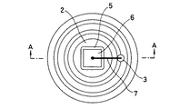
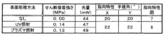
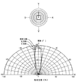
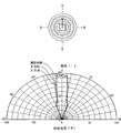
2 第一電極
3 第二電極
4 ランプハウス
5 導電性ペースト
6 LEDチップ
7 ボンディングワイヤ
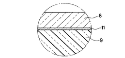
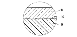
8 レンズ
9 シリコーン樹脂
10 凹凸面
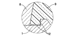
11 表面改質層11
12 隙間
13 窪み
14 非接着部
Claims (3)
- 絶縁体に複数の金属部を設けたランプハウスの少なくとも1ヶ所の金属部にLEDチップを載設し、第一の光透過性樹脂からなり開口部を有する形状のレンズを前記開口部が対向するように前記ランプハウスに取付け、該ランプハウスと前記レンズとで形成された空間に第二の光透過性樹脂を充填した半導体発光装置であって、
前記第二の光透過性樹脂は、前記第一の光透過性樹脂よりも柔軟性の高い樹脂から構成され、
前記第二の光透過性樹脂の線膨張率は、前記絶縁体および前記第一の光透過性樹脂の線膨張率より大きく、
前記レンズの前記第二の光透過性樹脂と接触する面に前記第二の光透過性樹脂との接着強度を高める表面処理が施され、前記第二の光透過性樹脂と前記絶縁体との接着強度を前記レンズと前記第二の光透過性樹脂との接着強度より低い接着強度とすることを特徴とする半導体発光装置。 - 前記絶縁体と前記第二の光透過性樹脂との間に非接着部が形成されていることを特徴とする請求項1に記載の半導体発光装置。
- 前記絶縁体の前記第二の光透過性樹脂側には窪みが設けられ、
前記非接着部は、前記窪みに形成されていることを特徴とする請求項2に記載の半導体発光装置。
Priority Applications (1)
| Application Number | Priority Date | Filing Date | Title |
|---|---|---|---|
| JP2003369568A JP4526257B2 (ja) | 2003-10-29 | 2003-10-29 | 半導体発光装置 |
Applications Claiming Priority (1)
| Application Number | Priority Date | Filing Date | Title |
|---|---|---|---|
| JP2003369568A JP4526257B2 (ja) | 2003-10-29 | 2003-10-29 | 半導体発光装置 |
Publications (2)
| Publication Number | Publication Date |
|---|---|
| JP2005136101A JP2005136101A (ja) | 2005-05-26 |
| JP4526257B2 true JP4526257B2 (ja) | 2010-08-18 |
Family
ID=34646872
Family Applications (1)
| Application Number | Title | Priority Date | Filing Date |
|---|---|---|---|
| JP2003369568A Expired - Fee Related JP4526257B2 (ja) | 2003-10-29 | 2003-10-29 | 半導体発光装置 |
Country Status (1)
| Country | Link |
|---|---|
| JP (1) | JP4526257B2 (ja) |
Families Citing this family (14)
| Publication number | Priority date | Publication date | Assignee | Title |
|---|---|---|---|---|
| KR100738251B1 (ko) * | 2005-09-05 | 2007-07-16 | 럭스피아(주) | 발광 유니트 및 이를 채용한 직하 발광형 백라이트 장치 |
| KR101161397B1 (ko) | 2005-09-30 | 2012-07-02 | 서울반도체 주식회사 | 실리콘 렌즈를 구비하는 발광소자 및 그것을 제조하는 방법 |
| JP2007201354A (ja) * | 2006-01-30 | 2007-08-09 | Matsushita Electric Ind Co Ltd | 発光モジュール |
| JP2007311445A (ja) | 2006-05-17 | 2007-11-29 | Stanley Electric Co Ltd | 半導体発光装置及びその製造方法 |
| US8044418B2 (en) | 2006-07-13 | 2011-10-25 | Cree, Inc. | Leadframe-based packages for solid state light emitting devices |
| US7960819B2 (en) * | 2006-07-13 | 2011-06-14 | Cree, Inc. | Leadframe-based packages for solid state emitting devices |
| KR100756617B1 (ko) | 2006-09-29 | 2007-09-07 | 서울반도체 주식회사 | 발광소자 |
| CN100521268C (zh) * | 2007-07-25 | 2009-07-29 | 友达光电股份有限公司 | 封装件及其制造方法 |
| KR101007062B1 (ko) * | 2008-03-21 | 2011-01-12 | 주식회사 루멘스 | 발광다이오드 리드프레임과 그 리드프레임을 이용한발광다이오드 패키지 및 그 제조방법 |
| JP5431259B2 (ja) * | 2010-06-30 | 2014-03-05 | シャープ株式会社 | 発光素子パッケージおよびその製造方法、発光素子アレイ、および表示装置 |
| JP5563440B2 (ja) * | 2010-12-24 | 2014-07-30 | 株式会社朝日ラバー | 樹脂レンズ、レンズ付led装置及びレンズ付led装置の製造方法 |
| JP5559027B2 (ja) * | 2010-12-24 | 2014-07-23 | 株式会社朝日ラバー | シリコーンレンズ、レンズ付led装置及びレンズ付led装置の製造方法 |
| KR101413596B1 (ko) | 2012-12-07 | 2014-07-02 | 주식회사 루멘스 | 발광장치 및 이를 구비하는 백라이트 유닛 |
| JP6116949B2 (ja) * | 2013-03-14 | 2017-04-19 | 新光電気工業株式会社 | 発光素子搭載用の配線基板、発光装置、発光素子搭載用の配線基板の製造方法及び発光装置の製造方法 |
Family Cites Families (4)
| Publication number | Priority date | Publication date | Assignee | Title |
|---|---|---|---|---|
| JP3618551B2 (ja) * | 1998-06-30 | 2005-02-09 | 株式会社東芝 | 光半導体モジュール |
| JP3614776B2 (ja) * | 2000-12-19 | 2005-01-26 | シャープ株式会社 | チップ部品型ledとその製造方法 |
| JP2002198570A (ja) * | 2000-12-26 | 2002-07-12 | Toyoda Gosei Co Ltd | 固体光素子 |
| JP2003204082A (ja) * | 2001-10-31 | 2003-07-18 | Sanyu Rec Co Ltd | 発光ダイオード |
-
2003
- 2003-10-29 JP JP2003369568A patent/JP4526257B2/ja not_active Expired - Fee Related
Also Published As
| Publication number | Publication date |
|---|---|
| JP2005136101A (ja) | 2005-05-26 |
Similar Documents
| Publication | Publication Date | Title |
|---|---|---|
| JP4526257B2 (ja) | 半導体発光装置 | |
| US10158050B2 (en) | Light-emitting device and method of manufacturing the same | |
| EP2264798B1 (en) | High powered light emitter packages with compact optics | |
| US9263658B2 (en) | Light-emitting device and method of manufacturing the same | |
| US7582496B2 (en) | LED package using Si substrate and fabricating method thereof | |
| WO2011125346A1 (ja) | 発光装置およびその製造方法 | |
| US20090289272A1 (en) | Light emitting device package | |
| US20120132937A1 (en) | Waterproof surface mount device package and method | |
| JP2013045888A (ja) | 発光装置及びその製造方法 | |
| JP2005079329A (ja) | 表面実装型発光ダイオード | |
| JP2003168829A (ja) | 発光装置 | |
| WO2013168802A1 (ja) | Ledモジュール | |
| TWI591103B (zh) | Semiconductor device and optical coupling device | |
| JPWO2017209149A1 (ja) | 発光装置 | |
| KR101812741B1 (ko) | 발광 다이오드 패키지 및 이의 제조방법 | |
| TWI464929B (zh) | 提昇散熱效率之光源模組及其嵌入式封裝結構 | |
| KR101192816B1 (ko) | Led 패키지 및 그 제조방법 | |
| JP6626537B2 (ja) | 半導体装置および光結合装置 | |
| KR200442383Y1 (ko) | 발광다이오드 소자의 어셈블리 구조 | |
| KR101719816B1 (ko) | 발광다이오드 어레이 | |
| KR101136392B1 (ko) | 광 패키지 및 그 제조 방법 | |
| JP6543391B2 (ja) | 半導体装置 | |
| KR101858387B1 (ko) | 발광다이오드 어레이 | |
| KR100773451B1 (ko) | 고효율 엘이디 램프 | |
| KR101168420B1 (ko) | 테이프 타입 led 패키지 및 그 제조 방법 |
Legal Events
| Date | Code | Title | Description |
|---|---|---|---|
| A621 | Written request for application examination |
Free format text: JAPANESE INTERMEDIATE CODE: A621 Effective date: 20060807 |
|
| A131 | Notification of reasons for refusal |
Free format text: JAPANESE INTERMEDIATE CODE: A131 Effective date: 20090602 |
|
| A977 | Report on retrieval |
Free format text: JAPANESE INTERMEDIATE CODE: A971007 Effective date: 20090602 |
|
| A521 | Request for written amendment filed |
Free format text: JAPANESE INTERMEDIATE CODE: A523 Effective date: 20090730 |
|
| A131 | Notification of reasons for refusal |
Free format text: JAPANESE INTERMEDIATE CODE: A131 Effective date: 20091208 |
|
| A521 | Request for written amendment filed |
Free format text: JAPANESE INTERMEDIATE CODE: A523 Effective date: 20100204 |
|
| TRDD | Decision of grant or rejection written | ||
| A01 | Written decision to grant a patent or to grant a registration (utility model) |
Free format text: JAPANESE INTERMEDIATE CODE: A01 Effective date: 20100511 |
|
| A01 | Written decision to grant a patent or to grant a registration (utility model) |
Free format text: JAPANESE INTERMEDIATE CODE: A01 |
|
| A61 | First payment of annual fees (during grant procedure) |
Free format text: JAPANESE INTERMEDIATE CODE: A61 Effective date: 20100601 |
|
| FPAY | Renewal fee payment (event date is renewal date of database) |
Free format text: PAYMENT UNTIL: 20130611 Year of fee payment: 3 |
|
| R150 | Certificate of patent or registration of utility model |
Free format text: JAPANESE INTERMEDIATE CODE: R150 Ref document number: 4526257 Country of ref document: JP Free format text: JAPANESE INTERMEDIATE CODE: R150 |
|
| R250 | Receipt of annual fees |
Free format text: JAPANESE INTERMEDIATE CODE: R250 |
|
| R250 | Receipt of annual fees |
Free format text: JAPANESE INTERMEDIATE CODE: R250 |
|
| R250 | Receipt of annual fees |
Free format text: JAPANESE INTERMEDIATE CODE: R250 |
|
| R250 | Receipt of annual fees |
Free format text: JAPANESE INTERMEDIATE CODE: R250 |
|
| R250 | Receipt of annual fees |
Free format text: JAPANESE INTERMEDIATE CODE: R250 |
|
| R250 | Receipt of annual fees |
Free format text: JAPANESE INTERMEDIATE CODE: R250 |
|
| LAPS | Cancellation because of no payment of annual fees |