JP4468898B2 - ポジティブ補償フィルムを有する垂直配向液晶表示装置 - Google Patents
ポジティブ補償フィルムを有する垂直配向液晶表示装置 Download PDFInfo
- Publication number
- JP4468898B2 JP4468898B2 JP2005518747A JP2005518747A JP4468898B2 JP 4468898 B2 JP4468898 B2 JP 4468898B2 JP 2005518747 A JP2005518747 A JP 2005518747A JP 2005518747 A JP2005518747 A JP 2005518747A JP 4468898 B2 JP4468898 B2 JP 4468898B2
- Authority
- JP
- Japan
- Prior art keywords
- vertical alignment
- retardation
- liquid crystal
- plate
- film
- Prior art date
- Legal status (The legal status is an assumption and is not a legal conclusion. Google has not performed a legal analysis and makes no representation as to the accuracy of the status listed.)
- Expired - Lifetime
Links
- 239000004973 liquid crystal related substance Substances 0.000 title claims description 66
- 238000010521 absorption reaction Methods 0.000 claims abstract description 25
- 230000003287 optical effect Effects 0.000 claims abstract description 16
- 210000004027 cell Anatomy 0.000 claims description 20
- 239000006185 dispersion Substances 0.000 claims description 18
- 210000002858 crystal cell Anatomy 0.000 claims description 12
- 239000011521 glass Substances 0.000 claims description 7
- 239000000758 substrate Substances 0.000 claims description 7
- 239000000654 additive Substances 0.000 claims description 4
- 230000000996 additive effect Effects 0.000 claims description 3
- 238000004040 coloring Methods 0.000 abstract 1
- 238000012986 modification Methods 0.000 description 7
- 230000004048 modification Effects 0.000 description 7
- 238000004088 simulation Methods 0.000 description 5
- 239000004988 Nematic liquid crystal Substances 0.000 description 2
- 238000005259 measurement Methods 0.000 description 2
- 238000000034 method Methods 0.000 description 2
- 229920002678 cellulose Polymers 0.000 description 1
- 239000001913 cellulose Substances 0.000 description 1
- 230000000052 comparative effect Effects 0.000 description 1
- 238000007796 conventional method Methods 0.000 description 1
- 230000000694 effects Effects 0.000 description 1
- 238000002474 experimental method Methods 0.000 description 1
- 239000007788 liquid Substances 0.000 description 1
- 230000001681 protective effect Effects 0.000 description 1
- ILJSQTXMGCGYMG-UHFFFAOYSA-N triacetic acid Chemical compound CC(=O)CC(=O)CC(O)=O ILJSQTXMGCGYMG-UHFFFAOYSA-N 0.000 description 1
Images


Classifications
-
- G—PHYSICS
- G02—OPTICS
- G02F—OPTICAL DEVICES OR ARRANGEMENTS FOR THE CONTROL OF LIGHT BY MODIFICATION OF THE OPTICAL PROPERTIES OF THE MEDIA OF THE ELEMENTS INVOLVED THEREIN; NON-LINEAR OPTICS; FREQUENCY-CHANGING OF LIGHT; OPTICAL LOGIC ELEMENTS; OPTICAL ANALOGUE/DIGITAL CONVERTERS
- G02F1/00—Devices or arrangements for the control of the intensity, colour, phase, polarisation or direction of light arriving from an independent light source, e.g. switching, gating or modulating; Non-linear optics
- G02F1/01—Devices or arrangements for the control of the intensity, colour, phase, polarisation or direction of light arriving from an independent light source, e.g. switching, gating or modulating; Non-linear optics for the control of the intensity, phase, polarisation or colour
- G02F1/13—Devices or arrangements for the control of the intensity, colour, phase, polarisation or direction of light arriving from an independent light source, e.g. switching, gating or modulating; Non-linear optics for the control of the intensity, phase, polarisation or colour based on liquid crystals, e.g. single liquid crystal display cells
- G02F1/133—Constructional arrangements; Operation of liquid crystal cells; Circuit arrangements
- G02F1/1333—Constructional arrangements; Manufacturing methods
- G02F1/1335—Structural association of cells with optical devices, e.g. polarisers or reflectors
- G02F1/13363—Birefringent elements, e.g. for optical compensation
- G02F1/133634—Birefringent elements, e.g. for optical compensation the refractive index Nz perpendicular to the element surface being different from in-plane refractive indices Nx and Ny, e.g. biaxial or with normal optical axis
-
- G—PHYSICS
- G02—OPTICS
- G02F—OPTICAL DEVICES OR ARRANGEMENTS FOR THE CONTROL OF LIGHT BY MODIFICATION OF THE OPTICAL PROPERTIES OF THE MEDIA OF THE ELEMENTS INVOLVED THEREIN; NON-LINEAR OPTICS; FREQUENCY-CHANGING OF LIGHT; OPTICAL LOGIC ELEMENTS; OPTICAL ANALOGUE/DIGITAL CONVERTERS
- G02F1/00—Devices or arrangements for the control of the intensity, colour, phase, polarisation or direction of light arriving from an independent light source, e.g. switching, gating or modulating; Non-linear optics
- G02F1/01—Devices or arrangements for the control of the intensity, colour, phase, polarisation or direction of light arriving from an independent light source, e.g. switching, gating or modulating; Non-linear optics for the control of the intensity, phase, polarisation or colour
- G02F1/13—Devices or arrangements for the control of the intensity, colour, phase, polarisation or direction of light arriving from an independent light source, e.g. switching, gating or modulating; Non-linear optics for the control of the intensity, phase, polarisation or colour based on liquid crystals, e.g. single liquid crystal display cells
- G02F1/133—Constructional arrangements; Operation of liquid crystal cells; Circuit arrangements
- G02F1/1333—Constructional arrangements; Manufacturing methods
- G02F1/1335—Structural association of cells with optical devices, e.g. polarisers or reflectors
-
- G—PHYSICS
- G02—OPTICS
- G02F—OPTICAL DEVICES OR ARRANGEMENTS FOR THE CONTROL OF LIGHT BY MODIFICATION OF THE OPTICAL PROPERTIES OF THE MEDIA OF THE ELEMENTS INVOLVED THEREIN; NON-LINEAR OPTICS; FREQUENCY-CHANGING OF LIGHT; OPTICAL LOGIC ELEMENTS; OPTICAL ANALOGUE/DIGITAL CONVERTERS
- G02F1/00—Devices or arrangements for the control of the intensity, colour, phase, polarisation or direction of light arriving from an independent light source, e.g. switching, gating or modulating; Non-linear optics
- G02F1/01—Devices or arrangements for the control of the intensity, colour, phase, polarisation or direction of light arriving from an independent light source, e.g. switching, gating or modulating; Non-linear optics for the control of the intensity, phase, polarisation or colour
- G02F1/13—Devices or arrangements for the control of the intensity, colour, phase, polarisation or direction of light arriving from an independent light source, e.g. switching, gating or modulating; Non-linear optics for the control of the intensity, phase, polarisation or colour based on liquid crystals, e.g. single liquid crystal display cells
- G02F1/137—Devices or arrangements for the control of the intensity, colour, phase, polarisation or direction of light arriving from an independent light source, e.g. switching, gating or modulating; Non-linear optics for the control of the intensity, phase, polarisation or colour based on liquid crystals, e.g. single liquid crystal display cells characterised by the electro-optical or magneto-optical effect, e.g. field-induced phase transition, orientation effect, guest-host interaction or dynamic scattering
- G02F1/139—Devices or arrangements for the control of the intensity, colour, phase, polarisation or direction of light arriving from an independent light source, e.g. switching, gating or modulating; Non-linear optics for the control of the intensity, phase, polarisation or colour based on liquid crystals, e.g. single liquid crystal display cells characterised by the electro-optical or magneto-optical effect, e.g. field-induced phase transition, orientation effect, guest-host interaction or dynamic scattering based on orientation effects in which the liquid crystal remains transparent
- G02F1/1393—Devices or arrangements for the control of the intensity, colour, phase, polarisation or direction of light arriving from an independent light source, e.g. switching, gating or modulating; Non-linear optics for the control of the intensity, phase, polarisation or colour based on liquid crystals, e.g. single liquid crystal display cells characterised by the electro-optical or magneto-optical effect, e.g. field-induced phase transition, orientation effect, guest-host interaction or dynamic scattering based on orientation effects in which the liquid crystal remains transparent the birefringence of the liquid crystal being electrically controlled, e.g. ECB-, DAP-, HAN-, PI-LC cells
-
- G—PHYSICS
- G02—OPTICS
- G02F—OPTICAL DEVICES OR ARRANGEMENTS FOR THE CONTROL OF LIGHT BY MODIFICATION OF THE OPTICAL PROPERTIES OF THE MEDIA OF THE ELEMENTS INVOLVED THEREIN; NON-LINEAR OPTICS; FREQUENCY-CHANGING OF LIGHT; OPTICAL LOGIC ELEMENTS; OPTICAL ANALOGUE/DIGITAL CONVERTERS
- G02F1/00—Devices or arrangements for the control of the intensity, colour, phase, polarisation or direction of light arriving from an independent light source, e.g. switching, gating or modulating; Non-linear optics
- G02F1/01—Devices or arrangements for the control of the intensity, colour, phase, polarisation or direction of light arriving from an independent light source, e.g. switching, gating or modulating; Non-linear optics for the control of the intensity, phase, polarisation or colour
- G02F1/13—Devices or arrangements for the control of the intensity, colour, phase, polarisation or direction of light arriving from an independent light source, e.g. switching, gating or modulating; Non-linear optics for the control of the intensity, phase, polarisation or colour based on liquid crystals, e.g. single liquid crystal display cells
- G02F1/133—Constructional arrangements; Operation of liquid crystal cells; Circuit arrangements
- G02F1/1333—Constructional arrangements; Manufacturing methods
- G02F1/1335—Structural association of cells with optical devices, e.g. polarisers or reflectors
- G02F1/13363—Birefringent elements, e.g. for optical compensation
- G02F1/133637—Birefringent elements, e.g. for optical compensation characterised by the wavelength dispersion
Landscapes
- Physics & Mathematics (AREA)
- Nonlinear Science (AREA)
- Chemical & Material Sciences (AREA)
- Crystallography & Structural Chemistry (AREA)
- General Physics & Mathematics (AREA)
- Optics & Photonics (AREA)
- Mathematical Physics (AREA)
- Liquid Crystal (AREA)
- Polarising Elements (AREA)
Description
内在されていた。
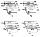
本発明の第1の実施例による垂直配向液晶表示装置は図1の(a)乃至(d)に示したように、上、下部ガラス基板の間に誘電率異方性が 負( Δε<0)、または正(Δε>0)である液晶を注入して垂直配向パネル13を形成し、前記垂直配向(VA)パネル13を中心にしてその上、下部に吸収軸が相互に直交するように2つの偏光板11、12を配置し、前記2つの偏光板と垂直配向パネルとの間にそれぞれ又はいずれかの一ヶ所に連続に第1の位相差フィルム(+A−plate)14と第2の位相差フィルム(−C−plate)15とからなるポジティブ補償フィルムが配置される形態で構成される。
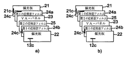
本発明の第2の実施例による垂直配向液晶表示装置は図2の(a)及び(b)に示したように、吸収軸が相互に直交する2つの偏光板21、22の間に垂直配向(VA)パネル23が配置され、前記2つの偏光板と垂直配向パネルとの間に再び2つの第1の位相差フィルム(+A−plate)24a、24bと1つの第2の位相差フィルム(−C−plate)25とからなるポジティブ補償フィルムが配置される形態であって、第1の位相差フィルムと第2の位相差フィルムとを前記垂直配向パネルと上部偏光板との間または垂直配向パネルと下部偏光板との間中のいずれか一ヶ所に連続に配置し、残りの1つの第1の位相差フィルムを前記垂直配向パネルと上部偏光板との間または垂直配向パネルと下部偏光板との間のうちの残りの一ヶ所に配置して液晶セルを構成する。
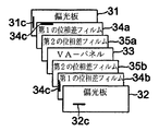
本発明の第3の実施例による垂直配向液晶表示装置は図3に示したように、吸収軸が相互に直交する2つの偏光板31、32の間に垂直配向(VA)パネル33が配置され、前記2つの偏光板と垂直配向パネルとの間にまた2つの第1の位相差フィルム(+A−plate)34a、34bと2つの第2の位相差フィルム(−C−plate)35a、35bとからなるポジティブ補償フィルムが配置される形態であって、それぞれ1つずつの第1の位相差フィルムと第2の位相差フィルムとを前記垂直配向パネルと上部偏光板との間または垂直配向パネルと下部偏光板との間中のいずれか一ヶ所に連続に配置し、残りの一ヶ所に残りの第1の位相差フィルムと第2の位相差フィルムを連続に配置して液晶セルを構成する。 図3においては、それぞれ1つずつの第1の位相差フィルム34aと第2の位相差フィルム35aとを垂直配向パネル33と下部偏光板31との間に連続に配置し、また他の第1の位相差フィルム34bと第2の位相差フィルム35bとを垂直配向パネル33と上部偏光板32との間に連続に配置した形態を例示しており、ここで前記垂直配向パネル33と下部偏光板31との間に配置された第1の位相差フィルム34aはその光軸34cが下部偏光板31の吸収軸31cに垂直に配置され、前記垂直配向パネル33と上部偏光板32との間に配置された第1の位相差フィルム34bはその光軸34cが前記上部偏光板32の吸収軸32cに垂直に配置される。
[式]
RVA、550+R−C、550=100nm〜130nm(平均115nm)
[式]
(Δnλ/Δn550)VA ×RVA、550 + (Δnλ/Δn550)−C ×R−C,550 = 115nm
(Δn400/Δn550)VA ×RVA、550 + (Δn400/Δn550)−C ×R−C,550 = 115nm
R400/R550= 400/550 = 0.727、 R700/R550= 700/550 = 1.273である。
本実験例のサンプルは第1の実施例による図1(a)のVA−LCDを使用した。3μmのセルギャップを有するVA−パネルを含んでおり、液晶分子の方向子が有するプレチルト角は89°、誘電率異方性はΔε= −4.9、屈折率異方性はΔn = 0.0979、波長分散特性がΔn400/Δn550 = 1.0979である。従って、 550nmの波長でVA−パネルの厚み方向の位相差値はRVA、550 = 297nmである。

本実験例のサンプルは第1の実施例の他の変形例の1つである図1(d)のVA−LCDを使用した。4μmのセルギャップ、プレチルト角は89°、誘電率異方性はΔε= −4.9、屈折率異方性はΔn = 0.0979、波長分散特性はΔn400/Δn550 = 1.0979である。従って、 VA−パネルの厚み方向の位相差値はRVA、550 = 396nmである。
本実験例のサンプルは第2の実施例の1つである図2(a)のVA−LCDを使用した。3μmのセルギャップを有するVA−パネルを含んでおり、プレチルト角は89°であり、誘電率異方性はΔε= −4.9、屈折率異方性はΔn = 0.0979であり、波長分散特性はΔn400/Δn550 = 1.0979である。従って、 VA−パネルの厚み方向の位相差値はRVA、550 = 297nmである。
本実験例のサンプルは第3の実施例である図3のVA−LCDを使用した。3μmのセルギャップを有するVA−パネルを含んでおり、プレチルト角は89°であり、誘電率異方性はΔε= −4.9、屈折率異方性はΔn = 0.0979であり、波長分散特性は△n400/Δn550 = 1.0979である。従って、 VA−パネルの厚み方向の位相差値はRVA、550 = 297nmである。
11c、21c、31c:下部偏光版の吸収軸
12、22、32:上部偏光板
12c、22c、32c:上部偏光版の吸収軸
13、23、33:垂直配向パネル
14、24a、24b、34a、34b:第1の位相差フィルム
14c、24c、34c:第1の位相差フィルムの光軸
15、25、35a、35b:第2の位相差フィルム43:垂直配向された液晶パネルの厚み方向の位相差値
45′:第2の位相差フィルムの位相差値45:第2の位相差フィルムの位相差値の絶対値
46:第2の位相差フィルムの厚み方向の位相差値の合計
Claims (15)
- 上、下部ガラス基板の間に誘電率異方性が 負(Δε<0)、または正(Δε>0)である液晶を注入して垂直配向パネルを形成し、前記垂直配向パネルを中心にその上、下部に吸収軸が相互に直交する上、下部偏光板を配置して3〜8μmの範囲のセルギャップを保持するマルチドメイン垂直配向モード(MVA)またはキラル添加剤を使用する垂直配向モードの液晶表示素子(VA−LCD)において、
前記垂直配向パネルと上、下部偏光板との間に面上の屈折率nx、nyと厚み方向の屈折率nzがnx>ny=nzである第1の位相差フィルム(+A−plate)、または nx=ny>nzである第2の位相差フィルム(−C−plate)の中で少なくとも1つ以上からなるポジティブ補償フィルムを配置して液晶セルを構成し、
前記第1の位相差フィルムの光軸が隣接した偏光板の吸収軸に垂直に配置され、
前記第2の位相差フィルム(−C−plate)と垂直配向パネルとを含む厚み方向の位相差値の合計R−C+RVAが正の値の位相差補償特性を有し、
前記第1の位相差フィルム(+A−plate)は可視光の範囲内で波長が増加するほど位相差値が増加する逆波長分散特性を有し、前記第2の位相差フィルム(−C−plate)と垂直配向パネルとを含む厚み方向の位相差値の合計R −C +R VA が可視光の範囲内で一定の50nm〜150nmの範囲の値を有し、
前記第2の位相差フィルム(−C−plate)の2つの波長400nm、550nmにおける相対的な位相差値R −C、400 /R −C、550 は、前記垂直配向パネルの相対的な位相差値より大きく、2つの波長550、700nmにおける相対的な位相差値R −C、700 /R −C、550 は垂直配向パネルの相対的な位相差値より小さいことを特徴とするポジティブ補償フィルムを有する垂直配向液晶表示装置。 - 前記ポジティブ補償フィルムが1つの第1の位相差フィルム(+A−plate)と1つの第2の位相差フィルム(−C−plate)とからなり、第1の位相差フィルムと第2の位相差フィルムの中いずれか1つを前記垂直配向パネルと上部偏光板との間に選択的に配置し、もう1つのフィルムを垂直配向パネルと下部偏光板との間に配置して液晶セルを構成し、または前記垂直配向パネルと上部偏光板との間或いは垂直配向パネルと下部偏光板との間中のいずれか一ヶ所に第1の位相差フィルムと第2の位相差フィルムを連続に配置して液晶セルを構成することを特徴とする請求項1に記載の垂直配向液晶表示装置。
- 前記ポジティブ補償フィルムが2つの第1の位相差フィルム(+A−plate)と1つの第2の位相差フィルム(−C−plate)とからなり、第1の位相差フィルムと第2の位相差フィルムを前記垂直配向パネルと上部偏光板との間、または垂直配向パネルと下部偏光板との間中のいずれか一ヶ所に連続に配置し、残りの1つの第1の位相差フィルムを前記垂直配向パネルと上部偏光板との間または垂直配向パネルと下部偏光板との間のうちの残りの一ヶ所に配置して液晶セルを構成することを特徴とする請求項1に記載の垂直配向液晶表示装置。
- 前記ポジティブ補償フィルムが2つの第1の位相差フィルム(+A−plate)と2つの第2の位相差フィルム(−C−plate)とからなり、第1の位相差フィルムと第2の位相差フィルムを前記垂直配向パネルと上部偏光板との間及び垂直配向パネルと下部偏光板との間にそれぞれ連続に配置して液晶セルを構成することを特徴とする請求項1に記載の垂直配向液晶表示装置。
- 電圧が印加されていない状態における前記垂直配向パネルの液晶分子の方向子は前記垂直配向パネルの上、下部ガラス基板の間で、75〜90°の範囲内のプレチルト角を有することを特徴とする請求項1に記載のポジティブ補償フィルムを有する垂直配向液晶表示装置。
- 前記プレチルト角が87〜90°であることを特徴とする請求項5に記載のポジティブ補償フィルムを有する垂直配向液晶表示装置。
- 前記プレチルト角が89〜90°であることを特徴とする請求項5に記載のポジティブ補償フィルムを有する垂直配向液晶表示装置。
- 前記垂直配向パネルに形成される液晶層の位相差値が550nmの波長で80nm〜400nmの範囲を有することを特徴とする請求項1に記載のポジティブ補償フィルムを有する垂直配向液晶表示装置。
- 前記垂直配向パネルに形成される液晶層の位相差値が550nmの波長で80nm〜300nmの範囲を有することを特徴とする請求項8に記載のポジティブ補償フィルムを有する垂直配向液晶表示装置。
- 前記垂直配向パネルに注入された液晶のラビング方向が前記偏光板の吸収軸と45°をなすことを特徴とする請求項1に記載のポジティブ補償フィルムを有する垂直配向液晶表示装置。
- 前記第1の位相差フィルム(+A−plate)が550nmの波長で20nm〜200nmの範囲の位相差値を有することを特徴とする請求項1に記載のポジティブ補償フィルムを有する垂直配向液晶表示装置。
- 前記第1の位相差フィルム(+A−plate)が550nmの波長で130nm〜160nmの範囲の位相差値を有することを特徴とする請求項11に記載のポジティブ補償フィルムを有する垂直配向液晶表示装置。
- 前記第1の位相差フィルム(+A−plate)の位相差値の比RA、400/RA、550の範囲が0.6〜0.9であり、相対的な位相差値の比 RA、700/RA、500の範囲が1.1〜1.5であることを特徴とする請求項1に記載のポジティブ補償フィルムを有する垂直配向液晶表示装置。
- 前記第2の位相差フィルム(−C−plate)が550nmの波長で−100nm〜−400nmの範囲の厚み方向の位相差値を有することを特徴とする請求項1に記載のポジティブ補償フィルムを有する垂直配向液晶表示装置。
- 前記第2の位相差フィルム(−C−plate)の2つの波長の400nm、550nmにおける厚み方向の相対的な位相差値R−C、400/R−C、550は1.1〜1.3の範囲の値を有し、2つの波長550nm、700nmにおける厚み方向の相対的な位相差値R−C、700/R−C、550は0.8〜0.9の範囲を有することを特徴とする請求項1に記載のポジティブ補償フィルムを有する垂直配向液晶表示装置。
Applications Claiming Priority (2)
| Application Number | Priority Date | Filing Date | Title |
|---|---|---|---|
| KR10-2003-0005466A KR100498267B1 (ko) | 2003-01-28 | 2003-01-28 | 포지티브 보상필름을 갖는 수직배향 액정표시장치 |
| PCT/KR2004/000131 WO2004068223A1 (en) | 2003-01-28 | 2004-01-27 | Vertically aligned liquid crystal display having positive compensation film |
Publications (2)
| Publication Number | Publication Date |
|---|---|
| JP2006515080A JP2006515080A (ja) | 2006-05-18 |
| JP4468898B2 true JP4468898B2 (ja) | 2010-05-26 |
Family
ID=36140005
Family Applications (1)
| Application Number | Title | Priority Date | Filing Date |
|---|---|---|---|
| JP2005518747A Expired - Lifetime JP4468898B2 (ja) | 2003-01-28 | 2004-01-27 | ポジティブ補償フィルムを有する垂直配向液晶表示装置 |
Country Status (8)
| Country | Link |
|---|---|
| US (1) | US7397524B2 (ja) |
| EP (1) | EP1588212B1 (ja) |
| JP (1) | JP4468898B2 (ja) |
| KR (1) | KR100498267B1 (ja) |
| CN (1) | CN100417986C (ja) |
| AT (1) | ATE421714T1 (ja) |
| DE (1) | DE602004019186D1 (ja) |
| WO (1) | WO2004068223A1 (ja) |
Families Citing this family (38)
| Publication number | Priority date | Publication date | Assignee | Title |
|---|---|---|---|---|
| KR101022560B1 (ko) * | 2003-12-30 | 2011-03-16 | 엘지디스플레이 주식회사 | 광효율 향상 필름 및 이를 이용한 액정표시장치 |
| KR100979863B1 (ko) * | 2004-06-29 | 2010-09-02 | 샤프 가부시키가이샤 | 액정 표시 장치 |
| US7450204B1 (en) * | 2004-11-02 | 2008-11-11 | University Of Central Florida Research Foundation, Inc. | Multi-film compensated liquid crystal display with initial homogeneous alignment |
| KR100682230B1 (ko) * | 2004-11-12 | 2007-02-12 | 주식회사 엘지화학 | 수직 배향 액정표시장치 |
| CN100480810C (zh) * | 2005-03-10 | 2009-04-22 | Lg化学株式会社 | 具有使用+a-膜和+c-膜的宽视角补偿膜的垂直取向液晶显示器 |
| JP4407544B2 (ja) * | 2005-03-11 | 2010-02-03 | セイコーエプソン株式会社 | 投射型表示装置 |
| JP4681334B2 (ja) * | 2005-03-31 | 2011-05-11 | 帝人株式会社 | 積層位相差フィルム |
| JP2007004123A (ja) * | 2005-05-25 | 2007-01-11 | Nitto Denko Corp | 光学フィルム、液晶パネル、および液晶表示装置 |
| JP2007017958A (ja) * | 2005-06-08 | 2007-01-25 | Fujifilm Corp | 液晶表示装置 |
| JP4318146B2 (ja) * | 2005-06-22 | 2009-08-19 | 日東電工株式会社 | 液晶パネルおよびそれを用いた液晶表示装置 |
| US7511792B2 (en) | 2005-07-29 | 2009-03-31 | Lg Chem, Ltd. | In-plane switching liquid crystal display having simple structure |
| JP2007114762A (ja) * | 2005-09-26 | 2007-05-10 | Nitto Denko Corp | 光学補償層付偏光板、光学補償層付偏光板を用いた液晶パネル、液晶表示装置、および画像表示装置 |
| US20100134737A1 (en) * | 2006-02-20 | 2010-06-03 | Nitto Denko Corporation | Liquid crystal panel, liquid crystal display apparatus using the panel, and method of producing a liquid crystal panel |
| WO2007097158A1 (ja) * | 2006-02-20 | 2007-08-30 | Nitto Denko Corporation | 液晶パネルおよびそれを用いた液晶表示装置 |
| JP4894036B2 (ja) * | 2006-05-09 | 2012-03-07 | スタンレー電気株式会社 | 液晶表示装置 |
| GB0611184D0 (en) | 2006-06-06 | 2006-07-19 | Crysoptix Ltd | Liquid crystal display operating in a vertically aligned mode |
| KR101049354B1 (ko) * | 2006-06-28 | 2011-07-13 | 샤프 가부시키가이샤 | 복합 복굴절 매체, 편광판 및 액정 표시 장치 |
| JP2009015279A (ja) * | 2006-11-27 | 2009-01-22 | Nitto Denko Corp | 液晶パネルおよび液晶表示装置 |
| JP2008209666A (ja) * | 2007-02-27 | 2008-09-11 | Nitto Denko Corp | 光学積層体の製造方法、及び画像表示装置 |
| JP2009169263A (ja) * | 2008-01-18 | 2009-07-30 | Polatechno Co Ltd | 垂直配向液晶パネル用位相差板 |
| US7948592B2 (en) * | 2008-06-23 | 2011-05-24 | Samsung Electronics Co., Ltd. | Display device for increasing viewing angle |
| KR101508543B1 (ko) * | 2008-11-24 | 2015-04-08 | 엘지디스플레이 주식회사 | 광학 보상필름을 포함하는 수직전계방식 액정표시장치 |
| KR101040643B1 (ko) * | 2008-12-31 | 2011-06-10 | 동아대학교 산학협력단 | 광시야각형 수직정렬 액정셀을 위한 광학구조 |
| KR101414103B1 (ko) * | 2009-12-08 | 2014-07-02 | 엘지디스플레이 주식회사 | 투명 액정표시소자 |
| KR101694871B1 (ko) * | 2010-07-20 | 2017-01-11 | 동우 화인켐 주식회사 | 입체화상시스템 |
| TWI453509B (zh) | 2011-12-14 | 2014-09-21 | Ind Tech Res Inst | 雙光軸相位差膜及其製造方法 |
| KR20140085316A (ko) * | 2012-12-27 | 2014-07-07 | 삼성전자주식회사 | 광학 필름 및 이를 포함하는 유기 발광 표시 장치 |
| CN103364995B (zh) * | 2013-07-10 | 2016-03-09 | 深圳市华星光电技术有限公司 | 液晶显示器及其光学补偿方法 |
| CN110058344A (zh) * | 2013-08-09 | 2019-07-26 | 住友化学株式会社 | 光学膜 |
| CN104035234B (zh) * | 2014-06-25 | 2016-06-01 | 深圳市华星光电技术有限公司 | 液晶显示器及其光学补偿方法 |
| JP2018205362A (ja) * | 2017-05-30 | 2018-12-27 | 大日本印刷株式会社 | 偏光板補償フィルム、液晶パネル |
| WO2019088269A1 (ja) * | 2017-11-02 | 2019-05-09 | 富士フイルム株式会社 | 液晶表示装置 |
| CN109212652A (zh) * | 2018-09-30 | 2019-01-15 | 惠科股份有限公司 | 偏光板及显示装置 |
| CN208721822U (zh) * | 2018-09-30 | 2019-04-09 | 惠科股份有限公司 | 偏光板、显示面板及显示装置 |
| CN109031501A (zh) * | 2018-09-30 | 2018-12-18 | 惠科股份有限公司 | 偏光结构、显示面板及显示装置 |
| CN112526754A (zh) * | 2020-12-10 | 2021-03-19 | 深圳惠牛科技有限公司 | 显示器件及头戴式显示器 |
| CN113219724A (zh) * | 2021-04-26 | 2021-08-06 | 北海惠科光电技术有限公司 | 一种液晶显示器及显示装置 |
| WO2023226014A1 (zh) * | 2022-05-27 | 2023-11-30 | 京东方科技集团股份有限公司 | 液晶显示面板和显示装置 |
Family Cites Families (13)
| Publication number | Priority date | Publication date | Assignee | Title |
|---|---|---|---|---|
| FR2595156B1 (fr) * | 1986-02-28 | 1988-04-29 | Commissariat Energie Atomique | Cellule a cristal liquide utilisant l'effet de birefringence controlee electriquement et procedes de fabrication de la cellule et d'un milieu uniaxe d'anisotropie optique negative, utilisable dans celle-ci |
| US5477358A (en) * | 1993-06-21 | 1995-12-19 | Case Western Reserve University | Chiral nematic liquid crystal display with homeotropic alignment and negative dielectric anisotropy |
| JPH0784252A (ja) * | 1993-09-16 | 1995-03-31 | Sharp Corp | 液晶表示装置 |
| US5504603A (en) * | 1994-04-04 | 1996-04-02 | Rockwell International Corporation | Optical compensator for improved gray scale performance in liquid crystal display |
| KR100339471B1 (ko) * | 1994-09-30 | 2002-12-28 | 로크웰 인터내셔널 코포레이션 | 수직 배향 콜레스테릭 액정 디스플레이의 시야각 향상 |
| JP3282986B2 (ja) | 1996-02-28 | 2002-05-20 | 富士通株式会社 | 液晶表示装置 |
| US6642981B1 (en) | 1996-09-30 | 2003-11-04 | Fujitsu Display Technologies Corporation | Liquid crystal display device operating in a vertically aligned mode including at least one retardation film |
| JP3330574B2 (ja) | 1996-09-30 | 2002-09-30 | 富士通株式会社 | 液晶表示装置 |
| CA2316828C (en) * | 1998-10-30 | 2010-02-23 | Teijin Limited | Retardation film and optical device employing it |
| EP1118885B1 (en) * | 1999-07-29 | 2004-03-03 | Teijin Limited | Phase difference film, phase difference film composite and liquid crystal display device using the same |
| JP2001042127A (ja) | 1999-08-04 | 2001-02-16 | Nitto Denko Corp | 複合位相差板、光学補償偏光板及び液晶表示装置 |
| US6867834B1 (en) * | 1999-09-16 | 2005-03-15 | Merck Patent Gmbh | Optical compensator for LCD including stacked films of only one O-plate, one A-plate and two negative C-plate retarders |
| JP3957257B2 (ja) * | 2000-09-20 | 2007-08-15 | 日東電工株式会社 | 液晶表示装置 |
-
2003
- 2003-01-28 KR KR10-2003-0005466A patent/KR100498267B1/ko not_active Expired - Lifetime
-
2004
- 2004-01-27 US US10/543,623 patent/US7397524B2/en not_active Expired - Lifetime
- 2004-01-27 JP JP2005518747A patent/JP4468898B2/ja not_active Expired - Lifetime
- 2004-01-27 AT AT04705548T patent/ATE421714T1/de not_active IP Right Cessation
- 2004-01-27 EP EP04705548A patent/EP1588212B1/en not_active Expired - Lifetime
- 2004-01-27 CN CNB2004800029860A patent/CN100417986C/zh not_active Expired - Lifetime
- 2004-01-27 DE DE602004019186T patent/DE602004019186D1/de not_active Expired - Lifetime
- 2004-01-27 WO PCT/KR2004/000131 patent/WO2004068223A1/en not_active Ceased
Also Published As
| Publication number | Publication date |
|---|---|
| EP1588212A4 (en) | 2006-04-19 |
| DE602004019186D1 (de) | 2009-03-12 |
| US20060176426A1 (en) | 2006-08-10 |
| ATE421714T1 (de) | 2009-02-15 |
| KR20040069045A (ko) | 2004-08-04 |
| WO2004068223A1 (en) | 2004-08-12 |
| JP2006515080A (ja) | 2006-05-18 |
| EP1588212B1 (en) | 2009-01-21 |
| EP1588212A1 (en) | 2005-10-26 |
| US7397524B2 (en) | 2008-07-08 |
| KR100498267B1 (ko) | 2005-06-29 |
| CN100417986C (zh) | 2008-09-10 |
| CN1745329A (zh) | 2006-03-08 |
Similar Documents
| Publication | Publication Date | Title |
|---|---|---|
| JP4468898B2 (ja) | ポジティブ補償フィルムを有する垂直配向液晶表示装置 | |
| JP4430015B2 (ja) | ネガティブ補償フィルムを有する垂直配向液晶表示装置 | |
| CN100381915C (zh) | 双轴延迟补偿膜和使用该双轴延迟补偿膜的垂直排列的液晶显示器 | |
| JP4790842B2 (ja) | 垂直配向液晶表示装置 | |
| JP4907993B2 (ja) | 負の二軸性位相差フィルムと+c−プレートを用いた視野角の補償フィルムを含むips液晶表示装置 | |
| KR100677050B1 (ko) | +a-플레이트와 +c-플레이트를 이용한 시야각보상필름을 포함하는 면상 스위칭 액정 표시장치 | |
| KR100601916B1 (ko) | 양의 이축성 위상차 필름을 이용한 시야각 보상필름을포함하는 면상 스위칭 액정 표시장치 | |
| US20090040437A1 (en) | In-plane switching liquid crystal display including viewing angle compensation film using +A-plate | |
| JP4723590B2 (ja) | +a‐フィルムと+c‐フィルムとを用いた広視野角補償フィルムを有する垂直配向の液晶表示装置 | |
| JP4536543B2 (ja) | 液晶表示装置 | |
| JP4459229B2 (ja) | 垂直配向液晶表示装置 | |
| KR20070024785A (ko) | 광시야각 특성이 개선된 액정표시장치 | |
| KR20070024784A (ko) | 광시야각 특성이 개선된 액정표시장치 | |
| KR20070024781A (ko) | 광시야각 특성이 개선된 액정표시장치 |
Legal Events
| Date | Code | Title | Description |
|---|---|---|---|
| A131 | Notification of reasons for refusal |
Free format text: JAPANESE INTERMEDIATE CODE: A131 Effective date: 20090127 |
|
| A521 | Request for written amendment filed |
Free format text: JAPANESE INTERMEDIATE CODE: A523 Effective date: 20090427 |
|
| TRDD | Decision of grant or rejection written | ||
| A01 | Written decision to grant a patent or to grant a registration (utility model) |
Free format text: JAPANESE INTERMEDIATE CODE: A01 Effective date: 20100126 |
|
| A01 | Written decision to grant a patent or to grant a registration (utility model) |
Free format text: JAPANESE INTERMEDIATE CODE: A01 |
|
| A61 | First payment of annual fees (during grant procedure) |
Free format text: JAPANESE INTERMEDIATE CODE: A61 Effective date: 20100225 |
|
| R150 | Certificate of patent or registration of utility model |
Ref document number: 4468898 Country of ref document: JP Free format text: JAPANESE INTERMEDIATE CODE: R150 |
|
| FPAY | Renewal fee payment (event date is renewal date of database) |
Free format text: PAYMENT UNTIL: 20130305 Year of fee payment: 3 |
|
| FPAY | Renewal fee payment (event date is renewal date of database) |
Free format text: PAYMENT UNTIL: 20140305 Year of fee payment: 4 |
|
| R250 | Receipt of annual fees |
Free format text: JAPANESE INTERMEDIATE CODE: R250 |
|
| R250 | Receipt of annual fees |
Free format text: JAPANESE INTERMEDIATE CODE: R250 |
|
| R250 | Receipt of annual fees |
Free format text: JAPANESE INTERMEDIATE CODE: R250 |
|
| R250 | Receipt of annual fees |
Free format text: JAPANESE INTERMEDIATE CODE: R250 |
|
| R250 | Receipt of annual fees |
Free format text: JAPANESE INTERMEDIATE CODE: R250 |
|
| R250 | Receipt of annual fees |
Free format text: JAPANESE INTERMEDIATE CODE: R250 |
|
| R250 | Receipt of annual fees |
Free format text: JAPANESE INTERMEDIATE CODE: R250 |
|
| R250 | Receipt of annual fees |
Free format text: JAPANESE INTERMEDIATE CODE: R250 |
|
| R250 | Receipt of annual fees |
Free format text: JAPANESE INTERMEDIATE CODE: R250 |
|
| R250 | Receipt of annual fees |
Free format text: JAPANESE INTERMEDIATE CODE: R250 |
|
| R250 | Receipt of annual fees |
Free format text: JAPANESE INTERMEDIATE CODE: R250 |
|
| EXPY | Cancellation because of completion of term |