JP4421365B2 - Level conversion circuit - Google Patents
Level conversion circuit Download PDFInfo
- Publication number
- JP4421365B2 JP4421365B2 JP2004125869A JP2004125869A JP4421365B2 JP 4421365 B2 JP4421365 B2 JP 4421365B2 JP 2004125869 A JP2004125869 A JP 2004125869A JP 2004125869 A JP2004125869 A JP 2004125869A JP 4421365 B2 JP4421365 B2 JP 4421365B2
- Authority
- JP
- Japan
- Prior art keywords
- circuit
- bias
- level
- voltage
- level conversion
- Prior art date
- Legal status (The legal status is an assumption and is not a legal conclusion. Google has not performed a legal analysis and makes no representation as to the accuracy of the status listed.)
- Expired - Lifetime
Links
- 238000006243 chemical reaction Methods 0.000 title claims description 298
- 238000005513 bias potential Methods 0.000 claims description 138
- 239000003990 capacitor Substances 0.000 claims description 68
- 230000000630 rising effect Effects 0.000 claims description 7
- 230000000087 stabilizing effect Effects 0.000 claims description 5
- 230000015556 catabolic process Effects 0.000 description 67
- 238000010586 diagram Methods 0.000 description 25
- 238000005070 sampling Methods 0.000 description 16
- 230000007423 decrease Effects 0.000 description 15
- 230000008859 change Effects 0.000 description 13
- 238000013461 design Methods 0.000 description 9
- 238000000034 method Methods 0.000 description 9
- 239000004065 semiconductor Substances 0.000 description 9
- 230000002829 reductive effect Effects 0.000 description 8
- 102100021102 Hyaluronidase PH-20 Human genes 0.000 description 6
- 101150055528 SPAM1 gene Proteins 0.000 description 6
- 238000012360 testing method Methods 0.000 description 6
- 102100034323 Disintegrin and metalloproteinase domain-containing protein 2 Human genes 0.000 description 5
- 101710116108 Disintegrin and metalloproteinase domain-containing protein 2 Proteins 0.000 description 5
- 230000008878 coupling Effects 0.000 description 5
- 238000010168 coupling process Methods 0.000 description 5
- 238000005859 coupling reaction Methods 0.000 description 5
- 230000000694 effects Effects 0.000 description 5
- 230000000670 limiting effect Effects 0.000 description 5
- HCUOEKSZWPGJIM-YBRHCDHNSA-N (e,2e)-2-hydroxyimino-6-methoxy-4-methyl-5-nitrohex-3-enamide Chemical compound COCC([N+]([O-])=O)\C(C)=C\C(=N/O)\C(N)=O HCUOEKSZWPGJIM-YBRHCDHNSA-N 0.000 description 4
- 101001109689 Homo sapiens Nuclear receptor subfamily 4 group A member 3 Proteins 0.000 description 4
- 101000598778 Homo sapiens Protein OSCP1 Proteins 0.000 description 4
- 101001067395 Mus musculus Phospholipid scramblase 1 Proteins 0.000 description 4
- 102100022673 Nuclear receptor subfamily 4 group A member 3 Human genes 0.000 description 4
- 230000008901 benefit Effects 0.000 description 4
- 101000597542 Homo sapiens Pyruvate dehydrogenase protein X component, mitochondrial Proteins 0.000 description 3
- 102100035459 Pyruvate dehydrogenase protein X component, mitochondrial Human genes 0.000 description 3
- 230000003111 delayed effect Effects 0.000 description 3
- 238000005516 engineering process Methods 0.000 description 3
- 238000005259 measurement Methods 0.000 description 3
- 230000002441 reversible effect Effects 0.000 description 3
- 101150110971 CIN7 gene Proteins 0.000 description 2
- 101150110298 INV1 gene Proteins 0.000 description 2
- 101100397044 Xenopus laevis invs-a gene Proteins 0.000 description 2
- 230000010354 integration Effects 0.000 description 2
- 230000003071 parasitic effect Effects 0.000 description 2
- 230000008569 process Effects 0.000 description 2
- 230000006641 stabilisation Effects 0.000 description 2
- 238000011105 stabilization Methods 0.000 description 2
- 239000000758 substrate Substances 0.000 description 2
- 230000002411 adverse Effects 0.000 description 1
- 230000003321 amplification Effects 0.000 description 1
- 238000013459 approach Methods 0.000 description 1
- 230000005540 biological transmission Effects 0.000 description 1
- 230000000295 complement effect Effects 0.000 description 1
- 230000003247 decreasing effect Effects 0.000 description 1
- 238000003199 nucleic acid amplification method Methods 0.000 description 1
- 238000012545 processing Methods 0.000 description 1
- 230000009467 reduction Effects 0.000 description 1
- 230000004044 response Effects 0.000 description 1
- 230000001052 transient effect Effects 0.000 description 1
- 230000007704 transition Effects 0.000 description 1
Images


Classifications
-
- H—ELECTRICITY
- H03—ELECTRONIC CIRCUITRY
- H03K—PULSE TECHNIQUE
- H03K3/00—Circuits for generating electric pulses; Monostable, bistable or multistable circuits
- H03K3/02—Generators characterised by the type of circuit or by the means used for producing pulses
- H03K3/353—Generators characterised by the type of circuit or by the means used for producing pulses by the use, as active elements, of field-effect transistors with internal or external positive feedback
- H03K3/356—Bistable circuits
- H03K3/356104—Bistable circuits using complementary field-effect transistors
- H03K3/356113—Bistable circuits using complementary field-effect transistors using additional transistors in the input circuit
-
- H—ELECTRICITY
- H03—ELECTRONIC CIRCUITRY
- H03K—PULSE TECHNIQUE
- H03K17/00—Electronic switching or gating, i.e. not by contact-making and –breaking
- H03K17/10—Modifications for increasing the maximum permissible switched voltage
- H03K17/102—Modifications for increasing the maximum permissible switched voltage in field-effect transistor switches
-
- H—ELECTRICITY
- H03—ELECTRONIC CIRCUITRY
- H03K—PULSE TECHNIQUE
- H03K17/00—Electronic switching or gating, i.e. not by contact-making and –breaking
- H03K17/22—Modifications for ensuring a predetermined initial state when the supply voltage has been applied
- H03K17/223—Modifications for ensuring a predetermined initial state when the supply voltage has been applied in field-effect transistor switches
Landscapes
- Logic Circuits (AREA)
- Analogue/Digital Conversion (AREA)
Description
本発明は、入力信号の電圧レベルをレベルシフトして出力するレベル変換回路に関するものである。
多電源の半導体集積回路装置(LSI)では、異なる電源電圧の回路間を接続するためにレベル変換回路が設けられている。異なる電源電圧の回路間を接続するレベル変換回路、特に、低い電源電圧の回路の信号を、高い電源電圧の回路の信号に変換するレベル変換回路(昇圧用のレベル変換回路)は、高い電源電圧の回路信号を低い電源電圧の回路信号に変換する回路(降圧用のレベル変換回路)に比較して、増幅機能が必要となることから、遅延時間、消費電力が大きくなり易い。そのため、遅延時間や消費電力を低減できるレベル変換回路が必要となっている。
The present invention relates to a level conversion circuit that shifts and outputs a voltage level of an input signal.
In a multi-power supply semiconductor integrated circuit device (LSI), a level conversion circuit is provided to connect circuits having different power supply voltages. A level conversion circuit that connects circuits of different power supply voltages, particularly a level conversion circuit (a level conversion circuit for boosting) that converts a signal of a circuit of a low power supply voltage into a signal of a circuit of a high power supply voltage has a high power supply voltage. Compared with a circuit (a step-down level conversion circuit) that converts a circuit signal of 1 into a circuit signal of a low power supply voltage, an amplification function is required, so that the delay time and power consumption tend to increase. Therefore, a level conversion circuit that can reduce delay time and power consumption is required.
近年、半導体集積回路装置では、集積回路の微細化の進展とともに、デジタル回路の集積度の向上が続いており、その微細化に伴う信頼性の向上と消費電力の低減を図るためにデジタル回路部分の電源電圧は低下してきている。例えば、0.35umの技術で製造された集積回路の電源電圧は3.3V、0.18umの技術で製造された集積回路の電源電圧は1.8V程度となっている。一方、自動車用の制御部品として利用される半導体集積回路装置などでは、従来の5Vの電源電圧をインターフェース部の電源電圧とする要求が、いまだに根強く残っている。このため、従来の電源電圧(例えば、5V)との互換性を維持したインターフェース回路を残しながら、微細化による集積度の向上の恩恵を享受するために、内部回路の電源電圧をインターフェース回路の電源電圧よりも低い電圧値とし、内部回路を微細なCMOSプロセスで形成したLSIが数多く製造されている。 In recent years, with the progress of miniaturization of integrated circuits, the degree of integration of digital circuits has continued to improve in semiconductor integrated circuit devices. In order to improve the reliability and reduce power consumption associated with the miniaturization, The power supply voltage is decreasing. For example, the power supply voltage of an integrated circuit manufactured with a 0.35 um technology is about 3.3 V, and the power supply voltage of an integrated circuit manufactured with a 0.18 um technology is about 1.8 V. On the other hand, in semiconductor integrated circuit devices and the like used as control parts for automobiles, there is still a strong demand for using the conventional 5V power supply voltage as the power supply voltage for the interface unit. For this reason, the internal circuit power supply voltage is used as the power supply of the interface circuit in order to enjoy the benefits of increased integration due to miniaturization while leaving the interface circuit compatible with the conventional power supply voltage (for example, 5 V). Many LSIs have been manufactured in which the internal circuit is formed by a fine CMOS process with a voltage value lower than the voltage.
また、LSIの外部仕様として、電源電圧が複数ある場合に限らず、DRAM、フラッシュEEPROMなどのように、内部の昇圧回路により、外部から供給される電源電圧より高い電圧を発生し、結果的に複数の異なる電源電圧を使用するLSIや、いわゆる降圧回路により、外部から供給される電源電圧より低い内部電圧を発生し、結果的に複数の異なる電源電圧を使用するLSIも多数存在する。 Further, the external specification of LSI is not limited to the case where there are a plurality of power supply voltages, but a voltage higher than the power supply voltage supplied from the outside is generated by an internal booster circuit such as DRAM, flash EEPROM, etc. There are many LSIs that use a plurality of different power supply voltages, and an LSI that uses a plurality of different power supply voltages as a result of generating an internal voltage lower than the power supply voltage supplied from the outside by a so-called step-down circuit.
これら多電源のLSIには、異なる電源電圧の回路間を接続するためにレベル変換回路が設けられている。従来のレベル変換回路としては、特許文献1〜9等に開示されている。なお、レベル変換回路は、レベルシフト回路、或いはレベルシフタ回路とも呼ばれている。
These multi-power supply LSIs are provided with a level conversion circuit for connecting circuits having different power supply voltages. Conventional level conversion circuits are disclosed in
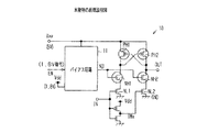
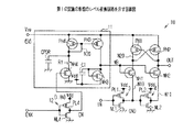
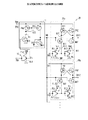
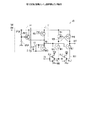
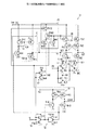
図25及び図26には、それら従来のレベル変換回路のうちの代表的な回路例を示している。なお、図25のレベル変換回路1は、特許文献1に開示されている回路であり、図26のレベル変換回路2は、特許文献2に開示されている回路である。
25 and 26 show typical circuit examples of these conventional level conversion circuits. Note that the
先ず、図25のレベル変換回路1について説明する。このレベル変換回路1は、高耐圧のPMOSトランジスタPH1,PH2、高耐圧のNMOSトランジスタNH1,NH2、低耐圧のPMOSトランジスタPL1,PL2、低耐圧のNMOSトランジスタNL1,NL2とを含む。図25において、高耐圧のMOSトランジスタについては、低耐圧のMOSトランジスタと区別するため、そのトランジスタ記号を丸で囲って図示している。なお、本明細書における他の図面においても同様に、高耐圧のMOSトランジスタの記号を丸で囲って図示している。
First, the
高耐圧のNMOSトランジスタNH1は、ドレインが高耐圧のPMOSトランジスタPH1のドレインとPMOSトランジスタPH2のゲートと接続され、ソースがグランドに接続されている。また、高耐圧のNMOSトランジスタNH2は、ドレインが高耐圧のPMOSトランジスタPH2のドレインとPMOSトランジスタPH1のゲートと接続され、ソースがグランドに接続されている。そして、各PMOSトランジスタPH1,PH2のソースには、高電圧回路部分の電源電圧Vppが供給されている。 The high breakdown voltage NMOS transistor NH1 has a drain connected to the drain of the high breakdown voltage PMOS transistor PH1 and the gate of the PMOS transistor PH2, and a source connected to the ground. The high breakdown voltage NMOS transistor NH2 has a drain connected to the drain of the high breakdown voltage PMOS transistor PH2 and the gate of the PMOS transistor PH1, and a source connected to the ground. The source voltage Vpp of the high voltage circuit portion is supplied to the sources of the PMOS transistors PH1 and PH2.
入力信号INは低耐圧のPMOSトランジスタPL1と低耐圧のNMOSトランジスタNL1とから構成されるインバータ回路3に供給される。インバータ回路3の出力ノードN10(各MOSトランジスタPL1,PL2の接続部)は、低耐圧のPMOSトランジスタPL2と低耐圧のNMOSトランジスタNL2とからなるインバータ回路4(各MOSトランジスタPL2,NL2のゲート)に接続されている。各インバータ回路3,4は、デジタル回路の電源電圧Vddが供給されて動作する。
The input signal IN is supplied to an
また、インバータ回路3の出力ノードN10は、高耐圧のNMOSトランジスタNH1のゲートに接続され、インバータ回路4の出力ノードN11は、高耐圧のNMOSトランジスタNH2のゲートに接続されている。そして、PMOSトランジスタPH2とNMOSトランジスタNH2との接続部から出力信号OUTが出力される。
The output node N10 of the
ここで、例えば、デジタル回路の電源電圧Vddが1.8Vであり、高電圧回路部分の電源電圧Vppが5Vである場合、図25のレベル変換回路1は、信号振幅が1.8Vの入力信号INを5Vの出力信号OUTにレベル変換する。
Here, for example, when the power supply voltage Vdd of the digital circuit is 1.8V and the power supply voltage Vpp of the high voltage circuit portion is 5V, the
具体的に、入力信号INがHレベル(1.8Vの電位レベル)であるとき、インバータ回路3の出力ノードN10はLレベル(0Vの電位レベル)、インバータ回路4の出力ノードN11はHレベルとなる。インバータ回路3の出力ノードN10がLレベルとなるため、NMOSトランジスタNH1はオフし、インバータ回路4の出力ノードN11がHレベルとなるため、NMOSトランジスタNH2はオンする。NMOSトランジスタNH2がオンすると、出力信号OUTはLレベルとなる。このとき、NMOSトランジスタNH2がオンし、PMOSトランジスタPH2がオフするため、回路に定常電流が流れることはない。
Specifically, when the input signal IN is at H level (1.8V potential level), the output node N10 of the
入力信号INがLレベルであるとき、インバータ回路3の出力ノードN10はHレベル、インバータ回路4の出力ノードN11はLレベルとなる。そのため、NMOSトランジスタNH1はオンし、NMOSトランジスタNH2はオフする。NMOSトランジスタNH1がオンするため、PMOSトランジスタPH1とNMOSトランジスタNH1間のノードN20はLレベルとなり、PMOSトランジスタPH2がオンする。PMOSトランジスタPH2がオンしNMOSトランジスタNH2がオフすることで、出力信号OUTはHレベルとなる。このとき、PMOSトランジスタPH2がオンし、NMOSトランジスタNH2がオフしているため、回路に定常電流が流れることはない。
When the input signal IN is at L level, the output node N10 of the
ノードN20と出力信号OUTの信号振幅は、電源電圧Vppから決まる値の5Vと大きくなり、この部分の各回路素子には電源電圧Vppの5Vが加わるため、各MOSトランジスタPH1,PH2,NH1,NH2には高耐圧のトランジスタが用いられる。一般的なMOSトランジスタでは、ゲート酸化膜を厚くすることでその耐圧が高められる。また、ゲート酸化膜を厚くするのに伴う短チャネル効果の抑制とドレイン耐圧の向上とを図るためには、長いチャネル長を確保する必要がある。 The signal amplitude of the node N20 and the output signal OUT is as large as 5V determined by the power supply voltage Vpp. Since 5V of the power supply voltage Vpp is applied to each circuit element in this portion, each MOS transistor PH1, PH2, NH1, NH2 A high breakdown voltage transistor is used for this. In a general MOS transistor, the breakdown voltage is increased by increasing the thickness of the gate oxide film. Further, in order to suppress the short channel effect and increase the drain breakdown voltage associated with increasing the thickness of the gate oxide film, it is necessary to ensure a long channel length.
このように構成した従来のレベル変換回路1は、簡単な回路構成で、かつ定常電流が流れないので広く実用化されている。
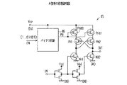
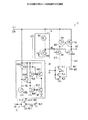
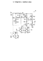
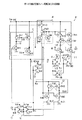
次に、図26のレベル変換回路2について説明する。なお、同図において、図25のレベル変換回路1と同一構成部分は同一符号を付している。すなわち、レベル変換回路2は、各MOSトランジスタPH1,PH2,NH1,NH2,PL1,PL2,NL1,NL2に加えて、バイアス回路6を備え、そのバイアス回路6で発生されたバイアス電位NBが高耐圧のNMOSトランジスタNH1,NH2のゲートに供給される。また、高耐圧のNMOSトランジスタNH1のソースがインバータ回路3の出力ノードN10に接続され、高耐圧のNMOSトランジスタNH2のソースがインバータ回路4の出力ノードN11に接続される。
The conventional
Next, the
バイアス回路6は、抵抗R2と高耐圧のPMOSトランジスタPH5とを含む。PMOSトランジスタPH5のソースには、抵抗R2を介して高電圧回路部分の電源電圧Vppが供給される。また、そのPMOSトランジスタPH5のゲートにはデジタル回路の電源電圧Vddが供給され、PMOSトランジスタPH5のドレインはグランドに接続されている。 The bias circuit 6 includes a resistor R2 and a high breakdown voltage PMOS transistor PH5. The power supply voltage Vpp of the high voltage circuit portion is supplied to the source of the PMOS transistor PH5 via the resistor R2. The power supply voltage Vdd of the digital circuit is supplied to the gate of the PMOS transistor PH5, and the drain of the PMOS transistor PH5 is connected to the ground.
このレベル変換回路2においても、デジタル回路の電源電圧Vddが1.8であり、高電圧回路部分の電源電圧Vppが5Vである場合、信号振幅が1.8Vの入力信号INを5Vの出力信号OUTにレベル変換する。また、バイアス回路6におけるバイアス電位NBは、電源電圧Vddに対してPMOSトランジスタPH5のしきい値電圧Vth程度高い電位(Vdd+Vth)となる。バイアス回路6の抵抗R2は、ソースホロワ回路の電流源として機能する。
Also in this
具体的に、入力信号INがHレベル(1.8V)である場合、インバータ回路3の出力ノードN10はLレベル(0V)、インバータ回路4の出力ノードN11はHレベル(1.8V)となる。ここで、バイアス回路6のバイアス電位NBを、電源電圧Vddからしきい値電圧(例えば、0.6V)だけ高い2.4V(=1.8V+0.6V)の電位とする。この場合、ノードN10がLレベル(0V)、バイアス電位NBが2.4Vであるため、NMOSトランジスタNH1はオン状態(導通状態)となる。また、ノードN11がHレベル(1.8V)、バイアス電位NBが2.4Vであるため、NMOSトランジスタNH2のゲート・ソース間には、0.6Vの電圧しか加わらない。そのため、NMOSトランジスタNH2はオフ状態(非導通状態)となる。
Specifically, when the input signal IN is at the H level (1.8V), the output node N10 of the
このとき、NMOSトランジスタNH1がオンすることにより、ノードN20はLレベルとなり、PMOSトランジスタPH2がオンする。PMOSトランジスタPH2がオンし、NMOSトランジスタNH2がオフすることで、出力信号OUTはHレベルとなる。またこのとき、PMOSトランジスタPH2がオンし、NMOSトランジスタNH2がオフするため、回路に定常電流が流れることはない。 At this time, when the NMOS transistor NH1 is turned on, the node N20 becomes L level and the PMOS transistor PH2 is turned on. When the PMOS transistor PH2 is turned on and the NMOS transistor NH2 is turned off, the output signal OUT becomes H level. At this time, since the PMOS transistor PH2 is turned on and the NMOS transistor NH2 is turned off, no steady current flows in the circuit.
入力信号INがLレベルであるとき、インバータ回路3の出力ノードN10はHレベル、インバータ回路4の出力ノードN11はLレベルとなる。この場合、ノードN10がHレベル(1.8V)、バイアス電位NBが2.4Vであるため、NMOSトランジスタNH1のゲート・ソース間には、0.6Vの電圧しか加わらない。そのため、NMOSトランジスタNH1はオフ状態となる。また、ノードN11がLレベル(0V)、バイアス電位NBが2.4Vであるため、NMOSトランジスタNH2はオン状態となる。従って、出力信号OUTはLレベルとなる。またこのとき、PMOSトランジスタPH1がオンし、NMOSトランジスタNH1がオフすることでノードN20がHレベル(5V)となる。ノードN20がHレベルとなることで、PMOSトランジスタPH2がオフするため、回路に定常電流が流れることはない。
When the input signal IN is at L level, the output node N10 of the
このレベル変換回路2において、ノードN10,N20の信号振幅は0V〜1.8Vに制限されているので、低耐圧の各MOSトランジスタPL1,PL2,NL1,NL2にはデジタル回路の電源電圧Vdd以上の電圧が加わることはない。また、バイアス電位を、電源電圧Vddからしきい値電圧Vth程度高い電位(2.4V)とすることで、NMOSトランジスタNH1,NH2がオンするときのゲート・ソース間電圧が、電源電圧Vddにしきい値電圧Vthを加算した電圧値に高められ、回路の高速動作が達成される。
In this
このように、レベル変換回路2では、図1のレベル変換回路1に対してバイアス回路6を追加し、回路接続を工夫することで、バイアスの信頼性を確保しながら、高速かつ、定常電流の流れない構成を実現している。
ところで、図25のレベル変換回路1では、簡単な回路構成で低い電源電圧Vddの入力信号INを高い電源電圧Vppの出力信号OUTに変換するレベル変換機能を実現することができるが、占有面積が大きくなるといった問題がある。また、低い電源電圧Vddの電圧値が高耐圧のNMOSトランジスタNH1,NH2のしきい値電圧Vth程度まで小さくなってしまうと、遅延時間が大きくなり回路の動作速度の低下が問題となる。なお、占有面積が大きくなるといった問題については特許文献3でも指摘されている。
By the way, in the
図25のレベル変換回路1において、例えば、出力信号OUTをHレベルからLレベルに変化させる場合を考える。出力信号OUTがHレベル(5V)であるとき、それと相補的な信号レベルのノードN20はLレベル(0V)となり、入力信号INもLレベルとなっている。そして、入力信号INがHレベル(1.8V)に変化すると、ノードN10はLレベル、ノードN11はHレベルとなる。このとき、出力信号OUTがHレベルからLレベルに変化するためには、PMOSトランジスタPH2から供給される電流よりも大きな電流をNMOSトランジスタNH2が流すことで、出力端子の電位をHレベルからLレベルに放電する必要がある。ここで、PMOSトランジスタPH2のゲート・ソース間電圧には5Vが加わるのに対して、NMOSトランジスタNH2のゲート・ソース間電圧は1.8Vしかなく、PMOSトランジスタPH2の駆動電流よりもNMOSトランジスタNH2の駆動電流を大きくするためには、該トランジスタNH2のゲート幅を大きく設計しなければならない。
In the
また、低い電源電圧Vddの下限値が1.2Vである場合に、NMOSトランジスタNH2のしきい値電圧Vthの最大値が1.2Vであると仮定すると、該トランジスタNH2のゲート幅をどれだけ大きく設計したとしても、PMOSトランジスタPH2よりもNMOSトランジスタNH2の駆動電流を大きくすることが不可能となり、正常な回路動作が実現できなくなる。 Further, assuming that the maximum value of the threshold voltage Vth of the NMOS transistor NH2 is 1.2V when the lower limit value of the low power supply voltage Vdd is 1.2V, how large the gate width of the transistor NH2 is. Even if designed, it becomes impossible to increase the drive current of the NMOS transistor NH2 more than the PMOS transistor PH2, and normal circuit operation cannot be realized.
一方、図26のレベル変換回路2では、バイアス回路6を追加して回路接続を変更するといった比較的簡単な構成で、上記の欠点が解消される。このレベル変換回路2と同様の回路構成が特許文献3や特許文献4にも開示されている。
On the other hand, in the
図25のレベル変換回路1では、高耐圧のNMOSトランジスタNH1,NH2のゲートに、低い電源電圧Vddの信号を供給していた。これに対し、図26のレベル変換回路2では、NMOSトランジスタNH1,NH2のソースに電源電圧Vddの信号を供給し、NMOSトランジスタNH1,NH2のゲートには、電源電圧VddよりもNMOSトランジスタのしきい値電圧Vth程度高いバイアス電位NB(=Vdd+Vth)を供給するよう構成した。これにより、レベル変換回路2において定常電流はほとんど流れることはなく、レベル変換機能が実現され、さらに、NMOSトランジスタNH1,NH2のゲート・ソース間電圧が、電源電圧Vddよりもしきい値電圧Vth程度高い電圧となるため、回路動作の高速化が可能となる。また、このレベル変換回路2では、NMOSトランジスタNH1,NH2のゲート・ソース間電圧が高くなるので、PMOSトランジスタPH2の駆動電流よりNMOSトランジスタNH2の駆動電流を大きく設計することが容易となる。
In the
しかしながら、図26のレベル変換回路2においては、バイアス電位を発生するバイアス回路6は常に動作しており、レベル変換が必要でないときにも電流が消費されてしまう。例えば、LSIを製造し製品出荷する際には、そのLSIが所望の特性を満たしているか確認するための試験が行われる。この試験には、IDDQといわれる重要な項目がある。このIDDQとは、静止電流(Quiescent Power Supply Current)の測定項目である。CMOS回路の場合、信号が変化する瞬間のみ電流が流れ、信号変化がない定常時ではほとんど電流は流れない。リーク故障や信号固定故障があるLSIではリーク電流やCMOS回路内を流れる貫通電流によって、静止電流が増加するためそれを検出することにより故障の有無が判定される。従って、バイアス回路6における定常電流を停止できないと、LSIとしての重要な項目であるIDDQ測定の精度が低下してしまう。
However, in the
また例えば、0.18umの技術で製造された集積回路であり、1.8V、3.3V、5Vの電源電圧の各回路が混在するLSIでは、デジタル回路の電源電圧が1.8V、外部インターフェース回路の大部分の電源電圧が3.3V、一部のアナログ回路の電源電圧だけが5Vといった回路構成が考えられる。このLSIでは、1.8Vの電源電圧で動作する回路と5Vの電源電圧で動作する回路とにおいて信号レベルを変換するためのレベル変換回路が必要となるが、電源電圧が5Vである回路は全体のごく一部で、かつ動作している期間も限られるような場合がある。 Further, for example, in an integrated circuit manufactured with a 0.18 um technology, in which each circuit of 1.8 V, 3.3 V, and 5 V power supply voltage is mixed, the power supply voltage of the digital circuit is 1.8 V, and the external interface A circuit configuration in which most of the power supply voltage of the circuit is 3.3V and only some of the power supply voltages of the analog circuits is 5V is conceivable. This LSI requires a level conversion circuit for converting the signal level between a circuit that operates with a power supply voltage of 1.8V and a circuit that operates with a power supply voltage of 5V. In some cases, the period of operation is limited to a small part.
このような場合、使用する期間だけ回路を活性化して動作させ、回路を使用していない期間には電流を最小限に抑えることが望ましい。しかし、図26のレベル変換回路2では、バイアス回路6を停止させるといった回路構成の検討がなされていないため、上記のように、無駄な電流を消費するといった問題がある。
In such a case, it is desirable to activate and operate the circuit only during the period of use, and to minimize the current during the period of not using the circuit. However, in the
特許文献3のレベル変換回路も同様に、低い電源電圧の回路信号を高耐圧のNMOSトランジスタのソースに供給し、そのNMOSトランジスタのゲート電位を低い電源電圧からNMOSトランジスタのしきい値電圧程度高い電圧値にバイアスすることで、高速動作を実現している。しかし、バイアス回路の具体的な回路構成は開示されておらず、勿論、試験時などでバイアス回路を停止するといった回路も示されていない。
Similarly, the level conversion circuit of
これに対し、特許文献4のレベル変換回路では、制御信号によりバイアス電位の発生を停止するバイアス回路が開示されている。このレベル変換回路において、低い電源電圧を1.8V、高い電源電圧を5Vとする場合、バイアス回路の停止を制御するために、制御信号は5Vの信号振幅となっている。これは、低い電源電圧よりも高いバイアス電位を発生するために5V耐圧のMOSトランジスタでバイアス回路を構成する必要があるためである。
On the other hand, the level conversion circuit of
上述したように、多電源のLSIにおいて、デジタル回路の電源電圧が1.8V、外部インターフェース回路の大部分の電源電圧が3.3V、一部のアナログ回路の電源電圧が5Vといった回路構成の場合、アナログ回路は全体のごく一部でそのアナログ回路が動作している期間が限られるものも実用化されている。このLSIでは、電源電圧が5Vである各回路を使用する期間だけ活性化させて動作させ、使用しない期間は、その回路の消費電流を必要最小限に抑えることが望ましい。この場合には、1.8Vから5Vの信号にレベル変換するレベル変換回路も、バイアス回路を含めて、信号が変化しない待機時には、電流を最小限に削減することが望ましい。 As described above, in the case of a circuit configuration in which a power supply voltage of a digital circuit is 1.8 V, a power supply voltage of most external interface circuits is 3.3 V, and a power supply voltage of some analog circuits is 5 V in a multi-power supply LSI. An analog circuit that has a limited period during which the analog circuit is operating has also been put into practical use. In this LSI, it is desirable to activate and operate each circuit having a power supply voltage of 5 V only during the period of use, and to minimize the current consumption of the circuit during the period of nonuse. In this case, it is desirable that the level conversion circuit for converting the level of the signal from 1.8 V to 5 V includes the bias circuit and reduces the current to the minimum at the standby time when the signal does not change.
具体的には、電源電圧が5Vであるアナログ回路を使用する前に、レベル変換回路のバイアス回路を活性化させバイアス電位を安定化させ、その後、アナログ回路での信号処理が終了した時点でバイアス回路の電流を最小の状態とすればよい。しかし、デジタル回路は、1.8Vで動作する回路ブロックで構成するのが一般的なので、その状態の遷移を示す信号は、1.8Vの信号である。例えば、デジタル回路としてのMPUが1.8Vで動作する回路ブロックで構成され、アナログ回路としてのAD変換回路が5Vで動作する回路である場合、MCUはプログラムを実行することにより、ある時点でAD変換回路を使用することが分かる。従って、その時点でレベル変換回路のバイアス回路の電流を大きくするための制御が必要となるが、MPUから出力される制御信号は1.8Vの信号レベルであるため、その1.8Vの制御信号でバイアス回路を安定的に制御できなければならない。 Specifically, before using an analog circuit with a power supply voltage of 5 V, the bias circuit of the level conversion circuit is activated to stabilize the bias potential, and then the bias is applied when signal processing in the analog circuit is completed. The circuit current may be minimized. However, since a digital circuit is generally configured by a circuit block that operates at 1.8 V, a signal indicating the transition of the state is a 1.8 V signal. For example, when the MPU as a digital circuit is configured by a circuit block that operates at 1.8 V, and the AD conversion circuit as an analog circuit is a circuit that operates at 5 V, the MCU executes AD at a certain point in time by executing a program. It can be seen that a conversion circuit is used. Therefore, control is required to increase the current of the bias circuit of the level conversion circuit at that time, but since the control signal output from the MPU has a signal level of 1.8V, the control signal of 1.8V It must be possible to control the bias circuit stably.
特許文献4のバイアス回路のように、制御信号が5Vである場合、1.8Vの信号を5Vに変換する必要が生じ、そのためには、レベル変換回路のバイアス回路が動作していることが必要となり、1.8Vで動作する回路からバイアス回路を制御しようとすると矛盾が生じる。よって、上記のようなLSIでは、安定した制御ができる保証を得ることができなかった。
When the control signal is 5V as in the bias circuit of
特許文献4のバイアス回路において、試験時などで外部から専用の制御端子を介して5Vの制御信号を入力し、IDDQ測定時にバイアス回路の電流を停止することは可能であるが、実際の使用状態でバイアス回路の電流を停止させるための回路構成は開示されていない。また、実使用状態では、電源電圧は時間とともに変動するためバイアス回路のバイアス電位もその変動に追従できなければならない。さらに、レベル変換回路におけるMOSトランジスタのゲート・ソースのカップリング容量によってもバイアス電位が変動する。そのため、レベル変換回路の入出力信号が頻繁に変化する実使用状態では、バイアス回路にある程度電流を流してインピーダンスを下げておくことが望ましい。従って、1.8Vの制御信号でバイアス回路をオン・オフ制御、或いは電流値を制御できないと、常に最大の電流をバイアス回路に流すこととなるため、電流の消費が問題になる。
In the bias circuit of
本発明は上記問題点を解決するためになされたものであって、その目的は、電源電圧の低下に伴う動作速度の低下を防止でき、レベル変換を適切に行うことができるレベル変換回路を提供することにある。 The present invention has been made to solve the above-described problems, and an object of the present invention is to provide a level conversion circuit that can prevent a decrease in operating speed due to a decrease in power supply voltage and can perform level conversion appropriately. There is to do.
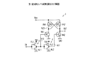
図1は、本発明の原理説明図である。すなわち、レベル変換回路10は、第1及び第2のPMOSトランジスタPH1,PH2と、第1〜第4のNMOSトランジスタNH1,NH2,NL1,NL2と、バイアス回路11とを含み、基準電圧GNDと第1電源電圧Vddを信号レベルとする入力信号INを、基準電圧GNDと第1電源電圧Vddよりも高い第2電源電圧Vppを信号レベルとする出力信号OUTにレベル変換する。このレベル変換回路10において、第1のNMOSトランジスタNH1は、ドレインが第1のPMOSトランジスタPH1のドレインと第2のPMOSトランジスタPH2のゲートに接続され、ソースが第3のNMOSトランジスタNL1のドレインに接続される。また、第2のNMOSトランジスタNH2は、ドレインが第2のPMOSトランジスタPH2のドレインと第1のPMOSトランジスタPH1のゲートに接続され、ソースが第4のNMOSトランジスタNL2のドレインに接続される。さらに、第3のNMOSトランジスタNL1のゲートに入力信号INが供給されるとともに、第4のNMOSトランジスタNL2のゲートに入力信号INを反転した信号INXが供給される。バイアス回路11は、第1電圧VddからNMOSトランジスタNH1,NH2のしきい値電圧高いバイアス電位NBを各NMOSトランジスタNH1,NH2のゲートに供給する。これにより、第1電圧VddがNMOSトランジスタのしきい値電圧の値まで小さくなったとしても、回路を高速に動作させることができる。また、第2電圧Vpp(例えば、5V)よりも低い第1電圧Vdd(例えば、1.8V)の制御信号ENに基づいて、バイアス回路11のバイアス電流が制御される。これにより、レベル変換回路10の入出力信号が頻繁に変化するときだけ、バイアス電位NBのインピーダンスを下げる等の制御を低電圧の回路(第1電圧Vddで動作する回路)側から行うことができる。
また、図3に示すレベル変換回路43では、パワーオンリセット回路44が設けられている。図4に示すように、パワーオンリセット回路44は、第2電圧Vppの立ち上がりを検出してリセット信号PORをバイアス回路11に供給し、バイアス回路11に流れるバイアス電流を増加させ、バイアス電位NBの充電を早める。これにより、電圧Vppの電源立ち上げ時に、レベル変換回路43の出力信号OUTが不定となる期間を最小にできる。
FIG. 1 is an explanatory diagram of the principle of the present invention. That is, the
In the
また、図2に示すレベル変換回路45は、第1〜第4のPMOSトランジスタPH1,PH2,PH40,PH41と、第1及び第2のNMOSトランジスタNH1,NH2と、バイアス回路46とを含み、基準電圧GNDと第1電源電圧Vddを信号レベルとする入力信号INを、基準電圧GNDと第1電源電圧Vddよりも高い第2電源電圧Vppを信号レベルとする出力信号OUTにレベル変換する。このレベル変換回路45において、第1のNMOSトランジスタNH1のドレインは、第1のPMOSトランジスタPH1のドレインと第2のPMOSトランジスタPH2のゲートに接続されている。また、第2のNMOSトランジスタNH2のドレインは、第2のPMOSトランジスタPH2のドレインと第1のPMOSトランジスタPH1のゲートに接続されている。さらに、第3のPMOSトランジスタPH40のドレインは、第1のPMOSトランジスタPH1のソースに接続され、第4のPMOSトランジスタPH41のドレインは、第2のPMOSトランジスタPH2のソースに接続されている。そして、バイアス回路46により、第3及び第4のPMOSトランジスタPH40,PH41のゲートにバイアス電位PBが供給され、出力信号OUTの変化時に第3及び第4のPMOSトランジスタPH40,PH41に流れる電流が第1及び第2のNMOSトランジスタNH1,NH2に流れる電流と比例関係となるよう制御される。このように、クロスカップルしたPMOSトランジスタPH1,PH2と直列に、電流制限のためのPMOSトランジスタPH40,PH41を設けたので、例えば、出力信号OUTをHレベルからLレベルに変化させるのに必要な条件を確実に満足するよう設計できる。つまり、従来技術のようにNMOSトランジスタNH2のゲート幅Wを大きくすることなく、PMOSトランジスタPH2の電流よりNMOSトランジスタNH2の電流を大きく設定するという条件を満足させることが可能となる。
Also, shown to the
また、図1のレベル変換回路10において、バイアス回路11は、バイアス電流を設定するための抵抗と、制御信号に基づいて抵抗に流れる電流を制御するMOSトランジスタとを備える。これによれば、制御信号に基づいてMOSトランジスタをオン/オフ制御することで、バイアス回路にバイアス電流を流したり停止したりすることができる。
In the
このレベル変換回路において、バイアス回路は、バイアス電流を設定するための抵抗を複数備えるので、動作時のバイアス電流に加え、待機時のバイアス電流を適切に設計することが可能となる。 In this level conversion circuit, since the bias circuit includes a plurality of resistors for setting the bias current, it is possible to appropriately design the standby bias current in addition to the bias current during operation.
図2のバイアス回路46において、バイアス電流の停止時には、スイッチング用のMOSトランジスタによってバイアス電位PBが基準電圧GNDの電位レベルとされる。この場合、そのバイアス電位PBに基づいて第3及び第4のPMOSトランジスタPH40,PH41がオンされるので、バイアス電流が停止される待機時に出力信号OUTが不定となるといったことを防止できる。
In the
このレベル変換回路において、バイアス電位の安定化するための容量を備えるので、電位変動が少ない正確なバイアス電位を供給することができる。 Since this level conversion circuit has a capacitor for stabilizing the bias potential, an accurate bias potential with little potential fluctuation can be supplied.
本発明によれば、動作速度の低下を防止でき、レベル変換を適切に行うことができるレベル変換回路を提供することができる。 According to the present invention, it is possible to provide a level conversion circuit that can prevent a decrease in operating speed and can appropriately perform level conversion.
(第1の実施の形態)
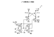
以下、本発明を具体化した第1の実施の形態を説明する。
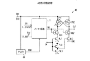
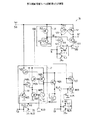
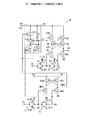
図5には、本実施の形態のレベル変換回路10を示している。このレベル変換回路10は、バイアス電位NBを発生するバイアス回路11の構成が図26に示す従来例と相違する。なお、図5において、図26の従来例と同様の構成(各MOSトランジスタPH1,PH2,NH1,NH2やインバータ回路3,4など)については同一の符号を付している。
(First embodiment)
A first embodiment embodying the present invention will be described below.
FIG. 5 shows the
このレベル変換回路10は、基準電圧の0Vと電源電圧Vddの1.8Vとを信号レベルとする入力信号INを、基準電圧の0Vと電源電圧Vppの5Vとを信号レベルとする出力信号OUTにレベル変換する。また、バイアス回路11は、デジタル回路の電源電圧Vdd(例えば、1.8V)から高耐圧のNMOSトランジスタのしきい値電圧Vth程度高いバイアス電位NB(=Vdd+Vth)を発生し、該バイアス電位NBをNMOSトランジスタNH1,NH2のゲートに供給している。
This
このバイアス回路11がVdd+Vthのバイアス電位NBを発生しているときのレベル変換回路10の動作を説明する。なおここでは、しきい値電圧Vthを0.8Vとし、バイアス電位NBを2.6V(=1.8V+0.8V)とする。
The operation of the
入力信号INがHレベル(1.8V)である場合、インバータ回路3の出力ノードN10はLレベル(0V)、バイアス電位NBは2.6Vであるので、NMOSトランジスタNH1はオンする。一方、インバータ回路4の出力ノードN11はHレベル(1.8V)、バイアス電位NBが2.6Vであるので、NMOSトランジスタNH2のゲート・ソース間には0.8Vの電圧しか加わらない。従って、NMOSトランジスタNH2は、ゲート・ソース間電圧が0.8Vであり、しきい値電圧Vthが0.8Vであるのでオフする。
When the input signal IN is at the H level (1.8V), the output node N10 of the
NMOSトランジスタNH1がオンすると、ノードN20(PMOSトランジスタPH1とNMOSトランジスタNH1の接続部)はLレベル(0V)となり、PMOSトランジスタPH2がオンする。PMOSトランジスタPH2がオンし、NMOSトランジスタNH2がオフすることで、出力信号OUTはHレベル(5V)となる。また、PMOSトランジスタPH2がオン、NMOSトランジスタNH2がオフしているので、この部分の回路に定常電流は流れない。 When the NMOS transistor NH1 is turned on, the node N20 (connection portion between the PMOS transistor PH1 and the NMOS transistor NH1) becomes L level (0 V), and the PMOS transistor PH2 is turned on. When the PMOS transistor PH2 is turned on and the NMOS transistor NH2 is turned off, the output signal OUT becomes H level (5 V). Further, since the PMOS transistor PH2 is on and the NMOS transistor NH2 is off, no steady current flows in this part of the circuit.
入力信号INがLレベルである場合、インバータ回路3の出力ノードN10はHレベル、インバータ回路4の出力ノードN11はLレベルとなる。インバータ回路3の出力ノードN10はHレベル(1.8V)、バイアス電位NBが2.6Vであり、NMOSトランジスタNH1のゲート・ソース間には0.8Vの電圧しか加わらないので、NMOSトランジスタNH1はオフする。一方、インバータ回路4の出力ノードN11はLレベル(0V)、バイアス電位NBは2.6Vであるので、NMOSトランジスタNH2はオンする。
When the input signal IN is at L level, the output node N10 of the
NMOSトランジスタNH2がオンすると、出力信号OUTはLレベル(0V)となり、PMOSトランジスタPH1はオンする。PMOSトランジスタPH1はオン、NMOSトランジスタNH1がオフすることで、ノードN20はHレベル(5V)となる。ノードN20がHレベルとなるとPMOSトランジスタPH2はオフするので、この部分の回路に定常電流は流れない。 When the NMOS transistor NH2 is turned on, the output signal OUT becomes L level (0 V), and the PMOS transistor PH1 is turned on. When the PMOS transistor PH1 is turned on and the NMOS transistor NH1 is turned off, the node N20 becomes H level (5 V). Since the PMOS transistor PH2 is turned off when the node N20 becomes H level, no steady current flows through this portion of the circuit.
各ノードN10,N11における信号振幅は0V〜1.8Vに制限されているので、耐圧が低いMOSトランジスタPL1,PL2,NL1,NL2には、デジタル部分の電源電圧vdd(=1.8V)以上の電圧が加わることがない。また、バイアス回路11で発生するバイアス電位NBを、電源電圧Vddよりもしきい値電圧Vth程度高い電圧(2.6V)とすることで、レベル変換回路10の高速動作が達成される。
Since the signal amplitude at each of the nodes N10 and N11 is limited to 0V to 1.8V, the MOS transistors PL1, PL2, NL1 and NL2 having a low withstand voltage have a power voltage vdd (= 1.8V) or more in the digital portion. No voltage is applied. Further, by setting the bias potential NB generated in the
次に、本実施の形態におけるバイアス回路11の構成について詳細に説明する。
バイアス回路11は、高耐圧のPMOSトランジスタPH3,PH4、高耐圧のNMOSトランジスタNH3,NH4、抵抗R1、及び容量C1,CPORを含む。バイアス回路11において、高耐圧のPMOSトランジスタPH3,PH4のソースには電源電圧Vpp(例えば、5V)が供給されている。また、PMOSトランジスタPH3のゲートとPMOSトランジスタPH4のゲートとが互いに接続されるとともに、各ゲートはPMOSトランジスタPH4のドレインに接続されている。つまり、各PMOSトランジスタPH3,PH4はカレントミラー回路を構成している。
Next, the configuration of the
The
PMOSトランジスタPH4のドレインは、抵抗R1を介してNMOSトランジスタNH4のドレインに接続されるとともに、容量CPORを介してグランドに接続されている。また、NMOSトランジスタNH4のソースはグランドに接続され、そのゲートには、インバータ回路12を介してイネーブル制御信号ENが供給される。このインバータ回路12は、低耐圧のPMOSトランジスタPL4とNMOSトランジスタNL4からなるCMOSインバータ回路であって、1.8Vの電源電圧Vddが供給されて動作し、制御信号ENXを反転した制御信号ENを出力する。
The drain of the PMOS transistor PH4 is connected to the drain of the NMOS transistor NH4 through the resistor R1, and is connected to the ground through the capacitor CPOR. The source of the NMOS transistor NH4 is connected to the ground, and the enable control signal EN is supplied to its gate via the
また、バイアス回路11において、高耐圧のPMOSトランジスタPH3には高耐圧のNMOSトランジスタNH3が直列に接続されており、NMOSトランジスタNH3のソースに1.8Vの電源電圧Vddが供給される。NMOSトランジスタNH3のゲートは、該NMOSトランジスタNH3のドレインに接続される。つまり、NMOSトランジスタNH3はダイオード接続されている。このダイオード接続されたNMOSトランジスタNH3と並列に容量C1が接続されている。そして、各MOSトランジスタPH3,NH3のドレインの接続部に発生されたバイアス電位NBがNMOSトランジスタNH1,NH2に供給される。
In the
このように構成したバイアス回路11の動作を説明する。
制御信号ENXがLレベル(0V)であり、そのレベルを反転したHレベル(1.8V)の制御信号ENがバイアス回路11に供給されると、NMOSトランジスタNH4がオンする。このとき、抵抗R1に電流が流れ、その電流はPMOSトランジスタPH4に流れる。すると、PMOSトランジスタPH4とカレントミラー接続されたPMOSトランジスタPH3にも電流が流れ、その電流は、ダイオード接続されたNMOSトランジスタNH3を介して低い電源電圧Vdd(デジタル回路)の電源側に流れ込む。これにより、バイアス回路11のバイアス電位NBは、電源電圧Vddから高耐圧のNMOSトランジスタNH3のしきい値電圧Vth程度高い電圧となる。NMOSトランジスタNH3に流れる電流値は抵抗R1で設定される。また、容量C1は、バイアス電位NBが変動するのを抑制する安定化容量として機能する。
The operation of the
When the control signal ENX is at the L level (0 V) and the control signal EN at the H level (1.8 V) obtained by inverting the control signal ENX is supplied to the
制御信号ENがLレベルである場合、NMOSトランジスタNH4がオフするので、抵抗R1に電流は流れない。抵抗R1に電流が流れないため、PMOSトランジスタPH4とPMOSトランジスタPH3に電流は流れない。PMOSトランジスタPH3に電流が流れないため、NMOSトランジスタNH3にもほとんど電流が流れない。この場合、バイアス電位NBの値は、NMOSトランジスタNH3に流れるリーク電流によって決まる。このバイアス電位NBは、制御信号ENがHレベルであるときの値よりも小さくなるが、電源電圧Vddよりも高い電位となる。 When the control signal EN is at the L level, the NMOS transistor NH4 is turned off, so that no current flows through the resistor R1. Since no current flows through the resistor R1, no current flows through the PMOS transistor PH4 and the PMOS transistor PH3. Since no current flows through the PMOS transistor PH3, almost no current flows through the NMOS transistor NH3. In this case, the value of the bias potential NB is determined by the leak current flowing through the NMOS transistor NH3. The bias potential NB is smaller than the value when the control signal EN is at the H level, but is higher than the power supply voltage Vdd.
電源電圧Vddは時間とともに変動する可能性があり、バイアス電位NBはその変動に追従できなければならない。また、NMOSトランジスタNH1,NH2のゲート・ソースのカップリングにより、バイアス電位NBが変動するので、レベル変換回路10の入出力信号が頻繁に変化する状態では、バイアス回路11に電流をある程度流してバイアス電位NBのインピーダンスを下げておくことが望ましい。
The power supply voltage Vdd may vary with time, and the bias potential NB must be able to follow the variation. Further, since the bias potential NB fluctuates due to the gate-source coupling of the NMOS transistors NH1 and NH2, when the input / output signal of the
制御信号ENによりNMOSトランジスタNH4をオン/オフ制御することで、バイアス回路11に流れる電流を変化させることができる。すなわち、レベル変換回路10の入出力信号が頻繁に変化する状態ではNMOSトランジスタNH4をオンし、入出力信号が変化しない状態ではNMOSトランジスタNH4をオフする。この制御により、バイアス電位NBのインピーダンスを下げておく必要がある期間だけバイアス回路11に電流を流すことが可能となる。
By controlling on / off of the NMOS transistor NH4 by the control signal EN, the current flowing through the
本実施の形態のように、NMOSトランジスタNH4のゲート電位として低電圧回路(デジタル回路)部分の電源電圧Vddが供給される場合、NMOSトランジスタNH4のオン抵抗を抵抗R1の値より小さくなるよう設計しておくことで、低い電源電圧Vddの制御信号ENに基づいてバイアス回路11をオン/オフ制御することが可能となる。
When the power supply voltage Vdd of the low voltage circuit (digital circuit) part is supplied as the gate potential of the NMOS transistor NH4 as in this embodiment, the on-resistance of the NMOS transistor NH4 is designed to be smaller than the value of the resistor R1. Thus, the
ここで、制御信号ENXがLレベル、制御信号ENがHレベルであるときに、バイアス回路11の電流を大きくすることで、バイアス電位NBの等価インピーダンスが小さくなるため、バイアス電位NBは電源電圧Vddの変動に追従する。
Here, when the control signal ENX is at the L level and the control signal EN is at the H level, the equivalent impedance of the bias potential NB is reduced by increasing the current of the
また、容量CPORは、5Vの電源電圧Vppの立ち上がり時に、パワーオンリセット信号を発生するパワーオンリセット回路として機能する。すなわち、容量CPORは、電源投入時に、バイアス電位NBの立ち上がりを速くするために設けられる。 The capacitor CPOR functions as a power-on reset circuit that generates a power-on reset signal when the power supply voltage Vpp of 5V rises. That is, the capacitor CPOR is provided to speed up the rising of the bias potential NB when the power is turned on.
一般に、レベル変換回路10の出力が不定となることを防止するといった観点で、電源投入の順序が予め決められている。例えば、5Vの電源電圧Vppが先に立ち上がって、後から1.8Vの電源電圧Vddが立ち上がる場合、電源電圧Vppが5Vであり、電源電圧Vddが0Vである状態では、各出力ノードN10,N11が0Vとなる。この場合、レベル変換回路10の出力が確定せず不定となってしまうため、バイアス電位NBの値によっては、NMOSトランジスタNH1,NH2に電流が流れる可能性があり、望ましくない。
Generally, in order to prevent the output of the
逆に、1.8Vの電源電圧Vddが先に立ち上がって、後から5Vの電源電圧Vppが立ち上がる場合、電源電圧Vppが0Vであり、電源電圧Vddが1.8である状態でも、出力は不定になることはない(電源電圧Vppが0Vであるため出力は0Vに確定する)。この場合、5Vの電源電圧Vppが立ち上がった後、すみやかにレベル変換回路10における内部電位が確定し、出力が確定することが望ましい。
On the contrary, when the power supply voltage Vdd of 1.8V rises first and the power supply voltage Vpp of 5V rises later, the output is indefinite even when the power supply voltage Vpp is 0V and the power supply voltage Vdd is 1.8. (The output is fixed at 0V because the power supply voltage Vpp is 0V). In this case, it is desirable that the internal potential in the
ここで、バイアス回路11におけるバイアス電位NBの立ち上がりが遅くなると、電源電圧Vddと電源電圧Vppとがともに立ち上がっている状態では、電源電圧Vppが5V、電源電圧Vddが1.8V、バイアス電位NBは最終値に到達しない低い電位(2.6未満の電位)となる。このため、LレベルあるいはHレベルの入力信号INが入力されるのに伴い、ノードN10,N11の信号レベルが確定しても、バイアス電位NBが低いので、トランジスタNH1,NH2は十分にオンせず、正常に動作しない。その結果、出力信号OUTのレベルは不定となってしまう。
Here, when the rising of the bias potential NB in the
本実施の形態のバイアス回路11では、そのような望ましくない状態を回避するために容量CPORが設けられている。すなわち、5Vの電源電圧Vppが立ち上がった直後は、容量CPORによって、バイアス回路11内のノードN30の電位(PMOSトランジスタPH3,PH4のゲート電位)は0Vとなっている。これにより、各PMOSトランジスタPH3,PH4には大電流が流れる。PMOSトランジスタPH3に大電流が流れることで、バイアス電位NBは、すみやかに最終的な値に近づく。またこのとき、容量CPORが充電されて、ノードN30の電位が上昇し、各PMOSトランジスタPH3,PH4に流れる電流は次第に減少していく。そして、最終的には、ノードN30の電位は、PMOSトランジスタPH4のしきい値電圧Vth程度電源電圧Vppから低い値となるため、該トランジスタPH3にはリーク電流程度のわずかな電流しか流れなくなる。
In the
このように、パワーオンリセット回路として働く容量CPORを設けることで、バイアス電位NBは最終的な設計値に急速に充電されるため、レベル変換回路10の出力が不定となる(出力が予測できない)期間を最小にすることが可能となる。本実施の形態では、容量CPORを設ける回路例を示したが、特に、容量CPORを設けなくても、寄生容量等によってバイアス電位NBの立ち上がりが十分に速ければ、その寄生容量を利用するように構成してもよい。
In this way, by providing the capacitor CPOR that functions as a power-on reset circuit, the bias potential NB is rapidly charged to the final design value, so that the output of the
本実施の形態のレベル変換回路10では、各PMOSトランジスタPH1,PH2のソースに電源電圧Vppが供給され、トランジスタPH1のドレインとトランジスタPH2のゲートが共通電位、トランジスタPH2のドレインとトランジスタPH1のゲートが共通電位である接続例を示した。これ以外に、正帰還回路として働くものであれば、その部分に他の回路要素を含む回路構成であってもよい。
In the
以上記述したように、本実施の形態によれば、以下の効果を奏する。
(1)バイアス回路11において、ダイオード接続したNMOSトランジスタNH3のソースを電源電圧Vddの電源に接続し、該NMOSトランジスタNH3に電流を流すことにより、電源電圧Vddよりもしきい値電圧Vth高い電圧(2.6V)のバイアス電位NBを発生するようにした。そして、そのバイアス電位NBをNMOSトランジスタNH1,NH2のゲートに供給することにより、回路動作の高速化が実現できる。また、スイッチとして動作するNMOSトランジスタNH4と電流を決定する抵抗R1とでバイアス回路11を構成し、そのオン/オフをNMOSトランジスタNH4で行えるよう回路を工夫した。このバイアス回路11では、低い電源電圧Vddの制御信号ENによってNMOSトランジスタNH4をオン/オフ制御することで、バイアス回路11に流れる電流値を変化させることができる。これにより、レベル変換回路10におけるバイアス電位NBのインピーダンスの制御を低い電源電圧Vddの回路側から行うことができる。具体的には、例えば、低い電源電圧Vddの回路ブロックとしてCPUが設けられる場合、CPUがプログラムを実行することにより制御信号ENを出力し、バイアス電位NBのインピーダンスを下げておく必要がある期間(レベル変換回路10の入出力信号が頻繁に変化する期間)だけバイアス回路11に電流を流すことができる。
As described above, according to the present embodiment, the following effects can be obtained.
(1) In the
(2)パワーオンリセット回路として働く容量CPORを設けたので、バイアス電位NBは最終的な設計値に急速に充電されるため、レベル変換回路10の出力が不定となる期間を最小にすることができる。
(2) Since the capacitor CPOR that functions as a power-on reset circuit is provided, the bias potential NB is rapidly charged to the final design value, so that the period during which the output of the
(3)バイアス回路11において安定化容量として機能する容量C1を設けたので、電位変動が少ない正確なバイアス電位を各NMOSトランジスタNH1,NH2に供給することができる。
(3) Since the capacitor C1 functioning as a stabilizing capacitor is provided in the
(第2の実施の形態)
以下、本発明を具体化した第2の実施の形態を図面に従って説明する。
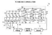
図6には、第1の実施の形態のレベル変換回路10を用いたAD変換回路15を示している。
(Second Embodiment)
Hereinafter, a second embodiment of the present invention will be described with reference to the drawings.
FIG. 6 shows an
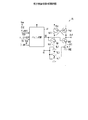
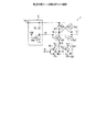
本実施の形態のAD変換回路15は、アナログ信号Vinを4ビットのデジタル信号に変換する逐次比較AD変換回路であり、例えば、自動車用の半導体集積回路装置(LSI)に利用される。AD変換回路15は、レベル変換回路10に加え、第1及び第2のスイッチ回路SW1,SW2、サンプリング容量CS1,CS2,CS3,CS4,CS5、コンパレータ16、レベル変換回路17、逐次比較制御回路18を含む。
The
サンプリング容量CS1〜CS5はその容量値が2の重み付けによる値で設定され、その容量値の比率は1:1:2:4:8に設定されている。すなわち、容量CS1,CS2は1つの単位容量Cxで構成され、容量CS3は2つの単位容量Cxで構成され、容量CS4は4つの単位容量Cxで構成され、容量CS5は8つの単位容量Cxで構成されて計16個の容量群で構成されている。 The sampling capacitors CS1 to CS5 have capacitance values set by weighting values of 2, and the capacitance value ratio is set to 1: 1: 2: 4: 8. That is, the capacitors CS1 and CS2 are composed of one unit capacitor Cx, the capacitor CS3 is composed of two unit capacitors Cx, the capacitor CS4 is composed of four unit capacitors Cx, and the capacitor CS5 is composed of eight unit capacitors Cx. Thus, it is composed of a total of 16 capacity groups.
各サンプリング容量CS1〜CS5の一方の端子はコンパレータ16に接続され、その他方の端子は第1のスイッチ回路SW1に接続されている。第1のスイッチ回路SW1は第2のスイッチ回路SW2に接続されている。各スイッチ回路SW1,SW2は、レベル変換回路10から出力される制御信号に基づいて、サンプリング容量CS1〜CS5に、それぞれ基準電位(リファレンス電位)Vrefと、同基準電位VrefとグランドGNDのレベルとの間で変動するアナログ信号Vinと、グランドGNDとのいずれかのレベルが入力されるように切り替えられる。
One terminal of each of the sampling capacitors CS1 to CS5 is connected to the
コンパレータ16は、高耐圧のPMOSトランジスタPH10,PH11,PH12と、高耐圧のNMOSトランジスタNH10,NH11,NH12,NH13,NH14,NH15と、結合容量CC1,CC2とを含む。コンパレータ16において、PMOSトランジスタPH10とNMOSトランジスタNH10とが直列に接続されて1段目のCMOSインバータ回路19aが構成され、そのインバータ回路19aに並列にNMOSトランジスタNH13が接続されている。また、PMOSトランジスタPH11とNMOSトランジスタNH11とが直列に接続されて2段目のCMOSインバータ回路19bが構成され、そのインバータ回路19bに並列にNMOSトランジスタNH14が接続されている。さらに、PMOSトランジスタPH12とNMOSトランジスタNH12とが直列に接続されて3段目のCMOSインバータ回路19cが構成され、そのインバータ回路19cに並列にNMOSトランジスタNH15が接続されている。各段のインバータ回路19a〜19cには電源電圧Vpp(=5V)が供給されている。また、各NMOSトランジスタNH13〜NH15のゲートにはサンプリング制御信号SPLが供給され、その制御信号SPLに基づいて各NMOSトランジスタNH13〜NH15のオン/オフが制御される。
The
インバータ回路19aの入力(各MOSトランジスタPH10,NH10のゲート)が各サンプリング容量CS1〜CS5に接続され、インバータ回路19aの出力(各MOSトランジスタPH10,NH10のドレイン)は、結合容量CC1を介してインバータ回路19bの入力(各MOSトランジスタPH11,NH11のゲート)に接続される。また、インバータ回路19bの出力(各MOSトランジスタPH11,NH11のドレイン)は、結合容量CC2を介してインバータ回路19cの入力(各MOSトランジスタPH12,NH12のゲート)に接続され、このインバータ回路19cから出力される信号がレベル変換回路17に供給される。
The input of the
レベル変換回路17は、信号振幅を5Vから1.8Vに変換する降圧用のレベル変換回路であり、変換後の信号を逐次比較制御回路18に供給する。そのレベル変換回路17の具体的な回路例を図7に示す。すなわち、レベル変換回路17は、高耐圧のPMOSトランジスタPH16,PH17と高耐圧のNMOSトランジスタNH16〜NH19と低耐圧のPMOSトランジスタPL18,PL19とを含む。1.8Vの電源とグランド間には、PMOSトランジスタPL18とNMOSトランジスタNH18とが直列に接続されるとともに、PMOSトランジスタPL19とNMOSトランジスタNH19とが直列に接続されている。また、PMOSトランジスタPL18のゲートがPMOSトランジスタPL19のドレインに接続され、PMOSトランジスタPL19のゲートがPMOSトランジスタPL18のドレインに接続されている。
The
そして、NMOSトランジスタNH18のゲートには、入力信号INがPMOSトランジスタPH16とNMOSトランジスタNH16からなるインバータ回路20aを介して反転されて入力される。また、NMOSトランジスタNH19のゲートには、インバータ回路20aの出力信号がPMOSトランジスタPH17とNMOSトランジスタNH17からなるインバータ回路20bを介して反転されて入力される。入力信号INは、信号振幅が5Vの信号であり、各インバータ回路20a,20bには、5Vの電源電圧Vppが供給されている。
The input signal IN is inverted and input to the gate of the NMOS transistor NH18 via the
従って、入力信号INがHレベル(5V)である場合、インバータ回路20aの出力ノードはLレベル(0V)となり、インバータ回路20bの出力ノードはHレベル(5V)となるため、レベル変換回路17は、Lレベル(0V)の出力信号OUTを逐次比較制御回路18に供給する。一方、入力信号INがLレベル(0V)である場合、インバータ回路20aの出力ノードはHレベル(5V)となり、インバータ回路20bの出力ノードはLレベル(0V)となるため、レベル変換回路17は、Hレベル(1.8V)の出力信号OUTを逐次比較制御回路18に供給する。
Accordingly, when the input signal IN is at the H level (5V), the output node of the
逐次比較制御回路18は、レベル変換回路17の出力信号に基づいて比較制御を実施し、コンパレータ16とスイッチ回路SW1,SW2とを制御するための制御信号をレベル変換回路10に供給する。レベル変換回路10は、1.8Vの入力信号INを5Vに変換し、変換後の5Vの出力信号に基づいて各スイッチ回路SW1,SW2を制御する。
The successive
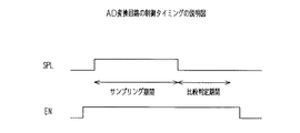
このように構成したAD変換回路15の動作を説明する。
変換を開始する前には、Lレベルの制御信号SPLにより各NMOSトランジスタNH13〜NH15はオフしている。変換を開始すると、先ず、アナログ信号Vinをサンプリングするために、逐次比較制御回路18は制御信号SPLをHレベルとして各NMOSトランジスタNH13〜NH15をオンする。NMOSトランジスタNH13がオンすると、各容量の出力ノードDACOUTとノードN50の電位が等しくなり、NMOSトランジスタNH14がオンすると、ノードN51とノードN52の電位が等しくなる。また、NMOSトランジスタNH15がオンすると、ノードN53とノードN54の電位が等しくなる。PMOSトランジスタPH10とNMOSトランジスタNH10とはコンパレータ16の1段目を構成しており、NMOSトランジスタNH13がオンすると、出力ノードDACOUTとノードN50の電位は、コンパレータ16における1段目の論理しきい値(インバータ回路19aのしきい値)VTLとなる。同様に、各NMOSトランジスタNH14,NH15がオンすることで、ノードN51,N52,N53,N54の電位も論理しきい値VTLとなる。
The operation of the
Before starting the conversion, the NMOS transistors NH13 to NH15 are turned off by the L level control signal SPL. When the conversion is started, first, the successive
制御信号SPLをHレベルとしてサンプリング動作に入ると、出力ノードDACOUTを電位VTLに保った状態で、各容量CS1〜CS5の全てがスイッチ回路SW1及びSW2を介してアナログ入力端子に接続される。これにより、アナログ信号Vinが供給されて各容量CS1〜CS5は該アナログ信号Vinの電位に充電される。 When the control signal SPL is set to the H level and the sampling operation is started, all of the capacitors CS1 to CS5 are connected to the analog input terminals via the switch circuits SW1 and SW2 while the output node DACOUT is kept at the potential VTL. As a result, the analog signal Vin is supplied and the capacitors CS1 to CS5 are charged to the potential of the analog signal Vin.
サンプリング動作の終了後、比較動作に入り、最上位ビット(MSB)から順番にデジタルデータを決定していく。具体的には、例えば、Lレベルの制御信号SPLによってNMOSトランジスタNH15をオフした後、容量CS1〜CS5の一方のノードについて、各スイッチ回路SW1,SW2を制御することで、容量CS1〜CS4をグランドGNDの端子に接続し、容量CS5をリファレンス電位Vrefの端子に接続する。このとき、電荷の再分配で決まる出力ノードDACOUTの電位は、Vref/2−Vin+VTLとなり、アナログ信号Vinの電位が、リファレンス電位Vrefの1/2より大きいか小さいかを、コンパレータ16の1段目(トランジスタPH10,NH10)、2段目(トランジスタPH11,NH11)、3段目(トランジスタPH12,NH12)の回路19a,19b,19cで判定する。そして、その判定結果としてノードN54から出力される信号レベルに基づいてMSBが決定される。
After completion of the sampling operation, the comparison operation is started, and digital data is determined in order from the most significant bit (MSB). Specifically, for example, after the NMOS transistor NH15 is turned off by the L level control signal SPL, the capacitors CS1 to CS4 are grounded by controlling the switch circuits SW1 and SW2 for one node of the capacitors CS1 to CS5. Connected to the GND terminal, the capacitor CS5 is connected to the reference potential Vref terminal. At this time, the potential of the output node DACOUT determined by charge redistribution is Vref / 2−Vin + VTL, and the first stage of the
以下同様に、スイッチ回路SW1,SW2を制御することで、Vref/4−Vin+VTLあるいは、3Vref/4−Vin+VTLの電位を生成し、MSB側から順番にデジタルデータが決定される。例えば、容量CS1,CS3〜CS5をグランドGNDの端子に接続し、容量CS2をリファレンス電位Vrefの端子に接続すると、コンパレータ16に入力されるノードDACOUTの電位は、Vref/16−Vin+VTLとなる。つまり、各スイッチ回路SW1,SW2によって各容量CS1〜CS5をリファレンス電位VrefあるいはグランドGNDと接続することにより、各サンプリング容量CS1〜CS5の合計の容量値である16Cxに対して1/16の大きさのCxを単位として、出力ノードDACOUTの電位をVref/16刻みで変化させることができる。これにより、4ビットのデジタルデータが決定される。
Similarly, by controlling the switch circuits SW1 and SW2, a potential of Vref / 4−Vin + VTL or 3Vref / 4−Vin + VTL is generated, and digital data is sequentially determined from the MSB side. For example, when the capacitors CS1, CS3 to CS5 are connected to the terminal of the ground GND and the capacitor CS2 is connected to the terminal of the reference potential Vref, the potential of the node DACOUT input to the
図8には、レベル変換回路10の出力信号により制御されるスイッチ回路の具体的な回路例を示している。
図8に示すように、レベル変換回路10の出力信号OUTは、ナンド回路NAND1の第1入力端子に供給されるとともに、ノア回路NOR1の第1入力端子に供給される。また、比較を開始するための制御信号COMPがナンド回路NAND1の第2入力端子に供給されるとともに、インバータ回路INV1を介して反転されてノア回路NOR1の第2入力端子に供給される。ナンド回路NAND1、ノア回路NOR1、及びインバータ回路INV1は、5Vの電源電圧が供給されて動作するゲート回路である。
FIG. 8 shows a specific circuit example of the switch circuit controlled by the output signal of the
As shown in FIG. 8, the output signal OUT of the
ナンド回路NAND1の出力信号は高耐圧のPMOSトランジスタPH20のゲートに供給され、ノア回路NOR1の出力信号は高耐圧のNMOSトランジスタNH20のゲートに供給されている。各MOSトランジスタPH20,NH20のドレインは互いに接続されており、その接続部がサンプリング容量CS1に接続されている。また、PMOSトランジスタPH20のソースにリファレンス電位Vrefが供給され、NMOSトランジスタNH20のソースはグランドGNDに接続されている。さらに、各MOSトランジスタPH20,NH20と容量CS1の接続部には、スイッチ回路SW3が接続されており、そのスイッチ回路SW3を介してアナログ信号(入力電圧)Vinが供給されるよう構成されている。 The output signal of the NAND circuit NAND1 is supplied to the gate of the high breakdown voltage PMOS transistor PH20, and the output signal of the NOR circuit NOR1 is supplied to the gate of the high breakdown voltage NMOS transistor NH20. The drains of the MOS transistors PH20 and NH20 are connected to each other, and the connection is connected to the sampling capacitor CS1. The reference potential Vref is supplied to the source of the PMOS transistor PH20, and the source of the NMOS transistor NH20 is connected to the ground GND. Further, a switch circuit SW3 is connected to a connection portion between each of the MOS transistors PH20 and NH20 and the capacitor CS1, and an analog signal (input voltage) Vin is supplied via the switch circuit SW3.
ここで、AD変換回路15の動作タイミングを説明する。
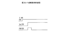
図9に示すように、サンプリング開始と同時あるいはそれ以前に、レベル変換回路10に供給する制御信号ENをHレベルとし、該レベル変換回路10のバイアス回路11に電流を流し活性化させる。バイアス回路11は、制御信号ENをHレベルとして数十nsでバイアス電位NBが定常状態に達するので、数百nsから数千nsのサンプリング期間に対して十分高速に動作時の状態に復帰する。バイアス回路11に電流が流れ、その出力インピーダンスが低い状態で、レベル変換回路10の入力信号INが変化し、それに応答して出力信号OUTも変換する。
Here, the operation timing of the
As shown in FIG. 9, at the same time or before the start of sampling, the control signal EN supplied to the
AD変換回路15のサンプリング期間中(サンプリング制御信号SPLがHレベルである期間)は、Lレベルの制御信号COMPが供給されてPMOSトランジスタPH20とNMOSトランジスタNH20がオフされ、スイッチ回路SW3が閉じられることにより、サンプリング容量CS1がアナログ信号Vinの電位に充電される。 During the sampling period of the AD conversion circuit 15 (period in which the sampling control signal SPL is at the H level), the L level control signal COMP is supplied, the PMOS transistor PH20 and the NMOS transistor NH20 are turned off, and the switch circuit SW3 is closed. Thus, the sampling capacitor CS1 is charged to the potential of the analog signal Vin.
また、比較判定期間には、Hレベルの制御信号COMPが供給され、レベル変換回路10の出力信号OUTに応じて、MOSトランジスタPH20,NH20のいずれか一方がオンし、サンプリング容量CS1が電位Vrefあるいはグランドに接続される。
Further, during the comparison determination period, an H level control signal COMP is supplied, and one of the MOS transistors PH20 and NH20 is turned on according to the output signal OUT of the
比較判定が終了すると、AD変換回路15の信号は変化しなくなるので、制御信号ENをLレベルとし、レベル変換回路10におけるバイアス回路11の電流が停止される。
このように、上記第1の実施の形態のレベル変換回路10を逐次比較AD変換回路15に適用することができる。また、本実施の形態のように、逐次比較AD変換回路15のようなMCUのリソースにレベル変換回路10を適用する場合、MCUが予め各リソースを使用するタイミングを把握しているため、それに先立ってバイアス回路11を活性化し、リソースの使用が終了した時点で、バイアス回路11におけるバイアス電流を削減することができる。
When the comparison determination is completed, the signal of the
As described above, the
(第3の実施の形態)
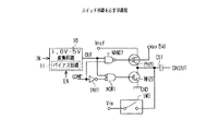
以下、本発明を具体化した第3の実施の形態を説明する。
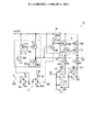
図10には、本実施の形態のレベル変換回路22を示している。このレベル変換回路22は、バイアス回路23の回路構成を変更した点と低耐圧のPMOSトランジスタPL3とNMOSトランジスタNL3からなるインバータ回路24を追加した点が上記第1の実施の形態におけるレベル変換回路10と相違する。図10において、第1の実施の形態と同様の構成については同一の符号を付してその説明を一部省略し、以下には、その相違点を中心に説明する。
(Third embodiment)
Hereinafter, a third embodiment of the present invention will be described.
FIG. 10 shows the
インバータ回路3の出力ノードN10の電位は、PMOSトランジスタPH1の駆動電流を越えてNMOSトランジスタNH1,NL1に電流が流れて放電されることにより、HレベルからLレベルに変化するので、回路設計によっては出力ノードN10の立ち下がりが遅くなる。また、上記レベル変換回路10では、そのインバータ回路3の出力ノードN10の電位をインバータ回路4で反転する構成であるため、回路設定によってはインバータ回路4の出力ノードN11の立ち上がりが遅れる場合がある。これに対して、本実施の形態のレベル変換回路22において、インバータ回路4の出力ノードN11の電位は、インバータ回路3の出力ノードN10の論理レベルを反転して生成する構成ではなく、別に設けたインバータ回路24の出力ノードの論理レベルを反転する構成である。この構成とすることで、より確実な回路設計が可能となる。
The potential of the output node N10 of the
次に、本実施の形態におけるバイアス回路23の構成について説明する。
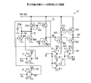
バイアス回路23は、高耐圧のPMOSトランジスタPH3,PH4、高耐圧のNMOSトランジスタNH3,NH4,NH5、抵抗R1,R3、及び容量CPORを含む。このバイアス回路23において、高耐圧のPMOSトランジスタPH3,PH4、高耐圧のNMOSトランジスタNH3,NH4、抵抗R1、及び容量CPORの接続構成は、第1の実施の形態におけるバイアス回路11と同じであるため、ここでは、その説明を省略する。
Next, the configuration of the
The
本実施の形態のバイアス回路23は、第1の実施の形態と相違して、PMOSトランジスタPH4のドレイン(各PMOSトランジスタPH3,PH4のゲートの接続ノードN30)が抵抗R3とNMOSトランジスタNH5を介してグランドに接続される。このNMOSトランジスタNH5のゲートには、制御信号PDをインバータ回路(PMOSトランジスタPL5とNMOSトランジスタNL5とからなるCMOSインバータ回路)25を介して反転した制御信号PDXが供給される。なお、通常は、制御信号PDがLレベル、制御信号PDXがHレベルに制御されている。
In the
上記バイアス回路11において、供給される制御信号ENがLレベルである場合、NMOSトランジスタNH4がオフするため、PMOSトランジスタPH3には反転領域での電流が流れず、各MOSトランジスタPH3,NH3に流れるリーク電流によって、バイアス電位NBが定まる。
In the
ここで、例えば、上記第1実施の形態のレベル変換回路10をP型基板、nwellプロセスで製造する場合を想定する。その場合、PMOSトランジスタPH3のドレイン接合は、電源電圧Vppとバイアス電位NB間に逆方向のpn接合を含み、NMOSトランジスタNH3のドレイン接合は、バイアス電位NBとグランドGND間に逆方向のpn接合を含む。これら逆方向のpn接合に流れるリーク電流について、例えば、PMOSトランジスタPH3のドレイン接合の面積を大きくしておいて、該トランジスタPH3からのリーク電流が大きくなるようにレイアウトを工夫する。それにより、バイアス電位NBが想定している電位(電源電圧Vddから高耐圧のNMOSトランジスタのしきい値電圧Vth高い電位かそれより多少低い電位)に設計することも可能である。これに対し、図10に示すバイアス回路23を用いることで、より確実かつ簡単にバイアス電位NBの設計をすることができる。
Here, for example, a case is assumed where the
このバイアス回路23において、例えば、抵抗R1の抵抗値を400キロオームとし、抵抗R3の抵抗値を4000キロオームとする。また、電源電圧Vppが5V、PMOSトランジスタPH4のしきい値電圧Vthが1Vとすると、制御信号ENがHレベルであるとき、抵抗R1には4V/400キロオーム=10uAの電流が流れる。カレントミラー回路を構成するPMOSトランジスタPH3とPMOSトランジスタPH4のゲート幅Wが等しい場合、PMOSトランジスタPH3にも10uAの電流が流れる(制御信号PDがLレベルである場合には、抵抗R3に流れる電流が加算されるので、正確には11uAの電流が流れる)。そして、NMOSトランジスタNH3のゲート幅WをNMOSトランジスタNH1,NH2の10倍に設計する場合、NMOSトランジスタNH1,NH2に流れるリーク電流は1uAに設計することができる。
In the
また、制御信号ENがLレベルであり、制御信号PDがLレベルである場合、抵抗R1には電流が流れず、抵抗R3だけに電流が流れる。この場合、PMOSトランジスタPH3には1uAの電流が流れ、NMOSトランジスタNH1,NH2に流れるリーク電流は0.1uAとすることができる。 Further, when the control signal EN is at the L level and the control signal PD is at the L level, no current flows through the resistor R1, and a current flows only through the resistor R3. In this case, a current of 1 uA flows through the PMOS transistor PH3, and a leakage current flowing through the NMOS transistors NH1 and NH2 can be 0.1 uA.
このように、バイアス回路23には、レベル変換回路22が動作しているときに大電流(上述した10uAの電流)を流す抵抗R1と、レベル変換回路22の出力が変化しないときに小さい電流(上述した1uAの電流)を流す抵抗R3とを設けた。この構成によれば、レベル変換回路22の出力が変化しない待機時にも、バイアス回路23に流れる電流が正確に設計できる。なお、上記では、抵抗R3に流す電流値を1uAとして説明したが、その電流値は待機時に問題とならない範囲内で適宜変更することができる。
In this way, the
また、レベル変換回路22では、制御信号PDをHレベル(制御信号PDXをLレベル)とすることで、抵抗R3に流れる電流も停止されるので、待機時のバイアス電流1uAが問題となる状況、例えば、IDDQの測定時などには、制御信号PDをHレベルとする。
Further, in the
本実施の形態におけるバイアス回路23では、バイアス電位NBの安定化容量C1を省略したが、必要に応じて容量C1を設けてもよい。また、制御信号PD,PDXは1.8Vの信号として示したが、試験時だけに電流を停止する場合には、制御信号PD,PDXを5Vの信号に変更してもよい。
In the
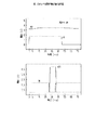
図11は図10のレベル変換回路22の動作を示す波形図である。
なおここでは、高耐圧のNMOSトランジスタのしきい値電圧Vthを約1V、電源電圧Vddを1.8V、電源電圧Vppを5Vとした場合の動作を示す。また、レベル変換回路22では入力信号INと出力信号OUTとが同相の信号となる(信号波形が重なり分かりにくくなる)ため、入力信号INと逆相となるノードN20の信号波形を示している。
FIG. 11 is a waveform diagram showing the operation of the
Here, the operation when the threshold voltage Vth of the high breakdown voltage NMOS transistor is about 1 V, the power supply voltage Vdd is 1.8 V, and the power supply voltage Vpp is 5 V is shown. Further, in the
時刻0において、制御信号ENをHレベルに変化させることで、バイアス回路23にバイアス電流が流れ、バイアス電位NBが増加する。時刻30ns〜40nsの期間で入力信号INをHレベルからLレベルに変化させると、出力信号OUT(図11ではノードN20の電位)がそれに応じて変化する。そして、時刻50nsで制御信号ENをLレベルに変化させることで、バイアス電位NBは待機状態に戻る。なおこのとき、制御信号PDXは1.8Vの信号レベル(Hレベル)を保っている。
By changing the control signal EN to H level at
同図に示されるように、制御信号ENをHレベルとすることで、バイアス電位NBが動作時の値まで上昇し、制御信号ENをLレベルとすることで、バイアス電位NBがゆっくりと下がる。高耐圧のNMOSトランジスタのしきい値電圧Vthは約1Vとしたが、基板バイアス効果によって、バイアス電位NBは3.5V程度となっている。 As shown in the figure, by setting the control signal EN to the H level, the bias potential NB increases to the value at the time of operation, and by setting the control signal EN to the L level, the bias potential NB slowly decreases. The threshold voltage Vth of the high breakdown voltage NMOS transistor is about 1 V, but the bias potential NB is about 3.5 V due to the substrate bias effect.
以上記述したように、本実施の形態によれば、以下の効果を奏する。
(1)バイアス回路23におけるバイアス電流を決定する抵抗を2つ用意し、それぞれの抵抗R1,R3の電流値を待機時と動作時に必要となる適切な電流値に設計することで、待機時におけるバイアス電流の設計をより容易に行うことができる。また、必要なときにだけ、バイアス回路23に流す電流を大きくして、バイアス電位NBの等価インピーダンスを下げることができる。なお、このバイアス電流の制御により、レベル変換機能自体は悪影響を受けることはない。
As described above, according to the present embodiment, the following effects can be obtained.
(1) Two resistors for determining the bias current in the
(2)レベル変換回路22において、インバータ回路4の出力ノードN11の電位は、インバータ回路3とは別に設けたインバータ回路24の出力を反転して生成されるので、回路動作の高速化を図ることができる。
(2) In the
(第4の実施の形態)
以下、本発明を具体化した第4の実施の形態を説明する。
図12には、本実施の形態のレベル変換回路27を示している。このレベル変換回路27は、入力信号INを受けるインバータ回路3,4のPMOSトランジスタPL1,PL2を省略した点が第3の実施の形態におけるレベル変換回路22と相違する。図12において、第3の実施の形態と同様の構成については同一の符号を付してその説明を省略し、以下には、その相違点を中心に説明する。
(Fourth embodiment)
Hereinafter, a fourth embodiment of the present invention will be described.
FIG. 12 shows the
すなわち、図10のレベル変換回路22において、ノードN10,N11がHレベルである場合、PMOSトランジスタPL1,PL2がオンすることで電源電圧Vddのレベルとなる。従って、レベル変換回路22は、PMOSトランジスタPL1,PL2を設けることで、ノードN10,N11のHレベルを直接的に電源電圧Vddに設計することができる。また、入力信号INの変化時には、ノードN10,N11のいずれか一方のノードがPMOSトランジスタPL1,PL2により、電源電圧Vddに充電されるので、NMOSトランジスタNH1,NH2がオフするタイミングが早くなる利点がある。
That is, in the
これに対し、本実施の形態のレベル変換回路27では、PMOSトランジスタPL1,PL2を使用しない回路構成となっている。これらPMOSトランジスタPL1,PL2がない場合でも、バイアス回路23で発生するバイアス電位NBはVdd+Vthの電位となるので、NMOSトランジスタNH1,NH2のドレイン電位はほぼVddに設計することができる。なお、図12のバイアス回路23では、容量CPORを省略して図示しているが、必要であれば容量CPORを設けてもよい。
In contrast, the
本実施の形態のレベル変換回路27は、上記第3の実施の形態におけるレベル変換回路22と同様に動作する。また、レベル変換回路27では、バイアス電位NBが過渡的な電位あるいは、意図しない状態(中間電位)にありかつ、電源電圧Vppが0Vのときに意図しない電流が流れないといった利点がある。例えば、バイアス電位NBを電源電圧Vdd、Vppとは別の電源電圧から作るような場合には、レベル変換回路27の回路構成が必須になる。すなわち、1.8V,5V,3.3Vの電源電圧の回路が混在するLSIで、3.3Vの電源電圧からバイアス電位NBを作り、1.8Vから5Vへのレベル変換を行う場合を想定する。また、5Vの電源電圧Vppが0Vで、電源電圧Vddが1.8V、かつバイアス電位NBがVdd+Vthである場合、図10のように、PMOSトランジスタPL1,PL2があるレベル変換回路22では、入力信号INがLレベルであるときにノードN10の電位は1.8Vとなる。電源電圧Vppが0Vになると、PMOSトランジスタPH1のバックゲートの電位も0Vとなる。NMOSトランジスタNH1のゲート電位として供給されるバイアス電位NBはVdd+Vthなので、NMOSトランジスタNH1がオンする。このとき、PMOSトランジスタPL1とNMOSトランジスタNH1の経路を通ってPMOSトランジスタPH1のバックゲートに電流が流れてしまう。
The
一方、本実施の形態のレベル変換回路27は、PMOSトランジスタPL1,PL2を使用しない回路構成であるため、電源電圧Vppが0V、バイアス電位NBがVdd+Vthであっても、電源電圧Vddから電流を供給する経路が存在しないので、PMOSトランジスタPH1のバックゲートに流れる意図しない電流(望ましくない電流)が流れることを回避することができる。
On the other hand,
このように、本実施の形態のレベル変換回路27では、バイアス電位NBにかかわらず、電源電圧Vppと電源電圧Vddとの分離が容易となる。つまり、バイアス電位NBを電源電圧Vpp以外の電源電圧から発生する場合、レベル変換回路27のように、PMOSトランジスタPL1,PL2を省略した回路構成としたほうが、電源間を確実に分離することができる。
Thus, in the
(第5の実施の形態)
以下、本発明を具体化した第5の実施の形態を説明する。
図13には、本実施の形態のレベル変換回路28を示している。このレベル変換回路28は、各MOSトランジスタPH1,PH2,PL1,PL2,NH1,NH2,NL1,NL2からなる変換部29a,29b,・・・を複数段設けた点が第1の実施の形態におけるレベル変換回路10と相違する。図12において、第1の実施の形態と同様の構成については同一の符号を付している。
(Fifth embodiment)
The fifth embodiment of the present invention will be described below.
FIG. 13 shows the
レベル変換回路28において各変換部29a,29bを構成する各MOSトランジスタPH1,PH2,PL1,PL2,NH1,NH2,NL1,NL2の接続構成は、第1の実施の形態と同じである。このレベル変換回路28において、各段の変換部29a,29b,・・・には、それぞれ1.8Vの入力信号IN1,IN2,・・・が供給され、それら入力信号に対応する5Vの出力信号OUT1,OUT2,・・・が出力される。また、バイアス回路11で発生したバイアス電位NBは、各段の変換部29a,29bにおけるNMOSトランジスタNH1,NH2に供給されている。なお、図13のバイアス回路11では、容量CPOR,C1を省略して図示しているが、必要であれば容量CPOR,C1を設けてもよい。
In the
このように、本実施の形態のレベル変換回路28では、複数の変換部29a,29b,・・・でバイアス回路11が共通化されている。よって、各変換部の動作期間が同じになるよう設計することで、レベル変換回路28の出力が変化しない期間にバイアス回路11のバイアス電流を削減するといった制御を容易に行うことができる。
As described above, in the
(第6の実施の形態)
以下、本発明を具体化した第6の実施の形態を説明する。
図14は、本実施の形態のレベル変換回路30を示している。このレベル変換回路30は、バイアス回路31,32の構成が第4の実施の形態におけるレベル変換回路27と相違する。図14において、第4の実施の形態と同様の構成については同一の符号を付してその説明を省略し、以下には、その相違点を中心に説明する。
(Sixth embodiment)
The sixth embodiment of the present invention will be described below.
FIG. 14 shows the
上記第4の実施の形態のバイアス回路23では、NMOSトランジスタNH3に流れるバイアス電流を抵抗R1で決定する回路構成であるが、本実施の形態では、より複雑な回路構成でバイアス電流を決定している。
The
具体的に、バイアス回路31は、高耐圧のPMOSトランジスタPH3と高耐圧のNMOSトランジスタNH3とを含む。PMOSトランジスタPH3とNMOSトランジスタNH3とは直列に接続されており、PMOSトランジスタPH3のソースに5Vの電源電圧Vppが供給されている。NMOSトランジスタNH3はダイオード接続されており、そのソースに1.8Vの電源電圧Vddが供給されている。PMOSトランジスタPH3のゲートはバイアス回路32に接続されている。また、各MOSトランジスタPH3,NH3のドレインの接続部からバイアス電位NBが出力され、そのバイアス電位NBが各NMOSトランジスタNH1,NH2のゲートに供給される。
Specifically, the
バイアス回路32は、高耐圧のPMOSトランジスタPH23,PH24,PH25,PH26と、高耐圧のNMOSトランジスタNH25,NH26,NH27と、抵抗R4,R5とを含む。各PMOSトランジスタPH23〜PH26のソースは互いに接続され該各ソースに電源電圧Vppが供給される。PMOSトランジスタPH23のドレインは、PMOSトランジスタPH26のゲートに接続されるとともに、抵抗R4を介してNMOSトランジスタNH25のドレインに接続されている。NMOSトランジスタNH25のソースはグランドに接続され、このNMOSトランジスタNH25のゲートに1.8Vの制御信号ENが供給される。
The
各PMOSトランジスタPH23,PH24,PH25の各ゲートは互いに接続されるとともに、バイアス回路31のPMOSトランジスタPH3のゲートにも接続されている。該各ゲートは、PMOSトランジスタPH25のドレインとNMOSトランジスタNH27のドレインに接続される。また、PMOSトランジスタPH24,PH26とNMOSトランジスタNH26の各ドレインは互いに接続され、そのドレインはNMOSトランジスタNH26,NH27のゲートに接続されている。NMOSトランジスタNH26のソースはグランドに接続され、NMOSトランジスタNH27のソースは抵抗R5を介してグランドに接続されている。
The gates of the PMOS transistors PH23, PH24, and PH25 are connected to each other and also connected to the gate of the PMOS transistor PH3 of the
また、制御信号ENは、低耐圧のPMOSトランジスタPL22とNMOSトランジスタNL20からなるインバータ回路33で反転され、反転された制御信号ENXが低耐圧のNMOSトランジスタNL21のゲートに供給されている。そして、そのNMOSトランジスタNL21は、ドレインがバイアス回路32における各NMOSトランジスタNH26,NH27のゲートに接続され、ソースがグランドに接続されている。
The control signal EN is inverted by the inverter circuit 33 including the low breakdown voltage PMOS transistor PL22 and the NMOS transistor NL20, and the inverted control signal ENX is supplied to the gate of the low breakdown voltage NMOS transistor NL21. The NMOS transistor NL21 has a drain connected to the gates of the NMOS transistors NH26 and NH27 in the
バイアス回路32において、PMOSトランジスタPH24,PH25、NMOSトランジスタNH26,NH27、及び抵抗R5で構成されるカレントミラーループは自己バイアス回路としてよく知られている回路部分である。このカレントミラーループによりバイアス回路31のバイアス電流が決定される。この場合、抵抗R5の抵抗値を小さくすることができるといった利点がある。例えば、NMOSトランジスタNH26,NH27がサブスレッショルド領域で動作しているときには、各MOSトランジスタPH24,PH25,NH26,NH27、及び抵抗R5に流れる電流は、熱電圧(kT/q、k:ボルツマン定数、T:絶対温度、q:電子電荷)程度の電圧を抵抗R5の抵抗値で割った値に定まる。
In the
そして、その自己バイアス回路のバイアス電位(ノードN30の電位)をバイアス回路31のPMOSトランジスタPH3のゲートに供給することで、自己バイアス回路で決定した電流をPMOSトランジスタPH3に流すことができる。
Then, by supplying the bias potential of the self-bias circuit (the potential of the node N30) to the gate of the PMOS transistor PH3 of the
バイアス回路32において、PMOSトランジスタPH23,PH26、NMOSトランジスタNH25、及び抵抗R4はスタートアップ回路として働く。制御信号ENがHレベルであるとき、NMOSトランジスタNH25がオンする。このとき、PMOSトランジスタPH24,PH25に電流が流れていないと、PMOSトランジスタPH26のゲート電位は0Vとなる。
In the
PMOSトランジスタPH26のゲート電位が0Vとなると、NMOSトランジスタNH26に電流が流れ始め、カレントミラーループ(各MOSトランジスタPH24,PH25,NH26,NH27、抵抗R5)に電流が流れて安定点に達する。PMOSトランジスタPH24,PH25に電流が流れると、PMOSトランジスタPH23にも電流が流れ、PMOSトランジスタPH26のゲート電位が電源電圧Vppとなってスタートアップ回路が切り離される。 When the gate potential of the PMOS transistor PH26 becomes 0V, a current starts to flow through the NMOS transistor NH26, and a current flows through the current mirror loop (each MOS transistor PH24, PH25, NH26, NH27, resistor R5) to reach a stable point. When a current flows through the PMOS transistors PH24 and PH25, a current also flows through the PMOS transistor PH23, the gate potential of the PMOS transistor PH26 becomes the power supply voltage Vpp, and the startup circuit is disconnected.
バイアス回路32にHレベルの制御信号ENが供給される場合、スタートアップ回路が動作するので、バイアス回路32がスタートアップし、それに伴いバイアス回路31のNMOSトランジスタNH3にバイアス電流が流れる。一方、Lレベルの制御信号ENが供給される場合、スタートアップ回路に電流が流れず、該スタートアップ回路は機能しない。またこのとき、Hレベルの制御信号ENXによりNMOSトランジスタNL21がオンするので、各NMOSトランジスタNH26,NH27がオフし、バイアス回路32に流れる電流が0となる。
When the H level control signal EN is supplied to the
このように、複雑な回路構成のバイアス回路32を用いても、第4の実施の形態と同様に、1.8Vの制御信号ENによって、バイアス回路32に流れる電流をオン/オフ制御することができる。
As described above, even when the
(第7の実施の形態)
以下、本発明を具体化した第7の実施の形態を説明する。
図15は、本実施の形態のレベル変換回路35を示している。
(Seventh embodiment)
The seventh embodiment of the present invention will be described below.
FIG. 15 shows the
上記第6の実施の形態では、バイアス回路32に流れる電流を制御信号ENで直接オン/オフ制御するものであったが、本実施の形態のレベル変換回路35では、バイアス回路32に流れる電流を別の制御信号PDでオン/オフ制御し、カレントミラー比により電流増幅する回路部分を制御信号ENでオン/オフ制御する。そして、その回路部分で発生する電位によりバイアス回路31に流れるバイアス電流を制御するようにしている。図15において、第6の実施の形態と同様の構成については同一の符号を付してその説明を省略し、以下には、その相違点を中心に説明する。
In the sixth embodiment, the current flowing through the
バイアス回路32におけるPMOSトランジスタPH25のソースに、高耐圧のPMOSトランジスタPH26,PH27のソースが接続され、PMOSトランジスタPH25のゲートとドレインとの接続部に、PMOSトランジスタPH26のゲートが接続されている。PMOSトランジスタPH26のドレインが、ダイオード接続されたNMOSトランジスタNH28を介してグランドに接続されている。
In the
PMOSトランジスタPH27は、ゲートとドレインとが接続され、その接続部はNMOSトランジスタNH29のドレインと接続されるとともに、バイアス回路31におけるPMOSトランジスタPH3のゲートに接続されている。NMOSトランジスタNH29は、ソースがグランドに接続され、ゲートはNMOSトランジスタNL24を介してPMOSトランジスタPH26とNMOSトランジスタNH28の接続部(ドレイン)に接続されている。また、NMOSトランジスタNH29のゲートは、NMOSトランジスタNL25を介してグランドに接続されている。
The PMOS transistor PH27 has a gate and a drain connected to each other, and the connection is connected to the drain of the NMOS transistor NH29 and to the gate of the PMOS transistor PH3 in the
そして、制御信号ENは、NMOSトランジスタNL24のゲートに供給されるとともに、PMOSトランジスタPL24とNMOSトランジスタNL26とからなるインバータ回路を介して反転されてNMOSトランジスタNL25のゲートに供給される。 The control signal EN is supplied to the gate of the NMOS transistor NL24, is inverted through an inverter circuit including the PMOS transistor PL24 and the NMOS transistor NL26, and is supplied to the gate of the NMOS transistor NL25.
本実施の形態のレベル変換回路35において、バイアス回路32で発生されるPMOSトランジスタPH25のゲート電位が、そのPMOSトランジスタPH25とカレントミラー回路を構成するPMOSトランジスタPH26のゲートに供給され、そのゲート電位に応じた電流がNMOSトランジスタNH28に流れる。このNMOSトランジスタNH28のゲート電位は、Hレベルの制御信号ENによりオンしたNMOSトランジスタNL24を介してNMOSトランジスタNH29のゲートに伝達される。NMOSトランジスタNH29に流れる電流がPMOSトランジスタPH27で電圧(ノード30の電位)に変換されて、バイアス回路31のPMOSトランジスタPH3のゲートに供給される。これにより、バイアス回路31におけるPMOSトランジスタPH3とNMOSトランジスタNH3にバイアス電流を流す。
In the
このレベル変換回路35において、各MOSトランジスタPH25,PH26,NH28,NH29,PH3の比を適切に設計することで、バイアス回路32の電流を実用上十分に小さくすることができ、バイアス回路31におけるPMOSトランジスタPH3の電流を必要な大きさに設計することができる。
In this
また、レベル変換回路35では、NMOSトランジスタNH28のゲート電位をNMOSトランジスタNL24でNMOSトランジスタNH29に伝える構成であるので、制御信号ENがHレベルであるときだけ、NMOSトランジスタNL24がオンしてゲート電位が伝達されてNMOSトランジスタNH29に電流が流れる。また、制御信号ENがLレベルであるときは、ゲート電位の伝達が遮断されるとともに、NMOSトランジスタNL25がオンしてNMOSトランジスタNH29のゲートがグランドに接続されるため、NMOSトランジスタNH29には電流が流れない。このように構成すると、信号振幅が1.8Vである制御信号ENによってバイアス回路31のバイアス電流を制御することができる。
Further, since the
なお、制御信号ENがLレベルであるときに電流を流すPMOSトランジスタを、バイアス回路31におけるPMOSトランジスタPH3と並列に設けてもよい。また、そのPMOSトランジスタのゲート電位は、PMOSトランジスタPH25のゲート電位とすることができる。
Note that a PMOS transistor that allows a current to flow when the control signal EN is at the L level may be provided in parallel with the PMOS transistor PH3 in the
(第8の実施の形態)
以下、本発明を具体化した第8の実施の形態を説明する。
図16は、本実施の形態の原理説明図である。本実施の形態のレベル変換回路40は、バイアス回路41における通常時のバイアス電流のオン/オフ制御を低い電源電圧Vdd(1.8V)の制御信号ENで行う。また、待機時のバイアス電流のオン/オフ制御を高い電源電圧Vpp(5V)の制御信号PDHで行う。
(Eighth embodiment)
The eighth embodiment of the present invention will be described below.
FIG. 16 is an explanatory diagram of the principle of the present embodiment. The
図17は、本実施の形態におけるレベル変換回路40の回路構成を示す回路図である。
レベル変換回路40は、第6の実施の形態におけるレベル変換回路30(図14参照)での制御信号ENを5Vの制御信号PDHに置き換えている。さらに、1.8Vの制御信号ENでオン/オフ制御する電流を、第1の実施の形態におけるレベル変換回路10(図5参照)と同様に抵抗R1で発生している。図17において、第1及び第6の実施の形態と同様の構成については同一の符号を付している。
FIG. 17 is a circuit diagram showing a circuit configuration of the
The
すなわち、レベル変換回路40は、上記バイアス回路31,32を構成する回路素子に加え、高耐圧のPMOSトランジスタPH28,PH29,PH30,PH31,PH32、高耐圧のNMOSトランジスタNH4,NH30,NH31、及び抵抗R1を含む。
That is, the
5Vの制御信号PDHは、PMOSトランジスタPH28とNMOSトランジスタNH30とからなるインバータ回路42に供給され、該インバータ回路42で反転された制御信号PDHXがNMOSトランジスタNH31のゲートに供給される。このNMOSトランジスタNH31は、ドレインがNMOSトランジスタNH26,NH27のゲートに接続され、ソースがグランドに接続されている。 The control signal PDH of 5V is supplied to the inverter circuit 42 composed of the PMOS transistor PH28 and the NMOS transistor NH30, and the control signal PDHX inverted by the inverter circuit 42 is supplied to the gate of the NMOS transistor NH31. The NMOS transistor NH31 has a drain connected to the gates of the NMOS transistors NH26 and NH27, and a source connected to the ground.
また、5Vの制御信号PDHは、PMOSトランジスタPH29,PH30とNMOSトランジスタNH25のゲートに供給されている。PMOSトランジスタPH29は、ソースに電源電圧Vppが供給され、ドレインがPMOSトランジスタPH26のゲートに接続されている。PMOSトランジスタPH30は、ソースに電源電圧Vppが供給され、ドレインが各PMOSトランジスタPH3,PH23,PH24,PH25のゲートに接続されている。 The 5V control signal PDH is supplied to the gates of the PMOS transistors PH29 and PH30 and the NMOS transistor NH25. In the PMOS transistor PH29, the power supply voltage Vpp is supplied to the source, and the drain is connected to the gate of the PMOS transistor PH26. In the PMOS transistor PH30, the power supply voltage Vpp is supplied to the source, and the drain is connected to the gates of the PMOS transistors PH3, PH23, PH24, and PH25.
各PMOSトランジスタPH31,PH32のソースに5Vの電源電圧Vppが供給され、PMOSトランジスタPH31のゲートとPMOSトランジスタPH32のゲートとが互いに接続されるとともに、各ゲートはPMOSトランジスタPH32のドレインに接続されている。 A source voltage Vpp of 5 V is supplied to the sources of the PMOS transistors PH31 and PH32, the gate of the PMOS transistor PH31 and the gate of the PMOS transistor PH32 are connected to each other, and each gate is connected to the drain of the PMOS transistor PH32. .
PMOSトランジスタPH32のドレインは、抵抗R1を介してNMOSトランジスタNH4のドレインに接続されている。このNMOSトランジスタNH4は、ソースがグランドに接続され、ゲートに1.8Vの制御信号ENが供給されている。PMOSトランジスタPH31のドレインは、PMOSトランジスタPH3とNMOSトランジスタNH3との接続部(ドレイン)に接続されている。 The drain of the PMOS transistor PH32 is connected to the drain of the NMOS transistor NH4 via the resistor R1. The NMOS transistor NH4 has a source connected to the ground and a gate supplied with a control signal EN of 1.8V. The drain of the PMOS transistor PH31 is connected to a connection portion (drain) between the PMOS transistor PH3 and the NMOS transistor NH3.
次に、本実施の形態におけるレベル変換回路40の動作について説明する。
レベル変換回路40の動作時には、Hレベル(1.8V)の制御信号ENが供給され、NMOSトランジスタNH4がオンする。このとき、抵抗R1に電流が流れ、その電流はPMOSトランジスタPH32に流れる。すると、PMOSトランジスタPH32とカレントミラー接続されたPMOSトランジスタPH31にも電流が流れ、その電流は、ダイオード接続されたNMOSトランジスタNH3を介して低い電源電圧Vddの電源側に流れ込む。これにより、バイアス回路41のバイアス電位NBは、電源電圧Vddから高耐圧のNMOSトランジスタNH3のしきい値電圧Vth程度高い電圧となる。
Next, the operation of the
During the operation of the
一方、待機時には、Lレベル(0V)の制御信号ENが供給され、NMOSトランジスタNH4がオフするため、PMOSトランジスタPH31に流れる電流が停止される。また、この待機時においては、制御信号PDHによって、PMOSトランジスタPH3に流れる電流がオン/オフ制御される。 On the other hand, during standby, the control signal EN of L level (0V) is supplied and the NMOS transistor NH4 is turned off, so that the current flowing through the PMOS transistor PH31 is stopped. In this standby mode, the current flowing through the PMOS transistor PH3 is on / off controlled by the control signal PDH.
詳しくは、制御信号PDHがHレベル(制御信号PDHXがLレベル)であるとき、NMOSトランジスタNH31、PMOSトランジスタPH29,PH30がオフする。また、NMOSトランジスタNH25がオンすることで、PMOSトランジスタPH24,PH25、NMOSトランジスタNH26,NH27、抵抗R5で構成される自己バイアス回路に電流が流れ、その自己バイアス回路で決定した電流がPMOSトランジスタPH3に流れる。 Specifically, when the control signal PDH is at the H level (the control signal PDHX is at the L level), the NMOS transistor NH31 and the PMOS transistors PH29 and PH30 are turned off. Further, when the NMOS transistor NH25 is turned on, a current flows through a self-bias circuit composed of the PMOS transistors PH24 and PH25, the NMOS transistors NH26 and NH27, and the resistor R5, and the current determined by the self-bias circuit enters the PMOS transistor PH3. Flowing.
一方、制御信号PDHがLレベル(制御信号PDHXがHレベル)であるとき、NMOSトランジスタNH31がオンして、各NMOSトランジスタNH26,NH27がオフする。またこのとき、PMOSトランジスタPH29,PH30がオンして、各PMOSトランジスタPH23〜PH26がオフする。これにより、自己バイアス回路に流れる電流が停止され、PMOSトランジスタPH3の電流も停止される。 On the other hand, when the control signal PDH is at L level (the control signal PDHX is at H level), the NMOS transistor NH31 is turned on and the NMOS transistors NH26 and NH27 are turned off. At this time, the PMOS transistors PH29 and PH30 are turned on, and the PMOS transistors PH23 to PH26 are turned off. As a result, the current flowing through the self-bias circuit is stopped, and the current of the PMOS transistor PH3 is also stopped.
なお、本実施の形態において、待機時のバイアス電流のオン/オフ制御は、5Vの制御信号PDXから1.8Vの制御信号に変更してもよい。
このようにすれば、レベル変換回路40の入出力信号が頻繁に変化するときだけ、バイアス電位NBのインピーダンスを下げる等の制御が、低い電源電圧Vddの回路(デジタル回路)側から実行できるようになる。例えば、電源電圧Vddで動作する回路としてCPUが設けられた半導体集積回路装置では、CPUがプログラムを実行することにより、バイアス回路41の電流を制御することができる。また、試験時にIDDQを測定する等、完全に回路を使用しない場合には、制御信号PDHで待機時のバイアス電流を停止することができる。
In the present embodiment, on / off control of the bias current during standby may be changed from the 5V control signal PDX to the 1.8V control signal.
In this way, only when the input / output signal of the
(第9の実施の形態)
以下、本発明を具体化した第9の実施の形態を説明する。
図18には、本実施の形態のレベル変換回路43を示している。上記第1の実施の形態のレベル変換回路10では、ノードN30に接続した容量CPORでパワーオンリセット機能を実現したが、本実施の形態のレベル変換回路43では、その機能を実現するためにパワーオンリセット回路44が別途設けられている。図18において、第1の実施の形態と同様の構成については同一の符号を付してその説明を一部省略し、以下には、その相違点を中心に説明する。
(Ninth embodiment)
The ninth embodiment that embodies the present invention will be described below.
FIG. 18 shows the
すなわち、パワーオンリセット回路44は、PMOSトランジスタPH33、抵抗RPOR、及び容量CPORを含む。パワーオンリセット回路44において、抵抗RPORと容量CPORとが接続され、その接続部にPMOSトランジスタPH33のゲートが接続されている。PMOSトランジスタPH33のソースには、5Vの電源電圧Vppが供給され、PMOSトランジスタPH33のドレインは、PMOSトランジスタPH3とNMOSトランジスタNH3との接続部(ドレイン)に接続されている。
That is, the power-on
電源電圧Vppの立ち上がり時には、容量CPORによってPMOSトランジスタPH3のゲート電圧は0Vとなっている。これにより、PMOSトランジスタPH3がオンしてNMOSトランジスタNH3に電流が流れ、PMOSトランジスタPH3のゲート電位(ノード30の電位)とは無関係にバイアス電位NBが充電される。容量CPORと抵抗RPORで決まる時定数によって、PMOSトランジスタPH33のゲートは充電され、最終的にはPMOSトランジスタPH33はオフする。 When the power supply voltage Vpp rises, the gate voltage of the PMOS transistor PH3 is 0 V due to the capacitor CPOR. As a result, the PMOS transistor PH3 is turned on, a current flows through the NMOS transistor NH3, and the bias potential NB is charged regardless of the gate potential of the PMOS transistor PH3 (the potential of the node 30). The gate of the PMOS transistor PH33 is charged by the time constant determined by the capacitor CPOR and the resistor RPOR, and finally the PMOS transistor PH33 is turned off.
ここで、各電源電圧Vpp,Vddの電源立ち上げ手順としては、電源電圧Vddが立ち上がり、その後、電源電圧Vppが立ち上がる(図4参照)。この電源電圧Vppの立ち上がり時に、パワーオンリセット回路44によりバイアス電位NBを充電することにより、レベル変換回路43の出力が不定になる期間を最小にすることができる。図4の電源立ち上げ手順は、レベル変換回路43の出力が不定になる期間を最小にするための手順であり、これが必要のない場合(レベル変換回路43の出力を受ける回路側で対策が取られている場合など)には、電源立ち上げ手順を適宜変更してもよい。
Here, as a procedure for starting up the power supply voltages Vpp and Vdd, the power supply voltage Vdd rises and then the power supply voltage Vpp rises (see FIG. 4). By charging the bias potential NB by the power-on
(第10の実施の形態)
以下、本発明を具体化した第10の実施の形態を説明する。
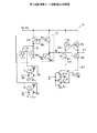
図19には、本実施の形態におけるレベル変換回路45を示している。
(Tenth embodiment)
The tenth embodiment embodying the present invention will be described below.
FIG. 19 shows a
このレベル変換回路45は、電流制限のための高耐圧のPMOSトランジスタPH40,PH41と、該各トランジスタPH40,PH41にバイアス電位PBを供給するバイアス回路46を備える点が図25に示す従来例と相違する。図19において、図25の従来例と同様の構成(各MOSトランジスタPH1,PH2,NH1,NH2やインバータ回路3,4など)については同一の符号を付している。
This
図25のレベル変換回路1の説明で述べたように、出力信号OUTをHレベルからLレベルに変化させるためには、PMOSトランジスタPH2の電流よりもNMOSトランジスタNH2の電流を大きくすることが必要となる。PMOSトランジスタPH2のゲート・ソース間は5V(電源電圧Vpp)であるのに対して、NMOSトランジスタNH2のゲート・ソース間は1.8V(電源電圧Vdd)しかない。PMOSトランジスタPH2の電流よりもNMOSトランジスタNH2の電流を大きくするためには、NMOSトランジスタNH2のゲート幅Wを(トランジスタPH2のゲート幅に対して)大きく設計しなければならず、NMOSトランジスタNH2のサイズが大きくなってしまう。また、電源電圧Vddの電圧値がNMOSトランジスタNH1,NH2のしきい値電圧Vth付近まで下がってくると、遅延時間が極端に大きくなる。これは、NMOSトランジスタNH1,NH2のゲート幅Wを大きくしたとしても、出力信号OUTの出力端子の放電に寄与するPMOSトランジスタPH2とNMOSトランジスタNH2の電流差が小さくなるためである。
As described in the description of the
この問題点を解決するため、本実施の形態のレベル変換回路45では、クロスカップルした高耐圧のPMOSトランジスタPH1,PH2と直列に、電流制限のためのPMOSトランジスタPH40,PH41を設けている。各PMOSトランジスタPH40,PH41のゲートには、バイアス回路46で発生したバイアス電位PBを供給し、各PMOSトランジスタPH40,PH41、つまり、各PMOSトランジスタPH1,PH2に流れる電流を制御する。各PMOSトランジスタPH40,PH41,PH1,PH2に流れる電流の値は、高耐圧のNMOSトランジスタNH1,NH2のゲートに電源電圧Vddが加わったときに流れる電流に比例するように設定する。
In order to solve this problem, in the
具体的には、バイアス回路46は、高耐圧のPMOSトランジスタPH42とNMOSトランジスタNH40と容量C2を含む。PMOSトランジスタPH42のソースには電源電圧Vppが供給され、そのPMOSトランジスタPH42のゲートは、各MOSトランジスタPH42,NH40のドレインに接続されるとともに、容量C2を介して電源電圧Vppの電源に接続される。この容量C2は、バイアス回路46(PMOSトランジスタPH42のゲート)から出力されるバイアス電位PBの安定化容量として働く。
Specifically, the
NMOSトランジスタNH40のソースはグランドに接続され、NMOSトランジスタNH40のゲートには、インバータ回路12から出力される制御信号ENが供給される。また、PMOSトランジスタPH42のゲートが、電流制限用の各PMOSトランジスタPH40,PH41のゲートに接続されている。
The source of the NMOS transistor NH40 is connected to the ground, and the control signal EN output from the
このような回路構成とすると、各PMOSトランジスタPH40,PH41,PH1,PH2に流れる電流の値は、高耐圧のNMOSトランジスタNH1,NH2のゲートに電源電圧Vddが加わったときに流れる電流に比例する。つまり、電源電圧Vddが下がり、NMOSトランジスタNH1,NH2の電流が減少すると、バイアス回路46のNMOSトランジスタNH40に流れる電流も減少する。NMOSトランジスタNH40に流れる電流が減少するので、PMOSトランジスタPH42に流れる電流が減少する。従って、各PMOSトランジスタPH40,PH41,PH1,PH2に流れる電流は、NMOSトランジスタNH1,NH2の電流に比例する特性を得ることができる。このような回路特性とすると、電源電圧Vddが減少しても、PMOSトランジスタPH2の電流よりもNMOSトランジスタNH2の電流を常に大きくすることができる。
With such a circuit configuration, the value of the current flowing through each of the PMOS transistors PH40, PH41, PH1, and PH2 is proportional to the current that flows when the power supply voltage Vdd is applied to the gates of the high breakdown voltage NMOS transistors NH1 and NH2. That is, when the power supply voltage Vdd decreases and the currents of the NMOS transistors NH1 and NH2 decrease, the current flowing through the NMOS transistor NH40 of the
また、制御信号ENをLレベルとすると、NMOSトランジスタNH40がオフしてバイアス回路46に流れる電流を停止することができる。このとき、PMOSトランジスタPH40,PH41もオフしてしまうので、出力信号OUTの信号レベルが不定になる可能性がある。従って、レベル変換回路45の出力信号OUTを受ける回路側には、制御信号との論理機能を設けることで出力信号OUTが不定、或いは中間電位でも該回路に貫通電流が流れないように工夫する。
Further, when the control signal EN is set to the L level, the NMOS transistor NH40 is turned off and the current flowing through the
なお、本実施の形態において、電流制限用のPMOSトランジスタPH40,PH41を、PMOSトランジスタPH1,PH2のソース側に挿入する例を示したが、PMOSトランジスタPH1,PH2のドレイン側に設けて電流を制限するように構成してもよい。 In the present embodiment, the current limiting PMOS transistors PH40 and PH41 are inserted on the source side of the PMOS transistors PH1 and PH2. However, the current limiting PMOS transistors PH40 and PH41 are provided on the drain side of the PMOS transistors PH1 and PH2. You may comprise.
(第11の実施の形態)
以下、本発明を具体化した第11の実施の形態を説明する。
図20には、本実施の形態のレベル変換回路48を示している。このレベル変換回路48は、バイアス回路49とそれを制御する回路(レベル変換回路50を含む回路)部分の構成が上記第10の実施の形態におけるレベル変換回路45と相違する。図20において、第10の実施の形態と同様の構成については同一の符号を付してその説明を一部省略し、以下には、その相違点を中心に説明する。
(Eleventh embodiment)
Hereinafter, an eleventh embodiment embodying the present invention will be described.
FIG. 20 shows the
第10の実施の形態では、NMOSトランジスタNH40がオフしたとき、バイアス回路46に流れる電流を停止することができたが、それと同時にPMOSトランジスタPH40,PH41がオフして出力がハイインピーダンス(出力信号OUTが不定)になる可能性がある。そこで、本実施の形態のレベル変換回路48では、バイアス回路49の電流を停止したときでも、出力がハイインピーダンスとならないような工夫がなされている。
In the tenth embodiment, when the NMOS transistor NH40 is turned off, the current flowing through the
具体的には、バイアス回路49は、上記バイアス回路46を構成するPMOSトランジスタPH42、NMOSトランジスタNH40、容量C2に加え、PMOSトランジスタPH43とNMOSトランジスタNH41とを備える。PMOSトランジスタPH43のソースには5Vの電源電圧Vppが供給され、PMOSトランジスタPH43のドレインがPMOSトランジスタPH42のソースに接続されている。また、NMOSトランジスタNH41のドレインは、PMOSトランジスタPH42のゲートに接続され、NMOSトランジスタNH41のソースがグランドに接続されている。そして、PMOSトランジスタPH43とNMOSトランジスタNH41とのゲートには、レベル変換回路50の出力信号(5Vの制御信号)ENXHが供給される。レベル変換回路50は、PMOSトランジスタPH44,PH45とNMOSトランジスタNH42,NH43、及びインバータ回路51,52で構成される。
Specifically, the
制御信号ENがHレベル(1.8V)であるとき、PMOSトランジスタPL40とNMOSトランジスタNL40からなるインバータ回路51の出力ノードN12はLレベル(0V)となり、PMOSトランジスタPL41とNMOSトランジスタNL41からなるインバータ回路52の出力ノードN13はHレベル(1.8V)となる。このとき、NMOSトランジスタNH43とPMOSトランジスタPH44がオンし、NMOSトランジスタNH42とPMOSトランジスタPH45がオフするため、レベル変換回路50はLレベル(0V)の制御信号ENXHを出力する。
When the control signal EN is at the H level (1.8V), the output node N12 of the
制御信号ENXHがLレベルであるので、NMOSトランジスタNH41はオフし、PMOSトランジスタPH43がオンする。このため、制御信号ENXHがLレベルである場合は、図19のバイアス回路46と同様の動作をする。この場合、ノードN13がHレベルであるので、NMOSトランジスタNH40に電流が流れ、その電流は、バイアス回路46と同じく、高耐圧のNMOSトランジスタNH1,NH2のゲートに電源電圧Vddが加わったときに流れる電流に比例するように設計できる。また、各PMOSトランジスタPH40,PH41,PH1,PH2に流れる電流も同様に、NMOSトランジスタNH1,NH2の電流に比例するように設計できる。
Since the control signal ENXH is at the L level, the NMOS transistor NH41 is turned off and the PMOS transistor PH43 is turned on. Therefore, when the control signal ENXH is at the L level, the operation is the same as that of the
一方、制御信号ENがLレベル(0V)であるとき、インバータ回路51の出力ノードN12はHレベル(1.8V)となり、インバータ回路52の出力ノードN13はLレベル(0V)となる。このとき、NMOSトランジスタNH42とPMOSトランジスタPH45がオンし、NMOSトランジスタNH43とPMOSトランジスタPH44がオフするため、レベル変換回路50はHレベル(5V)の制御信号ENXHを出力する。
On the other hand, when the control signal EN is at L level (0V), the output node N12 of the
制御信号ENXHがHレベルであるので、NMOSトランジスタNH41はオンし、PMOSトランジスタPH43がオフする。PMOSトランジスタPH43がオフすると、バイアス回路49には定常電流は流れなくなる。またこのとき、NMOSトランジスタNH41がオンすることで、バイアス電位PBはグランド電位の0Vとなり、電流制限用のPMOSトランジスタPH40,PH41はオンした状態となる。PMOSトランジスタPH40,PH41のゲートに供給されるバイアス電位PBが0Vとなる場合、信号変化時に、PMOSトランジスタPH40,PH41に流れる電流がNMOSトランジスタNH1,NH2の電流に比例する特性にならないが、入力信号INと出力信号OUTが変化しなければ、以前の状態を保持することができる。従って、レベル変換回路48の入出力信号が変化しない待機時に、バイアス回路49に流れる電流を停止することができる。
Since the control signal ENXH is at the H level, the NMOS transistor NH41 is turned on and the PMOS transistor PH43 is turned off. When the PMOS transistor PH43 is turned off, no steady current flows through the
本実施の形態では、1.8Vの制御信号ENから5Vの制御信号ENXHを発生するのに、図25の従来例と同じ構成のレベル変換回路50を用いている。電源電圧Vddが小さくなると、制御信号ENをレベル変換した制御信号ENXHの遅延時間が大きくなるが、制御信号なので、その遅延時間が多少大きくなっても回路動作には問題はない。なお、このような場合、レベル変換回路50において、PMOSトランジスタPH44,PH45のオン抵抗をできるだけ大きくして、面積を節約しつつ、NMOSトランジスタNH42,NH43のゲート幅Wを大きくして、その動作電圧の下限値をできるだけ下げるように設計すればよい。
In this embodiment, the
このようにレベル変換回路48を構成することで、PMOSトランジスタPH40,PH41,PH1,PH2に流れる電流値を、高耐圧のNMOSトランジスタNH1,NH2のゲートに電源電圧Vddが加わったときに流れる電流に比例するよう制御しながら、待機時に流れるバイアス回路49の電流を停止することが可能となる。
By configuring the
(第12の実施の形態)
以下、本発明を具体化した第12の実施の形態を説明する。
図21は、本実施の形態のレベル変換回路55を示している。このレベル変換回路55は、第1の実施の形態のレベル変換回路10(図5参照)と第10の実施の形態のレベル変換回路45(図19参照)とを組み合わせた回路構成となっている。レベル変換回路55では、それらを組み合わせたことで、バイアス回路46におけるバイアス電位PBの発生方法が相違する。図21において、第1及び第10の実施の形態と同様の構成については同一の符号を付してその説明を一部省略し、以下には、相違点を中心に説明する。
(Twelfth embodiment)
The twelfth embodiment embodying the present invention will be described below.
FIG. 21 shows the
すなわち、レベル変換回路55において、バイアス回路46のNMOSトランジスタNH40のゲートには、バイアス回路11で発生されたバイアス電位NBが供給され、NMOSトランジスタNH40のソースは、PMOSトランジスタPL42とNMOSトランジスタNL42からなるインバータ回路57の出力ノードN40に接続されている。インバータ回路57には、インバータ回路12から出力される制御信号ENが入力され、出力ノードN40の電位は、制御信号ENの論理レベルを反転したレベルとなる。
That is, in the
図19のレベル変換回路45では、信号の変化時に、高耐圧のNMOSトランジスタNH1,NH2に流れる電流は、そのゲートに電源電圧Vddが加わったときに流れる電流値となっていた。そのため、レベル変換回路45では、PMOSトランジスタPH40,PH41,PH1,PH2に流れる電流の値を、NMOSトランジスタNH1,NH2のゲートに電源電圧Vddが加わったときに流れる電流に比例するように制御していた。
In the
これに対し、図21に示す本実施の形態のレベル変換回路55では、信号の変化時に、NMOSトランジスタNH1,NH2のゲートには、電源電圧Vdd+しきい値電圧Vthが加わり、そのゲート電圧に応じた電流がNMOSトランジスタNH1,NH2に流れる。従って、PMOSトランジスタPH40,PH41,PH1,PH2に流れる電流の値は、NMOSトランジスタNH1,NH2のゲートに電源電圧Vdd+しきい値電圧Vthが加わったときに流れる電流に比例するよう制御することが望ましい。
On the other hand, in the
このため、バイアス回路46において、バイアス電位PBを発生するダイオード接続されたPMOSトランジスタPH42に流れる電流は、NMOSトランジスタNH1,NH2のゲートに電源電圧Vdd+しきい値電圧Vthが加わったときに流れる電流に比例するように回路が構成されている。
Therefore, in the
具体的には、図19のレベル変換回路45では、バイアス回路46におけるNMOSトランジスタNH40のソースはグランドGND、NMOSトランジスタNH40のゲート電位は(バイアス回路46の動作時には)電源電圧Vddとしていた。本実施の形態のレベル変換回路55においては、NMOSトランジスタNH40のゲート電位をバイアス電位NB、つまり、電源電圧Vdd+しきい値電圧Vthとしている。また、NMOSトランジスタNH40のソースは、NMOSトランジスタNL42を通してグランドGNDに接続される。これは、NMOSトランジスタNH1,NH2とNMOSトランジスタNL1,NL2のレプリカ回路として働く。
Specifically, in the
このレベル変換回路55において、Hレベルの制御信号ENが供給されると、インバータ回路57の出力ノードN40の電位がLレベル(ほぼ0V)となるので、NMOSトランジスタNH40のゲート・ソース間には、ほぼ電源電圧Vth+しきい値電圧Vthの電圧が加わる。このとき、バイアス回路46において、NMOSトランジスタNH40がオンしてPMOSトランジスタPH42に電流が流れて、バイアス電位PBが発生するため、各PMOSトランジスタPH40,PH41,PH1,PH2に流れる電流の値は、NMOSトランジスタNH1,NH2のゲートに電源電圧Vdd+しきい値電圧Vthが加わったときに流れる電流に比例するようになる。
In this
このように、本実施の形態によれば、上記第1の実施の形態と同様に、バイアス回路11で発生するバイアス電位NBを、電源電圧Vddよりもしきい値電圧Vth高い電圧(2.6V)とすることで、回路動作の高速化が実現できる。さらに、第10の実施の形態と同様に、電源電圧Vddが減少しても、PMOSトランジスタPH2の電流よりもNMOSトランジスタNH2の電流を常に大きくすることができる。
Thus, according to the present embodiment, as in the first embodiment, the bias potential NB generated in the
(第13の実施の形態)
以下、本発明を具体化した第13の実施の形態を説明する。
図22は、本実施の形態のレベル変換回路61を示している。このレベル変換回路61は、第1の実施の形態のレベル変換回路10(図5参照)と第11の実施の形態のレベル変換回路48(図20参照)とを組み合わせた回路構成となっている。図22において、第1及び第11の実施の形態と同様の構成については同一の符号を付している。
(Thirteenth embodiment)
A thirteenth embodiment embodying the present invention will be described below.
FIG. 22 shows the
このレベル変換回路61は、第11の実施の形態と同様に、バイアス回路49のバイアス電流を停止しても、出力信号OUTが不定とならないように回路を構成している。すなわち、レベル変換回路61は、上記第12の実施の形態におけるレベル変換回路55に対して、バイアス回路49のMOSトランジスタPH43,NH41を追加するとともに、レベル変換回路50を追加している。
As in the eleventh embodiment, the
このレベル変換回路61でも、上記第12の実施の形態と同様に、PMOSトランジスタPH40,PH41,PH1,PH2に流れる電流値を、高耐圧のNMOSトランジスタNH1,NH2のゲートに電源電圧Vdd+しきい値電圧Vthが加わったときに流れる電流に比例するよう制御しながら、待機時に流れるバイアス回路49の電流を停止することが可能となる。
In this
(第14の実施の形態)
以下、本発明を具体化した第14の実施の形態を説明する。
図23に示すように、本実施の形態は、1.8Vの制御信号ENから5Vの制御信号ENXHを発生するレベル変換回路62の構成が上記第13の実施の形態と相違する。図23において、第13の実施の形態と同様の構成については同一の符号を付してその説明を一部省略し、以下には、相違点を中心に説明する。
(Fourteenth embodiment)
The fourteenth embodiment embodying the present invention will be described below.
As shown in FIG. 23, the present embodiment is different from the thirteenth embodiment in the configuration of a
レベル変換回路62において、NMOSトランジスタNH42,NH43のゲートにバイアス回路11で発生したバイアス電位(=Vdd+Vth)が供給されている。NMOSトランジスタNH42のソースは、低耐圧のNMOSトランジスタNL42を介してグランドに接続され、NMOSトランジスタNH43のソースは、低耐圧のNMOSトランジスタNL43を介してグランドに接続されている。また、NMOSトランジスタNL42のゲートはインバータ回路51の出力ノードN12に接続され、制御信号ENを反転した電位レベルが供給される。さらに、NMOSトランジスタNL43のゲートはインバータ回路52の出力ノードN13に接続され、制御信号ENと同じレベルが供給される。
In the
バイアス回路49の電流を停止した後、制御信号ENXHを発生するレベル変換回路が動作しなくなる電圧値まで電源電圧Vddが下がると、制御信号ENでバイアス回路49を復帰できなくなるので、バイアス電流を停止できなくなる。
After the current of the
この対策として、本実施の形態のレベル変換回路62では、NMOSトランジスタNH42,NH43のゲート電位をバイアス電位(=Vdd+Vth)とすることで、動作電圧の下限を下げている。すなわち、低い電源電圧Vddの値が小さくなっても、該トランジスタNH42,NH43の電流の減少は、図22のレベル変換回路50と比較して小さくなる。このため、より低い電圧までレベル変換回路62が動作し、1.8V信号である制御信号ENから5Vの制御信号ENXHを確実に発生させることが可能となり、バイアス回路49を制御できる電源電圧Vddの電圧範囲が広くなる。また、制御信号ENでバイアス回路49を制御できる電圧範囲(バイアス回路49を停止した後、制御信号ENで復帰できる電源電圧Vddの電圧範囲)が広くなるので、よりこまめにバイアス回路49を停止することが可能となる。
As a countermeasure against this, in the
また、上記第11の実施の形態において、1.8Vの制御信号ENから5Vの制御信号ENXHを出力するレベル変換回路50の動作電圧の下限を下げるために、PMOSトランジスタPH44,PH45のオン抵抗をできるだけ大きくして、面積を節約しつつ、NMOSトランジスタNH42,NH43のゲート幅Wを大きく設計する方法を説明した。本実施の形態のレベル変換回路62では、その設計方法に加え、NMOSトランジスタNH42,NH43にバイアス電位NB(=Vdd+Vth)が供給されるので、動作電圧の下限をさらに下げることができる。
In the eleventh embodiment, in order to lower the lower limit of the operating voltage of the
(第15の実施の形態)
以下、本発明を具体化した第15の実施の形態を説明する。
図24には、本実施の形態のレベル変換回路71を示している。レベル変換回路71を構成する各MOSトランジスタPH1,PH2,NH1,NH2やインバータ回路3,4の構成は、上記第1の実施の形態と同じであり、バイアス回路72の構成が相違する。
(Fifteenth embodiment)
The fifteenth embodiment embodying the present invention will be described below.
FIG. 24 shows the
バイアス回路72は、前記レベル変換回路62(図23参照)から供給される5Vの制御信号ENXHによって制御される。詳しくは、バイアス回路72は、PMOSトランジスタPH3,NMOSトランジスタNH3、抵抗R6、及び容量C1を含む。バイアス回路72において、PMOSトランジスタPH3のゲートにLレベル(0V)の制御信号ENXHが供給されると、PMOSトランジスタPH3がオンし、抵抗R6を介してNMOSトランジスタNH3にバイアス電流が流れる。一方、PMOSトランジスタPH3のゲートにHレベル(5V)の制御信号ENXHが供給されると、PMOSトランジスタPH3がオフしてバイアス電流が停止される。 The bias circuit 72 is controlled by a 5V control signal ENXH supplied from the level conversion circuit 62 (see FIG. 23). Specifically, the bias circuit 72 includes a PMOS transistor PH3, an NMOS transistor NH3, a resistor R6, and a capacitor C1. In the bias circuit 72, when the control signal ENXH of L level (0V) is supplied to the gate of the PMOS transistor PH3, the PMOS transistor PH3 is turned on, and a bias current flows through the NMOS transistor NH3 via the resistor R6. On the other hand, when the control signal ENXH at the H level (5 V) is supplied to the gate of the PMOS transistor PH3, the PMOS transistor PH3 is turned off and the bias current is stopped.
5Vの制御信号ENXHは、図23のレベル変換回路62において1.8Vの制御信号ENに基づいて生成することができる。よって、本実施の形態においても、上記第1の実施の形態と同様の効果を得ることができる。
The control signal ENXH of 5V can be generated based on the control signal EN of 1.8V in the
尚、上記各実施の形態は、以下の態様で実施してもよい。
・第2の実施の形態のAD変換回路15は、第1の実施の形態のレベル変換回路10を用いるものであったが、このレベル変換回路10に代えて他の実施の形態のレベル変換回路を用いてもよい。また、各実施の形態におけるレベル変換回路は、AD変換回路以外の他の半導体集積回路装置に使用してもよい。
In addition, you may implement each said embodiment in the following aspects.
The
・上記第9の実施の形態におけるパワーオンリセット回路44を他の実施の形態のレベル変換回路に設けてもよい。また、パワーオンリセット回路44はPMOSトランジスタPH31、抵抗RPOR、及び容量CPORにより構成されるものであるが、その回路構成は適宜変更してもよい。
The power-on
上記各実施の形態から把握できる技術的思想を以下に記載する。
(付記1)基準電圧と第1電圧とを信号レベルとする入力信号を、前記基準電圧と第1電圧よりも高い第2電圧の信号レベルに変換するレベル変換回路であって、
第1及び第2のPMOSトランジスタと、第1〜第4のNMOSトランジスタと、バイアス電位を発生するバイアス回路とを含み、
第1のNMOSトランジスタは、ドレインが第1のPMOSトランジスタのドレインと第2のPMOSトランジスタのゲートに接続され、ソースが第3のNMOSトランジスタのドレインに接続され、第2のNMOSトランジスタは、ドレインが第2のPMOSトランジスタのドレインと第1のPMOSトランジスタのゲートに接続され、ソースが第4のNMOSトランジスタのドレインに接続され、第3のNMOSトランジスタのゲートに前記入力信号が供給されるとともに、第4のNMOSトランジスタのゲートに入力信号を反転した信号が供給され、
前記バイアス回路は、前記第1電圧より前記第1及び第2のNMOSトランジスタのしきい値電圧高いバイアス電位を前記第1及び第2のNMOSトランジスタのゲートに供給する回路であり、前記基準電圧と第1電圧とを信号レベルとする制御信号に基づいて前記バイアス電位を発生させるための電流を制御することを特徴とするレベル変換回路。
(付記2)基準電圧と第1電圧とを信号レベルとする入力信号を、前記基準電圧と第1電圧よりも高い第2電圧の信号レベルに変換するレベル変換回路であって、
第1〜第4のPMOSトランジスタと、第1及び第2のNMOSトランジスタと、バイアス電位を発生するバイアス回路とを含み、
第1のNMOSトランジスタのドレインは、第1のPMOSトランジスタのドレインと第2のPMOSトランジスタのゲートに接続され、第2のNMOSトランジスタのドレインは、第2のPMOSトランジスタのドレインと第1のPMOSトランジスタのゲートに接続され、第3のPMOSトランジスタのドレインは、前記第1のPMOSトランジスタのソースに接続され、第4のPMOSトランジスタのドレインは、前記第2のPMOSトランジスタのソースに接続され、
前記バイアス回路は、前記第3及び第4のPMOSトランジスタのゲートに前記バイアス電位を供給し、出力信号の変化時に第3及び第4のPMOSトランジスタに流れる電流が第1及び第2のNMOSトランジスタに流れる電流と比例関係となるよう制御することを特徴とするレベル変換回路。
(付記3)基準電圧と第1電圧とを信号レベルとする入力信号を、前記基準電圧と第1電圧よりも高い第2電圧の信号レベルに変換するレベル変換回路であって、
第1〜第4のPMOSトランジスタと、第1〜第4のNMOSトランジスタと、第1のバイアス電位を発生する第1のバイアス回路と、第2のバイアス電位を発生する第2のバイアス回路とを含み、
第1のNMOSトランジスタは、ドレインが第1のPMOSトランジスタのドレインと第2のPMOSトランジスタのゲートに接続され、ソースが第3のNMOSトランジスタのドレインに接続され、第2のNMOSトランジスタは、ドレインが第2のPMOSトランジスタのドレインと第1のPMOSトランジスタのゲートに接続され、ソースが第4のNMOSトランジスタのドレインに接続され、第3のPMOSトランジスタのドレインは、第1のPMOSトランジスタのソースに接続され、第4のPMOSトランジスタのドレインは、第2のPMOSトランジスタのソースに接続され、
第3のNMOSトランジスタのゲートに前記入力信号が供給されるとともに、第4のNMOSトランジスタのゲートに入力信号を反転した信号が供給され、
前記第1のバイアス回路は、前記第1電圧より前記第1及び第2のNMOSトランジスタのしきい値電圧高い第1のバイアス電位を前記第1及び第2のNMOSトランジスタのゲートに供給する回路であり、前記基準電圧と第1電圧とを信号レベルとする制御信号に基づいて、前記第1のバイアス電位を発生させるための電流を制御し、
前記第2のバイアス回路は、前記第3及び第4のPMOSトランジスタのゲートに前記第2のバイアス電位を供給し、出力信号の変化時に第3及び第4のPMOSトランジスタに流れる電流が第1及び第2のNMOSトランジスタに流れる電流と比例関係となるよう制御することを特徴とするレベル変換回路。
(付記4)前記バイアス回路は、バイアス電流を設定するための抵抗と、前記制御信号に基づいて前記抵抗に流れる電流を制御するMOSトランジスタとを備えることを特徴とする付記1に記載のレベル変換回路。
(付記5)前記バイアス回路は、前記バイアス電流を設定するための抵抗を複数備えることを特徴とする付記4に記載のレベル変換回路。
(付記6)前記第2電圧の立ち上がりを検出して前記バイアス回路にリセット信号を供給するパワーオンリセット回路を備え、前記バイアス回路は、そのリセット信号に基づいてバイアス電流を増加させることを特徴とする付記1に記載のレベル変換回路。
(付記7)前記バイアス回路は、バイアス電流の停止時にバイアス電位を前記基準電圧の電位レベルとするためのMOSトランジスタを備えることを特徴とする付記2に記載のレベル変換回路。
(付記8)前記バイアス回路は、前記バイアス電位を安定化するための容量を備えることを特徴とすることを特徴とする付記1〜7のいずれかに記載のレベル変換回路。
(付記9)前記バイアス回路は、複数のMOSトランジスタからなる自己バイアス回路が出力するバイアス電位に基づいてバイアス電流を決定することを特徴とする付記1に記載のレベル変換回路。
(付記10)前記バイアス回路は、前記第2電圧の電源に接続されカレントミラー回路を構成する一対のPMOSトランジスタと、ドレインとゲートが前記ミラー回路に接続されるとともにソースが前記第1電圧の電源に接続されるNMOSトランジスタとを備えることを特徴とする付記1に記載のレベル変換回路。
(付記11)前記バイアス回路は、前記カレントミラー回路に流れるバイアス電流を設定するための抵抗と、前記制御信号に基づいて前記抵抗に流れる電流を制御するNMOSトランジスタとを備えることを特徴とする付記10に記載のレベル変換回路。
(付記12)前記各MOSトランジスタからなる変換部を複数備え、該各変換部にバイアス電位を供給するバイアス回路を共通に用いるようにしたことを特徴とする付記1に記載のレベル変換回路。
(付記13)基準電圧と第1電圧との電圧レベルの入力信号を、前記基準電圧と前記第1電圧よりも高い第2電圧との電圧レベルの出力信号にレベル変換するレベル変換回路であって、
バイアス電位を発生するバイアス回路と、クロスカップルされた第1及び第2のPMOSトランジスタと、該各PMOSトランジスタに直列に接続され、ゲートに前記バイアス電位が供給される第1及び第2のNMOSトランジスタと、前記各NMOSトランジスタに直列に接続され、ゲートに前記入力信号が供給される第3及び第4のNMOSトランジスタと、を含み、
前記バイアス電位は、前記第1電圧より前記第1及び第2のNMOSトランジスタのしきい値電圧高い電位であり、前記バイアス回路は、前記基準電圧と第1電圧とを信号レベルとする制御信号に基づいて前記バイアス電位を発生させるための電流を制御することを特徴とするレベル変換回路。
(付記14)基準電圧と第1電圧との電圧レベルの入力信号を、前記基準電圧と前記第1電圧よりも高い第2電圧との電圧レベルの出力信号にレベル変換するレベル変換回路であって、
バイアス電位を発生するバイアス回路と、クロスカップルされた第1及び第2のPMOSトランジスタと、該各PMOSトランジスタと直列に接続され、ゲートに供給される前記バイアス電位に基づいて前記各PMOSトランジスタに流れる電流を制限する第3及び第4のPMOSトランジスタと、前記PMOSトランジスタと直列に接続され、ゲートに前記入力信号が供給される第1及び第2のNチャネルMOSトランジスタと、を含み、
前記バイアス回路は、前記バイアス電位に基づいて、出力信号の変化時に第3及び第4のPMOSトランジスタに流れる電流が第1及び第2のNMOSトランジスタに流れる電流と比例関係となるよう制御することを特徴とするレベル変換回路。
(付記15)付記1〜14のいずれかに記載のレベル変換回路と、該レベル変換回路を制御する制御回路とを含むことを特徴とする半導体集積回路装置。
(付記16)アナログ信号からデジタル信号に変換するAD変換を行うことを特徴とする付記15に記載の半導体集積回路装置。
The technical ideas that can be grasped from the above embodiments are described below.
(Appendix 1) A level conversion circuit for converting an input signal having a reference voltage and a first voltage as signal levels into a signal level of a second voltage higher than the reference voltage and the first voltage,
Including first and second PMOS transistors, first to fourth NMOS transistors, and a bias circuit for generating a bias potential;
The drain of the first NMOS transistor is connected to the drain of the first PMOS transistor and the gate of the second PMOS transistor, the source is connected to the drain of the third NMOS transistor, and the drain of the second NMOS transistor The drain of the second PMOS transistor and the gate of the first PMOS transistor are connected, the source is connected to the drain of the fourth NMOS transistor, the input signal is supplied to the gate of the third NMOS transistor, and the first The signal obtained by inverting the input signal is supplied to the gate of the NMOS transistor No. 4,
The bias circuit is a circuit that supplies a bias potential higher than a threshold voltage of the first and second NMOS transistors to the gates of the first and second NMOS transistors than the first voltage; A level conversion circuit for controlling a current for generating the bias potential based on a control signal having a signal level of a first voltage.
(Supplementary note 2) A level conversion circuit for converting an input signal having a signal level of a reference voltage and a first voltage into a signal level of a second voltage higher than the reference voltage and the first voltage,
Including first to fourth PMOS transistors, first and second NMOS transistors, and a bias circuit for generating a bias potential;
The drain of the first NMOS transistor is connected to the drain of the first PMOS transistor and the gate of the second PMOS transistor, and the drain of the second NMOS transistor is the drain of the second PMOS transistor and the first PMOS transistor. The drain of the third PMOS transistor is connected to the source of the first PMOS transistor, the drain of the fourth PMOS transistor is connected to the source of the second PMOS transistor,
The bias circuit supplies the bias potential to the gates of the third and fourth PMOS transistors, and a current flowing through the third and fourth PMOS transistors when the output signal changes changes to the first and second NMOS transistors. A level conversion circuit which is controlled so as to be proportional to a flowing current.
(Supplementary note 3) A level conversion circuit for converting an input signal having a reference voltage and a first voltage as signal levels into a signal level of a second voltage higher than the reference voltage and the first voltage,
First to fourth PMOS transistors, first to fourth NMOS transistors, a first bias circuit for generating a first bias potential, and a second bias circuit for generating a second bias potential Including
The drain of the first NMOS transistor is connected to the drain of the first PMOS transistor and the gate of the second PMOS transistor, the source is connected to the drain of the third NMOS transistor, and the drain of the second NMOS transistor The drain of the second PMOS transistor is connected to the gate of the first PMOS transistor, the source is connected to the drain of the fourth NMOS transistor, and the drain of the third PMOS transistor is connected to the source of the first PMOS transistor. The drain of the fourth PMOS transistor is connected to the source of the second PMOS transistor;
The input signal is supplied to the gate of the third NMOS transistor, and the signal obtained by inverting the input signal is supplied to the gate of the fourth NMOS transistor.
The first bias circuit is a circuit for supplying a first bias potential higher than a threshold voltage of the first and second NMOS transistors to the gates of the first and second NMOS transistors than the first voltage. And, based on a control signal having a signal level of the reference voltage and the first voltage, controlling a current for generating the first bias potential,
The second bias circuit supplies the second bias potential to the gates of the third and fourth PMOS transistors, and currents flowing through the third and fourth PMOS transistors when the output signal changes are the first and fourth PMOS transistors. A level conversion circuit, characterized in that the level conversion circuit is controlled so as to be proportional to a current flowing through the second NMOS transistor.
(Supplementary note 4) The level conversion according to
(Supplementary Note 5) The level conversion circuit according to
(Appendix 6) A power-on reset circuit that detects a rising edge of the second voltage and supplies a reset signal to the bias circuit, wherein the bias circuit increases a bias current based on the reset signal. The level conversion circuit according to
(Supplementary note 7) The level conversion circuit according to
(Additional remark 8) The said bias circuit is provided with the capacity | capacitance for stabilizing the said bias potential, The level conversion circuit in any one of Additional remark 1-7 characterized by the above-mentioned.
(Supplementary note 9) The level conversion circuit according to
(Supplementary Note 10) The bias circuit includes a pair of PMOS transistors that are connected to the power source of the second voltage to form a current mirror circuit, a drain and a gate are connected to the mirror circuit, and a source is the power source of the first voltage The level conversion circuit according to
(Additional remark 11) The said bias circuit is provided with the resistance for setting the bias current which flows into the said current mirror circuit, and the NMOS transistor which controls the electric current which flows into the said resistance based on the said control signal. The level conversion circuit according to 10.
(Supplementary note 12) The level conversion circuit according to
(Supplementary note 13) A level conversion circuit for level-converting an input signal having a voltage level of a reference voltage and a first voltage into an output signal having a voltage level of the reference voltage and a second voltage higher than the first voltage. ,
Bias circuit for generating a bias potential, cross-coupled first and second PMOS transistors, and first and second NMOS transistors connected in series to each PMOS transistor and supplied with the bias potential at the gate And third and fourth NMOS transistors connected in series to each of the NMOS transistors and supplied with the input signal at the gate,
The bias potential is a potential higher than the first voltage by the threshold voltages of the first and second NMOS transistors, and the bias circuit generates a control signal having the reference voltage and the first voltage as signal levels. A level conversion circuit that controls a current for generating the bias potential based on the level conversion circuit.
(Supplementary note 14) A level conversion circuit for level-converting an input signal having a voltage level of a reference voltage and a first voltage into an output signal having a voltage level of the reference voltage and a second voltage higher than the first voltage. ,
A bias circuit for generating a bias potential, cross-coupled first and second PMOS transistors, and each PMOS transistor connected in series and flowing to each PMOS transistor based on the bias potential supplied to the gate Third and fourth PMOS transistors for limiting current; and first and second N-channel MOS transistors connected in series with the PMOS transistor and supplied with the input signal at a gate;
The bias circuit controls based on the bias potential so that a current flowing through the third and fourth PMOS transistors is proportional to a current flowing through the first and second NMOS transistors when the output signal changes. A characteristic level conversion circuit.
(Supplementary note 15) A semiconductor integrated circuit device comprising the level conversion circuit according to any one of
(Supplementary note 16) The semiconductor integrated circuit device according to
10,22,27,28,30,35,40 レベル変換回路
43,45,48,55,61,71 レベル変換回路
11,23,31,41,46,49,72 バイアス回路
15 半導体集積回路装置としてのAD変換回路
18 逐次比較制御回路
44 パワーオンリセット回路
C1,C2 容量
IN,IN1,IN2 入力信号
EN,ENX,PD,PDX 制御信号
NB バイアス電位
NH1 第1のNMOSトランジスタ
NH2 第2のNMOSトランジスタ
NH4,NH41 MOSトランジスタ
NL1 第3のNMOSトランジスタ
NL2 第4のNMOSトランジスタ
OUT,OUT1,OUT2 出力信号
PB バイアス電位
PH1 第1のPMOSトランジスタ
PH2 第2のPMOSトランジスタ
PH40 第3のPMOSトランジスタ
PH41 第4のPMOSトランジスタ
R1,R3 抵抗
Vdd 第1電圧としての電源電圧
Vin アナログ信号
Vth しきい値電圧
Vpp 第2電圧としての電源電圧
10, 22, 27, 28, 30, 35, 40
Claims (10)
第1及び第2のPMOSトランジスタと、第1〜第4のNMOSトランジスタと、バイアス電位を発生するバイアス回路とを含み、
第1のNMOSトランジスタは、ドレインが第1のPMOSトランジスタのドレインと第2のPMOSトランジスタのゲートに接続され、ソースが第3のNMOSトランジスタのドレインに接続され、第2のNMOSトランジスタは、ドレインが第2のPMOSトランジスタのドレインと第1のPMOSトランジスタのゲートに接続され、ソースが第4のNMOSトランジスタのドレインに接続され、第3のNMOSトランジスタのゲートに前記入力信号が供給されるとともに、第4のNMOSトランジスタのゲートに入力信号を反転した信号が供給され、
前記バイアス回路は、前記第1電圧より前記第1及び第2のNMOSトランジスタのしきい値電圧高いバイアス電位を前記第1及び第2のNMOSトランジスタのゲートに供給する回路であり、前記基準電圧と第1電圧とを信号レベルとする制御信号に基づいて前記バイアス電位を発生させるための電流を制御し、
前記第2電圧の立ち上がりを検出して前記バイアス回路にリセット信号を供給するパワーオンリセット回路を備え、前記バイアス回路は、そのリセット信号に基づいてバイアス電流を増加させることを特徴とするレベル変換回路。 A level conversion circuit for converting an input signal having a reference voltage and a first voltage as signal levels into a signal level of a second voltage higher than the reference voltage and the first voltage,
Including first and second PMOS transistors, first to fourth NMOS transistors, and a bias circuit for generating a bias potential;
The drain of the first NMOS transistor is connected to the drain of the first PMOS transistor and the gate of the second PMOS transistor, the source is connected to the drain of the third NMOS transistor, and the drain of the second NMOS transistor The drain of the second PMOS transistor and the gate of the first PMOS transistor are connected, the source is connected to the drain of the fourth NMOS transistor, the input signal is supplied to the gate of the third NMOS transistor, and the first The signal obtained by inverting the input signal is supplied to the gate of the NMOS transistor No. 4,
The bias circuit is a circuit that supplies a bias potential higher than a threshold voltage of the first and second NMOS transistors to the gates of the first and second NMOS transistors than the first voltage; Controlling a current for generating the bias potential based on a control signal having a signal level of the first voltage ;
A level conversion circuit comprising a power-on reset circuit that detects a rising edge of the second voltage and supplies a reset signal to the bias circuit, and the bias circuit increases a bias current based on the reset signal. .
第1〜第4のPMOSトランジスタと、第1〜第4のNMOSトランジスタと、第1のバイアス電位を発生する第1のバイアス回路と、第2のバイアス電位を発生する第2のバイアス回路とを含み、 First to fourth PMOS transistors, first to fourth NMOS transistors, a first bias circuit for generating a first bias potential, and a second bias circuit for generating a second bias potential Including
第1のNMOSトランジスタは、ドレインが第1のPMOSトランジスタのドレインと第2のPMOSトランジスタのゲートに接続され、ソースが第3のNMOSトランジスタのドレインに接続され、第2のNMOSトランジスタは、ドレインが第2のPMOSトランジスタのドレインと第1のPMOSトランジスタのゲートに接続され、ソースが第4のNMOSトランジスタのドレインに接続され、第3のPMOSトランジスタのドレインは、第1のPMOSトランジスタのソースに接続され、第4のPMOSトランジスタのドレインは、第2のPMOSトランジスタのソースに接続され、 The drain of the first NMOS transistor is connected to the drain of the first PMOS transistor and the gate of the second PMOS transistor, the source is connected to the drain of the third NMOS transistor, and the drain of the second NMOS transistor The drain of the second PMOS transistor is connected to the gate of the first PMOS transistor, the source is connected to the drain of the fourth NMOS transistor, and the drain of the third PMOS transistor is connected to the source of the first PMOS transistor. The drain of the fourth PMOS transistor is connected to the source of the second PMOS transistor;
第3のNMOSトランジスタのゲートに前記入力信号が供給されるとともに、第4のNMOSトランジスタのゲートに入力信号を反転した信号が供給され、 The input signal is supplied to the gate of the third NMOS transistor, and the signal obtained by inverting the input signal is supplied to the gate of the fourth NMOS transistor.
前記第1のバイアス回路は、前記第1電圧より前記第1及び第2のNMOSトランジスタのしきい値電圧高い第1のバイアス電位を前記第1及び第2のNMOSトランジスタのゲートに供給する回路であり、前記基準電圧と第1電圧とを信号レベルとする制御信号に基づいて、前記第1のバイアス電位を発生させるための電流を制御し、 The first bias circuit is a circuit for supplying a first bias potential higher than a threshold voltage of the first and second NMOS transistors to the gates of the first and second NMOS transistors than the first voltage. And, based on a control signal having a signal level of the reference voltage and the first voltage, controlling a current for generating the first bias potential,
前記第2のバイアス回路は、前記第3及び第4のPMOSトランジスタのゲートに前記第2のバイアス電位を供給し、出力信号の変化時に第3及び第4のPMOSトランジスタに流れる電流が第1及び第2のNMOSトランジスタに流れる電流と比例関係となるよう制御することを特徴とするレベル変換回路。 The second bias circuit supplies the second bias potential to the gates of the third and fourth PMOS transistors, and currents flowing through the third and fourth PMOS transistors when the output signal changes are the first and fourth PMOS transistors. A level conversion circuit, characterized in that the level conversion circuit is controlled so as to be proportional to a current flowing through the second NMOS transistor.
バイアス電位を発生するバイアス回路と、クロスカップルされた第1及び第2のPMOSトランジスタと、該各PMOSトランジスタに直列に接続され、ゲートに前記バイアス電位が供給される第1及び第2のNMOSトランジスタと、前記各NMOSトランジスタに直列に接続され、ゲートに前記入力信号が供給される第3及び第4のNMOSトランジスタと、を含み、 Bias circuit for generating a bias potential, cross-coupled first and second PMOS transistors, and first and second NMOS transistors connected in series to each PMOS transistor and supplied with the bias potential at the gate And third and fourth NMOS transistors connected in series to each of the NMOS transistors and supplied with the input signal at the gate,
前記バイアス電位は、前記第1電圧より前記第1及び第2のNMOSトランジスタのしきい値電圧高い電位であり、前記バイアス回路は、前記基準電圧と第1電圧とを信号レベルとする制御信号に基づいて前記バイアス電位を発生させるための電流を制御し、 The bias potential is a potential higher than the first voltage by the threshold voltages of the first and second NMOS transistors, and the bias circuit generates a control signal having the reference voltage and the first voltage as signal levels. Based on the current to generate the bias potential,
前記第2電圧の立ち上がりを検出して前記バイアス回路にリセット信号を供給するパワーオンリセット回路を備え、前記バイアス回路は、そのリセット信号に基づいてバイアス電流を増加させることを特徴とするレベル変換回路。 A level conversion circuit comprising a power-on reset circuit that detects a rising edge of the second voltage and supplies a reset signal to the bias circuit, and the bias circuit increases a bias current based on the reset signal. .
Priority Applications (3)
| Application Number | Priority Date | Filing Date | Title |
|---|---|---|---|
| JP2004125869A JP4421365B2 (en) | 2004-04-21 | 2004-04-21 | Level conversion circuit |
| US10/948,524 US7176740B2 (en) | 2004-04-21 | 2004-09-24 | Level conversion circuit |
| US11/650,485 US7414453B2 (en) | 2004-04-21 | 2007-01-08 | Level conversion circuit |
Applications Claiming Priority (1)
| Application Number | Priority Date | Filing Date | Title |
|---|---|---|---|
| JP2004125869A JP4421365B2 (en) | 2004-04-21 | 2004-04-21 | Level conversion circuit |
Related Child Applications (1)
| Application Number | Title | Priority Date | Filing Date |
|---|---|---|---|
| JP2009251850A Division JP5045730B2 (en) | 2009-11-02 | 2009-11-02 | Level conversion circuit |
Publications (2)
| Publication Number | Publication Date |
|---|---|
| JP2005311712A JP2005311712A (en) | 2005-11-04 |
| JP4421365B2 true JP4421365B2 (en) | 2010-02-24 |
Family
ID=35135807
Family Applications (1)
| Application Number | Title | Priority Date | Filing Date |
|---|---|---|---|
| JP2004125869A Expired - Lifetime JP4421365B2 (en) | 2004-04-21 | 2004-04-21 | Level conversion circuit |
Country Status (2)
| Country | Link |
|---|---|
| US (2) | US7176740B2 (en) |
| JP (1) | JP4421365B2 (en) |
Families Citing this family (54)
| Publication number | Priority date | Publication date | Assignee | Title |
|---|---|---|---|---|
| US7205820B1 (en) * | 2004-07-08 | 2007-04-17 | Pmc-Sierra, Inc. | Systems and methods for translation of signal levels across voltage domains |
| US7259610B1 (en) * | 2004-09-24 | 2007-08-21 | National Semiconductor Corporation | Static CMOS logic level shift circuit with a low logic input count high switching speed and low power dissipation |
| US7378896B2 (en) * | 2005-05-13 | 2008-05-27 | O2Micro International Ltd. | Single pin for multiple functional control purposes |
| JP5079504B2 (en) * | 2005-06-10 | 2012-11-21 | ティーピーオー、ホンコン、ホールディング、リミテッド | Buffer circuit |
| JP4772480B2 (en) * | 2005-11-30 | 2011-09-14 | 株式会社東芝 | Semiconductor integrated device |
| US7397279B2 (en) * | 2006-01-27 | 2008-07-08 | Agere Systems Inc. | Voltage level translator circuit with wide supply voltage range |
| JP2009526461A (en) * | 2006-02-09 | 2009-07-16 | エヌエックスピー ビー ヴィ | Circuit apparatus and method for detecting power down state of voltage supply |
| US7310012B2 (en) * | 2006-04-19 | 2007-12-18 | Faraday Technology Corp. | Voltage level shifter apparatus |
| JP2007306042A (en) | 2006-05-08 | 2007-11-22 | Sony Corp | Level conversion circuit and input / output apparatus using the same |
| US7498842B2 (en) * | 2006-07-24 | 2009-03-03 | International Business Machines Corporation | High speed voltage level shifter circuits |
| US7362137B2 (en) * | 2006-07-24 | 2008-04-22 | International Business Machines Corporation | High speed voltage level shifter circuits |
| US7834662B2 (en) * | 2006-12-13 | 2010-11-16 | Apple Inc. | Level shifter with embedded logic and low minimum voltage |
| US7652504B2 (en) * | 2006-12-13 | 2010-01-26 | Apple Inc. | Low latency, power-down safe level shifter |
| JP2008211317A (en) * | 2007-02-23 | 2008-09-11 | Fujitsu Ltd | Level shifting circuit |
| US7605633B2 (en) * | 2007-03-20 | 2009-10-20 | Kabushiki Kaisha Toshiba | Level shift circuit which improved the blake down voltage |
| US20090058493A1 (en) * | 2007-08-31 | 2009-03-05 | Matthias Arnold | Signal Level Converter |
| US7446566B1 (en) * | 2007-10-16 | 2008-11-04 | Freescale Semiconductor, Inc. | Level shifter |
| JP5088117B2 (en) * | 2007-12-06 | 2012-12-05 | 富士通株式会社 | Level shifter circuit |
| GB2455432B (en) * | 2007-12-14 | 2013-04-10 | Icera Inc | Voltage control |
| TWI376097B (en) * | 2008-09-18 | 2012-11-01 | Ili Technology Corp | Level shift circuit |
| GB2467183B (en) * | 2009-01-27 | 2013-08-07 | Innovision Res & Tech Plc | Apparatus for use in near field rf communicators |
| JP5198309B2 (en) * | 2009-02-10 | 2013-05-15 | 株式会社東芝 | Level shifter circuit |
| US8102728B2 (en) * | 2009-04-07 | 2012-01-24 | Apple Inc. | Cache optimizations using multiple threshold voltage transistors |
| JP5313779B2 (en) | 2009-06-22 | 2013-10-09 | ルネサスエレクトロニクス株式会社 | Level shift circuit |
| US7995410B2 (en) | 2009-06-26 | 2011-08-09 | Apple Inc. | Leakage and NBTI reduction technique for memory |
| US8018251B1 (en) | 2010-06-01 | 2011-09-13 | Pmc-Sierra, Inc. | Input/output interfacing with low power |
| TWI410048B (en) * | 2010-06-03 | 2013-09-21 | Orise Technology Co Ltd | Level shifter |
| JP5215356B2 (en) * | 2010-07-14 | 2013-06-19 | 株式会社半導体理工学研究センター | Level converter circuit |
| US8207775B2 (en) * | 2010-08-30 | 2012-06-26 | Taiwan Semiconductor Manufacturing Co., Ltd. | VOL up-shifting level shifters |
| JP5581957B2 (en) * | 2010-10-08 | 2014-09-03 | ソニー株式会社 | Level conversion circuit, display device, and electronic device |
| TW201218627A (en) * | 2010-10-20 | 2012-05-01 | Fitipower Integrated Tech Inc | capable of reducing the current consumption of a level shifter during logic transition and downsizing the circuit area of a level shifter |
| CN102457263A (en) * | 2010-11-01 | 2012-05-16 | 天钰科技股份有限公司 | Circuit and method for improving level shifter |
| US8624641B1 (en) | 2010-11-03 | 2014-01-07 | Pmc-Sierra, Inc. | Apparatus and method for driving a transistor |
| US8553488B2 (en) | 2011-06-10 | 2013-10-08 | Apple Inc. | Performing stuck-at testing using multiple isolation circuits |
| US8466722B2 (en) * | 2011-10-28 | 2013-06-18 | International Business Machines Corporation | Startup and protection circuitry for thin oxide output stage |
| US8975942B2 (en) * | 2012-03-01 | 2015-03-10 | Analog Devices, Inc. | System for a clock shifter circuit |
| TWI452568B (en) * | 2012-08-15 | 2014-09-11 | Orise Technology Co Ltd | Latched level shift system |
| CN103812498B (en) * | 2012-11-13 | 2016-10-05 | 台湾积体电路制造股份有限公司 | Over-driving device |
| WO2014142842A1 (en) * | 2013-03-13 | 2014-09-18 | Schneider Electric USA, Inc. | Supply regulation circuit with energy efficient digital control |
| US9337840B2 (en) * | 2013-05-17 | 2016-05-10 | Samsung Electronics Co., Ltd. | Voltage level shifter and systems implementing the same |
| US9463328B2 (en) | 2013-06-11 | 2016-10-11 | Cameron Health, Inc. | Nanopower voltage reference for an implantable medical device |
| JP6088936B2 (en) | 2013-08-07 | 2017-03-01 | ルネサスエレクトロニクス株式会社 | Level shifter |
| JP6298683B2 (en) * | 2014-03-28 | 2018-03-20 | ラピスセミコンダクタ株式会社 | Semiconductor circuit, semiconductor device, and potential supply circuit |
| US9257973B1 (en) * | 2014-11-04 | 2016-02-09 | Texas Instruments Incorporated | Supply-state-enabled level shifter interface circuit and method |
| US9438240B1 (en) * | 2015-08-31 | 2016-09-06 | Cypress Semiconductor Corporation | Biasing circuit for level shifter with isolation |
| US9866205B2 (en) | 2015-11-16 | 2018-01-09 | Taiwan Semiconductor Manufacturing Co., Ltd. | Level conversion device and method |
| US9608633B1 (en) * | 2015-11-24 | 2017-03-28 | Omnivision Technologies, Inc. | Interface circuit with configurable variable supply voltage for transmitting signals |
| US10164798B2 (en) * | 2016-12-05 | 2018-12-25 | Synopsys, Inc. | Driver circuit for transmitter |
| JP2018186400A (en) * | 2017-04-26 | 2018-11-22 | ラピスセミコンダクタ株式会社 | Level shift circuit |
| JP6505815B2 (en) * | 2017-11-17 | 2019-04-24 | ルネサスエレクトロニクス株式会社 | Level shifter |
| US10270448B1 (en) * | 2018-05-16 | 2019-04-23 | Nxp B.V. | Level shifter circuit with transistor drive strength variation compensation |
| US10707845B2 (en) * | 2018-11-13 | 2020-07-07 | Marvell International Ltd. | Ultra-low voltage level shifter |
| CN114326899B (en) * | 2021-12-27 | 2023-09-15 | 上海贝岭股份有限公司 | Integrated circuit and clamping circuit thereof |
| US11736105B1 (en) | 2022-06-02 | 2023-08-22 | Qualcomm Incorporated | Bias current receiver with selective coupling circuit |
Family Cites Families (38)
| Publication number | Priority date | Publication date | Assignee | Title |
|---|---|---|---|---|
| US4717840A (en) * | 1986-03-14 | 1988-01-05 | Western Digital Corporation | Voltage level sensing power-up reset circuit |
| JPH05308274A (en) * | 1992-04-30 | 1993-11-19 | Matsushita Electric Ind Co Ltd | Cmos level shift circuit |
| JPH0637624A (en) | 1992-07-13 | 1994-02-10 | Nec Corp | Level conversion circuit |
| JPH06204850A (en) | 1993-01-07 | 1994-07-22 | Oki Electric Ind Co Ltd | Level shifter circuit |
| US5461333A (en) * | 1993-03-15 | 1995-10-24 | At&T Ipm Corp. | Multi-chip modules having chip-to-chip interconnections with reduced signal voltage level and swing |
| US5631941A (en) * | 1993-06-15 | 1997-05-20 | Yozan Inc. | Register circuit |
| JP3890614B2 (en) | 1995-06-19 | 2007-03-07 | 富士通株式会社 | Boost voltage supply circuit |
| JP3699764B2 (en) * | 1996-01-31 | 2005-09-28 | 株式会社東芝 | Driver circuit device and interface |
| KR100189752B1 (en) * | 1996-06-01 | 1999-06-01 | 구본준 | Power pump circuit with independent well bias voltage |
| KR100228529B1 (en) * | 1996-12-20 | 1999-11-01 | 윤종용 | Level shifter for semiconductor memory |
| JP2993462B2 (en) * | 1997-04-18 | 1999-12-20 | 日本電気株式会社 | Output buffer circuit |
| JP4063982B2 (en) * | 1998-12-04 | 2008-03-19 | 松下電器産業株式会社 | Level shifter circuit and semiconductor device using the same |
| JP2000295089A (en) * | 1999-04-07 | 2000-10-20 | Hitachi Ltd | Output circuit and semiconductor device using the same |
| JP2000353946A (en) * | 1999-06-10 | 2000-12-19 | Matsushita Electric Ind Co Ltd | Level shifter circuit |
| IT1313227B1 (en) * | 1999-07-02 | 2002-06-17 | St Microelectronics Srl | VOLTAGE TRANSLATOR, IN PARTICULAR CMOS TYPE. |
| US6331797B1 (en) * | 1999-11-23 | 2001-12-18 | Philips Electronics North America Corporation | Voltage translator circuit |
| JP2001210076A (en) * | 2000-01-27 | 2001-08-03 | Fujitsu Ltd | Semiconductor integrated circuit, and internal power source voltage generating method for semiconductor integrated circuit |
| JP3699878B2 (en) | 2000-03-27 | 2005-09-28 | 株式会社東芝 | Semiconductor integrated circuit |
| JP3658280B2 (en) * | 2000-06-09 | 2005-06-08 | シャープ株式会社 | Voltage level shifter circuit and nonvolatile semiconductor memory device using the same |
| US6680985B1 (en) * | 2000-08-15 | 2004-01-20 | Hughes Electronics Corporation | Adaptive quadrature amplitude modulation decoding system |
| JP3999460B2 (en) * | 2000-12-22 | 2007-10-31 | 富士通株式会社 | Level shift circuit and semiconductor device |
| US6917239B2 (en) * | 2000-10-24 | 2005-07-12 | Fujitsu Limited | Level shift circuit and semiconductor device |
| KR100370240B1 (en) * | 2000-10-31 | 2003-02-05 | 삼성전자 주식회사 | Current sense amplifier circuit for improving stability and amplification degree in semiconductor memory device |
| JP4048232B2 (en) | 2000-12-27 | 2008-02-20 | 三洋電機株式会社 | Level shift circuit |
| US6791391B2 (en) * | 2001-07-16 | 2004-09-14 | Matsushita Electric Industrial Co., Ltd. | Level shifting circuit |
| JP2003101405A (en) * | 2001-07-16 | 2003-04-04 | Matsushita Electric Ind Co Ltd | Level shifting circuit |
| JP3887189B2 (en) | 2001-08-14 | 2007-02-28 | 株式会社東芝 | Semiconductor integrated circuit |
| JP4327411B2 (en) * | 2001-08-31 | 2009-09-09 | 株式会社ルネサステクノロジ | Semiconductor device |
| US6518818B1 (en) * | 2001-09-17 | 2003-02-11 | Honeywell International Inc. | High voltage CMOS output driver in low voltage process |
| US6534806B1 (en) * | 2001-12-04 | 2003-03-18 | National Semiconductor Corporation | System for generating a reference voltage |
| JP2003198800A (en) | 2001-12-28 | 2003-07-11 | Murata Mach Ltd | Internet facsimile machine |
| JP2003309463A (en) * | 2002-04-15 | 2003-10-31 | Mitsubishi Electric Corp | Level shift circuit |
| KR100521370B1 (en) * | 2003-01-13 | 2005-10-12 | 삼성전자주식회사 | Level shift having power dectection unit to cut off leakage current path |
| US6774698B1 (en) * | 2003-01-30 | 2004-08-10 | Agere Systems Inc. | Voltage translator circuit for a mixed voltage circuit |
| JP4002847B2 (en) * | 2003-01-31 | 2007-11-07 | 松下電器産業株式会社 | Level conversion circuit with automatic delay adjustment function |
| JP2004260242A (en) * | 2003-02-24 | 2004-09-16 | Toshiba Corp | Voltage level shifter |
| JP3884439B2 (en) * | 2004-03-02 | 2007-02-21 | 株式会社東芝 | Semiconductor device |
| JP4340195B2 (en) * | 2004-06-10 | 2009-10-07 | Okiセミコンダクタ株式会社 | Signal generation circuit and level shifter with signal generation circuit |
-
2004
- 2004-04-21 JP JP2004125869A patent/JP4421365B2/en not_active Expired - Lifetime
- 2004-09-24 US US10/948,524 patent/US7176740B2/en active Active
-
2007
- 2007-01-08 US US11/650,485 patent/US7414453B2/en active Active
Also Published As
| Publication number | Publication date |
|---|---|
| US20070115041A1 (en) | 2007-05-24 |
| JP2005311712A (en) | 2005-11-04 |
| US7414453B2 (en) | 2008-08-19 |
| US20050237099A1 (en) | 2005-10-27 |
| US7176740B2 (en) | 2007-02-13 |
Similar Documents
| Publication | Publication Date | Title |
|---|---|---|
| JP4421365B2 (en) | Level conversion circuit | |
| KR101344167B1 (en) | Power-On Reset Circuit | |
| US6617835B2 (en) | MOS type reference voltage generator having improved startup capabilities | |
| KR100733407B1 (en) | Bulk bias voltage level detector in semiconductor memory device | |
| EP0372956A1 (en) | Constant current source circuit | |
| US10454466B1 (en) | Biasing cascode transistors of an output buffer circuit for operation over a wide range of supply voltages | |
| US6791391B2 (en) | Level shifting circuit | |
| US8841892B2 (en) | Method and integrated circuit that provides tracking between multiple regulated voltages | |
| JP5045730B2 (en) | Level conversion circuit | |
| JPH04351791A (en) | Data input buffer for semiconductor memory device | |
| US11398813B2 (en) | Integrated oscillator | |
| US6784700B1 (en) | Input buffer circuit | |
| JP3262079B2 (en) | Reference voltage generation circuit | |
| CN111446949B (en) | Power-on reset circuit and integrated circuit | |
| CN109643137B (en) | Low-voltage reference current circuit | |
| KR0126254B1 (en) | Data input buffer for semiconductor memory device | |
| US20060145749A1 (en) | Bias circuit having reduced power-up delay | |
| US11979155B2 (en) | Semiconductor integrated circuit device and level shifter circuit | |
| US10877504B2 (en) | Low-voltage reference current circuit | |
| US20050104571A1 (en) | Power-up signal generating circuit | |
| KR100390993B1 (en) | Power-up generating device | |
| KR100363769B1 (en) | Semiconductor integrated circuit device | |
| CN115309231A (en) | Comparison circuit and negative voltage generation system | |
| JPH11289248A (en) | Input circuit | |
| KR20060026290A (en) | Input buffer for preventing a floating |
Legal Events
| Date | Code | Title | Description |
|---|---|---|---|
| A621 | Written request for application examination |
Free format text: JAPANESE INTERMEDIATE CODE: A621 Effective date: 20070312 |
|
| A711 | Notification of change in applicant |
Free format text: JAPANESE INTERMEDIATE CODE: A712 Effective date: 20080730 |
|
| A977 | Report on retrieval |
Free format text: JAPANESE INTERMEDIATE CODE: A971007 Effective date: 20090615 |
|
| A131 | Notification of reasons for refusal |
Free format text: JAPANESE INTERMEDIATE CODE: A131 Effective date: 20090915 |
|
| A521 | Request for written amendment filed |
Free format text: JAPANESE INTERMEDIATE CODE: A523 Effective date: 20091102 |
|
| TRDD | Decision of grant or rejection written | ||
| A01 | Written decision to grant a patent or to grant a registration (utility model) |
Free format text: JAPANESE INTERMEDIATE CODE: A01 Effective date: 20091201 |
|
| A01 | Written decision to grant a patent or to grant a registration (utility model) |
Free format text: JAPANESE INTERMEDIATE CODE: A01 |
|
| A61 | First payment of annual fees (during grant procedure) |
Free format text: JAPANESE INTERMEDIATE CODE: A61 Effective date: 20091202 |
|
| FPAY | Renewal fee payment (event date is renewal date of database) |
Free format text: PAYMENT UNTIL: 20121211 Year of fee payment: 3 |
|
| R150 | Certificate of patent or registration of utility model |
Free format text: JAPANESE INTERMEDIATE CODE: R150 Ref document number: 4421365 Country of ref document: JP Free format text: JAPANESE INTERMEDIATE CODE: R150 |
|
| FPAY | Renewal fee payment (event date is renewal date of database) |
Free format text: PAYMENT UNTIL: 20121211 Year of fee payment: 3 |
|
| S531 | Written request for registration of change of domicile |
Free format text: JAPANESE INTERMEDIATE CODE: R313531 |
|
| S533 | Written request for registration of change of name |
Free format text: JAPANESE INTERMEDIATE CODE: R313533 |
|
| FPAY | Renewal fee payment (event date is renewal date of database) |
Free format text: PAYMENT UNTIL: 20121211 Year of fee payment: 3 |
|
| R350 | Written notification of registration of transfer |
Free format text: JAPANESE INTERMEDIATE CODE: R350 |
|
| FPAY | Renewal fee payment (event date is renewal date of database) |
Free format text: PAYMENT UNTIL: 20121211 Year of fee payment: 3 |
|
| FPAY | Renewal fee payment (event date is renewal date of database) |
Free format text: PAYMENT UNTIL: 20131211 Year of fee payment: 4 |
|
| S111 | Request for change of ownership or part of ownership |
Free format text: JAPANESE INTERMEDIATE CODE: R313113 |
|
| R350 | Written notification of registration of transfer |
Free format text: JAPANESE INTERMEDIATE CODE: R350 |
|
| R250 | Receipt of annual fees |
Free format text: JAPANESE INTERMEDIATE CODE: R250 |
|
| R250 | Receipt of annual fees |
Free format text: JAPANESE INTERMEDIATE CODE: R250 |
|
| R250 | Receipt of annual fees |
Free format text: JAPANESE INTERMEDIATE CODE: R250 |
|
| S111 | Request for change of ownership or part of ownership |
Free format text: JAPANESE INTERMEDIATE CODE: R313111 |
|
| R350 | Written notification of registration of transfer |
Free format text: JAPANESE INTERMEDIATE CODE: R350 |
|
| R250 | Receipt of annual fees |
Free format text: JAPANESE INTERMEDIATE CODE: R250 |
|
| R250 | Receipt of annual fees |
Free format text: JAPANESE INTERMEDIATE CODE: R250 |
|
| R250 | Receipt of annual fees |
Free format text: JAPANESE INTERMEDIATE CODE: R250 |
|
| R250 | Receipt of annual fees |
Free format text: JAPANESE INTERMEDIATE CODE: R250 |
|
| R250 | Receipt of annual fees |
Free format text: JAPANESE INTERMEDIATE CODE: R250 |
|
| R250 | Receipt of annual fees |
Free format text: JAPANESE INTERMEDIATE CODE: R250 |
|
| R250 | Receipt of annual fees |
Free format text: JAPANESE INTERMEDIATE CODE: R250 |
|
| R250 | Receipt of annual fees |
Free format text: JAPANESE INTERMEDIATE CODE: R250 |